JP5380416B2 - Liquid crystal display - Google Patents
Liquid crystal displayDownload PDFInfo
- Publication number
- JP5380416B2 JP5380416B2JP2010235368AJP2010235368AJP5380416B2JP 5380416 B2JP5380416 B2JP 5380416B2JP 2010235368 AJP2010235368 AJP 2010235368AJP 2010235368 AJP2010235368 AJP 2010235368AJP 5380416 B2JP5380416 B2JP 5380416B2
- Authority
- JP
- Japan
- Prior art keywords
- electrode
- pixel
- liquid crystal
- substrate
- sub
- Prior art date
- Legal status (The legal status is an assumption and is not a legal conclusion. Google has not performed a legal analysis and makes no representation as to the accuracy of the status listed.)
- Active
Links
Images


Classifications
- G—PHYSICS
- G02—OPTICS
- G02F—OPTICAL DEVICES OR ARRANGEMENTS FOR THE CONTROL OF LIGHT BY MODIFICATION OF THE OPTICAL PROPERTIES OF THE MEDIA OF THE ELEMENTS INVOLVED THEREIN; NON-LINEAR OPTICS; FREQUENCY-CHANGING OF LIGHT; OPTICAL LOGIC ELEMENTS; OPTICAL ANALOGUE/DIGITAL CONVERTERS
- G02F1/00—Devices or arrangements for the control of the intensity, colour, phase, polarisation or direction of light arriving from an independent light source, e.g. switching, gating or modulating; Non-linear optics
- G02F1/01—Devices or arrangements for the control of the intensity, colour, phase, polarisation or direction of light arriving from an independent light source, e.g. switching, gating or modulating; Non-linear optics for the control of the intensity, phase, polarisation or colour
- G02F1/13—Devices or arrangements for the control of the intensity, colour, phase, polarisation or direction of light arriving from an independent light source, e.g. switching, gating or modulating; Non-linear optics for the control of the intensity, phase, polarisation or colour based on liquid crystals, e.g. single liquid crystal display cells
- G02F1/133—Constructional arrangements; Operation of liquid crystal cells; Circuit arrangements
- G02F1/1333—Constructional arrangements; Manufacturing methods
- G02F1/1343—Electrodes
- G02F1/134309—Electrodes characterised by their geometrical arrangement
- G—PHYSICS
- G02—OPTICS
- G02F—OPTICAL DEVICES OR ARRANGEMENTS FOR THE CONTROL OF LIGHT BY MODIFICATION OF THE OPTICAL PROPERTIES OF THE MEDIA OF THE ELEMENTS INVOLVED THEREIN; NON-LINEAR OPTICS; FREQUENCY-CHANGING OF LIGHT; OPTICAL LOGIC ELEMENTS; OPTICAL ANALOGUE/DIGITAL CONVERTERS
- G02F1/00—Devices or arrangements for the control of the intensity, colour, phase, polarisation or direction of light arriving from an independent light source, e.g. switching, gating or modulating; Non-linear optics
- G02F1/01—Devices or arrangements for the control of the intensity, colour, phase, polarisation or direction of light arriving from an independent light source, e.g. switching, gating or modulating; Non-linear optics for the control of the intensity, phase, polarisation or colour
- G02F1/13—Devices or arrangements for the control of the intensity, colour, phase, polarisation or direction of light arriving from an independent light source, e.g. switching, gating or modulating; Non-linear optics for the control of the intensity, phase, polarisation or colour based on liquid crystals, e.g. single liquid crystal display cells
- G02F1/133—Constructional arrangements; Operation of liquid crystal cells; Circuit arrangements
- G02F1/1333—Constructional arrangements; Manufacturing methods
- G02F1/1337—Surface-induced orientation of the liquid crystal molecules, e.g. by alignment layers
- G02F1/13378—Surface-induced orientation of the liquid crystal molecules, e.g. by alignment layers by treatment of the surface, e.g. embossing, rubbing or light irradiation
- G02F1/133784—Surface-induced orientation of the liquid crystal molecules, e.g. by alignment layers by treatment of the surface, e.g. embossing, rubbing or light irradiation by rubbing
- G—PHYSICS
- G02—OPTICS
- G02F—OPTICAL DEVICES OR ARRANGEMENTS FOR THE CONTROL OF LIGHT BY MODIFICATION OF THE OPTICAL PROPERTIES OF THE MEDIA OF THE ELEMENTS INVOLVED THEREIN; NON-LINEAR OPTICS; FREQUENCY-CHANGING OF LIGHT; OPTICAL LOGIC ELEMENTS; OPTICAL ANALOGUE/DIGITAL CONVERTERS
- G02F1/00—Devices or arrangements for the control of the intensity, colour, phase, polarisation or direction of light arriving from an independent light source, e.g. switching, gating or modulating; Non-linear optics
- G02F1/01—Devices or arrangements for the control of the intensity, colour, phase, polarisation or direction of light arriving from an independent light source, e.g. switching, gating or modulating; Non-linear optics for the control of the intensity, phase, polarisation or colour
- G02F1/13—Devices or arrangements for the control of the intensity, colour, phase, polarisation or direction of light arriving from an independent light source, e.g. switching, gating or modulating; Non-linear optics for the control of the intensity, phase, polarisation or colour based on liquid crystals, e.g. single liquid crystal display cells
- G02F1/133—Constructional arrangements; Operation of liquid crystal cells; Circuit arrangements
- G02F1/1333—Constructional arrangements; Manufacturing methods
- G02F1/1343—Electrodes
- G02F1/13439—Electrodes characterised by their electrical, optical, physical properties; materials therefor; method of making
- G—PHYSICS
- G02—OPTICS
- G02F—OPTICAL DEVICES OR ARRANGEMENTS FOR THE CONTROL OF LIGHT BY MODIFICATION OF THE OPTICAL PROPERTIES OF THE MEDIA OF THE ELEMENTS INVOLVED THEREIN; NON-LINEAR OPTICS; FREQUENCY-CHANGING OF LIGHT; OPTICAL LOGIC ELEMENTS; OPTICAL ANALOGUE/DIGITAL CONVERTERS
- G02F1/00—Devices or arrangements for the control of the intensity, colour, phase, polarisation or direction of light arriving from an independent light source, e.g. switching, gating or modulating; Non-linear optics
- G02F1/01—Devices or arrangements for the control of the intensity, colour, phase, polarisation or direction of light arriving from an independent light source, e.g. switching, gating or modulating; Non-linear optics for the control of the intensity, phase, polarisation or colour
- G02F1/13—Devices or arrangements for the control of the intensity, colour, phase, polarisation or direction of light arriving from an independent light source, e.g. switching, gating or modulating; Non-linear optics for the control of the intensity, phase, polarisation or colour based on liquid crystals, e.g. single liquid crystal display cells
- G02F1/133—Constructional arrangements; Operation of liquid crystal cells; Circuit arrangements
- G02F1/136—Liquid crystal cells structurally associated with a semi-conducting layer or substrate, e.g. cells forming part of an integrated circuit
- G02F1/1362—Active matrix addressed cells
- G02F1/136286—Wiring, e.g. gate line, drain line
- G—PHYSICS
- G02—OPTICS
- G02F—OPTICAL DEVICES OR ARRANGEMENTS FOR THE CONTROL OF LIGHT BY MODIFICATION OF THE OPTICAL PROPERTIES OF THE MEDIA OF THE ELEMENTS INVOLVED THEREIN; NON-LINEAR OPTICS; FREQUENCY-CHANGING OF LIGHT; OPTICAL LOGIC ELEMENTS; OPTICAL ANALOGUE/DIGITAL CONVERTERS
- G02F1/00—Devices or arrangements for the control of the intensity, colour, phase, polarisation or direction of light arriving from an independent light source, e.g. switching, gating or modulating; Non-linear optics
- G02F1/01—Devices or arrangements for the control of the intensity, colour, phase, polarisation or direction of light arriving from an independent light source, e.g. switching, gating or modulating; Non-linear optics for the control of the intensity, phase, polarisation or colour
- G02F1/13—Devices or arrangements for the control of the intensity, colour, phase, polarisation or direction of light arriving from an independent light source, e.g. switching, gating or modulating; Non-linear optics for the control of the intensity, phase, polarisation or colour based on liquid crystals, e.g. single liquid crystal display cells
- G02F1/133—Constructional arrangements; Operation of liquid crystal cells; Circuit arrangements
- G02F1/13306—Circuit arrangements or driving methods for the control of single liquid crystal cells
- G—PHYSICS
- G02—OPTICS
- G02F—OPTICAL DEVICES OR ARRANGEMENTS FOR THE CONTROL OF LIGHT BY MODIFICATION OF THE OPTICAL PROPERTIES OF THE MEDIA OF THE ELEMENTS INVOLVED THEREIN; NON-LINEAR OPTICS; FREQUENCY-CHANGING OF LIGHT; OPTICAL LOGIC ELEMENTS; OPTICAL ANALOGUE/DIGITAL CONVERTERS
- G02F1/00—Devices or arrangements for the control of the intensity, colour, phase, polarisation or direction of light arriving from an independent light source, e.g. switching, gating or modulating; Non-linear optics
- G02F1/01—Devices or arrangements for the control of the intensity, colour, phase, polarisation or direction of light arriving from an independent light source, e.g. switching, gating or modulating; Non-linear optics for the control of the intensity, phase, polarisation or colour
- G02F1/13—Devices or arrangements for the control of the intensity, colour, phase, polarisation or direction of light arriving from an independent light source, e.g. switching, gating or modulating; Non-linear optics for the control of the intensity, phase, polarisation or colour based on liquid crystals, e.g. single liquid crystal display cells
- G02F1/133—Constructional arrangements; Operation of liquid crystal cells; Circuit arrangements
- G02F1/1333—Constructional arrangements; Manufacturing methods
- G02F1/133302—Rigid substrates, e.g. inorganic substrates
- G—PHYSICS
- G02—OPTICS
- G02F—OPTICAL DEVICES OR ARRANGEMENTS FOR THE CONTROL OF LIGHT BY MODIFICATION OF THE OPTICAL PROPERTIES OF THE MEDIA OF THE ELEMENTS INVOLVED THEREIN; NON-LINEAR OPTICS; FREQUENCY-CHANGING OF LIGHT; OPTICAL LOGIC ELEMENTS; OPTICAL ANALOGUE/DIGITAL CONVERTERS
- G02F1/00—Devices or arrangements for the control of the intensity, colour, phase, polarisation or direction of light arriving from an independent light source, e.g. switching, gating or modulating; Non-linear optics
- G02F1/01—Devices or arrangements for the control of the intensity, colour, phase, polarisation or direction of light arriving from an independent light source, e.g. switching, gating or modulating; Non-linear optics for the control of the intensity, phase, polarisation or colour
- G02F1/13—Devices or arrangements for the control of the intensity, colour, phase, polarisation or direction of light arriving from an independent light source, e.g. switching, gating or modulating; Non-linear optics for the control of the intensity, phase, polarisation or colour based on liquid crystals, e.g. single liquid crystal display cells
- G02F1/133—Constructional arrangements; Operation of liquid crystal cells; Circuit arrangements
- G02F1/1333—Constructional arrangements; Manufacturing methods
- G02F1/1335—Structural association of cells with optical devices, e.g. polarisers or reflectors
- G02F1/133509—Filters, e.g. light shielding masks
- G02F1/133514—Colour filters
- G—PHYSICS
- G02—OPTICS
- G02F—OPTICAL DEVICES OR ARRANGEMENTS FOR THE CONTROL OF LIGHT BY MODIFICATION OF THE OPTICAL PROPERTIES OF THE MEDIA OF THE ELEMENTS INVOLVED THEREIN; NON-LINEAR OPTICS; FREQUENCY-CHANGING OF LIGHT; OPTICAL LOGIC ELEMENTS; OPTICAL ANALOGUE/DIGITAL CONVERTERS
- G02F1/00—Devices or arrangements for the control of the intensity, colour, phase, polarisation or direction of light arriving from an independent light source, e.g. switching, gating or modulating; Non-linear optics
- G02F1/01—Devices or arrangements for the control of the intensity, colour, phase, polarisation or direction of light arriving from an independent light source, e.g. switching, gating or modulating; Non-linear optics for the control of the intensity, phase, polarisation or colour
- G02F1/13—Devices or arrangements for the control of the intensity, colour, phase, polarisation or direction of light arriving from an independent light source, e.g. switching, gating or modulating; Non-linear optics for the control of the intensity, phase, polarisation or colour based on liquid crystals, e.g. single liquid crystal display cells
- G02F1/133—Constructional arrangements; Operation of liquid crystal cells; Circuit arrangements
- G02F1/1333—Constructional arrangements; Manufacturing methods
- G02F1/1335—Structural association of cells with optical devices, e.g. polarisers or reflectors
- G02F1/133528—Polarisers
- G—PHYSICS
- G02—OPTICS
- G02F—OPTICAL DEVICES OR ARRANGEMENTS FOR THE CONTROL OF LIGHT BY MODIFICATION OF THE OPTICAL PROPERTIES OF THE MEDIA OF THE ELEMENTS INVOLVED THEREIN; NON-LINEAR OPTICS; FREQUENCY-CHANGING OF LIGHT; OPTICAL LOGIC ELEMENTS; OPTICAL ANALOGUE/DIGITAL CONVERTERS
- G02F1/00—Devices or arrangements for the control of the intensity, colour, phase, polarisation or direction of light arriving from an independent light source, e.g. switching, gating or modulating; Non-linear optics
- G02F1/01—Devices or arrangements for the control of the intensity, colour, phase, polarisation or direction of light arriving from an independent light source, e.g. switching, gating or modulating; Non-linear optics for the control of the intensity, phase, polarisation or colour
- G02F1/13—Devices or arrangements for the control of the intensity, colour, phase, polarisation or direction of light arriving from an independent light source, e.g. switching, gating or modulating; Non-linear optics for the control of the intensity, phase, polarisation or colour based on liquid crystals, e.g. single liquid crystal display cells
- G02F1/133—Constructional arrangements; Operation of liquid crystal cells; Circuit arrangements
- G02F1/1333—Constructional arrangements; Manufacturing methods
- G02F1/1337—Surface-induced orientation of the liquid crystal molecules, e.g. by alignment layers
- G02F1/133738—Surface-induced orientation of the liquid crystal molecules, e.g. by alignment layers for homogeneous alignment
- G—PHYSICS
- G02—OPTICS
- G02F—OPTICAL DEVICES OR ARRANGEMENTS FOR THE CONTROL OF LIGHT BY MODIFICATION OF THE OPTICAL PROPERTIES OF THE MEDIA OF THE ELEMENTS INVOLVED THEREIN; NON-LINEAR OPTICS; FREQUENCY-CHANGING OF LIGHT; OPTICAL LOGIC ELEMENTS; OPTICAL ANALOGUE/DIGITAL CONVERTERS
- G02F1/00—Devices or arrangements for the control of the intensity, colour, phase, polarisation or direction of light arriving from an independent light source, e.g. switching, gating or modulating; Non-linear optics
- G02F1/01—Devices or arrangements for the control of the intensity, colour, phase, polarisation or direction of light arriving from an independent light source, e.g. switching, gating or modulating; Non-linear optics for the control of the intensity, phase, polarisation or colour
- G02F1/13—Devices or arrangements for the control of the intensity, colour, phase, polarisation or direction of light arriving from an independent light source, e.g. switching, gating or modulating; Non-linear optics for the control of the intensity, phase, polarisation or colour based on liquid crystals, e.g. single liquid crystal display cells
- G02F1/133—Constructional arrangements; Operation of liquid crystal cells; Circuit arrangements
- G02F1/1333—Constructional arrangements; Manufacturing methods
- G02F1/1343—Electrodes
- G02F1/134309—Electrodes characterised by their geometrical arrangement
- G02F1/134318—Electrodes characterised by their geometrical arrangement having a patterned common electrode
- G—PHYSICS
- G02—OPTICS
- G02F—OPTICAL DEVICES OR ARRANGEMENTS FOR THE CONTROL OF LIGHT BY MODIFICATION OF THE OPTICAL PROPERTIES OF THE MEDIA OF THE ELEMENTS INVOLVED THEREIN; NON-LINEAR OPTICS; FREQUENCY-CHANGING OF LIGHT; OPTICAL LOGIC ELEMENTS; OPTICAL ANALOGUE/DIGITAL CONVERTERS
- G02F1/00—Devices or arrangements for the control of the intensity, colour, phase, polarisation or direction of light arriving from an independent light source, e.g. switching, gating or modulating; Non-linear optics
- G02F1/01—Devices or arrangements for the control of the intensity, colour, phase, polarisation or direction of light arriving from an independent light source, e.g. switching, gating or modulating; Non-linear optics for the control of the intensity, phase, polarisation or colour
- G02F1/13—Devices or arrangements for the control of the intensity, colour, phase, polarisation or direction of light arriving from an independent light source, e.g. switching, gating or modulating; Non-linear optics for the control of the intensity, phase, polarisation or colour based on liquid crystals, e.g. single liquid crystal display cells
- G02F1/133—Constructional arrangements; Operation of liquid crystal cells; Circuit arrangements
- G02F1/1333—Constructional arrangements; Manufacturing methods
- G02F1/1343—Electrodes
- G02F1/134309—Electrodes characterised by their geometrical arrangement
- G02F1/134345—Subdivided pixels, e.g. for grey scale or redundancy
- G—PHYSICS
- G02—OPTICS
- G02F—OPTICAL DEVICES OR ARRANGEMENTS FOR THE CONTROL OF LIGHT BY MODIFICATION OF THE OPTICAL PROPERTIES OF THE MEDIA OF THE ELEMENTS INVOLVED THEREIN; NON-LINEAR OPTICS; FREQUENCY-CHANGING OF LIGHT; OPTICAL LOGIC ELEMENTS; OPTICAL ANALOGUE/DIGITAL CONVERTERS
- G02F1/00—Devices or arrangements for the control of the intensity, colour, phase, polarisation or direction of light arriving from an independent light source, e.g. switching, gating or modulating; Non-linear optics
- G02F1/01—Devices or arrangements for the control of the intensity, colour, phase, polarisation or direction of light arriving from an independent light source, e.g. switching, gating or modulating; Non-linear optics for the control of the intensity, phase, polarisation or colour
- G02F1/13—Devices or arrangements for the control of the intensity, colour, phase, polarisation or direction of light arriving from an independent light source, e.g. switching, gating or modulating; Non-linear optics for the control of the intensity, phase, polarisation or colour based on liquid crystals, e.g. single liquid crystal display cells
- G02F1/133—Constructional arrangements; Operation of liquid crystal cells; Circuit arrangements
- G02F1/1333—Constructional arrangements; Manufacturing methods
- G02F1/1343—Electrodes
- G02F1/134309—Electrodes characterised by their geometrical arrangement
- G02F1/134381—Hybrid switching mode, i.e. for applying an electric field with components parallel and orthogonal to the substrates
- G—PHYSICS
- G02—OPTICS
- G02F—OPTICAL DEVICES OR ARRANGEMENTS FOR THE CONTROL OF LIGHT BY MODIFICATION OF THE OPTICAL PROPERTIES OF THE MEDIA OF THE ELEMENTS INVOLVED THEREIN; NON-LINEAR OPTICS; FREQUENCY-CHANGING OF LIGHT; OPTICAL LOGIC ELEMENTS; OPTICAL ANALOGUE/DIGITAL CONVERTERS
- G02F1/00—Devices or arrangements for the control of the intensity, colour, phase, polarisation or direction of light arriving from an independent light source, e.g. switching, gating or modulating; Non-linear optics
- G02F1/01—Devices or arrangements for the control of the intensity, colour, phase, polarisation or direction of light arriving from an independent light source, e.g. switching, gating or modulating; Non-linear optics for the control of the intensity, phase, polarisation or colour
- G02F1/13—Devices or arrangements for the control of the intensity, colour, phase, polarisation or direction of light arriving from an independent light source, e.g. switching, gating or modulating; Non-linear optics for the control of the intensity, phase, polarisation or colour based on liquid crystals, e.g. single liquid crystal display cells
- G02F1/133—Constructional arrangements; Operation of liquid crystal cells; Circuit arrangements
- G02F1/136—Liquid crystal cells structurally associated with a semi-conducting layer or substrate, e.g. cells forming part of an integrated circuit
- G02F1/1362—Active matrix addressed cells
- G02F1/1368—Active matrix addressed cells in which the switching element is a three-electrode device
- G—PHYSICS
- G02—OPTICS
- G02F—OPTICAL DEVICES OR ARRANGEMENTS FOR THE CONTROL OF LIGHT BY MODIFICATION OF THE OPTICAL PROPERTIES OF THE MEDIA OF THE ELEMENTS INVOLVED THEREIN; NON-LINEAR OPTICS; FREQUENCY-CHANGING OF LIGHT; OPTICAL LOGIC ELEMENTS; OPTICAL ANALOGUE/DIGITAL CONVERTERS
- G02F2201/00—Constructional arrangements not provided for in groups G02F1/00 - G02F7/00
- G02F2201/12—Constructional arrangements not provided for in groups G02F1/00 - G02F7/00 electrode
- G02F2201/123—Constructional arrangements not provided for in groups G02F1/00 - G02F7/00 electrode pixel
- G—PHYSICS
- G02—OPTICS
- G02F—OPTICAL DEVICES OR ARRANGEMENTS FOR THE CONTROL OF LIGHT BY MODIFICATION OF THE OPTICAL PROPERTIES OF THE MEDIA OF THE ELEMENTS INVOLVED THEREIN; NON-LINEAR OPTICS; FREQUENCY-CHANGING OF LIGHT; OPTICAL LOGIC ELEMENTS; OPTICAL ANALOGUE/DIGITAL CONVERTERS
- G02F2202/00—Materials and properties
- G02F2202/28—Adhesive materials or arrangements
Landscapes
- Physics & Mathematics (AREA)
- Nonlinear Science (AREA)
- General Physics & Mathematics (AREA)
- Chemical & Material Sciences (AREA)
- Crystallography & Structural Chemistry (AREA)
- Mathematical Physics (AREA)
- Optics & Photonics (AREA)
- Geometry (AREA)
- Liquid Crystal (AREA)
- Spectroscopy & Molecular Physics (AREA)
- Engineering & Computer Science (AREA)
- Microelectronics & Electronic Packaging (AREA)
- Liquid Crystal Display Device Control (AREA)
- Control Of Indicators Other Than Cathode Ray Tubes (AREA)
- Devices For Indicating Variable Information By Combining Individual Elements (AREA)
Description
Translated fromJapanese本発明の実施形態は、液晶表示装置に関する。 Embodiments described herein relate generally to a liquid crystal display device.
近年、平面表示装置が盛んに開発されており、中でも液晶表示装置は、軽量、薄型、低消費電力等の利点から特に注目を集めている。特に、各画素にスイッチング素子を組み込んだアクティブマトリクス型液晶表示装置においては、IPS(In−Plane Switching)モードやFFS(Fringe Field Switching)モードなどの横電界(フリンジ電界も含む)を利用した構造が注目されている。このような横電界モードの液晶表示装置は、アレイ基板に形成された画素電極と対向電極とを備え、アレイ基板の主面に対してほぼ平行な横電界で液晶分子をスイッチングする。 2. Description of the Related Art In recent years, flat display devices have been actively developed. In particular, liquid crystal display devices have attracted particular attention because of their advantages such as light weight, thinness, and low power consumption. In particular, an active matrix liquid crystal display device in which a switching element is incorporated in each pixel has a structure using a lateral electric field (including a fringe electric field) such as an IPS (In-Plane Switching) mode or an FFS (Fringe Field Switching) mode. Attention has been paid. Such a horizontal electric field mode liquid crystal display device includes a pixel electrode and a counter electrode formed on an array substrate, and switches liquid crystal molecules with a horizontal electric field substantially parallel to the main surface of the array substrate.
一方で、アレイ基板に形成された画素電極と、対向基板に形成された対向電極との間に、横電界あるいは斜め電界を形成し、液晶分子をスイッチングする技術も提案されている。 On the other hand, a technique for switching liquid crystal molecules by forming a lateral electric field or an oblique electric field between a pixel electrode formed on an array substrate and a counter electrode formed on the counter substrate has been proposed.
本実施形態の目的は、表示品位の良好な液晶表示装置を提供することにある。 An object of the present embodiment is to provide a liquid crystal display device with good display quality.
本実施形態によれば、
第1方向に沿って延在したゲート配線と、第1方向に直交する第2方向に沿ってそれぞれ延在した第1ソース配線及び第2ソース配線と、前記第1ソース配線と前記第2ソース配線との略中間に位置し第2方向に沿って延在した帯状の第1主電極及び前記第1ソース配線と前記第2ソース配線との間の前記ゲート配線を覆い第1方向に沿って延在した帯状の第1副電極を含む画素電極と、を備えた第1基板と、
前記第1ソース配線及び前記第2ソース配線の直上に配置され第2方向に沿って延在した帯状の第2主電極を含む対向電極と、を備えた第2基板と、
前記第1基板と前記第2基板との間に保持された液晶層と、
を備えたことを特徴とする液晶表示装置が提供される。According to this embodiment,
A gate line extending along the first direction; a first source line and a second source line extending along a second direction orthogonal to the first direction; the first source line and the second source; A belt-shaped first main electrode that is positioned approximately in the middle of the wiring and extends in the second direction and the gate wiring between the first source wiring and the second source wiring are covered along the first direction. A first substrate including a pixel electrode including an extended strip-shaped first sub-electrode;
A second substrate comprising: a counter electrode including a strip-shaped second main electrode disposed immediately above the first source wiring and the second source wiring and extending along a second direction;
A liquid crystal layer held between the first substrate and the second substrate;
A liquid crystal display device is provided.
本実施形態によれば、
第1方向に沿って延在したゲート配線と、第1方向に直交する第2方向に沿ってそれぞれ延在した第1ソース配線及び第2ソース配線と、第1方向に沿って延在した帯状の第1主電極及び前記第1ソース配線と前記第2ソース配線との間の前記ゲート配線を覆い第1方向に沿って延在した帯状の第1副電極を含む画素電極と、を備えた第1基板と、
前記第1主電極と前記第1副電極との略中間に位置し第1方向に沿って延在した帯状の第2主電極を含む対向電極と、を備えた第2基板と、
前記第1基板と前記第2基板との間に保持された液晶層と、
を備えたことを特徴とする液晶表示装置が提供される。According to this embodiment,
A gate line extending along the first direction, a first source line and a second source line extending along a second direction orthogonal to the first direction, and a strip shape extending along the first direction And a pixel electrode including a strip-shaped first sub-electrode extending along a first direction so as to cover the first main electrode and the gate wiring between the first source wiring and the second source wiring. A first substrate;
A second substrate comprising: a counter electrode including a strip-shaped second main electrode positioned substantially in the middle of the first main electrode and the first sub electrode and extending along a first direction;
A liquid crystal layer held between the first substrate and the second substrate;
A liquid crystal display device is provided.
本実施形態によれば、
第1方向に沿って延在したゲート配線と、第1方向に直交する第2方向に沿ってそれぞれ延在した第1ソース配線及び第2ソース配線と、第1方向及び第2方向に対して交差する斜め方向に沿って延在した帯状の第1主電極及び前記第1ソース配線と前記第2ソース配線との間の前記ゲート配線を覆い第1方向に沿って延在した帯状の第1副電極を含む画素電極と、を備えた第1基板と、
前記第1主電極と平行な斜め方向に沿って延在した帯状の第2主電極及び前記第1副電極の直上に配置され第1方向に沿って延在した第2副電極を含む対向電極と、を備えた第2基板と、
前記第1基板と前記第2基板との間に保持された液晶層と、
を備えたことを特徴とする液晶表示装置が提供される。According to this embodiment,
A gate wiring extending along the first direction, a first source wiring and a second source wiring extending along a second direction orthogonal to the first direction, and the first direction and the second direction, respectively. A strip-shaped first main electrode extending along an intersecting diagonal direction and a strip-shaped first main electrode covering the gate wiring between the first source wiring and the second source wiring and extending along the first direction. A first substrate including a pixel electrode including a sub-electrode;
A counter electrode including a strip-shaped second main electrode extending along an oblique direction parallel to the first main electrode and a second sub electrode disposed immediately above the first sub electrode and extending along the first direction A second substrate comprising:
A liquid crystal layer held between the first substrate and the second substrate;
A liquid crystal display device is provided.
以下、本実施形態について、図面を参照しながら詳細に説明する。なお、各図において、同一又は類似した機能を発揮する構成要素には同一の参照符号を付し、重複する説明は省略する。 Hereinafter, the present embodiment will be described in detail with reference to the drawings. In each figure, the same reference numerals are given to components that exhibit the same or similar functions, and duplicate descriptions are omitted.
図1は、本実施形態における液晶表示装置の構成を模式的に示す図である。 FIG. 1 is a diagram schematically illustrating a configuration of a liquid crystal display device according to the present embodiment.
すなわち、液晶表示装置1は、アクティブマトリクスタイプの液晶表示パネルLPN、液晶表示パネルLPNに接続された駆動ICチップ2及びフレキシブル配線基板3、液晶表示パネルLPNを照明するバックライト4などを備えている。 That is, the liquid
液晶表示パネルLPNは、第1基板であるアレイ基板ARと、アレイ基板ARに対向して配置された第2基板である対向基板CTと、これらのアレイ基板ARと対向基板CTとの間に保持された図示しない液晶層と、を備えて構成されている。このような液晶表示パネルLPNは、画像を表示するアクティブエリアACTを備えている。このアクティブエリアACTは、m×n個のマトリクス状に配置された複数の画素PXによって構成されている(但し、m及びnは正の整数である)。 The liquid crystal display panel LPN is held between the array substrate AR, which is the first substrate, the counter substrate CT, which is the second substrate disposed to face the array substrate AR, and the array substrate AR and the counter substrate CT. And a liquid crystal layer (not shown). Such a liquid crystal display panel LPN includes an active area ACT for displaying an image. This active area ACT is composed of a plurality of pixels PX arranged in an m × n matrix (where m and n are positive integers).
バックライト4は、図示した例では、アレイ基板ARの背面側に配置されている。このようなバックライト4としては、種々の形態が適用可能であり、また、光源として発光ダイオード(LED)を利用したものや冷陰極管(CCFL)を利用したものなどのいずれでも適用可能であり、詳細な構造については説明を省略する。 In the illustrated example, the
図2は、図1に示した液晶表示パネルLPNの構成及び等価回路を概略的に示す図である。 FIG. 2 is a diagram schematically showing a configuration and an equivalent circuit of the liquid crystal display panel LPN shown in FIG.
液晶表示パネルLPNは、アクティブエリアACTにおいて、n本のゲート配線G(G1〜Gn)、n本の補助容量線C(C1〜Cn)、m本のソース配線S(S1〜Sm)などを備えている。ゲート配線G及び補助容量線Cは、第1方向Xに沿ってそれぞれ延在している。また、ゲート配線G及び補助容量線Cは、第1方向Xに直交する第2方向Yに沿って交互に並列配置されている。ソース配線Sは、ゲート配線G及び補助容量線Cと交差する第2方向Yに沿ってそれぞれ延在している。また、ソース配線Sは、第1方向Xに沿って並列配置されている。つまり、ゲート配線G及び補助容量線Cと、ソース配線Sとは、略直交している。 In the active area ACT, the liquid crystal display panel LPN includes n gate lines G (G1 to Gn), n auxiliary capacitance lines C (C1 to Cn), m source lines S (S1 to Sm), and the like. ing. The gate line G and the auxiliary capacitance line C extend along the first direction X, respectively. The gate lines G and the auxiliary capacitance lines C are alternately arranged in parallel along the second direction Y orthogonal to the first direction X. The source line S extends along the second direction Y that intersects the gate line G and the auxiliary capacitance line C, respectively. The source lines S are arranged in parallel along the first direction X. That is, the gate line G and the auxiliary capacitance line C and the source line S are substantially orthogonal.
各ゲート配線Gは、アクティブエリアACTの外側に引き出され、ゲートドライバGDに接続されている。各ソース配線Sは、アクティブエリアACTの外側に引き出され、ソースドライバSDに接続されている。これらのゲートドライバGD及びソースドライバSDの少なくとも一部は、例えば、アレイ基板ARに形成され、コントローラを内蔵した駆動ICチップ2と接続されている。 Each gate line G is drawn outside the active area ACT and connected to the gate driver GD. Each source line S is drawn outside the active area ACT and connected to the source driver SD. At least a part of the gate driver GD and the source driver SD is formed on, for example, the array substrate AR, and is connected to the
各画素PXは、スイッチング素子SW、画素電極PE、対向電極CEなどを備えている。保持容量Csは、例えば補助容量線Cと画素電極PEとの間に形成される。 Each pixel PX includes a switching element SW, a pixel electrode PE, a counter electrode CE, and the like. The storage capacitor Cs is formed, for example, between the storage capacitor line C and the pixel electrode PE.
なお、本実施形態においては、液晶表示パネルLPNは、画素電極PEがアレイ基板ARに形成される一方で対向電極CEが対向基板CTに形成された構成であり、これらの画素電極PEと対向電極CEとの間に形成される電界を主に利用して液晶層LQの液晶分子をスイッチングする。画素電極PEと対向電極CEとの間に形成される電界は、アレイ基板ARの主面あるいは対向基板CTの主面にほぼ平行な横電界(あるいは、基板主面に対してわずかに傾いた斜め電界)である。 In the present embodiment, the liquid crystal display panel LPN has a configuration in which the pixel electrode PE is formed on the array substrate AR and the counter electrode CE is formed on the counter substrate CT. The pixel electrode PE and the counter electrode The liquid crystal molecules in the liquid crystal layer LQ are switched mainly using an electric field formed between the CE and the CE. The electric field formed between the pixel electrode PE and the counter electrode CE is a lateral electric field substantially parallel to the main surface of the array substrate AR or the main surface of the counter substrate CT (or a slant slightly inclined with respect to the main surface of the substrate). Electric field).
スイッチング素子SWは、例えば、nチャネル薄膜トランジスタ(TFT)によって構成されている。このスイッチング素子SWは、ゲート配線G及びソース配線Sと電気的に接続されている。アクティブエリアACTには、m×n個のスイッチング素子SWが形成されている。 The switching element SW is constituted by, for example, an n-channel thin film transistor (TFT). The switching element SW is electrically connected to the gate line G and the source line S. In the active area ACT, m × n switching elements SW are formed.
画素電極PEは、スイッチング素子SWに電気的に接続されている。アクティブエリアACTには、m×n個の画素電極PEが形成されている。対向電極CEは、例えばコモン電位であり、液晶層LQを介して複数の画素電極PEに対して共通に配置されている。この対向電極CEは、図示しない導電部材を介して、アレイ基板ARに形成された給電部VSと電気的に接続されている。補助容量線Cは、補助容量電圧が印加される電圧印加部VCSと電気的に接続されている。 The pixel electrode PE is electrically connected to the switching element SW. In the active area ACT, m × n pixel electrodes PE are formed. The counter electrode CE has a common potential, for example, and is disposed in common with respect to the plurality of pixel electrodes PE via the liquid crystal layer LQ. The counter electrode CE is electrically connected to a power supply unit VS formed on the array substrate AR via a conductive member (not shown). The auxiliary capacitance line C is electrically connected to a voltage application unit VCS to which an auxiliary capacitance voltage is applied.
以下に、本実施形態の第1構成例について説明する。 The first configuration example of the present embodiment will be described below.
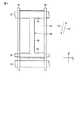
図3は、図2に示した液晶表示パネルLPNの画素PXを対向基板CTの側から見たときのアレイ基板ARの構造を概略的に示す平面図である。 FIG. 3 is a plan view schematically showing the structure of the array substrate AR when the pixel PX of the liquid crystal display panel LPN shown in FIG. 2 is viewed from the counter substrate CT side.
ゲート配線G1、補助容量線C1及びC2は、それぞれ第1方向Xに沿って延在している。ソース配線S1及びS2は、画素電極PEを挟む両側に位置し、それぞれ第2方向Yに沿って延在している。ゲート配線G1は、補助容量線C1と補助容量線C2との間に位置し、補助容量線C2に近接している。 The gate line G1 and the auxiliary capacitance lines C1 and C2 each extend along the first direction X. The source lines S1 and S2 are located on both sides of the pixel electrode PE, and extend along the second direction Y, respectively. The gate line G1 is located between the auxiliary capacitance line C1 and the auxiliary capacitance line C2, and is close to the auxiliary capacitance line C2.
図示した例では、画素PXは、図中の破線で示したように、補助容量線C1及びゲート配線G1とソース配線S1及びS2とが成すマス目の領域に相当し、第1方向Xに沿った長さよりも第2方向Yに沿った長さの方が長い長方形状である。ゲート配線G1は画素PXの一端部に配置され、補助容量線C1は画素PXの他端部に配置されている。ソース配線S1と画素電極PEとの間、及び、ソース配線S2と画素電極PEとの間には、略長方形状の開口部が形成される。 In the illustrated example, the pixel PX corresponds to a square area formed by the storage capacitor line C1, the gate wiring G1, and the source wirings S1 and S2, as indicated by a broken line in the drawing, and extends along the first direction X. The length along the second direction Y is longer than the length. The gate line G1 is disposed at one end of the pixel PX, and the storage capacitor line C1 is disposed at the other end of the pixel PX. A substantially rectangular opening is formed between the source line S1 and the pixel electrode PE and between the source line S2 and the pixel electrode PE.
画素電極PEは、図示を省略したスイッチング素子に電気的に接続されている。この画素電極PEは、第1主電極PA、第1副電極PB、及び、容量部PCを含んでいる。なお、図示した例では、一画素PXに配置された画素電極PEのみが図示されているが、図示を省略した他の画素についても同一形状の画素電極が配置されている。 The pixel electrode PE is electrically connected to a switching element (not shown). The pixel electrode PE includes a first main electrode PA, a first sub electrode PB, and a capacitor portion PC. In the illustrated example, only the pixel electrode PE disposed in one pixel PX is illustrated, but pixel electrodes having the same shape are disposed in other pixels that are not illustrated.
すなわち、第1主電極PAは、第2方向Yに沿って直線的に延在した帯状に形成されている。この第1主電極PAは、ソース配線S1とソース配線S2との間の略中間に位置している。また、この第1主電極PAは、補助容量線C1からゲート配線G1まで延在している。 That is, the first main electrode PA is formed in a strip shape extending linearly along the second direction Y. The first main electrode PA is located approximately in the middle between the source line S1 and the source line S2. The first main electrode PA extends from the auxiliary capacitance line C1 to the gate line G1.
第1副電極PBは、第1方向Xに沿って直線的に延在した帯状に形成されている。この第1副電極PBは、画素PXの一端部に配置され、ソース配線S1とソース配線S2との間のゲート配線G1を覆っている。また、この第1副電極PBは、第1主電極PAの一端部に接続されている。 The first sub-electrode PB is formed in a strip shape extending linearly along the first direction X. The first sub electrode PB is disposed at one end of the pixel PX, and covers the gate line G1 between the source line S1 and the source line S2. The first sub electrode PB is connected to one end of the first main electrode PA.
図示した例では、第1副電極PBの端部は、それぞれソース配線S1のエッジ上及びソース配線S2のエッジ上に位置しているが、それぞれソース配線S1及びソース配線S2の上まで延在していても良い。つまり、第1副電極PBの第1方向Xに沿った長さは、ソース配線S1とソース配線S2との間のゲート配線G1の第1方向Xに沿った長さと同等以上である。また、第1副電極PBの第2方向Yに沿った幅は、ゲート配線G1の第2方向Yに沿った幅と同等以上である。つまり、ソース配線S1とソース配線S2との間において、ゲート配線G1は、第1副電極PBから露出していない。 In the illustrated example, the end portions of the first sub-electrode PB are located on the edge of the source line S1 and the edge of the source line S2, respectively, but extend to above the source line S1 and the source line S2, respectively. May be. That is, the length along the first direction X of the first sub-electrode PB is equal to or greater than the length along the first direction X of the gate line G1 between the source line S1 and the source line S2. In addition, the width along the second direction Y of the first sub-electrode PB is equal to or greater than the width along the second direction Y of the gate wiring G1. That is, the gate line G1 is not exposed from the first sub electrode PB between the source line S1 and the source line S2.
容量部PCは、第1方向Xに沿って直線的に延在した帯状に形成されている。この容量部PCは、画素PXの他端部に配置され、補助容量線C1の直上に配置されている。また、この容量部PCは、第1主電極PAの他端部に電気的に接続されている。なお、この容量部PCは、図示したように、画素電極PEの一部(つまり、第1主電極PAなどと同一材料により一体的に形成されている)であっても良いが、画素電極PEに電気的に接続された他の部材、例えば、スイッチング素子の半導体層やソース配線と同一部材によって形成されても良い。このような容量部PCの第1方向Xに沿った長さは、ソース配線S1とソース配線S2との間の補助容量線C1の第1方向Xに沿った長さと同等以下である。 The capacitor part PC is formed in a belt shape extending linearly along the first direction X. The capacitor portion PC is disposed at the other end portion of the pixel PX, and is disposed immediately above the storage capacitor line C1. In addition, the capacitor portion PC is electrically connected to the other end portion of the first main electrode PA. As shown in the figure, the capacitor portion PC may be a part of the pixel electrode PE (that is, integrally formed of the same material as the first main electrode PA), but the pixel electrode PE. It may be formed of another member electrically connected to the same member, for example, the same member as the semiconductor layer of the switching element and the source wiring. The length of the capacitor portion PC along the first direction X is equal to or less than the length along the first direction X of the storage capacitor line C1 between the source line S1 and the source line S2.
この容量部PCは、補助容量線C1の上方に延在した図示しないスイッチング素子のドレイン電極と電気的に接続されている。これにより、画素電極PEは、スイッチング素子SWと電気的に接続される。また、画素電極PEと補助容量線C1との間に保持容量Csが形成される。 The capacitor portion PC is electrically connected to a drain electrode of a switching element (not shown) extending above the auxiliary capacitance line C1. Thereby, the pixel electrode PE is electrically connected to the switching element SW. In addition, a storage capacitor Cs is formed between the pixel electrode PE and the storage capacitor line C1.
なお、図中のRB1は、アレイ基板ARの表面に配置された第1配向膜の第1ラビング方向を示し、また、図中のRB2は、図示しない対向基板の表面に配置された第2配向膜の第2ラビング方向を示している。これらの第1ラビング方向RB1及び第2ラビング方向RB2は、互いに平行且つ逆向きである。また、これらの第1ラビング方向RB1及び第2ラビング方向RB2は、第2方向Yに対して数°程度わずかに傾いた方向であり、例えば、第1ラビング方向RB1及び第2ラビング方向RB2と第2方向Yとのなす角度は7°である。 In the figure, RB1 indicates the first rubbing direction of the first alignment film disposed on the surface of the array substrate AR, and RB2 in the figure indicates the second alignment disposed on the surface of the counter substrate (not shown). The second rubbing direction of the film is shown. The first rubbing direction RB1 and the second rubbing direction RB2 are parallel and opposite to each other. In addition, the first rubbing direction RB1 and the second rubbing direction RB2 are slightly inclined by several degrees with respect to the second direction Y. For example, the first rubbing direction RB1 and the second rubbing direction RB2 The angle formed by the two directions Y is 7 °.
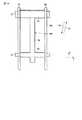
図4は、図2に示した液晶表示パネルLPNの対向基板CTにおける画素PXの構造を概略的に示す平面図である。 FIG. 4 is a plan view schematically showing the structure of the pixel PX on the counter substrate CT of the liquid crystal display panel LPN shown in FIG.
対向電極CEは、第2主電極CA1及びCA2を含んでいる。これらの第2主電極CA1及びCA2は、第2方向Yに沿って直線的に延在した帯状に形成されている。第2主電極CA1は、ソース配線S1の直上に配置されている。第2主電極CA2は、ソース配線S2の直上に配置されている。図示したように、これらのソース配線S1の直上の第2主電極CA1及びソース配線S2の直上の第2主電極CA2と、画素電極PEの第1主電極PAとは、重なることはなく、第1方向Xに沿って一定の間隔を置いて交互に並んでいる。つまり、第1主電極PAと第2主電極CA1及びCA2との第1方向Xに沿った間隔は、略一定である。画素PXのうち、主として表示に寄与する透過部は、第1主電極PAと第2主電極CA1及びCA2との間にそれぞれ形成される。 The counter electrode CE includes second main electrodes CA1 and CA2. These second main electrodes CA1 and CA2 are formed in a strip shape extending linearly along the second direction Y. The second main electrode CA1 is disposed immediately above the source line S1. The second main electrode CA2 is disposed immediately above the source line S2. As illustrated, the second main electrode CA1 directly above the source line S1 and the second main electrode CA2 immediately above the source line S2 and the first main electrode PA of the pixel electrode PE do not overlap each other. They are arranged alternately at a certain interval along one direction X. That is, the distance along the first direction X between the first main electrode PA and the second main electrodes CA1 and CA2 is substantially constant. In the pixel PX, the transmissive portion mainly contributing to display is formed between the first main electrode PA and the second main electrodes CA1 and CA2.
図5は、図2に示した液晶表示パネルLPNの断面構造を概略的に示す図である。なお、図5の(a)はスイッチング素子SWを含む断面図であり、図5の(b)は画素電極PEの第1主電極PAを含む第1方向Xに沿った断面図であり、図5の(c)は画素電極PEの第1副電極PBを含む第1方向Xに沿った断面図である。 FIG. 5 schematically shows a cross-sectional structure of liquid crystal display panel LPN shown in FIG. 5A is a cross-sectional view including the switching element SW, and FIG. 5B is a cross-sectional view along the first direction X including the first main electrode PA of the pixel electrode PE. FIG. 5C is a cross-sectional view along the first direction X including the first sub-electrode PB of the pixel electrode PE.
すなわち、アレイ基板ARは、ガラス基板などの光透過性を有する第1絶縁基板10を用いて形成されている。このアレイ基板ARは、第1絶縁基板10の内面(すなわち、対向基板CTに対向する面)にスイッチング素子SWを備えている。ここに示したスイッチング素子SWは、トップゲート型の薄膜トランジスタである。 That is, the array substrate AR is formed by using a first insulating
スイッチング素子SWは、半導体層SCを備えている。この半導体層SCは、例えば、ポリシリコンやアモルファスシリコンなどによって形成可能であり、ここではポリシリコンによって形成されている。スイッチング素子SWの半導体層SCは、第1絶縁基板10の上に形成されている。半導体層SCは、チャネル領域SCCを挟んだ両側にそれぞれソース領域SCS及びドレイン領域SCDを有している。なお、第1絶縁基板10と半導体層SCとの間には、絶縁膜であるアンダーコート層が介在していても良い。半導体層SCは、ゲート絶縁膜11によって覆われている。また、ゲート絶縁膜11は、第1絶縁基板10の上にも配置されている。 The switching element SW includes a semiconductor layer SC. The semiconductor layer SC can be formed of, for example, polysilicon or amorphous silicon, and is formed of polysilicon here. The semiconductor layer SC of the switching element SW is formed on the first insulating
ゲート電極WGは、ゲート絶縁膜11の上に形成され、半導体層SCのチャネル領域SCCの上方に位置している。ゲート配線G1も、ゲート絶縁膜11の上に形成されている。ゲート電極WGは、ゲート配線G1と電気的に接続されている。なお、このゲート電極WGは、ゲート配線G1の一部であってもよい。 The gate electrode WG is formed on the
これらのゲート電極WG及びゲート配線G1は、図示しない補助容量線C1などとともに同一材料を用いて同一工程で形成可能である。ゲート電極WG及びゲート配線G1は、第1層間絶縁膜12によって覆われている。また、この第1層間絶縁膜12は、ゲート絶縁膜11の上にも配置されている。 The gate electrode WG and the gate wiring G1 can be formed in the same process using the same material together with the auxiliary capacitance line C1 (not shown). The gate electrode WG and the gate wiring G1 are covered with the first
スイッチング素子SWのソース電極WS及びドレイン電極WDは、第1層間絶縁膜12の上に形成されている。ソース電極WSは、ソース配線S1の一部であっても良い。また、この図においては、第1層間絶縁膜12の上に形成されたソース配線S2も図示されている。これらのソース電極WS、ドレイン電極WD、ソース配線S1及びS2は、同一材料を用いて同一工程で形成可能である。 The source electrode WS and the drain electrode WD of the switching element SW are formed on the first
ソース電極WSは、ゲート絶縁膜11及び第1層間絶縁膜12を貫通するコンタクトホールを通して半導体層SCのソース領域SCSにコンタクトしている。ドレイン電極WDは、ゲート絶縁膜11及び第1層間絶縁膜12を貫通するコンタクトホールを通して半導体層SCのドレイン領域SCDにコンタクトしている。これらのゲート電極WG、ソース電極WS、及び、ドレイン電極WDは、例えば、モリブデン、アルミニウム、タングステン、チタンなどの導電材料によって形成されている。 The source electrode WS is in contact with the source region SCS of the semiconductor layer SC through a contact hole that penetrates the
このような構成のスイッチング素子SWは、第2層間絶縁膜13によって覆われている。つまり、ソース電極WS、ドレイン電極WD、ソース配線S1及びS2は、第2層間絶縁膜13によって覆われている。また、この第2層間絶縁膜13は、第1層間絶縁膜12の上にも配置されている。 The switching element SW having such a configuration is covered with the second
画素電極PEは、第2層間絶縁膜13の上に形成さている。この画素電極PEは、第2層間絶縁膜13を貫通するコンタクトホールを介してドレイン電極WDに接続されている。このような画素電極PEは、光透過性を有する導電材料、例えば、インジウム・ティン・オキサイド(ITO)やインジウム・ジンク・オキサイド(IZO)などによって形成されている。 The pixel electrode PE is formed on the second
画素電極PEの第1主電極PAは、第2層間絶縁膜13上において、ソース配線S1の直上の位置p1とソース配線S2の直上の位置p2との略中間に位置している。画素電極PEの第1副電極PBは、第2層間絶縁膜13上において、位置p1から位置p2にわたりゲート配線G1の直上に位置している。 The first main electrode PA of the pixel electrode PE is located on the second
画素電極PEは、第1配向膜14によって覆われている。この第1配向膜14は、第2層間絶縁膜13の上にも配置され、アレイ基板ARの液晶層LQに接する面に設けられている。この第1配向膜14は、水平配向性を示す材料によって形成されており、上述したような第1ラビング方向RB1にラビング処理されている。 The pixel electrode PE is covered with the
一方、対向基板CTは、ガラス基板などの光透過性を有する第2絶縁基板20を用いて形成されている。この対向基板CTは、第2絶縁基板20の内面(すなわち、アレイ基板ARに対向する面)に、カラーフィルタ層21、対向電極CEなどを備えている。 On the other hand, the counter substrate CT is formed using a second insulating
カラーフィルタ層21は、第2絶縁基板20の上に形成されている。このカラーフィルタ層21は、互いに異なる複数の色、例えば赤色、青色、緑色といった3原色にそれぞれ着色された樹脂材料によって形成されている。詳述しないが、赤色に着色された樹脂材料は赤色画素に対応して配置され、同様に、青色に着色された樹脂材料は青色画素に対応して配置され、緑色に着色された樹脂材料は緑色画素に対応して配置されている。 The
対向電極CEは、カラーフィルタ層21の上に形成されている。この対向電極CEは、画素電極PEとの間に横電界を形成するように配置された第2主電極CA1及びCA2を含んでいる。第2主電極CA1及びCA2は、それぞれソース配線S1及びソース配線S2の直上に位置している。このような対向電極CEは、画素電極PEと同様に、ITOやIZOなどの光透過性を有する導電材料によって形成されている。 The counter electrode CE is formed on the
対向電極CEの表面は、第2配向膜22によって覆われている。この第2配向膜22は、カラーフィルタ層21の上にも配置され、対向基板CTの液晶層LQに接する面に設けられている。この第2配向膜22は、第1配向膜14と同様に水平配向性を示す材料によって形成されており、上述したような第2ラビング方向RB2にラビング処理されている。 The surface of the counter electrode CE is covered with the
なお、この対向基板CTにおいて、カラーフィルタ層21と対向電極CE及び第2配向膜22との間には、カラーフィルタ層21の表面の凹凸を平坦化するオーバーコート層が配置されていても良い。 In the counter substrate CT, an overcoat layer for flattening the unevenness of the surface of the
上述したようなアレイ基板ARと対向基板CTとは、それぞれの第1配向膜14及び第2配向膜22が対向するように配置されている。このとき、アレイ基板ARの第1配向膜14と対向基板CTの第2配向膜22との間には、例えば、樹脂材料によって一方の基板に一体的に形成された柱状スペーサが配置され、これにより、所定のギャップ、例えば3〜7μmのセルギャップが形成される。アレイ基板ARと対向基板CTとは、所定のセルギャップが形成された状態で図示しないシール材によって貼り合わせられている。液晶層LQは、上述したセルギャップに封入されている。すなわち、液晶層LQは、アレイ基板ARと対向基板CTとの間に保持されたポジ型の液晶材料によって構成されている。 The array substrate AR and the counter substrate CT as described above are arranged so that the
液晶表示パネルLPNの一方の外面、つまり、アレイ基板ARを構成する第1絶縁基板10の外面には、第1偏光板PL1が接着剤などにより貼付されている。また、液晶表示パネルLPNの他方の外面、つまり、対向基板CTを構成する第2絶縁基板20の外面には、第2偏光板PL2が接着剤などにより貼付されている。 A first polarizing plate PL1 is attached to one outer surface of the liquid crystal display panel LPN, that is, the outer surface of the first insulating
本実施形態においては、第1偏光板PL1の吸収軸と、第2偏光板PL2の吸収軸とが直交する位置関係にあり、ノーマリーブラックモードを実現している。 In this embodiment, the absorption axis of the first polarizing plate PL1 and the absorption axis of the second polarizing plate PL2 are orthogonal to each other, thereby realizing a normally black mode.
すなわち、画素電極PEと対向電極CEとの間に電位差が形成されていない無電界時には、液晶層LQの液晶分子は、第1ラビング方向RB1及び第2ラビング方向RB2に平行な方向に配向している。この状態では、バックライト4からのバックライト光が第2偏光板PL2を透過しないため、画素PXにおいて黒が表示される。 That is, when no electric field is generated between the pixel electrode PE and the counter electrode CE, the liquid crystal molecules of the liquid crystal layer LQ are aligned in a direction parallel to the first rubbing direction RB1 and the second rubbing direction RB2. Yes. In this state, since the backlight from the
一方、画素電極PEと対向電極CEとの間に電位差が形成された状態では、液晶分子は、その長軸が電界の向きと略平行となるように配向する。例えば、第1主電極PAと第2主電極CA1及びCA2との間に横電界が形成された状態では、液晶分子は、この電界に沿って配向する。このため、第1主電極PAと第2主電極CA1及びCA2との間に形成された透過部では、バックライト4からのバックライトが透過し、画素PXにおいて白が表示される。このときの各透過部における液晶分子の主な配向方向は、図4中の矢印D1または矢印D2で示した第1方向Xに略平行な方向である。つまり、各画素PXにおいて、画素電極PEと対向電極CEとの間に電界が形成された状態では、2分割配向されている。 On the other hand, in a state where a potential difference is formed between the pixel electrode PE and the counter electrode CE, the liquid crystal molecules are aligned so that the major axis thereof is substantially parallel to the direction of the electric field. For example, in a state where a horizontal electric field is formed between the first main electrode PA and the second main electrodes CA1 and CA2, the liquid crystal molecules are aligned along this electric field. For this reason, in the transmission part formed between the first main electrode PA and the second main electrodes CA1 and CA2, the backlight from the
なお、このとき、第1主電極PA付近及び第2主電極CA1及びCA2付近では、横電界がほとんど形成されない(あるいは、液晶分子を駆動するのに十分な電界が形成されない)ため、液晶分子は、無電界時と同様に、第1ラビング方向RB1及び第2ラビング方向RB2からほとんど動かない。このため、第1主電極PA及び第2主電極CA1及びCA2は、光透過性の導電材料によって形成されているが、これらの領域ではバックライト光が透過せず、表示に寄与しない(黒)。 At this time, in the vicinity of the first main electrode PA and in the vicinity of the second main electrodes CA1 and CA2, a transverse electric field is hardly formed (or an electric field sufficient to drive the liquid crystal molecules is not formed). As in the case of no electric field, it hardly moves from the first rubbing direction RB1 and the second rubbing direction RB2. For this reason, the first main electrode PA and the second main electrodes CA1 and CA2 are formed of a light-transmitting conductive material. However, backlight light does not pass through these regions and does not contribute to display (black). .
また、第1副電極PBと第2主電極CA1及びCA2との間には電界が形成されるが、第1副電極PBの両端部付近と第2主電極CA1及びCA2との間に縦電界が形成されるため、液晶分子は、立ち上がるように配向する。また、第2副電極PBの中央部付近では、液晶分子を駆動するのに十分な横電界が形成されない。このため、第1副電極PB付近の領域では、バックライト光が透過せず、表示に寄与しない。 An electric field is formed between the first sub-electrode PB and the second main electrodes CA1 and CA2, but a vertical electric field is formed between both ends of the first sub-electrode PB and the second main electrodes CA1 and CA2. Therefore, the liquid crystal molecules are aligned so as to rise. In addition, a lateral electric field sufficient to drive the liquid crystal molecules is not formed near the center of the second sub electrode PB. For this reason, in the region near the first sub electrode PB, the backlight does not transmit and does not contribute to display.
本実施形態の第1構成例によれば、ゲート配線G1の直上には、第1副電極PBが配置されているため、ゲート配線G1からの電界が第2副電極PBによって遮蔽される。このため、ゲート配線G1から液晶層LQに対して不所望なバイアスが印加されることを抑制することができ、焼きツキなどの表示不良の発生を抑制することが可能となる。したがって、表示品位の良好な液晶表示装置を提供することができる。 According to the first configuration example of the present embodiment, since the first sub electrode PB is arranged immediately above the gate line G1, the electric field from the gate line G1 is shielded by the second sub electrode PB. For this reason, it is possible to suppress an undesired bias from being applied to the liquid crystal layer LQ from the gate wiring G1, and it is possible to suppress the occurrence of display defects such as burn-in. Therefore, a liquid crystal display device with good display quality can be provided.
本実施形態において、ライン反転駆動またはドット反転駆動が適用された場合には、対向電極CEの電位に対して図3に示した一画素PXの画素電極PEに印加される電圧の極性と、この画素PXの第2方向Yに隣接する画素の画素電極に印加される電圧の極性とは互いに逆極性となる(つまり、隣接する行間で液晶駆動電圧の極性が反転している)。 In this embodiment, when line inversion driving or dot inversion driving is applied, the polarity of the voltage applied to the pixel electrode PE of one pixel PX shown in FIG. The polarities of the voltages applied to the pixel electrodes of the pixels adjacent to the pixel PX in the second direction Y are opposite to each other (that is, the polarity of the liquid crystal driving voltage is inverted between adjacent rows).
このとき、第2方向Yに隣接する画素間において、一方の液晶駆動電圧が正極性であって、他方の液晶駆動電圧が負極性である場合、これらの画素間に強い横電界が形成される。例えば、対向電極CEの電位を0Vとし、一方の画素の画素電極に印加される電圧が+5Vであり、他方の画素の画素電極に印加される電圧が−5Vである場合、これらの画素電極間の電位差によって強い横電界が形成される。このような横電界の方位は、第2方向Yに沿っており、本来、画素PX内の液晶分子を駆動するのに必要な第1主電極PAと第2主電極CA1及びCA2との間の横電界の方位(第1方向X)とは異なる。このような不所望な横電界の影響により、画素間の境界付近の液晶分子の一部は表示に寄与しない方位に配向し(暗線の発生)、透過率の低下を招く恐れがある。 At this time, if one liquid crystal drive voltage is positive and the other liquid crystal drive voltage is negative between pixels adjacent in the second direction Y, a strong lateral electric field is formed between these pixels. . For example, when the potential of the counter electrode CE is 0 V, the voltage applied to the pixel electrode of one pixel is +5 V, and the voltage applied to the pixel electrode of the other pixel is −5 V, the interval between these pixel electrodes A strong transverse electric field is formed due to the potential difference. The orientation of such a transverse electric field is along the second direction Y, and is essentially between the first main electrode PA and the second main electrodes CA1 and CA2 that are necessary for driving the liquid crystal molecules in the pixel PX. This is different from the direction of the horizontal electric field (first direction X). Due to the influence of such an undesired lateral electric field, some of the liquid crystal molecules in the vicinity of the boundary between the pixels are aligned in an orientation that does not contribute to display (generation of dark lines), which may cause a decrease in transmittance.
本実施形態の第1構成例では、第1副電極PBが画素PXの一端部つまり第2方向Yに隣接する画素間の境界付近に配置されている。この第1副電極PBと第2主電極CA1及びCA2との間に形成される電界は、第2方向Yに隣接する画素間での不所望な電界の発生を抑制する。このため、画素間の境界付近においても、第1副電極PB上では上述した通り表示に寄与しないものの、第1副電極PBの周辺領域では、第2方向Yに隣接する画素間での電界の影響を受けず、表示に寄与するため、暗線の発生を抑制することができる。したがって、画素電極PEが第1副電極PBを有していない場合と比較して、透過率を向上することが可能となる。 In the first configuration example of the present embodiment, the first sub-electrode PB is disposed near one end of the pixel PX, that is, in the vicinity of the boundary between pixels adjacent in the second direction Y. The electric field formed between the first sub electrode PB and the second main electrodes CA1 and CA2 suppresses generation of an undesired electric field between pixels adjacent in the second direction Y. For this reason, even in the vicinity of the boundary between the pixels, the display does not contribute to the display on the first sub-electrode PB as described above, but in the peripheral region of the first sub-electrode PB, the electric field between the pixels adjacent in the second direction Y is reduced. Since it is not affected and contributes to display, the generation of dark lines can be suppressed. Therefore, it is possible to improve the transmittance as compared with the case where the pixel electrode PE does not include the first sub electrode PB.
なお、画素電極PEと対向電極CEとの間に電位差が形成された状態であっても、第1主電極PAや第2主電極CA1及びCA2に重なる領域の液晶分子は、表示に寄与する方位に配向しない場合が多い。このため、画素電極PE及び対向電極CEは、必ずしも透明な導電材料によって形成される必要はなく、アルミニウムや銀などの導電材料を用いて形成しても良い。 Even in the state where a potential difference is formed between the pixel electrode PE and the counter electrode CE, the liquid crystal molecules in the region overlapping the first main electrode PA and the second main electrodes CA1 and CA2 have an orientation that contributes to display. In many cases, it is not oriented. For this reason, the pixel electrode PE and the counter electrode CE are not necessarily formed of a transparent conductive material, and may be formed using a conductive material such as aluminum or silver.
また、第2主電極CA1及びCA2は、それぞれソース配線S1及びソース配線S2の上方(つまりソース配線S1及びS2と向かい合う位置)に配置されている。ソース配線Sは、元々遮光性の導電材料によって形成されているため、第2主電極CA1及びCA2に重なる領域の液晶分子が表示に寄与しない方位に配向したとしても、画素PXの透過率にはほとんど影響を与えない。むしろ、第2主電極CA1及びCA2がソース配線S1及びソース配線S2よりも第1主電極PA側に配置された場合と比較すると、画素PXの透過率は向上する。 The second main electrodes CA1 and CA2 are disposed above the source line S1 and the source line S2 (that is, a position facing the source lines S1 and S2), respectively. Since the source line S is originally formed of a light-shielding conductive material, even if the liquid crystal molecules in the region overlapping the second main electrodes CA1 and CA2 are aligned in an orientation that does not contribute to display, the transmittance of the pixel PX Has little effect. Rather, the transmittance of the pixel PX is improved as compared with the case where the second main electrodes CA1 and CA2 are arranged closer to the first main electrode PA than the source wiring S1 and the source wiring S2.
また、第2主電極CA1及びCA2をソース配線S1及びソース配線S2の上方に配置することによって、第1主電極PAと第2主電極CA1及びCA2との間の距離を拡大することが可能となり、より水平に近い横電界を形成することが可能となる。このため、従来の構成であるIPSモード等の利点である広視野角化も維持される。 Further, by disposing the second main electrodes CA1 and CA2 above the source wiring S1 and the source wiring S2, it is possible to increase the distance between the first main electrode PA and the second main electrodes CA1 and CA2. It is possible to form a lateral electric field that is more horizontal. For this reason, the wide viewing angle, which is an advantage of the IPS mode having the conventional configuration, is also maintained.
なお、アレイ基板ARと対向基板CTとの合わせずれが生じた際に、第1主電極PAを挟んだ両側の第2主電極CA1及びCA2との距離に差が生じることがある。しかしながら、このような合わせずれは、全ての画素PXに共通に生じるため、画素PX間での電界分布に相違はなく、画像の表示に影響を及ぼさない。 When misalignment between the array substrate AR and the counter substrate CT occurs, there may be a difference in the distance between the second main electrodes CA1 and CA2 on both sides of the first main electrode PA. However, since such misalignment occurs in common to all the pixels PX, there is no difference in the electric field distribution between the pixels PX, and the display of the image is not affected.
次に、本実施形態の第2構成例について説明する。この第2構成例は、第1構成例と比較して、画素電極PE及び対向電極CEの形状が異なる点で相違している。なお、この第2構成例において、第1構成例と同一の構成については同一の参照符号を付して詳細な説明を省略する。 Next, a second configuration example of this embodiment will be described. The second configuration example is different from the first configuration example in that the shapes of the pixel electrode PE and the counter electrode CE are different. In the second configuration example, the same components as those in the first configuration example are denoted by the same reference numerals, and detailed description thereof is omitted.
図6は、第2構成例における液晶表示パネルLPNの画素PXを対向基板CTの側から見たときのアレイ基板ARの構造を概略的に示す平面図である。 FIG. 6 is a plan view schematically showing the structure of the array substrate AR when the pixel PX of the liquid crystal display panel LPN in the second configuration example is viewed from the counter substrate CT side.
ゲート配線G1及び補助容量線C1は、それぞれ第1方向Xに沿って延在している。ソース配線S1及びS2は、それぞれ第2方向Yに沿って延在している。図示した例では、ゲート配線G1は画素PXの略中央に配置され、補助容量線C1は画素PXの他端部に配置されている。 The gate line G1 and the auxiliary capacitance line C1 each extend along the first direction X. The source lines S1 and S2 extend along the second direction Y, respectively. In the illustrated example, the gate line G1 is disposed at substantially the center of the pixel PX, and the auxiliary capacitance line C1 is disposed at the other end of the pixel PX.
画素電極PEは、櫛歯電極として、第1主電極PA1及びPA2、第1副電極PB、容量部PC、及び、端部電極PDを含んでいる。なお、図示した例では、第1主電極は2本であるが、1本であっても良いし、3本以上であっても良く、画素電極PEの形状は図示した例に限らない。 The pixel electrode PE includes first main electrodes PA1 and PA2, a first sub electrode PB, a capacitor portion PC, and an end electrode PD as comb-teeth electrodes. In the illustrated example, there are two first main electrodes, but there may be one or three or more, and the shape of the pixel electrode PE is not limited to the illustrated example.
容量部PC、第1主電極PA1、第1副電極PB、第1主電極PA2、及び、端部電極PDは、この順に第2方向Yに沿って略等間隔に並んでおり、また、互いに略平行である。これらの第1主電極PA1及びPA2、第1副電極PB、容量部PC、及び、端部電極PDは、一体的に形成されており、図示した例のように、例えば、ソース配線S2の上で互いに電気的に接続されている。 The capacitor portion PC, the first main electrode PA1, the first sub-electrode PB, the first main electrode PA2, and the end electrode PD are arranged at substantially equal intervals along the second direction Y in this order. It is almost parallel. The first main electrodes PA1 and PA2, the first sub electrode PB, the capacitor portion PC, and the end electrode PD are integrally formed. For example, on the source line S2, as shown in the illustrated example. Are electrically connected to each other.
以下に、各櫛歯電極についてより具体的に説明する。 Below, each comb-tooth electrode is demonstrated more concretely.
すなわち、第1主電極PA1及びPA2は、それぞれ第1方向Xに沿って直線的に延在した帯状に形成されている。これらの第1主電極PA1及びPA2は、ソース配線S1とソース配線S2との間に亘って延在している。第1主電極PA1は、第1副電極PBと容量部PCとの間の略中間に位置している。第2主電極PA2は、第1副電極PBと端部電極PDとの間の略中間に位置している。 That is, the first main electrodes PA1 and PA2 are each formed in a strip shape extending linearly along the first direction X. These first main electrodes PA1 and PA2 extend between the source line S1 and the source line S2. The first main electrode PA1 is located approximately in the middle between the first sub electrode PB and the capacitor part PC. The second main electrode PA2 is located approximately in the middle between the first sub electrode PB and the end electrode PD.
第1副電極PBは、第1方向Xに沿って直線的に延在した帯状に形成されている。この第1副電極PBは、画素PXの略中央部に配置され、第1主電極PA1と第1主電極PA2との間の略中間に位置している。この第1副電極PBは、ソース配線S1とソース配線S2との間のゲート配線G1を覆っている。 The first sub-electrode PB is formed in a strip shape extending linearly along the first direction X. The first sub electrode PB is disposed at a substantially central portion of the pixel PX, and is positioned approximately in the middle between the first main electrode PA1 and the first main electrode PA2. The first sub electrode PB covers the gate line G1 between the source line S1 and the source line S2.
このような第1副電極PBの第1方向Xに沿った長さは、ソース配線S1とソース配線S2との間のゲート配線G1の第1方向Xに沿った長さと同等以上である。また、第1副電極PBの第2方向Yに沿った幅は、ゲート配線G1の第2方向Yに沿った幅と同等以上である。このため、ソース配線S1とソース配線S2との間において、ゲート配線G1は、第1副電極PBから露出していない。 The length along the first direction X of the first sub electrode PB is equal to or longer than the length along the first direction X of the gate line G1 between the source line S1 and the source line S2. In addition, the width along the second direction Y of the first sub-electrode PB is equal to or greater than the width along the second direction Y of the gate wiring G1. Therefore, the gate line G1 is not exposed from the first sub electrode PB between the source line S1 and the source line S2.
容量部PCは、第1方向Xに沿って直線的に延在した帯状に形成されている。この容量部PCは、画素PXの他端部に配置され、補助容量線C1の直上に配置されている。端部電極PDは、第1方向Xに沿って直線的に延在した帯状に形成されている。この端部電極PDは、画素PXの一端部に配置されている。 The capacitor part PC is formed in a belt shape extending linearly along the first direction X. The capacitor portion PC is disposed at the other end portion of the pixel PX, and is disposed immediately above the storage capacitor line C1. The end electrode PD is formed in a strip shape extending linearly along the first direction X. The end electrode PD is disposed at one end of the pixel PX.
なお、第1配向膜の第1ラビング方向RB1及び第2配向膜の第2ラビング方向RB2は、第1構成例と同様に、互いに平行且つ逆向きである。これらの第1ラビング方向RB1及び第2ラビング方向RB2は、第1方向Xに対して数°程度わずかに傾いた方向であり、例えば、第1ラビング方向RB1及び第2ラビング方向RB2と第1方向Xとのなす角度は7°である。 The first rubbing direction RB1 of the first alignment film and the second rubbing direction RB2 of the second alignment film are parallel and opposite to each other, as in the first configuration example. The first rubbing direction RB1 and the second rubbing direction RB2 are slightly inclined by several degrees with respect to the first direction X, for example, the first rubbing direction RB1 and the second rubbing direction RB2 and the first direction. The angle made with X is 7 °.
図7は、第2構成例における液晶表示パネルLPNの対向基板CTにおける画素PXの構造を概略的に示す平面図である。 FIG. 7 is a plan view schematically showing the structure of the pixel PX on the counter substrate CT of the liquid crystal display panel LPN in the second configuration example.
対向電極CEは、複数の第2主電極CA1乃至CA4を含んでいる。なお、図示した例では、第2主電極の本数は4本であるが、画素電極PEの形状に合わせて適宜変更可能である。これらの第2主電極CA1乃至CA4は、第2方向Yに沿って略等間隔に並んでおり、また、互いに略平行である。 The counter electrode CE includes a plurality of second main electrodes CA1 to CA4. In the illustrated example, the number of the second main electrodes is four, but can be appropriately changed according to the shape of the pixel electrode PE. The second main electrodes CA1 to CA4 are arranged at substantially equal intervals along the second direction Y, and are substantially parallel to each other.
このような第2主電極CA1乃至CA4は、第1方向Xに沿って直線的に延在した帯状に形成されている。つまり、第2主電極CA1乃至CA4は、画素電極PEの各櫛歯電極(すなわち、第1主電極PA1及びPA2、第1副電極PB、容量部PC、及び、端部電極PD)と略平行である。また、これらの第2主電極CA1乃至CA4は、画素電極PEの各櫛歯電極と重なることはなく、第2方向Yに沿って各櫛歯電極と略一定の間隔を置いて交互に並んでいる。 The second main electrodes CA1 to CA4 are formed in a strip shape extending linearly along the first direction X. That is, the second main electrodes CA1 to CA4 are substantially parallel to the comb electrodes of the pixel electrode PE (that is, the first main electrodes PA1 and PA2, the first sub electrode PB, the capacitor portion PC, and the end electrode PD). It is. The second main electrodes CA1 to CA4 do not overlap with the comb electrodes of the pixel electrode PE, and are alternately arranged along the second direction Y with the comb electrodes at a substantially constant interval. Yes.
すなわち、第2主電極CA1は、容量部PCと第1主電極PA1との間の略中間の位置している。第2主電極CA2は、第1主電極PA1と第1副電極PBとの間の略中間の位置している。第2主電極CA3は、第1副電極PBと第1主電極PA2との間の略中間の位置している。第2主電極CA4は、第1主電極PA2と端部電極PDとの間の略中間の位置している。 That is, the second main electrode CA1 is positioned approximately in the middle between the capacitor portion PC and the first main electrode PA1. The second main electrode CA2 is positioned approximately in the middle between the first main electrode PA1 and the first sub electrode PB. The second main electrode CA3 is positioned approximately in the middle between the first sub electrode PB and the first main electrode PA2. The second main electrode CA4 is positioned approximately in the middle between the first main electrode PA2 and the end electrode PD.
このような画素PXのうち、主として表示に寄与する透過部は、画素電極PEの各櫛歯電極と第2主電極CA1乃至CA4との間に形成される。画素電極PEと対向電極CEとの間に電界が形成された状態では、各透過部における液晶分子の主な配向方向は、図中の矢印D1または矢印D2で示した第2方向Yに略平行な方向である。つまり、各画素PXにおいて、2分割配向されている。 In such a pixel PX, a transmissive portion mainly contributing to display is formed between each comb electrode of the pixel electrode PE and the second main electrodes CA1 to CA4. In a state where an electric field is formed between the pixel electrode PE and the counter electrode CE, the main alignment direction of the liquid crystal molecules in each transmission part is substantially parallel to the second direction Y indicated by the arrow D1 or the arrow D2 in the drawing. Direction. That is, each pixel PX is divided into two parts.
本実施形態の第2構成例によれば、第1構成例と同様に、ゲート配線G1の直上には、第1副電極PBが配置されているため、ゲート配線G1からの電界が第2副電極PBによって遮蔽される。このため、ゲート配線G1から液晶層LQに対して不所望なバイアスが印加されることを抑制することができ、焼きツキなどの表示不良の発生を抑制することが可能となる。したがって、表示品位の良好な液晶表示装置を提供することができる。 According to the second configuration example of the present embodiment, as in the first configuration example, the first sub-electrode PB is disposed immediately above the gate wiring G1, so that the electric field from the gate wiring G1 is changed to the second sub-electrode. It is shielded by the electrode PB. For this reason, it is possible to suppress an undesired bias from being applied to the liquid crystal layer LQ from the gate wiring G1, and it is possible to suppress the occurrence of display defects such as burn-in. Therefore, a liquid crystal display device with good display quality can be provided.
また、この第2構成例において、ライン反転駆動またはドット反転駆動が適用された場合でも、端部電極PDが画素PXの一端部つまり第2方向Yに隣接する画素間の境界付近に配置されている。この端部電極PDと第2主電極CA4との間に形成される電界は、第2方向Yに隣接する画素間での不所望な電界の発生を抑制する。このため、画素間の境界付近においても、第2方向Yに隣接する画素間での電界の影響を受けず、暗線の発生を抑制することができる。したがって、画素電極PEが端部電極PDを有していない場合と比較して、透過率を向上することが可能となる。 In the second configuration example, even when line inversion driving or dot inversion driving is applied, the end electrode PD is disposed near one end of the pixel PX, that is, in the vicinity of the boundary between pixels adjacent in the second direction Y. Yes. The electric field formed between the end electrode PD and the second main electrode CA4 suppresses generation of an undesired electric field between pixels adjacent in the second direction Y. For this reason, even in the vicinity of the boundary between the pixels, the generation of dark lines can be suppressed without being affected by the electric field between the pixels adjacent in the second direction Y. Therefore, the transmittance can be improved as compared with the case where the pixel electrode PE does not include the end electrode PD.
次に、本実施形態の第3構成例について説明する。この第3構成例は、第1構成例及び第2構成例と比較して、画素電極PE及び対向電極CEの形状が異なる点で相違している。なお、この第3構成例において、第1構成例と同一の構成については同一の参照符号を付して詳細な説明を省略する。 Next, a third configuration example of this embodiment will be described. The third configuration example is different from the first configuration example and the second configuration example in that the shapes of the pixel electrode PE and the counter electrode CE are different. Note that in this third configuration example, the same reference numerals are given to the same configurations as those in the first configuration example, and detailed description thereof is omitted.
図8は、第3構成例における液晶表示パネルLPNの画素PXを対向基板CTの側から見たときのアレイ基板ARの構造を概略的に示す平面図である。 FIG. 8 is a plan view schematically showing the structure of the array substrate AR when the pixel PX of the liquid crystal display panel LPN in the third configuration example is viewed from the counter substrate CT side.
ゲート配線G1及び補助容量線C1は、それぞれ第1方向Xに沿って延在している。ソース配線S1及びS2は、それぞれ第2方向Yに沿って延在している。図示した例では、ゲート配線G1は画素PXの略中央に配置され、補助容量線C1は画素PXの他端部に配置されている。 The gate line G1 and the auxiliary capacitance line C1 each extend along the first direction X. The source lines S1 and S2 extend along the second direction Y, respectively. In the illustrated example, the gate line G1 is disposed at substantially the center of the pixel PX, and the auxiliary capacitance line C1 is disposed at the other end of the pixel PX.
画素電極PEは、第1主電極PA1乃至PA6、第1副電極PB、及び、容量部PCを含んでいる。なお、図示した例では、第1主電極の本数は6本であるが、この例に限らない。これらの第1主電極PA1乃至PA6、第1副電極PB、及び、容量部PCは、一体的に形成されており、図示した例のように、例えば、ソース配線S1の上で互いに電気的に接続されている。 The pixel electrode PE includes first main electrodes PA1 to PA6, a first sub electrode PB, and a capacitor portion PC. In the illustrated example, the number of first main electrodes is six, but is not limited to this example. The first main electrodes PA1 to PA6, the first sub-electrode PB, and the capacitor portion PC are integrally formed, and are electrically connected to each other on the source line S1, for example, as shown in the illustrated example. It is connected.
第1主電極PA1乃至PA6は、それぞれ第1方向X及び第2方向Yに対して交差する斜め方向に沿って直線的に延在した帯状に形成されている。第1主電極PA1乃至PA3は、第1副電極PBと容量部PCとの間における画素PXの上側半分に配置され、略等間隔に並んでおり、互いに略平行である。第1主電極PA4乃至PA5は、画素PXの下側半分に配置され、略等間隔に並んでおり、互いに略平行である。 The first main electrodes PA1 to PA6 are each formed in a strip shape extending linearly along an oblique direction intersecting the first direction X and the second direction Y. The first main electrodes PA1 to PA3 are arranged in the upper half of the pixel PX between the first sub electrode PB and the capacitor part PC, are arranged at substantially equal intervals, and are substantially parallel to each other. The first main electrodes PA4 to PA5 are arranged in the lower half of the pixel PX, are arranged at substantially equal intervals, and are substantially parallel to each other.
これらの第1主電極PA1乃至PA3が延在する方向と、第1主電極PA4乃至PA5が延在する方向とは平行ではない。また、第1主電極PA1乃至PA3のそれぞれは、画素PXの略中央に配置された第1副電極PBを挟んで、第1主電極PA4乃至PA5のそれぞれと略線対称である。 The direction in which the first main electrodes PA1 to PA3 extend is not parallel to the direction in which the first main electrodes PA4 to PA5 extend. In addition, each of the first main electrodes PA1 to PA3 is substantially line symmetric with each of the first main electrodes PA4 to PA5 with the first sub electrode PB disposed substantially at the center of the pixel PX interposed therebetween.
第1副電極PBは、第1方向Xに沿って直線的に延在した帯状に形成されている。この第1副電極PBは、画素PXの略中央部に配置され、ソース配線S1とソース配線S2との間のゲート配線G1を覆っている。このような第1副電極PBの第1方向Xに沿った長さは、ソース配線S1とソース配線S2との間のゲート配線G1の第1方向Xに沿った長さと同等以上である。また、第1副電極PBの第2方向Yに沿った幅は、ゲート配線G1の第2方向Yに沿った幅と同等以上である。このため、ソース配線S1とソース配線S2との間において、ゲート配線G1は、第1副電極PBから露出していない。 The first sub-electrode PB is formed in a strip shape extending linearly along the first direction X. The first sub-electrode PB is disposed substantially at the center of the pixel PX, and covers the gate line G1 between the source line S1 and the source line S2. The length along the first direction X of the first sub electrode PB is equal to or longer than the length along the first direction X of the gate line G1 between the source line S1 and the source line S2. In addition, the width along the second direction Y of the first sub-electrode PB is equal to or greater than the width along the second direction Y of the gate wiring G1. Therefore, the gate line G1 is not exposed from the first sub electrode PB between the source line S1 and the source line S2.
容量部PCは、第1方向Xに沿って直線的に延在した帯状に形成されている。この容量部PCは、画素PXの他端部に配置され、補助容量線C1の直上に配置されている。 The capacitor part PC is formed in a belt shape extending linearly along the first direction X. The capacitor portion PC is disposed at the other end portion of the pixel PX, and is disposed immediately above the storage capacitor line C1.
なお、第1配向膜の第1ラビング方向RB1及び第2配向膜の第2ラビング方向RB2は、第1構成例と同様に、互いに平行且つ逆向きである。これらの第1ラビング方向RB1及び第2ラビング方向RB2は、第1方向と略平行な方向である。 The first rubbing direction RB1 of the first alignment film and the second rubbing direction RB2 of the second alignment film are parallel and opposite to each other, as in the first configuration example. The first rubbing direction RB1 and the second rubbing direction RB2 are directions substantially parallel to the first direction.
図9は、第3構成例における液晶表示パネルLPNの対向基板CTにおける画素PXの構造を概略的に示す平面図である。 FIG. 9 is a plan view schematically showing the structure of the pixel PX on the counter substrate CT of the liquid crystal display panel LPN in the third configuration example.
対向電極CEは、複数の第2主電極CA1乃至CA4、及び、第1副電極CBを含んでいる。なお、図示した例では、第2主電極の本数は4本であるが、画素電極PEの形状に合わせて適宜変更可能である。これらの第2主電極CA1乃至CA4、及び、第2副電極CBは、一体的に形成されており、互いに電気的に接続されている。 The counter electrode CE includes a plurality of second main electrodes CA1 to CA4 and a first sub electrode CB. In the illustrated example, the number of the second main electrodes is four, but can be appropriately changed according to the shape of the pixel electrode PE. The second main electrodes CA1 to CA4 and the second sub electrode CB are integrally formed and are electrically connected to each other.
これらの第2主電極CA1乃至CA4は、それぞれ第1方向X及び第2方向Yに対して交差する斜め方向に沿って直線的に延在した帯状に形成されている。第2主電極CA1及びCA2が延在する方向と、第2主電極CA3及びCA4が延在する方向とは平行ではない。また、第2主電極CA1及びCA2のそれぞれは、画素PXの略中央に配置された第2副電極CBを挟んで、第2主電極CA3及びCA4のそれぞれと略線対称である。 These second main electrodes CA1 to CA4 are each formed in a strip shape extending linearly along an oblique direction intersecting the first direction X and the second direction Y. The direction in which the second main electrodes CA1 and CA2 extend is not parallel to the direction in which the second main electrodes CA3 and CA4 extend. In addition, each of the second main electrodes CA1 and CA2 is substantially line symmetric with each of the second main electrodes CA3 and CA4 with the second sub-electrode CB disposed substantially at the center of the pixel PX interposed therebetween.
第2主電極CA1及びCA2は、画素PXの上側半分に配置され、略等間隔に並んでおり、互いに略平行である。また、これらの第2主電極CA1及びCA2は、第1主電極PA1乃至PA3と略平行である。また、これらの第2主電極CA1及びCA2は、第1主電極PA1乃至PA3と重なることはなく、略一定の間隔を置いて交互に並んでいる。すなわち、第2主電極CA1は、第1主電極PA1と第1主電極PA2との間の略中間の位置している。第2主電極CA2は、第1主電極PA2と第1主電極PA3との間の略中間の位置している。 The second main electrodes CA1 and CA2 are arranged in the upper half of the pixel PX, are arranged at substantially equal intervals, and are substantially parallel to each other. The second main electrodes CA1 and CA2 are substantially parallel to the first main electrodes PA1 to PA3. Further, the second main electrodes CA1 and CA2 do not overlap with the first main electrodes PA1 to PA3, and are alternately arranged at a substantially constant interval. That is, the second main electrode CA1 is positioned approximately in the middle between the first main electrode PA1 and the first main electrode PA2. The second main electrode CA2 is positioned approximately in the middle between the first main electrode PA2 and the first main electrode PA3.
第2主電極CA3及びCA4は、画素PXの下側半分に配置され、略等間隔に並んでおり、互いに略平行である。また、これらの第2主電極CA3及びCAは、第1主電極PA4乃至PA6と略平行である。また、これらの第2主電極CA3及びCA4は、第1主電極PA4乃至PA6と重なることはなく、略一定の間隔を置いて交互に並んでいる。すなわち、第2主電極CA3は、第1主電極PA4と第1主電極PA5との間の略中間の位置している。第2主電極CA4は、第1主電極PA5と第1主電極PA6との間の略中間の位置している。 The second main electrodes CA3 and CA4 are arranged in the lower half of the pixel PX, are arranged at substantially equal intervals, and are substantially parallel to each other. The second main electrodes CA3 and CA are substantially parallel to the first main electrodes PA4 to PA6. Further, the second main electrodes CA3 and CA4 do not overlap with the first main electrodes PA4 to PA6, but are alternately arranged at a substantially constant interval. That is, the second main electrode CA3 is positioned approximately in the middle between the first main electrode PA4 and the first main electrode PA5. The second main electrode CA4 is located approximately in the middle between the first main electrode PA5 and the first main electrode PA6.
第2副電極CBは、第1方向Xに沿って直線的に延在した帯状に形成されている。この第2副電極CBは、画素PXの略中央部に配置され、第1副電極PBの直上に延在している。 The second sub electrode CB is formed in a belt shape extending linearly along the first direction X. The second sub electrode CB is disposed at a substantially central portion of the pixel PX and extends immediately above the first sub electrode PB.
このような画素PXのうち、主として表示に寄与する透過部は、画素電極PEの第1主電極PA1乃至PA6と第2主電極CA1乃至CA4との間に形成される。画素電極PEと対向電極CEとの間に電界が形成された状態では、各透過部における液晶分子の主な配向方向は、図中の矢印D1乃至D4のいずれかで示した方向である。つまり、各画素PXにおいて、4分割配向されている。 In such a pixel PX, a transmissive portion mainly contributing to display is formed between the first main electrodes PA1 to PA6 and the second main electrodes CA1 to CA4 of the pixel electrode PE. In a state where an electric field is formed between the pixel electrode PE and the counter electrode CE, the main alignment direction of the liquid crystal molecules in each transmission portion is a direction indicated by any of arrows D1 to D4 in the drawing. That is, each pixel PX is divided into four parts.
本実施形態の第3構成例によれば、第1構成例と同様に、ゲート配線G1の直上には、第1副電極PBが配置されているため、ゲート配線G1からの電界が第2副電極PBによって遮蔽される。このため、ゲート配線G1から液晶層LQに対して不所望なバイアスが印加されることを抑制することができ、焼きツキなどの表示不良の発生を抑制することが可能となる。したがって、表示品位の良好な液晶表示装置を提供することができる。 According to the third configuration example of the present embodiment, as in the first configuration example, since the first sub-electrode PB is disposed immediately above the gate line G1, the electric field from the gate line G1 is changed to the second sub-field. It is shielded by the electrode PB. For this reason, it is possible to suppress an undesired bias from being applied to the liquid crystal layer LQ from the gate wiring G1, and it is possible to suppress the occurrence of display defects such as burn-in. Therefore, a liquid crystal display device with good display quality can be provided.
また、この第3構成例によれば、1画素PXにおいては、液晶分子の配向方向が異なる4つの領域が形成され、しかも、各領域の占める割合が略同等である。このため、それぞれの領域が光学的に補償し合い、広い視野角範囲に亘って均一な表示を実現することが可能となる。 Further, according to the third configuration example, in one pixel PX, four regions having different alignment directions of liquid crystal molecules are formed, and the proportions occupied by the regions are substantially equal. For this reason, each region optically compensates for each other, and a uniform display can be realized over a wide viewing angle range.
また、この第3構成例によれば、画素電極PEの第1副電極PBと、対向電極CEの第2副電極CBとが平行に且つ液晶層LQを介して重なるように配置されているため、画素電極PEと対向電極CEとの間に電位差が形成された際には、これらの間に縦電界が形成される。このような縦電界は、画素PXの上側半分と下側半分とを仕切り、液晶分子を基板に対して略垂直に配向させる。 Further, according to the third configuration example, the first sub-electrode PB of the pixel electrode PE and the second sub-electrode CB of the counter electrode CE are arranged so as to overlap in parallel via the liquid crystal layer LQ. When a potential difference is formed between the pixel electrode PE and the counter electrode CE, a vertical electric field is formed between them. Such a vertical electric field partitions the upper half and the lower half of the pixel PX and aligns the liquid crystal molecules substantially perpendicular to the substrate.
このような縦電界の作用により、画素PXの上側半分において矢印D1または矢印D2の方向に液晶分子を配向させた状態を保持できるとともに、画素PXの下側半分において矢印D3または矢印D4の方向に液晶分子を配向させた状態を保持することが可能となる。このため、1画素PXにおいて、液晶分子の配向が異なる4つの領域のそれぞれの占める割合も略同等に維持することが可能となる。これにより、液晶表示パネルLPNに対して押圧するような応力が加わったとしても、1画素PX内において液晶分子の配向乱れの発生が抑制でき、瞬時に元の配向状態に復帰することが可能となる。 By such an action of the vertical electric field, the liquid crystal molecules can be kept aligned in the direction of the arrow D1 or the arrow D2 in the upper half of the pixel PX, and in the direction of the arrow D3 or the arrow D4 in the lower half of the pixel PX. It becomes possible to maintain the state in which the liquid crystal molecules are aligned. For this reason, in one pixel PX, it is possible to maintain substantially the same proportion of each of the four regions having different liquid crystal molecule orientations. As a result, even if a stress that presses against the liquid crystal display panel LPN is applied, the occurrence of alignment disorder of the liquid crystal molecules in one pixel PX can be suppressed, and the original alignment state can be instantaneously restored. Become.
以下に、実施例1及び2と、比較例1及び2についてそれぞれ説明する。 Examples 1 and 2 and Comparative Examples 1 and 2 will be described below.
≪実施例1≫
この実施例1に係る画素PXの構造は、上記の第1構成例に相当する。Example 1
The structure of the pixel PX according to the first embodiment corresponds to the first configuration example described above.
すなわち、アレイ基板ARに形成された画素電極PEは、隣接する2本のソース配線S1とソース配線S2との間の中央部に形成した第1主電極PA1と、第1主電極PAの一端部に形成した第1副電極PBと、第1主電極PAの他端部に形成した容量部PCと、を有している。第1主電極PAの第1方向Xに沿った幅を10μmとした。 That is, the pixel electrode PE formed on the array substrate AR includes a first main electrode PA1 formed at the center between two adjacent source lines S1 and S2, and one end of the first main electrode PA. The first sub-electrode PB is formed on the first main electrode PA, and the capacitor PC is formed on the other end of the first main electrode PA. The width along the first direction X of the first main electrode PA was 10 μm.
対向基板CTに形成された対向電極CEは、第1主電極PAと平行かつソース配線S1及びソース配線S2の直上に形成した第2主電極CAを有している。第2主電極CAの第1方向Xに沿った幅を10μmとした。 The counter electrode CE formed on the counter substrate CT has a second main electrode CA formed in parallel with the first main electrode PA and immediately above the source line S1 and the source line S2. The width along the first direction X of the second main electrode CA was 10 μm.
アレイ基板ARの表面には第1配向膜14を形成した。また、対向基板CTの表面には第1配向膜22を形成した。これらの第1配向膜14及び第2配向膜22は、水平配向性を有する材料を70nmの厚さで塗布した後に、ラビング処理することによって形成した。第1配向膜14の第1ラビング方向RB1及び第2配向膜22の第2ラビング方向RB2は、第1方向Xを0°方位とし、第2方向Yを90°方位としたとき、83°方位に設定した。 A
アレイ基板ARと対向基板CTとの間のセルギャップを4.0μmとし、アレイ基板ARと対向基板CTとを貼り合わせた。このとき、第1主電極PAと第2主電極CAとの間隔は10μmに設定した。これらのアレイ基板ARと対向基板CTとの間には、メルク社製ポジ型液晶材料を注入して画素ピッチ40μmの液晶表示パネルLPNを作製した。 The cell gap between the array substrate AR and the counter substrate CT was 4.0 μm, and the array substrate AR and the counter substrate CT were bonded together. At this time, the interval between the first main electrode PA and the second main electrode CA was set to 10 μm. A liquid crystal display panel LPN having a pixel pitch of 40 μm was manufactured by injecting a Merck positive liquid crystal material between the array substrate AR and the counter substrate CT.
≪比較例1≫
この比較例1は、実施例1の構成から画素電極PEの第1副電極PBを省略した構成に相当する。それ以外については、上記した実施例1と同様にして液晶表示パネルLPNを作製した。≪Comparative example 1≫
The comparative example 1 corresponds to a configuration in which the first sub electrode PB of the pixel electrode PE is omitted from the configuration of the first embodiment. Otherwise, a liquid crystal display panel LPN was produced in the same manner as in Example 1 described above.
上記した実施例1及び比較例1のそれぞれの液晶表示パネルLPNについて、画素電極PEと対向電極CEとの間に同一の電位差を与えたときの透過率を測定した。比較例1の液晶表示パネルLPNで得られた透過率を1としたとき、実施例1の液晶表示パネルLPNで得られた透過率は1.3であった。このような比較実験により、実施例1の構成によれば、高透過率化を実現できることが確認された。 For each of the liquid crystal display panels LPN of Example 1 and Comparative Example 1 described above, the transmittance was measured when the same potential difference was applied between the pixel electrode PE and the counter electrode CE. When the transmittance obtained with the liquid crystal display panel LPN of Comparative Example 1 was 1, the transmittance obtained with the liquid crystal display panel LPN of Example 1 was 1.3. From such a comparative experiment, it was confirmed that according to the configuration of Example 1, high transmittance can be realized.
≪実施例2≫
この実施例2に係る画素PXの構造は、上記の第3構成例に相当する。<< Example 2 >>
The structure of the pixel PX according to the second embodiment corresponds to the third configuration example described above.
すなわち、アレイ基板ARに形成された画素電極PEは、斜め方向に沿って形成した6本の第1主電極PA1乃至PA6と、第1方向Xに沿って形成した第1副電極PB及び容量部PCと、を有している。 That is, the pixel electrode PE formed on the array substrate AR includes six first main electrodes PA1 to PA6 formed along the oblique direction, the first sub electrode PB formed along the first direction X, and the capacitor portion. PC.
対向基板CTに形成された対向電極CEは、第1主電極PAと平行な方向に沿って形成した4本の第2主電極CA1乃至CA4と、第1方向Xに沿って形成した第2副電極CBと、を有している。 The counter electrode CE formed on the counter substrate CT includes four second main electrodes CA1 to CA4 formed along a direction parallel to the first main electrode PA, and a second sub electrode formed along the first direction X. And an electrode CB.
アレイ基板ARの表面には第1配向膜14を形成した。また、対向基板CTの表面には第1配向膜22を形成した。これらの第1配向膜14及び第2配向膜22は、水平配向性を有する材料を70nmの厚さで塗布した後に、ラビング処理することによって形成した。第1配向膜14の第1ラビング方向RB1及び第2配向膜22の第2ラビング方向RB2は、第1方向Xを0°方位とし、第2方向Yを90°方位としたとき、0°方位に設定した。 A
アレイ基板ARと対向基板CTとの間のセルギャップを4.0μmとし、アレイ基板ARと対向基板CTとを貼り合わせた。このとき、第1主電極PAと第2主電極CAとの間隔は10μmに設定した。これらのアレイ基板ARと対向基板CTとの間には、メルク社製ポジ型液晶材料を注入して画素ピッチ40μmの液晶表示パネルLPNを作製した。 The cell gap between the array substrate AR and the counter substrate CT was 4.0 μm, and the array substrate AR and the counter substrate CT were bonded together. At this time, the interval between the first main electrode PA and the second main electrode CA was set to 10 μm. A liquid crystal display panel LPN having a pixel pitch of 40 μm was manufactured by injecting a Merck positive liquid crystal material between the array substrate AR and the counter substrate CT.
≪比較例2≫
この比較例2は、実施例2の構成から対向電極CEの第2副電極CBを省略した構成に相当する。それ以外については、上記した実施例2と同様にして液晶表示パネルLPNを作製した。«Comparative example 2»
The comparative example 2 corresponds to a configuration in which the second sub electrode CB of the counter electrode CE is omitted from the configuration of the second embodiment. Otherwise, a liquid crystal display panel LPN was produced in the same manner as in Example 2 described above.
上記した実施例2及び比較例2のそれぞれの液晶表示パネルLPNについて、画素電極PEと対向電極CEとの間に同一の電位差を与えたときの液晶分子の配向強度を測定した。ここで、配向強度とは、液晶表示パネルLPNに一定の応力を加えた後、所定時間が経過してから液晶表示パネルLPNを観察したときに応力の痕跡が視認される視角で定義する。 For each of the liquid crystal display panels LPN of Example 2 and Comparative Example 2 described above, the alignment strength of the liquid crystal molecules when the same potential difference was applied between the pixel electrode PE and the counter electrode CE was measured. Here, the orientation strength is defined as a viewing angle at which a trace of stress is visually recognized when a predetermined time elapses after a certain stress is applied to the liquid crystal display panel LPN and the liquid crystal display panel LPN is observed.
つまり、液晶表示パネルLPNに応力を加えると、画素PXにおいて液晶分子の配向乱れが発生し、時間の経過に伴って元の配向状態に復元する場合もあるし、配向乱れが発生した状態で保持されてしまう場合もある。画素PXにおいて比較的小規模な配向乱れが残っている場合、あるいは、元の配向状態に復元した場合には、液晶表示パネルLPNを観察したとき、液晶表示パネルLPNの法線方向から次第に視角を拡大しても、応力の痕跡が視認されることはない。しかしながら、画素PX内で比較的大規模な配向乱れが残っている場合には、液晶表示パネルLPNを観察したとき、液晶表示パネルLPNの法線方向からわずかに視角を拡大しただけで、配向乱れが応力の痕跡として視認されてしまう。このように、応力の痕跡が視認される視角が大きいほど、配向強度が高い(つまり、元の配向状態に復元する復元力あるいは配向安定性が高い)こと示し、逆に、応力の痕跡が視認される視角が小さいほど、配向強度が低いことを示す。 In other words, when stress is applied to the liquid crystal display panel LPN, alignment disorder of the liquid crystal molecules occurs in the pixel PX, and the original alignment state may be restored with time, or the alignment disorder is maintained. It may be done. When a relatively small alignment disorder remains in the pixel PX or when the original alignment state is restored, when the liquid crystal display panel LPN is observed, the viewing angle gradually increases from the normal direction of the liquid crystal display panel LPN. Even if it expands, the trace of stress is not visually recognized. However, in the case where a relatively large alignment disorder remains in the pixel PX, when the liquid crystal display panel LPN is observed, the alignment disorder is merely increased from the normal direction of the liquid crystal display panel LPN. Will be visually recognized as a trace of stress. Thus, the greater the viewing angle at which the trace of stress is visually recognized, the higher the orientation strength (that is, the higher the restoring force or orientation stability to restore the original orientation state), and conversely, the trace of stress is visible. The smaller the viewing angle, the lower the orientation strength.
この実験では、比較例2では法線に対して約20°の視角で応力の痕跡が視認されたのに対して、実施例2では法線から視角を約90°まで拡大しても応力の痕跡は視認されず、配向強度が高いことが確認された。 In this experiment, in Comparative Example 2, a trace of stress was visually recognized at a viewing angle of about 20 ° with respect to the normal line, whereas in Example 2, the stress was observed even when the viewing angle was expanded from the normal line to about 90 °. The trace was not visually recognized, and it was confirmed that the orientation strength was high.
以上説明したように、本実施形態によれば、透過率及び配向強度を向上することが可能であり、表示品位の良好な液晶表示装置を提供することができる。 As described above, according to the present embodiment, it is possible to improve the transmittance and the alignment strength, and it is possible to provide a liquid crystal display device with a good display quality.
なお、この発明は、上記実施形態そのものに限定されるものではなく、その実施の段階ではその要旨を逸脱しない範囲で構成要素を変形して具体化できる。また、上記実施形態に開示されている複数の構成要素の適宜な組み合せにより種々の発明を形成できる。例えば、実施形態に示される全構成要素から幾つかの構成要素を削除してもよい。更に、異なる実施形態に亘る構成要素を適宜組み合せてもよい。 In addition, this invention is not limited to the said embodiment itself, In the stage of implementation, it can change and implement a component within the range which does not deviate from the summary. Further, various inventions can be formed by appropriately combining a plurality of constituent elements disclosed in the embodiment. For example, some components may be deleted from all the components shown in the embodiment. Furthermore, you may combine suitably the component covering different embodiment.
例えば、第1構成例において、第1副電極PB及びゲート配線G1は、画素PXの一端部に配置された例について説明したが、ライン反転駆動またはドット反転駆動以外の駆動方法が適用される場合については、これらの第1副電極PB及びゲート配線G1が必ずしも画素PXの一端部に配置されていなくても良い。例えば、図10に示した例のように、第1副電極PB及びゲート配線G1は、画素PXの一端部よりも中央部寄りに配置されても良い。この場合、第1副電極PBは、第1主電極PAと十字に交差する。このような構成であっても、第1副電極PBは、ゲート配線G1を覆うように配置されているため、第1構成例と同様の効果が得られる。
以下に本件出願当初の特許請求の範囲に記載された発明を付記する。
[C1]
第1方向に沿って延在したゲート配線と、第1方向に直交する第2方向に沿ってそれぞれ延在した第1ソース配線及び第2ソース配線と、前記第1ソース配線と前記第2ソース配線との略中間に位置し第2方向に沿って延在した帯状の第1主電極及び前記第1ソース配線と前記第2ソース配線との間の前記ゲート配線を覆い第1方向に沿って延在した帯状の第1副電極を含む画素電極と、を備えた第1基板と、
前記第1ソース配線及び前記第2ソース配線の直上に配置され第2方向に沿って延在した帯状の第2主電極を含む対向電極と、を備えた第2基板と、
前記第1基板と前記第2基板との間に保持された液晶層と、
を備えたことを特徴とする液晶表示装置。
[C2]
前記ゲート配線及び前記第1副電極は画素の一端部に配置され、
ライン反転駆動またはドット反転駆動が適用されたことを特徴とするC1に記載の液晶表示装置。
[C3]
第1方向に沿って延在したゲート配線と、第1方向に直交する第2方向に沿ってそれぞれ延在した第1ソース配線及び第2ソース配線と、第1方向に沿って延在した帯状の第1主電極及び前記第1ソース配線と前記第2ソース配線との間の前記ゲート配線を覆い第1方向に沿って延在した帯状の第1副電極を含む画素電極と、を備えた第1基板と、
前記第1主電極と前記第1副電極との略中間に位置し第1方向に沿って延在した帯状の第2主電極を含む対向電極と、を備えた第2基板と、
前記第1基板と前記第2基板との間に保持された液晶層と、
を備えたことを特徴とする液晶表示装置。
[C4]
さらに、前記第1基板は、画素の一端部に配置され前記画素電極と電気的に接続されるとともに第1方向に沿って延在した帯状の端部電極を備え、
ライン反転駆動またはドット反転駆動が適用されたことを特徴とするC3に記載の液晶表示装置。
[C5]
前記ゲート配線及び前記第1副電極は、画素の略中央に配置されたことを特徴とするC3またはC4に記載の液晶表示装置。
[C6]
第1方向に沿って延在したゲート配線と、第1方向に直交する第2方向に沿ってそれぞれ延在した第1ソース配線及び第2ソース配線と、第1方向及び第2方向に対して交差する斜め方向に沿って延在した帯状の第1主電極及び前記第1ソース配線と前記第2ソース配線との間の前記ゲート配線を覆い第1方向に沿って延在した帯状の第1副電極を含む画素電極と、を備えた第1基板と、
前記第1主電極と平行な斜め方向に沿って延在した帯状の第2主電極及び前記第1副電極の直上に配置され第1方向に沿って延在した第2副電極を含む対向電極と、を備えた第2基板と、
前記第1基板と前記第2基板との間に保持された液晶層と、
を備えたことを特徴とする液晶表示装置。
[C7]
前記ゲート配線、前記第1副電極、及び、前記第2副電極は、画素の略中央に配置されたことを特徴とするC6に記載の液晶表示装置。
[C8]
さらに、前記第1基板は、画素の他端部に配置され第1方向に沿って延在した補助容量線と、前記第1補助容量線の直上に配置され且つ前記画素電極と電気的に接続された容量部と、を備えたことを特徴とするC1乃至C7のいずれか1項に記載の液晶表示装置。
[C9]
前記第1主電極と前記第2主電極との間に表示に寄与する透過部を形成することを特徴とするC1乃至C8のいずれか1項に記載の液晶表示装置。
[C10]
さらに、前記第1基板は前記画素電極を覆うとともに第1ラビング方向にラビング処理された第1配向膜を備え、前記第2基板は前記対向電極を覆うとともに第1ラビング方向と平行且つ逆向きの第2ラビング方向にラビング処理された第2配向膜を備え、
前記第1ラビング方向及び前記第2ラビング方向は、前記第1主電極及び前記第2主電極と斜めに交差する方向であることを特徴とするC1乃至C9のいずれか1項に記載の液晶表示装置。For example, in the first configuration example, the example in which the first sub-electrode PB and the gate wiring G1 are arranged at one end of the pixel PX has been described. However, a driving method other than line inversion driving or dot inversion driving is applied. As for the first sub-electrode PB and the gate wiring G1, the first sub-electrode PB and the gate wiring G1 are not necessarily arranged at one end of the pixel PX. For example, as in the example illustrated in FIG. 10, the first sub electrode PB and the gate line G1 may be disposed closer to the center than one end of the pixel PX. In this case, the first sub electrode PB intersects the first main electrode PA in a cross shape. Even in such a configuration, since the first sub-electrode PB is disposed so as to cover the gate wiring G1, the same effect as in the first configuration example can be obtained.
The invention described in the scope of the claims at the beginning of the present application is added below.
[C1]
A gate line extending along the first direction; a first source line and a second source line extending along a second direction orthogonal to the first direction; the first source line and the second source; A belt-shaped first main electrode that is positioned approximately in the middle of the wiring and extends in the second direction and the gate wiring between the first source wiring and the second source wiring are covered along the first direction. A first substrate including a pixel electrode including an extended strip-shaped first sub-electrode;
A second substrate comprising: a counter electrode including a strip-shaped second main electrode disposed immediately above the first source wiring and the second source wiring and extending along a second direction;
A liquid crystal layer held between the first substrate and the second substrate;
A liquid crystal display device comprising:
[C2]
The gate wiring and the first sub electrode are disposed at one end of a pixel,
The liquid crystal display device according to C1, wherein line inversion driving or dot inversion driving is applied.
[C3]
A gate line extending along the first direction, a first source line and a second source line extending along a second direction orthogonal to the first direction, and a strip shape extending along the first direction And a pixel electrode including a strip-shaped first sub-electrode extending along a first direction so as to cover the first main electrode and the gate wiring between the first source wiring and the second source wiring. A first substrate;
A second substrate comprising: a counter electrode including a strip-shaped second main electrode positioned substantially in the middle of the first main electrode and the first sub electrode and extending along a first direction;
A liquid crystal layer held between the first substrate and the second substrate;
A liquid crystal display device comprising:
[C4]
Furthermore, the first substrate includes a band-shaped end electrode that is disposed at one end of a pixel, is electrically connected to the pixel electrode, and extends along the first direction.
The liquid crystal display device according to C3, wherein line inversion driving or dot inversion driving is applied.
[C5]
The liquid crystal display device according to C3 or C4, wherein the gate line and the first sub-electrode are arranged at substantially the center of the pixel.
[C6]
A gate wiring extending along the first direction, a first source wiring and a second source wiring extending along a second direction orthogonal to the first direction, and the first direction and the second direction, respectively. A strip-shaped first main electrode extending along an intersecting diagonal direction and a strip-shaped first main electrode covering the gate wiring between the first source wiring and the second source wiring and extending along the first direction. A first substrate including a pixel electrode including a sub-electrode;
A counter electrode including a strip-shaped second main electrode extending along an oblique direction parallel to the first main electrode and a second sub electrode disposed immediately above the first sub electrode and extending along the first direction A second substrate comprising:
A liquid crystal layer held between the first substrate and the second substrate;
A liquid crystal display device comprising:
[C7]
The liquid crystal display device according to C6, wherein the gate wiring, the first sub-electrode, and the second sub-electrode are arranged in a substantially center of a pixel.
[C8]
Further, the first substrate is disposed at the other end of the pixel and extends along the first direction, and is disposed immediately above the first auxiliary capacitor line and is electrically connected to the pixel electrode. The liquid crystal display device according to any one of C1 to C7, further comprising: a capacitor portion.
[C9]
The liquid crystal display device according to any one of C1 to C8, wherein a transmissive portion contributing to display is formed between the first main electrode and the second main electrode.
[C10]
Further, the first substrate includes a first alignment film that covers the pixel electrode and is rubbed in a first rubbing direction, and the second substrate covers the counter electrode and is parallel to and opposite to the first rubbing direction. A second alignment film that is rubbed in the second rubbing direction;
The liquid crystal display according to any one of C1 to C9, wherein the first rubbing direction and the second rubbing direction are directions that obliquely intersect the first main electrode and the second main electrode. apparatus.
LPN…液晶表示パネル
AR…アレイ基板 CT…対向基板 LQ…液晶層
PE…画素電極
PA…第1主電極 PB…第1副電極 PC…容量部 PD…端部電極
CE…対向電極
CA…第2主電極 CB…第2副電極
S…ソース配線
G…ゲート配線
C…補助容量線LPN ... Liquid crystal display panel AR ... Array substrate CT ... Counter substrate LQ ... Liquid crystal layer PE ... Pixel electrode
PA ... first main electrode PB ... first sub electrode PC ... capacitor part PD ... end electrode CE ... counter electrode CA ... second main electrode CB ... second sub electrode S ... source wiring G ... gate wiring C ... auxiliary capacitance line
Claims (7)
Translated fromJapanese前記第1ソース配線及び前記第2ソース配線の直上に配置され第2方向に沿って延在した帯状の第2主電極を含む対向電極と、を備えた第2基板と、
前記第1基板と前記第2基板との間に保持された液晶層と、
を備え、
第2方向に隣接する画素の画素電極に印加される電圧が逆極性となるライン反転駆動またはドット反転駆動が適用されたことを特徴とする液晶表示装置。A gate linedisposed at one end of the pixel and extending along a first direction; a first source line and a second source line extending along a second direction orthogonal to the first direction; Between the first source line and the second source lineat one end of the band-shaped first main electrode and thepixel, which is located approximately in the middle between the source line and the second source line and extends in the second direction. And a pixel electrode including a strip-shaped first sub-electrode that covers the gate wiring and extends along the first direction,
A second substrate comprising: a counter electrode including a strip-shaped second main electrode disposed immediately above the first source wiring and the second source wiring and extending along a second direction;
A liquid crystal layer held between the first substrate and the second substrate;
Equipped witha,
A liquid crystal display device, whereinline inversion driving or dot inversion driving in which a voltage applied to a pixel electrode of a pixel adjacent in the second direction has a reverse polarity is applied .
前記第1主電極と前記第1副電極との略中間に位置し第1方向に沿って延在した帯状の第2主電極を含む対向電極と、を備えた第2基板と、
前記第1基板と前記第2基板との間に保持された液晶層と、
を備え、
第2方向に隣接する画素の画素電極に印加される電圧が逆極性となるライン反転駆動またはドット反転駆動が適用されたことを特徴とする液晶表示装置。A gate line extending along the first direction, a first source line and a second source line extending along a second direction orthogonal to the first direction, and a strip shape extending along the first direction A pixel electrode including a first sub-electrode extending in the first direction so as to cover the first main electrode and the gate line between the first source line and the second source line, andone end of thepixel A first substrate havinga strip-shaped end electrode disposed in a portion and electrically connected to the pixel electrode and extending in a first direction ;
A second substrate comprising: a counter electrode including a strip-shaped second main electrode positioned substantially in the middle of the first main electrode and the first sub electrode and extending along a first direction;
A liquid crystal layer held between the first substrate and the second substrate;
Equipped witha,
A liquid crystal display device, whereinline inversion driving or dot inversion driving in which a voltage applied to a pixel electrode of a pixel adjacent in the second direction has a reverse polarity is applied .
前記第1主電極と平行な斜め方向に沿って延在した帯状の第2主電極及び前記第1副電極の直上に配置され第1方向に沿って延在した第2副電極を含む対向電極と、を備えた第2基板と、
前記第1基板と前記第2基板との間に保持された液晶層と、
を備え、
前記ゲート配線、前記第1副電極、及び、前記第2副電極は、画素の略中央に配置されたことを特徴とする液晶表示装置。A gate wiring extending along the first direction, a first source wiring and a second source wiring extending along a second direction orthogonal to the first direction, and the first direction and the second direction, respectively. A strip-shaped first main electrode extending along an intersecting diagonal direction and a strip-shaped first main electrode covering the gate wiring between the first source wiring and the second source wiring and extending along the first direction. A first substrate including a pixel electrode including a sub-electrode;
A counter electrode including a strip-shaped second main electrode extending along an oblique direction parallel to the first main electrode and a second sub electrode disposed immediately above the first sub electrode and extending along the first direction A second substrate comprising:
A liquid crystal layer held between the first substrate and the second substrate;
Equipped witha,
The liquid crystal display device, wherein the gate wiring, the first sub-electrode, and the second sub-electrode are arranged at a substantially center of a pixel .
前記第1ラビング方向及び前記第2ラビング方向は、前記第1主電極及び前記第2主電極と斜めに交差する方向であることを特徴とする請求項1乃至6のいずれか1項に記載の液晶表示装置。Further, the first substrate includes a first alignment film that covers the pixel electrode and is rubbed in a first rubbing direction, and the second substrate covers the counter electrode and is parallel to and opposite to the first rubbing direction. A second alignment film that is rubbed in the second rubbing direction;
The said 1st rubbing direction and the said 2nd rubbing direction are the directions which cross | intersect the said 1st main electrode and the said 2nd main electrode diagonally, The any one of Claim 1 thru | or6 characterized by the above-mentioned. Liquid crystal display device.
Priority Applications (5)
| Application Number | Priority Date | Filing Date | Title |
|---|---|---|---|
| JP2010235368AJP5380416B2 (en) | 2010-10-20 | 2010-10-20 | Liquid crystal display |
| US13/242,321US9395586B2 (en) | 2010-10-20 | 2011-09-23 | Liquid crystal display device |
| TW100135342ATWI459102B (en) | 2010-10-20 | 2011-09-29 | Liquid crystal display device |
| CN201110311039.1ACN102455557B (en) | 2010-10-20 | 2011-10-14 | Liquid crystal indicator |
| US15/181,609US20160357074A1 (en) | 2010-10-20 | 2016-06-14 | Liquid crystal display device |
Applications Claiming Priority (1)
| Application Number | Priority Date | Filing Date | Title |
|---|---|---|---|
| JP2010235368AJP5380416B2 (en) | 2010-10-20 | 2010-10-20 | Liquid crystal display |
Publications (2)
| Publication Number | Publication Date |
|---|---|
| JP2012088542A JP2012088542A (en) | 2012-05-10 |
| JP5380416B2true JP5380416B2 (en) | 2014-01-08 |
Family
ID=45972761
Family Applications (1)
| Application Number | Title | Priority Date | Filing Date |
|---|---|---|---|
| JP2010235368AActiveJP5380416B2 (en) | 2010-10-20 | 2010-10-20 | Liquid crystal display |
Country Status (4)
| Country | Link |
|---|---|
| US (2) | US9395586B2 (en) |
| JP (1) | JP5380416B2 (en) |
| CN (1) | CN102455557B (en) |
| TW (1) | TWI459102B (en) |
Families Citing this family (13)
| Publication number | Priority date | Publication date | Assignee | Title |
|---|---|---|---|---|
| JP5380416B2 (en)* | 2010-10-20 | 2014-01-08 | 株式会社ジャパンディスプレイ | Liquid crystal display |
| JP5695946B2 (en) | 2011-03-17 | 2015-04-08 | 株式会社ジャパンディスプレイ | Liquid crystal display |
| WO2012137540A1 (en)* | 2011-04-08 | 2012-10-11 | 株式会社ジャパンディスプレイセントラル | Liquid crystal display device |
| JP5504215B2 (en) | 2011-07-08 | 2014-05-28 | 株式会社ジャパンディスプレイ | Liquid crystal display |
| JP5386555B2 (en) | 2011-07-28 | 2014-01-15 | 株式会社ジャパンディスプレイ | Liquid crystal display |
| JP5520896B2 (en) | 2011-08-08 | 2014-06-11 | 株式会社ジャパンディスプレイ | Liquid crystal display |
| JP5577308B2 (en) | 2011-08-25 | 2014-08-20 | 株式会社ジャパンディスプレイ | Liquid crystal display |
| JP5845035B2 (en) | 2011-09-28 | 2016-01-20 | 株式会社ジャパンディスプレイ | Liquid crystal display |
| JP5953120B2 (en)* | 2012-05-25 | 2016-07-20 | 株式会社ジャパンディスプレイ | Liquid crystal display |
| JP5906138B2 (en)* | 2012-05-29 | 2016-04-20 | 株式会社ジャパンディスプレイ | Liquid crystal display |
| JP5827970B2 (en)* | 2013-03-25 | 2015-12-02 | 株式会社ジャパンディスプレイ | Display device and electronic device |
| JP6336762B2 (en) | 2014-01-24 | 2018-06-06 | 株式会社ジャパンディスプレイ | Liquid crystal display |
| KR102498553B1 (en)* | 2015-11-19 | 2023-02-10 | 티씨엘 차이나 스타 옵토일렉트로닉스 테크놀로지 컴퍼니 리미티드 | Apparatus for manufacturing diplay device and method for manufacturing display device |
Family Cites Families (33)
| Publication number | Priority date | Publication date | Assignee | Title |
|---|---|---|---|---|
| JPH06222397A (en) | 1993-01-25 | 1994-08-12 | Sony Corp | Liquid crystal display device |
| JPH07159807A (en) | 1993-12-06 | 1995-06-23 | Hitachi Ltd | Active matrix liquid crystal display device |
| TW454101B (en) | 1995-10-04 | 2001-09-11 | Hitachi Ltd | In-plane field type liquid crystal display device comprising liquid crystal molecules with more than two different kinds of reorientation directions and its manufacturing method |
| TW505801B (en)* | 1995-10-12 | 2002-10-11 | Hitachi Ltd | In-plane field type liquid crystal display device comprising a structure prevented from charging with electricity |
| US5745207A (en)* | 1995-11-30 | 1998-04-28 | Matsushita Electric Industrial Co., Ltd. | Active matrix liquid crystal display having electric fields parallel to substrates |
| JPH09160041A (en) | 1995-12-08 | 1997-06-20 | Toshiba Corp | Liquid crystal display device |
| JPH09160061A (en) | 1995-12-08 | 1997-06-20 | Toshiba Corp | Liquid crystal display device |
| JPH09160042A (en) | 1995-12-08 | 1997-06-20 | Toshiba Corp | Liquid crystal display device |
| JP3486859B2 (en)* | 1996-06-14 | 2004-01-13 | 大林精工株式会社 | Liquid crystal display |
| JPH1026765A (en) | 1996-07-10 | 1998-01-27 | Toshiba Corp | Liquid crystal display element, projection type liquid crystal display device and substrate |
| JP3644653B2 (en) | 1996-08-07 | 2005-05-11 | 三菱電機株式会社 | Liquid crystal display |
| JPH1090708A (en) | 1996-09-17 | 1998-04-10 | Toshiba Corp | Liquid crystal display device |
| JP3966614B2 (en)* | 1997-05-29 | 2007-08-29 | 三星電子株式会社 | Wide viewing angle LCD |
| JP3107000B2 (en)* | 1997-06-30 | 2000-11-06 | 日本電気株式会社 | Liquid crystal display |
| JP4364332B2 (en)* | 1998-06-23 | 2009-11-18 | シャープ株式会社 | Liquid crystal display |
| KR100767364B1 (en)* | 2001-06-19 | 2007-10-17 | 삼성전자주식회사 | LCD and its driving method |
| JP4373052B2 (en)* | 2002-05-06 | 2009-11-25 | 大林精工株式会社 | Ultra high aperture ratio wide viewing angle LCD |
| JP4262501B2 (en)* | 2002-07-08 | 2009-05-13 | シャープ株式会社 | Liquid crystal display |
| US20040109119A1 (en) | 2002-12-05 | 2004-06-10 | Hannstar Display Corporation | In-plane switching liquid crystal display with high aperture ratio |
| JP4107978B2 (en) | 2003-02-21 | 2008-06-25 | スタンレー電気株式会社 | Liquid crystal display element |
| US8390548B2 (en)* | 2003-05-15 | 2013-03-05 | Sharp Kabushiki Kaisha | Liquid crystal display device and driving method thereof |
| JP2005003802A (en) | 2003-06-10 | 2005-01-06 | Toshiba Matsushita Display Technology Co Ltd | Liquid crystal display device |
| JP4088619B2 (en) | 2004-01-28 | 2008-05-21 | シャープ株式会社 | Active matrix substrate and display device |
| KR100617040B1 (en) | 2004-03-16 | 2006-08-30 | 엘지.필립스 엘시디 주식회사 | Transverse electric field liquid crystal display device and manufacturing method thereof |
| JP2005292515A (en) | 2004-03-31 | 2005-10-20 | Sharp Corp | Liquid crystal display device, driving method thereof, and electronic apparatus |
| KR101247113B1 (en) | 2005-11-22 | 2013-04-01 | 삼성디스플레이 주식회사 | Display apparatus |
| TW200813535A (en) | 2006-09-12 | 2008-03-16 | Wintek Corp | Liquid crystal panel and liquid crystal display |
| KR101413275B1 (en) | 2007-01-29 | 2014-06-30 | 삼성디스플레이 주식회사 | Liquid crystal display panel and manufacturing method thereof |
| KR20080071231A (en) | 2007-01-30 | 2008-08-04 | 삼성전자주식회사 | Liquid crystal display |
| KR101427708B1 (en)* | 2007-02-01 | 2014-08-11 | 삼성디스플레이 주식회사 | Liquid crystal display panel |
| JP4678031B2 (en)* | 2008-01-11 | 2011-04-27 | ソニー株式会社 | Liquid crystal device and electronic device |
| JP4693131B2 (en)* | 2008-02-14 | 2011-06-01 | 東芝モバイルディスプレイ株式会社 | Liquid crystal display |
| JP5380416B2 (en)* | 2010-10-20 | 2014-01-08 | 株式会社ジャパンディスプレイ | Liquid crystal display |
- 2010
- 2010-10-20JPJP2010235368Apatent/JP5380416B2/enactiveActive
- 2011
- 2011-09-23USUS13/242,321patent/US9395586B2/enactiveActive
- 2011-09-29TWTW100135342Apatent/TWI459102B/enactive
- 2011-10-14CNCN201110311039.1Apatent/CN102455557B/enactiveActive
- 2016
- 2016-06-14USUS15/181,609patent/US20160357074A1/ennot_activeAbandoned
Also Published As
| Publication number | Publication date |
|---|---|
| CN102455557A (en) | 2012-05-16 |
| JP2012088542A (en) | 2012-05-10 |
| TW201219940A (en) | 2012-05-16 |
| US20160357074A1 (en) | 2016-12-08 |
| TWI459102B (en) | 2014-11-01 |
| US9395586B2 (en) | 2016-07-19 |
| US20120099070A1 (en) | 2012-04-26 |
| CN102455557B (en) | 2016-05-18 |
Similar Documents
| Publication | Publication Date | Title |
|---|---|---|
| JP5380416B2 (en) | Liquid crystal display | |
| JP5035931B2 (en) | Liquid crystal display | |
| JP5552457B2 (en) | Liquid crystal display | |
| JP5941756B2 (en) | Liquid crystal display | |
| JP5759813B2 (en) | Liquid crystal display | |
| JP5597557B2 (en) | Liquid crystal display | |
| JP2015079207A (en) | Display device | |
| JP5530971B2 (en) | Liquid crystal display | |
| JP5883721B2 (en) | Liquid crystal display | |
| JP2013250411A (en) | Liquid crystal display device | |
| JP5572562B2 (en) | Liquid crystal display | |
| JP6039914B2 (en) | Liquid crystal display | |
| JP5903309B2 (en) | Liquid crystal display | |
| JP5572603B2 (en) | Liquid crystal display | |
| JP2012226283A (en) | Liquid crystal display device | |
| JP5674587B2 (en) | Liquid crystal display | |
| JP6010330B2 (en) | Liquid crystal display | |
| JP2014115561A (en) | Liquide crystal display device | |
| JP2013064800A (en) | Liquid crystal display device | |
| JP2013029784A (en) | Liquid crystal display device | |
| JP2013072954A (en) | Liquid crystal display device | |
| JP5663436B2 (en) | Liquid crystal display | |
| JP6476269B2 (en) | Display device | |
| JP2013068848A (en) | Liquid crystal display device | |
| JP2013101214A (en) | Liquid crystal display device |
Legal Events
| Date | Code | Title | Description |
|---|---|---|---|
| A977 | Report on retrieval | Free format text:JAPANESE INTERMEDIATE CODE: A971007 Effective date:20120905 | |
| A131 | Notification of reasons for refusal | Free format text:JAPANESE INTERMEDIATE CODE: A131 Effective date:20121002 | |
| A521 | Request for written amendment filed | Free format text:JAPANESE INTERMEDIATE CODE: A523 Effective date:20121130 | |
| A711 | Notification of change in applicant | Free format text:JAPANESE INTERMEDIATE CODE: A712 Effective date:20130711 | |
| TRDD | Decision of grant or rejection written | ||
| A01 | Written decision to grant a patent or to grant a registration (utility model) | Free format text:JAPANESE INTERMEDIATE CODE: A01 Effective date:20130903 | |
| A61 | First payment of annual fees (during grant procedure) | Free format text:JAPANESE INTERMEDIATE CODE: A61 Effective date:20130930 | |
| R150 | Certificate of patent or registration of utility model | Free format text:JAPANESE INTERMEDIATE CODE: R150 Ref document number:5380416 Country of ref document:JP Free format text:JAPANESE INTERMEDIATE CODE: R150 | |
| R250 | Receipt of annual fees | Free format text:JAPANESE INTERMEDIATE CODE: R250 | |
| R250 | Receipt of annual fees | Free format text:JAPANESE INTERMEDIATE CODE: R250 | |
| R250 | Receipt of annual fees | Free format text:JAPANESE INTERMEDIATE CODE: R250 | |
| R250 | Receipt of annual fees | Free format text:JAPANESE INTERMEDIATE CODE: R250 | |
| R250 | Receipt of annual fees | Free format text:JAPANESE INTERMEDIATE CODE: R250 | |
| R250 | Receipt of annual fees | Free format text:JAPANESE INTERMEDIATE CODE: R250 | |
| R250 | Receipt of annual fees | Free format text:JAPANESE INTERMEDIATE CODE: R250 | |
| R250 | Receipt of annual fees | Free format text:JAPANESE INTERMEDIATE CODE: R250 | |
| R250 | Receipt of annual fees | Free format text:JAPANESE INTERMEDIATE CODE: R250 | |
| S111 | Request for change of ownership or part of ownership | Free format text:JAPANESE INTERMEDIATE CODE: R313113 | |
| R350 | Written notification of registration of transfer | Free format text:JAPANESE INTERMEDIATE CODE: R350 |