JP5376850B2 - Solar cell enabling photoelectric conversion in a wide wavelength range - Google Patents
Solar cell enabling photoelectric conversion in a wide wavelength rangeDownload PDFInfo
- Publication number
- JP5376850B2 JP5376850B2JP2008184929AJP2008184929AJP5376850B2JP 5376850 B2JP5376850 B2JP 5376850B2JP 2008184929 AJP2008184929 AJP 2008184929AJP 2008184929 AJP2008184929 AJP 2008184929AJP 5376850 B2JP5376850 B2JP 5376850B2
- Authority
- JP
- Japan
- Prior art keywords
- solar cell
- dye
- transport layer
- cell according
- photoelectric conversion
- Prior art date
- Legal status (The legal status is an assumption and is not a legal conclusion. Google has not performed a legal analysis and makes no representation as to the accuracy of the status listed.)
- Expired - Fee Related
Links
Images


Classifications
- Y—GENERAL TAGGING OF NEW TECHNOLOGICAL DEVELOPMENTS; GENERAL TAGGING OF CROSS-SECTIONAL TECHNOLOGIES SPANNING OVER SEVERAL SECTIONS OF THE IPC; TECHNICAL SUBJECTS COVERED BY FORMER USPC CROSS-REFERENCE ART COLLECTIONS [XRACs] AND DIGESTS
- Y02—TECHNOLOGIES OR APPLICATIONS FOR MITIGATION OR ADAPTATION AGAINST CLIMATE CHANGE
- Y02E—REDUCTION OF GREENHOUSE GAS [GHG] EMISSIONS, RELATED TO ENERGY GENERATION, TRANSMISSION OR DISTRIBUTION
- Y02E10/00—Energy generation through renewable energy sources
- Y02E10/50—Photovoltaic [PV] energy
- Y02E10/542—Dye sensitized solar cells
Landscapes
- Photovoltaic Devices (AREA)
- Hybrid Cells (AREA)
- Connection Of Batteries Or Terminals (AREA)
Description
Translated fromJapanese本発明は、太陽電池に関する。 The present invention relates to a solar cell.
太陽電池の太陽光に対する効率を向上させる一般的な方法は、光吸収帯域を増大することである。その一つが、タンデム型に太陽電池を積層する方法である。 A common way to improve the efficiency of solar cells against sunlight is to increase the light absorption band. One of them is a method of stacking solar cells in a tandem type.
従来のタンデム型セルは、図1に示すように、セルを前後に積層させたものであり、高コストな材料である透明導電膜等を多く使用しなければならないために、コスト高になる等の問題点があった。例えば、非特許文献1は、CIGS(Copper Indium Gallium DiSelenide)化合物半導体を用いた太陽電池と色素増感太陽電池をスタックしたものであり、非特許文献2は、チタニア塗布透明導電膜ガラス基板/白金メッシュ電極/チタニア塗布透明導電膜ガラス基板からなるセルであり、非特許文献3は、チタニア塗布透明導電膜ガラス基板/白金メッシュ電極/酸化ニッケル塗布透明導電膜ガラス基板からなるセルであり、非特許文献4は、異なる色素を有する色素増感太陽電池をスタックしたものであるが、いずれの技術においてもコスト高になる等の問題点があった。また、これらの従来技術は、単に光電変換素子を重ねた場合、各材料が光を吸収するために、積層した奥の光電変換素子に有効に光が届かなくなるという欠点があった。さらに、部材を省略し、光電変換素子の光吸収層、電荷分離層を積層した場合には、第1の光電変換素子と第2の光電変換素子を接合する技術が難しく、大きな電流の損失を招く等の欠点があった。 As shown in FIG. 1, the conventional tandem type cell is obtained by laminating the cells in the front and rear, and it is necessary to use a large amount of transparent conductive film, which is a high-cost material. There was a problem. For example, Non-Patent Document 1 is a stack of a solar cell using CIGS (Copper Indium Gallium DiSelenide) compound semiconductor and a dye-sensitized solar cell, and Non-Patent
また、シリコン系太陽電池を用いた平面型のタンデム型太陽電池は、従来から知られていたが、自由にエネルギーレベルや色を変えることができず、平面型タンデム型太陽電池の利点を活かすことができなかった。
本発明の課題は、効率の良い太陽電池を提供することにある。 An object of the present invention is to provide an efficient solar cell.
本発明は、下記に示すとおりの太陽電池を提供するものである。
項1. 太陽光を分光する分光手段を有し、該分光手段により分光した光を受光して光電変換する2個以上の光電変換素子が平面状に配列され、それぞれの光電変換素子が、直列および/または並列で電気的に結合されている太陽電池であって、それぞれの光電変換素子が、分光された光を吸収する受光体、電荷分離界面および電荷輸送層を有し、該受光体、該電荷分離界面および該電荷輸送層の少なくとも一つが有機物であることを特徴とする太陽電池。
項2. 受光体が無機色素または有機色素であることを特徴とする項1に記載の太陽電池。
項3. 電荷分離界面が無機色素または有機色素に接していることを特徴とする項1に記載の太陽電池。
項4. 電荷輸送層が無機電荷移動媒体または有機電荷移動媒体であることを特徴とする項1に記載の太陽電池。The present invention provides a solar cell as described below.
Item 1. Two or more photoelectric conversion elements that have a spectral means for spectrally separating sunlight, receive light split by the spectral means, and perform photoelectric conversion are arranged in a plane, and each photoelectric conversion element is connected in series and / or A solar cell that is electrically coupled in parallel, each photoelectric conversion element having a light-receiving body that absorbs the dispersed light, a charge separation interface, and a charge transport layer, the light-receiving body, the charge separation At least one of the interface and the charge transport layer is an organic material.
Item 3.
Item 4.
以下、本発明を詳細に説明する。 Hereinafter, the present invention will be described in detail.
本発明の太陽電池は、平面的に展開できるため、材料を重ねることによる光吸収のロスがなくなり、かつ、光電変換素子を接合させる必要がないため、接合に起因する電流ロスもない。比較的容易にタンデム構造が形成でき、しかも広帯域の光を吸収し、バンド構造のミスマッチによる効率の低下を防ぎ、高効率を達成できる。そして、この平面タンデム型太陽電池の主体を有機物とすることにより、エネルギーレベルや色を変える選択肢が拡がり、平面型タンデムを無限に並べることが可能となる。 Since the solar cell of the present invention can be developed in a plane, there is no loss of light absorption due to overlapping materials, and there is no current loss due to the junction because there is no need to join the photoelectric conversion element. A tandem structure can be formed relatively easily, and broadband light can be absorbed, a decrease in efficiency due to mismatch of band structures can be prevented, and high efficiency can be achieved. By making the main body of the planar tandem solar cell an organic substance, options for changing the energy level and color are expanded, and it becomes possible to arrange the planar tandem infinitely.
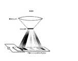
本発明の太陽電池(平面タンデムセル)の一例を図2に示す。太陽光を分光する手段を有し、該分光手段により分光した光をそれぞれの分光範囲(波長領域)で最大の効率が得られる特性を有する光電変換素子を分光面に沿って平面状に展開した太陽電池である。分光の光範囲に応じて最適な光電変換素子を配列することにより、バンド構造のミスマッチによる効率低下が防止でき、さらに広帯域の光を吸収することができる。 An example of the solar cell (planar tandem cell) of the present invention is shown in FIG. A photoelectric conversion element having a characteristic for obtaining the maximum efficiency in each spectral range (wavelength region) of the light dispersed by the spectral means is developed in a plane along the spectral plane. It is a solar cell. By arranging the optimum photoelectric conversion elements according to the light range of the spectrum, it is possible to prevent a decrease in efficiency due to the mismatch of the band structure and to absorb light in a wider band.
本発明の太陽電池における受光体は、幅広い分光特性に吸収を最適化させる必要があり、シャープな光吸収を有する有機色素が有効である。色素増感太陽電池、ハイブリッド色素増感太陽電池として知られている有機系太陽電池は、有機色素または無機色素を受光体として使用できるため、本発明の平面タンデムセルの最適な太陽電池候補である。 The photoreceptor in the solar cell of the present invention must be optimized for absorption over a wide range of spectral characteristics, and organic dyes having sharp light absorption are effective. Organic solar cells known as dye-sensitized solar cells and hybrid dye-sensitized solar cells are suitable solar cell candidates for the planar tandem cell of the present invention because organic dyes or inorganic dyes can be used as photoreceptors. .
本発明に係る電荷輸送層は、電子やホールを輸送する層であり、無機電荷移動媒体または有機電荷移動媒体であるのが好ましい。電子を輸送する材料としては、例えば、n型半導体である酸化亜鉛、酸化錫等の酸化物半導体、フラーレン、フッ素化フタロシアニン等の有機n型半導体が挙げられる。また、ホールを輸送する材料としては、例えば、p型半導体である酸化ニッケル、ヨウ化銅、ポリチオフェン、ポリピロール、PPV等が挙げられる。これらの材料は、分子構造の最適化により、エネルギー順位や色を自由にコントロールでき、平面インフィニットタンデムに最適である。 The charge transport layer according to the present invention is a layer that transports electrons and holes, and is preferably an inorganic charge transfer medium or an organic charge transfer medium. Examples of materials that transport electrons include oxide semiconductors such as zinc oxide and tin oxide, which are n-type semiconductors, and organic n-type semiconductors such as fullerene and fluorinated phthalocyanine. Examples of materials that transport holes include nickel oxide, copper iodide, polythiophene, polypyrrole, and PPV, which are p-type semiconductors. These materials can be freely controlled in energy order and color by optimizing the molecular structure, and are optimal for planar infinite tandem.
本願明細書において、受光体とは色素を意味する。図3に示すように、この色素に光照射がなされると、励起され、電子とホールができる。この色素励起に伴う電子は、エネルギー差があるために、電荷分離界面を通じて、金属酸化物(n型半導体である酸化亜鉛、酸化錫等の酸化物半導体)やフラーレン、フッ素化フタロシアニン等の有機n型半導体に移行する。酸化物半導体や有機n型半導体は、電子輸送層として働く。また、電解質(例えば、ヨウ素30mM、LiI 500mM、ターシャリブチルピリジン500mM、メチルイミダゾリウムアイオダイド500mMのアセトニトリル溶液等)や、p型半導体である酸化ニッケル、ヨウ化銅、高分子(例えば、ポリチオフェン、ポリピロール、PPV)等は、ホール輸送層として働く。電荷輸送層は、これらの電子輸送層とホール輸送層を含む。 In this specification, the photoreceptor means a dye. As shown in FIG. 3, when this dye is irradiated with light, it is excited to generate electrons and holes. Since the electrons due to the excitation of the dye have an energy difference, organic n such as metal oxides (oxide semiconductors such as zinc oxide and tin oxide, which are n-type semiconductors), fullerenes, and fluorinated phthalocyanines are passed through the charge separation interface. Transition to type semiconductor. An oxide semiconductor or an organic n-type semiconductor functions as an electron transport layer. Moreover, electrolytes (for example, iodine 30 mM, LiI 500 mM, tertiary butylpyridine 500 mM, methylimidazolium iodide 500 mM in acetonitrile), p-type semiconductors such as nickel oxide, copper iodide, polymers (for example, polythiophene, Polypyrrole, PPV) and the like serve as a hole transport layer. The charge transport layer includes these electron transport layer and hole transport layer.
本発明の太陽電池は、平面的に展開できるため、材料を重ねることによる光吸収のロスがなくなり、かつ、光電変換素子を接合させる必要がないため、接合に起因する電流ロスもない。比較的容易にタンデム構造が形成でき、しかも広帯域の光を吸収し、バンド構造のミスマッチによる効率の低下を防ぎ、高効率を達成できる。そして、この平面タンデム型太陽電池の主体を有機物とすることにより、エネルギーレベルや色を変える選択肢が拡がり、平面型タンデムを無限に並べることが可能となる。 Since the solar cell of the present invention can be developed in a plane, there is no loss of light absorption due to overlapping materials, and there is no current loss due to the junction because there is no need to join the photoelectric conversion element. A tandem structure can be formed relatively easily, and broadband light can be absorbed, a decrease in efficiency due to mismatch of band structures can be prevented, and high efficiency can be achieved. By making the main body of the planar tandem solar cell an organic substance, options for changing the energy level and color are expanded, and it becomes possible to arrange the planar tandem infinitely.
以下、実施例を挙げて本発明を説明するが、本発明はこれらの実施例に限定されるものではない。 EXAMPLES Hereinafter, although an Example is given and this invention is demonstrated, this invention is not limited to these Examples.
実施例1
図2に示すように、太陽光を石英レンズで集光し、その後、プリズムで分光し、基板上に分光した光を照射できるようにセルを配置した。Example 1
As shown in FIG. 2, the cells were arranged so that sunlight was collected by a quartz lens, then dispersed by a prism, and irradiated on the substrate.
具体的には、セルAとして、透明導電膜(SnO2/F)を表面に形成したガラス基板(表面抵抗10Ω.□)上にソラロニクス社製チタニアペーストDを塗布した後、450℃で30分間加熱することにより、膜厚12μmのポーラスチタニア膜を有する基板を作製した(セルサイズ5×20 mm)。この基板を短波長吸収に適した下記式の色素1-1(エタノール溶液0.1%)に5時間、室温で浸漬した後、エタノールで十分洗浄し、室温下、暗所で乾燥した。対極には、チタン板に白金をスパッタ(100nm)したものを用いた。2枚の基板を、スペーサーとしてハイミラン(DuPont社製、厚さ25μm)を用いて接着した。2枚の基板の隙間に、電解液を注入した。電解液としては、ヨウ素30mM、LiI 500mM、ターシャリブチルピリジン500mM、メチルイミダゾリウムアイオダイド500mMのアセトニトリル溶液を用いた。このようにして、短波長側に感度を有するセルAを作製した。Specifically, after applying a titania paste D made by Solaronics on a glass substrate (surface resistance 10Ω. □) on the surface of which a transparent conductive film (SnO2 / F) is formed as a cell A, at 450 ° C. for 30 minutes By heating, a substrate having a porous titania film having a thickness of 12 μm was produced (cell size 5 × 20 mm). The substrate was immersed in a dye 1-1 (ethanol solution 0.1%) of the following formula suitable for short wavelength absorption for 5 hours at room temperature, washed thoroughly with ethanol, and dried at room temperature in a dark place. As the counter electrode, a titanium plate sputtered with platinum (100 nm) was used. The two substrates were bonded using Hi-Millan (DuPont, thickness 25 μm) as a spacer. An electrolytic solution was injected into the gap between the two substrates. As an electrolytic solution, an acetonitrile solution of iodine 30 mM, LiI 500 mM, tertiary butylpyridine 500 mM, and methylimidazolium iodide 500 mM was used. In this way, a cell A having sensitivity on the short wavelength side was produced.
同様にして、長波長吸収に適した下記式の色素1-2に浸積した基板で中波長セルBを作製した。 Similarly, a medium wavelength cell B was produced from a substrate immersed in a dye 1-2 having the following formula suitable for long wavelength absorption.

これらのセルを、分光した光の中に、短波長光をセルAに、中波長光をセルBに照射するように、同一平面上にセットした。光を照射したところ、図4に示すように電圧が2倍になり、平面タンデム構造を有する本発明の太陽電池が、高い変換効率を示すことがわかった。 These cells were set on the same plane so that the short wavelength light was irradiated to the cell A and the medium wavelength light was irradiated to the cell B in the dispersed light. When light was irradiated, it was found that the voltage doubled as shown in FIG. 4 and the solar cell of the present invention having a planar tandem structure showed high conversion efficiency.
実施例2
実施例1に加えて、チタニアの代わりに合成した酸化錫(直径20nm)をチタニアと同様にペースト化し(具体的には、酸化錫とエタノールとブタノールとを、1:1:1で混合した後、乳鉢中で30分間撹拌し、ペースト状材料にした。)、得られたペースト状材料を、透明導電膜基板上に塗布した。これを焼成することにより、膜厚14μmのポーラス酸化錫膜を有する基板を作製した。このポーラス酸化錫膜に、実施例1と同様に、長波長吸収に適した前記式の色素1-3を6時間処理して着色し、長波長セルCを作製した。Example 2
In addition to Example 1, tin oxide (diameter 20 nm) synthesized in place of titania was pasted in the same manner as titania (specifically, tin oxide, ethanol and butanol were mixed in a 1: 1 ratio). The mixture was stirred in a mortar for 30 minutes to obtain a paste-like material.) The obtained paste-like material was applied onto a transparent conductive film substrate. By baking this, a substrate having a porous tin oxide film having a thickness of 14 μm was produced. In the same manner as in Example 1, this porous tin oxide film was colored by treating the dye 1-3 of the above formula suitable for long wavelength absorption for 6 hours to produce a long wavelength cell C.
セルA、B、Cを、プリズムで分光した光の短波長側から長波長側へ平面状に並べたところ、短絡電流1.2mA/cm2、1.6Vの開放電圧が得られた。セルCだけで測定すると開放電圧は0.5Vであり、セルA、BおよびCの総和が1.6Vに近い値になった。3列平面タンデム構造を構築することにより、さらに高い変換効率を示すことがわかった。When cells A, B, and C were arranged in a planar shape from the short wavelength side to the long wavelength side of the light separated by the prism, a short circuit current of 1.2 mA / cm2 and an open circuit voltage of 1.6 V were obtained. When only cell C was measured, the open circuit voltage was 0.5V, and the sum of cells A, B, and C was close to 1.6V. It was found that a higher conversion efficiency was exhibited by constructing a three-row planar tandem structure.
実施例3
研磨したFTOガラス基板に、約2mm×10mmの範囲で、酸化チタンペースト(酸化チタン粒子平均直径20μm)を塗布した。同様にして、0.5mmの間隔をおいて、3個の酸化チタン層を作製した。最後に、酸化錫ペースト(平均粒径30nm)を塗布した(塗布面積5mm×20mm)。FTO層とポーラス酸化物半導体層の間には、20nmの緻密な酸化物半導体層を事前に形成した。緻密層は、テトラエトキシチタンのエタノール溶液(5%)を塗布し、450℃で30分間焼成して作製した。これらの酸化物半導体層を、450℃で30分間焼成した。これらのポーラス酸化物半導体層を、順次、4個の異なった色素である前記式の色素1-1、1-2、1-3、1-4で着色した。Example 3
A titanium oxide paste (average diameter of titanium oxide particles 20 μm) was applied to the polished FTO glass substrate in a range of about 2 mm × 10 mm. Similarly, three titanium oxide layers were produced at intervals of 0.5 mm. Finally, a tin oxide paste (average particle size 30 nm) was applied (application area 5 mm × 20 mm). A 20 nm dense oxide semiconductor layer was formed in advance between the FTO layer and the porous oxide semiconductor layer. The dense layer was prepared by applying an ethanol solution (5%) of tetraethoxy titanium and baking at 450 ° C. for 30 minutes. These oxide semiconductor layers were baked at 450 ° C. for 30 minutes. These porous oxide semiconductor layers were sequentially colored with four different dyes, 1-1, 1-2, 1-3, and 1-4 of the above formula.
さらに、前記式の4種類の色素のHOMO(最高被占軌道、Highest Occupied Molecular Orbital)から電子が輸送し易いレベルにある下記式のホール輸送材料A、B、C、Dのクロルベンゼン溶液(5%)を塗布した後、個々のセルに電極としてのAuを蒸着した。ホール輸送層には、添加剤として0.2Mのターシヤリーブチルピリジン、0.027mMのLi(CF3SO2)N、0.033mMのN(C6H4Br)SbCl6を用いた。Further, a chlorobenzene solution of hole transport materials A, B, C, and D of the following formulas at a level at which electrons are easily transported from HOMO (Highest Occupied Molecular Orbital) of the four types of dyes of the above formulas (5 %) Was applied, and Au as an electrode was deposited on each cell. For the hole transport layer, 0.2 M tertiary butyl pyridine, 0.027 mM Li (CF3 SO2 ) N, and 0.033 mM N (C6 H4 Br) SbCl6 were used as additives.
それぞれのセルを直列に接続し、実施例1と同様に、それぞれの色素の吸収波長に合致するように、分光した光を照射した。セルのサイズ、チタニアの膜厚は、各セルの電流が6mAとなるように調整した。この4平面タンデムセルに分光した光を照射したところ、電圧3.5V、ff(フィルファクター)0.65、効率13.65%が得られ、高い変換効率を得ることが可能となった。 Each cell was connected in series, and in the same manner as in Example 1, the dispersed light was irradiated so as to match the absorption wavelength of each dye. The cell size and titania film thickness were adjusted so that the current in each cell was 6 mA. When this 4-plane tandem cell was irradiated with spectral light, a voltage of 3.5 V, ff (fill factor) of 0.65, and an efficiency of 13.65% were obtained, making it possible to obtain high conversion efficiency.
比較例1
実施例3に記載した光電変換素子を、従来技術と同様に、単に積み重ねて順次積層することにより、積層型タンデム太陽電池を作製した。これに、実施例3と同様に、光照射したところ、効率は4.6%であった。これにより、積層型タンデム太陽電池よりも、本発明の平面型太陽電池の特性が優れていることを実証できた。Comparative Example 1
A stacked tandem solar cell was fabricated by simply stacking and sequentially stacking the photoelectric conversion elements described in Example 3 in the same manner as in the prior art. When this was irradiated with light in the same manner as in Example 3, the efficiency was 4.6%. Thereby, it was proved that the characteristics of the planar solar cell of the present invention are superior to those of the stacked tandem solar cell.
Claims (12)
Translated fromJapanesePriority Applications (1)
| Application Number | Priority Date | Filing Date | Title |
|---|---|---|---|
| JP2008184929AJP5376850B2 (en) | 2008-07-16 | 2008-07-16 | Solar cell enabling photoelectric conversion in a wide wavelength range |
Applications Claiming Priority (1)
| Application Number | Priority Date | Filing Date | Title |
|---|---|---|---|
| JP2008184929AJP5376850B2 (en) | 2008-07-16 | 2008-07-16 | Solar cell enabling photoelectric conversion in a wide wavelength range |
Publications (2)
| Publication Number | Publication Date |
|---|---|
| JP2010027281A JP2010027281A (en) | 2010-02-04 |
| JP5376850B2true JP5376850B2 (en) | 2013-12-25 |
Family
ID=41732930
Family Applications (1)
| Application Number | Title | Priority Date | Filing Date |
|---|---|---|---|
| JP2008184929AExpired - Fee RelatedJP5376850B2 (en) | 2008-07-16 | 2008-07-16 | Solar cell enabling photoelectric conversion in a wide wavelength range |
Country Status (1)
| Country | Link |
|---|---|
| JP (1) | JP5376850B2 (en) |
Families Citing this family (2)
| Publication number | Priority date | Publication date | Assignee | Title |
|---|---|---|---|---|
| JP5360197B2 (en)* | 2009-03-26 | 2013-12-04 | コニカミノルタ株式会社 | Organic photoelectric conversion element, solar cell using the same, and optical sensor array |
| TWI537342B (en)* | 2010-03-02 | 2016-06-11 | Nippon Steel & Sumikin Chem Co | A peracid pigment, a photoelectric conversion element using the same, and a dye-sensitized solar cell |
Family Cites Families (6)
| Publication number | Priority date | Publication date | Assignee | Title |
|---|---|---|---|---|
| JPS5680177A (en)* | 1979-12-04 | 1981-07-01 | Nec Corp | Power generator by solar ray |
| JP2798929B2 (en)* | 1988-03-31 | 1998-09-17 | シャープ株式会社 | Solar cell module |
| JP2003333757A (en)* | 2002-05-14 | 2003-11-21 | Sony Corp | Power source apparatus |
| JP2004343022A (en)* | 2003-05-15 | 2004-12-02 | Toshiaki Mihara | Solar power generation method and device |
| JP2007273240A (en)* | 2006-03-31 | 2007-10-18 | Shinshu Univ | Dye-sensitized solar cell |
| JP2007287997A (en)* | 2006-04-18 | 2007-11-01 | Fujikura Ltd | Solar cell module |
- 2008
- 2008-07-16JPJP2008184929Apatent/JP5376850B2/ennot_activeExpired - Fee Related
Also Published As
| Publication number | Publication date |
|---|---|
| JP2010027281A (en) | 2010-02-04 |
Similar Documents
| Publication | Publication Date | Title |
|---|---|---|
| Dewi et al. | Highly efficient semitransparent perovskite solar cells for four terminal perovskite-silicon tandems | |
| Zhang et al. | Structure engineering of hole–conductor free perovskite-based solar cells with low-temperature-processed commercial carbon paste as cathode | |
| Snaith | Perovskites: the emergence of a new era for low-cost, high-efficiency solar cells | |
| Snaith | Estimating the maximum attainable efficiency in dye‐sensitized solar cells | |
| Bandara et al. | Solid-state dye-sensitized solar cell with p-type NiO as a hole collector | |
| Kumara et al. | Dye-sensitized solid-state solar cells: use of crystal growth inhibitors for deposition of the hole collector | |
| Chang et al. | Efficient “green” quantum dot-sensitized solar cells based on Cu 2 S–CuInS 2–ZnSe architecture | |
| KR101223558B1 (en) | Photosensitizer for photovoltaic cell, and photovoltaic cell prepared from same | |
| CN102625956B (en) | Solid state heterojunction device | |
| Kim et al. | Highly durable and efficient quantum dot-sensitized solar cells based on oligomer gel electrolytes | |
| US20110011456A1 (en) | Photosensitizer and solar cell using the same | |
| JP2002111031A (en) | Solid-state heterojunction and solid-state sensitized (photosensitive) photovoltaic cell | |
| JP2014143333A (en) | Solid dye-sensitized solar cell and solid dye-sensitized solar cell module | |
| GB2566293A (en) | Multi-junction photovoltaic device | |
| JP4934770B2 (en) | Organic solar cells | |
| Chander et al. | Comparison of different types of solar cells–a review | |
| TWI453924B (en) | Electrode plate and dye-sensitized photovoltaic cell having the same | |
| EP3061142B1 (en) | Method of making a photovoltaic device | |
| JP4392769B2 (en) | Photoelectric conversion element, solar cell and solar cell module | |
| JP2008027860A (en) | Photoelectric conversion element | |
| US20130042906A1 (en) | Quantum-dot sensitized solar cell | |
| Usagawa et al. | Tandem dye-sensitized solar cells fabricated on glass rod without transparent conductive layers | |
| JP5376850B2 (en) | Solar cell enabling photoelectric conversion in a wide wavelength range | |
| Yum et al. | Panchromatic light harvesting by dye-and quantum dot-sensitized solar cells | |
| JP2001185743A (en) | Photoelectric conversion element and solar cell |
Legal Events
| Date | Code | Title | Description |
|---|---|---|---|
| A621 | Written request for application examination | Free format text:JAPANESE INTERMEDIATE CODE: A621 Effective date:20110715 | |
| A521 | Written amendment | Free format text:JAPANESE INTERMEDIATE CODE: A523 Effective date:20110805 | |
| A131 | Notification of reasons for refusal | Free format text:JAPANESE INTERMEDIATE CODE: A131 Effective date:20130423 | |
| A521 | Written amendment | Free format text:JAPANESE INTERMEDIATE CODE: A523 Effective date:20130624 | |
| TRDD | Decision of grant or rejection written | ||
| A01 | Written decision to grant a patent or to grant a registration (utility model) | Free format text:JAPANESE INTERMEDIATE CODE: A01 Effective date:20130903 | |
| A61 | First payment of annual fees (during grant procedure) | Free format text:JAPANESE INTERMEDIATE CODE: A61 Effective date:20130924 | |
| R150 | Certificate of patent or registration of utility model | Free format text:JAPANESE INTERMEDIATE CODE: R150 | |
| LAPS | Cancellation because of no payment of annual fees |