JP5376321B2 - IC tag and method of manufacturing IC tag - Google Patents
IC tag and method of manufacturing IC tagDownload PDFInfo
- Publication number
- JP5376321B2 JP5376321B2JP2009270388AJP2009270388AJP5376321B2JP 5376321 B2JP5376321 B2JP 5376321B2JP 2009270388 AJP2009270388 AJP 2009270388AJP 2009270388 AJP2009270388 AJP 2009270388AJP 5376321 B2JP5376321 B2JP 5376321B2
- Authority
- JP
- Japan
- Prior art keywords
- antenna
- tag
- film
- rectangular
- rectangular antenna
- Prior art date
- Legal status (The legal status is an assumption and is not a legal conclusion. Google has not performed a legal analysis and makes no representation as to the accuracy of the status listed.)
- Active
Links
Images


Abstract
Description
Translated fromJapanese本発明は、非接触情報通信を行うIC(Integrated Circuit)タグおよびICタグの製造方法に関する。 The present invention relates to an IC (Integrated Circuit) tag that performs non-contact information communication and a method of manufacturing an IC tag.
従来のICタグの製造方法には、紙材およびこの紙材上に載置されたAl膜を打ち抜くことにより、複雑な形状のスリットを有する、ICタグのアンテナを形成するものがある(例えば、特許文献1参照。)。 In a conventional IC tag manufacturing method, there is an IC tag antenna having a slit having a complicated shape by punching a paper material and an Al film placed on the paper material (for example, (See Patent Document 1).
このように、従来のICタグのアンテナは、複雑なパターンを有している。そして、このような複雑なパターンを有するアンテナを形成するためには、製版等の前工程、パターンを再現するための製造工程、パターンの品質を管理する検査工程等が必要になる。すなわち、生産の負荷が大きくなる。 Thus, the antenna of the conventional IC tag has a complicated pattern. In order to form an antenna having such a complicated pattern, a pre-process such as plate making, a manufacturing process for reproducing the pattern, an inspection process for managing the quality of the pattern, and the like are required. That is, the production load increases.
したがって、上記従来のICタグの製造方法では、製造コストが高くなるという問題がある。
本発明は、製造コストを低減することが可能なICタグおよびICタグの製造方法を提供する。 The present invention provides an IC tag and a method of manufacturing an IC tag that can reduce manufacturing costs.
本発明の一態様に係るICタグは、
第1の基材と、
前記第1の基材上に設けられ、前記第1の基材の長手方向に延びる矩形の形状を有する矩形アンテナと、
前記矩形アンテナの上方に設けられ、ループ状の形状を有するループアンテナと、
前記ループアンテナに電気的に接続されたICチップと、
前記矩形アンテナと前記ループアンテナとの間に形成された層間膜と、を備えることを特徴とする。An IC tag according to one embodiment of the present invention is provided by:
A first substrate;
A rectangular antenna provided on the first substrate and having a rectangular shape extending in a longitudinal direction of the first substrate;
A loop antenna provided above the rectangular antenna and having a loop shape;
An IC chip electrically connected to the loop antenna;
And an interlayer film formed between the rectangular antenna and the loop antenna.
また、本発明の一態様に係るICタグにおいて、前記矩形アンテナの上方に、前記ループアンテナで囲まれる領域の一部のみが位置するようにしてもよい。 In the IC tag according to one embodiment of the present invention, only a part of a region surrounded by the loop antenna may be positioned above the rectangular antenna.
また、本発明の一態様に係るICタグは、前記ループアンテナで囲まれる領域の一部は、前記ループアンテナで囲まれる領域の中心から外れた領域であるようにしてもよい。 In the IC tag according to one embodiment of the present invention, a part of the region surrounded by the loop antenna may be a region deviated from the center of the region surrounded by the loop antenna.
また、本発明の一態様に係るICタグにおいて、前記ループアンテナは、前記矩形アンテナの長手方向に平行な2つの第1の辺と、前記矩形アンテナの長手方向と直交する前記矩形アンテナの幅方向に平行な2つの第2の辺と、で構成される矩形ループアンテナであり、
2つの前記第1の辺のうちの1つのみが、前記矩形アンテナの上方に位置するようにしてもよい。In the IC tag according to one aspect of the present invention, the loop antenna includes two first sides parallel to a longitudinal direction of the rectangular antenna and a width direction of the rectangular antenna orthogonal to the longitudinal direction of the rectangular antenna. A rectangular loop antenna composed of two second sides parallel to each other,
Only one of the two first sides may be located above the rectangular antenna.
また、本発明の一態様に係るICタグにおいて、前記矩形アンテナの長さは、前記ループアンテナの前記第1の辺の長さよりも長いことを特徴とする請求項4に記載のICタグ。 5. The IC tag according to
また、本発明の一態様に係るICタグにおいて、前記ICチップは、2つの前記第1の辺のうちの1つに接続されているようにしてもよい。 In the IC tag according to one aspect of the present invention, the IC chip may be connected to one of the two first sides.
また、本発明の一態様に係るICタグにおいて、前記矩形アンテナは、金属箔であるようにしてもよい。 In the IC tag according to one aspect of the present invention, the rectangular antenna may be a metal foil.
また、本発明の一態様に係るICタグにおいて、前記ループアンテナと前記矩形アンテナとの相対的な位置関係に応じて、質問器との交信距離が異なるようにしてもよい。 In the IC tag according to one aspect of the present invention, the communication distance with the interrogator may be different depending on the relative positional relationship between the loop antenna and the rectangular antenna.
また、本発明の一態様に係るICタグにおいて、質問器との交信周波数は、800MHzから10GHzの範囲であるようにしてもよい。 In the IC tag according to one embodiment of the present invention, the communication frequency with the interrogator may be in the range of 800 MHz to 10 GHz.
また、本発明の一態様に係るICタグにおいて、前記ICチップは、前記矩形アンテナおよび前記ループアンテナを介して、質問器へ情報を読み出し、または、前記質問器から前記矩形アンテナおよび前記ループアンテナを介して入力された情報を記憶するようにしてもよい。 Further, in the IC tag according to one aspect of the present invention, the IC chip reads information to an interrogator via the rectangular antenna and the loop antenna, or the rectangular antenna and the loop antenna from the interrogator. The information input via the terminal may be stored.
また、本発明の一態様に係るICタグにおいて、前記ICチップは、前記ループアンテナの下部に接続されているようにしてもよい。 In the IC tag according to one aspect of the present invention, the IC chip may be connected to a lower portion of the loop antenna.
また、本発明の一態様に係るICタグにおいて、前記ループアンテナは、前記ループアンテナの上面が露出するように前記層間膜に埋め込まれているようにしてもよい。 In the IC tag according to one aspect of the present invention, the loop antenna may be embedded in the interlayer film so that an upper surface of the loop antenna is exposed.
また、本発明の一態様に係るICタグにおいて、 前記層間膜上および前記ループアンテナ上に設けられた第2の基材をさらに備えるようにしてもよい。 The IC tag according to one embodiment of the present invention may further include a second base material provided on the interlayer film and the loop antenna.
また、本発明の一態様に係るICタグにおいて、前記ICチップは、前記ループアンテナの上部に接続されているようにしてもよい。 In the IC tag according to one aspect of the present invention, the IC chip may be connected to an upper portion of the loop antenna.
また、本発明の一態様に係るICタグにおいて、前記層間膜上に設けられた第2の基材をさらに備え、
前記ループアンテナは、前記第2の基材上に設けられているようにしてもよい。The IC tag according to one aspect of the present invention further includes a second base material provided on the interlayer film,
The loop antenna may be provided on the second base material.
また、本発明の一態様に係るICタグにおいて、前記第1の基材は、紙はたはフィルムの何れかであるようにしてもよい。 In the IC tag according to one embodiment of the present invention, the first base material may be either paper or film.
また、本発明の一態様に係るICタグにおいて、前記第2の基材は、紙はたはフィルムの何れかであるようにしてもよい。 In the IC tag according to one embodiment of the present invention, the second base material may be either paper or film.
また、本発明の一態様に係るICタグにおいて、前記第1の基材と前記矩形アンテナとの間に設けられ、前記第1の基材と前記矩形アンテナとを固定する接着膜を、さらに備えるようにしてもよい。 The IC tag according to one aspect of the present invention further includes an adhesive film that is provided between the first base and the rectangular antenna and fixes the first base and the rectangular antenna. You may do it.
また、本発明の一態様に係るICタグにおいて、前記接着膜は、熱可塑性接着剤で構成されているようにしてもよい。 In the IC tag according to one embodiment of the present invention, the adhesive film may be made of a thermoplastic adhesive.
また、本発明の一態様に係るICタグにおいて、前記熱可塑性接着剤は、エチルビニルアセテート(EVA)樹脂、ポリウレタン樹脂、または、アクリル樹脂の何れかであるようにしてもよい。 In the IC tag according to one embodiment of the present invention, the thermoplastic adhesive may be any of ethyl vinyl acetate (EVA) resin, polyurethane resin, or acrylic resin.
また、本発明の一態様に係るICタグにおいて、前記層間膜は、アクリルゴムであるようにしてもよい。 In the IC tag according to one embodiment of the present invention, the interlayer film may be acrylic rubber.
また、本発明の一態様に係るICタグにおいて、前記ループアンテナの表面抵抗値および前記矩形アンテナの表面抵抗値は、幅1mm、長さ10mmの領域において0.01Ω〜10Ωの範囲であるようにしてもよい。 In the IC tag according to one aspect of the present invention, the surface resistance value of the loop antenna and the surface resistance value of the rectangular antenna are in a range of 0.01Ω to 10Ω in a region of 1 mm width and 10 mm length. May be.
また、本発明の一態様に係るICタグの製造方法において、第1の基材と、前記第1の基材上に設けられ、長手方向に延びる矩形の形状を有する矩形アンテナと、この矩形アンテナの上方に設けられ、ループ状の形状を有するループアンテナと、このループアンテナに電気的に接続されたICチップと、前記矩形アンテナと前記ループアンテナとの間に形成された層間膜と、を有するICタグの製造方法であって、
第1の基材を準備する工程と、
帯状の導電材料テープから、前記第1の基材上に前記矩形アンテナを形成する工程と、
前記ループアンテナを、前記層間膜を介して矩形アンテナの上方に配置する工程と、を備えることを特徴とする。In the IC tag manufacturing method according to one aspect of the present invention, a first base material, a rectangular antenna provided on the first base material and having a rectangular shape extending in a longitudinal direction, and the rectangular antenna A loop antenna having a loop shape, an IC chip electrically connected to the loop antenna, and an interlayer film formed between the rectangular antenna and the loop antenna. A method of manufacturing an IC tag,
Preparing a first substrate;
Forming a rectangular antenna on the first base material from a strip-shaped conductive material tape;
Disposing the loop antenna above the rectangular antenna with the interlayer film interposed therebetween.
また、本発明の一態様に係るICタグの製造方法において、
前記導電材料テープの所定の長さの部分を熱圧着により前記第1の基材に固定後、前記導電材料テープの固定されていない部分を断裁することにより、前記矩形アンテナを前記第1の基材上に形成するようにしてもよい。In the method for manufacturing an IC tag according to one aspect of the present invention,
After fixing the portion of the conductive material tape having a predetermined length to the first base member by thermocompression bonding, the portion of the conductive material tape that is not fixed is trimmed to thereby cut the rectangular antenna into the first base. You may make it form on a material.
また、本発明の一態様に係るICタグの製造方法において、前記導電材料テープの所定の長さの部分を断裁した後、断裁された前記所定の長さの部分を、熱圧着により前記第1の基材に固定することにより、前記矩形アンテナを前記第1の基材上に形成するようにしてもよい。 In the IC tag manufacturing method according to an aspect of the present invention, after cutting the predetermined length portion of the conductive material tape, the cut predetermined length portion is thermocompression-bonded to the first portion. The rectangular antenna may be formed on the first substrate by being fixed to the substrate.
また、本発明の一態様に係るICタグの製造方法において、前記導電材料テープは、導体膜と、前記導体膜の一方の面に設けられ、熱可塑性接着剤で構成された接着膜と、を含み、
前記接着膜と前記第1の基材とが接した状態で、前記熱圧着により、前記第1の基材と前記導体膜とが前記接着膜で固定されるようにしてもよい。In the IC tag manufacturing method according to one aspect of the present invention, the conductive material tape includes a conductor film, and an adhesive film provided on one surface of the conductor film and configured with a thermoplastic adhesive. Including
The first base material and the conductor film may be fixed by the adhesive film by the thermocompression bonding in a state where the adhesive film and the first base material are in contact with each other.
また、本発明の一態様に係るICタグの製造方法において、前記導電材料テープは、接着膜、導体膜、剥離層、およびフィルムが順次積層された積層構造を含み、
前記接着膜は、熱可塑性接着剤で構成され、
前記接着膜と前記第1の基材とが接した状態で、前記熱圧着により、前記剥離層から熱により前記導体膜が剥離するとともに、前記第1の基材と前記導体膜とが前記接着膜で固定されるようにしてもよい。In the method for manufacturing an IC tag according to one aspect of the present invention, the conductive material tape includes a laminated structure in which an adhesive film, a conductor film, a release layer, and a film are sequentially laminated,
The adhesive film is composed of a thermoplastic adhesive,
While the adhesive film and the first base material are in contact with each other, the conductor film is peeled off from the release layer by heat by the thermocompression bonding, and the first base material and the conductor film are bonded together. You may make it fix with a film | membrane.
また、本発明の一態様に係るICタグの製造方法において、前記第1の基板上に形成された前記矩形アンテナの長手方向の側面が、断裁された部分であるようにしてもよい。 In the IC tag manufacturing method according to one aspect of the present invention, the side surface in the longitudinal direction of the rectangular antenna formed on the first substrate may be a cut portion.
また、本発明の一態様に係るICタグの製造方法において、前記第1の基板上に形成された前記矩形アンテナの幅方向の側面が、断裁された部分であるようにしてもよい。 In the IC tag manufacturing method according to one aspect of the present invention, a side surface in the width direction of the rectangular antenna formed on the first substrate may be a cut portion.
また、本発明の一態様に係るICタグの製造方法において、前記矩形アンテナの上方に、前記ループアンテナで囲まれる領域の一部のみが位置するようにしてもよい。 In the IC tag manufacturing method according to one aspect of the present invention, only a part of a region surrounded by the loop antenna may be positioned above the rectangular antenna.
また、本発明の一態様に係るICタグの製造方法において、 前記ループアンテナで囲まれる領域の一部は、前記ループアンテナで囲まれる領域の中心から外れた領域であるようにしてもよい。 In the IC tag manufacturing method according to one aspect of the present invention, a part of the region surrounded by the loop antenna may be a region deviated from the center of the region surrounded by the loop antenna.
また、本発明の一態様に係るICタグの製造方法において、前記ループアンテナは、前記矩形アンテナの長手方向に平行な2つの第1の辺と、前記矩形アンテナの長手方向と直交する前記矩形アンテナの幅方向に平行な2つの第2の辺と、で構成される矩形ループアンテナであり、
2つの前記第1の辺のうちの1つのみが、前記矩形アンテナの上方に位置するようにしてもよい。In the method of manufacturing an IC tag according to one aspect of the present invention, the loop antenna includes two first sides parallel to the longitudinal direction of the rectangular antenna and the rectangular antenna orthogonal to the longitudinal direction of the rectangular antenna. A rectangular loop antenna composed of two second sides parallel to the width direction of
Only one of the two first sides may be located above the rectangular antenna.
また、本発明の一態様に係るICタグの製造方法において、前記矩形アンテナの長さは、前記ループアンテナの前記第1の辺の長さよりも長いようにしてもよい。 In the IC tag manufacturing method according to one aspect of the present invention, the length of the rectangular antenna may be longer than the length of the first side of the loop antenna.
また、本発明の一態様に係るICタグの製造方法において、 前記ICチップは、2つの前記第1の辺のうちの1つに接続されているようにしてもよい。 In the IC tag manufacturing method according to one aspect of the present invention, the IC chip may be connected to one of the two first sides.
本発明に係るICタグおよびICタグの製造方法によれば、製造コストを低減することができる。 According to the IC tag and the IC tag manufacturing method of the present invention, the manufacturing cost can be reduced.
以下、本発明に係る各実施例について図面に基づいて説明する。 Embodiments according to the present invention will be described below with reference to the drawings.
図1は、本発明の一態様である実施例1に係るICタグ100の構成の一例を示す上面図である。また、図2は、図1に示すICタグ100のA−A線に沿った断面の一例を表す断面図である。また、図3は、図1に示すICタグ100のA−A線に沿った断面の他の例を表す断面図である。 FIG. 1 is a top view illustrating an example of a configuration of an
図1に示すように、ICタグ100は、第1の基材(矩形アンテナ用基材)1と、矩形アンテナ2と、ループアンテナ3と、ICチップ4と、層間膜5と、第2の基材(ループアンテナ用基材)6と、接着膜7と、を備える。 As shown in FIG. 1, the
第1の基材1は、矩形の形状を有する。例えば、第1の基材1の厚さは、12μm〜38μmである。 The
この第1の基材1は、例えば、紙、フィルム等で構成されている。なお、この第1の基材1に用いられるフィルムの素材としては、例えば、PET(ポリエチレンテレフタレート)、PET−G(テレフタル酸−シクロヘキサンジメタノール−エチレングリコール共重合体)、PP(ポリプロピレン)、PE(ポリエチレン)、PC(ポリカーボネート)、PA(ポリアミド)、PPS(ポリフェニレンサルフイド)、ポリ塩化ビニル、塩化ビニル−酢酸ビニル共重合体、セルロースジアセテート、セルローストリアセテート、ポリスチレン系、ABS、ポリアクリル酸エステル、ポリエチレン、ポリウレタン等が選択される。 The
矩形アンテナ2は、第1の基材1上に設けられ、第1の基材1の長手方向に延びる矩形の形状を有する。この矩形アンテナ2は、導体で構成される。すなわち、この矩形アンテナ2は、例えば、Al、Ag等の金属箔で構成される。 The
なお、矩形アンテナ2の表面抵抗値は、例えば、幅1mm、長さ10mmの領域において0.01Ω〜10Ωの範囲である。 The surface resistance value of the
また、例えば、UHF帯(900MHz程度)での使用を想定した場合、矩形アンテナ2の長手方向の長さは15cm程度となる。また、この矩形アンテナ2の幅方向の幅は5mm程度でありある。この矩形アンテナ2の厚さは9μm〜20μmである。 Further, for example, assuming use in the UHF band (about 900 MHz), the length of the
この矩形アンテナ2は、後述のように、帯状の導電材料テープから、貼付、転写、または、接着により、第1の基材1上に、所定の長さで形成される。 As will be described later, the
ループアンテナ3は、矩形アンテナ2の上方に設けられ、矩形状に巻くループ状の形状を有する。このループアンテナ3と矩形アンテナ2との間は、例えば、電磁結合、電磁誘導、静電結合の1つ、又は組み合わせにより非接触で電気、信号を伝達することがきるようになっている。 The
図2の例では、ループアンテナ3は、ループアンテナ3の上面が露出するように層間膜5に埋め込まれている。 In the example of FIG. 2, the
一方、図3の例では、ループアンテナ3は、第2の基材6上に形成されている。 On the other hand, in the example of FIG. 3, the
このループアンテナ3は、矩形アンテナ2の長手方向に平行な2つの第1の辺3a1、3a2と、矩形アンテナ2の長手方向と直交する矩形アンテナ2の幅方向に平行な2つの第2の辺3b1、3b2と、で構成される矩形ループアンテナである。 The
ここで、矩形アンテナ2の上方に、ループアンテナ3で囲まれる領域の一部3cのみが位置する(図1ないし図3)。そして、ループアンテナ3で囲まれる領域の一部3cは、ループアンテナ3で囲まれる領域の中心3dから外れた領域である。 Here, only a
このループアンテナ3の2つの第1の辺3a1、3a2のうちの1つ(ここでは、第1の辺3a1)のみが、矩形アンテナ2の上方に位置する。 Only one of the two first sides 3 a 1 and 3 a 2 (here, the first side 3 a 1) of the
なお、矩形アンテナ2の長手方向の長さは、ループアンテナ3の第1の辺3a1、3a2の長さよりも長くなるように設定されている。 The length of the
また、例えば、ループアンテナ3の長手方向の第1の辺3a1、3a2の長さは、15mm程度であり、ループアンテナ3の幅方向の第2の辺3b1、3b2の長さは、10mm程度である。 For example, the length of the first sides 3a1 and 3a2 in the longitudinal direction of the
なお、ループアンテナ3の表面抵抗値は、例えば、幅1mm、長さ10mmの領域において0.01Ω〜10Ωの範囲である。 The surface resistance value of the
このループアンテナ3は、例えば、第2の基材6の表面に、貼付、転写、または、接着等により形成される。 For example, the
なお、このループアンテナ3は、例えば、略円形状等の他の形状を有していてもよい。 The
ICチップ4は、ループアンテナ3に電気的に接続されている。すなわち、ICチップ4は、ループアンテナ3の2つの第1の辺3a1、3a2のうちの1つ(ここでは、第1の辺3a2)に接続されている。 The
図2の例では、ICチップ4は、ループアンテナ3の下部に接続されている。一方、図3の例では、ICチップ4は、ループアンテナ3の上部に接続されている。 In the example of FIG. 2, the
このICチップ4は、情報を記憶するためのメモリ部(図示せず)と、該メモリ部への情報の記憶動作、該メモリ部からの情報の読み出し動作、および、無線通信動作を制御する制御部(図示せず)を有する。 The
このICチップ4は、矩形アンテナ2およびループアンテナ3を介して、図示しないリーダ・ライタ等の質問器(Interrogator)へ情報を読み出し、または、該質問器から矩形アンテナ2およびループアンテナ3を介して入力された情報を記憶する。 The
層間膜5は、矩形アンテナ2とループアンテナ3との間に形成されている。この層間膜5は、例えば、アクリルゴム等の粘着剤で構成される。この場合、層間膜5は、第1の基板1と第2の基板6とを固定(接着)する役割を有する。 The
第2の基材6は、図2の例では、層間膜5上およびループアンテナ3上に設けられている。 In the example of FIG. 2, the
一方、図3の例では、第2の基材6は、層間膜5上に設けられている。この第2の基材6上にループアンテナ3が設けられている。 On the other hand, in the example of FIG. 3, the
この第2の基材6は、例えば、紙、フィルム等で構成されている。なお、この第2の基材6に用いられるフィルムの素材としては、既述の第1の基材1に用いられるフィルムの素材と同様の素材が用いられる。 This
接着膜7は、第1の基材1と矩形アンテナ2との間に設けられている。この接着膜7は、第1の基材1と矩形アンテナ2とを固定(接着)するようになっている。 The
接着膜7は、例えば、熱可塑性接着剤で構成されている。この熱可塑性接着剤は、例えば、エチルビニルアセテート(EVA)樹脂、ポリウレタン樹脂、または、アクリル樹脂の何れかである。 The
以上のような構成を有するICタグ100は、ICチップ4から、矩形アンテナ2およびループアンテナ3を介して、該質問器へ情報を読み出し、または、該質問器から矩形アンテナ2およびループアンテナ3を介して入力された情報をICチップ4へ記憶する。 The
また、ICタグ100は、ループアンテナ3と矩形アンテナ2との相対的な位置関係に応じて、該質問器との交信距離が異なるようになっている。このICタグ100は、該質問器との交信周波数が、例えば、800MHzから10GHzの範囲である。 Further, the
また、ICタグ100は、ループアンテナ3に接続されるICチップ4のインピーダンスと矩形アンテナ2のインピーダンスとを整合することにより、受信電力を向上することができるようになっている。 Further, the
なお、ループアンテナ3の巻き数を調整することにより、誘起電圧を調整することもできる。 It should be noted that the induced voltage can be adjusted by adjusting the number of turns of the
次に、以上のような構成を有するICタグ100の製造方法の一例について説明する。 Next, an example of a method for manufacturing the
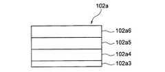
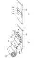
図4は、図1に示すICタグ100の矩形アンテナ2を形成する工程の一例を示す図である。また、図5は、図4に示す導電材料テープ102aの構成の一例を示す断面図である。また、図6は、図4に示す導電材料テープ102aの構成の他の例を示す断面図である。 FIG. 4 is a diagram showing an example of a process for forming the
先ず、図4(a)に示すように、第1の基材1を含む基材101を準備する。そして、案内手段10により、導電材料テープ102aを基材101の表面近傍に案内する。 First, as shown to Fig.4 (a), the
ここで、導電材料テープ102aは、例えば、図5に示すように、接着膜102a1と、導体膜102a2と、を含む。なお、接着膜102a1は、図1ないし図3に示すICタグ100の接着膜7になる。また、接着膜102a1は、導体膜102a2の一方の面(下面)に設けられ、熱可塑性接着剤で構成されている。この導体膜102a2は、図1ないし図3に示すICタグ100の矩形アンテナ2の導電膜になる。 Here, the
次に、図4(b)に示すように、導電材料テープ102aの所定の長さの部分を、熱圧着機20を用いて、熱圧着により第1の基材1に固定する。すなわち、導電材料テープ102aの接着膜102a1と第1の基材1とが接した状態で、該熱圧着により、第1の基材1と導体膜102a2とが接着膜102a1で固定される。 Next, as shown in FIG. 4B, a predetermined length portion of the
その後、導電材料テープ102aの固定されていない部分を、断裁機30を用いて断裁する。さらに、除去装置40により、裁断された導電材料テープ102aの不要部分を吸引除去する。 Thereafter, the unfixed portion of the
これにより、図4(c)に示すように、矩形アンテナ2を第1の基材1上に形成することができる。なお、図4の例では、第1の基板1上に形成された矩形アンテナ2の幅方向の側面が、断裁された部分2aである。しかし、第1の基板1上に形成された矩形アンテナ2の長手方向の側面を断裁するようにしてもよい。 Thereby, as shown in FIG. 4C, the
以上の工程により、リール102に収納された帯状の導電材料テープ102aから、第1の基材1上に矩形アンテナ2を形成する。 Through the above steps, the
そして、このようにして得られた矩形アンテナ2が表面に形成された第1の基材1と、ループアンテナ2が表面に形成された第2の基材6とを、層間膜5により接着する。すなわち、ループアンテナ2を、層間膜5を介して矩形アンテナ2の上方に配置することにより、図1ないし図3に示すICタグ100が完成する。 Then, the
以上のように、第1の基板1上に矩形アンテナ2を、既述の従来技術と比較して、容易に形成することができる。 As described above, the
なお、図4(b)に示す矩形アンテナ2の形成工程において、熱圧着工程と断裁工程とを入れ替えてもよい。すなわち、導電材料テープ102aの所定の長さの部分を断裁した後、断裁された所定の長さの部分を、熱圧着により第1の基材1に固定する。これにより、図4(c)に示すように、矩形アンテナ2を第1の基材1上に形成するようにしてもよい。 In addition, in the formation process of the
また、導電材料テープ102aは、図6に示すように、接着膜102a3、導体膜102a4、剥離層102a5、およびフィルム102a6が順次積層された積層構造を、含むようにしてもよい。なお、接着膜102a3は、熱可塑性接着剤で構成される。 Further, as shown in FIG. 6, the
この場合、接着膜102a3と第1の基材1とが接した状態で、該熱圧着により、剥離層102a5が熱により導体膜102a4から剥離するとともに、第1の基材1と導体膜102a4とが接着膜102a3で固定される(図4(c))。なお、接着膜102a3は、図1ないし図3に示すICタグ100の接着膜7になる。また、導体膜102a4は、図1ないし図3に示すICタグ100の矩形アンテナ2の導電膜になる。 In this case, while the adhesive film 102a3 and the
次に、ICタグ100の製造方法の他の例について説明する。
図7は、図1に示すICタグ100の矩形アンテナ2を形成する工程の他の例を示す図である。Next, another example of the manufacturing method of the
FIG. 7 is a diagram showing another example of the process of forming the
先ず、図7(a)に示すように、第1の基材1を含む基材101を準備する。そして、送り手段50a、50bにより導電材料テープ202aを送りつつ、案内手段60により導電材料テープ202aを基材101の表面近傍に案内する。ここで、導電材料テープ202aは、例えば、既述の図5に示すように、接着膜と、導体膜と、を含む。 First, as shown to Fig.7 (a), the
次に、導電材料テープ202aの所定の長さの部分を、断裁機70を用いて断裁する。 Next, a portion of a predetermined length of the
次に、断裁した導電材料テープ202aを熱圧着により第1の基材1に固定する。すなわち、該熱圧着により、第1の基材1と導電材料テープ202aの導体膜とが、導電材料テープ202aの接着膜で、固定される。 Next, the cut
これにより、矩形アンテナ2を第1の基材1上に形成することができる(図7(b))。 Thereby, the
以上の工程により、リール202に収納された帯状の導電材料テープ202aから、第1の基材1上に矩形アンテナ2を形成する。 Through the above steps, the
そして、このようにして得られた矩形アンテナ2が表面に形成された第1の基材1と、ループアンテナ2が表面に形成された第2の基材6とを、層間膜5により接着する。すなわち、ループアンテナ2を、層間膜5を介して矩形アンテナ2の上方に配置することにより、図1ないし図3に示すICタグ100が完成する。 Then, the
以上のように、第1の基板1上に矩形アンテナ2を、既述の従来技術と比較して、容易に形成することができる。 As described above, the
なお、図7の例では、第1の基板1上に形成された矩形アンテナ2の長手方向の側面が、断裁された部分2bである。すなわち、図7の例は、図4に示すような幅方向の側面を断裁する場合と比較して、例えば、導電材料テープの送り速度が同じ場合、スループットを向上することができる。 In the example of FIG. 7, the side surface in the longitudinal direction of the
このように、第1の基板1上に矩形アンテナ2を、既述の従来技術と比較して、容易に形成することができる。 As described above, the
すなわち、以上のように、本実施例に係るICタグおよびICタグの製造方法によれば、製造コストを低減することができる。 That is, as described above, according to the IC tag and the IC tag manufacturing method according to the present embodiment, the manufacturing cost can be reduced.
1 第1の基材(矩形アンテナ用基材)
2 矩形アンテナ
断裁された部分 2a、2b
3 ループアンテナ
3a1、3a2 第1の辺
3b1、3b2 第2の辺
4 ICチップ
5 層間膜
6 第2の基材(ループアンテナ用基材)
10 案内手段
20 熱圧着機
30、70 断裁機
40 除去装置
50 送り手段
60 案内手段
100 ICタグ
101 基材
102、202 リール
102a、202a 導電材料テープ1 1st base material (base material for rectangular antennas)
2 Rectangular antenna trimmed
3 Loop antenna 3a1, 3a2 First side 3b1, 3b2
DESCRIPTION OF
Claims (6)
Translated fromJapanese第1の基材を準備する工程と、
帯状の導電材料テープから、前記第1の基材上に前記矩形アンテナを形成する工程と、
前記ループアンテナを、前記層間膜を介して矩形アンテナの上方に配置する工程と、を備え、
前記導電材料テープの所定の長さの部分を熱圧着により前記第1の基材に固定後、前記導電材料テープの固定されていない部分を断裁することにより、前記矩形アンテナを前記第1の基材上に形成する
ことを特徴とするICタグの製造方法。A first base material, a rectangular antenna provided on the first base material and having a rectangular shape extending in a longitudinal direction, a loop antenna provided above the rectangular antenna and having a loop shape; An IC tag manufacturing method comprising: an IC chip electrically connected to the loop antenna; and an interlayer film formed between the rectangular antenna and the loop antenna,
Preparing a first substrate;
Forming a rectangular antenna on the first base material from a strip-shaped conductive material tape;
Arranging the loop antenna above the rectangular antenna via the interlayer film, and
After fixing the portion of the conductive material tape having a predetermined length to the first base member by thermocompression bonding, the portion of the conductive material tape that is not fixed is trimmed to thereby cut the rectangular antenna into the first base. A method for producing an IC tag, characterizedby beingformed on a material .
ことを特徴とする請求項1に記載のICタグの製造方法。After cutting the predetermined length portion of the conductive material tape, the cut predetermined length portion is fixed to the first base member by thermocompression bonding, whereby the rectangular antenna is fixed to the first antenna. The IC tag manufacturing method according to claim1 , wherein the IC tag is formed on a base material.
前記接着膜と前記第1の基材とが接した状態で、前記熱圧着により、前記第1の基材と前記導体膜とが前記接着膜で固定される
ことを特徴とする請求項1または2に記載のICタグの製造方法。The conductive material tape includes a conductor film, and an adhesive film provided on one surface of the conductor film and configured with a thermoplastic adhesive,
Wherein in a state where the adhesive film and the first substrate is in contact, by the thermal compression bonding, according to claim1 wherein the first base member and said conductive film is characterized in that it is fixed by the adhesive layer or2. A method for producing an IC tag according to2 .
前記接着膜は、熱可塑性接着剤で構成され、
前記接着膜と前記第1の基材とが接した状態で、前記熱圧着により、前記剥離層から熱により前記導体膜が剥離するとともに、前記第1の基材と前記導体膜とが前記接着膜で固定される
ことを特徴とする請求項1または2に記載のICタグの製造方法。The conductive material tape includes a laminated structure in which an adhesive film, a conductive film, a release layer, and a film are sequentially laminated,
The adhesive film is composed of a thermoplastic adhesive,
While the adhesive film and the first base material are in contact with each other, the conductor film is peeled off from the release layer by heat by the thermocompression bonding, and the first base material and the conductor film are bonded together. method for producing the IC tag according to claim1 or2, characterized in that it is fixed in the film.
Priority Applications (1)
| Application Number | Priority Date | Filing Date | Title |
|---|---|---|---|
| JP2009270388AJP5376321B2 (en) | 2009-11-27 | 2009-11-27 | IC tag and method of manufacturing IC tag |
Applications Claiming Priority (1)
| Application Number | Priority Date | Filing Date | Title |
|---|---|---|---|
| JP2009270388AJP5376321B2 (en) | 2009-11-27 | 2009-11-27 | IC tag and method of manufacturing IC tag |
Publications (2)
| Publication Number | Publication Date |
|---|---|
| JP2011113380A JP2011113380A (en) | 2011-06-09 |
| JP5376321B2true JP5376321B2 (en) | 2013-12-25 |
Family
ID=44235659
Family Applications (1)
| Application Number | Title | Priority Date | Filing Date |
|---|---|---|---|
| JP2009270388AActiveJP5376321B2 (en) | 2009-11-27 | 2009-11-27 | IC tag and method of manufacturing IC tag |
Country Status (1)
| Country | Link |
|---|---|
| JP (1) | JP5376321B2 (en) |
Families Citing this family (3)
| Publication number | Priority date | Publication date | Assignee | Title |
|---|---|---|---|---|
| JP6041666B2 (en)* | 2012-12-27 | 2016-12-14 | アピックヤマダ株式会社 | RFID tag, RFID tag manufacturing method, mold |
| KR101313800B1 (en) | 2013-05-02 | 2013-10-01 | 주식회사 아이디에이치 | Water supply and sewerage pipe socket forming device and its manufacturing method |
| JP5993505B2 (en)* | 2015-08-27 | 2016-09-14 | トッパン・フォームズ株式会社 | Non-contact data transmitter / receiver |
Family Cites Families (7)
| Publication number | Priority date | Publication date | Assignee | Title |
|---|---|---|---|---|
| JP2002352206A (en)* | 2001-05-30 | 2002-12-06 | Toppan Forms Co Ltd | Manufacturing method of data transceiver |
| JP2004220304A (en)* | 2003-01-15 | 2004-08-05 | Toppan Printing Co Ltd | Method of forming antenna for wireless tag and wireless tag |
| JP4694115B2 (en)* | 2003-08-14 | 2011-06-08 | 大日本印刷株式会社 | Manufacturing method of sheet with non-contact IC tag |
| JP2008197714A (en)* | 2007-02-08 | 2008-08-28 | Dainippon Printing Co Ltd | Non-contact data carrier device and auxiliary antenna for non-contact data carrier |
| EP3002820B1 (en)* | 2007-08-02 | 2020-06-03 | University of Pittsburgh - Of the Commonwealth System of Higher Education | Wireless systems having multiple electronic devices and employing simplified fabrication and matching, and associated methods |
| JP2009111950A (en)* | 2007-11-01 | 2009-05-21 | Dainippon Printing Co Ltd | Non-contact type IC tag and method of manufacturing non-contact type IC tag |
| JP5098587B2 (en)* | 2007-11-16 | 2012-12-12 | 大日本印刷株式会社 | Non-contact type IC tag and method of manufacturing non-contact type IC tag |
- 2009
- 2009-11-27JPJP2009270388Apatent/JP5376321B2/enactiveActive
Also Published As
| Publication number | Publication date |
|---|---|
| JP2011113380A (en) | 2011-06-09 |
Similar Documents
| Publication | Publication Date | Title |
|---|---|---|
| TWI267788B (en) | Radio frequency identification (RFID) tag and manufacturing method thereof | |
| TWI423519B (en) | Radio frequency identification tag | |
| CN101142711B (en) | RFID label suitable for metal and RFID label section of the same | |
| KR100679502B1 (en) | RDF tag, antenna for RDF tag, antenna sheet for RDF tag, and RDF tag manufacturing method | |
| US7126482B2 (en) | RFID tag and its manufacturing method | |
| JP5865489B2 (en) | Wire capacitor, particularly a wire capacitor for radio frequency circuits, and an apparatus comprising the wire capacitor | |
| JP5447515B2 (en) | Wireless IC device and manufacturing method thereof | |
| JP5904316B1 (en) | Carrier tape, method for manufacturing the same, and method for manufacturing RFID tag | |
| JP2009111950A (en) | Non-contact type IC tag and method of manufacturing non-contact type IC tag | |
| KR20080064728A (en) | IC chip mounting connector, antenna circuit, IC inlet, IC tag and capacitance adjustment method | |
| JP5376321B2 (en) | IC tag and method of manufacturing IC tag | |
| JP6872266B2 (en) | RF tag antenna, RF tag and RF tag antenna manufacturing method | |
| JP4802630B2 (en) | Non-contact type data carrier inlet manufacturing method, non-contact type data carrier inlet roll manufacturing method, and non-contact type data carrier manufacturing method | |
| CN109074507B (en) | Carrier tape, method for manufacturing carrier tape, and method for manufacturing RFID tag | |
| JP2014096125A (en) | Method of manufacturing non-contact communication medium, non-contact communication medium, and method of connecting antenna and circuit device | |
| JP5098588B2 (en) | Non-contact type IC tag and method of manufacturing non-contact type IC tag | |
| JP5886174B2 (en) | Non-contact communication medium manufacturing method, non-contact communication medium, and antenna and circuit device connection method | |
| JP6091848B2 (en) | Non-contact communication medium manufacturing method, non-contact communication medium, and antenna and circuit device connection method | |
| JP4930755B2 (en) | Data carrier carrier tape | |
| JP2015228234A (en) | Manufacturing method of non-contact communication medium, and connection method of antenna and circuit device | |
| JP6554899B2 (en) | Contactless communication inlay | |
| JP2020162104A (en) | IC tag | |
| JP6040732B2 (en) | IC card manufacturing method | |
| JP2010233057A (en) | Antenna circuit, ic inlet, ic tag, and capacitance adjusting method for antenna circuit | |
| JP6091849B2 (en) | Non-contact communication medium manufacturing method, non-contact communication medium, and antenna and circuit device connection method |
Legal Events
| Date | Code | Title | Description |
|---|---|---|---|
| A621 | Written request for application examination | Free format text:JAPANESE INTERMEDIATE CODE: A621 Effective date:20120918 | |
| A977 | Report on retrieval | Free format text:JAPANESE INTERMEDIATE CODE: A971007 Effective date:20130613 | |
| A131 | Notification of reasons for refusal | Free format text:JAPANESE INTERMEDIATE CODE: A131 Effective date:20130621 | |
| A521 | Written amendment | Free format text:JAPANESE INTERMEDIATE CODE: A523 Effective date:20130730 | |
| TRDD | Decision of grant or rejection written | ||
| A01 | Written decision to grant a patent or to grant a registration (utility model) | Free format text:JAPANESE INTERMEDIATE CODE: A01 Effective date:20130830 | |
| A61 | First payment of annual fees (during grant procedure) | Free format text:JAPANESE INTERMEDIATE CODE: A61 Effective date:20130912 | |
| R150 | Certificate of patent or registration of utility model | Ref document number:5376321 Country of ref document:JP Free format text:JAPANESE INTERMEDIATE CODE: R150 Free format text:JAPANESE INTERMEDIATE CODE: R150 |