JP5371238B2 - Plasma processing apparatus and plasma processing method - Google Patents
Plasma processing apparatus and plasma processing methodDownload PDFInfo
- Publication number
- JP5371238B2 JP5371238B2JP2007328335AJP2007328335AJP5371238B2JP 5371238 B2JP5371238 B2JP 5371238B2JP 2007328335 AJP2007328335 AJP 2007328335AJP 2007328335 AJP2007328335 AJP 2007328335AJP 5371238 B2JP5371238 B2JP 5371238B2
- Authority
- JP
- Japan
- Prior art keywords
- frequency
- electrode
- frequency power
- power
- plasma processing
- Prior art date
- Legal status (The legal status is an assumption and is not a legal conclusion. Google has not performed a legal analysis and makes no representation as to the accuracy of the status listed.)
- Expired - Fee Related
Links
Images


Classifications
- H—ELECTRICITY
- H01—ELECTRIC ELEMENTS
- H01J—ELECTRIC DISCHARGE TUBES OR DISCHARGE LAMPS
- H01J37/00—Discharge tubes with provision for introducing objects or material to be exposed to the discharge, e.g. for the purpose of examination or processing thereof
- H01J37/32—Gas-filled discharge tubes
- H01J37/32009—Arrangements for generation of plasma specially adapted for examination or treatment of objects, e.g. plasma sources
- H01J37/32082—Radio frequency generated discharge
- H01J37/32137—Radio frequency generated discharge controlling of the discharge by modulation of energy
- H01J37/32155—Frequency modulation
- H01J37/32165—Plural frequencies
- H—ELECTRICITY
- H01—ELECTRIC ELEMENTS
- H01J—ELECTRIC DISCHARGE TUBES OR DISCHARGE LAMPS
- H01J37/00—Discharge tubes with provision for introducing objects or material to be exposed to the discharge, e.g. for the purpose of examination or processing thereof
- H01J37/32—Gas-filled discharge tubes
- H01J37/32009—Arrangements for generation of plasma specially adapted for examination or treatment of objects, e.g. plasma sources
- H01J37/32082—Radio frequency generated discharge
- H01J37/32174—Circuits specially adapted for controlling the RF discharge
- H01J37/32183—Matching circuits
- H—ELECTRICITY
- H01—ELECTRIC ELEMENTS
- H01J—ELECTRIC DISCHARGE TUBES OR DISCHARGE LAMPS
- H01J37/00—Discharge tubes with provision for introducing objects or material to be exposed to the discharge, e.g. for the purpose of examination or processing thereof
- H01J37/32—Gas-filled discharge tubes
- H01J37/32431—Constructional details of the reactor
- H01J37/3244—Gas supply means
- H—ELECTRICITY
- H01—ELECTRIC ELEMENTS
- H01J—ELECTRIC DISCHARGE TUBES OR DISCHARGE LAMPS
- H01J37/00—Discharge tubes with provision for introducing objects or material to be exposed to the discharge, e.g. for the purpose of examination or processing thereof
- H01J37/32—Gas-filled discharge tubes
- H01J37/32431—Constructional details of the reactor
- H01J37/32458—Vessel
- H—ELECTRICITY
- H01—ELECTRIC ELEMENTS
- H01J—ELECTRIC DISCHARGE TUBES OR DISCHARGE LAMPS
- H01J37/00—Discharge tubes with provision for introducing objects or material to be exposed to the discharge, e.g. for the purpose of examination or processing thereof
- H01J37/32—Gas-filled discharge tubes
- H01J37/32431—Constructional details of the reactor
- H01J37/32532—Electrodes
- H—ELECTRICITY
- H01—ELECTRIC ELEMENTS
- H01J—ELECTRIC DISCHARGE TUBES OR DISCHARGE LAMPS
- H01J37/00—Discharge tubes with provision for introducing objects or material to be exposed to the discharge, e.g. for the purpose of examination or processing thereof
- H01J37/32—Gas-filled discharge tubes
- H01J37/32431—Constructional details of the reactor
- H01J37/32798—Further details of plasma apparatus not provided for in groups H01J37/3244 - H01J37/32788; special provisions for cleaning or maintenance of the apparatus
- H01J37/32816—Pressure
- H01J37/32834—Exhausting
- H—ELECTRICITY
- H05—ELECTRIC TECHNIQUES NOT OTHERWISE PROVIDED FOR
- H05H—PLASMA TECHNIQUE; PRODUCTION OF ACCELERATED ELECTRICALLY-CHARGED PARTICLES OR OF NEUTRONS; PRODUCTION OR ACCELERATION OF NEUTRAL MOLECULAR OR ATOMIC BEAMS
- H05H1/00—Generating plasma; Handling plasma
- H05H1/24—Generating plasma
- H05H1/46—Generating plasma using applied electromagnetic fields, e.g. high frequency or microwave energy
- H05H1/4645—Radiofrequency discharges
- H05H1/4652—Radiofrequency discharges using inductive coupling means, e.g. coils
- H—ELECTRICITY
- H01—ELECTRIC ELEMENTS
- H01J—ELECTRIC DISCHARGE TUBES OR DISCHARGE LAMPS
- H01J2237/00—Discharge tubes exposing object to beam, e.g. for analysis treatment, etching, imaging
- H01J2237/32—Processing objects by plasma generation
- H01J2237/33—Processing objects by plasma generation characterised by the type of processing
- H01J2237/332—Coating
- H—ELECTRICITY
- H01—ELECTRIC ELEMENTS
- H01J—ELECTRIC DISCHARGE TUBES OR DISCHARGE LAMPS
- H01J2237/00—Discharge tubes exposing object to beam, e.g. for analysis treatment, etching, imaging
- H01J2237/32—Processing objects by plasma generation
- H01J2237/33—Processing objects by plasma generation characterised by the type of processing
- H01J2237/334—Etching
- H—ELECTRICITY
- H05—ELECTRIC TECHNIQUES NOT OTHERWISE PROVIDED FOR
- H05H—PLASMA TECHNIQUE; PRODUCTION OF ACCELERATED ELECTRICALLY-CHARGED PARTICLES OR OF NEUTRONS; PRODUCTION OR ACCELERATION OF NEUTRAL MOLECULAR OR ATOMIC BEAMS
- H05H2242/00—Auxiliary systems
- H05H2242/20—Power circuits
Landscapes
- Physics & Mathematics (AREA)
- Engineering & Computer Science (AREA)
- Plasma & Fusion (AREA)
- Chemical & Material Sciences (AREA)
- Analytical Chemistry (AREA)
- Electromagnetism (AREA)
- Spectroscopy & Molecular Physics (AREA)
- Plasma Technology (AREA)
- Drying Of Semiconductors (AREA)
Description
Translated fromJapanese本発明は、フラットパネルディスプレイ(FPD)製造用のガラス基板などの基板に対してドライエッチング等のプラズマを施すプラズマ処理装置およびプラズマ処理方法に関する。 The present invention relates to a plasma processing apparatus and a plasma processing method for performing plasma such as dry etching on a substrate such as a glass substrate for manufacturing a flat panel display (FPD).
例えば、FPDの製造プロセスや半導体デバイスの製造プロセスにおいては、ガラス基板や半導体ウエハ等の基板に対して、ドライエッチング等のプラズマ処理が行われる。このようなプラズマ処理には、平行平板型のプラズマ処理装置が多用されている。 For example, in an FPD manufacturing process or a semiconductor device manufacturing process, plasma processing such as dry etching is performed on a substrate such as a glass substrate or a semiconductor wafer. For such plasma processing, a parallel plate type plasma processing apparatus is frequently used.
平行平板型のプラズマ処理装置は、チャンバ内に基板を載置する載置台と処理ガスをシャワー状に供給するシャワーヘッドとを相対向するように設け、載置台を下部電極として機能させ、シャワーヘッドを上部電極として機能させて、これらの少なくとも一方に高周波電力を印加することにより、これらの間に高周波電界を形成し、この高周波電界により処理ガスをプラズマ化してガラス基板に対してプラズマ処理を行う。 A parallel plate type plasma processing apparatus is provided with a mounting table for mounting a substrate in a chamber and a shower head for supplying a processing gas in a shower-like manner so that the mounting table functions as a lower electrode. Is made to function as an upper electrode, and a high frequency electric field is applied to at least one of them to form a high frequency electric field between them, and a plasma treatment is performed on the glass substrate by converting the processing gas into plasma by this high frequency electric field. .
このような平行平板型プラズマ処理装置をプラズマエッチング装置として適用する場合には、上部電極であるシャワーヘッドに相対的に周波数の高い第1の高周波電力を印加し、下部電極である載置台に相対的に周波数の低い第2の高周波電力を印加する上部下部印加タイプや、下部電極である載置台に相対的に周波数の高い第1の高周波電力と相対的に周波数の低い第2の高周波電力を印加する下部2周波印加タイプなども用いられ、このような構成によりプラズマを適切に制御して良好なエッチング処理が行われている。 When such a parallel plate type plasma processing apparatus is applied as a plasma etching apparatus, a first high frequency power having a relatively high frequency is applied to a shower head which is an upper electrode, and a relative to a mounting table which is a lower electrode. In particular, an upper / lower application type that applies a second high-frequency power having a low frequency or a first high-frequency power having a relatively high frequency and a second high-frequency power having a relatively low frequency are applied to a mounting table that is a lower electrode. A lower two-frequency application type to be applied is also used, and a favorable etching process is performed by appropriately controlling plasma with such a configuration.
ところで、このような上部下部印加タイプや下部2周波印加タイプを含めた平行平板型プラズマ処理装置は、放電条件によっては、上部電極であるシャワーヘッドのガス吐出孔内にアーク放電が発生し、シャワーヘッド(シャワーヘッドが保持する電極板)が損傷して寿命が短くなったりデバイス欠陥をもたらしたりすることがある。 By the way, in such a parallel plate type plasma processing apparatus including the upper lower application type and the lower two frequency application type, depending on discharge conditions, arc discharge occurs in the gas discharge hole of the shower head which is the upper electrode, and the shower is performed. The head (electrode plate held by the shower head) may be damaged to shorten the life or cause a device defect.
それを解決する技術として、特許文献1には上部電極に相対的に周波数の低い第2の高周波電力を印加して、上部電極のプラズマシースを厚くして、プラズマがシャワーヘッドのガス吐出孔内に侵入することを妨げる技術が提案されている。 As a technique for solving this problem,
しかしながら、この種の平行平板型プラズマ処理装置には、このような異常放電にともなう問題だけではなく、上部電極に付着する反応性生成物が原因となるデバイスの欠陥が発生し歩留まりが低下するという問題や、このような反応生成物を除去するためにメンテナンスサイクルが短くなりスループットが低下するという問題がある。
本発明はかかる事情に鑑みてなされたものであって、異常放電による問題が生じず、かつ電極に付着する反応生成物に起因する問題を解消することができる平行平板型のプラズマ処理装置およびプラズマ処理方法を提供することを目的とする。 The present invention has been made in view of such circumstances, and a parallel plate type plasma processing apparatus and a plasma that are free from problems caused by abnormal discharge and that can solve problems caused by reaction products adhering to electrodes. An object is to provide a processing method.
上記課題を解決するため、本発明の第1の観点では、被処理基板が収容される処理室と、前記処理室内で相対向して設けられ、容量結合平行平板電極を構成する第1電極および第2電極と、前記第1電極に周波数が10MHz以上の第1の高周波電力を印加する第1の高周波電力印加手段と、前記第1電極に周波数が2MHz以上10MHz未満の第2の高周波電力を印加する第2の高周波電力印加手段と、前記第2電極に周波数が400kHz以上1.6MHz以下の第3の高周波電力を印加する第3の高周波電力印加手段と、前記処理室内にプラズマ生成のための処理ガスを供給するガス供給機構と、前記処理室を排気する排気機構とを具備し、前記第1電極は被処理基板を支持する支持電極であり、前記第2電極は前記支持電極に対向して設けられた対向電極であり、前記第3の高周波電力は、前記第1および第2の高周波電力と干渉しないように、その周波数は、前記第1および第2の高周波電力の周波数がその整数倍とならないような周波数であることを特徴とするプラズマ処理装置を提供する。In order to solve the above problems, according to a first aspect of the present invention, a processing chamber in which a substrate to be processed is accommodated, a first electrode that is provided opposite to each other in the processing chamber, and constitutes a capacitively coupled parallel plate electrode; A second high-frequency power applying means for applying a first high-frequency power having a frequency of 10 MHz or more to the first electrode; and a second high-frequency power having a frequency of not less than 2 MHz but less than 10 MHz to the first electrode. A second high frequency power applying means for applying; a third high frequency power applying means for applying a third high frequency power having a frequency of 400 kHz to 1.6 MHz to the second electrode; and for generating plasma in the processing chamber. A gas supply mechanism for supplying the processing gas and an exhaust mechanism for exhausting the processing chamber, wherein the first electrode is a support electrode for supporting the substrate to be processed, and the second electrode is opposed to the support electrode. A counter electrode provided Te, the third high frequency power, the first andso as not to interfere with the second high frequency powerwhose frequency is the frequency of the first and second high-frequency power that integer Provided is a plasma processing apparatus havinga frequency that does not double .
上記第1の観点において、前記第3の高周波電力は、前記第1または第2電極に付着した付着物を十分に除去することができ付着物が付着しない程度で、かつ前記第2電極を消耗させ難いパワーに設定することが好ましい。具体的なパワーとしては0.009〜0.055W/cm2の範囲が好ましい。また、前記第3の高周波電力のより好ましい周波数の範囲としては、600kHz以上1.0MHz以下の範囲を挙げることができる。TheTe first aspectodor, before Symbol third high frequency power, the first or extent deposits do not adhere can be sufficiently removed the extraneous matters adhered to the second electrode, and the second electrode It is preferable to set the power so that it is difficult to consume. The specific power is preferably in the range of 0.009 to 0.055 W / cm2 . Moreover, as a more preferable frequency range of the third high frequency power, a range of 600 kHz to 1.0 MHz can be exemplified.
また、前記第2の電極に接続され、前記第1の高周波電力の周波数に対しては低インピーダンスであり、前記第2の高周波電力の周波数および前記第3の高周波電力の周波数に対しては高インピーダンスになるようにインピーダンス調整された第1のインピーダンス調整器と、前記第2の電極に接続され、前記第2の高周波電力の周波数に対しては低インピーダンスであり、前記第1の高周波電力の周波数および前記第3の高周波電力の周波数に対しては高インピーダンスになるようにインピーダンス調整された第2のインピーダンス調整器とをさらに具備する構成とすることができる。この場合に、前記処理室の側壁に接続され、前記第3の高周波電力の周波数に対しては低インピーダンスであり、前記第1の高周波電力の周波数および前記第2の高周波電力の周波数に対しては高インピーダンスになるようにインピーダンス調整された第3のインピーダンス調整器をさらに具備するようにすることもできる。
被処理基板として絶縁性の基板を用いることができる。In addition, it is connected to the second electrode and has alow impedance with respect to the frequency of the first high-frequency power, and is high with respect tothe frequency of the second high-frequency power and the frequency of the thirdhigh-frequency power. A first impedance adjuster having an impedance adjusted so as to have an impedance; and the second electrode, the impedance beinglow with respect to the frequency of the second high-frequency power, and the first high-frequency power A second impedance adjuster that is impedance-adjusted to have a high impedance with respect to the frequency and the frequency of the thirdhigh-frequency power can be further provided. In this case, it is connected to the side wall of the processing chamber and has alow impedance with respect to the frequency of the third high-frequency power, and with respect to the frequency of the first high-frequency power and the frequency of the secondhigh-frequency power . Can further comprise a third impedance adjuster that is impedance adjusted to be high impedance.
An insulating substrate can be used as the substrate to be processed.
本発明の第2の観点では、被処理基板が収容される処理室で相対向して容量結合平行平板電極を構成する第1電極および第2電極を設け、これらの間に高周波電界を形成し、この高周波電界により処理ガスをプラズマ化して被処理基板にプラズマ処理を施すプラズマ処理方法であって、前記第1電極を被処理基板を支持する支持電極とし、前記第2電極を前記支持電極に対向して設けられた対向電極として、前記第1電極に周波数が10MHz以上の第1の高周波電力と周波数が2MHz以上10MHz未満の第2の高周波電力を印加してプラズマを生成し、前記第2電極に、400kHz以上1.6MHz以下の範囲であり、かつ前記第1および第2の高周波電力と干渉しないように、前記第1および第2の高周波電力の周波数がその整数倍とならないような周波数である第3の高周波電力を印加して前記第1電極または前記第2電極の表面をスパッタしてクリーニングすることを特徴とするプラズマ処理方法を提供する。In a second aspect of the present invention, the first electrode and the second electrode constituting the capacitive coupling parallel-plate electrodes to face the processing chamber substrateto be processed is accommodated is provided, the high frequency electric field is formed between the A plasma processing method for converting a processing gas into plasma by this high-frequency electric field and performing plasma processing on thesubstrate tobe processed , wherein the first electrode is a supporting electrode that supports the substrate to be processed, and the second electrode is used as the supporting electrode. As a counter electrode provided oppositely, a plasma is generated by applying a first high-frequency power having a frequency of 10 MHz or more and a second high-frequency power having a frequency of 2 MHz or more and less than 10 MHz to the first electrode, and generating the second the electrode, a 1.6MHz following range of 400kHz, and the first andso as not to interfere with the second high-frequencypower, frequency of the first and second high-frequency power that integer By sputtering the surface of the third high-frequency power is applied to the first electrode or the second electrodeis a frequency such as not to provide a plasma processing method characterized by cleaning.
上記第2の観点において、前記第3の高周波電力は、前記第1または第2電極に付着した付着物を十分に除去することができ付着物が付着しない程度で、かつ前記第2電極を消耗させ難いパワーに設定することが好ましい。具体的なパワーとしては0.009〜0.055W/cm2の範囲が好ましい。また、前記第3の高周波電力のより好ましい周波数の範囲としては、600kHz以上1.0MHz以下の範囲を挙げることができる。
被処理基板として絶縁性の基板を用いることができる。TheTe second aspectodor, before Symbol third high frequency power, the first or extent deposits do not adhere can be sufficiently removed the extraneous matters adhered to the second electrode, and the second electrode It is preferable to set the power so that it is difficult to consume. The specific power is preferably in the range of 0.009 to 0.055 W / cm2 . Moreover, as a more preferable frequency range of the third high frequency power, a range of 600 kHz to 1.0 MHz can be exemplified.
An insulating substrate can be used as the substrate to be processed.
本発明によれば、第1の高周波電力を第1電極または第2電極に印加し、第2の高周波電力を第1電極に印加することにより、プラズマシースが広がって異常放電を生じ難くすることができ、また、第3の高周波電力を第2電極に印加することにより、そのスパッタ効果により、第1または第2電極、典型的には上部電極の表面をクリーニングすることができる。
According to the present invention,the first high-frequency power is applied to the first electrode or the second electrode, and the second high-frequency power is applied to the first electrode, so that the plasma sheath spreads and abnormal discharge is hardly caused. In addition, by applying the third high-frequency power to the second electrode, the surface of the first or second electrode, typically the upper electrode, can be cleaned by the sputtering effect.
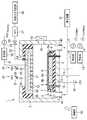
以下、添付図面を参照して、本発明の実施形態について説明する。図1は、本発明の一実施形態に係るプラズマ処理装置を示す断面図である。このプラズマ処理装置1は、FPD用ガラス基板Gの所定の膜をプラズマエッチングする容量結合型平行平板プラズマエッチング装置として構成されている。ここで、FPDとしては、液晶ディスプレイ(LCD)、エレクトロルミネセンス(Electro Luminescence;EL)ディスプレイ、プラズマディスプレイパネル(PDP)等が例示される。 Embodiments of the present invention will be described below with reference to the accompanying drawings. FIG. 1 is a cross-sectional view showing a plasma processing apparatus according to an embodiment of the present invention. The
このプラズマ処理装置1は、例えば表面がアルマイト処理(陽極酸化処理)されたアルミニウムからなる角筒形状に成形された処理チャンバ2を有している。この処理チャンバ2内の底部には被処理基板であるガラス基板Gを載置するための載置台3が設けられている。 The
載置台3は、絶縁部材4を介して処理チャンバ2の底部に支持されており、金属製の凸型の基材5と基材5の凸部5aの上に設けられたガラス基板Gを吸着する静電チャック6と、静電チャック6および基材5の凸部5aの周囲に設けられた、絶縁性セラミックス、例えばアルミナからなる額縁状のシールドリング7と、基材5の周囲に設けられた絶縁性セラミックス、例えばアルミナからなるリング状の絶縁リング8とを有している。静電チャック6はセラミックス等の誘電体からなる本体6a中に電極6bが埋設されて構成されている。電極6bには給電線18が接続されており、給電線18には直流電源19が接続されていて、電極6bに直流電源19からの直流電圧が印加されることにより、クーロン力等の静電吸着力によりガラス基板Gが吸着される。 The mounting table 3 is supported on the bottom of the
処理チャンバ2の底壁、絶縁部材4および載置台3を貫通するように、その上へのガラス基板Gのローディングおよびアンローディングを行うための昇降ピン10が昇降可能に挿通されている。この昇降ピン10はガラス基板Gを搬送する際には、載置台3の上方の搬送位置まで上昇され、それ以外のときには載置台3内に没した状態となる。 Lifting
載置台3の基材5には、第1の高周波電力を供給するための給電線12が接続されており、この給電線12には第1の整合器13および第1の高周波電源14が接続されている。第1の高周波電源14からは10MHz以上、例えば13.56MHzの第1の高周波電力が載置台3の基材5に供給される。また、基材5には、第2の高周波電力を供給するための給電線15が接続されており、この給電線15には第2の整合器16および第2の高周波電源17が接続されている。第2の高周波電源17からは2MHz以上10MHz未満、例えば3.2MHzの第2の高周波電力が載置台3の基材5に供給される。したがって、載置台3は下部電極として機能する。 A
前記載置台3の上方には、この載置台3と平行に対向して上部電極として機能するシャワーヘッド20が設けられている。シャワーヘッド20は処理チャンバ2の上部に絶縁部材29を介して支持されており、内部に内部空間21を有するとともに、載置台3との対向面に処理ガスを吐出する複数のガス吐出孔22が形成されている。この上部電極であるシャワーヘッド20は、下部電極である載置台3とともに一対の平行平板電極を構成している。 Above the mounting table 3, a
シャワーヘッド20の上面にはガス導入口24が設けられ、このガス導入口24には、処理ガス供給管25が接続されており、この処理ガス供給管25は処理ガス供給源28に接続されている。また、処理ガス供給管25には、開閉バルブ26およびマスフローコントローラ27が介在されている。処理ガス供給源28からは、プラズマエッチングのための処理ガスが供給される。処理ガスとしては、ハロゲン系のガス、O2ガス、Arガス等、通常この分野で用いられるガスを用いることができる。A
また、上部電極であるシャワーヘッド20には、第3の高周波電力を供給するための給電線31が接続されており、この給電線31には第3の整合器32および第3の高周波電源33が接続されている。第3の高周波電源33からは400kHz以上1.6MHz以下、例えば750kHzの第3の高周波電力が上部電極であるシャワーヘッド20に供給される。また、第3の高周波電力の周波数は、第1および第2の高周波電力の周波数と干渉しない周波数とする。すなわち、前記第3の高周波電力の周波数は、第1および第2の高周波電力の周波数の整数分の一とならないようにする。逆に言えば、第1および第2の高周波電力の周波数が第3の高周波電力の周波数の整数倍とならないようにする。 The
また、上部電極であるシャワーヘッド20の上部外側には、第1の高周波電力用の第1のインピーダンス調整器34と、第2の高周波電力用の第2のインピーダンス調整器35が接続されている。 A
第1のインピーダンス調整器34はコイル36および可変コンデンサ37が直列に接続されて構成されており、第1の高周波電力の周波数に対するインピーダンスの絶対値が低く、他の高周波電力の周波数に対するインピーダンスの絶対値が高くなるように回路定数が設定され、第1の高周波電力は流れ、第2および第3の高周波電力はほとんど流れないようになっている。 The
第2のインピーダンス調整器35は、コイル38と可変コンデンサ39が直列に接続されて構成されており、第2の高周波電力の周波数に対するインピーダンスの絶対値が低く、他の高周波電力の周波数に対するインピーダンスの絶対値が高くなるように回路定数が設定され、第2の高周波電力は流れ、第1および第3の高周波電力はほとんど流れないようになっている。The
処理チャンバ2の底部には排気管40が形成されており、この排気管40には排気装置41が接続されている。排気装置41はターボ分子ポンプなどの真空ポンプを備えており、これにより処理チャンバ2内を所定の減圧雰囲気まで真空引き可能なように構成されている。また、処理チャンバ2の側壁には基板搬入出口42が設けられており、この基板搬入出口42がゲートバルブ43により開閉可能となっている。そして、このゲートバルブ43を開にした状態で搬送装置(図示せず)によりガラス基板Gが搬入出されるようになっている。 An
このプラズマ処理装置1の各構成部は、制御部50により制御されるようになっている。この制御部50は、所定の制御を実施するための制御プログラム等を格納するプログラム格納部、制御プログラムに基づいて実際に各構成部を制御するコントローラ、およびキーボードやディスプレー等からなるユーザーインターフェースを有している。 Each component of the
具体的には、この制御部50は、各高周波電源からの高周波電力の印加のタイミング、これらのパワーの制御、ガスの供給および排気の制御、ゲートバルブ、昇降ピン等の駆動制御、静電チャックへの電圧供給制御等の制御を行う。 Specifically, the
次に、このように構成されるプラズマ処理装置1における処理動作について説明する。
まず、ゲートバルブ43を開いて、ガラス基板Gを搬送アーム(図示せず)により基板搬入出口42を介して処理チャンバ2内へと搬入し、載置台3の静電チャック6上に載置する。この場合に、昇降ピン10を上方に突出させて支持位置に位置させ、搬送アーム上のガラス基板Gを昇降ピン10の上に受け渡す。その後、昇降ピン10を下降させてガラス基板Gを載置台3の静電チャック6上に載置する。Next, the processing operation in the
First, the
その後、ゲートバルブ43を閉じ、排気装置41によって、処理チャンバ2内を所定の真空度まで真空引きする。そして、直流電源19から静電チャック6の電極6bに電圧を印加することにより、ガラス基板Gを静電吸着する。そして、バルブ26を開放して、処理ガス供給源28から処理ガスを、マスフローコントローラ27によってその流量を調整しつつ、処理ガス供給管25、ガス導入口24を通ってシャワーヘッド20の内部空間21へ導入し、さらに吐出孔22を通って基板Gに対して均一に吐出し、排気量を調節しつつ処理チャンバ2内を所定圧力に制御する。 Thereafter, the
この状態で、下部電極である載置台3の基材5に、第1の高周波電源14から第1の整合器13を介して10MHz以上、例えば13.56MHzの第1の高周波電力を供給し、第2の高周波電源17から第2の整合器16を介して2MHz以上10MHz未満、例えば3.2MHzの第2の高周波電力を供給し、下部電極としての載置台3と上部電極としてのシャワーヘッド20との間に高周波電界を生じさせて、処理ガスのプラズマを生成し、このプラズマによりガラス基板Gにプラズマエッチング処理を施す。 In this state, the first high-frequency power of 10 MHz or more, for example, 13.56 MHz, is supplied from the first high-
ここで、第1の高周波電力の周波数を10MHz以上としたのは、プラズマ中のイオンが瞬時電界に応答することができず、負の直流電圧(自己バイアス)が発生する周波数帯域であり、且つプラズマの高密度化が可能となるからである。また、第2の高周波電力の周波数を2MHz以上10MHz未満としたのは、イオンを更に加速させ、基板表面反応の促進、異方性エッチングの効果を高めるためであり、2MHz未満の低い周波数ではプラズマ中のイオンが電界の変化に追従し、自己バイアスではなくイオン衝突(スパッタリング効果)となり、基板へのダメージが強くなる懸念があるからである。 Here, the frequency of the first high-frequency power is set to 10 MHz or more in a frequency band in which ions in the plasma cannot respond to the instantaneous electric field and a negative DC voltage (self-bias) is generated, and This is because the plasma density can be increased. The reason why the frequency of the second high-frequency power is set to 2 MHz or more and less than 10 MHz is to further accelerate the ions, promote the substrate surface reaction, and enhance the effect of anisotropic etching. This is because the ions inside follow the change in the electric field and cause ion collision (sputtering effect) instead of self-bias, which may cause damage to the substrate.
このように下部電極である載置台3に第1の高周波電力および第2の高周波電力を供給してこれらを重畳させることにより、プラズマを適切に制御して良好なエッチング処理を行うことはできるが、エッチングを継続すると、上部電極であるシャワーヘッド20の表面に反応生成物が付着し、それが原因となってデバイスの欠陥が発生し歩留まりが低下するおそれがある。また、このようなデバイスの欠陥を生じさせないためにメンテナンスサイクルを短くすると装置稼働率が低下してしまう。 Thus, by supplying the first high-frequency power and the second high-frequency power to the mounting table 3 that is the lower electrode and superimposing them, it is possible to appropriately control the plasma and perform a good etching process. If the etching is continued, the reaction product adheres to the surface of the
このようなことを防止する観点から、本実施形態では、上部電極であるシャワーヘッド20に、第3の高周波電源33から第3の整合器32を介して、より低周波数である400kHz以上1.6MHz、例えば750KHzの第3の高周波電力を適切なパワーで印加する。これにより上部電極のプラズマシースを広げて積極的にシース電圧を高くし、上部電極であるシャワーヘッド20に付着する反応生成物(付着物)をイオンスパッタによりドライクリーニングすることができる。 From the viewpoint of preventing this, in the present embodiment, the
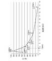
第3の高周波電力の周波数を400kHz以上1.6MHz以下の範囲にしたのは、この範囲で良好なスパッタ力を得ることができるからである。このことを確認した実験について説明する。ここでは、下部電極を上部電極と見立てて、各周波数の高周波電力を印加した下部電極の自己バイアス電圧(Vdc)を測定する実験を行い、第3の高周波電力の周波数とスパッタ力の指標である自己バイアス電圧(Vdc)との関係を求めた。その結果を図2に示す。図2は、横軸に高周波電力の周波数をとり、縦軸に自己バイアス電圧(Vdc)をとって、これらの関係について示すグラフである。このグラフから、Vdcは800kHz(0.8MHz)で極大値をとり、400kHz(0.4MHz)〜1.6MHzの範囲で600V以上の高いVdcが得られることがわかる。より好ましい範囲は、600kHz(0.6MHz)〜1.0MHzの範囲である。このような周波数の範囲から第1および第2の高周波電力の周波数と干渉しない周波数を選択する。 The reason why the frequency of the third high-frequency power is in the range of 400 kHz to 1.6 MHz is that good sputtering force can be obtained in this range. An experiment confirming this will be described. Here, the lower electrode is regarded as the upper electrode, and an experiment for measuring the self-bias voltage (Vdc) of the lower electrode to which the high frequency power of each frequency is applied is performed, which is an index of the frequency and the sputtering force of the third high frequency power. The relationship with the self-bias voltage (Vdc) was obtained. The result is shown in FIG. FIG. 2 is a graph showing the relationship between the frequency of the high frequency power on the horizontal axis and the self-bias voltage (Vdc) on the vertical axis. From this graph, it can be seen that Vdc takes a maximum value at 800 kHz (0.8 MHz), and a high Vdc of 600 V or higher is obtained in the range of 400 kHz (0.4 MHz) to 1.6 MHz. A more preferable range is 600 kHz (0.6 MHz) to 1.0 MHz. A frequency that does not interfere with the frequencies of the first and second high-frequency powers is selected from such a frequency range.
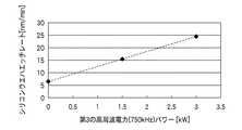
次に、第3の高周波電力のパワーとスパッタ力との関係を把握した実験について説明する。ここでは、30mm×30mmの正方形にカットしたシリコンウエハサンプルを上部電極(220cm×250cm)の図3に示すような位置に貼り付けて、下部電極に第1の高周波電力として周波数13.56MHz、パワー5kW、第2の高周波電力として周波数3.2MHz、パワー5kWの高周波電力を印加し、上部電極に第3の高周波電力として周波数750kHzの高周波電力をパワーを変化させて印加し、シリコンウエハサンプルのエッチングレートを把握した。その結果を図4に示す。図4は、横軸に第3の高周波電力(750kHz)のパワーをとり、縦軸にシリコンウエハのエッチレートの平均値との関係を示す図である。この図に示すように、第3の高周波電力を印加することによりエッチレートが上昇すること、すなわち付着物のスパッタ効果が向上することがわかる。そして、エッチレートは第3の高周波電力のパワーが増加するほど上昇することが確認された。 Next, an experiment that grasps the relationship between the power of the third high-frequency power and the sputtering force will be described. Here, a silicon wafer sample cut into a square of 30 mm × 30 mm is attached to the position of the upper electrode (220 cm × 250 cm) as shown in FIG. 3, and the frequency of 13.56 MHz as the first high-frequency power is applied to the lower electrode. Etch silicon wafer sample by applying 5 kW, high frequency power of 3.2 MHz as second high frequency power and high frequency power of 5 kW, applying high frequency power of 750 kHz as third high frequency power to the upper electrode while changing the power. I figured out the rate. The result is shown in FIG. FIG. 4 is a graph showing the relationship between the third high frequency power (750 kHz) on the horizontal axis and the average value of the etch rate of the silicon wafer on the vertical axis. As shown in this figure, it can be seen that applying the third high-frequency power increases the etch rate, that is, improves the sputtering effect of the deposit. It was confirmed that the etch rate increased as the power of the third high-frequency power increased.
このことから、反応生成物(付着物)を十分に除去することができ反応生成物の付着が生じないパワーに設定して第3の高周波電力を供給する必要がある。ただし、第3の高周波電力のパワーが大きすぎると上部電極が消耗してしまうため、このようなことが生じない適切なパワーに設定することが必要となる。第3の高周波電力のパワーの好ましい範囲は0.009〜0.055W/cm2程度である。For this reason, it is necessary to supply the third high-frequency power by setting the power so that the reaction product (adhesion) can be sufficiently removed and the reaction product does not adhere. However, since the upper electrode is consumed if the power of the third high-frequency power is too large, it is necessary to set the power to an appropriate level that does not cause this. A preferable range of the power of the third high-frequency power is about 0.009 to 0.055 W / cm2 .
この第3の高周波電力による上部電極であるシャワーヘッド20のクリーニングを行う方法として、ガラス基板Gにエッチング処理を施している際に、第1および第2の高周波電力の印加後、少し遅れて第3の高周波電力を印加して、上部電極であるシャワーヘッド20に付着した反応生成物をリアルタイムで除去し、見かけ上、反応生成物が付着しないようにすることができる。または第1および第2の高周波電力を印加してガラス基板Gのプラズマ処理を所定枚数行った後、例えばロットの変わり目等に、ダミー基板を載せた状態で、あるいは載置台に何も載せずに、第1および第2の高周波電力に加えて、第3の高周波電力を供給して上部電極であるシャワーヘッド20のクリーニングを行うようにしてもよい。なお、第1および第2の高周波電力と第3の高周波電力を同時に印加しても良い。さらに別の方法としては、クリーニングのみを行う際には第1の高周波電力と第3の高周波電力のみを供給するようにすることもできる。 As a method of cleaning the
次に、インピーダンス調整について説明する。
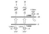
本実施形態が対象とするガラス基板は、大型化の一途をたどり、一辺が2mを超えるものとなっており、このような大型のガラス基板にプラズマ処理を行う場合には、装置も大型なものとなるため、プラズマを均一に形成することが難しく、プラズマの偏りが生じやすくなる。そこで、このようなプラズマの偏りを防止する観点から、図5にも模式的に示すように、上部電極であるシャワーヘッド20の上部外側に第1の高周波電力用の第1のインピーダンス調整器34と、第2の高周波電力用の第2のインピーダンス調整器35を設け、第1のインピーダンス調整器34は第1の高周波電力に対するインピーダンスを最適化して第1の高周波電力のみが流れるようにし、第2のインピーダンス調整器35は第2の高周波電力に対するインピーダンスを最適化して第2の高周波電力のみが流れるようにして、第1の高周波電力および第2の高周波電力を上部電極であるシャワーヘッド20へ導き、これら高周波電力に偏りが生じないようにしている。すなわち、第1のインピーダンス調整器34および第2のインピーダンス調整器35はインピーダンス調整機能の他にフィルター機能をも有する。Next, impedance adjustment will be described.
The glass substrate targeted by the present embodiment is steadily increasing in size, and one side exceeds 2 m. When performing plasma treatment on such a large glass substrate, the apparatus is also large. Therefore, it is difficult to form the plasma uniformly, and the plasma tends to be biased. Therefore, from the viewpoint of preventing such plasma bias, the
このようなインピーダンス調整器は従来から用いられているが、本実施形態では、第3の高周波電力を上部電極であるシャワーヘッド20に供給するため、第1および第2のインピーダンス調整器34,35は上記機能の他、第3の高周波電力が第1および第2のインピーダンス調整器34,35を通して接地側に流れないようにこれら第1および第2のインピーダンス調整器34,35の回路定数を設定する必要がある。すなわち、図5に示すように、第1のインピーダンス調整器34では、第1の高周波電力に対するインピーダンスを最適化し、第2および第3の高周波電力に対するインピーダンスの絶対値が高くなるように回路定数を設定して、ほぼ第1の高周波電力のみが流れるようにし、第2のインピーダンス調整器35では、第2の高周波電力に対するインピーダンスを最適化し、第1および第3の高周波電力に対するインピーダンスの絶対値が高くなるように回路定数を設定して、ほぼ第2の高周波電力のみが流れるようにする。そして、第3の高周波電力は上述したように第1および第2のインピーダンス調整器34,35を通して接地側に流れないため、図5に示すように、処理チャンバ2の側壁部側へ流れる。この場合に、図6に示すように、処理チャンバ2の側壁に第3のインピーダンス調整器45を設け、第3の高周波電力に対するインピーダンスを最適化し、第1および第2の高周波電力に対するインピーダンスの絶対値が高くなるように回路定数を設定して、ほぼ第2の高周波電力のみが流れるようにし、第3の高周波電力を積極的に側壁に流すようにすることもできる。 Although such an impedance adjuster has been used conventionally, in the present embodiment, the first and
このように第1および第2のインピーダンス調整器34,35によりインピーダンス調整を行うことにより、第1および第2の高周波電力は下部電極である載置台3から上部電極であるシャワーヘッド20へ速やかに流れるとともに、第3の高周波電力は処理チャンバ2の側壁に流れるので、第3の高周波電力は第1および第2の高周波電力で生成されるプラズマに悪影響を及ぼすことがない。 As described above, by adjusting the impedance by the first and
なお、本発明は上記実施形態に限定されることはなく、種々の変形が可能である。例えば、上記実施形態では、第1および第2の高周波電力を下部電極に供給し、第3の高周波電力を上部電極に供給したが、第1および第3の高周波電力を上部電極に供給し、第2の高周波電力を下部電極に供給するようにしてもよい。また、上記実施形態では、本発明を絶縁体であるFPD用のガラス基板のプラズマ処理に適用した場合について示したが、これに限るものではなく、他の種々の基板に対して適用可能である。 In addition, this invention is not limited to the said embodiment, A various deformation | transformation is possible. For example, in the above embodiment, the first and second high-frequency powers are supplied to the lower electrode, and the third high-frequency power is supplied to the upper electrode. However, the first and third high-frequency powers are supplied to the upper electrode, The second high frequency power may be supplied to the lower electrode. In the above embodiment, the case where the present invention is applied to the plasma processing of the glass substrate for FPD which is an insulator is shown. However, the present invention is not limited to this and can be applied to various other substrates. .
1;プラズ処理装置
2;処理チャンバ
3;載置台
5;基材
6;静電チャック
14;第1の高周波電源
17;第2の高周波電源
20;シャワーヘッド
28;処理ガス供給源
33;第3の高周波電源
34;第1のインピーダンス調整器
35;第2のインピーダンス調整器
45;第3のインピーダンス調整器
50;制御部
G;ガラス基板DESCRIPTION OF
Claims (12)
Translated fromJapanese前記処理室内で相対向して設けられ、容量結合平行平板電極を構成する第1電極および第2電極と、
前記第1電極に周波数が10MHz以上の第1の高周波電力を印加する第1の高周波電力印加手段と、
前記第1電極に周波数が2MHz以上10MHz未満の第2の高周波電力を印加する第2の高周波電力印加手段と、
前記第2電極に周波数が400kHz以上1.6MHz以下の第3の高周波電力を印加する第3の高周波電力印加手段と、
前記処理室内にプラズマ生成のための処理ガスを供給するガス供給機構と、
前記処理室を排気する排気機構と
を具備し、
前記第1電極は被処理基板を支持する支持電極であり、前記第2電極は前記支持電極に対向して設けられた対向電極であり、
前記第3の高周波電力は、前記第1および第2の高周波電力と干渉しないように、その周波数は、前記第1および第2の高周波電力の周波数がその整数倍とならないような周波数であることを特徴とするプラズマ処理装置。A processing chamber in which a substrate to be processed is accommodated;
A first electrode and a second electrode provided opposite to each other in the processing chamber and constituting a capacitively coupled parallel plate electrode;
First high-frequency power application means for applying a first high-frequency power having a frequency of 10 MHz or more to the first electrode;
Second high frequency power application means for applying a second high frequency power having a frequency of 2 MHz or more and less than 10 MHz to the first electrode;
Third high frequency power applying means for applying a third high frequency power having a frequency of 400 kHz to 1.6 MHz to the second electrode;
A gas supply mechanism for supplying a processing gas for generating plasma into the processing chamber;
An exhaust mechanism for exhausting the processing chamber,
The first electrode is a support electrode that supports a substrate to be processed, and the second electrode is a counter electrode provided to face the support electrode,
The frequency of the third high-frequency power issuch that the frequency of the first and second high-frequency powers does not become an integral multiple of the frequency so that the third high-frequency power does not interfere withthe first and second high-frequency powers. A plasma processing apparatus.
前記第2の電極に接続され、前記第2の高周波電力の周波数に対しては低インピーダンスであり、前記第1の高周波電力の周波数および前記第3の高周波電力の周波数に対しては高インピーダンスになるようにインピーダンス調整された第2のインピーダンス調整器と
をさらに具備することを特徴とする請求項1から請求項4のいずれか1項に記載のプラズマ処理装置。It is connected to the second electrode and has a low impedance with respect to the frequency of the first high frequency power, and has a high impedance with respect to the frequency of the second high frequency power and the frequency of the third high frequency power. A first impedance adjuster that is impedance adjusted so that
It is connected to the second electrode and has a low impedance with respect to the frequency of the second high frequency power, and has a high impedance with respect to the frequency of the first high frequency power and the frequency of the third high frequency power. the plasma processing apparatus as claimed in any one of claims4, characterized in that so as impedance adjusted provided the second impedance adjuster and further.
前記第1電極を被処理基板を支持する支持電極とし、前記第2電極を前記支持電極に対向して設けられた対向電極として、前記第1電極に周波数が10MHz以上の第1の高周波電力と周波数が2MHz以上10MHz未満の第2の高周波電力を印加してプラズマを生成し、
前記第2電極に、400kHz以上1.6MHz以下の範囲であり、かつ前記第1および第2の高周波電力と干渉しないように、前記第1および第2の高周波電力の周波数がその整数倍とならないような周波数である第3の高周波電力を印加して前記第1電極または前記第2電極の表面をスパッタしてクリーニングすることを特徴とするプラズマ処理方法。A first electrode and a second electrode constituting a capacitively coupled parallel plate electrode are provided opposite to each other in a processing chamber in which a substrate to be processed is accommodated, and a high frequency electric field is formed between them. A plasma processing method for performing plasma processing on asubstrate tobe processed ,
The first electrode is a supporting electrode that supports the substrate to be processed, the second electrode is a counter electrode provided to face the supporting electrode, and the first electrode has a first high-frequency power having a frequency of 10 MHz or more. Applying a second high frequency power having a frequency of 2 MHz or more and less than 10 MHz to generate plasma,
The frequency ofthe first and second high frequency powers is not an integral multiple of the second electrode so that it is in the range of 400 kHz to 1.6 MHz and does not interfere withthe first and second high frequency powers. A plasma processing method comprising applying a third high frequency power havingsuch a frequency to sputter and clean the surface of the first electrode or the second electrode.
Priority Applications (6)
| Application Number | Priority Date | Filing Date | Title |
|---|---|---|---|
| JP2007328335AJP5371238B2 (en) | 2007-12-20 | 2007-12-20 | Plasma processing apparatus and plasma processing method |
| KR1020080129377AKR101037533B1 (en) | 2007-12-20 | 2008-12-18 | Plasma processing apparatus and plasma processing method |
| CN2008101861657ACN101465283B (en) | 2007-12-20 | 2008-12-19 | Plasma processing apparatus and plasma processing method |
| CN2010105088561ACN101969016A (en) | 2007-12-20 | 2008-12-19 | Plasma processing apparatus and plasma processing method |
| TW097149576ATWI492294B (en) | 2007-12-20 | 2008-12-19 | Plasma processing device and plasma processing method |
| KR1020100118869AKR20100131961A (en) | 2007-12-20 | 2010-11-26 | Plasma processing apparatus and plasma processing method |
Applications Claiming Priority (1)
| Application Number | Priority Date | Filing Date | Title |
|---|---|---|---|
| JP2007328335AJP5371238B2 (en) | 2007-12-20 | 2007-12-20 | Plasma processing apparatus and plasma processing method |
Publications (3)
| Publication Number | Publication Date |
|---|---|
| JP2009152345A JP2009152345A (en) | 2009-07-09 |
| JP2009152345A5 JP2009152345A5 (en) | 2010-12-24 |
| JP5371238B2true JP5371238B2 (en) | 2013-12-18 |
Family
ID=40805782
Family Applications (1)
| Application Number | Title | Priority Date | Filing Date |
|---|---|---|---|
| JP2007328335AExpired - Fee RelatedJP5371238B2 (en) | 2007-12-20 | 2007-12-20 | Plasma processing apparatus and plasma processing method |
Country Status (4)
| Country | Link |
|---|---|
| JP (1) | JP5371238B2 (en) |
| KR (2) | KR101037533B1 (en) |
| CN (2) | CN101465283B (en) |
| TW (1) | TWI492294B (en) |
Families Citing this family (20)
| Publication number | Priority date | Publication date | Assignee | Title |
|---|---|---|---|---|
| JP5546921B2 (en)* | 2010-03-26 | 2014-07-09 | 株式会社日立国際電気 | Substrate processing apparatus and semiconductor device manufacturing method |
| TWI563582B (en)* | 2010-06-03 | 2016-12-21 | Novellus Systems Inc | Method of improving film non-uniformity and throughput |
| KR101226266B1 (en)* | 2010-09-13 | 2013-01-25 | (주)세미머티리얼즈 | Plasma Reactor FOR TEXTURING OF SOLAR CELL |
| KR101957348B1 (en)* | 2011-09-26 | 2019-03-12 | 도쿄엘렉트론가부시키가이샤 | Plasma processing apparatus and plasma processing method |
| WO2013114882A1 (en)* | 2012-02-01 | 2013-08-08 | 東京エレクトロン株式会社 | Plasma etching method and plasma etching apparatus |
| JP6675260B2 (en) | 2016-04-27 | 2020-04-01 | 東京エレクトロン株式会社 | Transformer, plasma processing apparatus, and plasma processing method |
| JP6630630B2 (en)* | 2016-05-18 | 2020-01-15 | 東京エレクトロン株式会社 | Plasma processing equipment |
| TWI693860B (en) | 2017-06-27 | 2020-05-11 | 日商佳能安內華股份有限公司 | Plasma treatment device |
| JP6595002B2 (en) | 2017-06-27 | 2019-10-23 | キヤノンアネルバ株式会社 | Sputtering equipment |
| CN110800375B (en) | 2017-06-27 | 2021-12-28 | 佳能安内华股份有限公司 | Plasma processing apparatus |
| JP6656481B2 (en)* | 2017-06-27 | 2020-03-04 | キヤノンアネルバ株式会社 | Plasma processing apparatus and method |
| WO2019004184A1 (en)* | 2017-06-27 | 2019-01-03 | キヤノンアネルバ株式会社 | Plasma treatment device |
| WO2019004192A1 (en) | 2017-06-27 | 2019-01-03 | キヤノンアネルバ株式会社 | Plasma processing device |
| US10971338B2 (en)* | 2017-09-06 | 2021-04-06 | Toshiba Mitsubishi-Electric Industrial Systems Corporation | Active gas generating apparatus |
| CN108172531B (en)* | 2017-12-20 | 2021-01-15 | 武汉华星光电半导体显示技术有限公司 | Etching equipment |
| PL3817517T3 (en) | 2018-06-26 | 2024-10-28 | Canon Anelva Corporation | Plasma treatment device, plasma treatment method, program, and memory medium |
| JP7406965B2 (en)* | 2019-01-09 | 2023-12-28 | 東京エレクトロン株式会社 | plasma processing equipment |
| CN112530775A (en)* | 2019-09-18 | 2021-03-19 | 中微半导体设备(上海)股份有限公司 | Plasma processing device |
| KR102675856B1 (en)* | 2020-01-20 | 2024-06-17 | 에이에스엠 아이피 홀딩 비.브이. | Method of forming thin film and method of modifying surface of thin film |
| JP7749500B2 (en)* | 2022-03-19 | 2025-10-06 | キオクシア株式会社 | Semiconductor manufacturing equipment and semiconductor device manufacturing method |
Family Cites Families (14)
| Publication number | Priority date | Publication date | Assignee | Title |
|---|---|---|---|---|
| US5512130A (en)* | 1994-03-09 | 1996-04-30 | Texas Instruments Incorporated | Method and apparatus of etching a clean trench in a semiconductor material |
| US5975912A (en)* | 1994-06-03 | 1999-11-02 | Materials Research Corporation | Low temperature plasma-enhanced formation of integrated circuits |
| JP2005223367A (en)* | 1998-06-24 | 2005-08-18 | Hitachi Ltd | Plasma processing apparatus and plasma processing method |
| JP2001057363A (en)* | 1999-08-19 | 2001-02-27 | Hitachi Ltd | Plasma processing apparatus and plasma processing method |
| US6893971B2 (en)* | 2001-07-19 | 2005-05-17 | Matsushita Electric Industrial Co., Ltd. | Dry etching method and apparatus |
| US6706138B2 (en)* | 2001-08-16 | 2004-03-16 | Applied Materials Inc. | Adjustable dual frequency voltage dividing plasma reactor |
| TWI241868B (en)* | 2002-02-06 | 2005-10-11 | Matsushita Electric Industrial Co Ltd | Plasma processing method and apparatus |
| JP3948296B2 (en)* | 2002-02-06 | 2007-07-25 | 松下電器産業株式会社 | Plasma etching processing method and apparatus |
| KR100390532B1 (en)* | 2002-10-04 | 2003-07-04 | 에이엔 에스 주식회사 | Plasma apparatus and method for processing the semiconductor device |
| US20050051273A1 (en)* | 2003-09-04 | 2005-03-10 | Kenji Maeda | Plasma processing apparatus |
| TWI574318B (en)* | 2004-06-21 | 2017-03-11 | Tokyo Electron Ltd | A plasma processing apparatus, a plasma processing method, and a computer-readable recording medium |
| JP4515950B2 (en)* | 2005-03-31 | 2010-08-04 | 東京エレクトロン株式会社 | Plasma processing apparatus, plasma processing method, and computer storage medium |
| JP4754374B2 (en)* | 2006-03-16 | 2011-08-24 | 東京エレクトロン株式会社 | Plasma etching method and computer-readable storage medium |
| JP5031252B2 (en)* | 2006-03-30 | 2012-09-19 | 東京エレクトロン株式会社 | Plasma processing equipment |
- 2007
- 2007-12-20JPJP2007328335Apatent/JP5371238B2/ennot_activeExpired - Fee Related
- 2008
- 2008-12-18KRKR1020080129377Apatent/KR101037533B1/ennot_activeExpired - Fee Related
- 2008-12-19TWTW097149576Apatent/TWI492294B/ennot_activeIP Right Cessation
- 2008-12-19CNCN2008101861657Apatent/CN101465283B/enactiveActive
- 2008-12-19CNCN2010105088561Apatent/CN101969016A/enactivePending
- 2010
- 2010-11-26KRKR1020100118869Apatent/KR20100131961A/ennot_activeWithdrawn
Also Published As
| Publication number | Publication date |
|---|---|
| TW200935512A (en) | 2009-08-16 |
| KR101037533B1 (en) | 2011-05-26 |
| KR20100131961A (en) | 2010-12-16 |
| CN101465283A (en) | 2009-06-24 |
| CN101465283B (en) | 2012-04-25 |
| JP2009152345A (en) | 2009-07-09 |
| KR20090067084A (en) | 2009-06-24 |
| CN101969016A (en) | 2011-02-09 |
| TWI492294B (en) | 2015-07-11 |
Similar Documents
| Publication | Publication Date | Title |
|---|---|---|
| JP5371238B2 (en) | Plasma processing apparatus and plasma processing method | |
| JP6010433B2 (en) | Substrate mounting table and substrate processing apparatus | |
| KR101406524B1 (en) | Electrode for generating plasma and plasma processing apparatus | |
| WO2007108366A1 (en) | Plasma processing apparatus | |
| TWI786279B (en) | Cleaning method and processing apparatus | |
| US9653317B2 (en) | Plasma processing method and plasma processing apparatus | |
| JP2019176031A (en) | Plasma processing apparatus and method for conveying object to be processed | |
| JP4642809B2 (en) | Plasma processing method and plasma processing apparatus | |
| KR20180008310A (en) | Plasma etching method, plasma etching apparatus and substrate mounting table | |
| TWI756424B (en) | Method of cleaming plasma processing | |
| WO2004021427A1 (en) | Plasma processing method and plasma processing device | |
| JP2010199475A (en) | Cleaning method of plasma processing apparatus and storage medium | |
| TWI831956B (en) | Cleaning method and plasma processing apparatus | |
| CN112928010B (en) | Substrate processing method and substrate processing device | |
| JP7482657B2 (en) | CLEANING METHOD AND SEMICONDUCTOR DEVICE MANUFACTURING METHOD | |
| CN114256049B (en) | Plasma processing apparatus and plasma generating method |
Legal Events
| Date | Code | Title | Description |
|---|---|---|---|
| A521 | Request for written amendment filed | Free format text:JAPANESE INTERMEDIATE CODE: A523 Effective date:20101110 | |
| A621 | Written request for application examination | Free format text:JAPANESE INTERMEDIATE CODE: A621 Effective date:20101110 | |
| A977 | Report on retrieval | Free format text:JAPANESE INTERMEDIATE CODE: A971007 Effective date:20111006 | |
| A131 | Notification of reasons for refusal | Free format text:JAPANESE INTERMEDIATE CODE: A131 Effective date:20120925 | |
| A521 | Request for written amendment filed | Free format text:JAPANESE INTERMEDIATE CODE: A523 Effective date:20121119 | |
| A131 | Notification of reasons for refusal | Free format text:JAPANESE INTERMEDIATE CODE: A131 Effective date:20130226 | |
| A521 | Request for written amendment filed | Free format text:JAPANESE INTERMEDIATE CODE: A523 Effective date:20130419 | |
| TRDD | Decision of grant or rejection written | ||
| A01 | Written decision to grant a patent or to grant a registration (utility model) | Free format text:JAPANESE INTERMEDIATE CODE: A01 Effective date:20130820 | |
| A61 | First payment of annual fees (during grant procedure) | Free format text:JAPANESE INTERMEDIATE CODE: A61 Effective date:20130917 | |
| R150 | Certificate of patent or registration of utility model | Ref document number:5371238 Country of ref document:JP Free format text:JAPANESE INTERMEDIATE CODE: R150 Free format text:JAPANESE INTERMEDIATE CODE: R150 | |
| R250 | Receipt of annual fees | Free format text:JAPANESE INTERMEDIATE CODE: R250 | |
| R250 | Receipt of annual fees | Free format text:JAPANESE INTERMEDIATE CODE: R250 | |
| R250 | Receipt of annual fees | Free format text:JAPANESE INTERMEDIATE CODE: R250 | |
| R250 | Receipt of annual fees | Free format text:JAPANESE INTERMEDIATE CODE: R250 | |
| LAPS | Cancellation because of no payment of annual fees |