JP5371143B2 - Method for manufacturing semiconductor device - Google Patents
Method for manufacturing semiconductor deviceDownload PDFInfo
- Publication number
- JP5371143B2 JP5371143B2JP2007265332AJP2007265332AJP5371143B2JP 5371143 B2JP5371143 B2JP 5371143B2JP 2007265332 AJP2007265332 AJP 2007265332AJP 2007265332 AJP2007265332 AJP 2007265332AJP 5371143 B2JP5371143 B2JP 5371143B2
- Authority
- JP
- Japan
- Prior art keywords
- layer
- tube
- film
- insulating layer
- opening
- Prior art date
- Legal status (The legal status is an assumption and is not a legal conclusion. Google has not performed a legal analysis and makes no representation as to the accuracy of the status listed.)
- Expired - Fee Related
Links
Images


Landscapes
- Electroluminescent Light Sources (AREA)
- Electrodes Of Semiconductors (AREA)
- Drying Of Semiconductors (AREA)
- Internal Circuitry In Semiconductor Integrated Circuit Devices (AREA)
- Thin Film Transistor (AREA)
Abstract
Description
Translated fromJapanese本発明は、微少な領域を選択的にエッチング加工するための製造技術に関する。特にフラットパネルディスプレー等の表示装置に用いられる微細な開口を形成する集積回路基板の製造技術に関する。The present invention relates to a manufacturing technique for selectively etching a minute region. In particular, the present invention relates to a technique for manufacturing an integrated circuit substrate for forming fine openings used in a display device such as a flat panel display.
薄膜トランジスタ(以下、「TFT」とも記す。)及びそれを用いた電子回路は、半導体膜、絶縁膜及び導電膜などの各種薄膜を基板上に積層し、適宜フォトリソグラフィ技術により所定のパターンを形成して製造されている。フォトリソグラフィ技術とは、フォトマスクと呼ばれる透明な平板面上に光を通さない材料で形成した回路等のパターンを、光を利用して目的とする基板上に転写する技術であり、半導体集積回路等の製造工程において広く用いられている。A thin film transistor (hereinafter also referred to as “TFT”) and an electronic circuit using the thin film transistor are formed by laminating various thin films such as a semiconductor film, an insulating film, and a conductive film on a substrate and appropriately forming a predetermined pattern by a photolithography technique. Manufactured. Photolithographic technology is a technology that uses a light to transfer a circuit pattern or other pattern formed on a transparent flat plate called a photomask onto a target substrate. It is widely used in the manufacturing process.
従来のフォトリソグラフィ技術を用いた製造工程では、フォトレジストと呼ばれる感光性の有機樹脂材料を用いて形成されるマスクパターンの取り扱いだけでも、露光、現像、焼成、剥離といった多段階の工程が必要になる。従って、フォトリソグラフィ工程の回数が増える程、製造コストは必然的に上がってしまうことになる。このような問題点を改善するために、フォトリソグラフィ工程を削減してTFTを製造することが試みられている(例えば、特許文献1参照。)。特許文献1では、フォトリソグラフィ工程によって形成されたレジストマスクを、一回用いた後、膨潤により体積膨張をさせて異なる形状のレジストマスクとして再び用いている。
このように半導体集積回路等の製造工程では、フォトリソグラフィ工程が必須なものとなっている。フォトリソグラフィ工程は、工程数が増え煩雑になるばかりでなく、それに付随して高価なフォトマスクが必要となり、それがコスト上昇の要因となっている。さらに、フォトレジスト、現像液および剥離液などの有機溶剤を大量に使用するため、環境保全の要請から廃液処理に膨大なコストがかかっている。Thus, a photolithography process is indispensable in the manufacturing process of a semiconductor integrated circuit or the like. The photolithography process not only increases the number of processes and becomes complicated, but also requires an expensive photomask, which causes an increase in cost. Furthermore, a large amount of organic solvents such as a photoresist, a developing solution, and a stripping solution are used, so that enormous costs are incurred for waste liquid treatment due to environmental protection requirements.
そこで本発明は、フォトリソグラフィ工程を削減して半導体集積回路を製造する技術を提供することを目的とする。Therefore, an object of the present invention is to provide a technique for manufacturing a semiconductor integrated circuit by reducing the photolithography process.
本発明は、チューブを用いて選択的に薄膜に開口を形成する。本発明におけるチューブとは中空構造を有し先端が開口している細管のことである。従って、チューブは、先端にオリフィスが形成された中空管であるため、内部に処理剤などの材料を通し、オリフィスよりチューブ外部へ流出することができる。チューブを被加工膜に接して配置することによって、チューブ内部と外部とを遮断することができる。本発明においては、チューブ内部を通して物質の吐出又は吸引を行う。本発明においては、チューブを用いて、選択的に開口や導電層を形成することができる。In the present invention, an opening is selectively formed in a thin film using a tube. The tube in the present invention is a thin tube having a hollow structure and having an open end. Therefore, since the tube is a hollow tube having an orifice formed at the tip, a material such as a processing agent can be passed through the tube and can flow out of the tube from the orifice. By arranging the tube in contact with the film to be processed, the inside and the outside of the tube can be shut off. In the present invention, the substance is discharged or sucked through the tube. In the present invention, an opening and a conductive layer can be selectively formed using a tube.
本発明では、チューブを絶縁層の開口形成領域上に絶縁層に接して配置し、そのチューブを通して処理剤(エッチングガス又はエッチング液)を絶縁層に吐出(噴出)する。吐出(噴出)された処理剤(エッチングガス又はエッチング液)によって、絶縁層を選択的に除去し、絶縁層に開口を形成する。従って、導電層上に開口を有する絶縁層が形成され、絶縁層下の導電層が開口の底面に露出する。露出された導電層と接するように開口に導電膜を形成し、導電層と導電膜を絶縁層に設けられた開口において電気的に接続する。In the present invention, the tube is disposed in contact with the insulating layer on the opening forming region of the insulating layer, and the processing agent (etching gas or etching solution) is discharged (spouted) to the insulating layer through the tube. The insulating layer is selectively removed by the discharged processing agent (etching gas or etching solution), and an opening is formed in the insulating layer. Therefore, an insulating layer having an opening is formed on the conductive layer, and the conductive layer under the insulating layer is exposed on the bottom surface of the opening. A conductive film is formed in the opening so as to be in contact with the exposed conductive layer, and the conductive layer and the conductive film are electrically connected to each other in the opening provided in the insulating layer.
また、チューブを絶縁層に一部埋め込むように配置し、物理的な力によって絶縁層に第1の開口を形成し、その後、チューブからエッチングガスを噴出してさらに絶縁層を選択的に除去し、第2の開口を形成することもできる。つまりチューブの物理的な力で第1の開口を形成し、チューブより噴出されるエッチングガスの化学的な力によって第2の開口を形成してもよい。先にチューブよりエッチングガスを吐出して、第1の開口を形成し、チューブを絶縁層に挿入して第2の開口を形成してもよいし、エッチングガスを吐出しながら同時にチューブを絶縁層に挿入して開口を形成してもよい。In addition, the tube is arranged so as to be partially embedded in the insulating layer, the first opening is formed in the insulating layer by physical force, and then the etching gas is ejected from the tube to further remove the insulating layer selectively. A second opening can also be formed. That is, the first opening may be formed by the physical force of the tube, and the second opening may be formed by the chemical force of the etching gas ejected from the tube. The etching gas may be discharged from the tube first to form the first opening, and the tube may be inserted into the insulating layer to form the second opening. An opening may be formed by being inserted into the.
チューブから吐出される処理剤(エッチングガス又はエッチング液)は、チューブが耐えられるものであればエッチングする薄膜によって適宜選択することができる。例えば、幾層にも積層する多層配線などを作製する場合、何層にもわたって異なる薄膜に連続的な開口を形成する際に本発明を用いることができる。The treatment agent (etching gas or etchant) discharged from the tube can be appropriately selected depending on the thin film to be etched as long as the tube can withstand. For example, in the case of producing a multilayer wiring or the like laminated in several layers, the present invention can be used in forming continuous openings in different thin films over several layers.
さらに、本発明のチューブによって絶縁層に開口を形成した後、チューブを通して液状の膜形成材料(例えば導電性を有する組成物)を開口に吐出し、導電層を形成してもよい。開口が微細であると、液状の膜形成材料は表面張力の関係より開口に確実に充填されにくい場合があるが、本発明であると、開口に挿入されたチューブによって確実に開口に膜形成材料を充填でき、形状不良なく膜を形成することができる。Furthermore, after forming an opening in the insulating layer with the tube of the present invention, a liquid film forming material (for example, a conductive composition) may be discharged into the opening through the tube to form the conductive layer. If the opening is fine, the liquid film-forming material may not be reliably filled into the opening due to the surface tension. However, in the present invention, the film-forming material is reliably attached to the opening by the tube inserted into the opening. The film can be formed without a shape defect.
開口の形状はチューブ及びエッチング物質を吐出する吐出口の形状を反映するため、所望の形状が得られるようにチューブを設定すればよい。チューブは柱状(角柱、円柱、三角柱など)、針状などを用いることができる。また開口の深さ方向はチューブを設ける時の力と、チューブが設置される導電層の膜強度によって設定することができる。また、エッチング時間などのエッチング条件を設定することによっても膜厚方向の深さを選択できる。先端の尖った針状のチューブを用いて、導電層に一部埋め込むようにチューブを挿入し設置すると、導電層に凹部を有する開口を形成することができる。また開口形成後、開口を有する絶縁層をマスクとして開口底面に露出された導電層をエッチングによって除去してもよい。Since the shape of the opening reflects the shape of the discharge port for discharging the tube and the etching substance, the tube may be set so as to obtain a desired shape. The tube may have a columnar shape (such as a prism, a cylinder, or a triangular column), a needle shape, or the like. The depth direction of the opening can be set by the force when the tube is provided and the film strength of the conductive layer where the tube is installed. The depth in the film thickness direction can also be selected by setting etching conditions such as etching time. When a needle-like tube with a sharp tip is inserted and installed so as to be partially embedded in the conductive layer, an opening having a recess can be formed in the conductive layer. Further, after the opening is formed, the conductive layer exposed on the bottom surface of the opening may be removed by etching using the insulating layer having the opening as a mask.
本発明は、絶縁層の開口形成領域にチューブを絶縁層に接して配置する。従って、物理的に絶縁層の開口形成領域を設定できるため、確実に所望の位置に開口を形成することができる。従って、本発明を用いて半導体装置、表示装置を歩留まり良く作製することができる。In the present invention, the tube is disposed in contact with the insulating layer in the opening forming region of the insulating layer. Therefore, since the opening formation region of the insulating layer can be set physically, the opening can be surely formed at a desired position. Therefore, a semiconductor device and a display device can be manufactured with high yield by using the present invention.
本発明によってフォトリソグラフィ工程を用いることなく、選択的に薄膜に開口を形成することができるので工程及び材料を削減することができる。According to the present invention, since an opening can be selectively formed in a thin film without using a photolithography process, the number of processes and materials can be reduced.
本発明の表示装置の作製方法の一形態は、導電層を形成し、導電層上に絶縁層を形成し、絶縁層に細管を接して配置し、細管より処理剤を吐出し絶縁層に導電層に達する開口を形成し、開口に導電層と接するように導電膜を形成する。In one embodiment of the method for manufacturing a display device of the present invention, a conductive layer is formed, an insulating layer is formed over the conductive layer, a thin tube is placed in contact with the insulating layer, a treatment agent is discharged from the thin tube, and the conductive layer is conductive. An opening reaching the layer is formed, and a conductive film is formed in contact with the conductive layer in the opening.
本発明の表示装置の作製方法の一形態は、導電層を形成し、導電層上に絶縁層を形成し、絶縁層に細管を接して配置し、細管より処理剤を吐出し絶縁層に導電層に達する開口を形成し、開口に細管より導電性材料を含む組成物を吐出し導電層と接するように導電膜を形成する。In one embodiment of the method for manufacturing a display device of the present invention, a conductive layer is formed, an insulating layer is formed over the conductive layer, a thin tube is placed in contact with the insulating layer, a treatment agent is discharged from the thin tube, and the conductive layer is conductive. An opening reaching the layer is formed, a composition containing a conductive material is discharged from the thin tube into the opening, and a conductive film is formed so as to be in contact with the conductive layer.
本発明の表示装置の作製方法の一形態は、導電層を形成し、導電層上に第1の絶縁層を形成し、第1の絶縁層上に第2の絶縁層を形成し、第2の絶縁層に細管を挿入し第1の開口を形成し、細管より処理剤を吐出し第1の絶縁層に導電層に達する第2の開口を形成し、第1の開口及び第2の開口に導電層と接するように導電膜を形成する。In one embodiment of a method for manufacturing a display device of the present invention, a conductive layer is formed, a first insulating layer is formed over the conductive layer, a second insulating layer is formed over the first insulating layer, and a second insulating layer is formed. A thin tube is inserted into the insulating layer to form a first opening, a processing agent is discharged from the thin tube to form a second opening reaching the conductive layer in the first insulating layer, and the first opening and the second opening A conductive film is formed so as to be in contact with the conductive layer.
本発明の表示装置の作製方法の一形態は、導電層を形成し、導電層上に第1の絶縁層を形成し、第1の絶縁層上に第2の絶縁層を形成し、第2の絶縁層に細管を挿入し第1の開口を形成し、細管より処理剤を吐出し第1の絶縁層に導電層に達する第2の開口を形成し、第1の開口及び第2の開口に細管より導電性材料を含む組成物を吐出し導電層と接するように導電膜を形成する。In one embodiment of a method for manufacturing a display device of the present invention, a conductive layer is formed, a first insulating layer is formed over the conductive layer, a second insulating layer is formed over the first insulating layer, and a second insulating layer is formed. A thin tube is inserted into the insulating layer to form a first opening, a processing agent is discharged from the thin tube to form a second opening reaching the conductive layer in the first insulating layer, and the first opening and the second opening A conductive film is formed so as to be in contact with the conductive layer by discharging a composition containing a conductive material from the thin tube.
本発明の表示装置の作製方法の一形態は、ゲート電極層、ゲート絶縁層、半導体層、ソース電極層及びドレイン電極層を形成し、ソース電極層及びドレイン電極層上に絶縁層を形成し、絶縁層に細管を接して配置し、細管より処理剤を吐出し絶縁層にソース電極層又はドレイン電極層に達する開口を形成し、開口にソース電極層又はドレイン電極層と接するように画素電極層を形成する。In one embodiment of a method for manufacturing a display device of the present invention, a gate electrode layer, a gate insulating layer, a semiconductor layer, a source electrode layer, and a drain electrode layer are formed, and an insulating layer is formed over the source electrode layer and the drain electrode layer. A thin tube is placed in contact with the insulating layer, a processing agent is discharged from the thin tube, an opening reaching the source electrode layer or the drain electrode layer is formed in the insulating layer, and the pixel electrode layer is in contact with the source electrode layer or the drain electrode layer. Form.
本発明の表示装置の作製方法の一形態は、ソース領域及びドレイン領域を有する半導体層を形成し、半導体層上にゲート絶縁層を形成し、半導体層及びゲート絶縁層上にゲート電極層を形成し、半導体層、ゲート絶縁層、及びゲート電極層上に絶縁層を形成し、絶縁層に細管により第1の開口を形成し、細管より処理剤を吐出し絶縁層及びゲート絶縁層にソース領域及びドレイン領域に達する第2の開口を形成し、第1の開口及び第2の開口にソース領域と接するようにソース電極層を、ドレイン領域に接するようにドレイン電極層を形成する。In one embodiment of a method for manufacturing a display device of the present invention, a semiconductor layer having a source region and a drain region is formed, a gate insulating layer is formed over the semiconductor layer, and a gate electrode layer is formed over the semiconductor layer and the gate insulating layer. Then, an insulating layer is formed over the semiconductor layer, the gate insulating layer, and the gate electrode layer, a first opening is formed in the insulating layer by a thin tube, and a processing agent is discharged from the thin tube to form a source region in the insulating layer and the gate insulating layer. And a second opening reaching the drain region, a source electrode layer is formed in contact with the source region in the first opening and the second opening, and a drain electrode layer is formed in contact with the drain region.
上記構成において、処理剤を細管より吐出後、細管から吸引し開口より除去してもよい。処理剤としてエッチングガス、またはエッチング液を用いると、絶縁層を選択的に除去し開口を形成することができる。In the above configuration, after the treatment agent is discharged from the thin tube, it may be sucked from the thin tube and removed from the opening. When an etching gas or an etchant is used as the treatment agent, the insulating layer can be selectively removed and openings can be formed.
上記で形成する導電層の代わりに半導体層を用いることもできる。半導体材料を用いると半導体層とすることができる。表示装置を構成するいずれの導電層、半導体層に用いることができる。例えば導電層としては、配線層、ゲート電極層、ソース電極層、ドレイン電極層、及び画素電極層などに用いることができる。A semiconductor layer can also be used instead of the conductive layer formed above. When a semiconductor material is used, a semiconductor layer can be obtained. It can be used for any conductive layer or semiconductor layer constituting the display device. For example, the conductive layer can be used for a wiring layer, a gate electrode layer, a source electrode layer, a drain electrode layer, a pixel electrode layer, and the like.
本発明のエッチング装置の一形態は、中空構造を有し先端が開口している細管と、基板を載置するステージと、基板上の所定の位置に細管を移動させ設置する位置制御手段と、細管に処理剤を供給する材料貯蔵室と、細管より処理剤を吐出する吐出制御手段とを有する。One form of the etching apparatus of the present invention is a narrow tube having a hollow structure and an open end, a stage on which a substrate is placed, a position control means for moving and setting the thin tube to a predetermined position on the substrate, A material storage chamber for supplying the processing agent to the narrow tube, and a discharge control means for discharging the processing agent from the thin tube.
本発明のエッチング装置の一形態は、中空構造を有し先端が開口している細管と、基板を載置するステージと、基板上の所定の位置に細管を移動させ該細管の先端を被加工面に接触させる位置制御手段と、細管に処理剤を供給する材料貯蔵室と、細管より処理剤を吐出する吐出制御手段とを有する。One embodiment of the etching apparatus of the present invention includes a narrow tube having a hollow structure and an open end, a stage on which a substrate is placed, and the tube is moved to a predetermined position on the substrate to process the tip of the tube Position control means for contacting the surface, material storage chamber for supplying the processing agent to the narrow tube, and discharge control means for discharging the processing agent from the thin tube.
本発明のエッチング装置の一形態は、中空構造を有し先端が開口している細管と、基板を載置するステージと、基板上の所定の位置に細管を移動させ設置する位置制御手段と、細管に処理剤を供給する材料貯蔵室と、細管より処理剤を吐出する吐出制御手段と、吐出した処理剤を吸引する吸引制御手段とを有する。One form of the etching apparatus of the present invention is a narrow tube having a hollow structure and an open end, a stage on which a substrate is placed, a position control means for moving and setting the thin tube to a predetermined position on the substrate, A material storage chamber for supplying the processing agent to the narrow tube, a discharge control means for discharging the processing agent from the thin tube, and a suction control means for sucking the discharged processing agent.
本発明のエッチング装置の一形態は、中空構造を有し先端が開口している細管と、基板を載置するステージと、基板上の所定の位置に細管を移動させ該細管の先端を被加工面に接触させる位置制御手段と、細管に処理剤を供給する材料貯蔵室と、細管より処理剤を吐出する吐出制御手段と、吐出した処理剤を吸引する吸引制御手段とを有する。One embodiment of the etching apparatus of the present invention includes a narrow tube having a hollow structure and an open end, a stage on which a substrate is placed, and the tube is moved to a predetermined position on the substrate to process the tip of the tube Position control means for contacting the surface, material storage chamber for supplying the processing agent to the narrow tube, discharge control means for discharging the processing agent from the thin tube, and suction control means for sucking the discharged processing agent.
上記本発明のエッチング装置を用いて、本発明の表示装置及び半導体装置を作製することができる。The display device and the semiconductor device of the present invention can be manufactured using the etching apparatus of the present invention.
本発明は表示機能を有する装置である表示装置にも用いることができ、本発明を用いる表示装置には、エレクトロルミネセンス(以下「EL」ともいう。)と呼ばれる発光を発現する有機物、無機物、若しくは有機物と無機物の混合物を含む層を、電極間に介在させた発光素子とTFTとが接続された発光表示装置や、液晶材料を有する液晶素子を表示素子として用いる液晶表示装置などがある。本発明において、表示装置とは、表示素子(液晶素子や発光素子など)を有する装置のことを言う。なお、基板上に液晶素子やEL素子などの表示素子を含む複数の画素やそれらの画素を駆動させる周辺駆動回路が形成された表示パネル本体のことでもよい。さらに、フレキシブルプリントサーキット(FPC)やプリント配線基盤(PWB)が取り付けられたもの(ICや抵抗素子や容量素子やインダクタやトランジスタなど)も含んでもよい。さらに、偏光板や位相差板などの光学シートを含んでいても良い。さらに、バックライトユニット(導光板やプリズムシートや拡散シートや反射シートや光源(LEDや冷陰極管など)を含んでいても良い)を含んでいても良い。The present invention can also be used for a display device that is a device having a display function. The display device using the present invention includes an organic substance, an inorganic substance, and an organic substance that emits light called electroluminescence (hereinafter also referred to as “EL”). Alternatively, there are a light-emitting display device in which a light-emitting element in which a layer containing a mixture of an organic substance and an inorganic substance is interposed between electrodes and a TFT are connected, and a liquid crystal display device in which a liquid crystal element having a liquid crystal material is used as a display element. In the present invention, a display device refers to a device having a display element (such as a liquid crystal element or a light emitting element). Note that a display panel body in which a plurality of pixels including a display element such as a liquid crystal element or an EL element and a peripheral driver circuit for driving these pixels are formed over a substrate may be used. Furthermore, a device to which a flexible printed circuit (FPC) or a printed wiring board (PWB) is attached (such as an IC, a resistor, a capacitor, an inductor, or a transistor) may also be included. Furthermore, an optical sheet such as a polarizing plate or a retardation plate may be included. Furthermore, a backlight unit (which may include a light guide plate, a prism sheet, a diffusion sheet, a reflection sheet, and a light source (such as an LED or a cold cathode tube)) may be included.
なお、表示素子や表示装置は、様々な形態を用いたり、様々な素子を有することが出来る。例えば、EL素子(有機EL素子、無機EL素子又は有機物及び無機物を含むEL素子)、電子放出素子、液晶素子、電子インク、グレーティングライトバルブ(GLV)、プラズマディスプレイ(PDP)、デジタルマイクロミラーデバイス(DMD)、圧電セラミックディスプレイ、カーボンナノチューブ、など、電気磁気的作用によりコントラストが変化する表示媒体を適用することができる。なお、EL素子を用いた表示装置としてはELディスプレイ、電子放出素子を用いた表示装置としてはフィールドエミッションディスプレイ(FED)やSED方式平面型ディスプレイ(SED:Surface−conduction Electron−emitter Display)など、液晶素子を用いた表示装置としては液晶ディスプレイ、透過型液晶ディスプレイ、半透過型液晶ディスプレイ、反射型液晶ディスプレイ、電子インクを用いた表示装置としては電子ペーパーがある。Note that the display element and the display device can have various forms or have various elements. For example, EL elements (organic EL elements, inorganic EL elements or EL elements including organic and inorganic substances), electron-emitting elements, liquid crystal elements, electronic ink, grating light valves (GLV), plasma displays (PDP), digital micromirror devices ( DMD), piezoelectric ceramic displays, carbon nanotubes, and the like, which can be applied to display media whose contrast is changed by an electromagnetic action. Note that an EL display is used as a display device using an EL element, and a liquid crystal display such as a field emission display (FED) or an SED type flat display (SED: Surface-Conduction Electron-Emitter Display) is used as a display device using an electron-emitting device. A display device using the element includes a liquid crystal display, a transmissive liquid crystal display, a transflective liquid crystal display, a reflective liquid crystal display, and a display device using electronic ink includes electronic paper.
また、本発明を用いて半導体素子(トランジスタ、メモリ素子やダイオードなど)を含む回路を有する装置や、プロセッサ回路を有するチップなどの半導体装置を作製することができる。なお、本発明において、半導体装置とは、半導体特性を利用することで機能しうる装置を指す。Further, by using the present invention, a device having a circuit including a semiconductor element (a transistor, a memory element, a diode, or the like) or a semiconductor device such as a chip having a processor circuit can be manufactured. Note that in the present invention, a semiconductor device refers to a device that can function by utilizing semiconductor characteristics.
本発明により、絶縁層にマスクを形成することなくコンタクトホールを形成することができるので、工程を簡略化することができる。また、フォトレジスト等を塗布して露光及び現像する必要がないので、加工に必要な原材料コストを削減することができる。さらに、コンタクトホールを確実に形成することができるので、半導体装置及び表示装置の製造歩留まりの向上を図ることができる。According to the present invention, a contact hole can be formed without forming a mask in an insulating layer, so that the process can be simplified. In addition, since it is not necessary to apply a photoresist or the like for exposure and development, it is possible to reduce raw material costs required for processing. Furthermore, since the contact hole can be formed reliably, the manufacturing yield of the semiconductor device and the display device can be improved.
本発明の実施の形態について、図面を用いて詳細に説明する。但し、本発明は以下の説明に限定されず、本発明の趣旨及びその範囲から逸脱することなくその形態及び詳細を様々に変更し得ることは当業者であれば容易に理解される。従って、本発明は以下に示す実施の形態の記載内容に限定して解釈されるものではない。なお、以下に説明する本発明の構成において、同一部分又は同様な機能を有する部分には同一の符号を異なる図面間で共通して用い、その繰り返しの説明は省略する。Embodiments of the present invention will be described in detail with reference to the drawings. However, the present invention is not limited to the following description, and it is easily understood by those skilled in the art that modes and details can be variously changed without departing from the spirit and scope of the present invention. Therefore, the present invention should not be construed as being limited to the description of the embodiments below. Note that in structures of the present invention described below, the same portions or portions having similar functions are denoted by the same reference numerals in different drawings, and description thereof is not repeated.
(実施の形態1)
本実施の形態では、確実により簡略化した工程で低コストに作製することを目的としたコンタクトホールの形成方法について、図1を用いて説明する。(Embodiment 1)
In this embodiment mode, a method for forming a contact hole, which is intended to be manufactured at a low cost through a process that is surely simplified, will be described with reference to FIGS.
本発明は、チューブを用いて選択的に薄膜に開口を形成する。本発明におけるチューブとは中空構造を有し先端が開口している細管のことである。従って、チューブは、先端にオリフィスが形成された中空管であるため、内部に処理剤などの材料を通し、オリフィスよりチューブ外部へ流出することができる。チューブを被加工膜に接して配置することによって、薄膜においてチューブ内部と外部とを遮断することができる。本発明においては。チューブ内部を通して物質の吐出又は吸引を行う。本発明のチューブを用いて、選択的に開口や導電層を形成することができる。In the present invention, an opening is selectively formed in a thin film using a tube. The tube in the present invention is a thin tube having a hollow structure and having an open end. Therefore, since the tube is a hollow tube having an orifice formed at the tip, a material such as a processing agent can be passed through the tube and can flow out of the tube from the orifice. By disposing the tube in contact with the film to be processed, the inside and outside of the tube can be shut off in the thin film. In the present invention. The substance is discharged or sucked through the inside of the tube. An opening and a conductive layer can be selectively formed using the tube of the present invention.
本実施の形態では、チューブを絶縁層の開口形成領域上に絶縁層に接して配置し、そのチューブを通して処理剤(エッチングガス又はエッチング液)を絶縁層に吐出(噴出)する。吐出(噴出)された処理剤(エッチングガス又はエッチング液)によって、絶縁層を選択的に除去し、絶縁層に開口を形成する。従って、導電層上に開口を有する絶縁層が形成され、絶縁層下の導電層が開口の底面に露出する。露出された導電層と接するように開口に導電膜を形成し、導電層と導電膜を絶縁層に設けられた開口において電気的に接続する。In this embodiment mode, the tube is disposed in contact with the insulating layer over the opening formation region of the insulating layer, and a processing agent (etching gas or etching solution) is discharged (spouted) to the insulating layer through the tube. The insulating layer is selectively removed by the discharged processing agent (etching gas or etching solution), and an opening is formed in the insulating layer. Therefore, an insulating layer having an opening is formed on the conductive layer, and the conductive layer under the insulating layer is exposed on the bottom surface of the opening. A conductive film is formed in the opening so as to be in contact with the exposed conductive layer, and the conductive layer and the conductive film are electrically connected to each other in the opening provided in the insulating layer.
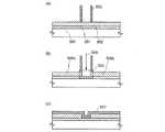
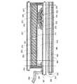
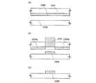
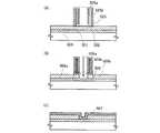
図1を用いて具体的に説明する。本実施の形態では、図1(A)に示すように、絶縁表面を有する基板500上に、導電層501を形成し、導電層501上に絶縁層502を形成する。絶縁層502の開口形成領域にチューブ503を絶縁層502に接して設ける。図1には、チューブ503を支持する手段を示していないが、チューブ503は絶縁層502に接触して保持されていればよい。例えば、チューブを基板上に設けて、基板を支持手段(支持基板)として用いたり、被処理膜上に支持手段として、支持膜を形成し、支持膜にチューブを挿入することでチューブを被処理膜上に保持してもよい。This will be specifically described with reference to FIG. In this embodiment, as illustrated in FIG. 1A, a
支持手段によって支持されたチューブは、移動制御手段によって、被処理膜上の所定の位置に被処理膜に接して設置される。まず、被処理膜の被加工面に対応する位置にチューブを移動する。次に被処理膜に接するようにチューブを移動させ、支持手段によって保持する。チューブを被処理膜に挿入する場合、チューブを被処理膜に挿入した状態で支持手段によって保持する。被処理膜の載置するステージを移動させ、チューブに接するようにしてもよい。The tube supported by the support means is placed in contact with the film to be processed at a predetermined position on the film to be processed by the movement control means. First, the tube is moved to a position corresponding to the processing surface of the film to be processed. Next, the tube is moved so as to be in contact with the film to be processed, and is held by the supporting means. When the tube is inserted into the film to be processed, the tube is held by the support means while being inserted into the film to be processed. The stage on which the film to be processed is placed may be moved so as to be in contact with the tube.
図40に支持膜520a、520bを用いてチューブ503を支持する例を示す。図40は図1に対応しており、支持膜520a、520bを形成する他は図1と同様である。図40において、絶縁層502に接して配置されるチューブ503は支持膜520a、520bによって支持されている。支持膜を形成した後、チューブを挿入して固定してもよいし、チューブを開口形成領域に設けた後、チューブ周囲を支持するように支持膜を形成してもよい。FIG. 40 shows an example in which the
エッチングガス509を吐出して絶縁層502に開口505を形成した後(図40(B)参照。)、支持膜520a、520bも除去する(図40(C)参照。)。絶縁層506a、506b、露出された導電層501上に導電膜507を形成し、開口505において導電層501と導電膜507とを電気的に接続する(図40(D)参照。)。After the
チューブ503を選択的に設けた状態でチューブ503を通してエッチングガス509を絶縁層502に噴出(吐出)する。噴出(吐出)されたエッチングガス509によって、絶縁層502を選択的に除去し、絶縁層502に開口505を形成する(図1(B)参照。)。An
チューブ503を除去し、開口505を有する絶縁層506a、506bを形成することができる。導電層501が露出された開口505に導電膜507を形成し、導電層501と導電膜507とを電気的に接続することができる(図1(C)参照。)。The
開口の形状はチューブの形状を反映するため、所望の形状が得られるようにチューブを設定すればよい。チューブは柱状(角柱、円柱、三角柱など)、針状などを用いることができる。また開口の深さ方向はチューブを設ける時の力と、チューブが設置される導電層の膜強度によって設定することができる。また、エッチング時間などのエッチング条件を設定することによっても膜厚方向の深さを選択できる。Since the shape of the opening reflects the shape of the tube, the tube may be set so as to obtain a desired shape. The tube may have a columnar shape (such as a prism, a cylinder, or a triangular column), a needle shape, or the like. The depth direction of the opening can be set by the force when the tube is provided and the film strength of the conductive layer where the tube is installed. The depth in the film thickness direction can also be selected by setting etching conditions such as etching time.
また、チューブの上面形状を、点状、円形、楕円形、矩形、または線状(厳密には細長い長方形状)と適宜設定すると、得られる絶縁層の開口の上面形状も同様にチューブ及びその吐出口形状を反映して形成することができる。In addition, when the top surface shape of the tube is appropriately set as a dotted, circular, elliptical, rectangular, or linear shape (strictly, a long and narrow rectangular shape), the top surface shape of the opening of the obtained insulating layer is similarly the tube and its discharge. It can be formed reflecting the shape of the outlet.
また、チューブは複数重なる構造でもよく、チューブが2重構造になっている例を図41に示す。本発明においてチューブは吐出を行うだけでなく、吸引もすることができる。図41は図1に対応しており、チューブ523のみが異なる例であり、他は図1と同様である。Further, a plurality of tubes may be stacked, and an example in which the tubes have a double structure is shown in FIG. In the present invention, the tube can perform not only discharge but also suction. FIG. 41 corresponds to FIG. 1, and is an example in which only the
図41(A)に示すチューブ523は、内側にチューブ525a、外側にチューブ525bを有している。チューブ525aはチューブ525bよりやや短く、絶縁層502との間に空間を有して配置される。図41(B)に示すようにチューブ523の内側のチューブ525a内を通ってエッチングガス526aが吐出され、絶縁層502を選択的に除去していく。同時に、外側のチューブ525bと内側のチューブ525aとの間を通って、エッチングガス及び絶縁層502のエッチングされた絶縁性材料526bが矢印の方向に吸引され開口より除去される。このようにチューブ内部を隔てて材料の供給と廃棄(除去)を同時に行ってもよい。エッチングによる残渣が開口よりすぐ除去されるので、絶縁層のエッチング効率(エッチング時間、エッチング速度)を向上させることができる。絶縁層506a、506b、露出された導電層501上に導電膜507を形成し、開口505において導電層501と導電膜507とを電気的に接続する(図41(C)参照。)。A
図2に示すように、チューブを絶縁層開口形成領域に配置する時に、チューブの先端を絶縁層に挿入し一部絶縁層に埋め込むようにしてもよい。絶縁表面を有する基板510上に、導電層511を形成し、導電層511上に絶縁層512を形成する。絶縁層512の開口形成領域にチューブ513を絶縁層512にチューブ513の先端が一部埋め込むようにして設ける(図2(A)参照。)。図2には、チューブ513を支持する手段を示していないが、チューブ513は絶縁層512に接触して保持されていればよい。例えば、チューブを基板上に設けて、基板を支持手段(支持基板)として用いたり、被処理膜上に支持手段として、支持膜を形成し、支持膜にチューブを挿入することでチューブを被処理膜上に保持してもよい。またチューブ513は絶縁層512に一部埋め込まれているため、絶縁層512も支えとして働く。As shown in FIG. 2, when the tube is disposed in the insulating layer opening formation region, the tip of the tube may be inserted into the insulating layer and partially embedded in the insulating layer. A
チューブ513を選択的に設けた状態でそのチューブ513を通してエッチングガス519を絶縁層512に噴出(吐出)する。噴出(吐出)されたエッチングガス519によって、絶縁層512を選択的に除去し、絶縁層512に開口515を形成する(図2(B)参照。)。With the
チューブ513を除去することによって、開口515を有する絶縁層516a、516bを形成することができる。開口515は、チューブの形状を反映するため、側面に段差を有する形状となる。導電層511が露出された開口515に導電膜517を形成し、導電層511と導電膜517とを電気的に接続することができる(図2(C)参照。)。By removing the
絶縁層を選択的に除去するため、チューブより吐出されるエッチング物質は、エッチングガスでもよいし、エッチング液でもよい。エッチングはエッチングガス、エッチング液、エッチング条件を適宜設定することによって、異方的、等方的にエッチングすることができる。液状のエッチング液を用いて、等方的にエッチングを行う例を図3に示す。In order to selectively remove the insulating layer, the etching substance discharged from the tube may be an etching gas or an etching solution. Etching can be performed anisotropically and isotropically by appropriately setting an etching gas, an etchant, and etching conditions. FIG. 3 shows an example of isotropic etching using a liquid etching solution.
図3(A)乃至(C)で用いるチューブは、先端が細い円錐形状の例であり、エッチング液のような液状材料を充填するのに適している。絶縁表面を有する基板530上に、導電層531を形成し、導電層531上に絶縁層532を形成する。絶縁層532の開口形成領域にチューブ533を絶縁層532に接して配置する(図3(A)参照。)。チューブ533内部にはエッチング液539が充填されている。The tubes used in FIGS. 3A to 3C are examples having a conical shape with a thin tip, and are suitable for filling a liquid material such as an etching solution. A
チューブ533を選択的に設けた状態でそのチューブ533を通してエッチング液539を絶縁層532に吐出する。吐出されたエッチング液539によって、絶縁層532を選択的に除去し、絶縁層532に開口535を形成する(図3(B)参照。)。With the
次にチューブ533を除去することによって、開口535を有する絶縁層536a、536bを形成することができる。開口535は、エッチング液539により等方的にエッチングされるため、図3(B)に示すようにチューブ533の吐出口より広い領域に開口が形成される。導電層531が露出された開口535に導電膜537を形成し、導電層531と導電膜537とを電気的に接続することができる(図3(C)参照。)。Next, by removing the
エッチング液によって絶縁層は溶解されるが、エッチング液と絶縁層形成材料の混在した溶液をチューブを通して吸引し、除去してもよい。本発明の中空構造を有し先端が開口している細管であるチューブは吐出を行うだけでなく、吸引もすることができる。Although the insulating layer is dissolved by the etching solution, a solution in which the etching solution and the insulating layer forming material are mixed may be sucked through the tube and removed. The tube, which is a thin tube having a hollow structure according to the present invention and having an open end, can not only discharge but also suction.
本発明において、エッチング液のような液状の材料をチューブを通して被処理膜を加工する場合、液状の材料(例えばエッチング液)に対して、撥液処理するとよい。撥液処理は、被処理膜上に撥液性を有する物質を含む膜を形成することによって行うことができる。被処理膜表面で液状の材料(エッチング液など)ははじかれるので、液状の材料(エッチング液など)が被処理膜とチューブとの間より流出しにくくすることができる。従って、被処理膜表面の凹凸などによってチューブを密着して配置できなかった場合でも、エッチング液などがチューブ外に流出(吐出)して被処理膜の処理領域外の領域を加工してしまうという不良を防ぐことができる。制御性よく被処理膜に所望の形状に開口を形成することができる。In the present invention, when a film to be processed is processed through a tube with a liquid material such as an etching solution, a liquid repellent treatment may be performed on the liquid material (for example, an etching solution). The liquid repellent treatment can be performed by forming a film containing a liquid repellent substance on the film to be processed. Since a liquid material (such as an etchant) is repelled on the surface of the film to be processed, the liquid material (such as an etchant) can be more unlikely to flow out between the film to be processed and the tube. Therefore, even when the tube cannot be placed in close contact due to the unevenness of the surface of the film to be processed, the etching solution or the like flows out (discharges) out of the tube, and the region outside the processing region of the film to be processed is processed. Defects can be prevented. An opening can be formed in a desired shape in the film to be processed with good controllability.
撥液性を有する物質として、フッ化炭素基(フッ化炭素鎖)を含む物質、あるいはシランカップリング剤を含む物質を用いることができる。シランカップリング剤は単分子膜を形成することができるため、分解、改質を効率よく行え、短時間でぬれ性を変化させることができる。また、シランカップリング剤は、フッ化炭素基(フッ化炭素鎖)を有するもののみでなく、アルキル基を有するものも基板に配列させることで、低ぬれ性を示すため、用いることが可能である。またシランカップリング剤は含まれる官能基がフッ化炭素基かアルキル基によって、そのぬれ性を低める効果が異なるので、必要なぬれ性が得られるように材料によって適宜設定することができる。As the substance having liquid repellency, a substance containing a fluorocarbon group (fluorocarbon chain) or a substance containing a silane coupling agent can be used. Since the silane coupling agent can form a monomolecular film, it can be efficiently decomposed and modified, and the wettability can be changed in a short time. Silane coupling agents can be used because they exhibit low wettability by arranging not only those having a fluorocarbon group (fluorocarbon chain) but also those having an alkyl group on the substrate. is there. Moreover, since the functional group contained in the silane coupling agent differs depending on the fluorocarbon group or the alkyl group in reducing the wettability, it can be appropriately set depending on the material so as to obtain the required wettability.
撥液性を有する物質として、フッ化炭素基(フッ化炭素鎖)を含む物質、あるいはシランカップリング剤を含む物質を用いることができる。シランカップリング剤は、Rn−Si−X(4−n)(n=1、2、3)の化学式で表される。ここで、Rは、アルキル基などの比較的不活性な基を含む物である。また、Xはハロゲン、メトキシ基、エトキシ基又はアセトキシ基など、基質表面の水酸基あるいは吸着水との縮合により結合可能な加水分解基からなる。As the substance having liquid repellency, a substance containing a fluorocarbon group (fluorocarbon chain) or a substance containing a silane coupling agent can be used. The silane coupling agent is represented by a chemical formula of Rn—Si—X(4-n) (n = 1, 2, 3). Here, R is a substance containing a relatively inert group such as an alkyl group. X is a hydrolyzable group such as halogen, methoxy group, ethoxy group or acetoxy group, which can be bonded by condensation with a hydroxyl group on the substrate surface or adsorbed water.
撥液性を有する物質として、シランカップリング剤のRに、アルキル基を有す物質であるアルコキシシランも用いることができ、例えば有機シランとしてオクタデシルトリメトキシシラン等を用いることができる。アルコキシシランとしては、炭素数2〜30のアルコキシシランが好ましい。代表的には、デシルトリメトキシシラン、エチルトリエトキシシラン、プロピルトリエトキシシラン、オクチルトリエトキシシラン、デシルトリエトキシシラン、ドデシルトリエトキシシラン、オクタデシルトリエトキシシラン(ODS)、エイコシルトリエトキシシラン、トリアコンチルトリエトキシシランがあげられる。なお、長鎖アルキル基を有するシラン化合物は、特にぬれ性を低下させることが可能であり好ましい。また、デシルトリクロロシラン、テトラデシルトリクロロシラン、オクタデシルトリクロロシラン、エイコシルトリクロロシラン、ドコシルトリクロロシラン等も用いることができる。As a substance having liquid repellency, alkoxysilane which is a substance having an alkyl group can be used for R of the silane coupling agent. For example, octadecyltrimethoxysilane or the like can be used as an organic silane. As alkoxysilane, C2-C30 alkoxysilane is preferable. Typically, decyltrimethoxysilane, ethyltriethoxysilane, propyltriethoxysilane, octyltriethoxysilane, decyltriethoxysilane, dodecyltriethoxysilane, octadecyltriethoxysilane (ODS), eicosyltriethoxysilane, tria An example is contitriethoxysilane. A silane compound having a long-chain alkyl group is particularly preferable because it can reduce wettability. Further, decyltrichlorosilane, tetradecyltrichlorosilane, octadecyltrichlorosilane, eicosyltrichlorosilane, docosyltrichlorosilane, and the like can also be used.
また、シランカップリング剤の代表例として、Rにフルオロアルキル基を有するフッ素系シランカップリング剤(フルオロアルキルシラン(FAS))を用いることにより、よりぬれ性を低めることができる。FASのRは、(CF3)(CF2)x(CH2)y(x:0以上10以下の整数、y:0以上4以下の整数)で表される構造を持ち、複数個のR又はXがSiに結合している場合には、R又はXはそれぞれすべて同じでも良いし、異なっていてもよい。代表的なFASとしては、ヘプタデカフルオロテトラヒドロデシルトリエトキシシラン、ヘプタデカフルオロテトラヒドロデシルトリクロロシラン、トリデカフルオロテトラヒドロオクチルトリクロロシラン、トリフルオロプロピルトリメトキシシラン、トリデカフルオロオクチルトリメトキシシラン等のフルオロアルキルシラン(以下、FASともいう。)が挙げられる。また、トリデカフルオロオクチルトリクロロシラン等の加水分解基がハロゲンであるカップリング剤も用いることができる。もちろん例示の化合物に限定される物ではない。Further, as a representative example of the silane coupling agent, wettability can be further reduced by using a fluorine-based silane coupling agent (fluoroalkylsilane (FAS)) having a fluoroalkyl group in R. R of FAS has a structure represented by (CF3 ) (CF2 )x (CH2 )y (x: an integer of 0 or more and 10 or less, y: an integer of 0 or more and 4 or less), and a plurality of R Alternatively, when X is bonded to Si, R and X may all be the same or different. As typical FAS, fluoroalkyl such as heptadecafluorotetrahydrodecyltriethoxysilane, heptadecafluorotetrahydrodecyltrichlorosilane, tridecafluorotetrahydrooctyltrichlorosilane, trifluoropropyltrimethoxysilane, tridecafluorooctyltrimethoxysilane, etc. Silane (hereinafter also referred to as FAS) can be given. In addition, a coupling agent such as tridecafluorooctyltrichlorosilane whose hydrolyzable group is halogen can also be used. Of course, the compounds are not limited to the exemplified compounds.
また、撥液性を有する物質としてチタネートカップリング剤、アルミネートカップリング剤を用いてもよい。例えば、イソプロピルトリイソオクタノイルチタネート、イソプロピル(ジオクチルパイロホスフェート)チタネート、イソプロピルトリステアロイルチタネート、イソプロピルトリス(ジオクチルホスフェート)チタネート、イソプロピルジメタクリルイソステアロイルチタネート、アセトアルコキシアルミニウムジイソプロピレート等が挙げられる。Further, a titanate coupling agent or an aluminate coupling agent may be used as the substance having liquid repellency. For example, isopropyl triisooctanoyl titanate, isopropyl (dioctyl pyrophosphate) titanate, isopropyl tristearoyl titanate, isopropyl tris (dioctyl phosphate) titanate, isopropyl dimethacrylisostearoyl titanate, acetoalkoxy aluminum diisopropylate and the like can be mentioned.
上記のような撥液性を有する物質を被形成領域に膜として形成するには、液状の物質を蒸発させ、被形成領域に形成する気相成膜法などを用いることができる。また、撥液性を有する物質はスピンコート法、ディップ法、液滴吐出法、印刷法(スクリーン印刷やオフセット印刷など)を用いて形成することもでき、溶媒に溶解した溶液としてもよい。In order to form the liquid repellent material as a film in the formation region, a vapor deposition method in which a liquid substance is evaporated and formed in the formation region can be used. The substance having liquid repellency can be formed by a spin coating method, a dip method, a droplet discharge method, a printing method (such as screen printing or offset printing), or a solution in a solvent.
撥液性を有する物質を含む溶液の溶媒としては、水、アルコール、ケトン、炭化水素系溶媒(脂肪族炭化水素、芳香族炭化水素、ハロゲン化炭化水素など)、及びエーテル系化合物、及びこれらの混合物を用いることができる。例えば、メタノール、エタノール、プロパノール、アセトン、ブタノン、n−ペンタン、n−ヘキサン、n−ヘプタン、n−オクタン、n−デカン、ジシクロペンタン、ベンゼン、トルエン、キシレン、デュレン、インデン、テトラヒドロナフタレン、デカヒドロナフタレン、スクワラン、四塩化炭素、クロロホルム、塩化メチレン、トリクロロエタン、ジエチルエーテル、ジオキサン、ジメトキシエタン又はテトラヒドロフランなどを用いる。上記溶液の濃度は特に限定はないが、0.001〜20wt%の範囲とすればよい。As a solvent of a solution containing a substance having liquid repellency, water, alcohol, ketone, hydrocarbon solvent (aliphatic hydrocarbon, aromatic hydrocarbon, halogenated hydrocarbon, etc.), ether compound, and these Mixtures can be used. For example, methanol, ethanol, propanol, acetone, butanone, n-pentane, n-hexane, n-heptane, n-octane, n-decane, dicyclopentane, benzene, toluene, xylene, durene, indene, tetrahydronaphthalene, deca Hydronaphthalene, squalane, carbon tetrachloride, chloroform, methylene chloride, trichloroethane, diethyl ether, dioxane, dimethoxyethane, tetrahydrofuran, or the like is used. The concentration of the solution is not particularly limited, but may be in the range of 0.001 to 20 wt%.
また、上記撥液性を有する物質に、ピリジン、トリエチルアミン、ジメチルアニリン等のアミンを混合してもよい。更に、ギ酸、酢酸等のカルボン酸を触媒として添加してもよい。Further, amines such as pyridine, triethylamine, dimethylaniline may be mixed with the liquid repellent material. Further, a carboxylic acid such as formic acid or acetic acid may be added as a catalyst.
上記のように撥液性を有する物質を液状の状態で被形成領域に付着させるスピンコート法等を用いて単分子膜を形成する際の処理は、処理温度は室温(約25℃)から150℃、処理時間は数分から12時間とすればよい。処理条件は、撥液性を有する物質の性質、溶液の濃度、処理温度、処理時間によって適宜設定すればよい。また、形成する薄膜を上記撥液性を有する物質を含む溶液を作成する際に用いることのできる溶媒で洗浄すると、未反応の撥液性を有する物質を除去することができる。この場合、超音波洗浄器等を用いてもよい。As described above, the processing temperature when forming a monomolecular film using a spin coat method or the like in which a liquid-repellent substance is attached to a formation region in a liquid state is from room temperature (about 25 ° C.) to 150 ° C. The treatment time may be from several minutes to 12 hours. The treatment conditions may be appropriately set depending on the properties of the substance having liquid repellency, the concentration of the solution, the treatment temperature, and the treatment time. In addition, when the thin film to be formed is washed with a solvent that can be used for preparing a solution containing the liquid repellent substance, the unreacted liquid repellent substance can be removed. In this case, an ultrasonic cleaner or the like may be used.
本発明で用いることのできる撥液性を有する物質を含む膜は膜厚0.3nm以上10nm以下という薄膜でもよい。なお、撥液性を有する物質を液状の状態で被形成領域に付着させるスピンコート法等を用いて形成する撥液性を有する物質の薄膜は非常に薄く、膜厚が0.3nm以上10nm以下の範囲の単分子膜となり得る。The film containing a liquid-repellent substance that can be used in the present invention may be a thin film with a thickness of 0.3 nm to 10 nm. Note that a thin film of a material having liquid repellency formed using a spin coating method or the like in which a substance having liquid repellency is attached to a formation region in a liquid state is very thin and has a thickness of 0.3 nm to 10 nm. It can be a monomolecular film in the range.
また、ぬれ性を低めるように制御し、低ぬれ性領域を形成する組成物の一例として、フッ化炭素(フルオロカーボン)基(フッ化炭素鎖)を有する材料(フッ素系樹脂)を用いることができる。フッ素系樹脂として、ポリテトラフルオロエチレン(PTFE;四フッ化エチレン樹脂)、パーフルオロアルコキシアルカン(PFA;四フッ化エチレンパーフルオロアルキルビニルエーテル共重合樹脂)、パーフルオロエチレンプロペンコーポリマー(PFEP;四フッ化エチレン−六フッ化プロピレン共重合樹脂)、エチレン−テトラフルオロエチレンコポリマー(ETFE;四フッ化エチレン−エチレン共重合樹脂)、ポリビニリデンフルオライド(PVDF;フッ化ビニリデン樹脂)、ポリクロロトリフルオロエチレン(PCTFE;三フッ化塩化エチレン樹脂)、エチレン−クロロトリフルオロエチレンコポリマー(ECTFE;三フッ化塩化エチレン−エチレン共重合樹脂)、ポリテトラフルオロエチレン−パーフルオロジオキソールコポリマー(TFE/PDD)、ポリビニルフルオライド(PVF;フッ化ビニル樹脂)等を用いることができる。In addition, as an example of a composition that is controlled to reduce wettability and forms a low wettability region, a material having a fluorocarbon (fluorocarbon) group (fluorocarbon chain) (fluorine-based resin) can be used. . Examples of fluorine resins include polytetrafluoroethylene (PTFE; tetrafluoroethylene resin), perfluoroalkoxyalkane (PFA; tetrafluoroethylene perfluoroalkyl vinyl ether copolymer resin), and perfluoroethylene propene copolymer (PFEP; four fluoropolymer). Ethylene-hexafluoropropylene copolymer resin), ethylene-tetrafluoroethylene copolymer (ETFE; tetrafluoroethylene-ethylene copolymer resin), polyvinylidene fluoride (PVDF; vinylidene fluoride resin), polychlorotrifluoroethylene (PCTFE; trifluoroethylene chloride resin), ethylene-chlorotrifluoroethylene copolymer (ECTFE; trifluoroethylene chloride-ethylene copolymer resin), polytetrafluoroethylene-perfluorodioxide Rukoporima (TFE / PDD), polyvinyl fluoride (PVF; a vinyl fluoride resin), or the like can be used.
また、無機材料、有機材料にCF4プラズマ等による処理を行うと、ぬれ性を低めることができる。例えば、有機材料としてポリビニルアルコール(PVA)のような水溶性樹脂を、H2O等の溶媒に混合した材料を用いることができる。また、PVAと他の水溶性樹脂を組み合わせて使用してもよい。In addition, when an inorganic material or an organic material is treated with CF4 plasma or the like, wettability can be reduced. For example, a material obtained by mixing a water-soluble resin such as polyvinyl alcohol (PVA) in a solvent such as H2 O as an organic material can be used. Moreover, you may use combining PVA and another water-soluble resin.
エッチングスとしては、Cl2、BCl3、SiCl4もしくはCCl4などを代表とする塩素系ガス、CF4、SF6もしくはNF3などを代表とするフッ素系ガス又はO2を適宜用いることができる。エッチング液としては、フッ酸、水酸化テトラメチルアンモニウム水溶液(TMAH)などを適宜用いるとよい。Etchings may be appropriately used a chlorine-based gas typified by Cl2 , BCl3 , SiCl4 or CCl4 , a fluorine-based gas typified by CF4 , SF6 or NF3, or O2. . As an etchant, hydrofluoric acid, tetramethylammonium hydroxide aqueous solution (TMAH), or the like may be used as appropriate.
本発明のチューブは、内部に空間を有し、材料を吐出、吸引できるものである。吐出はピエゾ素子のような素子により行うことができ、吸引はポンプ等で行えばよい。従ってチューブに接続して、材料を供給する供給手段と材料貯蔵室、吸収した材料を廃棄するまで保管する貯蔵庫を有してもよい。The tube of the present invention has a space inside and can discharge and suck materials. The ejection can be performed by an element such as a piezo element, and the suction can be performed by a pump or the like. Therefore, it may have a supply means for supplying the material, a material storage chamber, and a storage for storing the absorbed material until it is discarded, connected to the tube.
さらに、本発明のチューブによって絶縁層に開口を形成した後、チューブ内部を通して液状の膜形成材料(例えば導電性を有する組成物)を開口に吐出し、導電層を形成してもよい。Furthermore, after forming an opening in the insulating layer by the tube of the present invention, a liquid film forming material (for example, a conductive composition) may be discharged into the opening through the tube to form the conductive layer.
開口が微細であると、液状の膜形成材料は表面張力の関係より開口に確実に充填されにくい場合があるが、本発明であると、開口に挿入されたチューブによって確実に開口に膜形成材料を充填でき、形状不良なく膜を形成することができる。If the opening is fine, the liquid film-forming material may not be reliably filled into the opening due to the surface tension. However, in the present invention, the film-forming material is reliably attached to the opening by the tube inserted into the opening. The film can be formed without a shape defect.
チューブより吐出されるエッチングガスは、チューブが耐えられるものであればエッチングする薄膜によって適宜選択することができる。例えば、幾層にも積層する多層配線などを作製する場合、何層にもわたって異なる薄膜に連続的な開口を形成する際に本発明を用いることができる。The etching gas discharged from the tube can be appropriately selected depending on the thin film to be etched as long as the tube can withstand. For example, in the case of producing a multilayer wiring or the like laminated in several layers, the present invention can be used in forming continuous openings in different thin films over several layers.
また開口の深さ方向はチューブを設ける時の力と、チューブが設置される膜の膜強度によって設定することができる。先端の尖った針のようなチューブを用いると、膜に挿入する時の抵抗を低くすることができる。The depth direction of the opening can be set by the force when the tube is provided and the film strength of the film on which the tube is installed. When a tube such as a needle with a sharp tip is used, the resistance when inserted into the membrane can be lowered.
導電層501、511、531、導電膜507、517、537は蒸着法、スパッタリング法、PVD法(Physical Vapor Deposition)、減圧CVD法(LPCVD法)、またはプラズマCVD法等のCVD法(Chemical Vapor Deposition)などを用いて形成することができる。また、構成物が所望のパターンに転写、または描写できる方法、例えば各種印刷法(スクリーン(孔版)印刷、オフセット(平版)印刷、凸版印刷やグラビア(凹版)印刷など所望なパターンで形成される方法)、ディスペンサ法、選択的な塗布法なども用いることができる。The
導電層501、511、531、導電膜507、517、537として、Ag、Au、Ni、Pt、Pd、Ir、Rh、Ta、W、Ti、Mo、Al、Cu、Cr、Coから選ばれたうち一種又は複数の元素、又は前記元素を主成分とする合金材料もしくは化合物材料で形成すればよい。また、リン等の不純物元素をドーピングした多結晶シリコン膜に代表される半導体膜や、AgPdCu合金を用いてもよい。また、単層構造でも複数層の構造でもよく、例えば、窒化タングステン膜とモリブデン(Mo)膜との2層構造としてもよいし、膜厚50nmのタングステン膜、膜厚500nmのアルミニウムとシリコンの合金(Al−Si)膜、膜厚30nmの窒化チタン膜を順次積層した3層構造としてもよい。また、3層構造とする場合、第1の導電膜のタングステンに代えて窒化タングステンを用いてもよいし、第2の導電膜のアルミニウムとシリコンの合金(Al−Si)膜に代えてアルミニウムとチタンの合金膜(Al−Ti)を用いてもよいし、第3の導電膜の窒化チタン膜に代えてチタン膜を用いてもよい。The
導電層501、511、531、導電膜507、517、537としてまた、インジウム錫酸化物(ITO)、酸化珪素を含むインジウム錫酸化物(ITSO)、酸化亜鉛(ZnO)、酸化亜鉛にガリウム(Ga)をドープした導電性材料、インジウム亜鉛酸化物(IZO(indium zinc oxide))を用いても良い。また、導電層の代わりに半導体層を形成する場合は、半導体材料を用いればよく、例えば、シリコン(珪素)、ゲルマニウム、シリコンゲルマニウム、ガリウム砒素、酸化モリブデン、酸化スズ、酸化ビスマス、酸化バナジウム、酸化ニッケル、酸化亜鉛、ヒ化ガリウム、窒化ガリウム、酸化インジウム、リン化インジウム、窒化インジウム、硫化カドミウム、テルル化カドミウム、チタン酸ストロンチウムなどの無機半導体材料を用いることができる。As the
絶縁層502、512、532は、スパッタリング法、PVD法(Physical Vapor Deposition)、減圧CVD法(LPCVD法)、またはプラズマCVD法等のCVD法(Chemical Vapor Deposition)などにより形成することができる。また、液滴吐出法や、印刷法(スクリーン印刷やオフセット印刷などパターンが形成される方法)、スピンコート法などの塗布法、ディッピング法、ディスペンサ法などを用いることもできる。The insulating
絶縁層502、512、532は、酸化珪素、窒化珪素、酸化窒化珪素、酸化アルミニウム、窒化アルミニウム、酸化窒化アルミニウム、ダイアモンドライクカーボン(DLC)、窒素含有炭素(CN)、ポリシラザン、その他の無機絶縁性材料を含む物質から選ばれた材料で形成することができる。また、シロキサンを含む材料を用いてもよい。また、有機絶縁性材料を用いてもよく、有機材料としては、ポリイミド、アクリル、ポリアミド、ポリイミドアミド、レジスト又はベンゾシクロブテンを用いることができる。また、オキサゾール樹脂を用いることもできる。The insulating
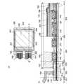
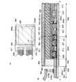
本発明を用いて半導体装置や表示装置を作製することができるが、図42に本発明のエッチング装置の例を示す。Although a semiconductor device and a display device can be manufactured using the present invention, FIG. 42 shows an example of an etching apparatus of the present invention.
図42に示すように、エッチング装置330は、チューブ301、位置制御手段302、吐出制御手段303、吐出材料貯蔵室304、吸引制御手段305、吸引材料貯蔵室306、コック307、コック308を有している。エッチング装置330は、成膜装置として機能することができる。チューブ301は位置制御手段302によって移動することができ、被処理膜に接するように配置される。吐出材料貯蔵室304とチューブ301とはコック307を介して接続されており、材料吐出時はコック307が開放され、吐出制御手段303によってチューブ301より材料が吐出される。一方、吸引材料貯蔵室306とチューブ301とはコック308を介して接続されており、材料吸引時はコック308が開放され、吸引制御手段305によってチューブ301より吐出した材料などが吸引され、吸引材料貯蔵室306へと送られる。吸引材料貯蔵室306に貯蔵された材料は廃棄、また再び吐出材料貯蔵室へ送られて再利用することができる。吐出制御手段303としてはピエゾ素子などを用いることができ、吸引制御手段305にはポンプなどを用いることができる。吐出、吸引の制御を的確に行うために真空計などを設けるとよい。As shown in FIG. 42, the etching apparatus 330 includes a tube 301, a position control unit 302, a discharge control unit 303, a discharge material storage chamber 304, a suction control unit 305, a suction material storage chamber 306, a cock 307, and a cock 308. ing. The etching apparatus 330 can function as a film formation apparatus. The tube 301 can be moved by the position control means 302 and is arranged so as to contact the film to be processed. The discharge material storage chamber 304 and the tube 301 are connected via a cock 307, the cock 307 is opened during material discharge, and the material is discharged from the tube 301 by the discharge control means 303. On the other hand, the suction material storage chamber 306 and the tube 301 are connected via a cock 308. When sucking the material, the cock 308 is opened, and the material discharged from the tube 301 is sucked by the suction control means 305. It is sent to the storage room 306. The material stored in the suction material storage chamber 306 can be discarded or sent again to the discharge material storage chamber for reuse. A piezo element or the like can be used as the discharge control means 303, and a pump or the like can be used as the suction control means 305. A vacuum gauge or the like may be provided in order to accurately control discharge and suction.
図42ではチューブによる吸引手段と吐出手段を備えた例を示したが、本発明はこれに限定されず、チューブによる吐出手段のみを備えてもよいし、チューブからの吐出、吸引を減圧下で行えるように減圧手段を設けてもよい。FIG. 42 shows an example in which a suction means and a discharge means using a tube are provided. However, the present invention is not limited to this, and only a discharge means using a tube may be provided, and discharge and suction from the tube may be performed under reduced pressure. A pressure reducing means may be provided so that it can be performed.
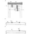
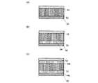
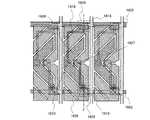
絶縁層に複数の開口を形成する場合、支持基板に複数のチューブを有するようなチューブ群を用いることができる。複数の開口を形成することのできるチューブ部の例を、図34を用いて説明する。In the case where a plurality of openings are formed in the insulating layer, a tube group having a plurality of tubes on the support substrate can be used. An example of a tube portion that can form a plurality of openings will be described with reference to FIG.
図34(A)はチューブ部を支持基板側より見た平面図であり、図34(B)(C)は図34(A)において線O−Pの断面図である。34A is a plan view of the tube portion viewed from the support substrate side, and FIGS. 34B and 34C are cross-sectional views taken along line OP in FIG. 34A.
図34(A)において、チューブ部353は支持基板350、チューブ351を有している。支持手段である支持基板350上に、開口形成領域と対応している場所に複数のチューブ351が設けられている。移動制御手段により移動可能な支持手段により、支持基板をチューブ351が被処理膜に接触するように移動し、被処理膜に対向してチューブ部353を設ければよい。移動制御手段により支持手段及びチューブは移動可能であり、チューブを被処理膜において膜厚方向上下、基板方向に上下左右に移動させ、被処理膜に対するチューブの位置を制御する。In FIG. 34A, the
チューブは、回路設計図面データから、絶縁層において所望の位置に開口を形成できるように設定すればよい。また、開口形成手段と被処理膜の形成される基板との位置関係は、予めチューブ部を支持する支持基板及び被処理膜の形成される基板にマーカを形成しておき位置合わせを行えばよい。The tube may be set so that an opening can be formed at a desired position in the insulating layer from the circuit design drawing data. Further, the positional relationship between the opening forming means and the substrate on which the film to be processed is formed may be adjusted by previously forming a marker on the support substrate that supports the tube portion and the substrate on which the film to be processed is formed. .
図34(B)において、チューブ351には制御素子354が設けられており、チューブ351の上下位置の移動を制御することができる。制御素子354としてはピエゾ素子などを用いることができる。図34(C)は制御素子によって選択的にチューブの位置が制御された例である。図34(C)において制御素子355aによりチューブ356aが移動し、チューブ356aの先端は選択されていない制御素子355bのチューブ356bの先端より距離d下に位置する。このように開口を形成する領域のみにチューブを選択的に基板上の被処理膜に配置して、所望の場所に開口を形成することができる。In FIG. 34B, a
絶縁層に開口を形成後、チューブの除去はチューブを物理的に引き抜く等して除去してもよいし、開口を有する絶縁層とエッチングの選択比が高い条件で、チューブをエッチング(ドライエッチング又はウエットエッチング)によって化学的に除去してもよい。絶縁層と導電層との密着強度が弱い場合は、エッチングによってチューブを除去するのが好ましい。また、チューブを形状変化することなく絶縁層より物理的手段により除去すると、除去作業が容易でありチューブを繰り返し再利用することができるため、コストを削減することができるという利点がある。After forming the opening in the insulating layer, the tube may be removed by physically pulling out the tube, or the tube is etched (dry etching or dry etching) under a condition where the etching ratio between the insulating layer having the opening and the etching is high. It may be chemically removed by wet etching. When the adhesion strength between the insulating layer and the conductive layer is weak, it is preferable to remove the tube by etching. Further, when the tube is removed from the insulating layer by physical means without changing its shape, there is an advantage that the removal work is easy and the tube can be reused repeatedly, thereby reducing the cost.
チューブはスパッタリング法、真空蒸着法、PVD法(Physical Vapor Deposition)、減圧CVD法(LPCVD法)、またはプラズマCVD法等のCVD法(Chemical Vapor Deposition)により薄膜を成膜した後、所望の形状にエッチングして形成することができる。また、選択的にパターンを形成できる液滴吐出法や、パターンが転写または描写できる印刷法(スクリーン印刷やオフセット印刷などパターンが形成される方法)、その他スピンコート法などの塗布法、ディッピング法、ディスペンサ法などを用いることもできる。また、インプリント技術、ナノメートルサイズの立体構造物を転写技術で形成できるナノインプリント技術を用いることもができる。インプリント、ナノインプリントは、フォトリソグラフィー工程を用いずに微細な立体構造物を形成できる技術である。The tube is formed into a desired shape after a thin film is formed by a sputtering method, a vacuum deposition method, a PVD method (Physical Vapor Deposition), a low pressure CVD method (LPCVD method), or a CVD method (Chemical Vapor Deposition) such as a plasma CVD method. It can be formed by etching. In addition, a droplet discharge method that can selectively form a pattern, a printing method that can transfer or depict a pattern (a method that forms a pattern such as screen printing or offset printing), other coating methods such as spin coating, dipping method, A dispenser method or the like can also be used. In addition, an imprint technique and a nanoimprint technique that can form a nanometer-sized three-dimensional structure by a transfer technique can also be used. Imprinting and nanoimprinting are techniques that can form fine three-dimensional structures without using a photolithography process.
無機材料でも有機材料又は珪素と酸素との結合で骨格構造が形成された材料で形成してもよい。絶縁膜の成膜を遮蔽する手段であるので、金属などの導電材料でも、樹脂などの絶縁材料でもよい。また、繊維などを用いることもできる。装置に設置することを考慮すると、比較的軽量で加工の容易なものが好ましい。微細な開口を形成する場合は、カーボンナノチューブなどの、ナノチューブ材料を用いることもできる。カーボンナノチューブなどの極細炭素繊維は、グラファイトナノファイバ、カーボンナノファイバ、チューブ状グラファイト、カーボンナノコーン、又はコーン状グラファイトなども用いることができる。An inorganic material or an organic material or a material in which a skeleton structure is formed by a bond of silicon and oxygen may be used. Since it is a means for shielding the formation of the insulating film, it may be a conductive material such as metal or an insulating material such as resin. Moreover, a fiber etc. can also be used. Considering the installation in the apparatus, a relatively light weight and easy processing is preferable. In the case of forming a fine opening, a nanotube material such as a carbon nanotube can be used. As the ultrafine carbon fiber such as carbon nanotube, graphite nanofiber, carbon nanofiber, tube-like graphite, carbon nanocone, cone-like graphite, or the like can also be used.
チューブの材料としては、酸化珪素、窒化珪素、酸化窒化珪素、酸化アルミニウム、窒化アルミニウム、酸化窒化アルミニウム、ダイアモンドライクカーボン(DLC)、窒素含有炭素(CN)、ポリシラザン、その他の無機絶縁性材料を含む物質から選ばれた材料で形成することができる。また、シロキサンを含む材料を用いてもよい。また、エポキシ樹脂、フェノール樹脂、ノボラック樹脂、アクリル樹脂、メラミン樹脂、ウレタン樹脂、ベンゾシクロブテン、パリレン、フッ化アリーレンエーテル、ポリイミドなどの有機材料、シロキサン結合を有する樹脂などを用いることができる。Tube materials include silicon oxide, silicon nitride, silicon oxynitride, aluminum oxide, aluminum nitride, aluminum oxynitride, diamond-like carbon (DLC), nitrogen-containing carbon (CN), polysilazane, and other inorganic insulating materials. It can be formed of a material selected from substances. Further, a material containing siloxane may be used. Alternatively, an epoxy resin, a phenol resin, a novolac resin, an acrylic resin, a melamine resin, a urethane resin, benzocyclobutene, parylene, fluorinated arylene ether, a polyimide resin, a resin having a siloxane bond, or the like can be used.
開口を形成した後、液体で開口付近に残存する導電性材料や絶縁性材料(導電層又は絶縁層の除去された部分の残存物)を洗浄し、残存物を除去してもよい。この場合、洗浄に水などの無反応物質を用いてもよいし、絶縁層と反応する(溶解する)エッチング液などの薬液を用いてもよい。エッチング液を用いると開口がオーバーエッチングされ、ゴミ等が除去され表面がより平坦化される。また開口を広げることもできる。After the opening is formed, the conductive material or insulating material remaining in the vicinity of the opening with a liquid (residue of the removed portion of the conductive layer or the insulating layer) may be washed to remove the residue. In this case, an unreacted substance such as water may be used for cleaning, or a chemical solution such as an etching solution that reacts (dissolves) with the insulating layer may be used. When an etching solution is used, the opening is over-etched, dust and the like are removed, and the surface is flattened. The opening can also be widened.
このように複雑なフォトリソグラフィ工程、レジストマスク層の形成を行うことなく、導電層と導電層(導電膜)とを電気的に接続する開口(コンタクトホール)を絶縁層に形成することができる。Thus, an opening (contact hole) for electrically connecting the conductive layer and the conductive layer (conductive film) can be formed in the insulating layer without performing a complicated photolithography process and formation of a resist mask layer.
従って、本実施の形態によれば、絶縁層にマスクを形成することなくコンタクトホールを形成することができるので、工程を簡略化することができる。また、フォトレジスト等を塗布して露光及び現像する必要がないので、加工に必要な原材料コストを削減することができる。さらに、コンタクトホールを確実に形成することができるので、製造歩留まりの向上を図ることができる。Therefore, according to this embodiment mode, a contact hole can be formed without forming a mask in the insulating layer, so that the process can be simplified. In addition, since it is not necessary to apply a photoresist or the like for exposure and development, it is possible to reduce raw material costs required for processing. Furthermore, since the contact hole can be reliably formed, the manufacturing yield can be improved.
(実施の形態2)
本実施の形態では、確実により簡略化した工程で低コストに作製することを目的とした積層構造のコンタクトホールを形成する方法について説明する。詳しくは実施の形態1において、コンタクトホールが複数の積層する膜に亘って形成される例である。従って、同一部分又は同様な機能を有する部分は実施の形態1と同様な材料及び方法を用いればよく、その繰り返しの説明は省略する。(Embodiment 2)
In this embodiment mode, a method for forming a contact hole having a stacked structure for the purpose of manufacturing at a low cost through a process that is surely simplified will be described. Specifically, in Embodiment 1, the contact hole is formed over a plurality of stacked films. Accordingly, the same portion or a portion having a similar function may be formed using the same material and method as those in Embodiment Mode 1, and the description thereof is not repeated.
チューブを絶縁層に挿入し、一部埋め込むように配置し、物理的力によって絶縁層に第1の開口を形成し、その後、吐出口からエッチングガスを噴出してさらに絶縁層を選択的に除去し、第2の開口を形成することができる。つまりチューブの物理的な力で第1の開口を形成し、チューブより吐出される処理剤(エッチングガス又はエッチング液)の化学的な力によって第2の開口を形成してもよい。先にチューブより処理剤(エッチングガス又はエッチング液)を吐出して、第1の開口を形成し、チューブを絶縁層に挿入して第2の開口を形成してもよいし、エッチングガスを吐出しながら同時にチューブを絶縁層に挿入して開口を形成してもよい。Insert the tube into the insulating layer and place it so as to embed part of it, form a first opening in the insulating layer by physical force, and then eject the etching gas from the discharge port to further remove the insulating layer selectively Then, the second opening can be formed. That is, the first opening may be formed by a physical force of the tube, and the second opening may be formed by a chemical force of a processing agent (etching gas or etching solution) discharged from the tube. First, the processing agent (etching gas or etching solution) is discharged from the tube to form the first opening, and the tube may be inserted into the insulating layer to form the second opening, or the etching gas is discharged. At the same time, the tube may be inserted into the insulating layer to form the opening.
幾層にも積層する多層配線などを作製する場合、何層にもわたって異なる薄膜に連続的な開口を形成する際に本発明を用いることができる。In the case of producing a multilayer wiring or the like laminated in several layers, the present invention can be used when forming continuous openings in different thin films over several layers.
さらに、本発明のチューブによって絶縁層に開口を形成した後、チューブ内部を通してチューブより液状の膜形成材料(例えば導電性を有する組成物)を開口に吐出し、導電層を形成してもよい。開口が微細であると、液状の膜形成材料は表面張力の関係より開口に確実に充填されにくい場合があるが、本発明であると、開口に挿入されたチューブによって確実に開口に膜形成材料を充填でき、形状不良なく膜を形成することができる。Furthermore, after forming an opening in the insulating layer with the tube of the present invention, a liquid film-forming material (for example, a conductive composition) may be discharged from the tube into the opening through the tube to form the conductive layer. If the opening is fine, the liquid film-forming material may not be reliably filled into the opening due to the surface tension. However, in the present invention, the film-forming material is reliably attached to the opening by the tube inserted into the opening. The film can be formed without a shape defect.
開口の形状はチューブの形状を反映するため、所望の形状が得られるようにチューブを設定すればよい。チューブは柱状(角柱、円柱、三角柱など)、針状などを用いることができる。また開口の深さ方向はチューブを設ける時の力と、チューブが設置される被処理膜の膜強度によって設定することができる。また、エッチング時間などのエッチング条件を設定することによっても膜厚方向の深さを選択できる。先端の尖った針状のチューブを用いて、導電層に一部埋め込むようにチューブを設置すると、導電層に凹部を有する開口を形成することができる。また開口形成後、開口を有する絶縁層をマスクとして開口底面に露出された導電層をエッチングによって除去してもよい。Since the shape of the opening reflects the shape of the tube, the tube may be set so as to obtain a desired shape. The tube may have a columnar shape (such as a prism, a cylinder, or a triangular column), a needle shape, or the like. The depth direction of the opening can be set by the force when the tube is provided and the film strength of the film to be processed on which the tube is installed. The depth in the film thickness direction can also be selected by setting etching conditions such as etching time. When a tube is installed so as to be partially embedded in the conductive layer using a needle-like tube with a sharp tip, an opening having a recess can be formed in the conductive layer. Further, after the opening is formed, the conductive layer exposed on the bottom surface of the opening may be removed by etching using the insulating layer having the opening as a mask.
本発明によってフォトリソグラフィ工程を用いることなく選択的に開口を有する絶縁層を形成することができるので工程及び材料を削減することができる。According to the present invention, since an insulating layer having an opening can be formed selectively without using a photolithography process, the number of processes and materials can be reduced.
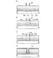
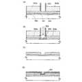
積層体に連続した開口を形成する例を図4に示す。図4(A)において、基板700上に、導電層701、第1の絶縁層708及び第2の絶縁層702が形成されている。次にチューブ703を第2の絶縁層702に挿入することによって物理的に第2の絶縁層702に第1の開口704を形成する。図4(B)の断面図においては、第2の絶縁層は、第2の絶縁層706aと第2の絶縁層706bとに分離される。チューブ703の吐出口の大きさによっては、チューブ703内部に第2の絶縁層702の一部が入る場合は、さらにチューブより処理剤(エッチングガス又はエッチング液)を吐出し、内部に進入した第2の絶縁層702を除去すればよい。An example of forming continuous openings in the laminate is shown in FIG. 4A, a
チューブ703からエッチングガス709を吐出してさらに第1の絶縁層を選択的に除去し、第1の絶縁層及び第2の絶縁層に連続した第2の開口705を形成することができる。図4(C)の断面図においては、第1の絶縁層は、第1の絶縁層790aと第1の絶縁層790bとに分離される。An
開口705は、チューブの形状を反映するため、側面に段差を有する形状となる。導電層701が露出された第2の開口705に導電膜707を形成し、導電層701と導電膜707とを電気的に接続することができる(図4(D)参照。)。The
つまりチューブの物理的な力で第1の開口を形成し、チューブより吐出(噴出)されるエッチングガスの化学的な力によって第2の開口を形成してもよい。先にチューブよりエッチングガスを吐出して、第1の開口を形成し、チューブを絶縁層に挿入して第2の開口を形成してもよいし、エッチングガスを吐出しながら同時にチューブを絶縁層に挿入して開口を形成してもよい。That is, the first opening may be formed by the physical force of the tube, and the second opening may be formed by the chemical force of the etching gas discharged (ejected) from the tube. The etching gas may be discharged from the tube first to form the first opening, and the tube may be inserted into the insulating layer to form the second opening. An opening may be formed by being inserted into the.
第2の絶縁層がチューブより物理的強度が弱い場合、図4のように開口を形成することができる。第2の絶縁層をスピンコートなどのウェットプロセスを用いて形成する場合、第2の絶縁層が硬化する前に開口を形成してもよい。勿論第2の絶縁層に加熱処理などを行い物理的強度を低下させて、チューブを挿入してもよい。When the second insulating layer has a physical strength weaker than that of the tube, an opening can be formed as shown in FIG. In the case where the second insulating layer is formed using a wet process such as spin coating, an opening may be formed before the second insulating layer is cured. Of course, the second insulating layer may be subjected to heat treatment or the like to reduce the physical strength, and the tube may be inserted.
図5に、図4においてチューブの先端が細い円錐形状の例を示す。基板730上に、導電層731、第1の絶縁層738及び第2の絶縁層732が形成されている。次にチューブ733を第2の絶縁層732に挿入することによって物理的に第2の絶縁層732に第1の開口734を形成する。図5(B)の断面図においては、第2の絶縁層は、第2の絶縁層736aと第2の絶縁層736bとに分離される。FIG. 5 shows an example in which the tip of the tube in FIG. A
チューブ733の吐出口からエッチング液739を吐出してさらに第1の絶縁層738を選択的に除去し、第1の絶縁層及び第2の絶縁層に連続した第2の開口735を形成することができる。図5(C)の断面図においては、第1の絶縁層は、第1の絶縁層791aと第1の絶縁層791bとに分離される。The
開口735は、チューブの形状を反映するため、側面に段差を有する形状となる。導電層731が露出された第2の開口735に導電膜737を形成し、導電層731と導電膜737とを電気的に接続することができる(図5(D)参照。)。チューブは断面形状が導電層に向かって先端が細くなる側辺にテーパーを有する形状である。開口735は、チューブ733の形状を反映し、開口の側辺がテーパーを有する形状となっている。Since the
さらに、本発明のチューブによって絶縁層に開口を形成した後、チューブより液状の膜形成材料(例えば導電性を有する組成物)を開口に吐出し、導電層を形成してもよい。図6(A)は、図5(C)と対応しており、基板750上に導電層751が形成され、チューブ753により第1の絶縁層792a、792b、第2の絶縁層756a、756bが形成されている。チューブ753内は、第1の絶縁層材料が溶解したエッチング液759を有している。Furthermore, after forming an opening in the insulating layer with the tube of the present invention, a liquid film forming material (for example, a conductive composition) may be discharged from the tube into the opening to form a conductive layer. FIG. 6A corresponds to FIG. 5C, in which a
第1の絶縁層材料が溶解したエッチング液759を吸引により除去し、開口755を形成する(図6(B)参照。)。チューブ753より液状の導電性を有する組成物749を開口755に吐出し、導電層757を形成する(図6(C)(D)参照。)よって、導電層751と導電層757とを電気的に接続することができる。The
開口が微細であると、液状の膜形成材料は表面張力の関係より開口に確実に充填されにくい場合があるが、本発明であると、開口に挿入されたチューブによって確実に開口に膜形成材料を充填でき、形状不良なく膜を形成することができる。If the opening is fine, the liquid film-forming material may not be reliably filled into the opening due to the surface tension. However, in the present invention, the film-forming material is reliably attached to the opening by the tube inserted into the opening. The film can be formed without a shape defect.
膜形成材料を含む組成物は、形成する膜によって適宜設定すればよく、導電膜を形成する場合は、導電性材料を含む組成物とすればよい。また絶縁膜を形成する場合は、同様に絶縁性材料を含む組成物、半導体膜を形成する場合は、半導体材料を含む組成物とすればよい。また、膜形成材料を含む組成物はフッ素を有する界面活性剤を含んでもよい。The composition containing the film forming material may be set as appropriate depending on the film to be formed. When the conductive film is formed, the composition containing the conductive material may be used. Similarly, when an insulating film is formed, a composition containing an insulating material may be used. When a semiconductor film is formed, a composition containing a semiconductor material may be used. Moreover, the composition containing the film forming material may contain a surfactant having fluorine.
膜として導電膜を形成する場合、吐出する組成物は、導電性材料を溶媒に溶解又は分散させたものを用いる。導電性材料とは、Ag、Au、Cu、Ni、Pt、Pd、Ir、Rh、W、Al等の一種又は複数種の金属の微粒子又は分散性ナノ粒子に相当する。また前記導電性材料には、Cd、Znの金属硫化物、Fe、Ti、Ge、Si、Zr、Baなどの酸化物、ハロゲン化銀の一種又は複数種の微粒子又は分散性ナノ粒子を混合してもよい。また、導電性材料として、透明導電膜として用いられるインジウム錫酸化物(ITO)、酸化珪素を含むインジウム錫酸化物(ITSO)、有機インジウム、有機スズ、酸化亜鉛、窒化チタン等を用いてもよい。導電性材料は、単一元素、又は複数種の元素の粒子を混合して用いることができる。但し、吐出する組成物は、比抵抗値を考慮して、金、銀、銅のいずれかの材料を溶媒に溶解又は分散させたものを用いることが好適であり、より好適には、低抵抗な銀、銅を用いるとよい。但し、銀、銅を用いる場合には、不純物対策のため、合わせてバリア膜を設けるとよい。バリア膜としては、窒化珪素膜やニッケルボロン(NiB)を用いることができる。In the case where a conductive film is formed as a film, a discharged composition is obtained by dissolving or dispersing a conductive material in a solvent. The conductive material corresponds to fine particles or dispersible nanoparticles of one or more kinds of metals such as Ag, Au, Cu, Ni, Pt, Pd, Ir, Rh, W, and Al. Further, the conductive material is mixed with metal sulfides of Cd and Zn, oxides such as Fe, Ti, Ge, Si, Zr, and Ba, one or more kinds of fine particles of silver halide, or dispersible nanoparticles. May be. As the conductive material, indium tin oxide (ITO) used as a transparent conductive film, indium tin oxide containing silicon oxide (ITSO), organic indium, organic tin, zinc oxide, titanium nitride, or the like may be used. . As the conductive material, particles of a single element or a plurality of kinds of elements can be mixed and used. However, it is preferable to use a composition in which any one of gold, silver, and copper is dissolved or dispersed in a solvent in consideration of a specific resistance value, and more preferably a low resistance composition. It is recommended to use silver or copper. However, when silver or copper is used, a barrier film may be provided as a countermeasure against impurities. As the barrier film, a silicon nitride film or nickel boron (NiB) can be used.
吐出する組成物は、導電性材料(絶縁性材料)を溶媒に溶解又は分散させたものであるが、他にも分散剤や、バインダーと呼ばれる熱硬化性樹脂が含まれている。特にバインダーに関しては、焼成時にクラックや不均一な焼きムラが発生するのを防止する働きを持つ。よって、形成される導電層には、有機材料が含まれることがある。含まれる有機材料は、加熱温度、雰囲気、時間により異なる。この有機材料は、金属粒子のバインダー、溶媒、分散剤、及び被覆剤として機能する有機樹脂などであり、代表的には、ポリイミド、アクリル、ノボラック樹脂、メラミン樹脂、フェノール樹脂、エポキシ樹脂、シリコーン樹脂、フラン樹脂、ジアリルフタレート樹脂等の有機樹脂が挙げられる。The composition to be discharged is one obtained by dissolving or dispersing a conductive material (insulating material) in a solvent, but additionally contains a dispersant and a thermosetting resin called a binder. In particular, the binder has a function of preventing occurrence of cracks and uneven baking during firing. Thus, the formed conductive layer may contain an organic material. The organic material contained varies depending on the heating temperature, atmosphere, and time. This organic material is a binder of metal particles, a solvent, a dispersant, an organic resin that functions as a coating agent, etc., typically polyimide, acrylic, novolac resin, melamine resin, phenol resin, epoxy resin, silicone resin And organic resins such as furan resin and diallyl phthalate resin.
また、導電性材料の周りに他の導電性材料がコーティングされ、複数の層になっている粒子でも良い。例えば、銅の周りにニッケルボロン(NiB)がコーティングされ、その周囲に銀がコーティングされている3層構造の粒子などを用いても良い。溶媒は、酢酸ブチル、酢酸エチル等のエステル類、イソプロピルアルコール、エチルアルコール等のアルコール類、メチルエチルケトン、アセトン等の有機溶剤等、又は水を用いる。組成物の粘度は20mPa・s以下が好適であり、これは、吐出時に乾燥が起こることを防止、又は吐出口から組成物を円滑に吐出できるようにするためである。また、組成物の表面張力は、40mN/m以下が好適である。但し、用いる溶媒や、用途に合わせて、組成物の粘度等は適宜調整するとよい。一例として、ITOや、有機インジウム、有機スズを溶媒に溶解又は分散させた組成物の粘度は5〜20mPa・s、銀を溶媒に溶解又は分散させた組成物の粘度は5〜20mPa・s、金を溶媒に溶解又は分散させた組成物の粘度は5〜20mPa・sに設定するとよい。Alternatively, particles in which a conductive material is coated with another conductive material to form a plurality of layers may be used. For example, particles having a three-layer structure in which nickel boron (NiB) is coated around copper and silver is coated around it may be used. As the solvent, esters such as butyl acetate and ethyl acetate, alcohols such as isopropyl alcohol and ethyl alcohol, organic solvents such as methyl ethyl ketone and acetone, and water are used. The viscosity of the composition is preferably 20 mPa · s or less, in order to prevent drying from occurring during discharge or to smoothly discharge the composition from the discharge port. The surface tension of the composition is preferably 40 mN / m or less. However, the viscosity and the like of the composition may be appropriately adjusted according to the solvent to be used and the application. As an example, the viscosity of a composition in which ITO, organic indium, or organic tin is dissolved or dispersed in a solvent is 5 to 20 mPa · s, the viscosity of a composition in which silver is dissolved or dispersed in a solvent is 5 to 20 mPa · s, The viscosity of the composition in which gold is dissolved or dispersed in a solvent is preferably set to 5 to 20 mPa · s.
膜として絶縁層を形成する場合は、エポキシ樹脂、フェノール樹脂、ノボラック樹脂、アクリル樹脂、メラミン樹脂、ウレタン樹脂、ベンゾシクロブテン、パリレン、フッ化アリーレンエーテル、ポリイミドなどの有機材料、シロキサン結合を有する樹脂を用いることができる。いずれの材料を用いるとしても、その表面張力と粘度は、溶媒の濃度を調整する、界面活性剤等を加えるなどを行い適宜調整する。When an insulating layer is formed as a film, an epoxy resin, a phenol resin, a novolac resin, an acrylic resin, a melamine resin, a urethane resin, an organic material such as benzocyclobutene, parylene, fluorinated arylene ether, a resin having a siloxane bond Can be used. Regardless of which material is used, its surface tension and viscosity are appropriately adjusted by adjusting the concentration of the solvent, adding a surfactant or the like.
チューブの径や所望のパターン形状などに依存するが、チューブの目詰まり防止や高精細なパターンの作製のため、導電体の粒子の径はなるべく小さい方が好ましく、好適には粒径0.1μm以下が好ましい。組成物は、電解法、アトマイズ法又は湿式還元法等の各種方法で形成されるものであり、その粒子サイズは、一般的に約0.01〜10μmである。但し、ガス中蒸発法で形成すると、分散剤で保護されたナノ粒子は約7nmと微細であり、またこのナノ粒子は、被覆剤を用いて各粒子の表面を覆うと、溶剤中に凝集がなく、室温で安定に分散し、液体とほぼ同じ挙動を示す。従って、被覆剤を用いることが好ましい。Although depending on the diameter of the tube and the desired pattern shape, the diameter of the conductor particles is preferably as small as possible to prevent clogging of the tube and the production of a high-definition pattern. The following is preferred. The composition is formed by various methods such as an electrolytic method, an atomizing method, or a wet reduction method, and its particle size is generally about 0.01 to 10 μm. However, when formed by a gas evaporation method, the nanoparticles protected by the dispersant are as fine as about 7 nm, and these nanoparticles are aggregated in the solvent when the surface of each particle is covered with a coating agent. And stably disperse at room temperature and shows almost the same behavior as liquid. Therefore, it is preferable to use a coating agent.
また、組成物を吐出する工程は、減圧下で行ってもよい。吐出時に基板を加熱しておいてもよい。組成物を吐出後、乾燥と焼成の一方又は両方の工程を行う。乾燥と焼成の工程は、両工程とも加熱処理の工程であるが、例えば、乾燥は100度(℃)で3分間、焼成は200〜550度(℃)で15分間〜60分間で行うもので、その目的、温度と時間が異なるものである。乾燥の工程、焼成の工程は、常圧下又は減圧下で、レーザ光の照射や瞬間熱アニール、加熱炉などにより行う。なお、この加熱処理を行うタイミング、加熱処理の回数は特に限定されない。乾燥と焼成の工程を良好に行うためには、そのときの温度は、基板の材質及び組成物の性質に依存するが、一般的には室温〜800度(℃)(好ましくは100〜550度(℃))とする。本工程により、組成物中の溶媒の揮発、又は化学的に分散剤を除去するとともに、周囲の樹脂が硬化収縮することで、ナノ粒子間を接触させ、融合と融着を加速する。The step of discharging the composition may be performed under reduced pressure. The substrate may be heated at the time of discharge. After discharging the composition, one or both steps of drying and baking are performed. The drying and firing steps are both heat treatment steps. For example, drying is performed at 100 degrees (C) for 3 minutes, and firing is performed at 200 to 550 degrees (C) for 15 minutes to 60 minutes. Its purpose, temperature and time are different. The drying process and the firing process are performed under normal pressure or reduced pressure by laser light irradiation, rapid thermal annealing, a heating furnace, or the like. Note that the timing of performing this heat treatment and the number of heat treatments are not particularly limited. In order to perform the drying and firing steps satisfactorily, the temperature at that time depends on the material of the substrate and the properties of the composition, but is generally room temperature to 800 ° C. (preferably 100 to 550 ° C.). (° C)). By this step, the solvent in the composition is volatilized or the dispersant is chemically removed, and the surrounding resin is cured and contracted to bring the nanoparticles into contact with each other, thereby accelerating fusion and fusion.
レーザ光の照射は、連続発振またはパルス発振の気体レーザ又は固体レーザを用いれば良い。前者の気体レーザとしては、エキシマレーザ、Arレーザ等が挙げられ、後者の固体レーザとしては、Cr、Nd等がドーピングされたYAG、YVO4、GdVO4等の結晶を使ったレーザ等が挙げられる。なお、レーザ光の吸収率の関係から、連続発振のレーザを用いることが好ましい。また、パルス発振と連続発振を組み合わせたレーザ照射方法を用いてもよい。但し、基板の耐熱性に依っては、レーザ光の照射による加熱処理は、該基板を破壊しないように、数マイクロ秒から数十秒の間で瞬間的に行うとよい。瞬間熱アニール(RTA)は、不活性ガスの雰囲気下で、紫外光乃至赤外光を照射する赤外ランプやハロゲンランプなどを用いて、急激に温度を上昇させ、数分〜数マイクロ秒の間で瞬間的に熱を加えて行う。この処理は瞬間的に行うために、実質的に最表面の薄膜のみを加熱することができ、下層の膜には影響を与えない。つまり、プラスチック基板等の耐熱性が弱い基板にも影響を与えない。For the laser light irradiation, a continuous wave or pulsed gas laser or solid-state laser may be used. Examples of the former gas laser include an excimer laser and an Ar laser, and examples of the latter solid-state laser include a laser using a crystal such as YAG, YVO4 or GdVO4 doped with Cr, Nd, or the like. . Note that it is preferable to use a continuous wave laser because of the absorption rate of the laser light. Further, a laser irradiation method combining pulse oscillation and continuous oscillation may be used. However, depending on the heat resistance of the substrate, the heat treatment by laser light irradiation may be performed instantaneously within a few microseconds to several tens of seconds so as not to destroy the substrate. Instantaneous thermal annealing (RTA) uses an infrared lamp or a halogen lamp that irradiates ultraviolet light or infrared light in an inert gas atmosphere, and rapidly raises the temperature for several minutes to several microseconds. This is done by applying heat instantaneously. Since this treatment is performed instantaneously, only the outermost thin film can be heated substantially without affecting the lower layer film. That is, it does not affect a substrate having low heat resistance such as a plastic substrate.
また、導電層などを組成物を吐出し形成した後、その平坦性を高めるために表面を圧力によってプレスして平坦化してもよい。プレスの方法としては、ローラー状のものを表面に走査する、又は平坦な板状な物で表面を垂直にプレスするなどにより、表面の凹凸を平坦化することができる。プレスする時に、加熱工程を行っても良い。また溶剤等によって表面を軟化、または融解させエアナイフで表面の凹凸部を除去しても良い。また、CMP法を用いて研磨しても良い。In addition, after the conductive layer or the like is formed by discharging a composition, the surface may be flattened by pressing with a pressure in order to enhance the flatness. As a pressing method, surface irregularities can be flattened by scanning a roller-like object on the surface or pressing the surface vertically with a flat plate-like object. A heating step may be performed when pressing. Alternatively, the surface may be softened or melted with a solvent or the like, and the surface irregularities may be removed with an air knife. Further, polishing may be performed using a CMP method.
このように導電性材料、又は絶縁性材料を含む組成物を吐出し、焼成することによって形成された導電層(または絶縁層)においては、スパッタ法などで形成した導電層(または絶縁層)が、多くは柱状構造を示すのに対し、多くの粒界を有する多結晶状態を示すことが多い。In such a conductive layer (or insulating layer) formed by discharging and baking a composition containing a conductive material or an insulating material, a conductive layer (or insulating layer) formed by a sputtering method or the like is used. Many exhibit a columnar structure, but often exhibit a polycrystalline state having many grain boundaries.
チューブより吐出される処理剤(エッチングガス又はエッチング液)は、チューブが耐えられるものであればエッチングする薄膜によって適宜選択することができる。例えば、図14及び図36のように幾層にも積層する多層配線などを作製する場合、何層にもわたって異なる薄膜に連続的な開口を形成する際に本発明を用いることができる。The treatment agent (etching gas or etchant) discharged from the tube can be appropriately selected depending on the thin film to be etched as long as the tube can withstand. For example, in the case of manufacturing a multilayer wiring or the like that is stacked in layers as shown in FIGS. 14 and 36, the present invention can be used when forming continuous openings in different thin films over several layers.
図14(A)において、基板540上に、導電層541、第1の絶縁層548及び第2の絶縁層542が形成されている。第2の絶縁層542の開口形成領域にチューブ543を第2の絶縁層542に接して設ける。チューブ543を選択的に設けた状態でそのチューブ543を通して第1のエッチングガス551を第2の絶縁層542に吐出(噴出)する。吐出(噴出)された第1のエッチングガス551によって、第2の絶縁層542を選択的に除去し、第2の絶縁層542に第1の開口544を形成する(図14(B)参照。)。図14(B)の断面図においては、第2の絶縁層は、第2の絶縁層546aと第2の絶縁層546bとに分離される。In FIG. 14A, a
チューブ543の吐出口から第2のエッチングガス549を噴出してさらに第1の絶縁層548を選択的に除去し、第1の絶縁層及び第2の絶縁層に連続した第2の開口545を形成することができる。図14(C)の断面図においては、第1の絶縁層は、第1の絶縁層550aと第1の絶縁層550bとに分離される。The
導電層541が露出された第2の開口545に導電膜547を形成し、導電層541と導電膜547とを電気的に接続することができる(図14(D)参照。)。A
図36は、基板780上に導電層781、絶縁層788を形成し、導電層795a、絶縁層782a、導電層795b、絶縁層782bが積層されている。チューブ783によって、導電層795a、絶縁層782a、導電層795b、絶縁層782bに連続した第1の開口784を形成する(図36(B)参照。)。断面図である図36(B)において、導電層796a、絶縁層786a、導電層796b、絶縁層786bが第1の開口784を有して設けられている。36, a
チューブ783からエッチングガス789を吐出(噴出)して絶縁層788を選択的に除去し、絶縁層786とし、積層した絶縁層及び導電層に連続した第2の開口785を形成することができる。The insulating
導電層781が露出された第2の開口785に導電膜787を形成し、導電層781、796a、796b及び導電膜787を電気的に接続することができる(図36(D)参照。)。A
チューブの形状において、他の例を図7(A)乃至(E)に示す。図7(A)において、基板760上に導電層761、第1の絶縁層762、第2の絶縁層768が積層されている。Another example of the shape of the tube is shown in FIGS. In FIG. 7A, a
図7(B)において、異なる断面形状を有するチューブ763a乃至763dにより、第2の絶縁層768に第1の開口770a乃至770dを形成し、絶縁層769とする。チューブ763aは、凸部先端が丸みを帯びたドーム上の形状であり、チューブ763bはチューブ先端が尖った針状形状である。チューブ763cとチューブ763dは柱状形状であるが、大きさが異なっており、チューブ763cの方がチューブ763dより細い。In FIG. 7B,
次に、チューブ763a乃至763dよりそれぞれエッチング液771a、771b、エッチングガス772a、772bを吐出し、第1の絶縁層762を選択的に除去して、第1の絶縁層773とする(図7(C)参照。)。チューブ763a乃至763dを除去し、第2の開口765a乃至765dを形成する(図7(D)参照。)。Next,
導電層761が露出された第2の開口765a乃至765dに導電膜767を形成し、導電層761と導電膜767とをそれぞれの開口765a乃至765dにおいて電気的に接続することができる(図7(E)参照。)。A
開口765a乃至765dはチューブ763a乃至763dの形状を反映した形状に形成され、絶縁層769において、開口765aは、開口底面に向かって丸みを帯びた形状であり、開口765bは底面に向かって開口の径が細くなり、先端が尖った針状形状である。開口765cと開口765dは、大きさが異なっており、開口765cの方が開口765dより小さな開口が形成されている。このように異なる形状の複数の開口を有する絶縁層を同一工程で簡便に作製することができる。従って、多様の開口形状が選択できるため、表示装置や半導体装置に含まれる配線等の構成の設計の自由度が向上する。The
また開口の深さ方向はチューブを設ける時の力と、チューブが設置される膜の膜強度によって設定することができる。先端の尖った針状のチューブを用いて、膜に一部埋め込むようにチューブを設置すると、膜に凹部を有する開口を形成することができる。The depth direction of the opening can be set by the force when the tube is provided and the film strength of the film on which the tube is installed. When a tube is installed so as to be partially embedded in the membrane using a needle-like tube having a sharp tip, an opening having a recess in the membrane can be formed.
開口を形成した後、液体で開口付近に残存する導電性材料や絶縁性材料(導電層又は絶縁層の除去された部分の残存物)を洗浄し、残存物を除去してもよい。この場合、洗浄に水などの無反応物質を用いてもよいし、絶縁層と反応する(溶解する)エッチング液などの薬液を用いてもよい。エッチング液を用いると開口がオーバーエッチングされ、ゴミ等が除去され表面がより平坦化される。また開口を広げることもできる。After the opening is formed, the conductive material or insulating material remaining in the vicinity of the opening with a liquid (residue of the removed portion of the conductive layer or the insulating layer) may be washed to remove the residue. In this case, an unreacted substance such as water may be used for cleaning, or a chemical solution such as an etching solution that reacts (dissolves) with the insulating layer may be used. When an etching solution is used, the opening is over-etched, dust and the like are removed, and the surface is flattened. The opening can also be widened.
このように複雑なフォトリソグラフィ工程、レジストマスク層の形成を行うことなく、導電層と導電層とを電気的に接続する開口(コンタクトホール)を絶縁層に形成することができる。Thus, an opening (contact hole) for electrically connecting the conductive layer and the conductive layer can be formed in the insulating layer without performing a complicated photolithography process and formation of a resist mask layer.
従って、本実施の形態によれば、絶縁層にマスクを形成することなくコンタクトホールを形成することができるので、工程を簡略化することができる。また、フォトレジスト等を塗布して露光及び現像する必要がないので、加工に必要な原材料コストを削減することができる。さらに、コンタクトホールを確実に形成することができるので、製造歩留まりの向上を図ることができる。Therefore, according to this embodiment mode, a contact hole can be formed without forming a mask in the insulating layer, so that the process can be simplified. In addition, since it is not necessary to apply a photoresist or the like for exposure and development, it is possible to reduce raw material costs required for processing. Furthermore, since the contact hole can be reliably formed, the manufacturing yield can be improved.
(実施の形態3)
本実施の形態では、簡略化した工程で低コストに作製することを目的とした表示装置の作製方法について、図35を用いて説明する。(Embodiment 3)
In this embodiment, a method for manufacturing a display device, which is intended to be manufactured at a low cost with a simplified process, will be described with reference to FIGS.
本実施の形態では、薄膜を所望のパターンに加工する際にフォトリソグラフィ工程を用いることなく導電層、半導体層などの構成物(パターンともいう)を選択的に所望の形状を有するように形成する。本発明において、構成物(パターンともいう)とは、薄膜トランジスタや表示装置を構成する、配線層、ゲート電極層、ソース電極層、ドレイン電極層などの導電層、半導体層、マスク層、絶縁層などをいい、所定の形状を有して形成される全ての構成要素を含む。In this embodiment mode, a structure (also referred to as a pattern) such as a conductive layer and a semiconductor layer is selectively formed to have a desired shape without using a photolithography process when the thin film is processed into a desired pattern. . In the present invention, a component (also referred to as a pattern) refers to a conductive layer such as a wiring layer, a gate electrode layer, a source electrode layer, and a drain electrode layer, a semiconductor layer, a mask layer, an insulating layer, etc. that constitute a thin film transistor or a display device. Including all components formed with a predetermined shape.
本実施の形態では、導電膜や半導体膜などの光吸収膜を透光性の転置基板に形成し、転置基板側よりレーザ光を選択的に照射することによって、被転置基板にレーザ光の照射領域に対応する光吸収膜を、被転置基板に転置し、光吸収層である導電層や半導体層を所望の形状(パターン)で形成する。本明細書において、最初の工程で光吸収膜である導電膜や半導体膜を形成し、レーザ光を照射される基板を転置基板、最終的に選択的に光吸収層である導電層や半導体層が形成される基板を被転置基板ともいう。フォトリソグラフィ工程を用いることなく選択的に所望の形状を有するように形成することができるため、工程簡略化、低コスト化などが達成できる。In this embodiment mode, a light-absorbing film such as a conductive film or a semiconductor film is formed over a translucent transfer substrate, and laser light is irradiated to the transfer substrate by selectively irradiating laser light from the transfer substrate side. A light absorption film corresponding to the region is transferred to the transfer substrate, and a conductive layer or a semiconductor layer which is a light absorption layer is formed in a desired shape (pattern). In this specification, a conductive film or a semiconductor film which is a light absorption film is formed in the first step, a substrate to be irradiated with laser light is a transfer substrate, and finally a conductive layer or a semiconductor layer which is a light absorption layer selectively. The substrate on which is formed is also referred to as a transferred substrate. Since a desired shape can be selectively formed without using a photolithography process, process simplification, cost reduction, and the like can be achieved.
本実施の形態で示す薄膜の形成方法を、図35を用いて詳細に説明する。図35において、転置基板である第1の基板2201上に光吸収膜2202が形成され、光吸収膜2202が内側になるように、第1の基板2201及び被転置基板である第2の基板2200が対向して設置されている。A method for forming a thin film described in this embodiment will be described in detail with reference to FIGS. In FIG. 35, a
基板2201側より、基板2201を透過させレーザ光2203を選択的に光吸収膜2202に照射する。レーザ光2203が照射された領域の光吸収膜2202は、レーザ光2203を吸収し、その熱などのエネルギーにより第2の基板2200側に光吸収層2205として転置される。一方、レーザ光2203が照射されなかった領域は、光吸収膜2204a、2204bとして第1の基板2201側に残存する。このように、光吸収層2206である薄膜を所望のパターンに加工する際にフォトリソグラフィ工程を用いることなく、導電層、半導体層などの構成物(パターンともいう)を選択的に所望の形状を有するように形成する。From the
レーザ光により転置後、光吸収層に加熱処理を行ってもよく、レーザ光を照射してもよい。After the transfer with the laser beam, the light absorption layer may be subjected to heat treatment or may be irradiated with the laser beam.
転置物である光吸収膜2202には、照射される光を吸収する材料を用い、第1の基板2201には照射される光を透過する、透光性の基板を用いる。本発明を用いると、自由に様々な基板に転置することができるため、基板の材料の選択性の幅が広がる。また安価な材料を基板として選択することもでき、用途に合わせて広い機能を持たせることができるだけでなく、低コストで表示装置を作製することができる。A light-absorbing
本実施の形態の薄膜形成方法は、薄膜トランジスタや表示装置を構成する、配線層、ゲート電極層、ソース電極層、ドレイン電極層などの導電層、半導体層、マスク層、絶縁層などの形成に用いることができ、光吸収膜として所望の材料を用いた膜を形成し、その膜が吸収する光を選択し、照射すればよい。The thin film formation method of this embodiment is used for forming a conductive layer such as a wiring layer, a gate electrode layer, a source electrode layer, and a drain electrode layer, a semiconductor layer, a mask layer, an insulating layer, and the like which constitute a thin film transistor or a display device. A film using a desired material can be formed as the light absorption film, and light absorbed by the film can be selected and irradiated.
例えば、光吸収膜として導電性材料を用いることができ、例えば、クロム、タンタル、銀、モリブデン、ニッケル、チタン、コバルト、銅、又はアルミニウムのうち一種又は複数を用いて形成することができる。また、インジウム錫酸化物(ITO)、酸化珪素を含むインジウム錫酸化物(ITSO)、酸化亜鉛(ZnO)、酸化亜鉛にガリウム(Ga)をドープした導電性材料、インジウム亜鉛酸化物(IZO(indium zinc oxide))を用いても良い。また、光吸収膜として半導体材料を用いることもでき、例えば、シリコン(珪素)、ゲルマニウム、シリコンゲルマニウム、ガリウム砒素、酸化モリブデン、酸化スズ、酸化ビスマス、酸化バナジウム、酸化ニッケル、酸化亜鉛、ヒ化ガリウム、窒化ガリウム、酸化インジウム、リン化インジウム、窒化インジウム、硫化カドミウム、テルル化カドミウム、チタン酸ストロンチウムなどの無機半導体材料を用いることができる。また光吸収膜に水素や不活性気体(ヘリウム(He)、アルゴン(Ar)、クリプトン(Kr)、ネオン(Ne)、キセノン(Xe)など)を添加してもよい。For example, a conductive material can be used for the light absorption film, and for example, one or more of chromium, tantalum, silver, molybdenum, nickel, titanium, cobalt, copper, or aluminum can be used. Indium tin oxide (ITO), indium tin oxide containing silicon oxide (ITSO), zinc oxide (ZnO), a conductive material in which zinc oxide is doped with gallium (Ga), indium zinc oxide (IZO (indium) zinc oxide)) may be used. A semiconductor material can also be used as the light absorption film, for example, silicon (silicon), germanium, silicon germanium, gallium arsenide, molybdenum oxide, tin oxide, bismuth oxide, vanadium oxide, nickel oxide, zinc oxide, gallium arsenide. Inorganic semiconductor materials such as gallium nitride, indium oxide, indium phosphide, indium nitride, cadmium sulfide, cadmium telluride, and strontium titanate can be used. Further, hydrogen or an inert gas (such as helium (He), argon (Ar), krypton (Kr), neon (Ne), or xenon (Xe)) may be added to the light absorption film.
従って、本実施の形態によれば、絶縁層にマスクを形成することなくコンタクトホールを形成することができるので、工程を簡略化することができる。また、フォトレジスト等を塗布して露光及び現像する必要がないので、加工に必要な原材料コストを削減することができる。さらに、コンタクトホールを確実に形成することができるので、製造歩留まりの向上を図ることができる。Therefore, according to this embodiment mode, a contact hole can be formed without forming a mask in the insulating layer, so that the process can be simplified. In addition, since it is not necessary to apply a photoresist or the like for exposure and development, it is possible to reduce raw material costs required for processing. Furthermore, since the contact hole can be reliably formed, the manufacturing yield can be improved.
(実施の形態4)
図25(A)は本発明に係る表示パネルの構成を示す平面図であり、絶縁表面を有する基板2700上に画素2702をマトリクス上に配列させた画素部2701、走査線側入力端子2703、信号線側入力端子2704が形成されている。画素数は種々の規格に従って設ければ良く、XGAであってRGBを用いたフルカラー表示であれば1024×768×3(RGB)、UXGAであってRGBを用いたフルカラー表示であれば1600×1200×3(RGB)、フルスペックハイビジョンに対応させ、RGBを用いたフルカラー表示であれば1920×1080×3(RGB)とすれば良い。(Embodiment 4)
FIG. 25A is a plan view showing a structure of a display panel according to the present invention. A
画素2702は、走査線側入力端子2703から延在する走査線と、信号線側入力端子2704から延在する信号線とが交差することで、マトリクス状に配設される。画素2702のそれぞれには、スイッチング素子とそれに接続する画素電極が備えられている。スイッチング素子の代表的な一例はTFTであり、TFTのゲート電極側が走査線と、ソース若しくはドレイン側が信号線と接続されることにより、個々の画素を外部から入力する信号によって独立して制御可能としている。The
図25(A)は、走査線及び信号線へ入力する信号を、外付けの駆動回路により制御する表示パネルの構成を示しているが、図26(A)に示すように、COG(Chip on Glass)方式によりドライバIC2751を保護回路2713と共に基板2700上に実装しても良い。また他の実装形態として、図26(B)に示すようなTAB(Tape Automated Bonding)方式を用いてもよい。ドライバICは単結晶半導体基板に形成されたものでも良いし、ガラス基板上にTFTで回路を形成したものであっても良い。図26において、ドライバIC2751は、FPC2750と接続している。FIG. 25A shows the structure of a display panel in which signals input to the scan lines and signal lines are controlled by an external driver circuit. As shown in FIG. 26A, COG (Chip on The
また、画素に設けるTFTを、結晶性が高い多結晶(微結晶)半導体で形成する場合には、図25(B)に示すように走査線側駆動回路3702を基板3700上に形成することもできる。図25(B)において、3701は画素部であり、3704は信号線側入力端子であり、信号線側駆動回路は、図25(A)と同様に外付けの駆動回路により制御する。本発明で形成するTFTのように、画素に設けるTFTを移動度の高い、多結晶(微結晶)半導体、単結晶半導体などで形成する場合は、図25(C)は、走査線駆動回路4702と、信号線駆動回路4704を画素部4701と共に基板4700上に一体形成することもできる。In the case where a TFT provided for a pixel is formed using a polycrystalline (microcrystalline) semiconductor with high crystallinity, a scan
本発明の実施の形態について、図8乃至図13を用いて説明する。より詳しくは、本発明を適用した、逆スタガ型の薄膜トランジスタを有する表示装置の作製方法について説明する。図8乃至図12の(A)は表示装置画素部の平面図であり、図8乃至図12の(B)は、図8乃至図12の(A)における線A−Cによる断面図、(C)は線B−Dによる断面図である。図13(A)(B)も表示装置の断面図である。An embodiment of the present invention will be described with reference to FIGS. More specifically, a method for manufacturing a display device having an inverted staggered thin film transistor to which the present invention is applied will be described. 8A to 12A are plan views of the display device pixel portion, and FIG. 8B to FIG. 12B are cross-sectional views taken along line A-C in FIG. 8A to FIG. C) is a sectional view taken along line BD. 13A and 13B are also cross-sectional views of the display device.
基板100は、バリウムホウケイ酸ガラス、アルミノホウケイ酸ガラス等からなるガラス基板、石英基板、金属基板、又は本作製工程の処理温度に耐えうる耐熱性を有するプラスチック基板を用いる。また、基板100の表面が平坦化されるようにCMP法などによって、研磨しても良い。なお、基板100上に、絶縁層を形成してもよい。絶縁層は、CVD法、プラズマCVD法、スパッタリング法、スピンコート法等の種々の方法により、珪素を含む酸化物材料、窒化物材料を用いて、単層又は積層して形成される。この絶縁層は、形成しなくても良いが、基板100からの汚染物質などを遮断する効果がある。As the
基板100上に、ゲート電極層103、104(104a、104b)を形成する。ゲート電極層103、104(104a、104b)は、Ag、Au、Ni、Pt、Pd、Ir、Rh、Ta、W、Ti、Mo、Al、Cuから選ばれた元素、又は前記元素を主成分とする合金材料もしくは化合物材料で形成すればよい。また、リン等の不純物元素をドーピングした多結晶シリコン膜に代表される半導体膜や、AgPdCu合金を用いてもよい。また、単層構造でも複数層の構造でもよく、例えば、窒化タングステン膜とモリブデン(Mo)膜との2層構造としてもよいし、膜厚50nmのタングステン膜、膜厚500nmのアルミニウムとシリコンの合金(Al−Si)膜、膜厚30nmの窒化チタン膜を順次積層した3層構造としてもよい。また、3層構造とする場合、第1の導電膜のタングステンに代えて窒化タングステンを用いてもよいし、第2の導電膜のアルミニウムとシリコンの合金(Al−Si)膜に代えてアルミニウムとチタンの合金膜(Al−Ti)を用いてもよいし、第3の導電膜の窒化チタン膜に代えてチタン膜を用いてもよい。Gate electrode layers 103 and 104 (104a and 104b) are formed over the
ゲート電極層103、104a、104bは、スパッタリング法、PVD法(Physical Vapor Deposition)、減圧CVD法(LPCVD法)、またはプラズマCVD法等のCVD法(Chemical Vapor Deposition)などを用いて形成し、マスク層を用いて加工して形成することができる。また、構成物が所望のパターンに転写、または描写できる方法、例えば各種印刷法(スクリーン(孔版)印刷、オフセット(平版)印刷、凸版印刷やグラビア(凹版)印刷など所望なパターンで形成される方法)、液滴吐出法、ディスペンサ法、選択的な塗布法なども用いることができる。The gate electrode layers 103, 104a, and 104b are formed using a sputtering method, a PVD method (Physical Vapor Deposition), a low pressure CVD method (LPCVD method), a CVD method (Chemical Vapor Deposition) such as a plasma CVD method, and the like. It can be formed by processing using a layer. In addition, a method in which the composition can be transferred or drawn in a desired pattern, for example, various printing methods (screen (stencil) printing, offset (flat plate) printing, letterpress printing, gravure (intaglio printing), etc.) ), A droplet discharge method, a dispenser method, a selective coating method, and the like can also be used.
導電膜の加工は、ドライエッチングまたはウェットエッチングによりエッチング加工すればよい。ICP(Inductively Coupled Plasma:誘導結合型プラズマ)エッチング法を用い、エッチング条件(コイル型の電極に印加される電力量、基板側の電極に印加される電力量、基板側の電極温度等)を適宜調節することにより、電極層をテーパー形状にエッチングすることができる。なお、エッチング用ガスとしては、Cl2、BCl3、SiCl4もしくはCCl4などを代表とする塩素系ガス、CF4、SF6もしくはNF3などを代表とするフッ素系ガス又はO2を適宜用いることができる。The conductive film may be processed by dry etching or wet etching. Using an ICP (Inductively Coupled Plasma) etching method, the etching conditions (the amount of power applied to the coil-type electrode, the amount of power applied to the substrate-side electrode, the electrode temperature on the substrate side, etc.) are appropriately set. By adjusting, the electrode layer can be etched into a tapered shape. As an etching gas, a chlorine-based gas typified by Cl2 , BCl3 , SiCl4, CCl4, etc., a fluorine-based gas typified by CF4 , SF6, NF3, etc., or O2 is appropriately used. be able to.
また、ゲート電極層の形成は、転置基板上に光吸収膜である導電膜を形成後、レーザ光によって選択的に被転置基板へ所望の形状に加工して形成してもよい。レーザ光により転置後、光吸収層に加熱処理を行ってもよく、レーザ光を照射してもよい。Alternatively, the gate electrode layer may be formed by forming a conductive film that is a light absorption film over the transfer substrate and then selectively processing the transfer electrode into a desired shape using a laser beam. After the transfer with the laser beam, the light absorption layer may be subjected to heat treatment or may be irradiated with the laser beam.
転置物である光吸収膜には、照射される光を吸収する材料を用い、転置基板には照射される光を透過する、透光性の基板を用いる。本発明を用いると、自由に様々な基板に転置することができるため、基板の材料の選択性の幅が広がる。また安価な材料を基板として選択することもでき、用途に合わせて広い機能を持たせることができるだけでなく、低コストで表示装置を作製することができる。A light-absorbing film, which is a transposed object, uses a material that absorbs irradiated light, and a translucent substrate that transmits the irradiated light is used for the transposed substrate. When the present invention is used, the substrate can be freely transferred to various substrates, so that the range of substrate material selectivity is widened. In addition, an inexpensive material can be selected as the substrate, so that not only a wide function can be provided depending on the application, but also a display device can be manufactured at low cost.
次に、ゲート電極層103、104(104a、104b)の上にゲート絶縁層105を形成する(図8(A)乃至(C)参照。)。ゲート絶縁層105としては、珪素の酸化物材料又は窒化物材料等の材料で形成すればよく、積層でも単層でもよい。本実施の形態では、窒化珪素膜、酸化珪素膜の2層の積層を用いる。またそれらや、酸化窒化珪素膜の単層、3層以上からなる積層でも良い。好適には、緻密な膜質を有する窒化珪素膜を用いるとよい。また、液滴吐出法で形成される導電層に銀や銅などを用いる場合、その上にバリア膜として窒化珪素膜やNiB膜を形成すると、不純物の拡散を防ぎ、表面を平坦化する効果がある。なお、低い成膜温度でゲートリーク電流の少ない緻密な絶縁膜を形成するには、アルゴンなどの希ガス元素を反応ガスに含ませ、形成される絶縁膜中に混入させると良い。Next, the
エッチング加工を用いる場合はプラズマエッチング(ドライエッチング)又はウエットエッチングのどちらを採用しても良いが、大面積基板を処理するにはプラズマエッチングが適している。エッチングガスとしては、CF4、NF3、Cl2、BCl3、などのフッ素系又は塩素系のガスを用い、HeやArなどの不活性ガスを適宜加えても良い。また、大気圧放電のエッチング加工を適用すれば、局所的な放電加工も可能であり、基板の全面にマスク層を形成する必要はない。When etching is used, either plasma etching (dry etching) or wet etching may be employed, but plasma etching is suitable for processing a large area substrate. As an etching gas, a fluorine-based or chlorine-based gas such as CF4 , NF3 , Cl2 , or BCl3 may be used, and an inert gas such as He or Ar may be appropriately added. Further, if an atmospheric pressure discharge etching process is applied, a local electric discharge process is possible, and it is not necessary to form a mask layer on the entire surface of the substrate.
次に半導体層を形成する。一導電性型を有する半導体層は必要に応じて形成すればよい。またn型を有する半導体層を形成し、nチャネル型TFTのNMOS構造、p型を有する半導体層を形成したpチャネル型TFTのPMOS構造、nチャネル型TFTとpチャネル型TFTとのCMOS構造を作製することができる。また、導電性を付与するために、導電性を付与する元素をドーピングによって添加し、不純物領域を半導体層に形成することで、nチャネル型TFT、pチャネル型TFTを形成することもできる。n型を有する半導体層を形成するかわりに、PH3ガスによるプラズマ処理を行うことによって、半導体層に導電性を付与してもよい。Next, a semiconductor layer is formed. A semiconductor layer having one conductivity type may be formed as necessary. In addition, an n-type semiconductor layer is formed, an n-channel TFT NMOS structure, a p-channel TFT PMOS structure having a p-type semiconductor layer, and an n-channel TFT and p-channel TFT CMOS structure. Can be produced. Further, in order to impart conductivity, an n-channel TFT or a p-channel TFT can be formed by adding an element imparting conductivity by doping and forming an impurity region in the semiconductor layer. Instead of forming an n-type semiconductor layer, conductivity may be imparted to the semiconductor layer by performing plasma treatment with a PH3 gas.
半導体層を形成する材料は、シランやゲルマンに代表される半導体材料ガスを用いて気相成長法やスパッタリング法で作製されるアモルファス半導体(以下「AS」ともいう。)、該非晶質半導体を光エネルギーや熱エネルギーを利用して結晶化させた多結晶半導体、或いはセミアモルファス(微結晶若しくはマイクロクリスタルとも呼ばれる。以下「SAS」ともいう。)半導体などを用いることができる。半導体層は各種手段(スパッタ法、LPCVD法、またはプラズマCVD法等)により成膜することができる。As a material for forming the semiconductor layer, an amorphous semiconductor (hereinafter also referred to as “AS”) manufactured by a vapor deposition method or a sputtering method using a semiconductor material gas typified by silane or germane is used. A polycrystalline semiconductor crystallized using energy or thermal energy, a semi-amorphous (also referred to as microcrystal or microcrystal, hereinafter, also referred to as “SAS”) semiconductor, or the like can be used. The semiconductor layer can be formed by various means (such as sputtering, LPCVD, or plasma CVD).
SASは、非晶質と結晶構造(単結晶、多結晶を含む)の中間的な構造を有し、自由エネルギー的に安定な第3の状態を有する半導体であって、短距離秩序を持ち格子歪みを有する結晶質な領域を含んでいる。少なくとも膜中の一部の領域には、0.5〜20nmの結晶領域を観測することが出来、珪素を主成分とする場合にはラマンスペクトルが520cm−1よりも低波数側にシフトしている。X線回折では珪素結晶格子に由来するとされる(111)、(220)の回折ピークが観測される。未結合手(ダングリングボンド)の終端化するため水素またはハロゲンを少なくとも1原子%またはそれ以上含ませている。SASは、珪素を含む気体をグロー放電分解(プラズマCVD)して形成する。珪素を含む気体としては、SiH4、その他にもSi2H6、SiH2Cl2、SiHCl3、SiCl4、SiF4などを用いることが可能である。またF2、GeF4を混合させても良い。この珪素を含む気体をH2、又は、H2とHe、Ar、Kr、Neから選ばれた一種または複数種の希ガス元素で希釈しても良い。希釈率は2〜1000倍の範囲、圧力は概略0.1Pa〜133Paの範囲、電源周波数は1MHz〜120MHz、好ましくは13MHz〜60MHzである。基板加熱温度は300℃以下が好ましく、100〜200℃の基板加熱温度でも形成可能である。ここで、主に成膜時に取り込まれる不純物元素として、酸素、窒素、炭素などの大気成分に由来する不純物は1×1020cm−3以下とすることが望ましく、特に、酸素濃度は5×1019cm−3以下、好ましくは1×1019cm−3以下となるようにすることが好ましい。また、ヘリウム、アルゴン、クリプトン、ネオンなどの希ガス元素を含ませて格子歪みをさらに助長させることで安定性が増し良好なSASが得られる。また半導体層としてフッ素系ガスより形成されるSAS層に水素系ガスより形成されるSAS層を積層してもよい。SAS is a semiconductor having an intermediate structure between amorphous and crystalline structures (including single crystal and polycrystal) and having a third state that is stable in terms of free energy and has a short-range order and a lattice. It includes a crystalline region with strain. A crystal region of 0.5 to 20 nm can be observed in at least a part of the film, and when silicon is a main component, the Raman spectrum is shifted to a lower wave number side than 520 cm−1. Yes. In X-ray diffraction, diffraction peaks of (111) and (220) that are derived from the silicon crystal lattice are observed. In order to terminate dangling bonds (dangling bonds), hydrogen or halogen is contained at least 1 atomic% or more. SAS is formed by glow discharge decomposition (plasma CVD) of a gas containing silicon. As a gas containing silicon, SiH4 , Si2 H6 , SiH2 Cl2 , SiHCl3 , SiCl4 , SiF4, or the like can be used. Further, F2 and GeF4 may be mixed. The gas containing silicon may be diluted with H2 , or H2 and one or more kinds of rare gas elements selected from He, Ar, Kr, and Ne. The dilution rate is in the range of 2 to 1000 times, the pressure is in the range of approximately 0.1 Pa to 133 Pa, and the power supply frequency is 1 MHz to 120 MHz, preferably 13 MHz to 60 MHz. The substrate heating temperature is preferably 300 ° C. or lower, and can be formed even at a substrate heating temperature of 100 to 200 ° C. Here, as an impurity element mainly taken in at the time of film formation, impurities derived from atmospheric components such as oxygen, nitrogen, and carbon are preferably 1 × 1020 cm−3 or less, and in particular, the oxygen concentration is 5 × 10 5. It is preferable to be19 cm−3 or less, preferably 1 × 1019 cm−3 or less. Further, by adding a rare gas element such as helium, argon, krypton, or neon to further promote lattice distortion, stability is improved and a favorable SAS can be obtained. In addition, a SAS layer formed of a hydrogen-based gas may be stacked on a SAS layer formed of a fluorine-based gas as a semiconductor layer.
アモルファス半導体としては、代表的には水素化アモルファスシリコン、結晶性半導体としては代表的にはポリシリコンなどがあげられる。ポリシリコン(多結晶シリコン)には、800℃以上のプロセス温度を経て形成されるポリシリコンを主材料として用いた所謂高温ポリシリコンや、600℃以下のプロセス温度で形成されるポリシリコンを主材料として用いた所謂低温ポリシリコン、また結晶化を促進する元素などを添加し結晶化させたポリシリコンなどを含んでいる。もちろん、前述したように、セミアモルファス半導体又は半導体層の一部に結晶相を含む半導体を用いることもできる。A typical example of an amorphous semiconductor is hydrogenated amorphous silicon, and a typical example of a crystalline semiconductor is polysilicon. Polysilicon (polycrystalline silicon) is mainly made of so-called high-temperature polysilicon using polysilicon formed through a process temperature of 800 ° C. or higher as a main material, or polysilicon formed at a process temperature of 600 ° C. or lower. And so-called low-temperature polysilicon, and polysilicon crystallized by adding an element that promotes crystallization. Of course, as described above, a semi-amorphous semiconductor or a semiconductor including a crystal phase in a part of the semiconductor layer can also be used.
半導体層に、結晶性半導体層を用いる場合、その結晶性半導体層の作製方法は、各種の方法(レーザ結晶化法、熱結晶化法、またはニッケルなどの結晶化を助長する元素を用いた熱結晶化法等)を用いれば良い。また、SASである微結晶半導体をレーザ照射して結晶化し、結晶性を高めることもできる。結晶化を助長する元素を導入しない場合は、非晶質珪素膜にレーザ光を照射する前に、窒素雰囲気下500℃で1時間加熱することによって非晶質珪素膜の含有水素濃度を1×10²⁰atoms/cm3以下にまで放出させる。これは水素を多く含んだ非晶質珪素膜にレーザ光を照射すると非晶質珪素膜が破壊されてしまうからである。In the case where a crystalline semiconductor layer is used for the semiconductor layer, a method for manufacturing the crystalline semiconductor layer can be selected from various methods (laser crystallization method, thermal crystallization method, or heat using an element that promotes crystallization such as nickel. A crystallization method or the like may be used. In addition, a microcrystalline semiconductor that is a SAS can be crystallized by laser irradiation to improve crystallinity. In the case where an element for promoting crystallization is not introduced, the amorphous silicon film is heated at 500 ° C. for 1 hour in a nitrogen atmosphere before irradiating the amorphous silicon film with laser light, whereby the concentration of hydrogen contained in the amorphous silicon film is set to 1 ×. Release to 1020 atoms / cm3 or less. This is because the amorphous silicon film is destroyed when the amorphous silicon film containing a large amount of hydrogen is irradiated with laser light.
非晶質半導体層への金属元素の導入の仕方としては、当該金属元素を非晶質半導体層の表面又はその内部に存在させ得る手法であれば特に限定はなく、例えばスパッタ法、CVD法、プラズマ処理法(プラズマCVD法も含む)、吸着法、金属塩の溶液を塗布する方法を使用することができる。このうち溶液を用いる方法は簡便であり、金属元素の濃度調整が容易であるという点で有用である。また、このとき非晶質半導体層の表面の濡れ性を改善し、非晶質半導体層の表面全体に水溶液を行き渡らせるため、酸素雰囲気中でのUV光の照射、熱酸化法、ヒドロキシラジカルを含むオゾン水又は過酸化水素による処理等により、酸化膜を成膜することが望ましい。The method of introducing the metal element into the amorphous semiconductor layer is not particularly limited as long as the metal element can be present on the surface of the amorphous semiconductor layer or inside the amorphous semiconductor layer. For example, sputtering, CVD, A plasma treatment method (including a plasma CVD method), an adsorption method, or a method of applying a metal salt solution can be used. Among these, the method using a solution is simple and useful in that the concentration of the metal element can be easily adjusted. At this time, in order to improve the wettability of the surface of the amorphous semiconductor layer and to spread the aqueous solution over the entire surface of the amorphous semiconductor layer, irradiation with UV light in an oxygen atmosphere, thermal oxidation method, hydroxy radical It is desirable to form an oxide film by treatment with ozone water or hydrogen peroxide.
非晶質半導体層の結晶化は、熱処理とレーザ光照射による結晶化を組み合わせてもよく、熱処理やレーザ光照射を単独で、複数回行っても良い。The crystallization of the amorphous semiconductor layer may be a combination of heat treatment and crystallization by laser light irradiation, or may be performed multiple times by heat treatment or laser light irradiation alone.
また、結晶性半導体層を、直接基板にプラズマ法により選択的に形成しても良い。Alternatively, the crystalline semiconductor layer may be selectively formed directly over the substrate by a plasma method.
半導体として、有機半導体材料を用い、印刷法、ディスペンサ法、スプレー法、スピン塗布法、液滴吐出法などで形成することができる。この場合、上記エッチング工程が必要ないため、工程数を削減することが可能である。有機半導体としては、低分子材料、高分子材料などが用いられ、有機色素、導電性高分子材料などの材料も用いることができる。本発明に用いる有機半導体材料としては、ペンタセンや、その骨格が共役二重結合から構成されるπ電子共役系の高分子材料が望ましい。代表的には、ポリチオフェン、ポリフルオレン、ポリ(3−アルキルチオフェン)、ポリチオフェン誘導体等の可溶性の高分子材料を用いることができる。As a semiconductor, an organic semiconductor material can be used and formed by a printing method, a dispenser method, a spray method, a spin coating method, a droplet discharge method, or the like. In this case, the number of processes can be reduced because the etching process is not necessary. As the organic semiconductor, a low molecular material, a polymer material, or the like is used, and materials such as an organic dye or a conductive polymer material can also be used. The organic semiconductor material used in the present invention is preferably pentacene or a π-electron conjugated polymer material whose skeleton is composed of conjugated double bonds. Typically, a soluble polymer material such as polythiophene, polyfluorene, poly (3-alkylthiophene), or a polythiophene derivative can be used.
その他にも本発明に用いることができる有機半導体材料としては、可溶性の前駆体を成膜した後で処理することにより半導体層を形成することができる材料がある。なお、このような有機半導体材料としては、ポリチエニレンビニレン、ポリ(2,5−チエニレンビニレン)、ポリアセチレン、ポリアセチレン誘導体、ポリアリレンビニレンなどがある。In addition, as an organic semiconductor material that can be used in the present invention, there is a material that can form a semiconductor layer by processing after forming a soluble precursor. Examples of such an organic semiconductor material include polythienylene vinylene, poly (2,5-thienylene vinylene), polyacetylene, a polyacetylene derivative, and polyarylene vinylene.
前駆体を有機半導体に変換する際には、加熱処理だけではなく塩化水素ガスなどの反応触媒を添加することがなされる。また、これらの可溶性有機半導体材料を溶解させる代表的な溶媒としては、トルエン、キシレン、クロロベンゼン、ジクロロベンゼン、アニソール、クロロフォルム、ジクロロメタン、γブチルラクトン、ブチルセルソルブ、シクロヘキサン、NMP(N−メチル−2−ピロリドン)、シクロヘキサノン、2−ブタノン、ジオキサン、ジメチルホルムアミド(DMF)または、THF(テトラヒドロフラン)などを適用することができる。When converting the precursor into an organic semiconductor, a reaction catalyst such as hydrogen chloride gas is added as well as heat treatment. Typical solvents for dissolving these soluble organic semiconductor materials include toluene, xylene, chlorobenzene, dichlorobenzene, anisole, chloroform, dichloromethane, γ-butyllactone, butyl cellosolve, cyclohexane, NMP (N-methyl-2) -Pyrrolidone), cyclohexanone, 2-butanone, dioxane, dimethylformamide (DMF), THF (tetrahydrofuran), or the like can be applied.
本実施の形態では、半導体層108、109及び一導電型を有する半導体層110、111として非晶質半導体層を形成する。本実施の形態では、一導電型を有する半導体膜として、n型を付与する不純物元素であるリン(P)を含むn型を有する半導体膜を形成する。一導電型を有する半導体膜は、ソース領域及びドレイン領域として機能する。一導電型を有する半導体膜は必要に応じて形成すればよく、n型を付与する不純物元素(P、As)を有するn型を有する半導体膜やp型を付与する不純物元素(B)を有するp型を有する半導体膜を形成することができる。In this embodiment, amorphous semiconductor layers are formed as the semiconductor layers 108 and 109 and the semiconductor layers 110 and 111 having one conductivity type. In this embodiment, an n-type semiconductor film containing phosphorus (P) which is an impurity element imparting n-type conductivity is formed as the semiconductor film having one conductivity type. A semiconductor film having one conductivity type functions as a source region and a drain region. A semiconductor film having one conductivity type may be formed as necessary, and includes an n-type semiconductor film having an impurity element imparting n-type (P, As) and an impurity element imparting p-type (B). A p-type semiconductor film can be formed.
ゲート絶縁層105にゲート電極層104に達する開口107を形成する(図9(A)乃至(C)参照。)。開口107の形成は、半導体層108、109及び一導電型を有する半導体層110、111を形成する前でもよい。本実施の形態では、チューブをゲート絶縁層105の開口形成領域上にゲート絶縁層105に接して配置し、そのチューブを通してエッチングガスをゲート絶縁層105に吐出(噴出)する。吐出(噴出)されたエッチングガスによって、ゲート絶縁層105を選択的に除去し、ゲート絶縁層105に開口107を形成する。従って、ゲート電極層104上に開口を有するゲート絶縁層105が形成され、ゲート絶縁層105下のゲート電極層104が開口の底面に露出する。後工程で露出されたゲート電極層104と接するように開口107にソース電極層又はドレイン電極層を形成し、ゲート電極層とソース電極層又はドレイン電極層をゲート絶縁層105に設けられた開口107において電気的に接続する。An
また、チューブを絶縁層に一部埋め込むように配置し、物理的な力によって絶縁層に第1の開口を形成し、その後、チューブからエッチングガスを噴出してさらに絶縁層を選択的に除去し、第2の開口を形成することもできる。先にチューブよりエッチングガスを吐出して、第1の開口を形成し、チューブを絶縁層に挿入して第2の開口を形成してもよいし、エッチングガスを吐出しながら同時にチューブを絶縁層に挿入して開口を形成してもよい。In addition, the tube is arranged so as to be partially embedded in the insulating layer, the first opening is formed in the insulating layer by physical force, and then the etching gas is ejected from the tube to further remove the insulating layer selectively. A second opening can also be formed. The etching gas may be discharged from the tube first to form the first opening, and the tube may be inserted into the insulating layer to form the second opening. An opening may be formed by being inserted into the.
チューブから吐出される処理剤(エッチングガス又はエッチング液)は、チューブが耐えられるものであればエッチングする薄膜によって適宜選択することができる。例えば、幾層にも積層する多層配線などを作製する場合、何層にもわたって異なる薄膜に連続的な開口を形成する際に本発明を用いることができる。The treatment agent (etching gas or etchant) discharged from the tube can be appropriately selected depending on the thin film to be etched as long as the tube can withstand. For example, in the case of producing a multilayer wiring or the like laminated in several layers, the present invention can be used in forming continuous openings in different thin films over several layers.
さらに、本発明のチューブによって絶縁層に開口を形成した後、チューブを通して液状の膜形成材料(例えば導電性を有する組成物)を開口に吐出し、導電層を形成してもよい。開口が微細であると、液状の膜形成材料は表面張力の関係より開口に確実に充填されにくい場合があるが、本発明であると、開口に挿入されたチューブによって確実に開口に膜形成材料を充填でき、形状不良なく膜を形成することができる。Furthermore, after forming an opening in the insulating layer with the tube of the present invention, a liquid film forming material (for example, a conductive composition) may be discharged into the opening through the tube to form the conductive layer. If the opening is fine, the liquid film-forming material may not be reliably filled into the opening due to the surface tension. However, in the present invention, the film-forming material is reliably attached to the opening by the tube inserted into the opening. The film can be formed without a shape defect.
開口の形状はチューブ及びエッチング物質を吐出する吐出口の形状を反映するため、所望の形状が得られるようにチューブを設定すればよい。チューブは柱状(角柱、円柱、三角柱など)、針状などを用いることができる。また開口の深さ方向はチューブを設ける時の力と、チューブが設置される導電層の膜強度によって設定することができる。また、エッチング時間などのエッチング条件を設定することによっても膜厚方向の深さを選択できる。先端の尖った針状のチューブを用いて、導電層に一部埋め込むようにチューブを挿入し設置すると、導電層に凹部を有する開口を形成することができる。また開口形成後、開口を有する絶縁層をマスクとして開口底面に露出された導電層をエッチングによって除去してもよい。Since the shape of the opening reflects the shape of the discharge port for discharging the tube and the etching substance, the tube may be set so as to obtain a desired shape. The tube may have a columnar shape (such as a prism, a cylinder, or a triangular column), a needle shape, or the like. The depth direction of the opening can be set by the force when the tube is provided and the film strength of the conductive layer where the tube is installed. The depth in the film thickness direction can also be selected by setting etching conditions such as etching time. When a needle-like tube with a sharp tip is inserted and installed so as to be partially embedded in the conductive layer, an opening having a recess can be formed in the conductive layer. Further, after the opening is formed, the conductive layer exposed on the bottom surface of the opening may be removed by etching using the insulating layer having the opening as a mask.
本発明は、絶縁層の開口形成領域にチューブを絶縁層に接して配置する。従って、物理的に絶縁層の開口形成領域を設定できるため、確実に所望の位置に開口を形成することができる。従って、本発明を用いて半導体装置、表示装置を歩留まり良く作製することができる。In the present invention, the tube is disposed in contact with the insulating layer in the opening forming region of the insulating layer. Therefore, since the opening formation region of the insulating layer can be set physically, the opening can be surely formed at a desired position. Therefore, a semiconductor device and a display device can be manufactured with high yield by using the present invention.
本発明によってフォトリソグラフィ工程を用いることなく、選択的に薄膜に開口を形成することができるので工程及び材料を削減することができる。According to the present invention, since an opening can be selectively formed in a thin film without using a photolithography process, the number of processes and materials can be reduced.
チューブを有する吐出吸引装置の一態様を図30に示す。吐出吸引手段1403の個々のヘッド1405、ヘッド1412は制御手段1407に接続され、それがコンピュータ1410で制御することにより予めプログラミングされたパターンに移動することができる。移動するタイミング及び位置は、例えば、基板1400上に形成されたマーカー1411を基準に行えば良い。或いは、基板1400の縁を基準にして基準点を確定させても良い。これを撮像手段1404で検出し、画像処理手段1409にてデジタル信号に変換したものをコンピュータ1410で認識して制御信号を発生させて制御手段1407に送る。撮像手段1404としては、電荷結合素子(CCD)や相補型金属酸化物半導体を利用したイメージセンサなどを用いることができる。勿論、基板1400上に形成されるべき開口パターンの情報は記憶媒体1408に格納されたものであり、この情報を基にして制御手段1407に制御信号を送り、吐出吸引手段1403の個々のヘッド1405、ヘッド1412を個別に制御することができる。吐出する材料(エッチングガス、エッチング液、導電性材料、絶縁性材料)は、材料供給源1413、材料供給源1414より配管を通してヘッド1405、ヘッド1412にそれぞれ供給される。ヘッド1405、ヘッド1412には複数のチューブが設けられており、チューブにより吐出される処理剤(エッチングガス又はエッチング液)により被処理物に開口を形成することができる。また、チューブを通してエッチング液などを吸引することもでき、開口に材料を吐出し、膜を形成することも出来る。One mode of the discharge and suction device having a tube is shown in FIG. The individual heads 1405 and 1412 of the discharge /
ヘッド1405内部は、点線1406が示すように液状の材料を充填する空間と、吐出口であるノズルを有する構造となっている。図示しないが、ヘッド1412もヘッド1405と同様な内部構造を有する。ヘッド1405とヘッド1412のノズルを異なるサイズで設けると、異なる領域を異なる幅で同時に加工することができる。広領域に加工する場合は、スループットを向上させるため複数のチューブより同材料を同時に吐出し、被処理膜を加工することができる。大型基板を用いる場合、ヘッド1405、ヘッド1412は基板上を、矢印の方向に自在に走査し、加工する領域を自由に設定することができ、同じパターンを一枚の基板に複数加工することができる。The inside of the
次にソース電極層又はドレイン電極層116、117、118、119を形成する。ソース電極層又はドレイン電極層116、117、118、119は、Ag(銀)、Au(金)、Cu(銅)、W(タングステン)、Al(アルミニウム)、Mo(モリブデン)、Ta(タンタル)、Ti(チタン)から選ばれた元素、又は前記元素を主成分とする合金材料もしくは化合物材料等を用いることができる。また、透光性を有するインジウム錫酸化物(ITO)、酸化珪素を含むインジウム錫酸化物(ITSO)、有機インジウム、有機スズ、酸化亜鉛、窒化チタンなどを組み合わせても良い。Next, source or drain electrode layers 116, 117, 118, and 119 are formed. The
ソース電極層又はドレイン電極層116、117、118、119は、スパッタリング法、PVD法(Physical Vapor Deposition)、減圧CVD法(LPCVD法)、またはプラズマCVD法等のCVD法(Chemical Vapor Deposition)などを用いて形成し、マスク層を用いて加工して形成することができる。また、構成物が所望のパターンに転写、または描写できる方法、例えば各種印刷法(スクリーン(孔版)印刷、オフセット(平版)印刷、凸版印刷やグラビア(凹版)印刷など所望なパターンで形成される方法)、液滴吐出法、ディスペンサ法、選択的な塗布法なども用いることができる。The source or drain electrode layers 116, 117, 118, and 119 are formed by a sputtering method, a PVD method (Physical Vapor Deposition), a low pressure CVD method (LPCVD method), a CVD method (Chemical Vapor Deposition) such as a plasma CVD method, or the like. And can be formed by processing using a mask layer. In addition, a method in which the composition can be transferred or drawn in a desired pattern, for example, various printing methods (screen (stencil) printing, offset (flat plate) printing, letterpress printing, gravure (intaglio printing), etc.) ), A droplet discharge method, a dispenser method, a selective coating method, and the like can also be used.
導電膜の加工は、ドライエッチングまたはウェットエッチングによりエッチング加工すればよい。ICP(Inductively Coupled Plasma:誘導結合型プラズマ)エッチング法を用い、エッチング条件(コイル型の電極に印加される電力量、基板側の電極に印加される電力量、基板側の電極温度等)を適宜調節することにより、電極層をテーパー形状にエッチングすることができる。なお、エッチング用ガスとしては、Cl2、BCl3、SiCl4もしくはCCl4などを代表とする塩素系ガス、CF4、SF6もしくはNF3などを代表とするフッ素系ガス又はO2を適宜用いることができる。The conductive film may be processed by dry etching or wet etching. Using an ICP (Inductively Coupled Plasma) etching method, the etching conditions (the amount of power applied to the coil-type electrode, the amount of power applied to the substrate-side electrode, the electrode temperature on the substrate side, etc.) are appropriately set. By adjusting, the electrode layer can be etched into a tapered shape. As an etching gas, a chlorine-based gas typified by Cl2 , BCl3 , SiCl4, CCl4, etc., a fluorine-based gas typified by CF4 , SF6, NF3, etc., or O2 is appropriately used. be able to.
ソース電極層又はドレイン電極層の形成は、転置基板上に光吸収膜である導電膜を形成後、レーザ光によって選択的に被転置基板へ所望の形状に加工して形成してもよい。The source electrode layer or the drain electrode layer may be formed by forming a conductive film that is a light absorption film over the transfer substrate and then selectively processing the transfer electrode into a desired shape with a laser beam.
ソース電極層又はドレイン電極層116はソース配線層としても機能し、ソース電極層又はドレイン電極層118は電源線としても機能する。The source or drain
ゲート絶縁層105に形成した開口107において、ソース電極層又はドレイン電極層117とゲート電極層104とを電気的に接続させる。ソース電極層又はドレイン電極層118の一部は容量素子を形成する。ソース電極層又はドレイン電極層116、117、118、119を形成した後、半導体層108、109、一導電型を有する半導体層110、111を所望の形状に加工する。本実施の形態では、ソース電極層又はドレイン電極層116、117、118、119をマスクとして、半導体層108、109、一導電型を有する半導体層110、111をエッチングにより加工し、半導体層114、115、一導電型を有する半導体層120a、120b、121a、121bを形成する。In the
以上の工程で逆スタガ型薄膜トランジスタであるトランジスタ139a、139bを作製する(図10(A)乃至(C)参照。)。Through the above steps,
ゲート絶縁層105及びトランジスタ139a、139b上に絶縁層123、絶縁層127を形成する。An insulating
絶縁層123は、スパッタリング法、PVD法(Physical Vapor Deposition)、減圧CVD法(LPCVD法)、またはプラズマCVD法等のCVD法(Chemical Vapor Deposition)などにより形成することができる。また、液滴吐出法や、印刷法(スクリーン印刷やオフセット印刷などパターンが形成される方法)、スピンコート法などの塗布法、ディッピング法、ディスペンサ法などを用いることもできる。The insulating
絶縁層123、絶縁層127は、酸化珪素、窒化珪素、酸化窒化珪素、酸化アルミニウム、窒化アルミニウム、酸化窒化アルミニウム、ダイアモンドライクカーボン(DLC)、窒素含有炭素(CN)、ポリシラザン、その他の無機絶縁性材料を含む物質から選ばれた材料で形成することができる。また、シロキサンを含む材料を用いてもよい。また、有機絶縁性材料を用いてもよく、有機材料としては、ポリイミド、アクリル、ポリアミド、ポリイミドアミド、レジスト又はベンゾシクロブテンを用いることができる。また、オキサゾール樹脂を用いることもでき、例えば光硬化型ポリベンゾオキサゾールなどを用いることができる。The insulating
本実施の形態では、実施の形態1及び実施の形態2で示したように、チューブを用いて絶縁層123、127にソース電極層又はドレイン電極層119に達するコンタクトホール(開口)を形成する(図11(A)乃至(C)参照。)。In this embodiment mode, as shown in Embodiment Modes 1 and 2, a contact hole (opening) reaching the source or drain
図11(B)に示すようにチューブ124を絶縁層127に埋め込むように配置し、物理的な力によって絶縁層127に第1の開口125を形成し、その後、図11(C)に示すようにチューブ124からエッチングガス128を噴出してさらに絶縁層123を選択的に除去し、第2の開口129を形成する。よって、絶縁層123、127にソース電極層又はドレイン電極層119に達するコンタクトホール(開口)を形成することができる。As shown in FIG. 11B, the
開口の形状はチューブ及びエッチング物質を吐出する吐出口の形状を反映するため、所望の形状が得られるようにチューブを設定すればよい。チューブは柱状(角柱、円柱、三角柱など)、針状などを用いることができる。また開口の深さ方向はチューブを設ける時の力と、チューブが設置される膜の膜強度によって設定することができる。また、エッチング時間などのエッチング条件を設定することによっても膜厚方向の深さを選択できる。先端の尖った針状のチューブを用いて、導電層に一部埋め込むようにチューブを挿入し設置すると、導電層に凹部を有する開口を形成することができる。また開口形成後、開口を有する絶縁層をマスクとして開口底面に露出された導電層をエッチングによって除去してもよい。Since the shape of the opening reflects the shape of the discharge port for discharging the tube and the etching substance, the tube may be set so as to obtain a desired shape. The tube may have a columnar shape (such as a prism, a cylinder, or a triangular column), a needle shape, or the like. The depth direction of the opening can be set by the force when the tube is provided and the film strength of the film on which the tube is installed. The depth in the film thickness direction can also be selected by setting etching conditions such as etching time. When a needle-like tube with a sharp tip is inserted and installed so as to be partially embedded in the conductive layer, an opening having a recess can be formed in the conductive layer. Further, after the opening is formed, the conductive layer exposed on the bottom surface of the opening may be removed by etching using the insulating layer having the opening as a mask.
本発明は、絶縁層の開口形成領域にチューブを絶縁層に接して配置する。従って、物理的に絶縁層の開口形成領域を設定できるため、確実に所望の位置に開口を形成することができる。従って、本発明を用いて半導体装置、表示装置を歩留まり良く作製することができる。In the present invention, the tube is disposed in contact with the insulating layer in the opening forming region of the insulating layer. Therefore, since the opening formation region of the insulating layer can be set physically, the opening can be surely formed at a desired position. Therefore, a semiconductor device and a display device can be manufactured with high yield by using the present invention.
本発明によってフォトリソグラフィ工程を用いることなく、選択的に薄膜に開口を形成することができるので工程及び材料を削減することができる。According to the present invention, since an opening can be selectively formed in a thin film without using a photolithography process, the number of processes and materials can be reduced.
ソース電極層又はドレイン電極層119が露出された開口129に画素電極として機能する発光素子の第1の電極層126を形成し、ソース電極層又はドレイン電極層119と第1の電極層126とは電気的に接続することができる(図12(A)乃至(C)参照。)。A
さらに、本発明のチューブによって絶縁層123、127に開口129を形成した後、チューブ124を通して液状の膜形成材料(例えば導電性を有する組成物)を開口に吐出し、第1の電極層126を形成してもよい。開口が微細であると、液状の膜形成材料は表面張力の関係より開口に確実に充填されにくい場合があるが、本発明であると、開口に挿入されたチューブによって確実に開口に膜形成材料を充填でき、形状不良なく膜を形成することができる。Further, after the
第1の電極層126も実施の形態3で示すように、転置基板に導電性を有する光吸収膜を形成後、レーザ光で照射することによって、選択的に被転置基板に所望の形状に加工して形成してもよい。As shown in Embodiment Mode 3, the
本実施の形態においては、第1の電極層の形成は、導電膜を形成後、マスク層によって所望の形状に加工して形成する。In this embodiment mode, the first electrode layer is formed by forming a conductive film and then processing it into a desired shape using a mask layer.
第1の電極層126は、スパッタリング法、PVD法(Physical Vapor Deposition)、減圧CVD法(LPCVD法)、またはプラズマCVD法等のCVD法(Chemical Vapor Deposition)などを用いて形成することができる。第1の電極層126を形成する導電性材料としては、インジウム錫酸化物(ITO)、酸化珪素を含むインジウム錫酸化物(ITSO)、酸化亜鉛(ZnO)などで形成することができる。より好ましくは、ITOに酸化珪素が2〜10重量%含まれたターゲットを用いてスパッタリング法で酸化珪素を含む酸化インジウムスズを用いる。この他、ZnOにガリウム(Ga)をドープした導電性材料、酸化珪素を含み酸化インジウムに2〜20wt%の酸化亜鉛(ZnO)を混合したターゲットを用いて形成された酸化物導電性材料であるインジウム亜鉛酸化物(IZO(indium zinc oxide))を用いても良い。The
マスク層は、エポキシ樹脂、フェノール樹脂、ノボラック樹脂、アクリル樹脂、メラミン樹脂、ウレタン樹脂等の樹脂材料を用いる。また、ベンゾシクロブテン、パリレン、フッ化アリーレンエーテル、透過性を有するポリイミドなどの有機材料、シロキサン系ポリマー等の重合によってできた化合物材料、水溶性ホモポリマーと水溶性共重合体を含む組成物材料等を用いて液滴吐出法で形成する。或いは、感光剤を含む市販のレジスト材料を用いてもよく、例えば、ポジ型レジスト、ネガ型レジストなどを用いてもよい。いずれの材料を用いるとしても、その表面張力と粘度は、溶媒の濃度の調整、界面活性剤等の添加により適宜調整する。For the mask layer, a resin material such as an epoxy resin, a phenol resin, a novolac resin, an acrylic resin, a melamine resin, or a urethane resin is used. Also, benzocyclobutene, parylene, fluorinated arylene ether, organic materials such as permeable polyimide, compound materials made by polymerization of siloxane polymers, composition materials containing water-soluble homopolymers and water-soluble copolymers Etc. are formed by a droplet discharge method. Alternatively, a commercially available resist material containing a photosensitizer may be used, for example, a positive resist, a negative resist, or the like may be used. Regardless of which material is used, its surface tension and viscosity are appropriately adjusted by adjusting the concentration of the solvent and adding a surfactant or the like.
第1の電極層126の加工は、ドライエッチングまたはウェットエッチングによりエッチング加工すればよい。ICP(Inductively Coupled Plasma:誘導結合型プラズマ)エッチング法を用い、エッチング条件(コイル型の電極に印加される電力量、基板側の電極に印加される電力量、基板側の電極温度等)を適宜調節することにより、電極層をテーパー形状にエッチングすることができる。なお、エッチング用ガスとしては、Cl2、BCl3、SiCl4もしくはCCl4などを代表とする塩素系ガス、CF4、SF6もしくはNF3などを代表とするフッ素系ガス又はO2を適宜用いることができる。The
第1の電極層126は、その表面が平坦化されるように、CMP法、ポリビニルアルコール系の多孔質体で拭浄し、研磨しても良い。またCMP法を用いた研磨後に、第1の電極層126の表面に紫外線照射、酸素プラズマ処理などを行ってもよい。The
以上の工程により、基板100上にボトムゲート型のTFTと第1の電極層126が接続された表示パネル用のTFT基板が完成する。また本実施の形態のTFTは逆スタガ型である。Through the above process, a TFT substrate for a display panel in which the bottom gate TFT and the
次に、絶縁層131(隔壁とも呼ばれる)を選択的に形成する。絶縁層131は、第1の電極層126上に開口部を有するように形成する。本実施の形態では、絶縁層131を全面に形成し、レジスト等のマスクによって、エッチングし加工する。絶縁層131を、直接選択的に形成できる液滴吐出法、印刷法、ディスペンサ法などを用いて形成する場合は、エッチングによる加工は必ずしも必要はない。Next, an insulating layer 131 (also referred to as a partition wall) is selectively formed. The insulating
絶縁層131は、酸化珪素、窒化珪素、酸化窒化珪素、酸化アルミニウム、窒化アルミニウム、酸窒化アルミニウムその他の無機絶縁性材料、又はアクリル酸、メタクリル酸及びこれらの誘導体、又はポリイミド(polyimide)、芳香族ポリアミド、ポリベンゾイミダゾール(polybenzimidazole)などの耐熱性高分子、又はシロキサン系材料を出発材料として形成された珪素、酸素、水素からなる化合物のうちSi−O−Si結合を含む無機シロキサン、珪素に結合する水素がメチルやフェニルのような有機基によって置換された有機シロキサン系の絶縁材料で形成することができる。アクリル、ポリイミド等の感光性、非感光性の材料を用いて形成してもよい。絶縁層131は曲率半径が連続的に変化する形状が好ましく、上に形成される電界発光層132、第2の電極層133の被覆性が向上する。The insulating
また、液滴吐出法により、絶縁層131を組成物を吐出し形成した後、その平坦性を高めるために表面を圧力によってプレスして平坦化してもよい。プレスの方法としては、ローラー状のものを表面に走査する、又は平坦な板状な物で表面を垂直にプレスすることによって、表面の凹凸を軽減することができる。また溶剤等によって表面を軟化、または融解させエアナイフで表面の凹凸部を除去しても良い。また、CMP法を用いて研磨しても良い。この工程は、液滴吐出法によって凹凸が生じる場合に、その表面の平坦化する場合適用することができる。この工程により平坦性が向上すると、表示パネルの表示ムラなどを防止することができ、高繊細な画像を表示することができる。Alternatively, after the insulating
表示パネル用のTFT基板である基板100の上に、発光素子を形成する(図13(A)(B)参照。)。A light emitting element is formed over a
電界発光層132を形成する前に、大気圧中で200℃の熱処理を行い第1の電極層126、絶縁層131中若しくはその表面に吸着している水分を除去する。また、減圧下で200〜400℃、好ましくは250〜350℃に熱処理を行い、そのまま大気に晒さずに電界発光層132を真空蒸着法や、減圧下の液滴吐出法で形成することが好ましい。Before forming the
電界発光層132として、赤色(R)、緑色(G)、青色(B)の発光を示す材料を、それぞれ蒸着マスクを用いた蒸着法等によって選択的に形成する。赤色(R)、緑色(G)、青色(B)の発光を示す材料はカラーフィルタ同様、液滴吐出法により形成することもでき(低分子または高分子材料など)、この場合マスクを用いずとも、RGBの塗り分けを行うことができるため好ましい。電界発光層132上に第2の電極層133を積層形成して、発光素子を用いた表示機能を有する表示装置が完成する。As the
図示しないが、第2の電極層133を覆うようにしてパッシベーション膜を設けることは有効である。表示装置を構成する際に設けるパッシベーション(保護)膜は、単層構造でも多層構造でもよい。パッシベーション膜としては、窒化珪素(SiN)、酸化珪素(SiO2)、酸化窒化珪素(SiON)、窒化酸化珪素(SiNO)、窒化アルミニウム(AlN)、酸化窒化アルミニウム(AlON)、窒素含有量が酸素含有量よりも多い窒化酸化アルミニウム(AlNO)または酸化アルミニウム、ダイアモンドライクカーボン(DLC)、窒素含有炭素(CNX)を含む絶縁膜からなり、該絶縁膜を単層もしくは組み合わせた積層を用いることができる。例えば窒素含有炭素(CNX)、窒化珪素(SiN)のような積層、また有機材料を用いることも出来、スチレンポリマーなど高分子の積層でもよい。また、シロキサン材料を用いてもよい。Although not shown, it is effective to provide a passivation film so as to cover the
この際、カバレッジの良い膜をパッシベーション膜として用いることが好ましく、炭素膜、特にDLC膜を用いることは有効である。DLC膜は室温から100℃以下の温度範囲で成膜可能であるため、耐熱性の低い電界発光層の上方にも容易に成膜することができる。DLC膜は、プラズマCVD法(代表的には、RFプラズマCVD法、マイクロ波CVD法、電子サイクロトロン共鳴(ECR)CVD法、熱フィラメントCVD法など)、燃焼炎法、スパッタ法、イオンビーム蒸着法、レーザ蒸着法などで形成することができる。成膜に用いる反応ガスは、水素ガスと、炭化水素系のガス(例えばCH4、C2H2、C6H6など)とを用い、グロー放電によりイオン化し、負の自己バイアスがかかったカソードにイオンを加速衝突させて成膜する。また、CN膜は反応ガスとしてC2H4ガスとN2ガスとを用いて形成すればよい。DLC膜は酸素に対するブロッキング効果が高く、電界発光層の酸化を抑制することが可能である。そのため、この後に続く封止工程を行う間に電界発光層が酸化するといった問題を防止できる。At this time, it is preferable to use a film with good coverage as the passivation film, and it is effective to use a carbon film, particularly a DLC film. Since the DLC film can be formed in a temperature range from room temperature to 100 ° C., it can be easily formed over the electroluminescent layer having low heat resistance. The DLC film is formed by a plasma CVD method (typically, an RF plasma CVD method, a microwave CVD method, an electron cyclotron resonance (ECR) CVD method, a hot filament CVD method, etc.), a combustion flame method, a sputtering method, or an ion beam evaporation method. It can be formed by laser vapor deposition. The reaction gas used for film formation was hydrogen gas and a hydrocarbon-based gas (for example, CH4 , C2 H2 , C6 H6, etc.), ionized by glow discharge, and negative self-bias was applied. Films are formed by accelerated collision of ions with the cathode. The CN film may be formed using C2 H4 gas and N2 gas as reaction gases. The DLC film has a high blocking effect against oxygen and can suppress oxidation of the electroluminescent layer. Therefore, the problem that the electroluminescent layer is oxidized during the subsequent sealing process can be prevented.
シール材を形成し、封止基板を用いて封止する。その後、ゲート電極層103と電気的に接続して形成されるゲート配線層に、フレキシブル配線基板を接続し、外部との電気的な接続をしても良い。これは、ソース配線層でもあるソース電極層又はドレイン電極層116と電気的に接続して形成されるソース配線層も同様である。A sealing material is formed and sealed using a sealing substrate. After that, a flexible wiring board may be connected to a gate wiring layer formed by being electrically connected to the
素子を有する基板100と封止基板の間には充填剤を封入して封止する。充填剤の封入には滴下法を用いることもできる。充填剤の代わりに、窒素などの不活性ガスを充填してもよい。また、乾燥剤を表示装置内に設置することによって、発光素子の水分による劣化を防止することができる。乾燥剤の設置場所は、封止基板側でも、素子を有する基板100側でもよく、シール材が形成される領域に基板に凹部を形成して設置してもよい。また、封止基板の駆動回路領域や配線領域など表示に寄与しない領域に対応する場所に設置すると、乾燥剤が不透明な物質であっても開口率を低下させることがない。充填剤に吸湿性の材料を含むように形成し、乾燥剤の機能を持たせても良い。以上により、発光素子を用いた表示機能を有する表示装置が完成する。A filler is sealed between the
本実施の形態では、スイッチングTFTはシングルゲート構造を示したが、ダブルゲート構造などのマルチゲート構造でもよい。また半導体層をSASや結晶性半導体を用いて作製した場合、一導電型を付与する不純物の添加によって不純物領域を形成することもできる。この場合、半導体層は濃度の異なる不純物領域を有していてもよい。例えば、半導体層のチャネル領域近傍、ゲート電極層と積層する領域は、低濃度不純物領域とし、その外側の領域を高濃度不純物領域としてもよい。In this embodiment mode, the switching TFT has a single gate structure, but a multi-gate structure such as a double gate structure may be used. In the case where the semiconductor layer is formed using a SAS or a crystalline semiconductor, an impurity region can be formed by adding an impurity imparting one conductivity type. In this case, the semiconductor layer may have impurity regions having different concentrations. For example, the vicinity of the channel region of the semiconductor layer and the region stacked with the gate electrode layer may be low-concentration impurity regions, and the outer region may be high-concentration impurity regions.
本実施の形態は実施の形態1乃至3と適宜組み合わせることができる。This embodiment mode can be combined with any of Embodiment Modes 1 to 3 as appropriate.
従って、本実施の形態によれば、絶縁層にマスクを形成することなくコンタクトホールを形成することができるので、工程を簡略化することができる。また、フォトレジスト等を塗布して露光及び現像する必要がないので、加工に必要な原材料コストを削減することができる。さらに、コンタクトホールを確実に形成することができるので、製造歩留まりの向上を図ることができる。Therefore, according to this embodiment mode, a contact hole can be formed without forming a mask in the insulating layer, so that the process can be simplified. In addition, since it is not necessary to apply a photoresist or the like for exposure and development, it is possible to reduce raw material costs required for processing. Furthermore, since the contact hole can be reliably formed, the manufacturing yield can be improved.
(実施の形態5)
本実施の形態では、より簡略化した工程で低コストに作製することを目的とした表示装置の例について説明する。詳しくは表示素子に発光素子を用いる発光表示装置について説明する。本実施の形態における表示装置の作製方法を、図15を用いて詳細に説明する。(Embodiment 5)
In this embodiment, an example of a display device that is manufactured at a low cost through a simplified process will be described. Specifically, a light-emitting display device using a light-emitting element as a display element will be described. A method for manufacturing the display device in this embodiment will be described in detail with reference to FIGS.
絶縁表面を有する基板150の上に下地膜として、スパッタリング法、PVD法(Physical Vapor Deposition)、減圧CVD法(LPCVD法)、またはプラズマCVD法等のCVD法(Chemical Vapor Deposition)などにより窒化酸化珪素膜を用いて下地膜151aを10〜200nm(好ましくは50〜150nm)形成し、酸化窒化珪素膜を用いて下地膜151bを50〜200nm(好ましくは100〜150nm)積層する。又はアクリル酸、メタクリル酸及びこれらの誘導体、又はポリイミド(polyimide)、芳香族ポリアミド、ポリベンゾイミダゾール(polybenzimidazole)などの耐熱性高分子、又はシロキサン樹脂を用いてもよい。また、ポリビニルアルコール、ポリビニルブチラールなどのビニル樹脂、エポキシ樹脂、フェノール樹脂、ノボラック樹脂、アクリル樹脂、メラミン樹脂、ウレタン樹脂等の樹脂材料を用いてもよい。また、ベンゾシクロブテン、パリレン、フッ化アリーレンエーテル、ポリイミドなどの有機材料、水溶性ホモポリマーと水溶性共重合体を含む組成物材料等を用いてもよい。また、オキサゾール樹脂を用いることもでき、例えば光硬化型ポリベンゾオキサゾールなどを用いることができる。Silicon nitride oxide by a sputtering method, a PVD method (Physical Vapor Deposition), a low pressure CVD method (LPCVD method), a CVD method (Chemical Vapor Deposition) such as a plasma CVD method, or the like as a base film over a
また、液滴吐出法や、印刷法(スクリーン印刷やオフセット印刷などパターンが形成される方法)、スピンコート法などの塗布法、ディッピング法、ディスペンサ法などを用いることもできる。本実施の形態では、プラズマCVD法を用いて下地膜151a、下地膜151bを形成する。基板150としてはガラス基板、石英基板やシリコン基板、金属基板、またはステンレス基板の表面に絶縁膜を形成したものを用いて良い。また、本実施の形態の処理温度に耐えうる耐熱性を有するプラスチック基板を用いてもよいし、フィルムのような可撓性基板を用いても良い。プラスチック基板としてはPET(ポリエチレンテレフタレート)、PEN(ポリエチレンナフタレート)、PES(ポリエーテルサルフォン)からなる基板、可撓性基板としてはアクリル等の合成樹脂を用いることができる。本実施の形態で作製する表示装置は、基板150を通過させて発光素子よりの光を取り出す構成であるので、基板150は透光性を有する必要がある。Further, a droplet discharge method, a printing method (a method for forming a pattern such as screen printing or offset printing), a coating method such as a spin coating method, a dipping method, a dispenser method, or the like can also be used. In this embodiment, the
下地膜としては、酸化珪素、窒化珪素、酸化窒化珪素、窒化酸化珪素などを用いることができ、単層でも2層、3層といった積層構造でもよい。As the base film, silicon oxide, silicon nitride, silicon oxynitride, silicon nitride oxide, or the like can be used, and a single layer or a laminated structure of two layers or three layers may be used.
次いで、下地膜上に半導体膜を形成する。半導体膜は25〜200nm(好ましくは30〜150nm)の厚さで各種手段(スパッタ法、LPCVD法、またはプラズマCVD法等)により成膜すればよい。本実施の形態では、非晶質半導体膜を、レーザ結晶化し、結晶性半導体膜とするものを用いるのが好ましい。Next, a semiconductor film is formed over the base film. The semiconductor film may be formed by various means (a sputtering method, an LPCVD method, a plasma CVD method, or the like) with a thickness of 25 to 200 nm (preferably 30 to 150 nm). In this embodiment mode, it is preferable to use a crystalline semiconductor film obtained by crystallizing an amorphous semiconductor film by laser crystallization.
このようにして得られた半導体膜に対して、薄膜トランジスタのしきい値電圧を制御するために微量な不純物元素(ボロンまたはリン)のドーピングを行ってもよい。この不純物元素のドーピングは、結晶化工程の前の非晶質半導体膜に行ってもよい。非晶質半導体膜の状態で不純物元素をドーピングすると、その後の結晶化のための加熱処理によって、不純物の活性化も行うことができる。また、ドーピングの際に生じる欠陥等も改善することができる。In order to control the threshold voltage of the thin film transistor, the semiconductor film thus obtained may be doped with a trace amount of impurity element (boron or phosphorus). This doping of the impurity element may be performed on the amorphous semiconductor film before the crystallization step. When the impurity element is doped in the state of the amorphous semiconductor film, the impurity can be activated by heat treatment for subsequent crystallization. In addition, defects and the like generated during doping can be improved.
次に結晶性半導体膜を、所望な形状にエッチング加工し、半導体層を形成する。Next, the crystalline semiconductor film is etched into a desired shape to form a semiconductor layer.
エッチング加工は、プラズマエッチング(ドライエッチング)又はウエットエッチングのどちらを採用しても良いが、大面積基板を処理するにはプラズマエッチングが適している。エッチングガスとしては、CF4、NF3などのフッ素系、又はCl2、BCl3などの塩素系のガスを用い、HeやArなどの不活性ガスを適宜加えても良い。また、大気圧放電のエッチング加工を適用すれば、局所的な放電加工も可能であり、基板の全面にマスク層を形成する必要はない。As the etching process, either plasma etching (dry etching) or wet etching may be employed, but plasma etching is suitable for processing a large area substrate. As an etching gas, a fluorine-based gas such as CF4 or NF3 or a chlorine-based gas such as Cl2 or BCl3 may be used, and an inert gas such as He or Ar may be appropriately added. Further, if an atmospheric pressure discharge etching process is applied, a local electric discharge process is possible, and it is not necessary to form a mask layer on the entire surface of the substrate.
本発明において、配線層若しくは電極層を形成する導電層や、所定のパターンを形成するためのマスク層などを、液滴吐出法のような選択的にパターンを形成できる方法により形成してもよい。液滴吐出(噴出)法(その方式によっては、インクジェット法とも呼ばれる。)は、特定の目的に調合された組成物の液滴を選択的に吐出(噴出)して所定のパターン(導電層や絶縁層など)を形成することができる。この際、被形成領域にぬれ性や密着性を制御する処理を行ってもよい。また、パターンが転写(転置)、または描写できる方法、例えば印刷法(スクリーン印刷やオフセット印刷などパターンが形成される方法)、ディスペンサ法なども用いることができる。In the present invention, a conductive layer for forming a wiring layer or an electrode layer, a mask layer for forming a predetermined pattern, or the like may be formed by a method capable of selectively forming a pattern such as a droplet discharge method. . A droplet discharge (ejection) method (also called an ink-jet method depending on the method) is a method in which a droplet of a composition prepared for a specific purpose is selectively ejected (ejection) to form a predetermined pattern (such as a conductive layer or a conductive layer). An insulating layer or the like can be formed. At this time, a process for controlling wettability and adhesion may be performed on the formation region. Further, a method by which the pattern can be transferred (transferred) or drawn, for example, a printing method (a method for forming a pattern such as screen printing or offset printing), a dispenser method, or the like can also be used.
半導体層を覆うゲート絶縁層を形成する。ゲート絶縁層はプラズマCVD法またはスパッタ法などを用い、厚さを10〜150nmとして珪素を含む絶縁膜で形成する。ゲート絶縁層としては、窒化珪素、酸化珪素、酸化窒化珪素、窒化酸化珪素に代表される珪素の酸化物材料又は窒化物材料等の材料で形成すればよく、積層でも単層でもよい。例えば、絶縁層は窒化珪素膜、酸化珪素膜、窒化珪素膜の3層の積層、酸化窒化珪素膜の単層などを用いることができる。A gate insulating layer is formed to cover the semiconductor layer. The gate insulating layer is formed of an insulating film containing silicon with a thickness of 10 to 150 nm using a plasma CVD method or a sputtering method. The gate insulating layer may be formed using a material such as silicon nitride, silicon oxide, silicon oxynitride, or silicon oxide or nitride material typified by silicon nitride oxide, and may be a stacked layer or a single layer. For example, the insulating layer can be a three-layer structure of a silicon nitride film, a silicon oxide film, a silicon nitride film, a single layer of a silicon oxynitride film, or the like.
次いで、ゲート絶縁層上にゲート電極層を形成する。ゲート電極層は、スパッタリング法、蒸着法、CVD法等の手法により形成することができる。ゲート電極層はタンタル(Ta)、タングステン(W)、チタン(Ti)、モリブデン(Mo)、アルミニウム(Al)、銅(Cu)、クロム(Cr)、ネオジム(Nd)から選ばれた元素、又は前記元素を主成分とする合金材料もしくは化合物材料で形成すればよい。また、ゲート電極層としてリン等の不純物元素をドーピングした多結晶シリコン膜に代表される半導体膜や、AgPdCu合金を用いてもよい。また、ゲート電極層は単層でも積層でもよい。Next, a gate electrode layer is formed over the gate insulating layer. The gate electrode layer can be formed by a technique such as sputtering, vapor deposition, or CVD. The gate electrode layer is an element selected from tantalum (Ta), tungsten (W), titanium (Ti), molybdenum (Mo), aluminum (Al), copper (Cu), chromium (Cr), neodymium (Nd), or What is necessary is just to form with the alloy material or compound material which has the said element as a main component. Alternatively, a semiconductor film typified by a polycrystalline silicon film doped with an impurity element such as phosphorus, or an AgPdCu alloy may be used for the gate electrode layer. The gate electrode layer may be a single layer or a stacked layer.
本実施の形態ではゲート電極層をテーパー形状を有する様に形成するが、本発明はそれに限定されず、ゲート電極層を積層構造にして、一層のみがテーパー形状を有し、他方は異方性エッチングによって垂直な側面を有していてもよい。本実施の形態のように、テーパー角度も積層するゲート電極層間で異なっていても良いし、同一でもよい。テーパー形状を有することによって、その上に積層する膜の被覆性が向上し、欠陥が軽減されるので信頼性が向上する。In this embodiment mode, the gate electrode layer is formed to have a tapered shape; however, the present invention is not limited thereto, and the gate electrode layer has a stacked structure, and only one layer has a tapered shape, and the other is anisotropic. You may have a vertical side surface by an etching. As in this embodiment, the taper angle may be different between the stacked gate electrode layers, or may be the same. By having a tapered shape, the coverage of a film stacked thereon is improved and defects are reduced, so that reliability is improved.
ゲート電極層を形成する際のエッチング工程によって、ゲート絶縁層は多少エッチングされ、膜厚が減る(いわゆる膜減り)ことがある。The gate insulating layer may be slightly etched by the etching process when forming the gate electrode layer, and the film thickness may be reduced (so-called film reduction).
半導体層に不純物元素を添加し、不純物領域を形成する。不純物領域は、その濃度を制御することにより高濃度不純物領域及び低濃度不純物領域とすることができる。低濃度不純物領域を有する薄膜トランジスタを、LDD(Light doped drain)構造と呼ぶ。また低濃度不純物領域は、ゲート電極と重なるように形成することができ、このような薄膜トランジスタを、GOLD(Gate Overlaped LDD)構造と呼ぶ。また薄膜トランジスタの極性は、不純物領域にリン(P)等を用いることによりn型とする。p型とする場合は、ボロン(B)等を添加すればよい。An impurity element is added to the semiconductor layer to form an impurity region. The impurity region can be a high concentration impurity region and a low concentration impurity region by controlling the concentration thereof. A thin film transistor having a low concentration impurity region is called an LDD (Light Doped Drain) structure. The low-concentration impurity region can be formed so as to overlap with the gate electrode. Such a thin film transistor is referred to as a GOLD (Gate Overlapped LDD) structure. The polarity of the thin film transistor is n-type by using phosphorus (P) or the like in the impurity region. When p-type is used, boron (B) or the like may be added.
本実施の形態では、不純物領域がゲート絶縁層を介してゲート電極層と重なる領域をLov領域と示し、不純物領域がゲート絶縁層を介してゲート電極層と重ならない領域をLoff領域と示す。図15では、不純物領域においてハッチングと白地で示されているが、これは、白地部分に不純物元素が添加されていないということを示すのではなく、この領域の不純物元素の濃度分布がマスクやドーピング条件を反映していることを直感的に理解できるようにしたためである。なお、このことは本明細書の他の図面においても同様である。In this embodiment, a region where the impurity region overlaps with the gate electrode layer through the gate insulating layer is referred to as a Lov region, and a region where the impurity region does not overlap with the gate electrode layer through the gate insulating layer is referred to as a Loff region. In FIG. 15, hatching and white background are shown in the impurity region, but this does not indicate that the impurity element is not added to the white background portion, but the concentration distribution of the impurity element in this region is mask or doping. This is because it is possible to intuitively understand that the conditions are reflected. This also applies to other drawings in this specification.
不純物元素を活性化するために加熱処理、強光の照射、又はレーザ光の照射を行ってもよい。活性化と同時にゲート絶縁層へのプラズマダメージやゲート絶縁層と半導体層との界面へのプラズマダメージを回復することができる。In order to activate the impurity element, heat treatment, intense light irradiation, or laser light irradiation may be performed. Simultaneously with activation, plasma damage to the gate insulating layer and plasma damage to the interface between the gate insulating layer and the semiconductor layer can be recovered.
次いで、ゲート電極層、ゲート絶縁層を覆う第1の層間絶縁層を形成する。本実施の形態では、開口を有する絶縁膜167と開口を有する絶縁膜168との積層構造とする。絶縁膜167及び絶縁膜168は、スパッタ法、またはプラズマCVDを用いた窒化珪素膜、窒化酸化珪素膜、酸化窒化珪素膜、酸化珪素膜などを用いることができ、他の珪素を含む絶縁膜を単層または3層以上の積層構造として用いても良い。Next, a first interlayer insulating layer is formed to cover the gate electrode layer and the gate insulating layer. In this embodiment, a stacked structure of an insulating film 167 having an opening and an insulating
さらに、窒素雰囲気中で、300〜550℃で1〜12時間の熱処理を行い、半導体層を水素化する工程を行う。好ましくは、400〜500℃で行う。この工程は層間絶縁層である絶縁膜167に含まれる水素により半導体層のダングリングボンドを終端する工程である。本実施の形態では、410度(℃)で加熱処理を行う。Further, a heat treatment is performed at 300 to 550 ° C. for 1 to 12 hours in a nitrogen atmosphere to perform a step of hydrogenating the semiconductor layer. Preferably, it carries out at 400-500 degreeC. This step is a step of terminating dangling bonds in the semiconductor layer with hydrogen contained in the insulating film 167 which is an interlayer insulating layer. In this embodiment, heat treatment is performed at 410 degrees (° C.).
絶縁膜167、絶縁膜168としては他に窒化アルミニウム(AlN)、酸化窒化アルミニウム(AlON)、窒素含有量が酸素含有量よりも多い窒化酸化アルミニウム(AlNO)または酸化アルミニウム、ダイアモンドライクカーボン(DLC)、窒素含有炭素(CN)、ポリシラザン、その他の無機絶縁性材料を含む物質から選ばれた材料で形成することができる。また、シロキサンを含む材料を用いてもよい。また、有機絶縁性材料を用いてもよく、有機材料としては、ポリイミド、アクリル、ポリアミド、ポリイミドアミド、レジスト又はベンゾシクロブテンを用いることができる。また、オキサゾール樹脂を用いることもでき、例えば光硬化型ポリベンゾオキサゾールなどを用いることができる。In addition, as the insulating
本実施の形態では、実施の形態1及び実施の形態2で示したように、チューブを用いて、ゲート絶縁層157、絶縁膜167、絶縁膜168に、半導体層のソース領域及びドレイン領域が露出する開口を形成する。チューブをゲート絶縁層157、絶縁膜167、絶縁膜168の開口形成領域上に絶縁膜168に接して配置し、そのチューブを通して処理剤(エッチングガス又はエッチング液)を絶縁層に吐出(噴出)する。吐出(噴出)された処理剤(エッチングガス又はエッチング液)によって、ゲート絶縁層157、絶縁膜167、絶縁膜168を選択的に除去し、ゲート絶縁層157、絶縁膜167、絶縁膜168に開口を形成する。In this embodiment mode, as illustrated in Embodiment Modes 1 and 2, the source region and the drain region of the semiconductor layer are exposed to the gate insulating layer 157, the insulating film 167, and the insulating
従って、ゲート絶縁層157、絶縁膜167、絶縁膜168において半導体層のソース領域及びドレイン領域上に開口が形成され、ゲート絶縁層157、絶縁膜167、絶縁膜168下の半導体層のソース領域及びドレイン領域が開口の底面に露出する。Accordingly, openings are formed in the gate insulating layer 157, the insulating film 167, and the insulating
ゲート絶縁層157、絶縁膜167、絶縁膜168の各形成工程において半導体層のソース領域及びドレイン領域に達する開口を有するように本発明を用いて形成してもよいし、上層の絶縁膜168を半導体層のソース領域及びドレイン領域上方に開口を形成し、開口を有する絶縁膜168をマスクとして絶縁膜167及びゲート絶縁層157をエッチングして、半導体層のソース領域及びドレイン領域へ達する開口を形成してもよい。In each step of forming the gate insulating layer 157, the insulating film 167, and the insulating
さらに、本発明のチューブによって絶縁層に開口を形成した後、チューブを通して液状の膜形成材料(例えば導電性を有する組成物)を開口に吐出し、導電層を形成してもよい。開口が微細であると、液状の膜形成材料は表面張力の関係より開口に確実に充填されにくい場合があるが、本発明であると、開口に挿入されたチューブによって確実に開口に膜形成材料を充填でき、形状不良なく膜を形成することができる。Furthermore, after forming an opening in the insulating layer with the tube of the present invention, a liquid film forming material (for example, a conductive composition) may be discharged into the opening through the tube to form the conductive layer. If the opening is fine, the liquid film-forming material may not be reliably filled into the opening due to the surface tension. However, in the present invention, the film-forming material is reliably attached to the opening by the tube inserted into the opening. The film can be formed without a shape defect.
開口の形状はチューブ及びエッチング物質を吐出する吐出口の形状を反映するため、所望の形状が得られるようにチューブを設定すればよい。チューブは柱状(角柱、円柱、三角柱など)、針状などを用いることができる。また開口の深さ方向はチューブを設ける時の力と、チューブが設置される導電層(半導体層)の膜強度によって設定することができる。また、エッチング時間などのエッチング条件を設定することによっても膜厚方向の深さを選択できる。先端の尖った針状のチューブを用いて、導電層(半導体層)に一部埋め込むようにチューブを挿入し設置すると、導電層(半導体層)に凹部を有する開口を形成することができる。また開口形成後、開口を有する絶縁層をマスクとして開口底面に露出された導電層(半導体層)をエッチングによって除去してもよい。Since the shape of the opening reflects the shape of the discharge port for discharging the tube and the etching substance, the tube may be set so as to obtain a desired shape. The tube may have a columnar shape (such as a prism, a cylinder, or a triangular column), a needle shape, or the like. The depth direction of the opening can be set by the force when the tube is provided and the film strength of the conductive layer (semiconductor layer) where the tube is installed. The depth in the film thickness direction can also be selected by setting etching conditions such as etching time. When the tube is inserted and installed so as to be partially embedded in the conductive layer (semiconductor layer) using a needle-like tube with a sharp tip, an opening having a recess can be formed in the conductive layer (semiconductor layer). Further, after the opening is formed, the conductive layer (semiconductor layer) exposed on the bottom surface of the opening may be removed by etching using the insulating layer having the opening as a mask.
本発明は、絶縁層の開口形成領域にチューブを絶縁層に接して配置する。従って、物理的に絶縁層の開口形成領域を設定できるため、確実に所望の位置に開口を形成することができる。従って、本発明を用いて半導体装置、表示装置を歩留まり良く作製することができる。In the present invention, the tube is disposed in contact with the insulating layer in the opening forming region of the insulating layer. Therefore, since the opening formation region of the insulating layer can be set physically, the opening can be surely formed at a desired position. Therefore, a semiconductor device and a display device can be manufactured with high yield by using the present invention.
本発明によってフォトリソグラフィ工程を用いることなく、選択的に薄膜に開口を形成することができるので工程及び材料を削減することができる。According to the present invention, since an opening can be selectively formed in a thin film without using a photolithography process, the number of processes and materials can be reduced.
半導体層のソース領域及びドレイン領域が露出された開口にソース電極層又はドレイン電極層を形成し、半導体層のソース領域及びドレイン領域とソース電極層又はドレイン電極層とは電気的に接続することができる。A source electrode layer or a drain electrode layer is formed in the opening in which the source region and the drain region of the semiconductor layer are exposed, and the source region and the drain region of the semiconductor layer are electrically connected to the source electrode layer or the drain electrode layer. it can.
ソース電極層又はドレイン電極層は、PVD法、CVD法、蒸着法等により導電膜を成膜した後、所望の形状に加工して形成することができる。また、液滴吐出法、印刷法、ディスペンサ法、電解メッキ法等により、所定の場所に選択的に導電層を形成することができる。更にはリフロー法、ダマシン法を用いても良い。ソース電極層又はドレイン電極層の材料は、Ag、Au、Cu、Ni、Pt、Pd、Ir、Rh、W、Al、Ta、Mo、Cd、Zn、Fe、Ti、Si、Ge、Zr、Ba等の金属又はその合金、若しくはその金属窒化物を用いて形成する。また、これらの積層構造としても良い。The source electrode layer or the drain electrode layer can be formed by forming a conductive film by a PVD method, a CVD method, an evaporation method, or the like, and then processing it into a desired shape. In addition, a conductive layer can be selectively formed at a predetermined place by a droplet discharge method, a printing method, a dispenser method, an electrolytic plating method, or the like. Furthermore, a reflow method or a damascene method may be used. The material of the source electrode layer or the drain electrode layer is Ag, Au, Cu, Ni, Pt, Pd, Ir, Rh, W, Al, Ta, Mo, Cd, Zn, Fe, Ti, Si, Ge, Zr, Ba Or a metal nitride thereof or a metal nitride thereof. Moreover, it is good also as these laminated structures.
本実施の形態に示す表示装置を構成するゲート電極層、半導体層、ソース電極層、ドレイン電極層も実施の形態3で示すように、転置基板に導電性材料や半導体材料を用いた光吸収膜を形成後、レーザ光で照射することによって、選択的に被転置基板に所望の形状に加工して形成することができる。よってフォトリソグラフィ工程を用いないために工程が簡略化し、材料のロスも防止できるため、低コスト化が達成できる。As shown in Embodiment Mode 3, a light-absorbing film using a conductive material or a semiconductor material for a gate electrode layer, a semiconductor layer, a source electrode layer, and a drain electrode layer included in the display device described in this embodiment mode After the film is formed, it can be selectively processed into a desired shape by being irradiated with a laser beam. Accordingly, since a photolithography process is not used, the process can be simplified and material loss can be prevented, so that cost reduction can be achieved.
以上の工程で周辺駆動回路領域204にLov領域にp型不純物領域を有するpチャネル型薄膜トランジスタである薄膜トランジスタ285、Lov領域にn型不純物領域を有するnチャネル型薄膜トランジスタである薄膜トランジスタ275を、画素領域206にLoff領域にn型不純物領域を有するマルチチャネル型のnチャネル型薄膜トランジスタである薄膜トランジスタ265、Lov領域にp型不純物領域を有するpチャネル型薄膜トランジスタである薄膜トランジスタ255を有するアクティブマトリクス基板を作製することができる。Through the above steps, the
本実施の形態に限定されず、薄膜トランジスタはチャネル形成領域が一つ形成されるシングルゲート構造でも、二つ形成されるダブルゲート構造もしくは三つ形成されるトリプルゲート構造であっても良い。また、周辺駆動回路領域の薄膜トランジスタも、シングルゲート構造、ダブルゲート構造もしくはトリプルゲート構造であっても良い。Without being limited to this embodiment mode, the thin film transistor may have a single gate structure in which one channel formation region is formed, a double gate structure in which two channel formation regions are formed, or a triple gate structure in which three channel formation regions are formed. The thin film transistor in the peripheral driver circuit region may have a single gate structure, a double gate structure, or a triple gate structure.
次に第2の層間絶縁層として絶縁膜181を形成する。図15において、スクライブによる切り離しのための切り離し領域201、FPCの貼り付け部である外部端子接続領域202、周辺部の引き回し配線領域である配線領域203、周辺駆動回路領域204、画素領域206である。配線領域203には配線179a、配線179bが設けられ、外部端子接続領域202には、外部端子と接続する端子電極層178が設けられている。Next, an insulating
絶縁膜181としては酸化珪素、窒化珪素、酸化窒化珪素、窒化酸化珪素、窒化アルミニウム(AlN)、窒素を含む酸化アルミニウム(酸化窒化アルミニウムともいう)(AlON)、酸素を含む窒化アルミニウム(窒化酸化アルミニウムともいう)(AlNO)、酸化アルミニウム、ダイアモンドライクカーボン(DLC)、窒素含有炭素膜(CN)、PSG(リンガラス)、BPSG(リンボロンガラス)、アルミナ膜、その他の無機絶縁性材料を含む物質から選ばれた材料で形成することができる。また、シロキサン樹脂を用いてもよい。また、有機絶縁性材料を用いてもよく、有機材料としては、感光性、非感光性どちらでも良く、ポリイミド、アクリル、ポリアミド、ポリイミドアミド、レジスト又はベンゾシクロブテン、ポリシラザン、低誘電率(Low−k)材料を用いることができる。また、オキサゾール樹脂を用いることもでき、例えば光硬化型ポリベンゾオキサゾールなどを用いることができる。平坦化のために設ける層間絶縁層としては、耐熱性および絶縁性が高く、且つ、平坦化率の高いものが要求されるので、絶縁膜181の形成方法としては、スピンコート法で代表される塗布法を用いると好ましい。As the insulating
絶縁膜181は、その他ディップ法、スプレー塗布、ドクターナイフ、ロールコーター、カーテンコーター、ナイフコーター、CVD法、蒸着法等を採用することができる。液滴吐出法により絶縁膜181を形成してもよい。液滴吐出法を用いた場合には材料液を節約することができる。また、液滴吐出法のようにパターンが転写、または描写できる方法、例えば印刷法(スクリーン印刷やオフセット印刷などパターンが形成される方法)、ディスペンサ法なども用いることができる。The insulating
画素領域206の絶縁膜181に微細な開口、つまりコンタクトホールを形成する。ソース電極層又はドレイン電極層は絶縁膜181に形成された開口で第1の電極層185と電気的に接続している。実施の形態1及び実施の形態2で示したように、チューブを用いて絶縁膜181に開口を形成してもよい。A fine opening, that is, a contact hole is formed in the insulating
チューブを絶縁膜181の開口形成領域上に絶縁膜181に接して配置し、そのチューブを通して処理剤(エッチングガス又はエッチング液)を絶縁膜181に吐出(噴出)する。吐出(噴出)された処理剤(エッチングガス又はエッチング液)によって、絶縁膜181を選択的に除去し、絶縁膜181にソース電極層又はドレイン電極層に達する開口を形成する。A tube is placed on the opening formation region of the insulating
ソース電極層又はドレイン電極層が露出された開口に第1の電極層185を形成し、ソース電極層又はドレイン電極層と第1の電極層185は電気的に接続することができる。The
第1の電極層185は陽極、または陰極として機能し、Ti、Ni、W、Cr、Pt、Zn、Sn、In、またはMoから選ばれた元素、または窒化チタン、TiSiXNY、WSiX、窒化タングステン、WSiXNY、NbNなどの前記元素を主成分とする合金材料もしくは化合物材料を主成分とする膜またはそれらの積層膜を総膜厚100nm〜800nmの範囲で用いればよい。The
本実施の形態では、表示素子として発光素子を用い、発光素子からの光を第1の電極層185側から取り出す構造のため、第1の電極層185が透光性を有する。第1の電極層185として、透明導電膜を形成し、所望の形状にエッチングすることで第1の電極層185を形成する。In this embodiment, a light-emitting element is used as a display element and light from the light-emitting element is extracted from the
本発明においては、透光性電極層である第1の電極層185に、具体的には透光性を有する導電性材料からなる透明導電膜を用いればよく、酸化タングステンを含むインジウム酸化物、酸化タングステンを含むインジウム亜鉛酸化物、酸化チタンを含むインジウム酸化物、酸化チタンを含むインジウム錫酸化物などを用いることができる。勿論、インジウム錫酸化物(ITO)、インジウム亜鉛酸化物(IZO)、酸化ケイ素を添加したインジウム錫酸化物(ITSO)なども用いることができる。In the present invention, a transparent conductive film made of a light-transmitting conductive material may be used for the
また、透光性を有さない金属膜のような材料であっても膜厚を薄く(好ましくは、5nm〜30nm程度の厚さ)して光を透過可能な状態としておくことで、第1の電極層185から光を放射することが可能となる。また、第1の電極層185に用いることのできる金属薄膜としては、チタン、タングステン、ニッケル、金、白金、銀、アルミニウム、マグネシウム、カルシウム、リチウム、およびそれらの合金からなる導電膜などを用いることができる。In addition, even a material such as a metal film that does not have translucency is thinned (preferably, a thickness of about 5 nm to 30 nm) so that light can be transmitted. It becomes possible to emit light from the
第1の電極層185は、蒸着法、スパッタ法、CVD法、印刷法、ディスペンサ法または液滴吐出法などを用いて形成することができる。本実施の形態では、第1の電極層185として、酸化タングステンを含むインジウム亜鉛酸化物を用いてスパッタリング法によって作製する。第1の電極層185は、好ましくは総膜厚100nm〜800nmの範囲で用いればよい。第1の電極層185も実施の形態3で示すように、転置基板に導電性を有する光吸収膜を形成後、レーザ光で照射することによって、選択的に被転置基板に所望の形状に加工して形成してもよい。The
第1の電極層185は、その表面が平坦化されるように、CMP法、ポリビニルアルコール系の多孔質体で拭浄し、研磨しても良い。またCMP法を用いた研磨後に、第1の電極層185の表面に紫外線照射、酸素プラズマ処理などを行ってもよい。The
第1の電極層185を形成後、加熱処理を行ってもよい。この加熱処理により、第1の電極層185中に含まれる水分は放出される。よって、第1の電極層185は脱ガスなどを生じないため、第1の電極層上に水分によって劣化しやすい発光材料を形成しても、発光材料は劣化せず、信頼性の高い表示装置を作製することができる。Heat treatment may be performed after the
次に、第1の電極層185の端部、ソース電極層又はドレイン電極層を覆う絶縁層186(隔壁、障壁などと呼ばれる)を形成する。Next, an insulating layer 186 (referred to as a partition wall, a barrier, or the like) is formed to cover the end portion of the
絶縁層186としては酸化珪素、窒化珪素、酸化窒化珪素、窒化酸化珪素などを用いることができ、単層でも2層、3層といった積層構造でもよい。また、絶縁層186の他の材料として、窒化アルミニウム、酸素含有量が窒素含有量よりも多い酸化窒化アルミニウム、窒素含有量が酸素含有量よりも多い窒化酸化アルミニウムまたは酸化アルミニウム、ダイアモンドライクカーボン(DLC)、窒素含有炭素、ポリシラザン、その他の無機絶縁性材料を含む物質から選ばれた材料で形成することができる。シロキサンを含む材料を用いてもよい。また、有機絶縁性材料を用いてもよく、有機材料としては、感光性、非感光性どちらでも良く、ポリイミド、アクリル、ポリアミド、ポリイミドアミド、レジスト又はベンゾシクロブテン、ポリシラザンを用いることができる。また、オキサゾール樹脂を用いることもでき、例えば光硬化型ポリベンゾオキサゾールなどを用いることができる。As the insulating
絶縁層186は、スパッタリング法、PVD法(Physical Vapor Deposition)、減圧CVD法(LPCVD法)、またはプラズマCVD法等のCVD法(Chemical Vapor Deposition)、また、選択的にパターンを形成できる液滴吐出法や、パターンが転写または描写できる印刷法(スクリーン印刷やオフセット印刷などパターンが形成される方法)、ディスペンサ法、その他スピンコート法などの塗布法、ディッピング法などを用いることもできる。The insulating
所望の形状に加工するエッチング加工は、プラズマエッチング(ドライエッチング)又はウエットエッチングのどちらを採用しても良い。大面積基板を処理するにはプラズマエッチングが適している。エッチングガスとしては、CF4、NF3などのフッ素系のガス、又はCl2、BCl3などの塩素系のガスを用い、HeやArなどの不活性ガスを適宜加えても良い。また、大気圧放電のエッチング加工を適用すれば、局所的な放電加工も可能であり、基板の全面にマスク層を形成する必要はない。As the etching process for processing into a desired shape, either plasma etching (dry etching) or wet etching may be employed. Plasma etching is suitable for processing large area substrates. As an etching gas, a fluorine-based gas such as CF4 or NF3 or a chlorine-based gas such as Cl2 or BCl3 may be used, and an inert gas such as He or Ar may be appropriately added. Further, if an atmospheric pressure discharge etching process is applied, a local electric discharge process is possible, and it is not necessary to form a mask layer on the entire surface of the substrate.
図15(A)に示す接続領域205において、第2の電極層と同工程、同材料で形成される配線層はゲート電極層と同工程、同材料で形成される配線層と電気的に接続する。In the
第1の電極層185の上には発光層188が形成される。なお、図15では一画素しか図示していないが、本実施の形態ではR(赤)、G(緑)、B(青)の各色に対応した電界電極層を作り分けている。A
次に、発光層188の上に導電膜からなる第2の電極層189が設けられる。第2の電極層189としては、Al、Ag、Li、Ca、またはこれらの合金や化合物MgAg、MgIn、AlLi、CaF2、または窒化カルシウムを用いればよい。こうして第1の電極層185、発光層188及び第2の電極層189からなる発光素子190が形成される(図15(B)参照。)。Next, a
図15に示した本実施の形態の表示装置において、発光素子190から発した光は、第1の電極層185側から、図15(B)中の矢印の方向に透過して射出される。In the display device of this embodiment mode illustrated in FIG. 15, light emitted from the light-emitting
本実施の形態では、第2の電極層189上にパッシベーション膜(保護膜)として絶縁層を設けてもよい。このように第2の電極層189を覆うようにしてパッシベーション膜を設けることは有効である。パッシベーション膜としては、窒化珪素、酸化珪素、酸化窒化珪素、窒化酸化珪素、窒化アルミニウム、酸化窒化アルミニウム、窒素含有量が酸素含有量よりも多い窒化酸化アルミニウムまたは酸化アルミニウム、ダイアモンドライクカーボン(DLC)、窒素含有炭素膜を含む絶縁膜からなり、該絶縁膜を単層もしくは組み合わせた積層を用いることができる。又はシロキサン樹脂を用いてもよい。In this embodiment, an insulating layer may be provided as a passivation film (a protective film) over the
この際、カバレッジの良い膜をパッシベーション膜として用いることが好ましく、炭素膜、特にDLC膜を用いることは有効である。DLC膜は室温から100℃以下の温度範囲で成膜可能であるため、耐熱性の低い発光層188の上方にも容易に成膜することができる。DLC膜は、プラズマCVD法(代表的には、RFプラズマCVD法、マイクロ波CVD法、電子サイクロトロン共鳴(ECR)CVD法、熱フィラメントCVD法など)、燃焼炎法、スパッタ法、イオンビーム蒸着法、レーザ蒸着法などで形成することができる。成膜に用いる反応ガスは、水素ガスと、炭化水素系のガス(例えばCH4、C2H2、C6H6など)とを用い、グロー放電によりイオン化し、負の自己バイアスがかかったカソードにイオンを加速衝突させて成膜する。また、CN膜は反応ガスとしてC2H4ガスとN2ガスとを用いて形成すればよい。DLC膜は酸素に対するブロッキング効果が高く、発光層188の酸化を抑制することが可能である。そのため、この後に続く封止工程を行う間に発光層188が酸化するといった問題を防止できる。At this time, it is preferable to use a film with good coverage as the passivation film, and it is effective to use a carbon film, particularly a DLC film. Since the DLC film can be formed in a temperature range from room temperature to 100 ° C., it can be easily formed over the light-emitting
このように発光素子190が形成された基板150と、封止基板195とをシール材192によって固着し、発光素子を封止する(図15参照。)。シール材192としては、代表的には可視光硬化性、紫外線硬化性または熱硬化性の樹脂を用いるのが好ましい。例えば、ビスフェノールA型液状樹脂、ビスフェノールA型固形樹脂、含ブロムエポキシ樹脂、ビスフェノールF型樹脂、ビスフェノールAD型樹脂、フェノール型樹脂、クレゾール型樹脂、ノボラック型樹脂、環状脂肪族エポキシ樹脂、エピビス型エポキシ樹脂、グリシジルエステル樹脂、グリジシルアミン系樹脂、複素環式エポキシ樹脂、変性エポキシ樹脂等のエポキシ樹脂を用いることができる。なお、シール材で囲まれた領域には充填材193を充填してもよく、窒素雰囲気下で封止することによって、窒素等を封入してもよい。本実施の形態は、下面射出型のため、充填材193は透光性を有する必要はないが、充填材193を透過して光を取り出す構造の場合は、透光性を有する必要がある。代表的には可視光硬化、紫外線硬化または熱硬化のエポキシ樹脂を用いればよい。以上の工程において、本実施の形態における、発光素子を用いた表示機能を有する表示装置が完成する。また充填材は、液状の状態で滴下し、表示装置内に充填することもできる。充填剤として、乾燥剤などの吸湿性を含む物質を用いると、さらなる吸水効果が得られ、素子の劣化を防ぐことができる。The
EL表示パネル内には素子の水分による劣化を防ぐため、乾燥剤が設置される。本実施の形態では、乾燥剤は、画素領域を取り囲むように封止基板に形成された凹部に設置され、薄型化を妨げない構成とする。また、ゲート配線層に対応する領域にも乾燥剤を形成し、吸水面積を広く取ると、吸水効果が高い。また、直接発光しないゲート配線層上に乾燥剤を形成すると、光取り出し効率を低下させることもない。A desiccant is installed in the EL display panel in order to prevent deterioration of the element due to moisture. In this embodiment mode, the desiccant is provided in a recess formed in the sealing substrate so as to surround the pixel region, and the thickness is not hindered. Moreover, if a desiccant is formed also in the area | region corresponding to a gate wiring layer and a water absorption area is taken widely, the water absorption effect will be high. Further, when a desiccant is formed on the gate wiring layer that does not emit light directly, the light extraction efficiency is not lowered.
なお、本実施の形態では、ガラス基板で発光素子を封止した場合を示すが、封止の処理とは、発光素子を水分から保護するための処理であり、カバー材で機械的に封入する方法、熱硬化性樹脂又は紫外光硬化性樹脂で封入する方法、金属酸化物や窒化物等のバリア能力が高い薄膜により封止する方法のいずれかを用いる。カバー材としては、ガラス、セラミックス、プラスチックもしくは金属を用いることができるが、カバー材側に光を放射させる場合は透光性でなければならない。また、カバー材と上記発光素子が形成された基板とは熱硬化性樹脂又は紫外光硬化性樹脂等のシール材を用いて貼り合わせられ、熱処理又は紫外光照射処理によって樹脂を硬化させて密閉空間を形成する。この密閉空間の中に酸化バリウムに代表される吸湿材を設けることも有効である。この吸湿材は、シール材の上に接して設けても良いし、発光素子よりの光を妨げないような、隔壁の上や周辺部に設けても良い。さらに、カバー材と発光素子の形成された基板との空間を熱硬化性樹脂若しくは紫外光硬化性樹脂で充填することも可能である。この場合、熱硬化性樹脂若しくは紫外光硬化性樹脂の中に酸化バリウムに代表される吸湿材を添加しておくことは有効である。Note that in this embodiment mode, a case where a light-emitting element is sealed with a glass substrate is shown; however, the sealing process is a process for protecting the light-emitting element from moisture and is mechanically sealed with a cover material. Any of a method, a method of encapsulating with a thermosetting resin or an ultraviolet light curable resin, or a method of encapsulating with a thin film having a high barrier ability such as a metal oxide or a nitride is used. As the cover material, glass, ceramics, plastic, or metal can be used. However, when light is emitted to the cover material side, it must be translucent. In addition, the cover material and the substrate on which the light emitting element is formed are bonded together using a sealing material such as a thermosetting resin or an ultraviolet light curable resin, and the resin is cured by heat treatment or ultraviolet light irradiation treatment to form a sealed space. Form. It is also effective to provide a hygroscopic material typified by barium oxide in this sealed space. This hygroscopic material may be provided in contact with the sealing material, or may be provided on the partition wall or in the peripheral portion so as not to block light from the light emitting element. Further, the space between the cover material and the substrate on which the light emitting element is formed can be filled with a thermosetting resin or an ultraviolet light curable resin. In this case, it is effective to add a moisture absorbing material typified by barium oxide in the thermosetting resin or the ultraviolet light curable resin.
また、ソース電極層又はドレイン電極層と第1の電極層が直接接して電気的な接続を行わず、配線層を介して接続していてもよい。Alternatively, the source electrode layer or the drain electrode layer and the first electrode layer may be in direct contact with each other and not connected electrically, but may be connected via a wiring layer.
本実施の形態では、外部端子接続領域202において、端子電極層178に異方性導電層196によってFPC194を接続し、外部と電気的に接続する構造とする。また表示装置の平面図である図15(A)で示すように、本実施の形態において作製される表示装置は信号線駆動回路を有する周辺駆動回路領域204、周辺駆動回路領域209のほかに、走査線駆動回路を有する周辺駆動回路領域207、周辺駆動回路領域208が設けられている。In this embodiment mode, the
本実施の形態では、上記のような回路で形成するが、本発明はこれに限定されず、周辺駆動回路としてICチップを前述したCOG方式やTAB方式によって実装したものでもよい。また、ゲート線駆動回路、ソース線駆動回路は複数であっても単数であっても良い。In this embodiment mode, the circuit is formed as described above. However, the present invention is not limited to this, and an IC chip may be mounted as a peripheral driver circuit by the above-described COG method or TAB method. Further, the gate line driver circuit and the source line driver circuit may be plural or singular.
また、本発明の表示装置において、画面表示の駆動方法は特に限定されず、例えば、点順次駆動方法や線順次駆動方法や面順次駆動方法などを用いればよい。代表的には、線順次駆動方法とし、時分割階調駆動方法や面積階調駆動方法を適宜用いればよい。また、表示装置のソース線に入力する映像信号は、アナログ信号であってもよいし、デジタル信号であってもよく、適宜、映像信号に合わせて駆動回路などを設計すればよい。In the display device of the present invention, the screen display driving method is not particularly limited. For example, a dot sequential driving method, a line sequential driving method, a surface sequential driving method, or the like may be used. Typically, a line sequential driving method is used, and a time-division gray scale driving method or an area gray scale driving method may be used as appropriate. The video signal input to the source line of the display device may be an analog signal or a digital signal, and a drive circuit or the like may be designed in accordance with the video signal as appropriate.
本実施の形態は実施の形態1乃至3と適宜組み合わせることができる。This embodiment mode can be combined with any of Embodiment Modes 1 to 3 as appropriate.
従って、本実施の形態によれば、絶縁層にマスクを形成することなくコンタクトホールを形成することができるので、工程を簡略化することができる。また、フォトレジスト等を塗布して露光及び現像する必要がないので、加工に必要な原材料コストを削減することができる。さらに、コンタクトホールを確実に形成することができるので、半導体装置及び表示装置の製造歩留まりの向上を図ることができる。Therefore, according to this embodiment mode, a contact hole can be formed without forming a mask in the insulating layer, so that the process can be simplified. In addition, since it is not necessary to apply a photoresist or the like for exposure and development, it is possible to reduce raw material costs required for processing. Furthermore, since the contact hole can be formed reliably, the manufacturing yield of the semiconductor device and the display device can be improved.
(実施の形態6)
本発明を適用して薄膜トランジスタを形成し、該薄膜トランジスタを用いて表示装置を形成することができるが、発光素子を用いて、なおかつ、該発光素子を駆動するトランジスタとしてnチャネル型トランジスタを用いた場合、該発光素子から発せられる光は、下方放射、上方放射、両方放射のいずれかを行う。ここでは、それぞれの場合に応じた発光素子の積層構造について、図17を用いて説明する。(Embodiment 6)
A thin film transistor is formed by applying the present invention, and a display device can be formed using the thin film transistor. When a light-emitting element is used and an n-channel transistor is used as a transistor for driving the light-emitting element, The light emitted from the light emitting element emits either downward radiation, upward radiation, or both radiation. Here, a stacked structure of light-emitting elements corresponding to each case will be described with reference to FIGS.
また、本実施の形態では、本発明を適用したチャネル保護型の薄膜トランジスタ461、471、481を用いる。薄膜トランジスタ481は、透光性を有する基板480上に設けられ、ゲート電極層493、ゲート絶縁膜497、半導体層492、n型を有する半導体層495a、n型を有する半導体層495b、ソース電極層又はドレイン電極層487a、ソース電極層又はドレイン電極層487b、チャネル保護層496、絶縁層499、配線層498、絶縁層482により形成される。ゲート電極層、半導体層、ソース電極層、ドレイン電極層などは実施の形態3で示すように、転置基板に導電性を有する光吸収膜を形成後、レーザ光で照射することによって、選択的に被転置基板に所望の形状に加工して形成してもよい。工程が簡略化し、材料のロスも防止できるため、低コスト化が達成できる。In this embodiment mode, channel protective
本実施の形態で示す図17(A)乃至(C)において、実施の形態1及び実施の形態2で示したようにチューブを用いて絶縁層482、499にソース電極層又はドレイン電極層487bに達するコンタクトホール(開口)を形成する。In FIGS. 17A to 17C described in this embodiment mode, the insulating
チューブを絶縁層499に埋め込むように配置し、物理的な力によって絶縁層499に第1の開口を形成し、その後、チューブからエッチングガスを噴出してさらに絶縁層482を選択的に除去し、第2の開口を形成する。よって、絶縁層482、499にソース電極層又はドレイン電極層487bに達するコンタクトホール(開口)を形成することができる。The tube is disposed so as to be embedded in the insulating
開口の形状はチューブ及びエッチング物質を吐出する吐出口の形状を反映するため、所望の形状が得られるようにチューブを設定すればよい。チューブは柱状(角柱、円柱、三角柱など)、針状などを用いることができる。また開口の深さ方向はチューブを設ける時の力と、チューブが設置される膜の膜強度によって設定することができる。また、エッチング時間などのエッチング条件を設定することによっても膜厚方向の深さを選択できる。先端の尖った針状のチューブを用いて、導電層に一部埋め込むようにチューブを挿入し設置すると、導電層に凹部を有する開口を形成することができる。また開口形成後、開口を有する絶縁層をマスクとして開口底面に露出された導電層をエッチングによって除去してもよい。Since the shape of the opening reflects the shape of the discharge port for discharging the tube and the etching substance, the tube may be set so as to obtain a desired shape. The tube may have a columnar shape (such as a prism, a cylinder, or a triangular column), a needle shape, or the like. The depth direction of the opening can be set by the force when the tube is provided and the film strength of the film on which the tube is installed. The depth in the film thickness direction can also be selected by setting etching conditions such as etching time. When a needle-like tube with a sharp tip is inserted and installed so as to be partially embedded in the conductive layer, an opening having a recess can be formed in the conductive layer. Further, after the opening is formed, the conductive layer exposed on the bottom surface of the opening may be removed by etching using the insulating layer having the opening as a mask.
本発明は、絶縁層の開口形成領域にチューブを絶縁層に接して配置する。従って、物理的に絶縁層の開口形成領域を設定できるため、確実に所望の位置に開口を形成することができる。従って、本発明を用いて半導体装置、表示装置を歩留まり良く作製することができる。In the present invention, the tube is disposed in contact with the insulating layer in the opening forming region of the insulating layer. Therefore, since the opening formation region of the insulating layer can be set physically, the opening can be surely formed at a desired position. Therefore, a semiconductor device and a display device can be manufactured with high yield by using the present invention.
本発明によってフォトリソグラフィ工程を用いることなく、選択的に薄膜に開口を形成することができるので工程及び材料を削減することができる。According to the present invention, since an opening can be selectively formed in a thin film without using a photolithography process, the number of processes and materials can be reduced.
ソース電極層又はドレイン電極層487bが露出された開口に配線層498を形成し、ソース電極層又はドレイン電極層487bと配線層498とは電気的に接続することができる。配線層498は発光素子の第1の電極層484と接して形成されるため、配線層498を介して薄膜トランジスタ481と発光素子とが電気的接続される。配線層498を覆うように絶縁層494を形成する。A
さらに、本発明のチューブによって絶縁層482、499に開口を形成した後、チューブを通して液状の膜形成材料(例えば導電性を有する組成物)を開口に吐出し、配線層498を形成してもよい。開口が微細であると、液状の膜形成材料は表面張力の関係より開口に確実に充填されにくい場合があるが、本発明であると、開口に挿入されたチューブによって確実に開口に膜形成材料を充填でき、形状不良なく膜を形成することができる。Further, after the openings of the insulating
本実施の形態では、半導体層として非晶質半導体層を用いる。しかし本実施の形態に限定されず、半導体層として結晶性半導体層を用い、一導電型の半導体層としてn型を有する半導体層を用いることもできる。n型を有する半導体層を形成するかわりに、PH3ガスによるプラズマ処理を行うことによって、半導体層に導電性を付与してもよい。ポリシリコンのような結晶性半導体層を用いる場合、一導電型の半導体層を形成せず、結晶性半導体層に不純物を導入(添加)して一導電型を有する不純物領域を形成してもよい。また、ペンタセンなどの有機半導体を用いることもでき、有機半導体を液滴吐出法などによって選択的に形成すると、加工工程を簡略化することができる。In this embodiment mode, an amorphous semiconductor layer is used as the semiconductor layer. However, the present invention is not limited to this embodiment mode, and a crystalline semiconductor layer can be used as a semiconductor layer, and an n-type semiconductor layer can be used as a semiconductor layer of one conductivity type. Instead of forming an n-type semiconductor layer, conductivity may be imparted to the semiconductor layer by performing plasma treatment with a PH3 gas. When a crystalline semiconductor layer such as polysilicon is used, an impurity region having one conductivity type may be formed by introducing (adding) an impurity into the crystalline semiconductor layer without forming the one conductivity type semiconductor layer. . Alternatively, an organic semiconductor such as pentacene can be used. When the organic semiconductor is selectively formed by a droplet discharge method or the like, the processing process can be simplified.
半導体層として結晶性半導体層を用いる場合を説明する。まず、非晶質半導体層を結晶化し、結晶性半導体層を形成する。結晶化工程で、非晶質半導体層に結晶化を促進する元素(触媒元素、金属元素とも示す)を添加し、熱処理(550℃〜750℃で3分〜24時間)により結晶化を行う。結晶化を助長する金属元素としては鉄(Fe)、ニッケル(Ni)、コバルト(Co)、ルテニウム(Ru)、ロジウム(Rh)、パラジウム(Pd)、オスミニウム(Os)、イリジウム(Ir)、白金(Pt)、銅(Cu)及び金(Au)から選ばれた一種又は複数種類を用いることができる。The case where a crystalline semiconductor layer is used as the semiconductor layer is described. First, an amorphous semiconductor layer is crystallized to form a crystalline semiconductor layer. In the crystallization step, an element (also referred to as a catalyst element or a metal element) that promotes crystallization is added to the amorphous semiconductor layer, and crystallization is performed by heat treatment (at 550 ° C. to 750 ° C. for 3 minutes to 24 hours). As metal elements for promoting crystallization, iron (Fe), nickel (Ni), cobalt (Co), ruthenium (Ru), rhodium (Rh), palladium (Pd), osmium (Os), iridium (Ir), platinum One or more types selected from (Pt), copper (Cu), and gold (Au) can be used.
結晶化を促進する元素を結晶性半導体層から除去、又は軽減するため、結晶性半導体層に接して、不純物元素を含む半導体層を形成し、ゲッタリングシンクとして機能させる。不純物元素としては、n型を付与する不純物元素、p型を付与する不純物元素や希ガス元素などを用いることができ、例えばリン(P)、窒素(N)、ヒ素(As)、アンチモン(Sb)、ビスマス(Bi)、ボロン(B)、ヘリウム(He)、ネオン(Ne)、アルゴン(Ar)、クリプトン(Kr)、キセノン(Xe)から選ばれた一種または複数種を用いることができる。結晶化を促進する元素を含む結晶性半導体層に、n型を有する半導体層を形成し、熱処理(550℃〜750℃で3分〜24時間)を行う。結晶性半導体層中に含まれる結晶化を促進する元素は、n型を有する半導体層中に移動し、結晶性半導体層中の結晶化を促進する元素は除去、又は軽減され、半導体層が形成される。一方n型を有する半導体層は、結晶性を促進する元素である金属元素を含む、n型を有する半導体層となり、その後所望の形状に加工されてn型を有する半導体層となる。このようにn型を有する半導体層は、半導体層のゲッタリングシンクとしても機能し、そのままソース領域及びドレイン領域としても機能する。In order to remove or reduce an element that promotes crystallization from the crystalline semiconductor layer, a semiconductor layer containing an impurity element is formed in contact with the crystalline semiconductor layer and functions as a gettering sink. As the impurity element, an impurity element imparting n-type conductivity, an impurity element imparting p-type conductivity, a rare gas element, or the like can be used. For example, phosphorus (P), nitrogen (N), arsenic (As), antimony (Sb ), Bismuth (Bi), boron (B), helium (He), neon (Ne), argon (Ar), krypton (Kr), or xenon (Xe) can be used. An n-type semiconductor layer is formed over the crystalline semiconductor layer containing an element that promotes crystallization, and heat treatment (at 550 ° C. to 750 ° C. for 3 minutes to 24 hours) is performed. The element that promotes crystallization contained in the crystalline semiconductor layer moves into the n-type semiconductor layer, and the element that promotes crystallization in the crystalline semiconductor layer is removed or reduced, so that the semiconductor layer is formed. Is done. On the other hand, the n-type semiconductor layer becomes an n-type semiconductor layer containing a metal element which is an element that promotes crystallinity, and is then processed into a desired shape to become an n-type semiconductor layer. Thus, the n-type semiconductor layer functions as a gettering sink of the semiconductor layer, and also functions as a source region and a drain region as it is.
半導体層の結晶化工程とゲッタリング工程を複数の加熱処理により行ってもよく、結晶化工程とゲッタリング工程を一度の加熱処理により行うこともできる。この場合は、非晶質半導体層を形成し、結晶化を促進する元素を添加し、ゲッタリングシンクとなる半導体層を形成した後、加熱処理を行えばよい。The semiconductor layer crystallization step and the gettering step may be performed by a plurality of heat treatments, and the crystallization step and the gettering step may be performed by a single heat treatment. In this case, an amorphous semiconductor layer is formed, an element that promotes crystallization is added, a semiconductor layer serving as a gettering sink is formed, and then heat treatment is performed.
本実施の形態では、ゲート絶縁層を複数層の積層で形成し、ゲート絶縁膜497としてゲート電極層493側から窒化酸化珪素膜、酸化窒化珪素膜を形成し、2層の積層構造とする。積層される絶縁層は、同チャンバー内で真空を破らずに同一温度下で、反応ガスを切り変えながら連続的に形成するとよい。真空を破らずに連続的に形成すると、積層する膜同士の界面が汚染されるのを防ぐことができる。In this embodiment, the gate insulating layer is formed by stacking a plurality of layers, and a silicon nitride oxide film and a silicon oxynitride film are formed as the
チャネル保護層496は、液滴吐出法を用いてポリイミド又はポリビニルアルコール等を滴下してもよい。その結果、露光工程を省略することができる。チャネル保護層としては、無機材料(酸化珪素、窒化珪素、酸化窒化珪素、窒化酸化珪素など)、感光性または非感光性の有機材料(有機樹脂材料)(ポリイミド、アクリル、ポリアミド、ポリイミドアミド、レジスト、ベンゾシクロブテンなど)、低誘電率材料などの一種、もしくは複数種からなる膜、またはこれらの膜の積層などを用いることができる。また、シロキサン材料を用いてもよい。作製法としては、プラズマCVD法や熱CVD法などの気相成長法やスパッタリング法を用いることができる。また、液滴吐出法や、ディスペンサ法、印刷法(スクリーン印刷やオフセット印刷などパターンが形成される方法)を用いることもできる。塗布法で得られるSOG膜なども用いることができる。For the channel
まず、基板480側に放射する場合、つまり下方放射を行う場合について、図17(A)を用いて説明する。この場合、薄膜トランジスタ481に電気的に接続するように、ソース電極層又はドレイン電極層487bに接して、配線層498、第1の電極層484、電界発光層485、第2の電極層486が順に積層される。光が透過する基板480は少なくとも可視領域の光に対して透光性を有する必要がある。First, the case where radiation is performed to the
次に、基板460と反対側に放射する場合、つまり上方放射を行う場合について、図17(B)を用いて説明する。薄膜トランジスタ461は、前述した薄膜トランジスタ481の同様に形成することができる。薄膜トランジスタ461に電気的に接続するソース電極層又はドレイン電極層462が第1の電極層463と接し、電気的に接続する。第1の電極層463、電界発光層464、第2の電極層465が順に積層される。ソース電極層又はドレイン電極層462は反射性を有する金属層であり、発光素子から放射される光を矢印の上面に反射する。ソース電極層又はドレイン電極層462は第1の電極層463と積層する構造となっているので、第1の電極層463に透光性の材料を用いて、光が透過しても、該光はソース電極層又はドレイン電極層462において反射され、基板460と反対側に放射する。もちろん第1の電極層463を、反射性を有する金属膜を用いて形成してもよい。発光素子から放出する光は第2の電極層465を透過して放出されるので、第2の電極層465は、少なくとも可視領域において透光性を有する材料で形成する。Next, the case where radiation is performed on the side opposite to the
最後に、光が基板470側とその反対側の両側に放射する場合、つまり両方放射を行う場合について、図17(C)を用いて説明する。薄膜トランジスタ471もチャネル保護型の薄膜トランジスタである。薄膜トランジスタ471の半導体層に電気的に接続するソース電極層又はドレイン電極層に配線層475、第1の電極層472が電気的に接続している。第1の電極層472、電界発光層473、第2の電極層474が順に積層される。このとき、第1の電極層472と第2の電極層474のどちらも少なくとも可視領域において透光性を有する材料、又は光を透過できる厚さで形成すると、両方放射が実現する。この場合、光が透過する絶縁層や基板470も少なくとも可視領域の光に対して透光性を有する必要がある。Finally, a case where light is emitted to the
本実施の形態は、実施の形態1乃至5とそれぞれ自由に組み合わせることが可能である。This embodiment mode can be freely combined with any of Embodiment Modes 1 to 5.
従って、本実施の形態によれば、絶縁層にマスクを形成することなくコンタクトホールを形成することができるので、工程を簡略化することができる。また、フォトレジスト等を塗布して露光及び現像する必要がないので、加工に必要な原材料コストを削減することができる。さらに、コンタクトホールを確実に形成することができるので、半導体装置及び表示装置の製造歩留まりの向上を図ることができる。Therefore, according to this embodiment mode, a contact hole can be formed without forming a mask in the insulating layer, so that the process can be simplified. In addition, since it is not necessary to apply a photoresist or the like for exposure and development, it is possible to reduce raw material costs required for processing. Furthermore, since the contact hole can be formed reliably, the manufacturing yield of the semiconductor device and the display device can be improved.
(実施の形態7)
本実施の形態では、より簡略化した工程で低コストに作製することを目的とした表示装置の例について説明する。詳しくは表示素子に発光素子を用いる発光表示装置について説明する。本実施の形態では、本発明の表示装置の表示素子として適用することのできる発光素子の構成を、図22を用いて説明する。(Embodiment 7)
In this embodiment, an example of a display device that is manufactured at a low cost through a simplified process will be described. Specifically, a light-emitting display device using a light-emitting element as a display element will be described. In this embodiment mode, a structure of a light-emitting element that can be used as a display element of the display device of the present invention will be described with reference to FIGS.
本実施の形態では、本発明の表示装置の表示素子として適用することのできる発光素子の構成を、図22を用いて説明する。In this embodiment mode, a structure of a light-emitting element that can be used as a display element of the display device of the present invention will be described with reference to FIGS.
図22は発光素子の素子構造であり、第1の電極層870と第2の電極層850との間に、有機化合物と無機化合物を混合してなる電界発光層860が挟持されている発光素子である。電界発光層860は、図示した通り、第1の層804、第2の層803、第3の層802から構成されている。FIG. 22 shows an element structure of a light-emitting element, in which an
まず、第1の層804は、第2の層803にホールを輸送する機能を担う層であり、少なくとも第1の有機化合物と、第1の有機化合物に対して電子受容性を示す第1の無機化合物とを含む構成である。重要なのは、単に第1の有機化合物と第1の無機化合物が混ざり合っているのではなく、第1の無機化合物が第1の有機化合物に対して電子受容性を示す点である。このような構成とすることで、本来内在的なキャリアをほとんど有さない第1の有機化合物に多くのホールキャリアが発生し、極めて優れたホール注入性及びホール輸送性を示す。First, the
したがって第1の層804は、無機化合物を混合することによって得られると考えられている効果(耐熱性の向上など)だけでなく、優れた導電性(第1の層804においては特に、ホール注入性および輸送性)をも得ることができる。このことは、互いに電子的な相互作用を及ぼさない有機化合物と無機化合物を単に混合した従来のホール輸送層では、得られない効果である。この効果により、従来よりも駆動電圧を低くすることができる。また、駆動電圧の上昇を招くことなく第1の層804を厚くすることができるため、ゴミ等に起因する素子の短絡も抑制することができる。Therefore, the
ところで、上述したように、第1の有機化合物にはホールキャリアが発生するため、第1の有機化合物としてはホール輸送性の有機化合物が好ましい。ホール輸送性の有機化合物としては、例えば、フタロシアニン(略称:H2Pc)、銅フタロシアニン(略称:CuPc)、バナジルフタロシアニン(略称:VOPc)、4,4’,4’’−トリス(N,N−ジフェニルアミノ)トリフェニルアミン(略称:TDATA)、4,4’,4’’−トリス[N−(3−メチルフェニル)−N−フェニルアミノ]トリフェニルアミン(略称:MTDATA)、1,3,5−トリス[N,N−ジ(m−トリル)アミノ]ベンゼン(略称:m−MTDAB)、N,N’−ジフェニル−N,N’−ビス(3−メチルフェニル)−1,1’−ビフェニル−4,4’−ジアミン(略称:TPD)、4,4’−ビス[N−(1−ナフチル)−N−フェニルアミノ]ビフェニル(略称:NPB)、4,4’−ビス{N−[4−ジ(m−トリル)アミノ]フェニル−N−フェニルアミノ}ビフェニル(略称:DNTPD)、4,4’,4’’−トリス(N−カルバゾリル)トリフェニルアミン(略称:TCTA)などが挙げられるが、これらに限定されることはない。また、上述した化合物の中でも、TDATA、MTDATA、m−MTDAB、TPD、NPB、DNTPD、TCTAなどに代表される芳香族アミン化合物は、ホールキャリアを発生しやすく、第1の有機化合物として好適な化合物群である。By the way, as described above, since hole carriers are generated in the first organic compound, the first organic compound is preferably a hole-transporting organic compound. Examples of the hole transporting organic compound include phthalocyanine (abbreviation: H2 Pc), copper phthalocyanine (abbreviation: CuPc), vanadyl phthalocyanine (abbreviation: VOPc), 4,4 ′, 4 ″ -tris (N, N -Diphenylamino) triphenylamine (abbreviation: TDATA), 4,4 ′, 4 ″ -tris [N- (3-methylphenyl) -N-phenylamino] triphenylamine (abbreviation: MTDATA), 1,3 , 5-tris [N, N-di (m-tolyl) amino] benzene (abbreviation: m-MTDAB), N, N′-diphenyl-N, N′-bis (3-methylphenyl) -1,1 ′ -Biphenyl-4,4'-diamine (abbreviation: TPD), 4,4'-bis [N- (1-naphthyl) -N-phenylamino] biphenyl (abbreviation: NPB), 4,4'-bis {N -[4-di m-tolyl) amino] phenyl-N-phenylamino} biphenyl (abbreviation: DNTPD), 4,4 ′, 4 ″ -tris (N-carbazolyl) triphenylamine (abbreviation: TCTA), and the like. It is not limited to. Among the above-mentioned compounds, aromatic amine compounds represented by TDATA, MTDATA, m-MTDAB, TPD, NPB, DNTPD, TCTA, etc. are likely to generate hole carriers and are suitable as the first organic compound. A group.
一方、第1の無機化合物は、第1の有機化合物から電子を受け取りやすいものであれば何であってもよく、種々の金属酸化物または金属窒化物が可能であるが、周期表第4族乃至第12族のいずれかの遷移金属酸化物が電子受容性を示しやすく好適である。具体的には、酸化チタン、酸化ジルコニウム、酸化バナジウム、酸化モリブデン、酸化タングステン、酸化レニウム、酸化ルテニウム、酸化亜鉛などが挙げられる。また、上述した金属酸化物の中でも、周期表第4族乃至第8族のいずれかの遷移金属酸化物は電子受容性の高いものが多く、好ましい一群である。特に酸化バナジウム、酸化モリブデン、酸化タングステン、酸化レニウムは真空蒸着が可能で扱いやすいため、好適である。On the other hand, the first inorganic compound may be anything as long as it can easily receive electrons from the first organic compound, and various metal oxides or metal nitrides can be used. Any transition metal oxide belonging to Group 12 is preferable because it easily exhibits electron acceptability. Specific examples include titanium oxide, zirconium oxide, vanadium oxide, molybdenum oxide, tungsten oxide, rhenium oxide, ruthenium oxide, and zinc oxide. Among the metal oxides described above, any of the transition metal oxides in Groups 4 to 8 of the periodic table has a high electron accepting property and is a preferred group. Vanadium oxide, molybdenum oxide, tungsten oxide, and rhenium oxide are particularly preferable because they can be vacuum-deposited and are easy to handle.
なお、第1の層804は、上述した有機化合物と無機化合物の組み合わせを適用した層を、複数積層して形成していてもよい。また、他の有機化合物あるいは他の無機化合物をさらに含んでいてもよい。Note that the
次に、第3の層802について説明する。第3の層802は、第2の層803に電子を輸送する機能を担う層であり、少なくとも第3の有機化合物と、第3の有機化合物に対して電子供与性を示す第3の無機化合物とを含む構成である。重要なのは、単に第3の有機化合物と第3の無機化合物が混ざり合っているのではなく、第3の無機化合物が第3の有機化合物に対して電子供与性を示す点である。このような構成とすることで、本来内在的なキャリアをほとんど有さない第3の有機化合物に多くの電子キャリアが発生し、極めて優れた電子注入性及び電子輸送性を示す。Next, the
したがって第3の層802は、無機化合物を混合することによって得られると考えられている効果(耐熱性の向上など)だけでなく、優れた導電性(第3の層802においては特に、電子注入性および輸送性)をも得ることができる。このことは、互いに電子的な相互作用を及ぼさない有機化合物と無機化合物を単に混合した従来の電子輸送層では、得られない効果である。この効果により、従来よりも駆動電圧を低くすることができる。また、駆動電圧の上昇を招くことなく第3の層802を厚くすることができるため、ゴミ等に起因する素子の短絡も抑制することができる。Therefore, the
ところで、上述したように、第3の有機化合物には電子キャリアが発生するため、第3の有機化合物としては電子輸送性の有機化合物が好ましい。電子輸送性の有機化合物としては、例えば、トリス(8−キノリノラト)アルミニウム(略称:Alq3)、トリス(4−メチル−8−キノリノラト)アルミニウム(略称:Almq3)、ビス(10−ヒドロキシベンゾ[h]−キノリナト)ベリリウム(略称:BeBq2)、ビス(2−メチル−8−キノリノラト)(4−フェニルフェノラト)アルミニウム(略称:BAlq)、ビス[2−(2’−ヒドロキシフェニル)ベンズオキサゾラト]亜鉛(略称:Zn(BOX)2)、ビス[2−(2’−ヒドロキシフェニル)ベンゾチアゾラト]亜鉛(略称:Zn(BTZ)2)、バソフェナントロリン(略称:BPhen)、バソキュプロイン(略称:BCP)、2−(4−ビフェニリル)−5−(4−tert−ブチルフェニル)−1,3,4−オキサジアゾール(略称:PBD)、1,3−ビス[5−(4−tert−ブチルフェニル)−1,3,4−オキサジアゾール−2−イル]ベンゼン(略称:OXD−7)、2,2’,2’’−(1,3,5−ベンゼントリイル)−トリス(1−フェニル−1H−ベンゾイミダゾール)(略称:TPBI)、3−(4−ビフェニリル)−4−フェニル−5−(4−tert−ブチルフェニル)−1,2,4−トリアゾール(略称:TAZ)、3−(4−ビフェニリル)−4−(4−エチルフェニル)−5−(4−tert−ブチルフェニル)−1,2,4−トリアゾール(略称:p−EtTAZ)などが挙げられるが、これらに限定されることはない。また、上述した化合物の中でも、Alq3、Almq3、BeBq2、BAlq、Zn(BOX)2、Zn(BTZ)2などに代表される芳香環を含むキレート配位子を有するキレート金属錯体や、BPhen、BCPなどに代表されるフェナントロリン骨格を有する有機化合物や、PBD、OXD−7などに代表されるオキサジアゾール骨格を有する有機化合物は、電子キャリアを発生しやすく、第3の有機化合物として好適な化合物群である。By the way, as described above, since an electron carrier is generated in the third organic compound, the third organic compound is preferably an electron-transporting organic compound. Examples of the electron-transporting organic compound include tris (8-quinolinolato) aluminum (abbreviation: Alq3 ), tris (4-methyl-8-quinolinolato) aluminum (abbreviation: Almq3 ), bis (10-hydroxybenzo [ h] -quinolinato) beryllium (abbreviation: BeBq2 ), bis (2-methyl-8-quinolinolato) (4-phenylphenolato) aluminum (abbreviation: BAlq), bis [2- (2′-hydroxyphenyl) benzoxa Zolato] zinc (abbreviation: Zn (BOX)2 ), bis [2- (2′-hydroxyphenyl) benzothiazolate] zinc (abbreviation: Zn (BTZ)2 ), bathophenanthroline (abbreviation: BPhen), bathocuproin (abbreviation: BCP), 2- (4-biphenylyl) -5- (4-tert-butylphenyl)- , 3,4-oxadiazole (abbreviation: PBD), 1,3-bis [5- (4-tert-butylphenyl) -1,3,4-oxadiazol-2-yl] benzene (abbreviation: OXD) -7), 2,2 ′, 2 ″-(1,3,5-benzenetriyl) -tris (1-phenyl-1H-benzimidazole) (abbreviation: TPBI), 3- (4-biphenylyl)- 4-phenyl-5- (4-tert-butylphenyl) -1,2,4-triazole (abbreviation: TAZ), 3- (4-biphenylyl) -4- (4-ethylphenyl) -5- (4- tert-butylphenyl) -1,2,4-triazole (abbreviation: p-EtTAZ) and the like, but are not limited thereto. Among the compounds described above, a chelate metal complex having a chelate ligand containing an aromatic ring typified by Alq3 , Almq3 , BeBq2 , BAlq, Zn (BOX)2 , Zn (BTZ)2 , Organic compounds having a phenanthroline skeleton typified by BPhen, BCP, etc., and organic compounds having an oxadiazole skeleton typified by PBD, OXD-7, etc., are likely to generate electron carriers and are suitable as a third organic compound. Compound group.
一方、第3の無機化合物は、第3の有機化合物に電子を与えやすいものであれば何であってもよく、種々の金属酸化物または金属窒化物が可能であるが、アルカリ金属酸化物、アルカリ土類金属酸化物、希土類金属酸化物、アルカリ金属窒化物、アルカリ土類金属窒化物、希土類金属窒化物が電子供与性を示しやすく好適である。具体的には、酸化リチウム、酸化ストロンチウム、酸化バリウム、酸化エルビウム、窒化リチウム、窒化マグネシウム、窒化カルシウム、窒化イットリウム、窒化ランタンなどが挙げられる。特に酸化リチウム、酸化バリウム、窒化リチウム、窒化マグネシウム、窒化カルシウムは真空蒸着が可能で扱いやすいため、好適である。On the other hand, the third inorganic compound may be anything as long as it easily gives electrons to the third organic compound, and various metal oxides or metal nitrides can be used. Earth metal oxides, rare earth metal oxides, alkali metal nitrides, alkaline earth metal nitrides, and rare earth metal nitrides are preferable because they easily exhibit electron donating properties. Specific examples include lithium oxide, strontium oxide, barium oxide, erbium oxide, lithium nitride, magnesium nitride, calcium nitride, yttrium nitride, and lanthanum nitride. In particular, lithium oxide, barium oxide, lithium nitride, magnesium nitride, and calcium nitride are preferable because they can be vacuum-deposited and are easy to handle.
なお、第3の層802は、上述した有機化合物と無機化合物の組み合わせを適用した層を、複数積層して形成していてもよい。また、他の有機化合物あるいは他の無機化合物をさらに含んでいてもよい。Note that the
次に、第2の層803について説明する。第2の層803は発光機能を担う層であり、発光性の第2の有機化合物を含む。また、第2の無機化合物を含む構成であってもよい。第2の層803は、種々の発光性の有機化合物、無機化合物を用いて形成することができる。ただし、第2の層803は、第1の層804や第3の層802に比べて電流が流れにくいと考えられるため、その膜厚は10nm〜100nm程度が好ましい。Next, the
第2の有機化合物としては、発光性の有機化合物であれば特に限定されることはなく、例えば、9,10−ジ(2−ナフチル)アントラセン(略称:DNA)、9,10−ジ(2−ナフチル)−2−tert−ブチルアントラセン(略称:t−BuDNA)、4,4’−ビス(2,2−ジフェニルビニル)ビフェニル(略称:DPVBi)、クマリン30、クマリン6、クマリン545、クマリン545T、ペリレン、ルブレン、ペリフランテン、2,5,8,11−テトラ(tert−ブチル)ペリレン(略称:TBP)、9,10−ジフェニルアントラセン(略称:DPA)、5,12−ジフェニルテトラセン、4−(ジシアノメチレン)−2−メチル−[p−(ジメチルアミノ)スチリル]−4H−ピラン(略称:DCM1)、4−(ジシアノメチレン)−2−メチル−6−[2−(ジュロリジン−9−イル)エテニル]−4H−ピラン(略称:DCM2)、4−(ジシアノメチレン)−2,6−ビス[p−(ジメチルアミノ)スチリル]−4H−ピラン(略称:BisDCM)等が挙げられる。また、ビス[2−(4’,6’−ジフルオロフェニル)ピリジナト−N,C2’]イリジウム(ピコリナート)(略称:FIrpic)、ビス{2−[3’,5’−ビス(トリフルオロメチル)フェニル]ピリジナト−N,C2’}イリジウム(ピコリナート)(略称:Ir(CF3ppy)2(pic))、トリス(2−フェニルピリジナト−N,C2’)イリジウム(略称:Ir(ppy)3)、ビス(2−フェニルピリジナト−N,C2’)イリジウム(アセチルアセトナート)(略称:Ir(ppy)2(acac))、ビス[2−(2’−チエニル)ピリジナト−N,C3’]イリジウム(アセチルアセトナート)(略称:Ir(thp)2(acac))、ビス(2−フェニルキノリナト−N,C2’)イリジウム(アセチルアセトナート)(略称:Ir(pq)2(acac))、ビス[2−(2’−ベンゾチエニル)ピリジナト−N,C3’]イリジウム(アセチルアセトナート)(略称:Ir(btp)2(acac))などの燐光を放出できる化合物用いることもできる。The second organic compound is not particularly limited as long as it is a luminescent organic compound. For example, 9,10-di (2-naphthyl) anthracene (abbreviation: DNA), 9,10-di (2 -Naphthyl) -2-tert-butylanthracene (abbreviation: t-BuDNA), 4,4'-bis (2,2-diphenylvinyl) biphenyl (abbreviation: DPVBi), coumarin 30, coumarin 6,
第2の層803を一重項励起発光材料の他、金属錯体などを含む三重項励起材料を用いても良い。例えば、赤色の発光性の画素、緑色の発光性の画素及び青色の発光性の画素のうち、輝度半減時間が比較的短い赤色の発光性の画素を三重項励起発光材料で形成し、他を一重項励起発光材料で形成する。三重項励起発光材料は発光効率が良いので、同じ輝度を得るのに消費電力が少なくて済むという特徴がある。すなわち、赤色画素に適用した場合、発光素子に流す電流量が少なくて済むので、信頼性を向上させることができる。低消費電力化として、赤色の発光性の画素と緑色の発光性の画素とを三重項励起発光材料で形成し、青色の発光性の画素を一重項励起発光材料で形成しても良い。人間の視感度が高い緑色の発光素子も三重項励起発光材料で形成することで、より低消費電力化を図ることができる。For the
また、第2の層803においては、上述した発光を示す第2の有機化合物だけでなく、さらに他の有機化合物が添加されていてもよい。添加できる有機化合物としては、例えば、先に述べたTDATA、MTDATA、m−MTDAB、TPD、NPB、DNTPD、TCTA、Alq3、Almq3、BeBq2、BAlq、Zn(BOX)2、Zn(BTZ)2、BPhen、BCP、PBD、OXD−7、TPBI、TAZ、p−EtTAZ、DNA、t−BuDNA、DPVBiなどの他、4,4’−ビス(N−カルバゾリル)ビフェニル(略称:CBP)、1,3,5−トリス[4−(N−カルバゾリル)フェニル]ベンゼン(略称:TCPB)などを用いることができるが、これらに限定されることはない。なお、このように第2の有機化合物以外に添加する有機化合物は、第2の有機化合物を効率良く発光させるため、第2の有機化合物の励起エネルギーよりも大きい励起エネルギーを有し、かつ第2の有機化合物よりも多く添加されていることが好ましい(それにより、第2の有機化合物の濃度消光を防ぐことができる)。あるいはまた、他の機能として、第2の有機化合物と共に発光を示してもよい(それにより、白色発光なども可能となる)。Further, in the
第2の層803は、発光波長帯の異なる発光層を画素毎に形成して、カラー表示を行う構成としても良い。典型的には、R(赤)、G(緑)、B(青)の各色に対応した発光層を形成する。この場合にも、画素の光放射側にその発光波長帯の光を透過するフィルターを設けた構成とすることで、色純度の向上や、画素部の鏡面化(映り込み)の防止を図ることができる。フィルターを設けることで、従来必要であるとされていた円偏光板などを省略することが可能となり、発光層から放射される光の損失を無くすことができる。さらに、斜方から画素部(表示画面)を見た場合に起こる色調の変化を低減することができる。The
第2の層803で用いることのできる材料は低分子系有機発光材料でも高分子系有機発光材料でもよい。高分子系有機発光材料は低分子系に比べて物理的強度が高く、素子の耐久性が高い。また塗布により成膜することが可能であるので、素子の作製が比較的容易である。The material that can be used for the
発光色は、発光層を形成する材料で決まるため、これらを選択することで所望の発光を示す発光素子を形成することができる。発光層の形成に用いることができる高分子系の電界発光材料は、ポリパラフェニレンビニレン系、ポリパラフェニレン系、ポリチオフェン系、ポリフルオレン系が挙げられる。Since the light emission color is determined by the material for forming the light emitting layer, a light emitting element exhibiting desired light emission can be formed by selecting these materials. Examples of the polymer electroluminescent material that can be used for forming the light emitting layer include polyparaphenylene vinylene, polyparaphenylene, polythiophene, and polyfluorene.
ポリパラフェニレンビニレン系には、ポリ(パラフェニレンビニレン) [PPV] の誘導体、ポリ(2,5−ジアルコキシ−1,4−フェニレンビニレン) [RO−PPV]、ポリ(2−(2’−エチル−ヘキソキシ)−5−メトキシ−1,4−フェニレンビニレン)[MEH−PPV]、ポリ(2−(ジアルコキシフェニル)−1,4−フェニレンビニレン)[ROPh−PPV]等が挙げられる。ポリパラフェニレン系には、ポリパラフェニレン[PPP]の誘導体、ポリ(2,5−ジアルコキシ−1,4−フェニレン)[RO−PPP]、ポリ(2,5−ジヘキソキシ−1,4−フェニレン)等が挙げられる。ポリチオフェン系には、ポリチオフェン[PT]の誘導体、ポリ(3−アルキルチオフェン)[PAT]、ポリ(3−ヘキシルチオフェン)[PHT]、ポリ(3−シクロヘキシルチオフェン)[PCHT]、ポリ(3−シクロヘキシル−4−メチルチオフェン)[PCHMT]、ポリ(3,4−ジシクロヘキシルチオフェン)[PDCHT]、ポリ[3−(4−オクチルフェニル)−チオフェン][POPT]、ポリ[3−(4−オクチルフェニル)−2,2ビチオフェン][PTOPT]等が挙げられる。ポリフルオレン系には、ポリフルオレン[PF]の誘導体、ポリ(9,9−ジアルキルフルオレン)[PDAF]、ポリ(9,9−ジオクチルフルオレン)[PDOF]等が挙げられる。Examples of the polyparaphenylene vinylene include poly (paraphenylene vinylene) [PPV] derivatives, poly (2,5-dialkoxy-1,4-phenylene vinylene) [RO-PPV], poly (2- (2′- Ethyl-hexoxy) -5-methoxy-1,4-phenylenevinylene) [MEH-PPV], poly (2- (dialkoxyphenyl) -1,4-phenylenevinylene) [ROPh-PPV] and the like. Examples of polyparaphenylene include derivatives of polyparaphenylene [PPP], poly (2,5-dialkoxy-1,4-phenylene) [RO-PPP], poly (2,5-dihexoxy-1,4-phenylene). ) And the like. The polythiophene series includes polythiophene [PT] derivatives, poly (3-alkylthiophene) [PAT], poly (3-hexylthiophene) [PHT], poly (3-cyclohexylthiophene) [PCHT], poly (3-cyclohexyl). -4-methylthiophene) [PCHMT], poly (3,4-dicyclohexylthiophene) [PDCHT], poly [3- (4-octylphenyl) -thiophene] [POPT], poly [3- (4-octylphenyl) -2,2 bithiophene] [PTOPT] and the like. Examples of the polyfluorene series include polyfluorene [PF] derivatives, poly (9,9-dialkylfluorene) [PDAF], poly (9,9-dioctylfluorene) [PDOF], and the like.
前記第2の無機化合物としては、第2の有機化合物の発光を消光しにくい無機化合物であれば何であってもよく、種々の金属酸化物や金属窒化物を用いることができる。特に、周期表第13族または第14族の金属酸化物は、第2の有機化合物の発光を消光しにくいため好ましく、具体的には酸化アルミニウム、酸化ガリウム、酸化ケイ素、酸化ゲルマニウムが好適である。ただし、これらに限定されることはない。The second inorganic compound may be any inorganic compound as long as it is difficult to quench the light emission of the second organic compound, and various metal oxides and metal nitrides can be used. In particular, a metal oxide of Group 13 or Group 14 of the periodic table is preferable because it is difficult to quench the light emission of the second organic compound, and specifically, aluminum oxide, gallium oxide, silicon oxide, and germanium oxide are preferable. . However, it is not limited to these.
なお、第2の層803は、上述した有機化合物と無機化合物の組み合わせを適用した層を、複数積層して形成していてもよい。また、他の有機化合物あるいは他の無機化合物をさらに含んでいてもよい。発光層の層構造は変化しうるものであり、特定の電子注入領域や発光領域を備えていない代わりに、電子注入用の電極層を備えたり、発光性の材料を分散させて備えたりする変形は、本発明の趣旨を逸脱しない範囲において許容されうるものである。Note that the
上記のような材料で形成した発光素子は、順方向にバイアスすることで発光する。発光素子を用いて形成する表示装置の画素は、単純マトリクス方式、若しくはアクティブマトリクス方式で駆動することができる。いずれにしても、個々の画素は、ある特定のタイミングで順方向バイアスを印加して発光させることとなるが、ある一定期間は非発光状態となっている。この非発光時間に逆方向のバイアスを印加することで発光素子の信頼性を向上させることができる。発光素子では、一定駆動条件下で発光強度が低下する劣化や、画素内で非発光領域が拡大して見かけ上輝度が低下する劣化モードがあるが、順方向及び逆方向にバイアスを印加する交流的な駆動を行うことで、劣化の進行を遅くすることができ、発光表示装置の信頼性を向上させることができる。また、デジタル駆動、アナログ駆動どちらでも適用可能である。A light-emitting element formed using the above materials emits light by being forward-biased. A pixel of a display device formed using a light-emitting element can be driven by a simple matrix method or an active matrix method. In any case, each pixel emits light by applying a forward bias at a specific timing, but is in a non-light emitting state for a certain period. By applying a reverse bias during this non-light emitting time, the reliability of the light emitting element can be improved. The light emitting element has a degradation mode in which the light emission intensity decreases under a constant driving condition and a degradation mode in which the non-light emitting area is enlarged in the pixel and the luminance is apparently decreased. However, alternating current that applies a bias in the forward and reverse directions. By performing a typical drive, the progress of deterioration can be delayed, and the reliability of the light-emitting display device can be improved. Further, either digital driving or analog driving can be applied.
よって、封止基板にカラーフィルタ(着色層)を形成してもよい。カラーフィルタ(着色層)は、蒸着法や液滴吐出法によって形成することができ、カラーフィルタ(着色層)を用いると、高精細な表示を行うこともできる。カラーフィルタ(着色層)により、各RGBの発光スペクトルにおいてブロードなピークが鋭いピークになるように補正できるからである。Therefore, a color filter (colored layer) may be formed on the sealing substrate. The color filter (colored layer) can be formed by an evaporation method or a droplet discharge method. When the color filter (colored layer) is used, high-definition display can be performed. This is because the color filter (colored layer) can be corrected so that a broad peak becomes a sharp peak in the emission spectrum of each RGB.
単色の発光を示す材料を形成し、カラーフィルタや色変換層を組み合わせることによりフルカラー表示を行うことができる。カラーフィルタ(着色層)や色変換層は、例えば封止基板に形成し、素子基板へ張り合わせればよい。Full color display can be performed by forming a material exhibiting monochromatic light emission and combining a color filter and a color conversion layer. The color filter (colored layer) and the color conversion layer may be formed on, for example, a sealing substrate and attached to the element substrate.
もちろん単色発光の表示を行ってもよい。例えば、単色発光を用いてエリアカラータイプの表示装置を形成してもよい。エリアカラータイプは、パッシブマトリクス型の表示部が適しており、主に文字や記号を表示することができる。Of course, monochromatic light emission may be displayed. For example, an area color type display device may be formed using monochromatic light emission. As the area color type, a passive matrix type display unit is suitable, and characters and symbols can be mainly displayed.
第1の電極層870及び第2の電極層850は仕事関数を考慮して材料を選択する必要があり、そして第1の電極層870及び第2の電極層850は、画素構成によりいずれも陽極、又は陰極となりうる。駆動用薄膜トランジスタの極性がpチャネル型である場合、図22(A)のように第1の電極層870を陽極、第2の電極層850を陰極とするとよい。また、駆動用薄膜トランジスタの極性がnチャネル型である場合、図22(B)のように、第1の電極層870を陰極、第2の電極層850を陽極とすると好ましい。第1の電極層870および第2の電極層850に用いることのできる材料について述べる。第1の電極層870、第2の電極層850が陽極として機能する場合は仕事関数の大きい材料(具体的には4.5eV以上の材料)が好ましく、第1の電極層、第2の電極層850が陰極として機能する場合は仕事関数の小さい材料(具体的には3.5eV以下の材料)が好ましい。しかしながら、第1の層804のホール注入、ホール輸送特性や、第3の層802の電子注入性、電子輸送特性が優れているため、第1の電極層870、第2の電極層850共に、ほとんど仕事関数の制限を受けることなく、種々の材料を用いることができる。The materials of the
図22(A)、(B)における発光素子は、第1の電極層870より光を取り出す構造のため、第2の電極層850は、必ずしも光透光性を有する必要はない。第2の電極層850としては、Ti、Ni、W、Cr、Pt、Zn、Sn、In、Ta、Al、Cu、Au、Ag、Mg、Ca、LiまたはMoから選ばれた元素、または窒化チタン、TiSiXNY、WSiX、窒化タングステン、WSiXNY、NbNなどの前記元素を主成分とする合金材料もしくは化合物材料を主成分とする膜またはそれらの積層膜を総膜厚100nm〜800nmの範囲で用いればよい。22A and 22B has a structure in which light is extracted from the
第2の電極層850は、蒸着法、スパッタ法、CVD法、印刷法、ディスペンサ法または液滴吐出法などを用いて形成することができる。The
また、第2の電極層850に第1の電極層870で用いる材料のような透光性を有する導電性材料を用いると、第2の電極層850からも光を取り出す構造となり、発光素子から放射される光は、第1の電極層870と第2の電極層850との両方より放射される両面放射構造とすることができる。In addition, when a light-transmitting conductive material such as a material used for the
なお、第1の電極層870や第2の電極層850の種類を変えることで、本発明の発光素子は様々なバリエーションを有する。Note that the light-emitting element of the present invention has various variations by changing types of the
図22(B)は、電界発光層860が、第1の電極層870側から第3の層802、第2の層803、第1の層804の順で構成されているケースである。FIG. 22B illustrates a case where the
以上で述べたように、本発明の発光素子は、第1の電極層870と第2の電極層850との間に挟持された層が、有機化合物と無機化合物が複合された層を含む電界発光層860から成っている。そして、有機化合物と無機化合物を混合することにより、それぞれ単独では得られない高いキャリア注入性、キャリア輸送性という機能が得られる層(すなわち、第1の層804および第3の層802)が設けられている有機及び無機複合型の発光素子である。また、上記第1の層804、第3の層802は、第1の電極層870側に設けられる場合、特に有機化合物と無機化合物が複合された層である必要があり、第2の電極層850側に設けられる場合、有機化合物、無機化合物のみであってもよい。As described above, in the light-emitting element of the present invention, the electric field in which the layer sandwiched between the
なお、電界発光層860は有機化合物と無機化合物が混合された層であるが、その形成方法としては種々の手法を用いることができる。例えば、有機化合物と無機化合物の両方を抵抗加熱により蒸発させ、共蒸着する手法が挙げられる。その他、有機化合物を抵抗加熱により蒸発させる一方で、無機化合物をエレクトロンビーム(EB)により蒸発させ、共蒸着してもよい。また、有機化合物を抵抗加熱により蒸発させると同時に、無機化合物をスパッタリングし、両方を同時に堆積する手法も挙げられる。その他、湿式法により成膜してもよい。Note that although the
また、第1の電極層870および第2の電極層850に関しても同様に、抵抗加熱による蒸着法、EB蒸着法、スパッタリング、湿式法などを用いることができる。また、第1の電極層870および第2の電極層850も実施の形態3で示すように、転置基板に導電性を有する光吸収膜を形成後、レーザ光で照射することによって、選択的に被転置基板に所望の形状に加工して形成してもよい。Similarly, for the
図22(C)は、図22(A)において、第1の電極層870に反射性を有する電極層を用い、第2の電極層850に透光性を有する電極層を用いており、発光素子より放射された光は第1の電極層870で反射され、第2の電極層850を透過して放射される。同様に図22(D)は、図22(B)において、第1の電極層870に反射性を有する電極層を用い、第2の電極層850に透光性を有する電極層を用いており、発光素子より放射された光は第1の電極層870で反射され、第2の電極層850を透過して放射される。FIG. 22C illustrates a structure in which a reflective electrode layer is used for the
本実施の形態は、上記の発光素子を有する表示装置についての実施の形態と自由に組み合わせることが可能である。本実施の形態は、上記の実施の形態1乃至5それぞれと適宜自由に組み合わせることができる。This embodiment mode can be freely combined with the embodiment mode of the display device having the above light-emitting element. This embodiment mode can be freely combined with each of Embodiment Modes 1 to 5 as appropriate.
従って、本実施の形態によれば、絶縁層にマスクを形成することなくコンタクトホールを形成することができるので、工程を簡略化することができる。また、フォトレジスト等を塗布して露光及び現像する必要がないので、加工に必要な原材料コストを削減することができる。さらに、コンタクトホールを確実に形成することができるので、半導体装置及び表示装置の製造歩留まりの向上を図ることができる。Therefore, according to this embodiment mode, a contact hole can be formed without forming a mask in the insulating layer, so that the process can be simplified. In addition, since it is not necessary to apply a photoresist or the like for exposure and development, it is possible to reduce raw material costs required for processing. Furthermore, since the contact hole can be formed reliably, the manufacturing yield of the semiconductor device and the display device can be improved.
(実施の形態8)
本実施の形態では、より簡略化した工程で低コストに作製することを目的とした表示装置の例について説明する。詳しくは表示素子に発光素子を用いる発光表示装置について説明する。本実施の形態では、本発明の表示装置の表示素子として適用することのできる発光素子の構成を、図23及び図24を用いて説明する。(Embodiment 8)
In this embodiment, an example of a display device that is manufactured at a low cost through a simplified process will be described. Specifically, a light-emitting display device using a light-emitting element as a display element will be described. In this embodiment mode, structures of light-emitting elements that can be used as display elements of the display device of the present invention will be described with reference to FIGS.
エレクトロルミネセンスを利用する発光素子は、発光材料が有機化合物であるか、無機化合物であるかによって区別され、一般的に、前者は有機EL素子、後者は無機EL素子と呼ばれている。A light-emitting element utilizing electroluminescence is distinguished depending on whether the light-emitting material is an organic compound or an inorganic compound. Generally, the former is called an organic EL element and the latter is called an inorganic EL element.
無機EL素子は、その素子構成により、分散型無機EL素子と薄膜型無機EL素子とに分類される。前者は、発光材料の粒子をバインダ中に分散させた電界発光層を有し、後者は、発光材料の薄膜からなる電界発光層を有している点に違いはあるが、高電界で加速された電子を必要とする点では共通である。なお、得られる発光のメカニズムとしては、ドナー準位とアクセプター準位を利用するドナー−アクセプター再結合型発光と、金属イオンの内殻電子遷移を利用する局在型発光とがある。一般的に、分散型無機ELではドナー−アクセプター再結合型発光、薄膜型無機EL素子では局在型発光である場合が多い。Inorganic EL elements are classified into a dispersion-type inorganic EL element and a thin-film inorganic EL element depending on the element structure. The former has an electroluminescent layer in which particles of a luminescent material are dispersed in a binder, and the latter has an electroluminescent layer made of a thin film of luminescent material, but is accelerated by a high electric field. This is common in that it requires more electrons. Note that the obtained light emission mechanism includes donor-acceptor recombination light emission using a donor level and an acceptor level, and localized light emission using inner-shell electron transition of a metal ion. In general, the dispersion-type inorganic EL often has donor-acceptor recombination light emission, and the thin-film inorganic EL element often has localized light emission.
本発明で用いることのできる発光材料は、母体材料と発光中心となる不純物元素とで構成される。含有させる不純物元素を変化させることで、様々な色の発光を得ることができる。発光材料の作製方法としては、固相法や液相法(共沈法)などの様々な方法を用いることができる。また、噴霧熱分解法、複分解法、プレカーサーの熱分解反応による方法、逆ミセル法やこれらの方法と高温焼成を組み合わせた方法、凍結乾燥法などの液相法なども用いることができる。A light-emitting material that can be used in the present invention includes a base material and an impurity element serving as a light emission center. By changing the impurity element to be contained, light emission of various colors can be obtained. As a method for manufacturing the light-emitting material, various methods such as a solid phase method and a liquid phase method (coprecipitation method) can be used. Also, spray pyrolysis method, metathesis method, precursor thermal decomposition method, reverse micelle method, method combining these methods with high temperature firing, liquid phase method such as freeze-drying method, etc. can be used.
固相法は、母体材料と、不純物元素又は不純物元素を含む化合物を秤量し、乳鉢で混合、電気炉で加熱、焼成を行い反応させ、母体材料に不純物元素を含有させる方法である。焼成温度は、700〜1500℃が好ましい。温度が低すぎる場合は固相反応が進まず、温度が高すぎる場合は母体材料が分解してしまうからである。なお、粉末状態で焼成を行ってもよいが、ペレット状態で焼成を行うことが好ましい。比較的高温での焼成を必要とするが、簡単な方法であるため、生産性がよく大量生産に適している。The solid phase method is a method in which a base material and an impurity element or a compound containing the impurity element are weighed, mixed in a mortar, heated and fired in an electric furnace, reacted, and the base material contains the impurity element. The firing temperature is preferably 700 to 1500 ° C. This is because the solid phase reaction does not proceed when the temperature is too low, and the base material is decomposed when the temperature is too high. In addition, although baking may be performed in a powder state, it is preferable to perform baking in a pellet state. Although firing at a relatively high temperature is required, it is a simple method, so it has high productivity and is suitable for mass production.
液相法(共沈法)は、母体材料又は母体材料を含む化合物と、不純物元素又は不純物元素を含む化合物を溶液中で反応させ、乾燥させた後、焼成を行う方法である。発光材料の粒子が均一に分布し、粒径が小さく低い焼成温度でも反応が進むことができる。The liquid phase method (coprecipitation method) is a method in which a base material or a compound containing the base material and an impurity element or a compound containing the impurity element are reacted in a solution, dried, and then fired. The particles of the luminescent material are uniformly distributed, and the reaction can proceed even at a low firing temperature with a small particle size.
発光材料に用いる母体材料としては、硫化物、酸化物、窒化物を用いることができる。硫化物としては、例えば、硫化亜鉛(ZnS)、硫化カドミウム(CdS)、硫化カルシウム(CaS)、硫化イットリウム(Y2S3)、硫化ガリウム(Ga2S3)、硫化ストロンチウム(SrS)、硫化バリウム(BaS)等を用いることができる。また、酸化物としては、例えば、酸化亜鉛(ZnO)、酸化イットリウム(Y2O3)等を用いることができる。また、窒化物としては、例えば、窒化アルミニウム(AlN)、窒化ガリウム(GaN)、窒化インジウム(InN)等を用いることができる。さらに、セレン化亜鉛(ZnSe)、テルル化亜鉛(ZnTe)等も用いることができ、硫化カルシウム−ガリウム(CaGa2S4)、硫化ストロンチウム−ガリウム(SrGa2S4)、硫化バリウム−ガリウム(BaGa2S4)、等の3元系の混晶であってもよい。As a base material used for the light-emitting material, sulfide, oxide, or nitride can be used. Examples of the sulfide include zinc sulfide (ZnS), cadmium sulfide (CdS), calcium sulfide (CaS), yttrium sulfide (Y2 S3 ), gallium sulfide (Ga2 S3 ), strontium sulfide (SrS), sulfide. Barium (BaS) or the like can be used. As the oxide, for example, zinc oxide (ZnO), yttrium oxide (Y2 O3 ), or the like can be used. As the nitride, for example, aluminum nitride (AlN), gallium nitride (GaN), indium nitride (InN), or the like can be used. Furthermore, zinc selenide (ZnSe), zinc telluride (ZnTe), and the like can also be used, such as calcium sulfide-gallium sulfide (CaGa2 S4 ), strontium sulfide-gallium (SrGa2 S4 ), barium sulfide-gallium (BaGa).It may be a ternary mixed crystal such as2 S4 ).
局在型発光の発光中心として、マンガン(Mn)、銅(Cu)、サマリウム(Sm)、テルビウム(Tb)、エルビウム(Er)、ツリウム(Tm)、ユーロピウム(Eu)、セリウム(Ce)、プラセオジウム(Pr)などを用いることができる。なお、フッ素(F)、塩素(Cl)などのハロゲン元素が添加されていてもよい。ハロゲン元素は電荷補償として機能することもできる。As emission centers of localized emission, manganese (Mn), copper (Cu), samarium (Sm), terbium (Tb), erbium (Er), thulium (Tm), europium (Eu), cerium (Ce), praseodymium (Pr) or the like can be used. Note that a halogen element such as fluorine (F) or chlorine (Cl) may be added. The halogen element can also function as charge compensation.
一方、ドナー−アクセプター再結合型発光の発光中心として、ドナー準位を形成する第1の不純物元素及びアクセプター準位を形成する第2の不純物元素を含む発光材料を用いることができる。第1の不純物元素は、例えば、フッ素(F)、塩素(Cl)、アルミニウム(Al)等を用いることができる。第2の不純物元素としては、例えば、銅(Cu)、銀(Ag)等を用いることができる。On the other hand, a light-emitting material containing a first impurity element that forms a donor level and a second impurity element that forms an acceptor level can be used as the emission center of donor-acceptor recombination light emission. As the first impurity element, for example, fluorine (F), chlorine (Cl), aluminum (Al), or the like can be used. For example, copper (Cu), silver (Ag), or the like can be used as the second impurity element.
ドナー−アクセプター再結合型発光の発光材料を固相法を用いて合成する場合、母体材料と、第1の不純物元素又は第1の不純物元素を含む化合物と、第2の不純物元素又は第2の不純物元素を含む化合物をそれぞれ秤量し、乳鉢で混合した後、電気炉で加熱、焼成を行う。母体材料としては、上述した母体材料を用いることができ、第1の不純物元素又は第1の不純物元素を含む化合物としては、例えば、フッ素(F)、塩素(Cl)、硫化アルミニウム(Al2S3)等を用いることができ、第2の不純物元素又は第2の不純物元素を含む化合物としては、例えば、銅(Cu)、銀(Ag)、硫化銅(Cu2S)、硫化銀(Ag2S)等を用いることができる。焼成温度は、700〜1500℃が好ましい。温度が低すぎる場合は固相反応が進まず、温度が高すぎる場合は母体材料が分解してしまうからである。なお、粉末状態で焼成を行ってもよいが、ペレット状態で焼成を行うことが好ましい。In the case where a light-emitting material for donor-acceptor recombination light emission is synthesized using a solid-phase method, a base material, a first impurity element or a compound containing the first impurity element, a second impurity element, or a second impurity element Each compound containing an impurity element is weighed and mixed in a mortar, and then heated and fired in an electric furnace. As the base material, the above-described base material can be used, and examples of the first impurity element or the compound containing the first impurity element include fluorine (F), chlorine (Cl), and aluminum sulfide (Al2 S).3 ) or the like, and examples of the second impurity element or the compound containing the second impurity element include copper (Cu), silver (Ag), copper sulfide (Cu2 S), and silver sulfide (Ag).2 S) or the like can be used. The firing temperature is preferably 700 to 1500 ° C. This is because the solid phase reaction does not proceed when the temperature is too low, and the base material is decomposed when the temperature is too high. In addition, although baking may be performed in a powder state, it is preferable to perform baking in a pellet state.
また、固相反応を利用する場合の不純物元素として、第1の不純物元素と第2の不純物元素で構成される化合物を組み合わせて用いてもよい。この場合、不純物元素が拡散されやすく、固相反応が進みやすくなるため、均一な発光材料を得ることができる。さらに、余分な不純物元素が入らないため、純度の高い発光材料が得ることができる。第1の不純物元素と第2の不純物元素で構成される化合物としては、例えば、塩化銅(CuCl)、塩化銀(AgCl)等を用いることができる。In addition, as an impurity element in the case of using a solid phase reaction, a compound including a first impurity element and a second impurity element may be used in combination. In this case, since the impurity element is easily diffused and the solid-phase reaction easily proceeds, a uniform light emitting material can be obtained. Further, since no extra impurity element is contained, a light-emitting material with high purity can be obtained. As the compound including the first impurity element and the second impurity element, for example, copper chloride (CuCl), silver chloride (AgCl), or the like can be used.
なお、これらの不純物元素の濃度は、母体材料に対して0.01〜10atom%であればよく、好ましくは0.05〜5atom%の範囲である。Note that the concentration of these impurity elements may be 0.01 to 10 atom% with respect to the base material, and is preferably in the range of 0.05 to 5 atom%.
薄膜型無機ELの場合、電界発光層は、上記発光材料を含む層であり、抵抗加熱蒸着法、電子ビーム蒸着(EB蒸着)法等の真空蒸着法、スパッタリング法等の物理気相成長法(PVD)、有機金属CVD法、ハイドライド輸送減圧CVD法等の化学気相成長法(CVD)、原子層エピタキシ法(ALE)等を用いて形成することができる。In the case of a thin-film inorganic EL, the electroluminescent layer is a layer containing the above-described luminescent material, and is a physical vapor deposition method such as a resistance heating vapor deposition method, a vacuum vapor deposition method such as an electron beam vapor deposition (EB vapor deposition) method, or a sputtering method ( PVD), metal organic chemical vapor deposition (CVD), chemical vapor deposition (CVD) such as hydride transport low pressure CVD, atomic layer epitaxy (ALE), or the like.
図23(A)乃至(C)に発光素子として用いることのできる薄膜型無機EL素子の一例を示す。図23(A)乃至(C)において、発光素子は、第1の電極層50、電界発光層52、第2の電極層53を含む。FIGS. 23A to 23C illustrate an example of a thin-film inorganic EL element that can be used as a light-emitting element. 23A to 23C, the light-emitting element includes a
図23(B)及び図23(C)に示す発光素子は、図23(A)の発光素子において、電極層と電界発光層間に絶縁層を設ける構造である。図23(B)に示す発光素子は、第1の電極層50と電界発光層52との間に絶縁層54を有し、図23(C)に示す発光素子は、第1の電極層50と電界発光層52との間に絶縁層54a、第2の電極層53と電界発光層52との間に絶縁層54bとを有している。このように絶縁層は電界発光層を挟持する一対の電極層のうち一方の間にのみ設けてもよいし、両方の間に設けてもよい。また絶縁層は単層でもよいし複数層からなる積層でもよい。The light-emitting element illustrated in FIGS. 23B and 23C has a structure in which an insulating layer is provided between the electrode layer and the electroluminescent layer in the light-emitting element in FIG. The light-emitting element illustrated in FIG. 23B includes an insulating
また、図23(B)では第1の電極層50に接するように絶縁層54が設けられているが、絶縁層と電界発光層の順番を逆にして、第2の電極層53に接するように絶縁層54を設けてもよい。23B, the insulating
分散型無機EL素子の場合、粒子状の発光材料をバインダ中に分散させ膜状の電界発光層を形成する。発光材料の作製方法によって、十分に所望の大きさの粒子が得られない場合は、乳鉢等で粉砕などによって粒子状に加工すればよい。バインダとは、粒状の発光材料を分散した状態で固定し、電界発光層としての形状に保持するための物質である。発光材料は、バインダによって電界発光層中に均一に分散し固定される。In the case of a dispersion-type inorganic EL element, a particulate light emitting material is dispersed in a binder to form a film-like electroluminescent layer. When particles having a desired size cannot be obtained sufficiently by the method for manufacturing a light emitting material, the particles may be processed into particles by pulverization or the like in a mortar or the like. A binder is a substance for fixing a granular light emitting material in a dispersed state and maintaining the shape as an electroluminescent layer. The light emitting material is uniformly dispersed and fixed in the electroluminescent layer by the binder.
分散型無機EL素子の場合、電界発光層の形成方法は、選択的に電界発光層を形成できる液滴吐出法や、印刷法(スクリーン印刷やオフセット印刷など)、スピンコート法などの塗布法、ディッピング法、ディスペンサ法などを用いることもできる。膜厚は特に限定されることはないが、好ましくは、10〜1000nmの範囲である。また、発光材料及びバインダを含む電界発光層において、発光材料の割合は50wt%以上80wt%以下とするよい。In the case of a dispersion-type inorganic EL element, the electroluminescent layer can be formed by a droplet discharge method capable of selectively forming an electroluminescent layer, a printing method (screen printing, offset printing, etc.), a coating method such as a spin coating method, A dipping method, a dispenser method, or the like can also be used. The film thickness is not particularly limited, but is preferably in the range of 10 to 1000 nm. In the electroluminescent layer including the light emitting material and the binder, the ratio of the light emitting material may be 50 wt% or more and 80 wt% or less.
図24(A)乃至(C)に発光素子として用いることのできる分散型無機EL素子の一例を示す。図24(A)における発光素子は、第1の電極層60、電界発光層62、第2の電極層63の積層構造を有し、電界発光層62中にバインダによって保持された発光材料61を含む。24A to 24C illustrate an example of a dispersion-type inorganic EL element that can be used as a light-emitting element. A light-emitting element in FIG. 24A has a stacked structure of a
また、第1の電極層50、60、第2の電極層53、63も実施の形態3で示すように、転置基板に導電性を有する光吸収膜を形成後、レーザ光で照射することによって、選択的に被転置基板に所望の形状に加工して形成してもよい。Further, as shown in Embodiment Mode 3, the first electrode layers 50 and 60 and the second electrode layers 53 and 63 are also irradiated with laser light after a conductive light absorption film is formed on the transfer substrate. Alternatively, the transfer substrate may be selectively processed into a desired shape.
本実施の形態に用いることのできるバインダとしては、絶縁材料を用いることができ、有機材料や無機材料を用いることができ、有機材料及び無機材料の混合材料を用いてもよい。有機絶縁材料としては、シアノエチルセルロース系樹脂のように、比較的誘電率の高いポリマーや、ポリエチレン、ポリプロピレン、ポリスチレン系樹脂、シリコーン樹脂、エポキシ樹脂、フッ化ビニリデンなどの樹脂を用いることができる。また、芳香族ポリアミド、ポリベンゾイミダゾール(polybenzimidazole)などの耐熱性高分子、又はシロキサン樹脂を用いてもよい。なお、シロキサン樹脂とは、Si−O−Si結合を含む樹脂に相当する。シロキサンは、シリコン(Si)と酸素(O)との結合で骨格構造が構成される。置換基として、少なくとも水素を含む有機基(例えばアルキル基、芳香族炭化水素)が用いられる。置換基として、フルオロ基を用いてもよい。または置換基として、少なくとも水素を含む有機基と、フルオロ基とを用いてもよい。また、ポリビニルアルコール、ポリビニルブチラールなどのビニル樹脂、フェノール樹脂、ノボラック樹脂、アクリル樹脂、メラミン樹脂、ウレタン樹脂、オキサゾール樹脂(ポリベンゾオキサゾール)等の樹脂材料を用いてもよい。これらの樹脂に、チタン酸バリウム(BaTiO3)やチタン酸ストロンチウム(SrTiO3)などの高誘電率の微粒子を適度に混合して誘電率を調整することもできる。As a binder that can be used in this embodiment mode, an insulating material can be used, an organic material or an inorganic material can be used, and a mixed material of an organic material and an inorganic material can be used. As the organic insulating material, a polymer having a relatively high dielectric constant such as a cyanoethyl cellulose resin, or a resin such as polyethylene, polypropylene, polystyrene resin, silicone resin, epoxy resin, or vinylidene fluoride can be used. Alternatively, a heat-resistant polymer such as aromatic polyamide, polybenzimidazole, or siloxane resin may be used. Note that a siloxane resin corresponds to a resin including a Si—O—Si bond. Siloxane has a skeleton structure formed of a bond of silicon (Si) and oxygen (O). As a substituent, an organic group containing at least hydrogen (for example, an alkyl group or an aromatic hydrocarbon) is used. A fluoro group may be used as a substituent. Alternatively, an organic group containing at least hydrogen and a fluoro group may be used as a substituent. Moreover, resin materials such as vinyl resins such as polyvinyl alcohol and polyvinyl butyral, phenol resins, novolac resins, acrylic resins, melamine resins, urethane resins, and oxazole resins (polybenzoxazole) may be used. The dielectric constant can be adjusted by appropriately mixing fine particles of high dielectric constant such as barium titanate (BaTiO3 ) and strontium titanate (SrTiO3 ) with these resins.
バインダに含まれる無機絶縁材料としては、酸化珪素(SiOx)、窒化珪素(SiNx)、酸素及び窒素を含む珪素、窒化アルミニウム(AlN)、酸素及び窒素を含むアルミニウムまたは酸化アルミニウム(Al2O3)、酸化チタン(TiO2)、BaTiO3、SrTiO3、チタン酸鉛(PbTiO3)、ニオブ酸カリウム(KNbO3)、ニオブ酸鉛(PbNbO3)、酸化タンタル(Ta2O5)、タンタル酸バリウム(BaTa2O6)、タンタル酸リチウム(LiTaO3)、酸化イットリウム(Y2O3)、酸化ジルコニウム(ZrO2)、その他の無機絶縁性材料を含む物質から選ばれた材料で形成することができる。有機材料に、誘電率の高い無機材料を含ませる(添加等によって)ことによって、発光材料及びバインダよりなる電界発光層の誘電率をより制御することができ、より誘電率を大きくすることができる。バインダに無機材料と有機材料との混合層を用い、高い誘電率とすると、発光材料により大きい電荷を誘起することができる。Examples of the inorganic insulating material contained in the binder include silicon oxide (SiOx), silicon nitride (SiNx), silicon containing oxygen and nitrogen, aluminum nitride (AlN), aluminum containing oxygen and nitrogen, or aluminum oxide (Al2 O3 ). , Titanium oxide (TiO2 ), BaTiO3 , SrTiO3 , lead titanate (PbTiO3 ), potassium niobate (KNbO3 ), lead niobate (PbNbO3 ), tantalum oxide (Ta2 O5 ), barium tantalate (BaTa2 O6 ), lithium tantalate (LiTaO3 ), yttrium oxide (Y2 O3 ), zirconium oxide (ZrO2 ), and other materials selected from substances including inorganic insulating materials it can. By including an inorganic material having a high dielectric constant in the organic material (by addition or the like), the dielectric constant of the electroluminescent layer made of the light emitting material and the binder can be further controlled, and the dielectric constant can be further increased. . When a mixed layer of an inorganic material and an organic material is used for the binder and the dielectric constant is high, a larger charge can be induced in the light emitting material.
作製工程において、発光材料はバインダを含む溶液中に分散されるが本実施の形態に用いることのできるバインダを含む溶液の溶媒としては、バインダ材料が溶解し、電界発光層を形成する方法(種々のウエットプロセス)及び所望の膜厚に適した粘度の溶液を作製できるような溶媒を適宜選択すればよい。有機溶媒等を用いることができ、例えばバインダとしてシロキサン樹脂を用いる場合は、プロピレングリコールモノメチルエーテル、プロピレングリコールモノメチルエーテルアセテート(PGMEAともいう)、3−メトシキ−3メチル−1−ブタノール(MMBともいう)などを用いることができる。In the manufacturing process, the light-emitting material is dispersed in a solution containing a binder, but as a solvent for the solution containing the binder that can be used in this embodiment, a method of forming an electroluminescent layer by dissolving the binder material (various types) The wet process) and a solvent capable of producing a solution having a viscosity suitable for a desired film thickness may be selected as appropriate. For example, when a siloxane resin is used as a binder, propylene glycol monomethyl ether, propylene glycol monomethyl ether acetate (also referred to as PGMEA), 3-methoxy-3-methyl-1-butanol (also referred to as MMB) can be used. Etc. can be used.
図24(B)及び図24(C)に示す発光素子は、図24(A)の発光素子において、電極層と電界発光層間に絶縁層を設ける構造である。図24(B)に示す発光素子は、第1の電極層60と電界発光層62との間に絶縁層64を有し、図24(C)に示す発光素子は、第1の電極層60と電界発光層62との間に絶縁層64a、第2の電極層63と電界発光層62との間に絶縁層64bとを有している。このように絶縁層は電界発光層を挟持する一対の電極層のうち一方の間にのみ設けてもよいし、両方の間に設けてもよい。また絶縁層は単層でもよいし複数層からなる積層でもよい。The light-emitting element illustrated in FIGS. 24B and 24C has a structure in which an insulating layer is provided between the electrode layer and the electroluminescent layer in the light-emitting element in FIG. The light-emitting element illustrated in FIG. 24B includes an insulating
また、図24(B)では第1の電極層60に接するように絶縁層64が設けられているが、絶縁層と電界発光層の順番を逆にして、第2の電極層63に接するように絶縁層64を設けてもよい。In FIG. 24B, the insulating
図23における絶縁層54、図24における絶縁層64のような絶縁層は、特に限定されることはないが、絶縁耐圧が高く、緻密な膜質であることが好ましく、さらには、誘電率が高いことが好ましい。例えば、酸化シリコン(SiO2)、酸化イットリウム(Y2O3)、酸化チタン(TiO2)、酸化アルミニウム(Al2O3)、酸化ハフニウム(HfO2)、酸化タンタル(Ta2O5)、チタン酸バリウム(BaTiO3)、チタン酸ストロンチウム(SrTiO3)、チタン酸鉛(PbTiO3)、窒化シリコン(Si3N4)、酸化ジルコニウム(ZrO2)等やこれらの混合膜又は2種以上の積層膜を用いることができる。これらの絶縁膜は、スパッタリング、蒸着、CVD等により成膜することができる。また、絶縁層はこれら絶縁材料の粒子をバインダ中に分散して成膜してもよい。バインダ材料は、電界発光層に含まれるバインダと同様な材料、方法を用いて形成すればよい。膜厚は特に限定されることはないが、好ましくは10〜1000nmの範囲である。Insulating layers such as the insulating
本実施の形態で示す発光素子は、電界発光層を挟持する一対の電極層間に電圧を印加することで発光が得られるが、直流駆動又は交流駆動のいずれにおいても動作することができる。The light-emitting element described in this embodiment can emit light by applying a voltage between a pair of electrode layers sandwiching an electroluminescent layer, but can operate in either direct current drive or alternating current drive.
従って、本実施の形態によれば、絶縁層にマスクを形成することなくコンタクトホールを形成することができるので、工程を簡略化することができる。また、フォトレジスト等を塗布して露光及び現像する必要がないので、加工に必要な原材料コストを削減することができる。さらに、コンタクトホールを確実に形成することができるので、半導体装置及び表示装置の製造歩留まりの向上を図ることができる。Therefore, according to this embodiment mode, a contact hole can be formed without forming a mask in the insulating layer, so that the process can be simplified. In addition, since it is not necessary to apply a photoresist or the like for exposure and development, it is possible to reduce raw material costs required for processing. Furthermore, since the contact hole can be formed reliably, the manufacturing yield of the semiconductor device and the display device can be improved.
本実施の形態は、上記の実施の形態1乃至5それぞれと適宜自由に組み合わせることができる。This embodiment mode can be freely combined with each of Embodiment Modes 1 to 5 as appropriate.
(実施の形態9)
本実施の形態では、より簡略化した工程で低コストに作製することを目的とした表示装置の例について説明する。詳しくは表示素子に液晶表示素子を用いる液晶表示装置について説明する。(Embodiment 9)
In this embodiment, an example of a display device that is manufactured at a low cost through a simplified process will be described. Specifically, a liquid crystal display device using a liquid crystal display element as a display element will be described.
図19(A)は、液晶表示装置の平面図であり、図19(B)は図19(A)線G−Hにおける断面図である。19A is a plan view of the liquid crystal display device, and FIG. 19B is a cross-sectional view taken along line GH in FIG. 19A.
図19(A)で示すように、画素領域606、走査線駆動回路である駆動回路領域608a、走査線駆動領域である駆動回路領域608bが、シール材692によって、基板600と対向基板695との間に封止され、基板600上にICドライバによって形成された信号線駆動回路である駆動回路領域607が設けられている。画素領域606にはトランジスタ622及び容量素子623が設けられ、駆動回路領域608bにはトランジスタ620及びトランジスタ621を有する駆動回路が設けられている。基板600には、上記実施の形態と同様の絶縁基板を適用することができる。また一般的に合成樹脂からなる基板は、他の基板と比較して耐熱温度が低いことが懸念されるが、耐熱性の高い基板を用いた作製工程の後、転置することによっても採用することが可能となる。As shown in FIG. 19A, a
画素領域606には、下地膜604a、下地膜604bを介してスイッチング素子となるトランジスタ622が設けられている。本実施の形態では、トランジスタ622にマルチゲート型薄膜トランジスタ(TFT)を用い、ソース領域及びドレイン領域として機能する不純物領域を有する半導体層、ゲート絶縁層、2層の積層構造であるゲート電極層、ソース電極層及びドレイン電極層を有し、ソース電極層又はドレイン電極層は、半導体層の不純物領域と画素電極層630に接して電気的に接続している。In the
ソース電極層及びドレイン電極層は積層構造となっており、ソース電極層又はドレイン電極層644a、644bは絶縁層615に形成された開口で画素電極層630と電気的に接続している。The source and drain electrode layers have a stacked structure, and the source or drain electrode layers 644 a and 644 b are electrically connected to the
本実施の形態では、実施の形態1及び実施の形態2で示したように、チューブを用いて、ゲート絶縁層、絶縁膜611、絶縁膜612に、半導体層のソース領域及びドレイン領域が露出する開口を形成する。In this embodiment mode, as described in Embodiment Modes 1 and 2, the source region and the drain region of the semiconductor layer are exposed to the gate insulating layer, the insulating
チューブをゲート絶縁層、絶縁膜611、絶縁膜612の開口形成領域上に絶縁膜612に接して配置し、そのチューブを通して処理剤(エッチングガス又はエッチング液)を絶縁膜612に吐出(噴出)する。吐出(噴出)された処理剤(エッチングガス又はエッチング液)によって、ゲート絶縁層、絶縁膜611、絶縁膜612を選択的に除去し、ゲート絶縁層、絶縁膜611、絶縁膜612に半導体層のソース領域及びドレイン領域に達する開口を形成する。The tube is disposed in contact with the insulating
ゲート絶縁層、絶縁膜611、絶縁膜612の開口形成工程において本発明のチューブを用いて、半導体層のソース領域及びドレイン領域に達する開口を形成してもよいし、本発明のチューブを用いて上層の絶縁膜612に半導体層のソース領域及びドレイン領域上方に開口を形成し、開口を有する絶縁膜612をマスクとして絶縁膜611及びゲート絶縁層をエッチングして、半導体層のソース領域及びドレイン領域へ達する開口を形成してもよい。In the step of forming an opening of the gate insulating layer, the insulating
開口の形状はチューブ形状を反映するため、所望の形状が得られるようにチューブを設定すればよい。チューブは柱状(角柱、円柱、三角柱など)、針状などを用いることができる。また開口形成後、開口を有する絶縁層をマスクとして開口底面に露出された導電層(半導体層)をエッチングによって除去してもよい。Since the shape of the opening reflects the tube shape, the tube may be set so as to obtain a desired shape. The tube may have a columnar shape (such as a prism, a cylinder, or a triangular column), a needle shape, or the like. Further, after the opening is formed, the conductive layer (semiconductor layer) exposed on the bottom surface of the opening may be removed by etching using the insulating layer having the opening as a mask.
図19において、画素電極層630とソース電極層又はドレイン電極層644a、644bとを電気的に接続する開口にも本発明のチューブを適用することができる。図19の表示装置では、積層するソース電極層又はドレイン電極層644bを貫通し、ソース電極層又はドレイン電極層644aが開口底面に露出している例である。In FIG. 19, the tube of the present invention can also be applied to an opening that electrically connects the
半導体層のソース領域及びドレイン領域が露出された開口にソース電極層又はドレイン電極層を形成し、半導体層のソース領域及びドレイン領域とソース電極層又はドレイン電極層とは電気的に接続することができる。A source electrode layer or a drain electrode layer is formed in the opening in which the source region and the drain region of the semiconductor layer are exposed, and the source region and the drain region of the semiconductor layer are electrically connected to the source electrode layer or the drain electrode layer. it can.
薄膜トランジスタは、多くの方法で作製することができる。例えば、活性層として、結晶性半導体膜を適用する。結晶性半導体膜上には、ゲート絶縁膜を介してゲート電極が設けられる。該ゲート電極を用いて該活性層へ不純物元素を添加することができる。このようにゲート電極を用いた不純物元素の添加により、不純物元素添加のためのマスクを形成する必要はない。ゲート電極は、単層構造、又は積層構造を有することができる。不純物領域は、その濃度を制御することにより高濃度不純物領域及び低濃度不純物領域とすることができる。このように低濃度不純物領域を有する薄膜トランジスタを、LDD(Light doped drain)構造と呼ぶ。また低濃度不純物領域は、ゲート電極と重なるように形成することができ、このような薄膜トランジスタを、GOLD(Gate Overlaped LDD)構造と呼ぶ。また薄膜トランジスタの極性は、不純物領域にリン(P)等を用いることによりn型とする。p型とする場合は、ボロン(B)等を添加すればよい。その後、ゲート電極等を覆う絶縁膜611及び絶縁膜612を形成する。絶縁膜611(及び絶縁膜612)に混入された水素元素により、結晶性半導体膜のダングリングボンドを終端することができる。Thin film transistors can be manufactured by a number of methods. For example, a crystalline semiconductor film is applied as the active layer. A gate electrode is provided over the crystalline semiconductor film with a gate insulating film interposed therebetween. An impurity element can be added to the active layer using the gate electrode. Thus, it is not necessary to form a mask for adding the impurity element by adding the impurity element using the gate electrode. The gate electrode can have a single-layer structure or a stacked structure. The impurity region can be a high concentration impurity region and a low concentration impurity region by controlling the concentration thereof. A thin film transistor having such a low concentration impurity region is referred to as an LDD (Light Doped Drain) structure. The low-concentration impurity region can be formed so as to overlap with the gate electrode. Such a thin film transistor is referred to as a GOLD (Gate Overlapped LDD) structure. The polarity of the thin film transistor is n-type by using phosphorus (P) or the like in the impurity region. When p-type is used, boron (B) or the like may be added. After that, an insulating
さらに平坦性を高めるため、層間絶縁層として絶縁層615を形成してもよい。絶縁層615には、有機材料、又は無機材料、若しくはそれらの積層構造を用いることができる。例えば酸化珪素、窒化珪素、酸化窒化珪素、窒化酸化珪素、窒化アルミニウム、酸化窒化アルミニウム、窒素含有量が酸素含有量よりも多い窒化酸化アルミニウムまたは酸化アルミニウム、ダイアモンドライクカーボン(DLC)、ポリシラザン、窒素含有炭素(CN)、PSG(リンガラス)、BPSG(リンボロンガラス)、アルミナ、その他の無機絶縁性材料を含む物質から選ばれた材料で形成することができる。また、有機絶縁性材料を用いてもよく、有機材料としては、感光性、非感光性どちらでも良く、ポリイミド、アクリル、ポリアミド、ポリイミドアミド、レジスト又はベンゾシクロブテン、シロキサン樹脂などを用いることができる。なお、シロキサン樹脂とは、Si−O−Si結合を含む樹脂に相当する。シロキサンは、シリコン(Si)と酸素(O)との結合で骨格構造が構成される。置換基として、少なくとも水素を含む有機基(例えばアルキル基、芳香族炭化水素)が用いられる。置換基として、フルオロ基を用いてもよい。または置換基として、少なくとも水素を含む有機基と、フルオロ基とを用いてもよい。In order to further improve the flatness, an insulating
また結晶性半導体膜を用いることにより、画素領域と駆動回路領域を同一基板上に一体形成することができる。その場合、画素部のトランジスタと、駆動回路領域608bのトランジスタとは同時に形成される。駆動回路領域608bに用いるトランジスタは、CMOS回路を構成する。CMOS回路を構成する薄膜トランジスタは、GOLD構造であるが、トランジスタ622のようなLDD構造を用いることもできる。In addition, by using a crystalline semiconductor film, the pixel region and the driver circuit region can be formed over the same substrate. In that case, the transistor in the pixel portion and the transistor in the
本実施の形態に限定されず、画素領域の薄膜トランジスタはチャネル形成領域が一つ形成されるシングルゲート構造でも、二つ形成されるダブルゲート構造もしくは三つ形成されるトリプルゲート構造であっても良い。また、周辺駆動回路領域の薄膜トランジスタも、シングルゲート構造、ダブルゲート構造もしくはトリプルゲート構造であっても良い。Without being limited to this embodiment mode, the thin film transistor in the pixel region may have a single gate structure in which one channel formation region is formed, a double gate structure in which two channel formation regions are formed, or a triple gate structure in which three channel formation regions are formed. . The thin film transistor in the peripheral driver circuit region may have a single gate structure, a double gate structure, or a triple gate structure.
なお、本実施の形態で示した薄膜トランジスタの作製方法に限らず、トップゲート型(例えば順スタガ型)、ボトムゲート型(例えば、逆スタガ型)、あるいはチャネル領域の上下にゲート絶縁膜を介して配置された2つのゲート電極層を有する、デュアルゲート型やその他の構造においても適用できる。Note that not only the method for manufacturing the thin film transistor described in this embodiment mode, but a top gate type (for example, a forward staggered type), a bottom gate type (for example, an inverted staggered type), or a gate insulating film above and below a channel region is used. The present invention can also be applied to a dual gate type or other structure having two gate electrode layers arranged.
次に、画素電極層630を覆うように、印刷法や液滴吐出法により、配向膜と呼ばれる絶縁層631を形成する。なお、絶縁層631は、スクリーン印刷法やオフセット印刷法を用いれば、選択的に形成することができる。その後、ラビング処理を行う。このラビング処理は液晶のモード、例えばVAモードのときには処理を行わないときがある。配向膜として機能する絶縁層633も絶縁層631と同様である。続いて、シール材692を液滴吐出法により画素を形成した周辺の封止領域603に形成する。Next, an insulating
その後、配向膜として機能する絶縁層633、対向電極として機能する導電層634、カラーフィルタとして機能する着色層635、偏光子641(偏光板ともいう)が設けられた対向基板695と、TFT基板である基板600とをスペーサ637を介して貼り合わせ、その空隙に液晶層632を設ける。本実施の形態の液晶表示装置は透過型であるため、基板600の素子を有する面と反対側にも偏光子(偏光板)643を設ける。偏光子は、接着層によって基板に設けることができる。シール材にはフィラーが混入されていても良く、さらに対向基板695には、遮蔽膜(ブラックマトリクス)などが形成されていても良い。なお、カラーフィルタ等は、液晶表示装置をフルカラー表示とする場合、赤色(R)、緑色(G)、青色(B)を呈する材料から形成すればよく、モノカラー表示とする場合、着色層を無くす、もしくは少なくとも一つの色を呈する材料から形成すればよい。After that, an insulating
なお、バックライトにRGBの発光ダイオード(LED)等を配置し、時分割によりカラー表示する継時加法混色法(フィールドシーケンシャル法)を採用するときには、カラーフィルタを設けない場合がある。ブラックマトリクスは、トランジスタやCMOS回路の配線による外光の反射を低減するため、トランジスタやCMOS回路と重なるように設けるとよい。なお、ブラックマトリクスは、容量素子に重なるように形成してもよい。容量素子を構成する金属膜による反射を防止することができるからである。Note that a color filter may not be provided when an RGB light emitting diode (LED) or the like is arranged in the backlight and a continuous additive color mixing method (field sequential method) in which color display is performed by time division is adopted. The black matrix is preferably provided so as to overlap with the transistor or the CMOS circuit in order to reduce reflection of external light due to the wiring of the transistor or the CMOS circuit. Note that the black matrix may be formed so as to overlap with the capacitor. This is because reflection by the metal film constituting the capacitor element can be prevented.
液晶層を形成する方法として、ディスペンサ式(滴下式)や、素子を有する基板600と対向基板695とを貼り合わせてから毛細管現象を用いて液晶を注入する注入法を用いることができる。滴下法は、注入法を適用しづらい大型基板を扱うときに適用するとよい。As a method for forming the liquid crystal layer, a dispenser method (a dropping method) or an injection method in which liquid crystal is injected using a capillary phenomenon after the
スペーサは数μmの粒子を散布して設ける方法でも良いが、本実施の形態では基板全面に樹脂膜を形成した後これをエッチング加工して形成する方法を採用した。このようなスペーサの材料を、スピナーで塗布した後、露光と現像処理によって所定のパターンに形成する。さらにクリーンオーブンなどで150〜200℃で加熱して硬化させる。このようにして作製されるスペーサは露光と現像処理の条件によって形状を異ならせることができるが、好ましくは、スペーサの形状は柱状で頂部が平坦な形状となるようにすると、対向側の基板を合わせたときに液晶表示装置としての機械的な強度を確保することができる。形状は円錐状、角錐状などを用いることができ、特別な限定はない。The spacer may be provided by spraying particles of several μm, but in this embodiment, a method of forming a resin film on the entire surface of the substrate and then etching it is employed. After applying such a spacer material with a spinner, it is formed into a predetermined pattern by exposure and development processing. Further, it is cured by heating at 150 to 200 ° C. in a clean oven or the like. The spacers produced in this way can have different shapes depending on the conditions of exposure and development processing, but preferably, the spacers are columnar and the top is flat, so that the opposite substrate is When combined, the mechanical strength of the liquid crystal display device can be ensured. The shape can be a conical shape, a pyramid shape, or the like, and there is no particular limitation.
続いて、外部端子接続領域602において、画素領域と電気的に接続されている端子電極層678a、678bに、異方性導電体層696を介して、接続用の配線基板であるFPC694を設ける。FPC694は、外部からの信号や電位を伝達する役目を担う。上記工程を経て、表示機能を有する液晶表示装置を作製することができる。Subsequently, in the external
なおトランジスタが有する配線、ゲート電極層、画素電極層630、対向電極層である導電層634は、インジウム錫酸化物(ITO)、酸化インジウムに酸化亜鉛(ZnO)を混合したIZO(indium zinc oxide)、酸化インジウムに酸化珪素(SiO2)を混合した導電材料、有機インジウム、有機スズ、酸化タングステンを含むインジウム酸化物、酸化タングステンを含むインジウム亜鉛酸化物、酸化チタンを含むインジウム酸化物、酸化チタンを含むインジウム錫酸化物、タングステン(W)、モリブデン(Mo)、ジルコニウム(Zr)、ハフニウム(Hf)、バナジウム(V)、ニオブ(Nb)、タンタル(Ta)、クロム(Cr)、コバルト(Co)、ニッケル(Ni)、チタン(Ti)、白金(Pt)、アルミニウム(Al)、銅(Cu)、銀(Ag)等の金属又はその合金、若しくはその金属窒化物から選ぶことができる。Note that a wiring included in the transistor, a gate electrode layer, a
偏光板と、液晶層との間に位相差板を有した状態で積層してもよい。You may laminate | stack in the state which had the phase difference plate between the polarizing plate and the liquid-crystal layer.
なお、本実施の形態ではTN型の液晶パネルについて示しているが、上記のプロセスは他の方式の液晶パネルに対しても同様に適用することができる。例えば、ガラス基板と平行に電界を印加して液晶を配向させる横電界方式の液晶パネルに本実施の形態を適用することができる。また、VA(Vertical Aligment)方式の液晶パネルに本実施の形態を適用することができる。Note that although a TN liquid crystal panel is described in this embodiment mode, the above process can be similarly applied to other types of liquid crystal panels. For example, the present embodiment can be applied to a horizontal electric field type liquid crystal panel in which an electric field is applied in parallel with a glass substrate to align liquid crystals. Further, the present embodiment can be applied to a VA (Vertical Alignment) liquid crystal panel.
図37と図38は、VA型液晶パネルの画素構造を示している。図37は平面図であり、図中に示す切断線I−Jに対応する断面構造を図38に表している。以下の説明ではこの両図を参照して説明する。37 and 38 show a pixel structure of a VA liquid crystal panel. FIG. 37 is a plan view, and FIG. 38 shows a cross-sectional structure corresponding to the cutting line I-J shown in the figure. The following description will be given with reference to both the drawings.
この画素構造は、一つの画素に複数の画素電極が有り、それぞれの画素電極にTFTが接続されている。各TFTは、異なるゲート信号で駆動されるように構成されている。すなわち、マルチドメイン設計された画素において、個々の画素電極に印加する信号を、独立して制御する構成を有している。In this pixel structure, a single pixel has a plurality of pixel electrodes, and a TFT is connected to each pixel electrode. Each TFT is configured to be driven by a different gate signal. In other words, a multi-domain designed pixel has a configuration in which signals applied to individual pixel electrodes are controlled independently.
画素電極層1624は開口(コンタクトホール)1623により、配線層1618でTFT1628と接続している。また、画素電極層1626は開口(コンタクトホール)1627により、配線層1619でTFT1629と接続している。TFT1628のゲート配線層1602と、TFT1629のゲート電極層1603には、異なるゲート信号を与えることができるように分離されている。一方、データ線として機能する配線層1616は、TFT1628とTFT1629で共通に用いられている。開口(コンタクトホール)1623も本発明のチューブを用いて形成することができる。The
画素電極層1624と画素電極層1626は、実施の形態3で示すように、転置基板に導電性を有する光吸収膜を形成後、レーザ光で照射することによって、選択的に被転置基板に所望の形状に加工して形成してもよい。このように本発明を用いると、工程が簡略化し、材料のロスが防げるので、低コストで生産性良く表示装置を作製することができる。As shown in Embodiment Mode 3, the
画素電極層1624と画素電極層1626の形状は異なっており、スリット1625によって分離されている。V字型に広がる画素電極層1624の外側を囲むように画素電極層1626が形成されている。画素電極層1624と画素電極層1626に印加する電圧のタイミングを、TFT1628及びTFT1629により異ならせることで、液晶の配向を制御している。TFT1628は基板1600上のゲート配線層1602、ゲート絶縁層1606、半導体層1608、一導電型を有する半導体層1610、配線層1616、1618から成る。TFT1629は基板1600上のゲート配線層1603、ゲート絶縁層1606、半導体層1609、一導電型を有する半導体層1611、配線層1616、1619から成る。配線層1616、1618、1619上には絶縁層1620、絶縁層1622が形成されている。対向基板1601には、遮光膜1632、着色層1636、対向電極層1640が形成されている。また、着色層1636と対向電極層1640の間には平坦化膜1637が形成され、液晶層1650の液晶の配向乱れを防いでいる。図39に対向基板側の構造を示す。対向電極層1640は異なる画素間で共通化されている電極であるが、スリット1641が形成されている。このスリット1641と、画素電極層1624及び画素電極層1626側のスリット1625とを交互に咬み合うように配置することで、斜め電界が効果的に発生させて液晶の配向を制御することができる。これにより、液晶が配向する方向を場所によって異ならせることができ、視野角を広げている。画素電極層1626上には配向膜1648が、対向電極層1640上には配向膜1646が形成されている。The
このように、画素電極層として有機化合物と無機化合物を複合化させた複合材料を用いて液晶パネルを製造することができる。このような画素電極を用いることにより、インジウムを主成分とする透明導電膜を使う必要がなく、原材料面でのボトルネックを解消することができる。Thus, a liquid crystal panel can be manufactured using a composite material in which an organic compound and an inorganic compound are combined as the pixel electrode layer. By using such a pixel electrode, it is not necessary to use a transparent conductive film containing indium as a main component, and a bottleneck in terms of raw materials can be eliminated.
本実施の形態は、上記の実施の形態1乃至3と適宜自由に組み合わせることができる。This embodiment mode can be freely combined with any of Embodiment Modes 1 to 3 as appropriate.
従って、本実施の形態によれば、絶縁層にマスクを形成することなくコンタクトホールを形成することができるので、工程を簡略化することができる。また、フォトレジスト等を塗布して露光及び現像する必要がないので、加工に必要な原材料コストを削減することができる。さらに、コンタクトホールを確実に形成することができるので、半導体装置及び表示装置の製造歩留まりの向上を図ることができる。Therefore, according to this embodiment mode, a contact hole can be formed without forming a mask in the insulating layer, so that the process can be simplified. In addition, since it is not necessary to apply a photoresist or the like for exposure and development, it is possible to reduce raw material costs required for processing. Furthermore, since the contact hole can be formed reliably, the manufacturing yield of the semiconductor device and the display device can be improved.
(実施の形態10)
本実施の形態では、より簡略化した工程で低コストに作製することを目的とした表示装置の例について説明する。詳しくは表示素子に液晶表示素子を用いる液晶表示装置について説明する。(Embodiment 10)
In this embodiment, an example of a display device that is manufactured at a low cost through a simplified process will be described. Specifically, a liquid crystal display device using a liquid crystal display element as a display element will be described.
図18に示す表示装置は、基板250上に、画素領域に逆スタガ型薄膜トランジスタであるトランジスタ220、画素電極層251、絶縁層252、絶縁層253、液晶層254、スペーサ281、絶縁層235、対向電極層256、カラーフィルタ258、ブラックマトリクス257、対向基板210、偏光板(偏光子)231、偏光板(偏光子)233、封止領域にシール材282、端子電極層287、異方性導電層288、FPC286が設けられている。In the display device illustrated in FIG. 18, a
本実施の形態で作製される逆スタガ型薄膜トランジスタであるトランジスタ220のゲート電極層、半導体層、ソース電極層、ドレイン電極層、及び画素電極層251は実施の形態3で示すように、転置基板に導電性材料又は半導体材料を用いた光吸収膜を形成後、レーザ光で照射することによって、選択的に被転置基板に所望の形状に加工して形成してもよい。このように本発明を用いると、工程が簡略化し、材料のロスが防げるので、低コストで生産性良く表示装置を作製することができる。The gate electrode layer, the semiconductor layer, the source electrode layer, the drain electrode layer, and the
本実施の形態では、半導体層として非晶質半導体を用いており、一導電性型を有する半導体層は必要に応じて形成すればよい。本実施の形態では、半導体層と一導電型を有する半導体層として非晶質n型半導体層を積層する。またn型半導体層を形成し、nチャネル型薄膜トランジスタのNMOS構造、p型半導体層を形成したpチャネル型薄膜トランジスタのPMOS構造、nチャネル型薄膜トランジスタとpチャネル型薄膜トランジスタとのCMOS構造を作製することができる。In this embodiment mode, an amorphous semiconductor is used as a semiconductor layer, and a semiconductor layer having one conductivity type may be formed as needed. In this embodiment mode, an amorphous n-type semiconductor layer is stacked as a semiconductor layer and a semiconductor layer having one conductivity type. In addition, an n-type semiconductor layer is formed, an NMOS structure of an n-channel thin film transistor, a PMOS structure of a p-channel thin film transistor in which a p-type semiconductor layer is formed, and a CMOS structure of an n-channel thin film transistor and a p-channel thin film transistor. it can.
また、導電性を付与するために、導電性を付与する元素をドーピングによって添加し、不純物領域を半導体層に形成することで、nチャネル型薄膜トランジスタ、Pチャネル型薄膜トランジスタを形成することもできる。n型半導体層を形成するかわりに、PH3ガスによるプラズマ処理を行うことによって、半導体層に導電性を付与してもよい。In order to impart conductivity, an element imparting conductivity is added by doping, and an impurity region is formed in the semiconductor layer, whereby an n-channel thin film transistor or a P-channel thin film transistor can be formed. Instead of forming the n-type semiconductor layer, conductivity may be imparted to the semiconductor layer by performing plasma treatment with PH3 gas.
本実施の形態では、トランジスタ220はnチャネル型の逆スタガ型薄膜トランジスタとなっている。また、半導体層のチャネル領域上に保護層を設けたチャネル保護型の逆スタガ型薄膜トランジスタを用いることもできる。In this embodiment, the
次いで、バックライトユニット360の構成について説明する。バックライトユニット360は、光を発する光源361として冷陰極管、熱陰極管、発光ダイオード、無機EL、有機ELが、光を効率よく導光板365に導くためのランプリフレクタ362、光が全反射しながら全面に光を導くための導光板365、明度のムラを低減するための拡散板366、導光板365の下に漏れた光を再利用するための反射板364を有するように構成されている。Next, the configuration of the
バックライトユニット360には、光源361の輝度を調整するための制御回路が接続されている。制御回路からの信号供給により、光源361の輝度を制御することができる。A control circuit for adjusting the luminance of the
本実施の形態で示す図18において、実施の形態1及び実施の形態2で示したようにチューブを用いて絶縁層252、236にソース電極層又はドレイン電極層232に達するコンタクトホール(開口)を形成する。In FIG. 18 shown in this embodiment mode, a contact hole (opening) reaching the source electrode layer or the
チューブを絶縁層236に埋め込むように配置し、物理的な力によって絶縁層236に第1の開口を形成し、その後、チューブからエッチングガスを噴出してさらに絶縁層252を選択的に除去し、第2の開口を形成する。よって、絶縁層252、236にソース電極層又はドレイン電極層232に達するコンタクトホール(開口)を形成することができる。The tube is disposed so as to be embedded in the insulating
開口の形状はチューブ及びエッチング物質を吐出する吐出口の形状を反映するため、所望の形状が得られるようにチューブを設定すればよい。チューブは柱状(角柱、円柱、三角柱など)、針状などを用いることができる。また開口の深さ方向はチューブを設ける時の力と、チューブが設置される膜の膜強度によって設定することができる。また、エッチング時間などのエッチング条件を設定することによっても膜厚方向の深さを選択できる。先端の尖った針状のチューブを用いて、導電層に一部埋め込むようにチューブを挿入し設置すると、導電層に凹部を有する開口を形成することができる。また開口形成後、開口を有する絶縁層をマスクとして開口底面に露出された導電層をエッチングによって除去してもよい。Since the shape of the opening reflects the shape of the discharge port for discharging the tube and the etching substance, the tube may be set so as to obtain a desired shape. The tube may have a columnar shape (such as a prism, a cylinder, or a triangular column), a needle shape, or the like. The depth direction of the opening can be set by the force when the tube is provided and the film strength of the film on which the tube is installed. The depth in the film thickness direction can also be selected by setting etching conditions such as etching time. When a needle-like tube with a sharp tip is inserted and installed so as to be partially embedded in the conductive layer, an opening having a recess can be formed in the conductive layer. Further, after the opening is formed, the conductive layer exposed on the bottom surface of the opening may be removed by etching using the insulating layer having the opening as a mask.
本発明は、絶縁層の開口形成領域にチューブを絶縁層に接して配置する。従って、物理的に絶縁層の開口形成領域を設定できるため、確実に所望の位置に開口を形成することができる。従って、本発明を用いて半導体装置、表示装置を歩留まり良く作製することができる。In the present invention, the tube is disposed in contact with the insulating layer in the opening forming region of the insulating layer. Therefore, since the opening formation region of the insulating layer can be set physically, the opening can be surely formed at a desired position. Therefore, a semiconductor device and a display device can be manufactured with high yield by using the present invention.
本発明によってフォトリソグラフィ工程を用いることなく、選択的に薄膜に開口を形成することができるので工程及び材料を削減することができる。According to the present invention, since an opening can be selectively formed in a thin film without using a photolithography process, the number of processes and materials can be reduced.
ソース電極層又はドレイン電極層が露出された開口に画素電極層251を形成し、ソース電極層又はドレイン電極層と画素電極層251とを電気的に接続することができる。The
また、本発明のチューブによって絶縁層252、236に開口を形成した後、チューブを通して液状の膜形成材料(例えば導電性を有する組成物)を開口に吐出し、画素電極層251を形成してもよい。開口が微細であると、液状の膜形成材料は表面張力の関係より開口に確実に充填されにくい場合があるが、本発明であると、開口に挿入されたチューブによって確実に開口に膜形成材料を充填でき、形状不良なく膜を形成することができる。Alternatively, after forming openings in the insulating
本実施の形態は実施の形態1乃至3と適宜組み合わせることができる。This embodiment mode can be combined with any of Embodiment Modes 1 to 3 as appropriate.
従って、本実施の形態によれば、絶縁層にマスクを形成することなくコンタクトホールを形成することができるので、工程を簡略化することができる。また、フォトレジスト等を塗布して露光及び現像する必要がないので、加工に必要な原材料コストを削減することができる。さらに、コンタクトホールを確実に形成することができるので、半導体装置及び表示装置の製造歩留まりの向上を図ることができる。Therefore, according to this embodiment mode, a contact hole can be formed without forming a mask in the insulating layer, so that the process can be simplified. In addition, since it is not necessary to apply a photoresist or the like for exposure and development, it is possible to reduce raw material costs required for processing. Furthermore, since the contact hole can be formed reliably, the manufacturing yield of the semiconductor device and the display device can be improved.
(実施の形態11)
本実施の形態では、より簡略化した工程で低コストに作製することを目的とした表示装置の一例について説明する。(Embodiment 11)
In this embodiment, an example of a display device intended to be manufactured at a low cost through a simplified process will be described.
図21は、本発明を適用したアクティブマトリクス型の電子ペーパーを示す。図21ではアクティブマトリクス型を示すが、本発明はパッシブマトリクス型にも適用することができる。FIG. 21 shows active matrix electronic paper to which the present invention is applied. Although an active matrix type is shown in FIG. 21, the present invention can also be applied to a passive matrix type.
電子ペーパーとしてツイストボール表示方式を用いることができる。ツイストボール表示方式とは、白と黒に塗り分けられた球形粒子を第1の電極層及び第2の電極層の間に配置し、第1の電極層及び第2の電極層に電位差を生じさせての球形粒子の向きを制御することにより、表示を行う方法である。A twist ball display system can be used as the electronic paper. In the twist ball display system, spherical particles that are separately painted in white and black are arranged between the first electrode layer and the second electrode layer, and a potential difference is generated between the first electrode layer and the second electrode layer. In this method, display is performed by controlling the orientation of the spherical particles.
基板580上のトランジスタ581は逆コプラナ型の薄膜トランジスタであり、ゲート電極層582、ゲート絶縁層584、配線層585a、配線層585b、半導体層586を含む。また配線層585bと第1の電極層587aとは絶縁層583及び絶縁層598に形成する開口で接しており電気的に接続している。第1の電極層587a、587bと対向基板596上の第2の電極層588との間には黒色領域590a及び白色領域590bを有し、周りに液体で満たされているキャビティ594を含む球形粒子589が設けられており、球形粒子589の周囲は樹脂等の充填材595で充填されている(図21参照。)。The
本実施の形態において、ゲート電極層、半導体層、ソース電極層、ドレイン電極層、電極層などは実施の形態3で示すように、転置基板に導電性を有する光吸収膜を形成後、レーザ光で照射することによって、選択的に被転置基板に所望の形状に加工して形成してもよい。本発明を用いると、工程が簡略化し、材料のロスも防止できるため、低コスト化が達成できる。In this embodiment mode, as shown in Embodiment Mode 3, the gate electrode layer, the semiconductor layer, the source electrode layer, the drain electrode layer, the electrode layer, and the like are subjected to laser light after forming a conductive light absorption film over the transfer substrate. May be formed by selectively processing the transferred substrate into a desired shape. When the present invention is used, the process can be simplified and material loss can be prevented, so that cost reduction can be achieved.
本実施の形態では、実施の形態1及び実施の形態2で示したように、チューブを用いて絶縁層583、598に配線層585bに達するコンタクトホール(開口)を形成する。In this embodiment mode, as shown in Embodiment Modes 1 and 2, contact holes (openings) reaching the
チューブを絶縁層598に埋め込むように配置し、物理的な力によって絶縁層598に第1の開口を形成し、その後、チューブからエッチングガスを噴出してさらに絶縁層583を選択的に除去し、第2の開口を形成する。よって、絶縁層583、598に配線層585bに達するコンタクトホール(開口)を形成することができる。The tube is disposed so as to be embedded in the insulating
開口の形状はチューブ及びエッチング物質を吐出する吐出口の形状を反映するため、所望の形状が得られるようにチューブを設定すればよい。チューブは柱状(角柱、円柱、三角柱など)、針状などを用いることができる。また開口の深さ方向はチューブを設ける時の力と、チューブが設置される膜の膜強度によって設定することができる。また、エッチング時間などのエッチング条件を設定することによっても膜厚方向の深さを選択できる。本実施の形態では、絶縁層583の開口の方が絶縁層598の開口より広い領域となるようにエッチング条件を制御する例である。先端の尖った針状のチューブを用いて、導電層に一部埋め込むようにチューブを挿入し設置すると、導電層に凹部を有する開口を形成することができる。また開口形成後、開口を有する絶縁層をマスクとして開口底面に露出された導電層をエッチングによって除去してもよい。Since the shape of the opening reflects the shape of the discharge port for discharging the tube and the etching substance, the tube may be set so as to obtain a desired shape. The tube may have a columnar shape (such as a prism, a cylinder, or a triangular column), a needle shape, or the like. The depth direction of the opening can be set by the force when the tube is provided and the film strength of the film on which the tube is installed. The depth in the film thickness direction can also be selected by setting etching conditions such as etching time. In this embodiment, the etching conditions are controlled so that the opening of the insulating
本発明は、絶縁層の開口形成領域にチューブを絶縁層に接して配置する。従って、物理的に絶縁層の開口形成領域を設定できるため、確実に所望の位置に開口を形成することができる。従って、本発明を用いて半導体装置、表示装置を歩留まり良く作製することができる。In the present invention, the tube is disposed in contact with the insulating layer in the opening forming region of the insulating layer. Therefore, since the opening formation region of the insulating layer can be set physically, the opening can be surely formed at a desired position. Therefore, a semiconductor device and a display device can be manufactured with high yield by using the present invention.
本発明によってフォトリソグラフィ工程を用いることなく、選択的に薄膜に開口を形成することができるので工程及び材料を削減することができる。According to the present invention, since an opening can be selectively formed in a thin film without using a photolithography process, the number of processes and materials can be reduced.
配線層585bが露出された開口に第1の電極層587aを形成し、配線層585bと第1の電極層587aは電気的に接続することができる。A
さらに、本発明のチューブによって絶縁層583、598に開口を形成した後、チューブを通して液状の膜形成材料(例えば導電性を有する組成物)を開口に吐出し、第1の電極層587aを形成してもよい。開口が微細であると、液状の膜形成材料は表面張力の関係より開口に確実に充填されにくい場合があるが、本発明であると、開口に挿入されたチューブによって確実に開口に膜形成材料を充填でき、形状不良なく膜を形成することができる。Further, openings are formed in the insulating
また、ツイストボールの代わりに、電気泳動素子を用いることも可能である。透明な液体と、正に帯電した白い微粒子と負に帯電した黒い微粒子とを封入した直径10μm〜200μm程度のマイクロカプセルを用いる。第1の電極層と第2の電極層との間に設けられるマイクロカプセルは、第1の電極層と第2の電極層によって、電場が与えられると、白い微粒子と、黒い微粒子が逆の方向に移動し、白または黒を表示することができる。この原理を応用した表示素子が電気泳動表示素子であり、一般的に電子ペーパーとよばれている。電気泳動表示素子は、液晶表示素子に比べて反射率が高いため、補助ライトは不要であり、また消費電力が小さく、薄暗い場所でも表示部を認識することが可能である。また、表示部に電源が供給されない場合であっても、一度表示した像を保持することが可能であるため、電波発信源から表示機能付き表示装置を遠ざけた場合であっても、表示された像を保存しておくことが可能となる。Further, instead of the twisting ball, an electrophoretic element can be used. A microcapsule having a diameter of about 10 μm to 200 μm in which transparent liquid, positively charged white microparticles, and negatively charged black microparticles are enclosed is used. In the microcapsule provided between the first electrode layer and the second electrode layer, when an electric field is applied by the first electrode layer and the second electrode layer, the white particles and the black particles are in opposite directions. And can display white or black. A display element using this principle is an electrophoretic display element, and is generally called electronic paper. Since the electrophoretic display element has higher reflectance than the liquid crystal display element, an auxiliary light is unnecessary, power consumption is small, and the display portion can be recognized even in a dim place. In addition, even when power is not supplied to the display unit, it is possible to retain the image once displayed. Therefore, even when the display device with a display function is moved away from the radio wave source, it is displayed. The image can be stored.
トランジスタはスイッチング素子として機能し得るものであれば、どのような構成で設けてもよい。半導体層も非晶質半導体、結晶性半導体、多結晶半導体、微結晶半導体など様々な半導体を用いることができ、有機化合物を用いて有機トランジスタを形成してもよい。The transistor may have any structure as long as it can function as a switching element. As the semiconductor layer, various semiconductors such as an amorphous semiconductor, a crystalline semiconductor, a polycrystalline semiconductor, and a microcrystalline semiconductor can be used, and an organic transistor may be formed using an organic compound.
本実施の形態では、具体的には、表示装置の構成がアクティブマトリクス型の場合に関して示すが、勿論本発明はパッシブマトリクス型の表示装置にも適用できる。パッシブマトリクス型の表示装置においても配線層、電極層などを転置基板に導電性を有する光吸収膜を形成後、レーザ光で照射することによって、選択的に被転置基板に所望の形状に加工して形成すればよい。In this embodiment mode, specifically, the case where the structure of the display device is an active matrix type is shown; however, the present invention can also be applied to a passive matrix type display device. Even in a passive matrix display device, after forming a conductive light absorption film on the transfer substrate, such as a wiring layer and an electrode layer, the substrate is selectively processed into a desired shape by irradiating with a laser beam. May be formed.
本実施の形態は、上記の実施の形態1乃至3と適宜自由に組み合わせることができる。This embodiment mode can be freely combined with any of Embodiment Modes 1 to 3 as appropriate.
従って、本実施の形態によれば、絶縁層にマスクを形成することなくコンタクトホールを形成することができるので、工程を簡略化することができる。また、フォトレジスト等を塗布して露光及び現像する必要がないので、加工に必要な原材料コストを削減することができる。さらに、コンタクトホールを確実に形成することができるので、半導体装置及び表示装置の製造歩留まりの向上を図ることができる。Therefore, according to this embodiment mode, a contact hole can be formed without forming a mask in the insulating layer, so that the process can be simplified. In addition, since it is not necessary to apply a photoresist or the like for exposure and development, it is possible to reduce raw material costs required for processing. Furthermore, since the contact hole can be formed reliably, the manufacturing yield of the semiconductor device and the display device can be improved.
(実施の形態12)
次に、実施の形態4乃至11によって作製される表示パネルに駆動用のドライバ回路を実装する態様について説明する。(Embodiment 12)
Next, a mode in which a driver circuit for driving is mounted on the display panel manufactured according to Embodiment Modes 4 to 11 will be described.
まず、COG方式を採用した表示装置について、図26(A)を用いて説明する。基板2700上には、文字や画像などの情報を表示する画素部2701が設けられる。複数の駆動回路が設けられた基板を、矩形状に分断し、分断後の駆動回路(ドライバICとも表記)2751は、基板2700上に実装される。図26(A)は複数のドライバIC2751、ドライバIC2751の先にFPC2750を実装する形態を示す。また、分割する大きさを画素部の信号線側の辺の長さとほぼ同じにし、単数のドライバICに、該ドライバICの先にテープを実装してもよい。First, a display device employing a COG method is described with reference to FIG. A
また、TAB方式を採用してもよく、その場合は、図26(B)で示すように複数のテープを貼り付けて、該テープにドライバICを実装すればよい。COG方式の場合と同様に、単数のテープに単数のドライバICを実装してもよく、この場合には、強度の問題から、ドライバICを固定する金属片等を一緒に貼り付けるとよい。Alternatively, a TAB method may be employed. In that case, a plurality of tapes may be attached and driver ICs may be mounted on the tapes as shown in FIG. As in the case of the COG method, a single driver IC may be mounted on a single tape. In this case, a metal piece or the like for fixing the driver IC may be attached together due to strength problems.
これらの表示パネルに実装されるドライバICは、生産性を向上させる観点から、一辺が300mm〜1000mm以上の矩形状の基板上に複数個作り込むとよい。A plurality of driver ICs mounted on these display panels may be formed on a rectangular substrate having a side of 300 mm to 1000 mm or more from the viewpoint of improving productivity.
つまり、基板上に駆動回路部と入出力端子を一つのユニットとする回路パターンを複数個形成し、最後に分割して取り出せばよい。ドライバICの長辺の長さは、画素部の一辺の長さや画素ピッチを考慮して、長辺が15〜80mm、短辺が1〜6mmの矩形状に形成してもよいし、画素領域の一辺、又は画素部の一辺と各駆動回路の一辺とを足した長さに形成してもよい。That is, a plurality of circuit patterns having a drive circuit portion and an input / output terminal as one unit may be formed on the substrate, and finally divided and taken out. The long side of the driver IC may be formed in a rectangular shape having a long side of 15 to 80 mm and a short side of 1 to 6 mm in consideration of the length of one side of the pixel portion and the pixel pitch. Or a length obtained by adding one side of the pixel portion and one side of each driver circuit.
ドライバICのICチップに対する外形寸法の優位性は長辺の長さにあり、長辺が15〜80mmで形成されたドライバICを用いると、画素部に対応して実装するのに必要な数がICチップを用いる場合よりも少なくて済み、製造上の歩留まりを向上させることができる。また、ガラス基板上にドライバICを形成すると、母体として用いる基板の形状に限定されないので生産性を損なうことがない。これは、円形のシリコンウエハからICチップを取り出す場合と比較すると、大きな優位点である。The advantage of the external dimensions of the driver IC over the IC chip lies in the length of the long side. When a driver IC formed with a long side of 15 to 80 mm is used, the number required for mounting corresponding to the pixel portion is as follows. This is less than when an IC chip is used, and the manufacturing yield can be improved. Further, when a driver IC is formed over a glass substrate, the shape of the substrate used as a base is not limited, and thus productivity is not impaired. This is a great advantage compared with the case where the IC chip is taken out from the circular silicon wafer.
また、図25(B)のように走査線側駆動回路3702は基板上に一体形成される場合、画素部3701の外側の領域には、信号線側の駆動回路が形成されたドライバICが実装される。これらのドライバICは、信号線側の駆動回路である。RGBフルカラーに対応した画素領域を形成するためには、XGAクラスで信号線の本数が3072本必要であり、UXGAクラスでは4800本が必要となる。このような本数で形成された信号線は、画素部3701の端部で数ブロック毎に区分して引出線を形成し、ドライバICの出力端子のピッチに合わせて集められる。In the case where the scan line
ドライバICは、基板上に形成された結晶質半導体により形成されることが好適であり、該結晶質半導体は連続発光のレーザ光を照射することで形成されることが好適である。従って、当該レーザ光を発生させる発振器としては、連続発光の固体レーザ又は気体レーザを用いる。連続発光のレーザを用いると、結晶欠陥が少なく、大粒径の多結晶半導体層を用いて、トランジスタを作成することが可能となる。また移動度や応答速度が良好なために高速駆動が可能で、従来よりも素子の動作周波数を向上させることができ、特性バラツキが少ないために高い信頼性を得ることができる。なお、さらなる動作周波数の向上を目的として、トランジスタのチャネル長方向とレーザ光の走査方向と一致させるとよい。これは、連続発光レーザによるレーザ結晶化工程では、トランジスタのチャネル長方向とレーザ光の基板に対する走査方向とが概ね並行(好ましくは−30度以上30度以下)であるときに、最も高い移動度が得られるためである。なおチャネル長方向とは、チャネル形成領域において、電流が流れる方向、換言すると電荷が移動する方向と一致する。このように作製したトランジスタは、結晶粒がチャネル方向に延在する多結晶半導体層によって構成される活性層を有し、このことは結晶粒界が概ねチャネル方向に沿って形成されていることを意味する。The driver IC is preferably formed of a crystalline semiconductor formed over a substrate, and the crystalline semiconductor is preferably formed by irradiating continuous-emitting laser light. Therefore, a continuous light emitting solid state laser or gas laser is used as an oscillator for generating the laser light. When a continuous light emission laser is used, a transistor can be formed using a polycrystalline semiconductor layer having a large grain size with few crystal defects. In addition, since the mobility and response speed are good, high-speed driving is possible, the operating frequency of the element can be improved as compared with the prior art, and there is less variation in characteristics, so that high reliability can be obtained. Note that for the purpose of further improving the operating frequency, the channel length direction of the transistor and the scanning direction of the laser light are preferably matched. This is because, in the laser crystallization process using a continuous-wave laser, the highest mobility is obtained when the channel length direction of the transistor and the scanning direction of the laser beam with respect to the substrate are substantially parallel (preferably −30 ° to 30 °). Is obtained. Note that the channel length direction corresponds to the direction in which current flows in the channel formation region, in other words, the direction in which charges move. The transistor thus fabricated has an active layer composed of a polycrystalline semiconductor layer in which crystal grains extend in the channel direction, which means that the crystal grain boundaries are formed substantially along the channel direction. means.
レーザ結晶化を行うには、レーザ光の大幅な絞り込みを行うことが好ましく、そのレーザ光の形状(ビームスポット)の幅は、ドライバICの短辺の同じ幅の1mm以上3mm以下程度とすることがよい。また、被照射体に対して、十分に且つ効率的なエネルギー密度を確保するために、レーザ光の照射領域は、線状であることが好ましい。但し、ここでいう線状とは、厳密な意味で線を意味しているのではなく、アスペクト比の大きい長方形もしくは長楕円形を意味する。例えば、アスペクト比が2以上(好ましくは10以上10000以下)のものを指す。このように、レーザ光のレーザ光の形状(ビームスポット)の幅をドライバICの短辺と同じ長さとすることで、生産性を向上させた表示装置の作製方法を提供することができる。In order to perform laser crystallization, it is preferable to significantly narrow down the laser beam, and the width of the laser beam shape (beam spot) should be about 1 mm to 3 mm, which is the same width of the short side of the driver IC. Is good. In order to ensure a sufficient and efficient energy density for the irradiated object, the laser light irradiation region is preferably linear. However, the line shape here does not mean a line in a strict sense, but means a rectangle or an ellipse having a large aspect ratio. For example, the aspect ratio is 2 or more (preferably 10 or more and 10,000 or less). In this manner, a method for manufacturing a display device with improved productivity can be provided by setting the width of the laser beam shape (beam spot) to the same length as the short side of the driver IC.
図26(A)、(B)のように走査線駆動回路及び信号線駆動回路の両方として、ドライバICを実装してもよい。その場合には、走査線側と信号線側で用いるドライバICの仕様を異なるものにするとよい。As shown in FIGS. 26A and 26B, driver ICs may be mounted as both the scanning line driver circuit and the signal line driver circuit. In that case, the specifications of the driver ICs used on the scanning line side and the signal line side may be different.
画素領域は、信号線と走査線が交差してマトリクスを形成し、各交差部に対応してトランジスタが配置される。本発明は、画素領域に配置されるトランジスタとして、非晶質半導体又はセミアモルファス半導体をチャネル部としたTFTを用いることを特徴とする。非晶質半導体は、プラズマCVD法やスパッタリング法等の方法により形成する。セミアモルファス半導体は、プラズマCVD法で300℃以下の温度で形成することが可能であり、例えば、外寸550×650mmの無アルカリガラス基板であっても、トランジスタを形成するのに必要な膜厚を短時間で形成するという特徴を有する。このような製造技術の特徴は、大画面の表示装置を作製する上で有効である。また、セミアモルファスTFTは、SASでチャネル形成領域を構成することにより2〜10cm2/V・secの電界効果移動度を得ることができる。また本発明を用いると、パターンを所望の形状に制御性よく形成することができるので、微細な配線もショート等の不良が生じることなく安定的に形成することができる。このように、システムオンパネル化を実現した表示パネルを作製することができる。In the pixel region, signal lines and scanning lines intersect to form a matrix, and transistors are arranged corresponding to the respective intersections. The present invention is characterized in that a TFT having an amorphous semiconductor or semi-amorphous semiconductor as a channel portion is used as a transistor arranged in a pixel region. The amorphous semiconductor is formed by a method such as a plasma CVD method or a sputtering method. A semi-amorphous semiconductor can be formed by a plasma CVD method at a temperature of 300 ° C. or lower. For example, even a non-alkali glass substrate having an outer dimension of 550 × 650 mm has a film thickness necessary for forming a transistor. Is formed in a short time. Such a feature of the manufacturing technique is effective in manufacturing a large-screen display device. In addition, a semi-amorphous TFT can obtain a field effect mobility of2 to 10 cm2 / V · sec by forming a channel formation region with SAS. Further, when the present invention is used, a pattern can be formed in a desired shape with good controllability, so that fine wiring can be stably formed without causing defects such as a short circuit. Thus, a display panel that realizes system-on-panel can be manufactured.
半導体層をSASで形成したTFTを用いることにより、走査線側駆動回路も基板上に一体形成することができ、半導体層をASで形成したTFTを用いる場合には、走査線側駆動回路及び信号線側駆動回路の両方をドライバICを実装するとよい。By using TFTs in which the semiconductor layer is formed of SAS, the scanning line side driver circuit can also be integrally formed on the substrate. In the case of using TFTs in which the semiconductor layer is formed of AS, the scanning line side driver circuit and the signal A driver IC may be mounted on both the line side driver circuits.
その場合には、走査線側と信号線側で用いるドライバICの仕様を異なるものにすることが好適である。例えば、走査線側のドライバICを構成するトランジスタには30V程度の耐圧が要求されるものの、駆動周波数は100kHz以下であり、比較的高速動作は要求されない。従って、走査線側のドライバICを構成するトランジスタのチャネル長(L)は十分大きく設定することが好適である。一方、信号線側のドライバICのトランジスタには、12V程度の耐圧があれば十分であるが、駆動周波数は3Vにて65MHz程度であり、高速動作が要求される。そのため、ドライバICを構成するトランジスタのチャネル長などはミクロンルールで設定することが好適である。In that case, it is preferable that the specifications of the driver ICs used on the scanning line side and the signal line side are different. For example, although a transistor constituting the driver IC on the scanning line side is required to have a withstand voltage of about 30 V, the driving frequency is 100 kHz or less, and a relatively high speed operation is not required. Therefore, it is preferable to set the channel length (L) of the transistors included in the driver IC on the scanning line side to be sufficiently large. On the other hand, it is sufficient for the transistor of the driver IC on the signal line side to have a withstand voltage of about 12V, but the drive frequency is about 65 MHz at 3V, and high speed operation is required. Therefore, it is preferable to set the channel length of the transistors constituting the driver IC according to the micron rule.
ドライバICの実装方法は、特に限定されるものではなく、COG方法やワイヤボンディング方法、或いはTAB方法を用いることができる。The method for mounting the driver IC is not particularly limited, and a COG method, a wire bonding method, or a TAB method can be used.
ドライバICの厚さは、対向基板と同じ厚さとすることで、両者の間の高さはほぼ同じものとなり、表示装置全体としての薄型化に寄与する。また、それぞれの基板を同じ材質のもので作製することにより、この表示装置に温度変化が生じても熱応力が発生することなく、TFTで作製された回路の特性を損なうことはない。その他にも、本実施形態で示すようにICチップよりも長尺のドライバICで駆動回路を実装することにより、1つの画素領域に対して、実装されるドライバICの個数を減らすことができる。By setting the thickness of the driver IC to be the same as that of the counter substrate, the height between the two becomes substantially the same, which contributes to the reduction in thickness of the entire display device. In addition, since each substrate is made of the same material, thermal stress is not generated even when a temperature change occurs in the display device, and the characteristics of a circuit made of TFTs are not impaired. In addition, the number of driver ICs to be mounted in one pixel region can be reduced by mounting the drive circuit with a driver IC that is longer than the IC chip as shown in this embodiment.
以上のようにして、表示パネルに駆動回路を組み入れることができる。As described above, a driver circuit can be incorporated in the display panel.
(実施の形態13)
実施の形態4乃至11によって作製される表示パネル(EL表示パネル、液晶表示パネル)において、半導体層を非晶質半導体、又はSASで形成し、走査線側の駆動回路を基板上に形成する例を示す。(Embodiment 13)
Examples of display panels (EL display panels and liquid crystal display panels) manufactured according to Embodiment Modes 4 to 11 in which a semiconductor layer is formed using an amorphous semiconductor or SAS and a driver circuit on the scan line side is formed over a substrate. Indicates.
図31は、1〜15cm2/V・secの電界効果移動度が得られるSASを使ったnチャネル型のTFTで構成する走査線側駆動回路のブロック図を示している。FIG. 31 shows a block diagram of a scanning line side driving circuit constituted by an n-channel TFT using SAS capable of obtaining a field effect mobility of 1 to 15 cm2 / V · sec.
図31において8500で示すブロックが1段分のサンプリングパルスを出力するパルス出力回路に相当し、シフトレジスタはn個のパルス出力回路により構成される。8501はバッファ回路であり、その先に画素8502が接続される。In FIG. 31, a block denoted by
図32は、パルス出力回路8500の具体的な構成を示したものであり、nチャネル型のTFT8601〜8613で回路が構成されている。このとき、SASを使ったnチャネル型のTFTの動作特性を考慮して、TFTのサイズを決定すれば良い。例えば、チャネル長を8μmとすると、チャネル幅は10〜80μmの範囲で設定することができる。FIG. 32 shows a specific structure of the
また、バッファ回路8501の具体的な構成を図33に示す。バッファ回路も同様にnチャネル型のTFT8620〜8635で構成されている。このとき、SASを使ったnチャネル型のTFTの動作特性を考慮して、TFTのサイズを決定すれば良い。例えば、チャネル長を10μmとすると、チャネル幅は10〜1800μmの範囲で設定することとなる。A specific configuration of the
このような回路を実現するには、TFT相互を配線によって接続する必要がある。In order to realize such a circuit, it is necessary to connect the TFTs by wiring.
以上のようにして、表示パネルに駆動回路を組み入れることができる。As described above, a driver circuit can be incorporated in the display panel.
(実施の形態14)
本実施の形態を図16を用いて説明する。図16は、本発明を適用して作製されるTFT基板2800を用いてEL表示モジュールを構成する一例を示している。図16において、TFT基板2800上には、画素により構成された画素部が形成されている。(Embodiment 14)
This embodiment will be described with reference to FIG. FIG. 16 shows an example in which an EL display module is formed using a
図16では、画素部の外側であって、駆動回路と画素との間に、画素に形成されたものと同様なTFT又はそのTFTのゲートとソース若しくはドレインの一方とを接続してダイオードと同様に動作させた保護回路部2801が備えられている。駆動回路2809は、単結晶半導体で形成されたドライバIC、ガラス基板上に多結晶半導体膜で形成されたスティックドライバIC、若しくはSASで形成された駆動回路などが適用されている。In FIG. 16, the same TFT as that formed in the pixel or the gate of the TFT and one of the source and the drain is connected between the driving circuit and the pixel outside the pixel portion, and similar to the diode. The
TFT基板2800は、液滴吐出法で形成されたスペーサ2806a、スペーサ2806bを介して封止基板2820と固着されている。スペーサは、基板の厚さが薄く、また画素部の面積が大型化した場合にも、2枚の基板の間隔を一定に保つために設けておくことが好ましい。TFT2802、TFT2803とそれぞれ接続する発光素子2804、発光素子2805上であって、TFT基板2800と封止基板2820との間にある空隙には少なくとも可視領域の光に対して透光性を有する樹脂材料を充填して固体化しても良いし、無水化した窒素若しくは不活性気体を充填させても良い。The
図16では発光素子2804、発光素子2805を上方放射型(トップエミッション型)の構成とした場合を示し、図中に示す矢印の方向に光を放射する構成としている。各画素は、画素を赤色、緑色、青色として発光色を異ならせておくことで、多色表示を行うことができる。また、このとき封止基板2820側に各色に対応した着色層2807a、着色層2807b、着色層2807cを形成しておくことで、外部に放射される発光の色純度を高めることができる。また、画素を白色発光素子として着色層2807a、着色層2807b、着色層2807cと組み合わせても良い。FIG. 16 shows a case where the light-emitting
外部回路である駆動回路2809は、外部回路基板2811の一端に設けられた走査線若しくは信号線接続端子と、配線基板2810で接続される。また、絶縁層2815が上に形成されたTFT基板2800に接して若しくは近接させて、熱を機器の外部へ伝えるために使われる、パイプ状の高効率な熱伝導デバイスであるヒートパイプ2813と放熱板2812を設け、放熱効果を高める構成としても良い。A
なお、図16では、トップエミッションのELモジュールとしたが、発光素子の構成や外部回路基板の配置を変えてボトムエミッション構造、もちろん上面、下面両方から光が放射する両方放射構造としても良い。トップエミッション型の構成の場合、隔壁となる絶縁層を着色しブラックマトリクスとして用いてもよい。この隔壁は液滴吐出法により形成することができ、ポリイミドなどの樹脂材料に、顔料系の黒色樹脂やカーボンブラック等を混合させて形成すればよく、その積層でもよい。In FIG. 16, the top emission EL module is used. However, the configuration of the light emitting element and the arrangement of the external circuit board may be changed to have a bottom emission structure, of course, a dual emission structure in which light is emitted from both the upper surface and the lower surface. In the case of a top emission type structure, an insulating layer serving as a partition wall may be colored and used as a black matrix. The partition walls can be formed by a droplet discharge method, and may be formed by mixing a resin material such as polyimide with a pigment-based black resin, carbon black, or the like, or may be a laminate thereof.
また、EL表示モジュールは、位相差板や偏光板を用いて、外部から入射する光の反射光を遮断するようにしてもよい。また上方放射型の表示装置ならば、隔壁となる絶縁層を着色しブラックマトリクスとして用いてもよい。この隔壁は液滴吐出法などによっても形成することができ、顔料系の黒色樹脂や、ポリイミドなどの樹脂材料に、カーボンブラック等を混合させてもよく、その積層でもよい。液滴吐出法によって、異なった材料を同領域に複数回吐出し、隔壁を形成してもよい。位相差板、位相差板としてはλ/4板とλ/2板とを用い、光を制御できるように設計すればよい。構成としては、TFT素子基板側から順に、発光素子、封止基板(封止材)、位相差板、位相差板(λ/4板、λ/2板)、偏光板という構成になり、発光素子から放射された光は、これらを通過し偏光板側より外部に放射される。この位相差板や偏光板は光が放射される側に設置すればよく、両方放射される両方放射型の表示装置であれば両方に設置することもできる。また、偏光板の外側に反射防止膜を有していても良い。これにより、より高繊細で精密な画像を表示することができる。In addition, the EL display module may block reflected light of light incident from the outside using a retardation plate or a polarizing plate. In the case of an upward emission display device, an insulating layer serving as a partition wall may be colored and used as a black matrix. This partition wall can also be formed by a droplet discharge method or the like. Carbon black or the like may be mixed with a pigment-based black resin or a resin material such as polyimide, or may be laminated. A different material may be discharged to the same region a plurality of times by a droplet discharge method to form a partition wall. As the phase difference plate and the phase difference plate, a λ / 4 plate and a λ / 2 plate may be used and designed so that light can be controlled. As a structure, it becomes a structure called a light emitting element, a sealing substrate (sealing material), a phase difference plate, a phase difference plate (λ / 4 plate, λ / 2 plate), and a polarizing plate in order from the TFT element substrate side. The light emitted from the element passes through them and is emitted to the outside from the polarizing plate side. The retardation plate and the polarizing plate may be installed on the side from which light is emitted, and may be installed on both in the case of a dual emission type display device that emits both. Further, an antireflection film may be provided outside the polarizing plate. This makes it possible to display a higher-definition and precise image.
TFT基板2800において、画素部が形成された側にシール材や接着性の樹脂を用いて樹脂フィルムを貼り付けて封止構造を形成してもよい。本実施の形態では、ガラス基板を用いるガラス封止を示したが、樹脂による樹脂封止、プラスチックによるプラスチック封止、フィルムによるフィルム封止、など様々な封止方法を用いることができる。樹脂フィルムの表面には水蒸気の透過を防止するガスバリア膜を設けておくと良い。フィルム封止構造とすることで、さらなる薄型化及び軽量化を図ることができる。In the
本実施の形態は、実施の形態1乃至8、実施の形態12、実施の形態13とそれぞれ組み合わせて用いることが可能である。This embodiment mode can be used in combination with each of Embodiment Modes 1 to 8, Embodiment 12, and Embodiment 13.
(実施の形態15)
本実施の形態を図20(A)及び図20(B)を用いて説明する。図20(A)、図20(B)は、本発明を適用して作製されるTFT基板2600を用いて液晶表示モジュールを構成する一例を示している。(Embodiment 15)
This embodiment will be described with reference to FIGS. 20A and 20B. 20A and 20B illustrate an example in which a liquid crystal display module is formed using a
図20(A)は液晶表示モジュールの一例であり、TFT基板2600と対向基板2601がシール材2602により固着され、その間に画素部2603と液晶層2604が設けられ表示領域を形成している。着色層2605はカラー表示を行う場合に必要であり、RGB方式の場合は、赤、緑、青の各色に対応した着色層が各画素に対応して設けられている。TFT基板2600と対向基板2601の外側には偏光板2606、2607、拡散板2613が配設されている。光源は冷陰極管2610と反射板2611により構成され、回路基板2612は、フレキシブル配線基板2609によりTFT基板2600の配線回路部26008と接続され、コントロール回路や電源回路などの外部回路が組みこまれている。また偏光板と、液晶層との間に位相差板を有した状態で積層してもよい。FIG. 20A illustrates an example of a liquid crystal display module, in which a
液晶表示モジュールには、TN(Twisted Nematic)モード、IPS(In−Plane−Switching)モード、FFS(Fringe Field Switching)モード、MVA(Multi−domain Vertical Alignment)モード、PVA(Patterned Vertical Alignment)、ASM(Axially Symmetric aligned Micro−cell)モード、OCB(Optical Compensated Birefringence)モード、FLC(Ferroelectric Liquid Crystal)モード、AFLC(AntiFerroelectric Liquid Crystal)などを用いることができる。The liquid crystal display module includes a TN (Twisted Nematic) mode, an IPS (In-Plane-Switching) mode, an FFS (Fringe Field Switching) mode, an MVA (Multi-domain Vertical Alignment) mode, and a PVA (SMB). Axial Symmetrical Aligned Micro-cell (OCB) mode, OCB (Optical Compensated Birefringence) mode, FLC (Ferroelectric Liquid Crystal) mode, AFLC (Anti-Ferroelectric Liquid) Kill.
図20(B)は図20(A)の液晶表示モジュールにOCBモードを適用した一例であり、FS−LCD(Field sequential−LCD)となっている。FS−LCDは、1フレーム期間に赤色発光と緑色発光と青色発光をそれぞれ行うものであり、時間分割を用いて画像を合成しカラー表示を行うことが可能である。また、各発光を発光ダイオードまたは冷陰極管等で行うので、カラーフィルタが不要である。よって、3原色のカラーフィルタを並べ、各色の表示領域を限定する必要がなく、どの領域でも3色全ての表示を行うことができる。一方、1フレーム期間に3色の発光を行うため、液晶の高速な応答が求められる。本発明の表示装置に、FS方式を用いたFLCモード、及びOCBモードを適用し、高性能で高画質な表示装置、また液晶テレビジョン装置を完成させることができる。FIG. 20B is an example in which the OCB mode is applied to the liquid crystal display module of FIG. 20A, and is an FS-LCD (Field sequential-LCD). The FS-LCD emits red light, green light, and blue light in one frame period, and can perform color display by combining images using time division. Further, since each light emission is performed by a light emitting diode or a cold cathode tube, a color filter is unnecessary. Therefore, it is not necessary to arrange the color filters of the three primary colors and limit the display area of each color, and it is possible to display all three colors in any area. On the other hand, since three colors of light are emitted in one frame period, a high-speed response of the liquid crystal is required. By applying the FLC mode using the FS method and the OCB mode to the display device of the present invention, a high-performance and high-quality display device and a liquid crystal television device can be completed.
OCBモードの液晶層は、いわゆるπセル構造を有している。πセル構造とは、液晶分子のプレチルト角がアクティブマトリクス基板と対向基板との基板間の中心面に対して面対称の関係で配向された構造である。πセル構造の配向状態は、基板間に電圧が印加されていない時はスプレイ配向となり、電圧を印加するとベンド配向に移行する。このベンド配向が白表示となる。さらに電圧を印加するとベンド配向の液晶分子が両基板と垂直に配向し、光が透過しない状態となる。なお、OCBモードにすると、従来のTNモードより約10倍速い高速応答性を実現できる。The liquid crystal layer in the OCB mode has a so-called π cell structure. The π cell structure is a structure in which the pretilt angles of liquid crystal molecules are aligned in a plane-symmetric relationship with respect to the center plane between the active matrix substrate and the counter substrate. The alignment state of the π cell structure is splay alignment when no voltage is applied between the substrates, and shifts to bend alignment when a voltage is applied. This bend orientation is white. When a voltage is further applied, the bend-aligned liquid crystal molecules are aligned perpendicularly to both substrates, and light is not transmitted. In the OCB mode, high-speed response that is about 10 times faster than the conventional TN mode can be realized.
また、FS方式に対応するモードとして、高速動作が可能な強誘電性液晶(FLC:Ferroelectric Liquid Crystal)を用いたHV(Half V)−FLC、SS(Surface Stabilized)−FLCなども用いることができる。OCBモードは粘度の比較的低いネマチック液晶を用い、HV−FLC、SS−FLCには、強誘電相を有するスメクチック液晶を用いることができる。Further, as a mode corresponding to the FS method, HV (Half V) -FLC using a ferroelectric liquid crystal (FLC) capable of high-speed operation, SS (Surface Stabilized) -FLC, or the like can be used. . A nematic liquid crystal having a relatively low viscosity is used for the OCB mode, and a smectic liquid crystal having a ferroelectric phase can be used for HV-FLC and SS-FLC.
また、液晶表示モジュールの光学応答速度は、液晶表示モジュールのセルギャップを狭くすることで高速化する。また液晶材料の粘度を下げることでも高速化できる。上記高速化は、TNモードの液晶表示モジュールの画素領域の画素ピッチが30μm以下の場合に、より効果的である。また、印加電圧を一瞬だけ高く(または低く)するオーバードライブ法により、より高速化が可能である。The optical response speed of the liquid crystal display module is increased by narrowing the cell gap of the liquid crystal display module. The speed can also be increased by reducing the viscosity of the liquid crystal material. The increase in speed is more effective when the pixel pitch of the pixel region of the TN mode liquid crystal display module is 30 μm or less. Further, the speed can be further increased by the overdrive method in which the applied voltage is increased (or decreased) for a moment.
図20(B)の液晶表示モジュールは透過型の液晶表示モジュールを示しており、光源として赤色光源2910a、緑色光源2910b、青色光源2910cが設けられている。光源は赤色光源2910a、緑色光源2910b、青色光源2910cのそれぞれオンオフを制御するために、制御部2912が設置されている。制御部2912によって、各色の発光は制御され、液晶に光は入射し、時間分割を用いて画像を合成し、カラー表示が行われる。The liquid crystal display module in FIG. 20B is a transmissive liquid crystal display module, and a
本実施の形態は、実施の形態1乃至3、実施の形態9乃至13とそれぞれ組み合わせて用いることが可能である。This embodiment mode can be used in combination with each of Embodiment Modes 1 to 3 and Embodiments 9 to 13.
(実施の形態16)
本発明によって形成される表示装置によって、テレビジョン装置(単にテレビ、又はテレビジョン受信機ともよぶ)を完成させることができる。図27はテレビジョン装置の主要な構成を示すブロック図を示している。(Embodiment 16)
With the display device formed according to the present invention, a television device (also simply referred to as a television or a television receiver) can be completed. FIG. 27 is a block diagram showing a main configuration of the television device.
図25(A)は本発明に係る表示パネルの構成を示す平面図であり、絶縁表面を有する基板2700上に画素2702をマトリクス上に配列させた画素部2701、走査線側入力端子2703、信号線側入力端子2704が形成されている。画素数は種々の規格に従って設ければ良く、XGAであってRGBを用いたフルカラー表示であれば1024×768×3(RGB)、UXGAであってRGBを用いたフルカラー表示であれば1600×1200×3(RGB)、フルスペックハイビジョンに対応させ、RGBを用いたフルカラー表示であれば1920×1080×3(RGB)とすれば良い。FIG. 25A is a plan view showing a structure of a display panel according to the present invention. A
画素2702は、走査線側入力端子2703から延在する走査線と、信号線側入力端子2704から延在する信号線とが交差することで、マトリクス状に配設される。画素部2701の画素それぞれには、スイッチング素子とそれに接続する画素電極層が備えられている。スイッチング素子の代表的な一例はTFTであり、TFTのゲート電極層側が走査線と、ソース若しくはドレイン側が信号線と接続されることにより、個々の画素を外部から入力する信号によって独立して制御可能としている。The
図25(A)は、走査線及び信号線へ入力する信号を、外付けの駆動回路により制御する表示パネルの構成を示しているが、図26(A)に示すように、COG(Chip on Glass)方式によりドライバIC2751を基板2700上に実装しても良い。また他の実装形態として、図26(B)に示すようなTAB(Tape Automated Bonding)方式を用いてもよい。ドライバICは単結晶半導体基板に形成されたものでも良いし、ガラス基板上にTFTで回路を形成したものであっても良い。図26において、ドライバIC2751は、FPC(Flexible printed circuit)2750と接続している。FIG. 25A shows the structure of a display panel in which signals input to the scan lines and signal lines are controlled by an external driver circuit. As shown in FIG. 26A, COG (Chip on The
また、画素に設けるTFTを結晶性を有する半導体で形成する場合には、図25(B)に示すように走査線側駆動回路3702を基板3700上に形成することもできる。図25(B)において、画素部3701は、信号線側入力端子3704と接続した図25(A)と同様に外付けの駆動回路により制御する。画素に設けるTFTを移動度の高い、多結晶(微結晶)半導体、単結晶半導体などで形成する場合は、図25(C)に示すように、画素部4701、走査線駆動回路4702と、信号線駆動回路4704を基板4700上に一体形成することもできる。In the case where a TFT provided for a pixel is formed using a crystalline semiconductor, the scan
表示パネルには、図25(A)で示すような構成として、図27において、画素部901のみが形成されて走査線側駆動回路903と信号線側駆動回路902とが、図26(B)のようなTAB方式により実装される場合と、図26(A)のようなCOG方式により実装される場合と、図25(B)に示すようにTFTを形成し、画素部901と走査線側駆動回路903を基板上に形成し信号線側駆動回路902を別途ドライバICとして実装する場合、また図25(C)で示すように画素部901と信号線側駆動回路902と走査線側駆動回路903を基板上に一体形成する場合などがあるが、どのような形態としても良い。In the display panel, as shown in FIG. 25A, only the
図27において、その他の外部回路の構成として、映像信号の入力側では、チューナ904で受信した信号のうち、映像信号を増幅する映像信号増幅回路905と、そこから出力される信号を赤、緑、青の各色に対応した色信号に変換する映像信号処理回路906と、その映像信号をドライバICの入力仕様に変換するためのコントロール回路907などからなっている。コントロール回路907は、走査線側と信号線側にそれぞれ信号が出力する。デジタル駆動する場合には、信号線側に信号分割回路908を設け、入力デジタル信号をm個に分割して供給する構成としても良い。27, as other external circuit configurations, on the video signal input side, among the signals received by the
チューナ904で受信した信号のうち、音声信号は、音声信号増幅回路909に送られ、その出力は音声信号処理回路910を経てスピーカー913に供給される。制御回路911は受信局(受信周波数)や音量の制御情報を入力部912から受け、チューナ904や音声信号処理回路910に信号を送出する。Of the signals received by the
これらの表示モジュールを、図28(A)、(B)に示すように、筐体に組みこんで、テレビジョン装置を完成させることができる。表示モジュールとして液晶表示モジュールを用いれば液晶テレビジョン装置、ELモジュールを用いればELテレビジョン装置、またプラズマテレビジョン、電子ぺーパーなども作製することができる。図28(A)において、表示モジュールにより主画面2003が形成され、その他付属設備としてスピーカー部2009、操作スイッチなどが備えられている。このように、本発明によりテレビジョン装置を完成させることができる。As shown in FIGS. 28A and 28B, these display modules can be incorporated into a housing to complete a television device. If a liquid crystal display module is used as the display module, a liquid crystal television device can be manufactured. If an EL module is used, an EL television device, a plasma television, an electronic paper, or the like can be manufactured. In FIG. 28A, a main screen 2003 is formed using a display module, and a
筐体2001に表示用パネル2002が組みこまれ、受信機2005により一般のテレビ放送の受信をはじめ、モデム2004を介して有線又は無線による通信ネットワークに接続することにより一方向(送信者から受信者)又は双方向(送信者と受信者間、又は受信者間同士)の情報通信をすることもできる。テレビジョン装置の操作は、筐体に組みこまれたスイッチ又は別体のリモコン装置2006により行うことが可能であり、このリモコン装置にも出力する情報を表示する表示部2007が設けられていても良い。A display panel 2002 is incorporated in a housing 2001, and general television broadcasting is received by a receiver 2005, and connected to a wired or wireless communication network via a modem 2004 (one direction (from a sender to a receiver)). ) Or bi-directional (between the sender and the receiver, or between the receivers). The television device can be operated by a switch incorporated in the housing or a separate remote control device 2006, and the remote control device 2006 also includes a
また、テレビジョン装置にも、主画面2003の他にサブ画面2008を第2の表示用パネルで形成し、チャネルや音量などを表示する構成が付加されていても良い。この構成において、主画面2003及びサブ画面2008を本発明の液晶表示用パネルで形成することができ、主画面2003を視野角の優れたEL表示用パネルで形成し、サブ画面を低消費電力で表示可能な液晶表示用パネルで形成しても良い。また、低消費電力化を優先させるためには、主画面2003を液晶表示用パネルで形成し、サブ画面をEL表示用パネルで形成し、サブ画面は点滅可能とする構成としても良い。本発明を用いると、このような大型基板を用いて、多くのTFTや電子部品を用いても、低価格な表示装置とすることができる。In addition, the television device may have a configuration in which a sub screen 2008 is formed using the second display panel in addition to the main screen 2003 to display channels, volume, and the like. In this structure, the main screen 2003 and the sub screen 2008 can be formed using the liquid crystal display panel of the present invention, the main screen 2003 is formed using an EL display panel with an excellent viewing angle, and the sub screen can be manufactured with low power consumption. You may form with the liquid crystal display panel which can be displayed. In order to prioritize the reduction in power consumption, the main screen 2003 may be formed using a liquid crystal display panel, the sub screen may be formed using an EL display panel, and the sub screen may blink. When the present invention is used, a low-cost display device can be obtained even when such a large substrate is used and many TFTs and electronic components are used.
図28(B)は例えば20〜80インチの大型の表示部を有するテレビジョン装置であり、筐体2010、表示部2011、操作部であるリモコン装置2012、スピーカー部2013等を含む。本発明は、表示部2011の作製に適用される。図28(B)のテレビジョン装置は、壁かけ型となっており、設置するスペースを広く必要としない。FIG. 28B illustrates a television device having a large display portion of 20 to 80 inches, for example, which includes a
勿論、本発明はテレビジョン装置に限定されず、パーソナルコンピュータのモニタをはじめ、鉄道の駅や空港などにおける情報表示盤や、街頭における広告表示盤など特に大面積の表示媒体として様々な用途に適用することができる。Of course, the present invention is not limited to a television device, but can be applied to various uses such as a monitor for a personal computer, an information display board in a railway station or airport, an advertisement display board in a street, etc. can do.
本実施の形態は、上記の実施の形態1乃至15と適宜自由に組み合わせることができる。This embodiment mode can be freely combined with any of Embodiment Modes 1 to 15 as appropriate.
(実施の形態17)
本発明に係る電子機器として、テレビジョン装置(単にテレビ、又はテレビジョン受信機ともよぶ)、デジタルカメラ、デジタルビデオカメラ、携帯電話装置(単に携帯電話機、携帯電話ともよぶ)、PDA等の携帯情報端末、携帯型ゲーム機、コンピュータ用のモニタ、コンピュータ、カーオーディオ等の音響再生装置、家庭用ゲーム機等の記録媒体を備えた画像再生装置等が挙げられる。その具体例について、図29を参照して説明する。(Embodiment 17)
As electronic devices according to the present invention, portable information such as a television device (also simply referred to as a television or a television receiver), a digital camera, a digital video camera, a cellular phone device (also simply referred to as a cellular phone or a cellular phone), a PDA, etc. Examples include a terminal, a portable game machine, a computer monitor, a computer, an audio playback device such as a car audio, and an image playback device including a recording medium such as a home game machine. A specific example will be described with reference to FIG.
図29(A)に示す携帯情報端末機器は、本体9201、表示部9202等を含んでいる。表示部9202は、本発明の表示装置を適用することができる。その結果、簡略化した工程で低コストで作製できるため、携帯情報端末機器を低価格で提供することができる。A portable information terminal device illustrated in FIG. 29A includes a
図29(B)に示すデジタルビデオカメラは、表示部9701、表示部9702等を含んでいる。表示部9701は本発明の表示装置を適用することができる。その結果、簡略化した工程で低コストで作製できるため、デジタルビデオカメラを低価格で提供することができる。A digital video camera shown in FIG. 29B includes a
図29(C)に示す携帯電話機は、本体9101、表示部9102等を含んでいる。表示部9102は、本発明の表示装置を適用することができる。その結果、簡略化した工程で低コストで作製できるため、携帯電話機を低価格で提供することができる。A cellular phone shown in FIG. 29C includes a main body 9101, a
図29(D)に示す携帯型のテレビジョン装置は、本体9301、表示部9302等を含んでいる。表示部9302は、本発明の表示装置を適用することができる。その結果、簡略化した工程で低コストで作製できるため、テレビジョン装置を低価格で提供することができる。またテレビジョン装置としては、携帯電話機などの携帯端末に搭載する小型のものから、持ち運びをすることができる中型のもの、また、大型のもの(例えば40インチ以上)まで、幅広いものに、本発明の表示装置を適用することができる。A portable television device illustrated in FIG. 29D includes a
図29(E)に示す携帯型のコンピュータは、本体9401、表示部9402等を含んでいる。表示部9402は、本発明の表示装置を適用することができる。その結果、簡略化した工程で低コストで作製できるため、コンピュータを低価格で提供することができる。A portable computer shown in FIG. 29E includes a
このように、本発明の表示装置により、電子機器を低価格で提供することができる。As described above, the electronic device can be provided at a low price by the display device of the present invention.
本実施の形態は、上記の実施の形態1乃至16と適宜自由に組み合わせることができる。This embodiment mode can be freely combined with any of Embodiment Modes 1 to 16 as appropriate.
Claims (7)
Translated fromJapanese前記ソース電極層及び前記ドレイン電極層上に第1の絶縁層を形成し、
前記第1の絶縁層上に第2の絶縁層を形成し、
前記第2の絶縁層にチューブを挿入し第1の開口を形成し、
前記チューブより処理剤を吐出し前記第1の絶縁層に前記ソース電極層及び前記ドレイン電極層に達する第2の開口を形成することを特徴とする半導体装置の作製方法。Forming a gate electrode layer, a gate insulating layer, a semiconductor layer, a source electrode layer, and a drain electrode layer;
Forming a first insulating layer on thesource electrode layer and the drain electrode layer ;
Forming a second insulating layer on the first insulating layer;
Inserting a tube into the second insulating layer to form a first opening;
A method for manufacturing a semiconductor device is characterized in that a treatment agent is discharged from the tubeand a second opening reaching thesource electrode layer and the drain electrode layer is formed in the first insulating layer.
前記ソース電極層及び前記ドレイン電極層上に第1の絶縁層を形成し、
前記第1の絶縁層上に第2の絶縁層を形成し、
前記第2の絶縁層にチューブを挿入し第1の開口を形成し、
前記チューブより処理剤を吐出し前記第1の絶縁層に前記ソース電極層及び前記ドレイン電極層に達する第2の開口を形成し、
前記第1の開口及び前記第2の開口に前記ソース電極層及び前記ドレイン電極層と接するように導電膜を形成することを特徴とする半導体装置の作製方法。Forming a gate electrode layer, a gate insulating layer, a semiconductor layer, a source electrode layer, and a drain electrode layer;
Forming a first insulating layer on thesource electrode layer and the drain electrode layer ;
Forming a second insulating layer on the first insulating layer;
Inserting a tube into the second insulating layer to form a first opening;
A treatment agent is discharged from the tube to form a second opening reaching thesource electrode layer and the drain electrode layer in the first insulating layer,
A method for manufacturing a semiconductor device, wherein a conductive film is formed in the first opening and the second opening so as to be in contactwith the source electrode layer and the drain electrode layer .
前記ソース電極層及び前記ドレイン電極層上に第1の絶縁層を形成し、
前記第1の絶縁層上に第2の絶縁層を形成し、
前記第2の絶縁層にチューブを挿入し第1の開口を形成し、
前記チューブより処理剤を吐出し前記第1の絶縁層に前記ソース電極層及び前記ドレイン電極層に達する第2の開口を形成し、
前記第1の開口及び前記第2の開口に前記チューブより導電性材料を含む組成物を吐出し前記ソース電極層及び前記ドレイン電極層と接するように導電膜を形成することを特徴とする半導体装置の作製方法。Forming a gate electrode layer, a gate insulating layer, a semiconductor layer, a source electrode layer, and a drain electrode layer;
Forming a first insulating layer on thesource electrode layer and the drain electrode layer ;
Forming a second insulating layer on the first insulating layer;
Inserting a tube into the second insulating layer to form a first opening;
A treatment agent is discharged from the tube to form a second opening reaching thesource electrode layer and the drain electrode layer in the first insulating layer,
A semiconductor device, wherein a conductive film is formed so as to be in contactwith the source electrode layer and the drain electrode layer by discharging a composition containing a conductive material from the tube to the first opening and the second opening. Manufacturing method.
前記処理剤を前記チューブより吐出後、前記チューブから吸引し除去することを特徴とする半導体装置の作製方法。In any one of Claims 1 thru | or3 ,
After the treatment agent is discharged from the tube, the semiconductor device is sucked and removed from the tube.
前記チューブは、第1のチューブと前記第1のチューブの内側に設けられた第2のチューブからなる二重構造を有し、
前記第2のチューブから処理剤を吐出すると同時に、前記第1のチューブと前記第2のチューブとの間を通じて前記処理剤を吸引し除去することを特徴とする半導体装置の作製方法。In any one of Claims 1 thru | or3 ,
The tube has a double structure consisting of a first tube and a second tube provided inside the first tube,
A method for manufacturing a semiconductor device, wherein the processing agent is sucked and removed through the space between the first tube and the second tube simultaneously with discharging the processing agent from the second tube.
前記チューブは、ドーム状、針状または柱状であることを特徴とする半導体装置の作製方法。In any one of Claims 1 thru | or5 ,
The method for manufacturing a semiconductor device, wherein the tube has a dome shape, a needle shape, or a column shape.
前記処理剤は、エッチングガス、またはエッチング液を用いることを特徴とする半導体装置の作製方法。In any one of Claims 1 thru | or6 ,
The method for manufacturing a semiconductor device is characterized in that an etching gas or an etchant is used as the treatment agent.
Priority Applications (1)
| Application Number | Priority Date | Filing Date | Title |
|---|---|---|---|
| JP2007265332AJP5371143B2 (en) | 2006-10-12 | 2007-10-11 | Method for manufacturing semiconductor device |
Applications Claiming Priority (3)
| Application Number | Priority Date | Filing Date | Title |
|---|---|---|---|
| JP2006279206 | 2006-10-12 | ||
| JP2006279206 | 2006-10-12 | ||
| JP2007265332AJP5371143B2 (en) | 2006-10-12 | 2007-10-11 | Method for manufacturing semiconductor device |
Publications (3)
| Publication Number | Publication Date |
|---|---|
| JP2008118123A JP2008118123A (en) | 2008-05-22 |
| JP2008118123A5 JP2008118123A5 (en) | 2010-11-25 |
| JP5371143B2true JP5371143B2 (en) | 2013-12-18 |
Family
ID=39503785
Family Applications (1)
| Application Number | Title | Priority Date | Filing Date |
|---|---|---|---|
| JP2007265332AExpired - Fee RelatedJP5371143B2 (en) | 2006-10-12 | 2007-10-11 | Method for manufacturing semiconductor device |
Country Status (1)
| Country | Link |
|---|---|
| JP (1) | JP5371143B2 (en) |
Families Citing this family (5)
| Publication number | Priority date | Publication date | Assignee | Title |
|---|---|---|---|---|
| JP2010040567A (en)* | 2008-07-31 | 2010-02-18 | Tokyo Electron Ltd | Method and device for cleaning and protecting surface of oxide film |
| WO2010050419A1 (en)* | 2008-10-31 | 2010-05-06 | Semiconductor Energy Laboratory Co., Ltd. | Driver circuit and display device |
| KR101476817B1 (en) | 2009-07-03 | 2014-12-26 | 가부시키가이샤 한도오따이 에네루기 켄큐쇼 | Display device including transistor and manufacturing method thereof |
| KR102162746B1 (en)* | 2009-10-21 | 2020-10-07 | 가부시키가이샤 한도오따이 에네루기 켄큐쇼 | Analog circuit and semiconductor device |
| CN210110300U (en)* | 2019-08-16 | 2020-02-21 | 北京京东方技术开发有限公司 | Pixel drive circuit, array substrate and display device |
Family Cites Families (4)
| Publication number | Priority date | Publication date | Assignee | Title |
|---|---|---|---|---|
| US5271798A (en)* | 1993-03-29 | 1993-12-21 | Micron Technology, Inc. | Method for selective removal of a material from a wafer's alignment marks |
| US6290863B1 (en)* | 1999-07-31 | 2001-09-18 | Micron Technology, Inc. | Method and apparatus for etch of a specific subarea of a semiconductor work object |
| DE10053198C2 (en)* | 2000-10-26 | 2003-01-02 | Infineon Technologies Ag | Local etching process |
| JP5025095B2 (en)* | 2004-05-07 | 2012-09-12 | 株式会社半導体エネルギー研究所 | Method for manufacturing semiconductor device |
- 2007
- 2007-10-11JPJP2007265332Apatent/JP5371143B2/ennot_activeExpired - Fee Related
Also Published As
| Publication number | Publication date |
|---|---|
| JP2008118123A (en) | 2008-05-22 |
Similar Documents
| Publication | Publication Date | Title |
|---|---|---|
| KR101414125B1 (en) | Method of manufacturing semiconductor device and etching apparatus | |
| JP5268304B2 (en) | Method for manufacturing semiconductor device | |
| CN101101872B (en) | A kind of semiconductor device and its manufacturing method | |
| CN102709242B (en) | Method of fabricating display device | |
| KR101389298B1 (en) | A method for manufacturing a semiconductor device | |
| US7943287B2 (en) | Method for manufacturing display device | |
| CN101114612B (en) | Manufacturing method of display device | |
| JP2008033284A (en) | Method for manufacturing display device | |
| US20080182349A1 (en) | Method for manufacturing display device | |
| JP5230145B2 (en) | Method for manufacturing display device | |
| JP2007073976A (en) | Semiconductor device | |
| JP5371143B2 (en) | Method for manufacturing semiconductor device | |
| JP5110785B2 (en) | Method for manufacturing display device | |
| JP5041903B2 (en) | Method for manufacturing display device | |
| JP5127338B2 (en) | Method for manufacturing display device | |
| JP2008034832A (en) | Method for manufacturing display device | |
| JP2008052268A (en) | Method for manufacturing display device |
Legal Events
| Date | Code | Title | Description |
|---|---|---|---|
| RD02 | Notification of acceptance of power of attorney | Free format text:JAPANESE INTERMEDIATE CODE: A7422 Effective date:20100727 | |
| A521 | Request for written amendment filed | Free format text:JAPANESE INTERMEDIATE CODE: A523 Effective date:20101005 | |
| A621 | Written request for application examination | Free format text:JAPANESE INTERMEDIATE CODE: A621 Effective date:20101005 | |
| A131 | Notification of reasons for refusal | Free format text:JAPANESE INTERMEDIATE CODE: A131 Effective date:20130423 | |
| A521 | Request for written amendment filed | Free format text:JAPANESE INTERMEDIATE CODE: A523 Effective date:20130618 | |
| TRDD | Decision of grant or rejection written | ||
| A01 | Written decision to grant a patent or to grant a registration (utility model) | Free format text:JAPANESE INTERMEDIATE CODE: A01 Effective date:20130903 | |
| A61 | First payment of annual fees (during grant procedure) | Free format text:JAPANESE INTERMEDIATE CODE: A61 Effective date:20130916 | |
| R150 | Certificate of patent or registration of utility model | Ref document number:5371143 Country of ref document:JP Free format text:JAPANESE INTERMEDIATE CODE: R150 Free format text:JAPANESE INTERMEDIATE CODE: R150 | |
| R250 | Receipt of annual fees | Free format text:JAPANESE INTERMEDIATE CODE: R250 | |
| R250 | Receipt of annual fees | Free format text:JAPANESE INTERMEDIATE CODE: R250 | |
| R250 | Receipt of annual fees | Free format text:JAPANESE INTERMEDIATE CODE: R250 | |
| LAPS | Cancellation because of no payment of annual fees |