JP5368751B2 - Backlight for liquid crystal display device and liquid crystal display device using the same - Google Patents
Backlight for liquid crystal display device and liquid crystal display device using the sameDownload PDFInfo
- Publication number
- JP5368751B2 JP5368751B2JP2008220135AJP2008220135AJP5368751B2JP 5368751 B2JP5368751 B2JP 5368751B2JP 2008220135 AJP2008220135 AJP 2008220135AJP 2008220135 AJP2008220135 AJP 2008220135AJP 5368751 B2JP5368751 B2JP 5368751B2
- Authority
- JP
- Japan
- Prior art keywords
- backlight
- liquid crystal
- crystal display
- display device
- light source
- Prior art date
- Legal status (The legal status is an assumption and is not a legal conclusion. Google has not performed a legal analysis and makes no representation as to the accuracy of the status listed.)
- Active
Links
Images


Classifications
- G—PHYSICS
- G02—OPTICS
- G02F—OPTICAL DEVICES OR ARRANGEMENTS FOR THE CONTROL OF LIGHT BY MODIFICATION OF THE OPTICAL PROPERTIES OF THE MEDIA OF THE ELEMENTS INVOLVED THEREIN; NON-LINEAR OPTICS; FREQUENCY-CHANGING OF LIGHT; OPTICAL LOGIC ELEMENTS; OPTICAL ANALOGUE/DIGITAL CONVERTERS
- G02F1/00—Devices or arrangements for the control of the intensity, colour, phase, polarisation or direction of light arriving from an independent light source, e.g. switching, gating or modulating; Non-linear optics
- G02F1/01—Devices or arrangements for the control of the intensity, colour, phase, polarisation or direction of light arriving from an independent light source, e.g. switching, gating or modulating; Non-linear optics for the control of the intensity, phase, polarisation or colour
- G02F1/13—Devices or arrangements for the control of the intensity, colour, phase, polarisation or direction of light arriving from an independent light source, e.g. switching, gating or modulating; Non-linear optics for the control of the intensity, phase, polarisation or colour based on liquid crystals, e.g. single liquid crystal display cells
- G02F1/133—Constructional arrangements; Operation of liquid crystal cells; Circuit arrangements
- G02F1/1333—Constructional arrangements; Manufacturing methods
- G02F1/1335—Structural association of cells with optical devices, e.g. polarisers or reflectors
- G02F1/1336—Illuminating devices
- G02F1/133602—Direct backlight
- G02F1/133605—Direct backlight including specially adapted reflectors
- G—PHYSICS
- G02—OPTICS
- G02F—OPTICAL DEVICES OR ARRANGEMENTS FOR THE CONTROL OF LIGHT BY MODIFICATION OF THE OPTICAL PROPERTIES OF THE MEDIA OF THE ELEMENTS INVOLVED THEREIN; NON-LINEAR OPTICS; FREQUENCY-CHANGING OF LIGHT; OPTICAL LOGIC ELEMENTS; OPTICAL ANALOGUE/DIGITAL CONVERTERS
- G02F1/00—Devices or arrangements for the control of the intensity, colour, phase, polarisation or direction of light arriving from an independent light source, e.g. switching, gating or modulating; Non-linear optics
- G02F1/01—Devices or arrangements for the control of the intensity, colour, phase, polarisation or direction of light arriving from an independent light source, e.g. switching, gating or modulating; Non-linear optics for the control of the intensity, phase, polarisation or colour
- G02F1/13—Devices or arrangements for the control of the intensity, colour, phase, polarisation or direction of light arriving from an independent light source, e.g. switching, gating or modulating; Non-linear optics for the control of the intensity, phase, polarisation or colour based on liquid crystals, e.g. single liquid crystal display cells
- G02F1/133—Constructional arrangements; Operation of liquid crystal cells; Circuit arrangements
- G02F1/1333—Constructional arrangements; Manufacturing methods
- G02F1/1335—Structural association of cells with optical devices, e.g. polarisers or reflectors
- G02F1/1336—Illuminating devices
- G02F1/133602—Direct backlight
- G02F1/133603—Direct backlight with LEDs
Landscapes
- Physics & Mathematics (AREA)
- Nonlinear Science (AREA)
- Mathematical Physics (AREA)
- Chemical & Material Sciences (AREA)
- Crystallography & Structural Chemistry (AREA)
- General Physics & Mathematics (AREA)
- Optics & Photonics (AREA)
- Planar Illumination Modules (AREA)
- Liquid Crystal (AREA)
- Non-Portable Lighting Devices Or Systems Thereof (AREA)
Description
Translated fromJapanese本発明は、液晶表示装置用バックライト及びそれを用いた液晶表示装置に関し、特に、複数の点光源素子を平面状に規則的に配列した液晶表示装置用バックライト及びそれを用いた液晶表示装置に関する。 The present invention relates to a backlight for a liquid crystal display device and a liquid crystal display device using the same, and more particularly to a backlight for a liquid crystal display device in which a plurality of point light source elements are regularly arranged in a plane and a liquid crystal display device using the same. About.
通常、液晶表示装置には、液晶パネルを背面から照明するバックライトが利用されている。バックライトは、種々の発光源が利用可能であるが、主なものに冷陰極管や外部電極蛍光管などの蛍光管、エレクトロルミネッセンスなどの面状光源、発光ダイオードなどの点状光源が利用されている。 Usually, a backlight for illuminating a liquid crystal panel from the back is used in the liquid crystal display device. Various light sources can be used for the backlight, but mainly, fluorescent tubes such as cold cathode tubes and external electrode fluorescent tubes, planar light sources such as electroluminescence, and point light sources such as light emitting diodes are used. ing.
近年では、液晶表示装置の大画面化、省電力化、さらには、バックライトの表示画像に合わせた点灯制御などの要請から、特に、発光ダイオードを平面状に配置するバックライトへのニーズが高まっている。 In recent years, the demand for backlights in which light-emitting diodes are arranged in a flat shape has increased due to demands for larger screens, lower power consumption, and lighting control that matches the display image of the backlight. ing.
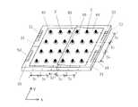
図1に示すように、点光源素子である発光ダイオード(LED)2は、支持基板3上に、平面状かつ規則的に配列され、液晶表示装置用バックライト1を構成している。図1(a)はバックライトの平面図であり、図1(b)は図1(a)の矢印X−X'における断面図を示している。 As shown in FIG. 1, light emitting diodes (LEDs) 2 that are point light source elements are regularly and regularly arranged on a
また、支持基板3上には、LEDの配置位置に開口40を形成した反射シート4が配置されている。これは、バックライトの前面に配置された液晶パネル方向に、LEDから出射する光を指向させる役割を担っている。 Further, on the
このようなバックライトは、特許文献1にも開示されているが、液晶表示装置の大画面化が進むに従い、バックライトを単一の支持基板で構成することは、製造コストの増大の原因となる。つまり、大画面に対応する単一の支持基板は、価格が高い上、取扱いが煩雑であり、支持基板の一部領域に欠陥が生じた場合でも基板全体を交換する必要があり、極めて高コストとなる。
このような問題を解消するため、図2に示すように、点光源素子2が配列される全領域Aを、複数の小領域a1〜a8に分割し、小領域毎に支持基板31〜38を設け、各支持基板上に点光源素子であるLED2を配置することが行われている。符号51〜58は各支持基板に配置されたLED2を駆動するための電力等を給電するためのコネクタである。なお、図2中の点線は、LED2が連続して配置される様子を省略して示していることを表示している。In order to solve such a problem, as shown in FIG. 2, the entire area A in which the point
このような、分割した支持基板は、比較的サイズの小さな支持基板が利用可能であり、バックライトの一部領域に欠陥が発生しても、該当する支持基板のみを交換することで、簡単に補修することができる。また、図2に示すように、全領域Aを、等分割した場合においては、各小領域a1〜a8に、同じサイズの支持基板で同じ数や配置のLEDを有する共通のバックライトユニットを利用することもでき、製造コストを大幅に低減することが可能である。Such a divided support substrate can be a relatively small support substrate, and even if a defect occurs in a part of the backlight, it is easy to replace only the corresponding support substrate. Can be repaired. In addition, as shown in FIG. 2, when the entire area A is equally divided, each of the small areas a1 to a8 has a common backlight unit having the same number and arrangement of LEDs on the same size of the support substrate. Can be used, and the manufacturing cost can be greatly reduced.
また、図1に示した反射シート4は、分割した支持基板に対しても同様に利用できる。 Moreover, the
しかしながら、反射シートと支持基板とは、通常、両面テープ又は接着剤等を利用して接合されているため、液晶表示装置の大画面化に伴い、反射シート4に形成されるLED用の開口40を、支持基板上に配置されたLED2に、精度良く位置合わせを行うことが困難となる。 However, since the reflection sheet and the support substrate are usually bonded using a double-sided tape or an adhesive, the LED opening 40 formed in the
更には、分割した支持基板を1枚の大きな反射シートで覆ってしまうため、仮に一つの支持基板を交換しようとした場合でも、反射シート全体を剥がす必要があり、支持基板を分割したメリットが低下してしまう。 Furthermore, since the divided support substrate is covered with one large reflection sheet, even if one support substrate is to be replaced, it is necessary to peel off the entire reflection sheet, and the merit of dividing the support substrate is reduced. Resulting in.
本発明が解決しようとする課題は、上述したような問題を解決し、点光源素子が配列される全領域が複数の小領域に分割され、各小領域毎に対応するバックライトユニットを設ける場合でも、作業性を向上することが出来、更には、輝度の均一化もできる液晶表示装置用バックライト及びそれを用いた液晶表示装置を提供することである。 The problem to be solved by the present invention is to solve the above-described problem, when the entire area where the point light source elements are arranged is divided into a plurality of small areas, and a corresponding backlight unit is provided for each small area However, an object of the present invention is to provide a backlight for a liquid crystal display device that can improve workability and can make the luminance uniform, and a liquid crystal display device using the same.
上記課題を解決するために、本発明は以下のような特徴を有している。 In order to solve the above problems, the present invention has the following features.
(1)複数の点光源素子を平面状に複数配列した液晶表示装置用バックライトにおいて、
点光源素子が配列される全領域が複数の小領域に分割され、小領域毎に、点光源素子を支持する支持基板と、該支持基板上に配置される点光源素子とから構成される複数のバックライトユニットと、
該バックライトユニットの該支持基板上に配置され、該点光源素子の配置位置に開口が形成された反射シートを有し、
該反射シートは該全領域を複数のシートで覆うように構成されていることを特徴とする。(1) In a backlight for a liquid crystal display device in which a plurality of point light source elements are arranged in a plane,
The entire region in which the point light source elements are arranged is divided into a plurality of small regions, and each of the small regions includes a plurality of support substrates that support the point light source elements and point light source elements that are arranged on the support substrate. Backlight unit,
A reflection sheet disposed on the support substrate of the backlight unit and having an opening formed at the position of the point light source element;
The reflective sheet is configured to cover the entire area with a plurality of sheets.
(2)上記(1)に記載の液晶表示装置用バックライトにおいて、該バックライトユニットを平面状に隣接配置した際に、該シート同士が隣接する境界を挟む点光源素子の配置間隔は、単一の反射シートの内部に配置される点光源素子の配置間隔よりも狭くなるように設定されていることを特徴とする。(2) In the backlight for a liquid crystal display device according to the above (1), when the backlight units are arranged adjacent to each other in a planar shape, the arrangement interval of the point light source elements sandwiching the boundary where the sheets are adjacent to each other is simply set. It is characterized in that it is set to be narrower than the arrangement interval of the point light source elements arranged inside one reflection sheet.
(3)上記(1)に記載の液晶表示装置用バックライトにおいて、該反射シートを構成する各シートは、少なくとも1つの小領域を含み、かつ小領域を最小単位とする面積を有することを特徴とする。(3) In the backlight for a liquid crystal display device according to (1), each sheet constituting the reflective sheet includes at least one small region and has an area with the small region as a minimum unit. And
(4)上記(3)に記載の液晶表示装置用のバックライトにおいて、該反射シートを構成する各シートは、各バックライトユニットとほぼ同じ面積を有することを特徴とする。(4) In the backlight for a liquid crystal display device according to (3), each sheet constituting the reflection sheet has substantially the same area as each backlight unit.
(5)上記(1)に記載の液晶表示装置用バックライトにおいて、該反射シートを構成する各シートは、互いに重なり合うように配置されていることを特徴とする。(5) In the backlight for a liquid crystal display device according to (1), the sheets constituting the reflective sheet are arranged so as to overlap each other.
(6)上記(1)に記載の液晶表示装置用バックライトにおいて、該点光源素子が発光ダイオードであることを特徴とする。(6) The backlight for a liquid crystal display device according to (1), wherein the point light source element is a light emitting diode.
(7)液晶表示パネルと、該液晶表示パネルに光を照射する直下型のバックライトを備えた液晶表示装置において、
該バックライトは、上記(1)乃至(6)のいずれかに記載の液晶表示装置用バックライトを用いることを特徴とする。(7) In a liquid crystal display device comprising a liquid crystal display panel and a direct type backlight for irradiating the liquid crystal display panel with light,
As the backlight, the backlight for a liquid crystal display device according to any one of the above (1) to (6) is used.
本発明により、点光源素子が配列される全領域が複数の小領域に分割され、小領域毎に対応するバックライトユニットを利用する場合でも、該全領域を覆う反射シートを複数のシートで形成することで、組み立てや交換などの作業性を向上することが出来る。更には、該シート同士の境界での輝度の低下を、点光源素子の配置間隔で調整することが可能となる。このため、画面の縦方向または横方向に発生する輝度の落ち込みを抑制し、高品質な画像を提供できる。 According to the present invention, the entire region in which the point light source elements are arranged is divided into a plurality of small regions, and even when a backlight unit corresponding to each small region is used, a reflective sheet covering the entire region is formed with a plurality of sheets. By doing so, workability such as assembly and replacement can be improved. Furthermore, it is possible to adjust the decrease in luminance at the boundary between the sheets by the arrangement interval of the point light source elements. For this reason, it is possible to suppress a drop in luminance occurring in the vertical or horizontal direction of the screen and provide a high-quality image.
しかも、反射シートを構成する各シートを、少なくとも1つの小領域を含み、かつ小領域を最小単位とする面積を有するよう調整するか、さらには、各バックライトユニットとほぼ同じ面積を有するように調整することにより、隣接配置されるバックライトユニット同士の境界に近い点光源素子の配置を調整するだけで、容易に輝度の落ち込みを調整することができる。しかも、輝度の落ち込みがバックライトユニット同士の境界のみで発生するため、同一規格(支持基板の大きさや点光源素子の数や配置が同じ)のバックライトユニットであっても、輝度の落ち込みを抑制することが可能となる。 In addition, each sheet constituting the reflection sheet is adjusted to have an area including at least one small region and having the small region as a minimum unit, or to have substantially the same area as each backlight unit. By adjusting, it is possible to easily adjust the drop in luminance simply by adjusting the arrangement of the point light source elements close to the boundary between the adjacent backlight units. Moreover, since the brightness drop occurs only at the boundary between the backlight units, the brightness drop is suppressed even for backlight units of the same standard (the size of the support substrate and the number and arrangement of point light source elements are the same). It becomes possible to do.
以下、本発明の構成について、好適例を用いて詳細に説明する。 Hereinafter, the configuration of the present invention will be described in detail using preferred examples.
図7は、本発明が適用される液晶表示装置の概略構成図である。液晶表示パネルPNLは観察者側に配置され、該液晶表示パネルPNLの後方にシートOS、及びバックライトBLが順次配置されている。 FIG. 7 is a schematic configuration diagram of a liquid crystal display device to which the present invention is applied. The liquid crystal display panel PNL is disposed on the viewer side, and a sheet OS and a backlight BL are sequentially disposed behind the liquid crystal display panel PNL.
液晶表示パネルPNLは、一対の平行配置された、例えば、ガラスからなる基板SUB1、SUB2を有し、これら各基板SUB1、SUB2の間に液晶が挟持される。基板SUB1、SUB2の液晶側の面には、マトリックス状に配置された画素(図示せず)が該液晶を一構成要素として形成され、これら画素毎にその光透過率を制御できる。これら各画素が形成された領域を表示領域AR(図中一点鎖線枠で囲まれた領域)とし、この表示領域ARにおいて、バックライトBLからの光を通して観察者に画像を認識させる。 The liquid crystal display panel PNL includes a pair of parallel substrates SUB1 and SUB2 made of glass, for example, and liquid crystal is sandwiched between the substrates SUB1 and SUB2. Pixels (not shown) arranged in a matrix are formed on the surface of the substrates SUB1 and SUB2 on the liquid crystal side as a constituent element, and the light transmittance of each pixel can be controlled. The area where these pixels are formed is defined as a display area AR (area surrounded by a one-dot chain line in the figure), and the viewer recognizes an image through light from the backlight BL in the display area AR.
基板SUB1は、例えば、図中左側辺及び上側辺において基板SUB2から露出された部分を有し、これらの部分において、複数のフレキシブル基板FBの一辺側が接続されている。これらフレキシブル基板FBには、前記各画素を独立に駆動させるための映像信号駆動回路He及び走査信号駆動回路Vが形成されている。 The substrate SUB1 has, for example, portions exposed from the substrate SUB2 on the left side and the upper side in the drawing, and one side of the plurality of flexible substrates FB is connected to these portions. The flexible substrate FB is formed with a video signal driving circuit He and a scanning signal driving circuit V for independently driving the pixels.
図中x方向に並設されるフレキシブル基板FBには、映像信号駆動回路Heが形成される。この映像信号駆動回路Heが形成されたフレキシブル基板FBは、基板SUB1と接続された一辺側と対向する他の辺側にプリント基板PCB1、PCB2が接続され、プリント基板PCB1、PCB2を介して図示しない制御回路から映像信号が入力される。また、図中y方向に並設されるフレキシブル基板FBには、走査信号駆動回路Vが形成される。この走査信号駆動回路Vが形成されたフレキシブル基板FBは、表示制御回路(図示せず)からの入力信号がプリント基板PCB1と基板SUB1の表面に形成された配線(図示せず)を介して入力されるようになっており、前記映像信号駆動回路Heが載置されたフレキシブル基板FBのように、プリント基板PCB1、PCB2に相当する他の基板は、特に、接続されていない。 A video signal drive circuit He is formed on the flexible substrate FB arranged in parallel in the x direction in the drawing. The flexible substrate FB on which the video signal driving circuit He is formed has printed circuit boards PCB1 and PCB2 connected to the other side opposite to the one side connected to the substrate SUB1, and is not shown through the printed circuit boards PCB1 and PCB2. A video signal is input from the control circuit. A scanning signal drive circuit V is formed on the flexible substrate FB arranged in parallel in the y direction in the drawing. In the flexible substrate FB on which the scanning signal drive circuit V is formed, an input signal from a display control circuit (not shown) is input via wiring (not shown) formed on the surface of the printed circuit board PCB1 and the substrate SUB1. Other substrates corresponding to the printed circuit boards PCB1 and PCB2 are not particularly connected like the flexible circuit board FB on which the video signal driving circuit He is mounted.
液晶表示パネルPNLの背面には、例えば、拡散シート、プリズムシート、あるいはこれらの積層体からなる光学シートOSを介してバックライトBLが配置されている。光学シートOSは、バックライトBLからの光を拡散、あるいは集光させたりして液晶表示パネルPNLに導くようになっている。 On the back surface of the liquid crystal display panel PNL, for example, a backlight BL is disposed via an optical sheet OS made of a diffusion sheet, a prism sheet, or a laminate thereof. The optical sheet OS guides the light from the backlight BL to the liquid crystal display panel PNL by diffusing or condensing it.
バックライトBLは、液晶表示パネルPNLの少なくとも表示領域ARと対向して配置される支持基板3の表面に、複数のLED2がマトリックス状に配置されることによって形成されている。 The backlight BL is formed by arranging a plurality of
本発明のバックライトBLにおける支持基板は、図2に示されるように、複数の小領域a1〜a8に分割されている。本発明では、更に、反射シートも複数の小領域に分割される。(後述する図5参照)
反射シートが複数に分割されていることにより、支持基板の着脱が容易になり、作業性が向上する。As shown in FIG. 2, the support substrate in the backlight BL of the present invention is divided into a plurality of small regions a1 to a8 . In the present invention, the reflection sheet is further divided into a plurality of small regions. (Refer to FIG. 5 described later)
Since the reflection sheet is divided into a plurality of parts, the support substrate can be easily attached and detached, and workability is improved.
しかしながら、反射シートを小領域毎に分割することは、図3に示すように、点光源素子が形成するバックライトの輝度分布にムラを生じることとなる。
図3のa1〜a8は、図2に示す小領域a1〜a8に対応する領域であり、各小領域の支持基板上には、支持基板とほぼ同じ大きさを有する反射シートが配置されている。However, dividing the reflection sheet into small areas causes unevenness in the luminance distribution of the backlight formed by the point light source elements, as shown in FIG.
A1 ~a8 in FIG. 3 is a region corresponding to the small region a1 ~a8 shown in FIG. 2, each small region of the support substrate, a reflection sheet having approximately the same size as the supporting substrate Has been placed.
本発明者らは、図3の構造において、小領域毎に64個のLEDを配置し、バックライト全領域においてLEDを26mm程度の等間隔で配置すると共に、支持基板から約17mm程度上方における輝度分布を測定した。 In the structure of FIG. 3, the present inventors arrange 64 LEDs for each small area, arrange LEDs at an equal interval of about 26 mm in the entire backlight area, and brightness about 17 mm above the support substrate. Distribution was measured.
図3には測定した輝度分布の概略を追記している。バックライト中央横方向(x軸方向)の輝度分布はグラフc1に、バックライト中央縦方向(y軸方向)の輝度分布はグラフc2に示すような形状の分布となる。このように、小領域の境界部分では、輝度Eの落込みb1〜b4が見られ、特に、落ち込みb1では、周辺の輝度と比較し4%程度の減少が見られた。FIG. 3 shows an outline of the measured luminance distribution. Luminance distribution of the backlight central lateral (x-axis direction) in the graph c1, the luminance distribution of the backlight central longitudinal direction (y-axis direction) is the distribution of the shape as shown in the graph c2. In this way, the luminance b drops b1 to b4 were observed at the boundary portion of the small region, and in particular, at the
上述したような輝度の落ち込みは、液晶表示装置に縦線又は横線の影を形成し、画質の低下の原因となる、特に、図3が示すように、横方向(x方向)の輝度の落ち込みb1は、周辺が連続して高輝度を維持している分、視覚者には輝度の低下が顕著に認識されるという問題がある。 The drop in luminance as described above causes a shadow of a vertical line or a horizontal line on the liquid crystal display device and causes deterioration in image quality. In particular, as shown in FIG. 3, the drop in luminance in the horizontal direction (x direction). The problem of b1 is that a decrease in luminance is noticeably perceived by the viewer because the periphery continuously maintains high luminance.
そのため、本発明では更に、隣接する支持基板間のLED2の配置間隔を他の位置の配置間隔よりも狭くした。具体例は、図4に示す。図4は、小領域(a1,a2)の拡大断面図であり、LED2複数配置した支持基板31,32上に、該LED2の配置位置に開口40が形成された反射シート41,42が貼り付けられている。各支持基板上のLED2の配置間隔はS1で示され、隣接する支持基板間のLED2の間隔はS2で示される。Therefore, in the present invention, the arrangement interval of the
図4で示されるように、LED2の配置間隔は、S1>S2となるように設定されている。As shown in FIG. 4, the arrangement interval of the LEDs2 is set so that S1 > S2 .
本実施例の構成では、輝度分布の落ち込みが発生する支持基板の境界部分では、LED2の配置間隔が、他の領域よりも狭くなっているため、輝度の低下を抑制でき、全体として輝度分布の落ち込みが少ないバックライトを形成することが可能となる。 In the configuration of this embodiment, the
例えば、図3で示した、LEDを26mm程度のピッチ間隔で配置する場合では、反射シート同士の境界を挟む点光源素子の配置間隔を23mm程度とすることで、輝度を4%程度上昇させることができる。 For example, in the case where the LEDs are arranged at a pitch interval of about 26 mm as shown in FIG. 3, the luminance is increased by about 4% by setting the arrangement interval of the point light source elements sandwiching the boundary between the reflection sheets to about 23 mm. Can do.
更に本発明では、図5及び図6が示すように、支持基板31,32(バックライトユニット)の境界部分において、反射シート43,44が重複するよう設定している。これにより、支持基板間の境界と反射シート間の境界をずらすことが出来、支持基板間の輝度分布の落ち込みを更に低減することが可能となる。 Furthermore, in this invention, as FIG.5 and FIG.6 shows, it sets so that the
本発明では、「バックライトユニット」は、一つの支持基板に点光源素子が配置されているものを意味しており、支持基板が複数配列されて全体として「バックライト」を構成しているように、「バックライトユニット」が複数配列されて「バックライト」本体を構成している。 In the present invention, the “backlight unit” means that a point light source element is arranged on one support substrate, and a plurality of support substrates are arranged to constitute a “backlight” as a whole. In addition, a plurality of “backlight units” are arranged to constitute a “backlight” body.
図5は、2つの支持基板(バックライトユニット)(31と33又は32と34)を1つの反射シート(43又は44)で覆っている例である。ここで示すように、反射シートは、支持基板毎に1枚ずつ配置するばかりでなく、複数の支持基板に対して1枚の反射シートを配置しても良い。反射シートを構成する各シートは、少なくとも1つの小領域(バックライトユニット)を含み、かつ小領域を最小単位とする面積を有していればよい。 FIG. 5 shows an example in which two support substrates (backlight units) (31 and 33 or 32 and 34) are covered with one reflection sheet (43 or 44). As shown here, not only one reflection sheet is provided for each support substrate, but also one reflection sheet may be provided for a plurality of support substrates. Each sheet constituting the reflection sheet may include at least one small area (backlight unit) and have an area having the small area as a minimum unit.
ここでは、「少なくとも1の小領域を含む面積」であることと、「小領域を最小単位とする面積」であることが必要である。特に、「小領域を最小単位とする面積」とは、図5に示すように、支持基板31を覆う反射シート43が他の支持基板33も覆う場合は、支持基板33の反射シートが必要な領域のすべてを覆うように構成されており、例えば、支持基板33の反射シートが必要な領域の一部のみを覆うものではないことを意図している。 Here, it is necessary to be “an area including at least one small region” and “an area having a small region as a minimum unit”. In particular, the “area having a small region as a minimum unit” means that when the
図5が示すように、反射シート43及び44の境界部分は、支持基板31と32との間又は支持基板33と34との間に位置しており、支持基板31と32との境界を挟むLED2の配置間隔S2を、同じ方向の他の配置間隔S1より狭くするよう支持基板上の点光源素子の位置が調整されている。ただし、支持基板31と33との間や支持基板32と34との間では、反射シート同士の境界が存在しないため、同じ方向の他のLED2の配置間隔と同じ間隔S3に設定されている。As shown in FIG. 5, the boundary between the
図6は、1つの支持基板(バックライトユニット)31毎に、反射シート41を設けるものであり、該反射シートを構成する各シートは、各バックライトユニットとほぼ同じ面積を有している。 In FIG. 6, a
図5又は図6のように、支持基板(バックライトユニット)同士の境界部分に反射シート同士の境界を位置付けることにより、点光源素子の配置間隔の調整が必要な部分を、支持基板の側部近傍の点光源素子のみとするように、支持基板上で常に同じ位置に設定できる。そして、このような構成を採用することで、同一規格(支持基板の大きさや点光源素子の数や配置が同じ)のバックライトユニットであっても、輝度の落ち込みを簡単に抑制することが可能となる。 As shown in FIG. 5 or FIG. 6, by positioning the boundary between the reflection sheets at the boundary between the support substrates (backlight units), the portion that needs to be adjusted in the arrangement interval of the point light source elements is arranged on the side of the support substrate. It can always be set at the same position on the support substrate so that only the nearby point light source elements are used. By adopting such a configuration, it is possible to easily suppress a drop in luminance even for backlight units of the same standard (the size of the support substrate and the number and arrangement of point light source elements are the same). It becomes.
また、本発明の液晶表示装置用バックライトにおいて、図4又は図5に示すように、反射シートを構成する各シートは、互いに重なり合うように配置している。このような場合には、特に、輝度分布の落ち込みが発生し易くなるため、本発明を適用することが好ましい。 Further, in the backlight for a liquid crystal display device of the present invention, as shown in FIG. 4 or FIG. 5, the sheets constituting the reflective sheet are arranged so as to overlap each other. In such a case, it is particularly preferable to apply the present invention because a drop in luminance distribution is likely to occur.
以上の説明では、本発明の液晶表示装置用バックライトにおいて、点光源素子として発光ダイオード(LED)を中心に説明したが、本発明はLEDに限らず点状の光源であれば同様に適用可能であることは、言うまでもない。 In the above description, in the backlight for the liquid crystal display device of the present invention, the light emitting diode (LED) is mainly described as the point light source element. However, the present invention is not limited to the LED and can be similarly applied to any point light source. It goes without saying that.
以上説明したように、本発明によれば、点光源素子が配列される全領域が複数の小領域に分割され、各小領域毎に対応するバックライトユニットを設ける場合でも、画面の縦方向または横方向に発生する輝度の落ち込みを抑制し、高品質な画像を提供することが可能な、液晶表示装置用バックライト及びそれを用いる液晶表示装置を提供することができる。 As described above, according to the present invention, the entire area in which the point light source elements are arranged is divided into a plurality of small areas, and even when a backlight unit corresponding to each small area is provided, It is possible to provide a backlight for a liquid crystal display device and a liquid crystal display device using the same that can suppress a drop in luminance occurring in the horizontal direction and can provide a high-quality image.
1 バックライト
2 点光源素子
3,31〜38 支持基板
4,41〜44 反射シート
40 開口
51〜58 コネクタ
PNL 液晶表示パネル
OS 光学シート
BL バックライト
FB フレキシブル基板
He 映像信号駆動回路
V 走査信号駆動回路
SUB1,SUB2 基板
PCB1,PCB2 プリント基板
AR 表示領域DESCRIPTION OF
Claims (4)
Translated fromJapanese点光源素子が配列される全領域が連続した複数の小領域に分割され、小領域毎に、点光源素子を支持する支持基板と、該支持基板上に配置される点光源素子とから構成される複数のバックライトユニットと、
該バックライトユニットの該支持基板上に配置され、該点光源素子の配置位置に開口が形成された反射シートを有し、
該反射シートは該全領域を複数のシートで覆うように構成され、
該反射シートを構成する少なくとも1つのシートは、連続した2以上の該小領域上に配置され、
該バックライトユニットを平面状に隣接配置した際に、該シート同士が隣接する境界を挟む点光源素子の配置間隔は、単一のシートの内部に配置される点光源素子の配置間隔よりも狭くなるように設定されていること
を特徴とする液晶表示装置用バックライト。In a backlight for a liquid crystal display device in which a plurality of point light source elements are arranged in a plane,
The entire area where the point light source elements are arranged is divided into a plurality of continuous small areas, and each small area is composed of a support substrate for supporting the point light source elements and a point light source element disposed on the support substrate. A plurality of backlight units,
A reflection sheet disposed on the support substrate of the backlight unit and having an opening formed at the position of the point light source element;
The reflective sheet is configured to cover the entire area with a plurality of sheets,
At least one sheet constituting the reflective sheet is disposed on the two or more continuous small areas,
When the backlight units are arranged adjacent to each other in a planar shape, the arrangement interval of the point light source elements sandwiching the boundary between the sheets is narrower than the arrangement interval of the point light source elements arranged inside a single sheet. A backlight for a liquid crystal display device, wherein the backlightis set to be
該バックライトは、請求項1乃至3のいずれかに記載の液晶表示装置用バックライトを用いることを特徴とする液晶表示装置。In a liquid crystal display device comprising a liquid crystal display panel and a direct backlight for irradiating the liquid crystal display panel with light,
The backlight liquid crystal display device which comprises using a backlight for a liquid crystal display device according to any one of claims 1 to3.
Priority Applications (5)
| Application Number | Priority Date | Filing Date | Title |
|---|---|---|---|
| JP2008220135AJP5368751B2 (en) | 2008-08-28 | 2008-08-28 | Backlight for liquid crystal display device and liquid crystal display device using the same |
| TW098128386ATWI428670B (en) | 2008-08-28 | 2009-08-24 | A liquid crystal display device for backlighting and a liquid crystal display device using the same |
| US12/547,686US8243232B2 (en) | 2008-08-28 | 2009-08-26 | Backlight for liquid crystal display device and liquid crystal display device using the same |
| KR1020090079661AKR101095764B1 (en) | 2008-08-28 | 2009-08-27 | Backlight for liquid crystal display and liquid crystal display using the same |
| CN2009101710295ACN101661192B (en) | 2008-08-28 | 2009-08-28 | Backlight for liquid crystal display device and liquid crystal display device using the same |
Applications Claiming Priority (1)
| Application Number | Priority Date | Filing Date | Title |
|---|---|---|---|
| JP2008220135AJP5368751B2 (en) | 2008-08-28 | 2008-08-28 | Backlight for liquid crystal display device and liquid crystal display device using the same |
Publications (2)
| Publication Number | Publication Date |
|---|---|
| JP2010055952A JP2010055952A (en) | 2010-03-11 |
| JP5368751B2true JP5368751B2 (en) | 2013-12-18 |
Family
ID=41724907
Family Applications (1)
| Application Number | Title | Priority Date | Filing Date |
|---|---|---|---|
| JP2008220135AActiveJP5368751B2 (en) | 2008-08-28 | 2008-08-28 | Backlight for liquid crystal display device and liquid crystal display device using the same |
Country Status (5)
| Country | Link |
|---|---|
| US (1) | US8243232B2 (en) |
| JP (1) | JP5368751B2 (en) |
| KR (1) | KR101095764B1 (en) |
| CN (1) | CN101661192B (en) |
| TW (1) | TWI428670B (en) |
Families Citing this family (16)
| Publication number | Priority date | Publication date | Assignee | Title |
|---|---|---|---|---|
| WO2011013419A1 (en)* | 2009-07-31 | 2011-02-03 | シャープ株式会社 | Backlight device, displaying device, and television receiver |
| KR101628228B1 (en)* | 2009-09-10 | 2016-06-09 | 삼성디스플레이 주식회사 | Backlight assembly and display device comprising the same |
| WO2011048835A1 (en)* | 2009-10-19 | 2011-04-28 | シャープ株式会社 | Lighting device and display device |
| CN102563447A (en)* | 2010-12-30 | 2012-07-11 | 苏州世鼎电子有限公司 | LED (light-emitting diode) backlight module with high process yield and manufacturing method thereof |
| US20140321156A1 (en)* | 2011-11-11 | 2014-10-30 | Sharp Kabushiki Kaisha | Backlight device |
| US20160004123A1 (en)* | 2014-07-02 | 2016-01-07 | Kabushiki Kaisha Toshiba | Image display apparatus |
| US9995962B2 (en)* | 2015-06-12 | 2018-06-12 | Samsung Display Co., Ltd. | Backlight unit and display apparatus including the same |
| WO2017150035A1 (en)* | 2016-03-01 | 2017-09-08 | ソニー株式会社 | Light emitting device, display apparatus, and illumination apparatus |
| CN109946873A (en)* | 2017-12-20 | 2019-06-28 | 鸿富锦精密工业(深圳)有限公司 | Backlight Module |
| KR102448600B1 (en)* | 2018-02-26 | 2022-09-28 | 엘지전자 주식회사 | display device |
| CN110297356A (en)* | 2019-06-25 | 2019-10-01 | 厦门天马微电子有限公司 | A kind of lamp plate, backlight module and curved-surface display device |
| JP2021157875A (en) | 2020-03-25 | 2021-10-07 | 株式会社ジャパンディスプレイ | Illuminating device and display device |
| WO2022215830A1 (en)* | 2021-04-08 | 2022-10-13 | 엘지전자 주식회사 | Display device |
| CN113448123A (en)* | 2021-06-21 | 2021-09-28 | Tcl华星光电技术有限公司 | Backlight module and display device |
| CN114170919A (en)* | 2021-12-13 | 2022-03-11 | Tcl华星光电技术有限公司 | Double-sided display panel and double-sided display splicing screen |
| WO2025065777A1 (en)* | 2023-09-27 | 2025-04-03 | 瑞仪(广州)光电子器件有限公司 | Reflective structure with overlapping areas overlapping with each other, backlight module and display device |
Family Cites Families (8)
| Publication number | Priority date | Publication date | Assignee | Title |
|---|---|---|---|---|
| JP4543813B2 (en) | 2004-08-04 | 2010-09-15 | ソニー株式会社 | Backlight device and liquid crystal display device including the backlight device |
| KR100609057B1 (en)* | 2004-11-17 | 2006-08-09 | 삼성전자주식회사 | Backlight Unit |
| KR101134302B1 (en)* | 2005-06-30 | 2012-04-13 | 엘지디스플레이 주식회사 | cover bottom for liquid crystal display device, LED back light assembly and liquid crystal display module using thereof |
| KR100645788B1 (en) | 2005-08-26 | 2006-11-14 | 주식회사 파이컴 | Backlit device |
| JP2007073295A (en) | 2005-09-06 | 2007-03-22 | Sharp Corp | Direct backlight device and image display device |
| KR101237788B1 (en)* | 2005-12-29 | 2013-02-28 | 엘지디스플레이 주식회사 | LED light emitting unit and LED backlight assembly and liquid crystal display module |
| JP4857945B2 (en)* | 2006-06-21 | 2012-01-18 | ソニー株式会社 | Planar light source device and liquid crystal display device assembly |
| KR20080013592A (en)* | 2006-08-09 | 2008-02-13 | 삼성전자주식회사 | Backlight unit and display device including same |
- 2008
- 2008-08-28JPJP2008220135Apatent/JP5368751B2/enactiveActive
- 2009
- 2009-08-24TWTW098128386Apatent/TWI428670B/enactive
- 2009-08-26USUS12/547,686patent/US8243232B2/enactiveActive
- 2009-08-27KRKR1020090079661Apatent/KR101095764B1/enactiveActive
- 2009-08-28CNCN2009101710295Apatent/CN101661192B/enactiveActive
Also Published As
| Publication number | Publication date |
|---|---|
| US8243232B2 (en) | 2012-08-14 |
| CN101661192B (en) | 2011-12-14 |
| KR20100027023A (en) | 2010-03-10 |
| TW201027188A (en) | 2010-07-16 |
| KR101095764B1 (en) | 2011-12-21 |
| CN101661192A (en) | 2010-03-03 |
| JP2010055952A (en) | 2010-03-11 |
| US20100053505A1 (en) | 2010-03-04 |
| TWI428670B (en) | 2014-03-01 |
Similar Documents
| Publication | Publication Date | Title |
|---|---|---|
| JP5368751B2 (en) | Backlight for liquid crystal display device and liquid crystal display device using the same | |
| US7481553B2 (en) | Backlight assembly and liquid crystal display module using the same | |
| KR101255833B1 (en) | Liquid crystal display device | |
| KR101294749B1 (en) | Liquid crystal display device | |
| KR101594616B1 (en) | Backlight unit and liquid crystal display device having the same | |
| US20100165232A1 (en) | Liquid crystal display device | |
| CN106959534B (en) | Display device | |
| US20100283718A1 (en) | Light-emitting unit and backlight apparatus having the same | |
| KR102296788B1 (en) | Liquid crystal display device | |
| CN100435003C (en) | Backlight unit and liquid crystal display with the backlight unit | |
| KR20130021201A (en) | Liquid crystal display device | |
| US20110211139A1 (en) | Display device | |
| JP2013239289A (en) | Planar light source apparatus, and display apparatus equipped with the same | |
| US9116277B2 (en) | Lighting device, display device, and television receiver | |
| KR20110071725A (en) | LCD Display Module | |
| JP5414250B2 (en) | Liquid crystal display | |
| US20060256579A1 (en) | Backlight structure and lighting module therefor | |
| KR101261881B1 (en) | Light Emitting Diode assembly and liquid crystal display module with the same | |
| US20150103258A1 (en) | Lighting device, display device and television device | |
| CN116381979A (en) | Display device | |
| JP2010232050A (en) | Liquid crystal display | |
| KR20130074553A (en) | Flexible printed circuit of liquid crystal display device | |
| JP2010277853A (en) | Backlight | |
| KR20110024270A (en) | Backlight unit and liquid crystal display device having same | |
| WO2010113349A1 (en) | Led illuminating device, and display device provided with the led illuminating device |
Legal Events
| Date | Code | Title | Description |
|---|---|---|---|
| A621 | Written request for application examination | Free format text:JAPANESE INTERMEDIATE CODE: A621 Effective date:20101116 | |
| A711 | Notification of change in applicant | Free format text:JAPANESE INTERMEDIATE CODE: A712 Effective date:20110216 | |
| RD03 | Notification of appointment of power of attorney | Free format text:JAPANESE INTERMEDIATE CODE: A7423 Effective date:20110216 | |
| A977 | Report on retrieval | Free format text:JAPANESE INTERMEDIATE CODE: A971007 Effective date:20120319 | |
| RD02 | Notification of acceptance of power of attorney | Free format text:JAPANESE INTERMEDIATE CODE: A7422 Effective date:20120330 | |
| A131 | Notification of reasons for refusal | Free format text:JAPANESE INTERMEDIATE CODE: A131 Effective date:20120427 | |
| RD04 | Notification of resignation of power of attorney | Free format text:JAPANESE INTERMEDIATE CODE: A7424 Effective date:20120530 | |
| RD04 | Notification of resignation of power of attorney | Free format text:JAPANESE INTERMEDIATE CODE: A7424 Effective date:20120530 | |
| A521 | Request for written amendment filed | Free format text:JAPANESE INTERMEDIATE CODE: A523 Effective date:20120625 | |
| A02 | Decision of refusal | Free format text:JAPANESE INTERMEDIATE CODE: A02 Effective date:20120807 | |
| A521 | Request for written amendment filed | Free format text:JAPANESE INTERMEDIATE CODE: A523 Effective date:20121010 | |
| A911 | Transfer to examiner for re-examination before appeal (zenchi) | Free format text:JAPANESE INTERMEDIATE CODE: A911 Effective date:20121017 | |
| A912 | Re-examination (zenchi) completed and case transferred to appeal board | Free format text:JAPANESE INTERMEDIATE CODE: A912 Effective date:20130111 | |
| A521 | Request for written amendment filed | Free format text:JAPANESE INTERMEDIATE CODE: A523 Effective date:20130702 | |
| A61 | First payment of annual fees (during grant procedure) | Free format text:JAPANESE INTERMEDIATE CODE: A61 Effective date:20130913 | |
| R150 | Certificate of patent or registration of utility model | Ref document number:5368751 Country of ref document:JP Free format text:JAPANESE INTERMEDIATE CODE: R150 Free format text:JAPANESE INTERMEDIATE CODE: R150 | |
| R250 | Receipt of annual fees | Free format text:JAPANESE INTERMEDIATE CODE: R250 | |
| R250 | Receipt of annual fees | Free format text:JAPANESE INTERMEDIATE CODE: R250 | |
| R250 | Receipt of annual fees | Free format text:JAPANESE INTERMEDIATE CODE: R250 | |
| R250 | Receipt of annual fees | Free format text:JAPANESE INTERMEDIATE CODE: R250 | |
| R250 | Receipt of annual fees | Free format text:JAPANESE INTERMEDIATE CODE: R250 | |
| R250 | Receipt of annual fees | Free format text:JAPANESE INTERMEDIATE CODE: R250 | |
| R250 | Receipt of annual fees | Free format text:JAPANESE INTERMEDIATE CODE: R250 | |
| S111 | Request for change of ownership or part of ownership | Free format text:JAPANESE INTERMEDIATE CODE: R313117 | |
| R250 | Receipt of annual fees | Free format text:JAPANESE INTERMEDIATE CODE: R250 | |
| R350 | Written notification of registration of transfer | Free format text:JAPANESE INTERMEDIATE CODE: R350 | |
| R250 | Receipt of annual fees | Free format text:JAPANESE INTERMEDIATE CODE: R250 | |
| S111 | Request for change of ownership or part of ownership | Free format text:JAPANESE INTERMEDIATE CODE: R313117 | |
| R350 | Written notification of registration of transfer | Free format text:JAPANESE INTERMEDIATE CODE: R350 | |
| R250 | Receipt of annual fees | Free format text:JAPANESE INTERMEDIATE CODE: R250 |