JP5366517B2 - Method for manufacturing semiconductor device - Google Patents
Method for manufacturing semiconductor deviceDownload PDFInfo
- Publication number
- JP5366517B2 JP5366517B2JP2008303618AJP2008303618AJP5366517B2JP 5366517 B2JP5366517 B2JP 5366517B2JP 2008303618 AJP2008303618 AJP 2008303618AJP 2008303618 AJP2008303618 AJP 2008303618AJP 5366517 B2JP5366517 B2JP 5366517B2
- Authority
- JP
- Japan
- Prior art keywords
- layer
- single crystal
- substrate
- inorganic insulating
- insulating film
- Prior art date
- Legal status (The legal status is an assumption and is not a legal conclusion. Google has not performed a legal analysis and makes no representation as to the accuracy of the status listed.)
- Expired - Fee Related
Links
- 239000004065semiconductorSubstances0.000titleclaimsabstractdescription894
- 238000000034methodMethods0.000titleclaimsdescription187
- 238000004519manufacturing processMethods0.000titleclaimsdescription143
- 239000000758substrateSubstances0.000claimsabstractdescription444
- 238000000926separation methodMethods0.000claimsabstractdescription66
- 229920005989resinPolymers0.000claimsdescription43
- 239000011347resinSubstances0.000claimsdescription43
- 238000009832plasma treatmentMethods0.000claimsdescription39
- 238000004544sputter depositionMethods0.000claimsdescription27
- 230000002441reversible effectEffects0.000claimsdescription10
- 230000000149penetrating effectEffects0.000claimsdescription9
- 238000010030laminatingMethods0.000claims2
- 239000013078crystalSubstances0.000abstractdescription435
- 230000015572biosynthetic processEffects0.000abstractdescription57
- 230000002829reductive effectEffects0.000abstractdescription29
- 230000010354integrationEffects0.000abstractdescription14
- 239000010410layerSubstances0.000description1062
- 239000010408filmSubstances0.000description413
- 239000012535impuritySubstances0.000description83
- VYPSYNLAJGMNEJ-UHFFFAOYSA-NSilicium dioxideChemical compoundO=[Si]=OVYPSYNLAJGMNEJ-UHFFFAOYSA-N0.000description64
- 150000002500ionsChemical class0.000description62
- 229910052814silicon oxideInorganic materials0.000description61
- 230000008569processEffects0.000description59
- 239000007789gasSubstances0.000description56
- 238000010438heat treatmentMethods0.000description48
- 238000005530etchingMethods0.000description47
- 229910052710siliconInorganic materials0.000description45
- XUIMIQQOPSSXEZ-UHFFFAOYSA-NSiliconChemical compound[Si]XUIMIQQOPSSXEZ-UHFFFAOYSA-N0.000description41
- 239000010703siliconSubstances0.000description41
- 229910052581Si3N4Inorganic materials0.000description40
- HQVNEWCFYHHQES-UHFFFAOYSA-Nsilicon nitrideChemical compoundN12[Si]34N5[Si]62N3[Si]51N64HQVNEWCFYHHQES-UHFFFAOYSA-N0.000description40
- 239000010409thin filmSubstances0.000description40
- 239000001257hydrogenSubstances0.000description39
- 229910052739hydrogenInorganic materials0.000description39
- 238000011282treatmentMethods0.000description39
- 239000000463materialSubstances0.000description38
- IJGRMHOSHXDMSA-UHFFFAOYSA-NAtomic nitrogenChemical compoundN#NIJGRMHOSHXDMSA-UHFFFAOYSA-N0.000description37
- -1halogen ionChemical class0.000description35
- 230000006870functionEffects0.000description32
- 229910052721tungstenInorganic materials0.000description32
- 239000010937tungstenSubstances0.000description29
- 238000012545processingMethods0.000description27
- 239000001301oxygenSubstances0.000description25
- 229910052760oxygenInorganic materials0.000description25
- 239000011241protective layerSubstances0.000description25
- UFHFLCQGNIYNRP-UHFFFAOYSA-NHydrogenChemical compound[H][H]UFHFLCQGNIYNRP-UHFFFAOYSA-N0.000description24
- WFKWXMTUELFFGS-UHFFFAOYSA-NtungstenChemical compound[W]WFKWXMTUELFFGS-UHFFFAOYSA-N0.000description24
- 238000005498polishingMethods0.000description22
- 239000010936titaniumSubstances0.000description22
- QVGXLLKOCUKJST-UHFFFAOYSA-Natomic oxygenChemical compound[O]QVGXLLKOCUKJST-UHFFFAOYSA-N0.000description21
- 238000005229chemical vapour depositionMethods0.000description21
- 230000001070adhesive effectEffects0.000description20
- 239000000126substanceSubstances0.000description20
- 230000007547defectEffects0.000description19
- 229910052757nitrogenInorganic materials0.000description18
- ZOKXTWBITQBERF-UHFFFAOYSA-NMolybdenumChemical compound[Mo]ZOKXTWBITQBERF-UHFFFAOYSA-N0.000description16
- 239000000853adhesiveSubstances0.000description16
- 239000011733molybdenumSubstances0.000description16
- PXHVJJICTQNCMI-UHFFFAOYSA-NNickelChemical compound[Ni]PXHVJJICTQNCMI-UHFFFAOYSA-N0.000description15
- KDLHZDBZIXYQEI-UHFFFAOYSA-NPalladiumChemical compound[Pd]KDLHZDBZIXYQEI-UHFFFAOYSA-N0.000description15
- BLRPTPMANUNPDV-UHFFFAOYSA-NSilaneChemical compound[SiH4]BLRPTPMANUNPDV-UHFFFAOYSA-N0.000description15
- 229910052750molybdenumInorganic materials0.000description15
- 235000012431wafersNutrition0.000description15
- GQPLMRYTRLFLPF-UHFFFAOYSA-NNitrous OxideChemical compound[O-][N+]#NGQPLMRYTRLFLPF-UHFFFAOYSA-N0.000description14
- 229910052782aluminiumInorganic materials0.000description14
- 239000012298atmosphereSubstances0.000description14
- 239000012790adhesive layerSubstances0.000description13
- 239000000956alloySubstances0.000description13
- XAGFODPZIPBFFR-UHFFFAOYSA-NaluminiumChemical compound[Al]XAGFODPZIPBFFR-UHFFFAOYSA-N0.000description13
- 238000005268plasma chemical vapour depositionMethods0.000description13
- 229910000077silaneInorganic materials0.000description13
- 229910052719titaniumInorganic materials0.000description13
- 230000005669field effectEffects0.000description12
- 229910052736halogenInorganic materials0.000description12
- 239000011261inert gasSubstances0.000description12
- 229910052751metalInorganic materials0.000description12
- 239000002184metalSubstances0.000description12
- 229910021421monocrystalline siliconInorganic materials0.000description12
- 230000001590oxidative effectEffects0.000description12
- BASFCYQUMIYNBI-UHFFFAOYSA-NplatinumSubstances[Pt]BASFCYQUMIYNBI-UHFFFAOYSA-N0.000description12
- 230000004913activationEffects0.000description11
- 230000003647oxidationEffects0.000description11
- 238000007254oxidation reactionMethods0.000description11
- XKRFYHLGVUSROY-UHFFFAOYSA-NArgonChemical compound[Ar]XKRFYHLGVUSROY-UHFFFAOYSA-N0.000description10
- RTAQQCXQSZGOHL-UHFFFAOYSA-NTitaniumChemical compound[Ti]RTAQQCXQSZGOHL-UHFFFAOYSA-N0.000description10
- XLOMVQKBTHCTTD-UHFFFAOYSA-NZinc monoxideChemical compound[Zn]=OXLOMVQKBTHCTTD-UHFFFAOYSA-N0.000description10
- 239000000460chlorineSubstances0.000description10
- 238000004140cleaningMethods0.000description10
- 239000002245particleSubstances0.000description10
- 239000002356single layerSubstances0.000description10
- 230000003313weakening effectEffects0.000description10
- OAICVXFJPJFONN-UHFFFAOYSA-NPhosphorusChemical compound[P]OAICVXFJPJFONN-UHFFFAOYSA-N0.000description9
- 229910045601alloyInorganic materials0.000description9
- 239000000701coagulantSubstances0.000description9
- 239000004020conductorSubstances0.000description9
- 239000010949copperSubstances0.000description9
- 229910052731fluorineInorganic materials0.000description9
- 239000011737fluorineSubstances0.000description9
- 239000011229interlayerSubstances0.000description9
- 239000011368organic materialSubstances0.000description9
- 229910052698phosphorusInorganic materials0.000description9
- 239000011574phosphorusSubstances0.000description9
- 238000007517polishing processMethods0.000description9
- 239000007790solid phaseSubstances0.000description9
- 229910052715tantalumInorganic materials0.000description9
- 238000001039wet etchingMethods0.000description9
- KRHYYFGTRYWZRS-UHFFFAOYSA-NFluoraneChemical compoundFKRHYYFGTRYWZRS-UHFFFAOYSA-N0.000description8
- 238000001312dry etchingMethods0.000description8
- 150000002367halogensChemical class0.000description8
- 229910052734heliumInorganic materials0.000description8
- 238000005468ion implantationMethods0.000description8
- QGLKJKCYBOYXKC-UHFFFAOYSA-NnonaoxidotritungstenChemical compoundO=[W]1(=O)O[W](=O)(=O)O[W](=O)(=O)O1QGLKJKCYBOYXKC-UHFFFAOYSA-N0.000description8
- 150000001282organosilanesChemical class0.000description8
- 229910001930tungsten oxideInorganic materials0.000description8
- GWEVSGVZZGPLCZ-UHFFFAOYSA-NTitan oxideChemical compoundO=[Ti]=OGWEVSGVZZGPLCZ-UHFFFAOYSA-N0.000description7
- 238000005411Van der Waals forceMethods0.000description7
- 230000001133accelerationEffects0.000description7
- 229910052786argonInorganic materials0.000description7
- 238000003776cleavage reactionMethods0.000description7
- 238000004891communicationMethods0.000description7
- 238000005520cutting processMethods0.000description7
- 239000011521glassSubstances0.000description7
- 239000010931goldSubstances0.000description7
- 239000000203mixtureSubstances0.000description7
- 229910052759nickelInorganic materials0.000description7
- 150000004767nitridesChemical class0.000description7
- 239000012299nitrogen atmosphereSubstances0.000description7
- 229960001730nitrous oxideDrugs0.000description7
- 229910052763palladiumInorganic materials0.000description7
- 230000007017scissionEffects0.000description7
- 229910052709silverInorganic materials0.000description7
- 241000894007speciesSpecies0.000description7
- 238000003860storageMethods0.000description7
- ZAMOUSCENKQFHK-UHFFFAOYSA-NChlorine atomChemical compound[Cl]ZAMOUSCENKQFHK-UHFFFAOYSA-N0.000description6
- YCKRFDGAMUMZLT-UHFFFAOYSA-NFluorine atomChemical compound[F]YCKRFDGAMUMZLT-UHFFFAOYSA-N0.000description6
- BOTDANWDWHJENH-UHFFFAOYSA-NTetraethyl orthosilicateChemical compoundCCO[Si](OCC)(OCC)OCCBOTDANWDWHJENH-UHFFFAOYSA-N0.000description6
- NRTOMJZYCJJWKI-UHFFFAOYSA-NTitanium nitrideChemical compound[Ti]#NNRTOMJZYCJJWKI-UHFFFAOYSA-N0.000description6
- 239000000969carrierSubstances0.000description6
- 229910052801chlorineInorganic materials0.000description6
- 150000001875compoundsChemical class0.000description6
- 229910052802copperInorganic materials0.000description6
- 238000000151depositionMethods0.000description6
- 229910052732germaniumInorganic materials0.000description6
- 239000001307heliumSubstances0.000description6
- SWQJXJOGLNCZEY-UHFFFAOYSA-Nhelium atomChemical compound[He]SWQJXJOGLNCZEY-UHFFFAOYSA-N0.000description6
- 238000010884ion-beam techniqueMethods0.000description6
- 239000007788liquidSubstances0.000description6
- 229910052697platinumInorganic materials0.000description6
- 238000007639printingMethods0.000description6
- 239000002994raw materialSubstances0.000description6
- GUVRBAGPIYLISA-UHFFFAOYSA-Ntantalum atomChemical compound[Ta]GUVRBAGPIYLISA-UHFFFAOYSA-N0.000description6
- GYHNNYVSQQEPJS-UHFFFAOYSA-NGalliumChemical compound[Ga]GYHNNYVSQQEPJS-UHFFFAOYSA-N0.000description5
- 238000000137annealingMethods0.000description5
- 125000004429atomChemical group0.000description5
- 239000003990capacitorSubstances0.000description5
- 230000008859changeEffects0.000description5
- 230000000694effectsEffects0.000description5
- 230000005684electric fieldEffects0.000description5
- 239000000835fiberSubstances0.000description5
- 239000010419fine particleSubstances0.000description5
- 229910052733galliumInorganic materials0.000description5
- 229910052737goldInorganic materials0.000description5
- AMGQUBHHOARCQH-UHFFFAOYSA-Nindium;oxotinChemical compound[In].[Sn]=OAMGQUBHHOARCQH-UHFFFAOYSA-N0.000description5
- 238000004518low pressure chemical vapour depositionMethods0.000description5
- 229910044991metal oxideInorganic materials0.000description5
- 150000004706metal oxidesChemical class0.000description5
- 238000005121nitridingMethods0.000description5
- 239000001272nitrous oxideSubstances0.000description5
- 238000001020plasma etchingMethods0.000description5
- 239000010948rhodiumSubstances0.000description5
- FVBUAEGBCNSCDD-UHFFFAOYSA-Nsilicide(4-)Chemical compound[Si-4]FVBUAEGBCNSCDD-UHFFFAOYSA-N0.000description5
- 239000000243solutionSubstances0.000description5
- 238000007740vapor depositionMethods0.000description5
- YVTHLONGBIQYBO-UHFFFAOYSA-Nzinc indium(3+) oxygen(2-)Chemical compound[O--].[Zn++].[In+3]YVTHLONGBIQYBO-UHFFFAOYSA-N0.000description5
- WZJUBBHODHNQPW-UHFFFAOYSA-N2,4,6,8-tetramethyl-1,3,5,7,2$l^{3},4$l^{3},6$l^{3},8$l^{3}-tetraoxatetrasilocaneChemical compoundC[Si]1O[Si](C)O[Si](C)O[Si](C)O1WZJUBBHODHNQPW-UHFFFAOYSA-N0.000description4
- JBRZTFJDHDCESZ-UHFFFAOYSA-NAsGaChemical compound[As]#[Ga]JBRZTFJDHDCESZ-UHFFFAOYSA-N0.000description4
- ZOXJGFHDIHLPTG-UHFFFAOYSA-NBoronChemical compound[B]ZOXJGFHDIHLPTG-UHFFFAOYSA-N0.000description4
- 229910001218Gallium arsenideInorganic materials0.000description4
- 229910021417amorphous siliconInorganic materials0.000description4
- 238000004458analytical methodMethods0.000description4
- 229910052788bariumInorganic materials0.000description4
- 229910052796boronInorganic materials0.000description4
- 239000011651chromiumSubstances0.000description4
- 238000000576coating methodMethods0.000description4
- KPUWHANPEXNPJT-UHFFFAOYSA-NdisiloxaneChemical class[SiH3]O[SiH3]KPUWHANPEXNPJT-UHFFFAOYSA-N0.000description4
- 238000001678elastic recoil detection analysisMethods0.000description4
- 239000003822epoxy resinSubstances0.000description4
- 238000000605extractionMethods0.000description4
- 235000013305foodNutrition0.000description4
- 230000036541healthEffects0.000description4
- 150000002431hydrogenChemical class0.000description4
- 229910003437indium oxideInorganic materials0.000description4
- PJXISJQVUVHSOJ-UHFFFAOYSA-Nindium(iii) oxideChemical compound[O-2].[O-2].[O-2].[In+3].[In+3]PJXISJQVUVHSOJ-UHFFFAOYSA-N0.000description4
- 229910052741iridiumInorganic materials0.000description4
- HMMGMWAXVFQUOA-UHFFFAOYSA-NoctamethylcyclotetrasiloxaneChemical compoundC[Si]1(C)O[Si](C)(C)O[Si](C)(C)O[Si](C)(C)O1HMMGMWAXVFQUOA-UHFFFAOYSA-N0.000description4
- 229910021420polycrystalline siliconInorganic materials0.000description4
- 229920000647polyepoxidePolymers0.000description4
- 229910052703rhodiumInorganic materials0.000description4
- 229910021332silicideInorganic materials0.000description4
- 239000004332silverSubstances0.000description4
- 229910000679solderInorganic materials0.000description4
- CZDYPVPMEAXLPK-UHFFFAOYSA-NtetramethylsilaneChemical compoundC[Si](C)(C)CCZDYPVPMEAXLPK-UHFFFAOYSA-N0.000description4
- XLYOFNOQVPJJNP-UHFFFAOYSA-NwaterSubstancesOXLYOFNOQVPJJNP-UHFFFAOYSA-N0.000description4
- OKTJSMMVPCPJKN-UHFFFAOYSA-NCarbonChemical compound[C]OKTJSMMVPCPJKN-UHFFFAOYSA-N0.000description3
- RYGMFSIKBFXOCR-UHFFFAOYSA-NCopperChemical compound[Cu]RYGMFSIKBFXOCR-UHFFFAOYSA-N0.000description3
- GPXJNWSHGFTCBW-UHFFFAOYSA-NIndium phosphideChemical compound[In]#PGPXJNWSHGFTCBW-UHFFFAOYSA-N0.000description3
- CBENFWSGALASAD-UHFFFAOYSA-NOzoneChemical compound[O-][O+]=OCBENFWSGALASAD-UHFFFAOYSA-N0.000description3
- 239000004743PolypropyleneSubstances0.000description3
- 229910000676Si alloyInorganic materials0.000description3
- BQCADISMDOOEFD-UHFFFAOYSA-NSilverChemical compound[Ag]BQCADISMDOOEFD-UHFFFAOYSA-N0.000description3
- 229910002808Si–O–SiInorganic materials0.000description3
- 230000009471actionEffects0.000description3
- 229910052785arsenicInorganic materials0.000description3
- RQNWIZPPADIBDY-UHFFFAOYSA-Narsenic atomChemical compound[As]RQNWIZPPADIBDY-UHFFFAOYSA-N0.000description3
- 230000005540biological transmissionEffects0.000description3
- 229910052799carbonInorganic materials0.000description3
- 150000001768cationsChemical class0.000description3
- 239000000919ceramicSubstances0.000description3
- 238000006243chemical reactionMethods0.000description3
- 230000008021depositionEffects0.000description3
- GNPVGFCGXDBREM-UHFFFAOYSA-Ngermanium atomChemical compound[Ge]GNPVGFCGXDBREM-UHFFFAOYSA-N0.000description3
- BIXHRBFZLLFBFL-UHFFFAOYSA-Ngermanium nitrideChemical compoundN#[Ge]N([Ge]#N)[Ge]#NBIXHRBFZLLFBFL-UHFFFAOYSA-N0.000description3
- 150000002484inorganic compoundsChemical class0.000description3
- 229910010272inorganic materialInorganic materials0.000description3
- 239000012212insulatorSubstances0.000description3
- 229910052742ironInorganic materials0.000description3
- XEEYBQQBJWHFJM-UHFFFAOYSA-NironSubstances[Fe]XEEYBQQBJWHFJM-UHFFFAOYSA-N0.000description3
- 230000001678irradiating effectEffects0.000description3
- 150000002739metalsChemical class0.000description3
- 230000010355oscillationEffects0.000description3
- 238000004806packaging method and processMethods0.000description3
- 229920000728polyesterPolymers0.000description3
- 229920001155polypropylenePolymers0.000description3
- 230000001681protective effectEffects0.000description3
- 239000010453quartzSubstances0.000description3
- 230000003252repetitive effectEffects0.000description3
- 238000005001rutherford backscattering spectroscopyMethods0.000description3
- 239000010944silver (metal)Substances0.000description3
- 229920003002synthetic resinPolymers0.000description3
- 239000000057synthetic resinSubstances0.000description3
- OGIDPMRJRNCKJF-UHFFFAOYSA-Ntitanium oxideInorganic materials[Ti]=OOGIDPMRJRNCKJF-UHFFFAOYSA-N0.000description3
- 230000017105transpositionEffects0.000description3
- 229910052724xenonInorganic materials0.000description3
- 229910052725zincInorganic materials0.000description3
- 239000011701zincSubstances0.000description3
- 239000011787zinc oxideSubstances0.000description3
- 229910052726zirconiumInorganic materials0.000description3
- MGWGWNFMUOTEHG-UHFFFAOYSA-N4-(3,5-dimethylphenyl)-1,3-thiazol-2-amineChemical compoundCC1=CC(C)=CC(C=2N=C(N)SC=2)=C1MGWGWNFMUOTEHG-UHFFFAOYSA-N0.000description2
- 229910000838Al alloyInorganic materials0.000description2
- 229910018575Al—TiInorganic materials0.000description2
- QGZKDVFQNNGYKY-UHFFFAOYSA-NAmmoniaChemical compoundNQGZKDVFQNNGYKY-UHFFFAOYSA-N0.000description2
- VYZAMTAEIAYCRO-UHFFFAOYSA-NChromiumChemical compound[Cr]VYZAMTAEIAYCRO-UHFFFAOYSA-N0.000description2
- 102100040844Dual specificity protein kinase CLK2Human genes0.000description2
- 101000749291Homo sapiens Dual specificity protein kinase CLK2Proteins0.000description2
- 229910052779NeodymiumInorganic materials0.000description2
- 239000004952PolyamideSubstances0.000description2
- 239000004695Polyether sulfoneSubstances0.000description2
- 239000004820Pressure-sensitive adhesiveSubstances0.000description2
- 229910003902SiCl 4Inorganic materials0.000description2
- 229910006404SnO 2Inorganic materials0.000description2
- 229910001069Ti alloyInorganic materials0.000description2
- 229910001080W alloyInorganic materials0.000description2
- MCMNRKCIXSYSNV-UHFFFAOYSA-NZrO2Inorganic materialsO=[Zr]=OMCMNRKCIXSYSNV-UHFFFAOYSA-N0.000description2
- LEVVHYCKPQWKOP-UHFFFAOYSA-N[Si].[Ge]Chemical compound[Si].[Ge]LEVVHYCKPQWKOP-UHFFFAOYSA-N0.000description2
- 230000004888barrier functionEffects0.000description2
- 229910052804chromiumInorganic materials0.000description2
- 239000011248coating agentSubstances0.000description2
- 229910017052cobaltInorganic materials0.000description2
- 239000010941cobaltSubstances0.000description2
- GUTLYIVDDKVIGB-UHFFFAOYSA-Ncobalt atomChemical compound[Co]GUTLYIVDDKVIGB-UHFFFAOYSA-N0.000description2
- PMHQVHHXPFUNSP-UHFFFAOYSA-Mcopper(1+);methylsulfanylmethane;bromideChemical compoundBr[Cu].CSCPMHQVHHXPFUNSP-UHFFFAOYSA-M0.000description2
- 230000007423decreaseEffects0.000description2
- 238000010586diagramMethods0.000description2
- 238000009792diffusion processMethods0.000description2
- PZPGRFITIJYNEJ-UHFFFAOYSA-NdisilaneChemical compound[SiH3][SiH3]PZPGRFITIJYNEJ-UHFFFAOYSA-N0.000description2
- 239000000428dustSubstances0.000description2
- 238000010894electron beam technologyMethods0.000description2
- 238000009713electroplatingMethods0.000description2
- 229920006332epoxy adhesivePolymers0.000description2
- 150000002291germanium compoundsChemical class0.000description2
- YBMRDBCBODYGJE-UHFFFAOYSA-Ngermanium oxideInorganic materialsO=[Ge]=OYBMRDBCBODYGJE-UHFFFAOYSA-N0.000description2
- 238000005247getteringMethods0.000description2
- PCHJSUWPFVWCPO-UHFFFAOYSA-NgoldChemical compound[Au]PCHJSUWPFVWCPO-UHFFFAOYSA-N0.000description2
- 229910000449hafnium oxideInorganic materials0.000description2
- WIHZLLGSGQNAGK-UHFFFAOYSA-Nhafnium(4+);oxygen(2-)Chemical compound[O-2].[O-2].[Hf+4]WIHZLLGSGQNAGK-UHFFFAOYSA-N0.000description2
- FFUAGWLWBBFQJT-UHFFFAOYSA-NhexamethyldisilazaneChemical compoundC[Si](C)(C)N[Si](C)(C)CFFUAGWLWBBFQJT-UHFFFAOYSA-N0.000description2
- 238000005984hydrogenation reactionMethods0.000description2
- 230000005660hydrophilic surfaceEffects0.000description2
- 238000009616inductively coupled plasmaMethods0.000description2
- 238000007689inspectionMethods0.000description2
- 239000011810insulating materialSubstances0.000description2
- 238000009413insulationMethods0.000description2
- 239000011159matrix materialSubstances0.000description2
- 238000005259measurementMethods0.000description2
- 239000002923metal particleSubstances0.000description2
- QEFYFXOXNSNQGX-UHFFFAOYSA-Nneodymium atomChemical compound[Nd]QEFYFXOXNSNQGX-UHFFFAOYSA-N0.000description2
- 230000007935neutral effectEffects0.000description2
- 239000010955niobiumSubstances0.000description2
- JCXJVPUVTGWSNB-UHFFFAOYSA-Nnitrogen dioxideInorganic materialsO=[N]=OJCXJVPUVTGWSNB-UHFFFAOYSA-N0.000description2
- 150000002831nitrogen free-radicalsChemical class0.000description2
- 235000013842nitrous oxideNutrition0.000description2
- 230000003287optical effectEffects0.000description2
- 239000003960organic solventSubstances0.000description2
- TWNQGVIAIRXVLR-UHFFFAOYSA-Noxo(oxoalumanyloxy)alumaneChemical compoundO=[Al]O[Al]=OTWNQGVIAIRXVLR-UHFFFAOYSA-N0.000description2
- PVADDRMAFCOOPC-UHFFFAOYSA-NoxogermaniumChemical compound[Ge]=OPVADDRMAFCOOPC-UHFFFAOYSA-N0.000description2
- BPUBBGLMJRNUCC-UHFFFAOYSA-Noxygen(2-);tantalum(5+)Chemical compound[O-2].[O-2].[O-2].[O-2].[O-2].[Ta+5].[Ta+5]BPUBBGLMJRNUCC-UHFFFAOYSA-N0.000description2
- RVTZCBVAJQQJTK-UHFFFAOYSA-Noxygen(2-);zirconium(4+)Chemical compound[O-2].[O-2].[Zr+4]RVTZCBVAJQQJTK-UHFFFAOYSA-N0.000description2
- 230000002093peripheral effectEffects0.000description2
- 238000005240physical vapour depositionMethods0.000description2
- 229920003023plasticPolymers0.000description2
- 239000004033plasticSubstances0.000description2
- 239000000088plastic resinSubstances0.000description2
- 229920003207poly(ethylene-2,6-naphthalate)Polymers0.000description2
- 229920002647polyamidePolymers0.000description2
- 229920006393polyether sulfonePolymers0.000description2
- 239000011112polyethylene naphthalateSubstances0.000description2
- 229920000139polyethylene terephthalatePolymers0.000description2
- 239000005020polyethylene terephthalateSubstances0.000description2
- 229920005591polysiliconPolymers0.000description2
- 229910021426porous siliconInorganic materials0.000description2
- 238000003825pressingMethods0.000description2
- 230000003405preventing effectEffects0.000description2
- 150000003254radicalsChemical class0.000description2
- 238000004151rapid thermal annealingMethods0.000description2
- 230000009467reductionEffects0.000description2
- 229910052594sapphireInorganic materials0.000description2
- 239000010980sapphireSubstances0.000description2
- 238000007650screen-printingMethods0.000description2
- VSZWPYCFIRKVQL-UHFFFAOYSA-Nselanylidenegallium;seleniumChemical compound[Se].[Se]=[Ga].[Se]=[Ga]VSZWPYCFIRKVQL-UHFFFAOYSA-N0.000description2
- 230000008054signal transmissionEffects0.000description2
- 150000003377silicon compoundsChemical class0.000description2
- 239000002210silicon-based materialSubstances0.000description2
- 239000013464silicone adhesiveSubstances0.000description2
- MZLGASXMSKOWSE-UHFFFAOYSA-Ntantalum nitrideChemical compound[Ta]#NMZLGASXMSKOWSE-UHFFFAOYSA-N0.000description2
- PBCFLUZVCVVTBY-UHFFFAOYSA-Ntantalum pentoxideInorganic materialsO=[Ta](=O)O[Ta](=O)=OPBCFLUZVCVVTBY-UHFFFAOYSA-N0.000description2
- 238000002230thermal chemical vapour depositionMethods0.000description2
- XOLBLPGZBRYERU-UHFFFAOYSA-Ntin dioxideChemical compoundO=[Sn]=OXOLBLPGZBRYERU-UHFFFAOYSA-N0.000description2
- 229910001887tin oxideInorganic materials0.000description2
- 239000004408titanium dioxideSubstances0.000description2
- 238000012546transferMethods0.000description2
- QQQSFSZALRVCSZ-UHFFFAOYSA-NtriethoxysilaneChemical compoundCCO[SiH](OCC)OCCQQQSFSZALRVCSZ-UHFFFAOYSA-N0.000description2
- PQDJYEQOELDLCP-UHFFFAOYSA-NtrimethylsilaneChemical compoundC[SiH](C)CPQDJYEQOELDLCP-UHFFFAOYSA-N0.000description2
- VEDJZFSRVVQBIL-UHFFFAOYSA-NtrisilaneChemical compound[SiH3][SiH2][SiH3]VEDJZFSRVVQBIL-UHFFFAOYSA-N0.000description2
- FHNFHKCVQCLJFQ-UHFFFAOYSA-Nxenon atomChemical compound[Xe]FHNFHKCVQCLJFQ-UHFFFAOYSA-N0.000description2
- ZQXCQTAELHSNAT-UHFFFAOYSA-N1-chloro-3-nitro-5-(trifluoromethyl)benzeneChemical compound[O-][N+](=O)C1=CC(Cl)=CC(C(F)(F)F)=C1ZQXCQTAELHSNAT-UHFFFAOYSA-N0.000description1
- DDFHBQSCUXNBSA-UHFFFAOYSA-N5-(5-carboxythiophen-2-yl)thiophene-2-carboxylic acidChemical compoundS1C(C(=O)O)=CC=C1C1=CC=C(C(O)=O)S1DDFHBQSCUXNBSA-UHFFFAOYSA-N0.000description1
- PIGFYZPCRLYGLF-UHFFFAOYSA-NAluminum nitrideChemical compound[Al]#NPIGFYZPCRLYGLF-UHFFFAOYSA-N0.000description1
- 229920000049Carbon (fiber)Polymers0.000description1
- 101100441092Danio rerio crlf3 geneProteins0.000description1
- 102100040862Dual specificity protein kinase CLK1Human genes0.000description1
- 239000004593EpoxySubstances0.000description1
- 101000749294Homo sapiens Dual specificity protein kinase CLK1Proteins0.000description1
- DGAQECJNVWCQMB-PUAWFVPOSA-MIlexoside XXIXChemical compoundC[C@@H]1CC[C@@]2(CC[C@@]3(C(=CC[C@H]4[C@]3(CC[C@@H]5[C@@]4(CC[C@@H](C5(C)C)OS(=O)(=O)[O-])C)C)[C@@H]2[C@]1(C)O)C)C(=O)O[C@H]6[C@@H]([C@H]([C@@H]([C@H](O6)CO)O)O)O.[Na+]DGAQECJNVWCQMB-PUAWFVPOSA-M0.000description1
- 241001465754MetazoaSpecies0.000description1
- 229910001182Mo alloyInorganic materials0.000description1
- 239000004697PolyetherimideSubstances0.000description1
- 239000004698PolyethyleneSubstances0.000description1
- 239000004721Polyphenylene oxideSubstances0.000description1
- 239000004734Polyphenylene sulfideSubstances0.000description1
- 239000004954PolyphthalamideSubstances0.000description1
- 239000004372Polyvinyl alcoholSubstances0.000description1
- KJTLSVCANCCWHF-UHFFFAOYSA-NRutheniumChemical compound[Ru]KJTLSVCANCCWHF-UHFFFAOYSA-N0.000description1
- 229910000577Silicon-germaniumInorganic materials0.000description1
- UCKMPCXJQFINFW-UHFFFAOYSA-NSulphideChemical compound[S-2]UCKMPCXJQFINFW-UHFFFAOYSA-N0.000description1
- 229910001362Ta alloysInorganic materials0.000description1
- ATJFFYVFTNAWJD-UHFFFAOYSA-NTinChemical compound[Sn]ATJFFYVFTNAWJD-UHFFFAOYSA-N0.000description1
- BZHJMEDXRYGGRV-UHFFFAOYSA-NVinyl chlorideChemical compoundClC=CBZHJMEDXRYGGRV-UHFFFAOYSA-N0.000description1
- QXCPKOVYHBLWCU-UHFFFAOYSA-N[O-2].[Ti+4].[Sn+2]=O.[In+3]Chemical compound[O-2].[Ti+4].[Sn+2]=O.[In+3]QXCPKOVYHBLWCU-UHFFFAOYSA-N0.000description1
- NIXOWILDQLNWCW-UHFFFAOYSA-Nacrylic acid groupChemical groupC(C=C)(=O)ONIXOWILDQLNWCW-UHFFFAOYSA-N0.000description1
- 230000003213activating effectEffects0.000description1
- 239000000654additiveSubstances0.000description1
- 230000000996additive effectEffects0.000description1
- 239000003905agrochemicalSubstances0.000description1
- CSDREXVUYHZDNP-UHFFFAOYSA-NalumanylidynesiliconChemical compound[Al].[Si]CSDREXVUYHZDNP-UHFFFAOYSA-N0.000description1
- 239000005407aluminoborosilicate glassSubstances0.000description1
- 239000005354aluminosilicate glassSubstances0.000description1
- 229910021529ammoniaInorganic materials0.000description1
- 229920006231aramid fiberPolymers0.000description1
- 238000004380ashingMethods0.000description1
- 238000001505atmospheric-pressure chemical vapour depositionMethods0.000description1
- LDDQLRUQCUTJBB-UHFFFAOYSA-Oazanium;hydrofluorideChemical compound[NH4+].FLDDQLRUQCUTJBB-UHFFFAOYSA-O0.000description1
- GPBUGPUPKAGMDK-UHFFFAOYSA-NazanylidynemolybdenumChemical compound[Mo]#NGPBUGPUPKAGMDK-UHFFFAOYSA-N0.000description1
- DSAJWYNOEDNPEQ-UHFFFAOYSA-Nbarium atomChemical compound[Ba]DSAJWYNOEDNPEQ-UHFFFAOYSA-N0.000description1
- 230000008901benefitEffects0.000description1
- 235000013361beverageNutrition0.000description1
- 239000011230binding agentSubstances0.000description1
- YXTPWUNVHCYOSP-UHFFFAOYSA-Nbis($l^{2}-silanylidene)molybdenumChemical compound[Si]=[Mo]=[Si]YXTPWUNVHCYOSP-UHFFFAOYSA-N0.000description1
- 230000000903blocking effectEffects0.000description1
- 230000036760body temperatureEffects0.000description1
- 239000005388borosilicate glassSubstances0.000description1
- 238000004364calculation methodMethods0.000description1
- 239000004917carbon fiberSubstances0.000description1
- 239000003985ceramic capacitorSubstances0.000description1
- 150000001805chlorine compoundsChemical class0.000description1
- GPTXWRGISTZRIO-UHFFFAOYSA-NchlorquinaldolChemical compoundClC1=CC(Cl)=C(O)C2=NC(C)=CC=C21GPTXWRGISTZRIO-UHFFFAOYSA-N0.000description1
- 230000000295complement effectEffects0.000description1
- 239000000356contaminantSubstances0.000description1
- 238000011109contaminationMethods0.000description1
- 238000010168coupling processMethods0.000description1
- 238000002425crystallisationMethods0.000description1
- 230000008025crystallizationEffects0.000description1
- 238000007872degassingMethods0.000description1
- 238000012217deletionMethods0.000description1
- 230000037430deletionEffects0.000description1
- 238000013461designMethods0.000description1
- 239000010432diamondSubstances0.000description1
- 229910003460diamondInorganic materials0.000description1
- 238000007865dilutingMethods0.000description1
- 229910001873dinitrogenInorganic materials0.000description1
- 239000002270dispersing agentSubstances0.000description1
- 238000006073displacement reactionMethods0.000description1
- 238000009826distributionMethods0.000description1
- 239000003814drugSubstances0.000description1
- 238000001035dryingMethods0.000description1
- 230000005674electromagnetic inductionEffects0.000description1
- 238000001704evaporationMethods0.000description1
- 239000000284extractSubstances0.000description1
- 239000002657fibrous materialSubstances0.000description1
- 238000011049fillingMethods0.000description1
- 238000007667floatingMethods0.000description1
- 239000012530fluidSubstances0.000description1
- 230000008014freezingEffects0.000description1
- 238000007710freezingMethods0.000description1
- 239000003365glass fiberSubstances0.000description1
- 238000007646gravure printingMethods0.000description1
- 229910021480group 4 elementInorganic materials0.000description1
- 229910052735hafniumInorganic materials0.000description1
- VBJZVLUMGGDVMO-UHFFFAOYSA-Nhafnium atomChemical compound[Hf]VBJZVLUMGGDVMO-UHFFFAOYSA-N0.000description1
- BHEPBYXIRTUNPN-UHFFFAOYSA-Nhydridophosphorus(.) (triplet)Chemical compound[PH]BHEPBYXIRTUNPN-UHFFFAOYSA-N0.000description1
- GPRLSGONYQIRFK-UHFFFAOYSA-NhydronChemical compound[H+]GPRLSGONYQIRFK-UHFFFAOYSA-N0.000description1
- 230000001771impaired effectEffects0.000description1
- 229910052738indiumInorganic materials0.000description1
- APFVFJFRJDLVQX-UHFFFAOYSA-Nindium atomChemical compound[In]APFVFJFRJDLVQX-UHFFFAOYSA-N0.000description1
- GKOZUEZYRPOHIO-UHFFFAOYSA-Niridium atomChemical compound[Ir]GKOZUEZYRPOHIO-UHFFFAOYSA-N0.000description1
- 229910052743kryptonInorganic materials0.000description1
- 238000003698laser cuttingMethods0.000description1
- 239000004973liquid crystal related substanceSubstances0.000description1
- 244000144972livestockSpecies0.000description1
- 230000008018meltingEffects0.000description1
- 238000002844meltingMethods0.000description1
- QSHDDOUJBYECFT-UHFFFAOYSA-NmercuryChemical compound[Hg]QSHDDOUJBYECFT-UHFFFAOYSA-N0.000description1
- 229910052753mercuryInorganic materials0.000description1
- 229910001507metal halideInorganic materials0.000description1
- 150000005309metal halidesChemical class0.000description1
- VNWKTOKETHGBQD-UHFFFAOYSA-NmethaneChemical compoundCVNWKTOKETHGBQD-UHFFFAOYSA-N0.000description1
- 239000011259mixed solutionSubstances0.000description1
- 230000004048modificationEffects0.000description1
- 238000012986modificationMethods0.000description1
- 229910000476molybdenum oxideInorganic materials0.000description1
- 229910021344molybdenum silicideInorganic materials0.000description1
- 239000002105nanoparticleSubstances0.000description1
- 229910052754neonInorganic materials0.000description1
- 229910052758niobiumInorganic materials0.000description1
- GUCVJGMIXFAOAE-UHFFFAOYSA-Nniobium atomChemical compound[Nb]GUCVJGMIXFAOAE-UHFFFAOYSA-N0.000description1
- 229960005419nitrogenDrugs0.000description1
- QJGQUHMNIGDVPM-UHFFFAOYSA-Nnitrogen groupChemical group[N]QJGQUHMNIGDVPM-UHFFFAOYSA-N0.000description1
- 229910052762osmiumInorganic materials0.000description1
- SYQBFIAQOQZEGI-UHFFFAOYSA-Nosmium atomChemical compound[Os]SYQBFIAQOQZEGI-UHFFFAOYSA-N0.000description1
- PQQKPALAQIIWST-UHFFFAOYSA-NoxomolybdenumChemical compound[Mo]=OPQQKPALAQIIWST-UHFFFAOYSA-N0.000description1
- 230000036961partial effectEffects0.000description1
- 239000012071phaseSubstances0.000description1
- 229920002120photoresistant polymerPolymers0.000description1
- 238000007747platingMethods0.000description1
- 229920002492poly(sulfone)Polymers0.000description1
- 239000004417polycarbonateSubstances0.000description1
- 229920000515polycarbonatePolymers0.000description1
- 229920001601polyetherimidePolymers0.000description1
- 229920000573polyethylenePolymers0.000description1
- 229920001721polyimidePolymers0.000description1
- 239000009719polyimide resinSubstances0.000description1
- 229920006380polyphenylene oxidePolymers0.000description1
- 229920000069polyphenylene sulfidePolymers0.000description1
- 229920006375polyphtalamidePolymers0.000description1
- 229920002451polyvinyl alcoholPolymers0.000description1
- 229920002620polyvinyl fluoridePolymers0.000description1
- 239000012495reaction gasSubstances0.000description1
- MHOVAHRLVXNVSD-UHFFFAOYSA-Nrhodium atomChemical compound[Rh]MHOVAHRLVXNVSD-UHFFFAOYSA-N0.000description1
- 229910052707rutheniumInorganic materials0.000description1
- 238000007789sealingMethods0.000description1
- 150000003376siliconChemical class0.000description1
- 239000011734sodiumSubstances0.000description1
- 229910052708sodiumInorganic materials0.000description1
- 229910001415sodium ionInorganic materials0.000description1
- 238000003746solid phase reactionMethods0.000description1
- 239000002904solventSubstances0.000description1
- 238000004528spin coatingMethods0.000description1
- 238000005507sprayingMethods0.000description1
- 239000010935stainless steelSubstances0.000description1
- 229910001220stainless steelInorganic materials0.000description1
- 238000005728strengtheningMethods0.000description1
- 239000002344surface layerSubstances0.000description1
- 238000004381surface treatmentMethods0.000description1
- JBQYATWDVHIOAR-UHFFFAOYSA-NtellanylidenegermaniumChemical compound[Te]=[Ge]JBQYATWDVHIOAR-UHFFFAOYSA-N0.000description1
- 229920001187thermosetting polymerPolymers0.000description1
- 229910021341titanium silicideInorganic materials0.000description1
- WQJQOUPTWCFRMM-UHFFFAOYSA-Ntungsten disilicideChemical compound[Si]#[W]#[Si]WQJQOUPTWCFRMM-UHFFFAOYSA-N0.000description1
- 229910021342tungsten silicideInorganic materials0.000description1
- 229920006337unsaturated polyester resinPolymers0.000description1
- LEONUFNNVUYDNQ-UHFFFAOYSA-Nvanadium atomChemical compound[V]LEONUFNNVUYDNQ-UHFFFAOYSA-N0.000description1
- 238000001947vapour-phase growthMethods0.000description1
- 239000002966varnishSubstances0.000description1
- 125000000391vinyl groupChemical group[H]C([*])=C([H])[H]0.000description1
- 229920002554vinyl polymerPolymers0.000description1
Images


Classifications
- H—ELECTRICITY
- H10—SEMICONDUCTOR DEVICES; ELECTRIC SOLID-STATE DEVICES NOT OTHERWISE PROVIDED FOR
- H10D—INORGANIC ELECTRIC SEMICONDUCTOR DEVICES
- H10D86/00—Integrated devices formed in or on insulating or conducting substrates, e.g. formed in silicon-on-insulator [SOI] substrates or on stainless steel or glass substrates
- H10D86/01—Manufacture or treatment
- H10D86/021—Manufacture or treatment of multiple TFTs
- H10D86/0214—Manufacture or treatment of multiple TFTs using temporary substrates
- H—ELECTRICITY
- H10—SEMICONDUCTOR DEVICES; ELECTRIC SOLID-STATE DEVICES NOT OTHERWISE PROVIDED FOR
- H10D—INORGANIC ELECTRIC SEMICONDUCTOR DEVICES
- H10D84/00—Integrated devices formed in or on semiconductor substrates that comprise only semiconducting layers, e.g. on Si wafers or on GaAs-on-Si wafers
- H10D84/01—Manufacture or treatment
- H10D84/02—Manufacture or treatment characterised by using material-based technologies
- H10D84/03—Manufacture or treatment characterised by using material-based technologies using Group IV technology, e.g. silicon technology or silicon-carbide [SiC] technology
- H10D84/038—Manufacture or treatment characterised by using material-based technologies using Group IV technology, e.g. silicon technology or silicon-carbide [SiC] technology using silicon technology, e.g. SiGe
- H—ELECTRICITY
- H10—SEMICONDUCTOR DEVICES; ELECTRIC SOLID-STATE DEVICES NOT OTHERWISE PROVIDED FOR
- H10D—INORGANIC ELECTRIC SEMICONDUCTOR DEVICES
- H10D86/00—Integrated devices formed in or on insulating or conducting substrates, e.g. formed in silicon-on-insulator [SOI] substrates or on stainless steel or glass substrates
- H10D86/40—Integrated devices formed in or on insulating or conducting substrates, e.g. formed in silicon-on-insulator [SOI] substrates or on stainless steel or glass substrates characterised by multiple TFTs
- H10D86/60—Integrated devices formed in or on insulating or conducting substrates, e.g. formed in silicon-on-insulator [SOI] substrates or on stainless steel or glass substrates characterised by multiple TFTs wherein the TFTs are in active matrices
- H—ELECTRICITY
- H10—SEMICONDUCTOR DEVICES; ELECTRIC SOLID-STATE DEVICES NOT OTHERWISE PROVIDED FOR
- H10D—INORGANIC ELECTRIC SEMICONDUCTOR DEVICES
- H10D86/00—Integrated devices formed in or on insulating or conducting substrates, e.g. formed in silicon-on-insulator [SOI] substrates or on stainless steel or glass substrates
- H10D86/80—Integrated devices formed in or on insulating or conducting substrates, e.g. formed in silicon-on-insulator [SOI] substrates or on stainless steel or glass substrates characterised by multiple passive components, e.g. resistors, capacitors or inductors
- H—ELECTRICITY
- H10—SEMICONDUCTOR DEVICES; ELECTRIC SOLID-STATE DEVICES NOT OTHERWISE PROVIDED FOR
- H10D—INORGANIC ELECTRIC SEMICONDUCTOR DEVICES
- H10D88/00—Three-dimensional [3D] integrated devices
- H—ELECTRICITY
- H10—SEMICONDUCTOR DEVICES; ELECTRIC SOLID-STATE DEVICES NOT OTHERWISE PROVIDED FOR
- H10D—INORGANIC ELECTRIC SEMICONDUCTOR DEVICES
- H10D88/00—Three-dimensional [3D] integrated devices
- H10D88/01—Manufacture or treatment
- H—ELECTRICITY
- H01—ELECTRIC ELEMENTS
- H01L—SEMICONDUCTOR DEVICES NOT COVERED BY CLASS H10
- H01L2224/00—Indexing scheme for arrangements for connecting or disconnecting semiconductor or solid-state bodies and methods related thereto as covered by H01L24/00
- H01L2224/80—Methods for connecting semiconductor or other solid state bodies using means for bonding being attached to, or being formed on, the surface to be connected
- H01L2224/80001—Methods for connecting semiconductor or other solid state bodies using means for bonding being attached to, or being formed on, the surface to be connected by connecting a bonding area directly to another bonding area, i.e. connectorless bonding, e.g. bumpless bonding
- H01L2224/808—Bonding techniques
- H01L2224/80894—Direct bonding, i.e. joining surfaces by means of intermolecular attracting interactions at their interfaces, e.g. covalent bonds, van der Waals forces
- H01L2224/80896—Direct bonding, i.e. joining surfaces by means of intermolecular attracting interactions at their interfaces, e.g. covalent bonds, van der Waals forces between electrically insulating surfaces, e.g. oxide or nitride layers
- H—ELECTRICITY
- H01—ELECTRIC ELEMENTS
- H01L—SEMICONDUCTOR DEVICES NOT COVERED BY CLASS H10
- H01L2224/00—Indexing scheme for arrangements for connecting or disconnecting semiconductor or solid-state bodies and methods related thereto as covered by H01L24/00
- H01L2224/91—Methods for connecting semiconductor or solid state bodies including different methods provided for in two or more of groups H01L2224/80 - H01L2224/90
- H01L2224/92—Specific sequence of method steps
- H01L2224/9202—Forming additional connectors after the connecting process
- H—ELECTRICITY
- H01—ELECTRIC ELEMENTS
- H01L—SEMICONDUCTOR DEVICES NOT COVERED BY CLASS H10
- H01L2224/00—Indexing scheme for arrangements for connecting or disconnecting semiconductor or solid-state bodies and methods related thereto as covered by H01L24/00
- H01L2224/91—Methods for connecting semiconductor or solid state bodies including different methods provided for in two or more of groups H01L2224/80 - H01L2224/90
- H01L2224/92—Specific sequence of method steps
- H01L2224/921—Connecting a surface with connectors of different types
- H01L2224/9212—Sequential connecting processes
Landscapes
- Thin Film Transistor (AREA)
- Semiconductor Memories (AREA)
- Non-Volatile Memory (AREA)
- Recrystallisation Techniques (AREA)
- Dram (AREA)
Abstract
Description
Translated fromJapanese本発明は、多層構造を有する半導体装置の作製方法に関する。The present invention relates to a method for manufacturing a semiconductor device having a multilayer structure.
半導体装置の技術分野では、より微細化及び高集積化により、高性能化、低消費電力化を図られてきた。半導体集積回路の集積度を向上させるため、集積回路(半導体素子層)を多層構造とした多層集積回路が提案されている。In the technical field of semiconductor devices, higher performance and lower power consumption have been achieved by further miniaturization and higher integration. In order to improve the degree of integration of a semiconductor integrated circuit, a multilayer integrated circuit in which an integrated circuit (semiconductor element layer) has a multilayer structure has been proposed.
このような多層集積回路の作製例としては、基板上に設けられた第1の半導体素子層上に有機材料の層間絶縁物を形成し、層間絶縁物上に第2の半導体素子層を積層して形成する方法が報告されている(例えば、特許文献1参照。)。As an example of manufacturing such a multilayer integrated circuit, an organic material interlayer insulator is formed on a first semiconductor element layer provided on a substrate, and a second semiconductor element layer is stacked on the interlayer insulator. A method of forming these is reported (for example, see Patent Document 1).
また、他の多層集積回路の作製例としては、別基板上にそれぞれ形成された第1の半導体素子層と第2の半導体素子層とを素子層同士が接するように、エポキシ樹脂によって接着し、多層構造とする方法が報告されている(例えば、特許文献2参照。)。As another example of manufacturing a multilayer integrated circuit, the first semiconductor element layer and the second semiconductor element layer formed on different substrates are bonded with an epoxy resin so that the element layers are in contact with each other. A method of forming a multilayer structure has been reported (for example, see Patent Document 2).
しかし、上記のように半導体素子層間に有機材料の層間絶縁物や樹脂などの接着層を設けると半導体装置が厚く、大型化してしまう。また半導体素子層間の電気的接続も難しくなるといった問題がある。However, if an adhesive layer such as an interlayer insulator or a resin of an organic material is provided between semiconductor element layers as described above, the semiconductor device becomes thick and large. There is also a problem that electrical connection between semiconductor element layers becomes difficult.
従って、より高集積化され、薄型化及び小型化された半導体装置を作製することを目的の一とする。また、半導体装置において、高性能化、低消費電力化を目的の一とする。Therefore, an object is to manufacture a semiconductor device which is more highly integrated, thinned, and miniaturized. Another object of the semiconductor device is to achieve high performance and low power consumption.
半導体素子を含む層(以下、半導体素子層という)を複数積層し、多層構造を有する半導体装置を作製する。半導体素子層は、剥離層及び下地膜である無機絶縁膜が設けられた基板(以下、半導体素子を作製する基板であるので作製基板ともいう)上に形成され、剥離層を用いて作製基板より他の基板(一時的に半導体素子層を保持するために保持基板ともいう)側に剥離される。上層の半導体素子層となる半導体素子層を作製基板より剥離後、半導体素子層側に残存する剥離層を除去し、半導体素子層の下地膜として機能する無機絶縁膜を露出する。露出した無機絶縁膜に平坦化処理を行ってもよい。A semiconductor device having a multilayer structure is manufactured by stacking a plurality of layers including semiconductor elements (hereinafter referred to as semiconductor element layers). The semiconductor element layer is formed over a substrate provided with a separation layer and an inorganic insulating film which is a base film (hereinafter also referred to as a manufacturing substrate because it is a substrate for manufacturing a semiconductor element). It is peeled off to another substrate (also referred to as a holding substrate in order to temporarily hold the semiconductor element layer). After the semiconductor element layer to be an upper semiconductor element layer is peeled from the manufacturing substrate, the peeling layer remaining on the semiconductor element layer side is removed, and the inorganic insulating film functioning as a base film of the semiconductor element layer is exposed. Planarization treatment may be performed on the exposed inorganic insulating film.
一方、下層の半導体素子層となる他の基板に形成された半導体素子層は、半導体素子層上に平坦化された無機絶縁層を形成する。On the other hand, a semiconductor element layer formed on another substrate to be a lower semiconductor element layer forms a planarized inorganic insulating layer on the semiconductor element layer.
平坦化された無機絶縁膜と無機絶縁層とを密着させることにより接合し、下層の半導体素子層と上層の半導体素子層とを積層する。The planarized inorganic insulating film and the inorganic insulating layer are bonded to each other so as to adhere to each other, and a lower semiconductor element layer and an upper semiconductor element layer are stacked.
また、露出した無機絶縁膜及び平坦化された無機絶縁層の少なくともいずれか一方に活性化のためのプラズマ処理を行うことが好ましい。勿論、無機絶縁膜及び平坦化された無機絶縁層両方にプラズマ処理を行ってもよい。Further, it is preferable to perform plasma treatment for activation on at least one of the exposed inorganic insulating film and the planarized inorganic insulating layer. Needless to say, plasma treatment may be performed on both the inorganic insulating film and the planarized inorganic insulating layer.
表面を活性化するプラズマ処理によって、室温乃至400℃の温度であっても異種材料間の接合を形成することが容易となる。従って低温プロセスで多層構造の半導体装置を作製することができる。また半導体素子層間を接着するために、接着剤などの有機材料を用いず、半導体素子層間を薄膜の無機絶縁層及び無機絶縁膜で接合するため、半導体装置を薄型化、小型化することができる。By plasma treatment that activates the surface, it becomes easy to form a bond between different materials even at a temperature of room temperature to 400 ° C. Accordingly, a semiconductor device having a multilayer structure can be manufactured by a low temperature process. In addition, in order to bond the semiconductor element layers, an organic material such as an adhesive is not used, and the semiconductor element layers are bonded with a thin inorganic insulating layer and an inorganic insulating film, so that the semiconductor device can be thinned and miniaturized. .
積層する半導体素子層間に設けられる無機絶縁層が薄膜であるため、単結晶半導体層間に設ける無機絶縁層を貫通して形成される配線層も作製しやすく歩留まりや生産性を高くすることができる。従って、積層する半導体素子同士の電気的接続において、形状不良による電気的不良などを軽減し、信頼性の高い半導体装置を作製することができる。Since the inorganic insulating layer provided between the stacked semiconductor element layers is a thin film, a wiring layer formed so as to penetrate the inorganic insulating layer provided between the single crystal semiconductor layers can be easily manufactured, and the yield and productivity can be increased. Therefore, in electrical connection between stacked semiconductor elements, an electrical defect due to a shape defect can be reduced, and a highly reliable semiconductor device can be manufactured.
さらに、異なる機能を持つ複数の回路を設ける半導体装置においては、複数設けられる半導体素子に対して、それぞれ用いられる用途によって要求される電気的特性や機能が様々に異なる。よって、それぞれの必要とされる機能や電気特性を有する半導体素子を作製する必要がある。Furthermore, in a semiconductor device provided with a plurality of circuits having different functions, the electrical characteristics and functions required for each of the semiconductor elements provided differ depending on the intended use. Therefore, it is necessary to fabricate semiconductor elements having respective required functions and electrical characteristics.
それぞれの半導体素子の必要とされる機能や電気特性を向上させるためには、半導体素子を構成する薄膜の材料や膜厚などの作製条件を最適化することが好ましい。In order to improve the required functions and electrical characteristics of each semiconductor element, it is preferable to optimize the manufacturing conditions such as the material and thickness of the thin film constituting the semiconductor element.
本発明では、それぞれ他基板に別工程によって作製された半導体素子層を積層して集積化するため、他層の半導体素子層の作製条件に影響を受けず、最適化された条件(材料、膜厚及び素子構造)でそれぞれ特性の高い半導体素子層を形成することができる。従って、複数の半導体素子の多層構造を有する半導体装置も高性能化することができる。In the present invention, since the semiconductor element layers manufactured by separate processes are stacked on each other substrate and integrated, optimized conditions (materials, films) are not affected by the manufacturing conditions of the other semiconductor element layers. It is possible to form semiconductor element layers each having high characteristics in terms of thickness and element structure. Therefore, the performance of a semiconductor device having a multilayer structure of a plurality of semiconductor elements can also be improved.
本発明では、単結晶半導体基板より分離させ転置した単結晶半導体層を用いる。そのため、単結晶半導体基板を選択することによって、トランジスタにおける結晶面方位及びチャネル長方向の結晶軸を制御することができる。In the present invention, a single crystal semiconductor layer which is separated and transferred from a single crystal semiconductor substrate is used. Therefore, by selecting a single crystal semiconductor substrate, the crystal plane orientation and the crystal axis in the channel length direction of the transistor can be controlled.
トランジスタのチャネルを流れるキャリアにとって最も移動度が高くなる単結晶半導体層の結晶面方位、結晶軸を適用することにより、キャリアの有効質量が減少し、トランジスタの移動度を向上させることができる。よって、トランジスタの高性能化が可能となる。By applying the crystal plane orientation and the crystal axis of the single crystal semiconductor layer that has the highest mobility for carriers flowing in the channel of the transistor, the effective mass of carriers can be reduced and the mobility of the transistor can be improved. Therefore, high performance of the transistor can be achieved.
平坦化処理としては、研磨処理やエッチング処理を行えばよく、勿論、研磨処理及びエッチング処理を両方行ってもよい。研磨処理としては、化学的機械研磨(Chemical Mechanical Polishing:CMP)法や液体ジェット研磨法を用いることができる。エッチング処理としては、ウェットエッチング、ドライエッチング、またはその両方を適宜用いることができる。プラズマ処理によって平坦化処理を行ってもよい。例えば、逆スパッタリング法を用いることができる。As the planarization process, a polishing process or an etching process may be performed. Of course, both the polishing process and the etching process may be performed. As the polishing treatment, a chemical mechanical polishing (CMP) method or a liquid jet polishing method can be used. As the etching treatment, wet etching, dry etching, or both can be used as appropriate. Planarization treatment may be performed by plasma treatment. For example, a reverse sputtering method can be used.
また、基板上に剥離層を形成後、無機絶縁膜を成膜する前に、剥離層に平坦化処理を行ってもよい。平坦化処理を行った剥離層上に無機絶縁膜を形成すると、剥離層を除去することによって露出する無機絶縁膜の接合面の平坦性を高くすることができる。In addition, after the release layer is formed over the substrate, the release layer may be planarized before the inorganic insulating film is formed. When the inorganic insulating film is formed over the peeling layer that has been subjected to the planarization treatment, the flatness of the bonding surface of the inorganic insulating film that is exposed by removing the peeling layer can be increased.
本明細書において、転置(転載ともいう)とはある基板に形成された半導体素子層を、該基板より剥離し、他の基板に移しかえることをいう。つまり半導体素子層を設ける場所を他の基板へ移動するとも言える。In this specification, transposition (also referred to as transposition) means that a semiconductor element layer formed over a substrate is separated from the substrate and transferred to another substrate. That is, it can be said that the place where the semiconductor element layer is provided is moved to another substrate.
ゲート絶縁層、絶縁層、絶縁膜などを間に挟んで積層する下層の単結晶半導体層と上層の単結晶半導体層とは、該ゲート絶縁層、無機絶縁層、及び無機絶縁膜を貫通する配線層によって電気的に接続する。下層の単結晶半導体層と上層の単結晶半導体層とが重なって積層される場合、配線層は上層の単結晶半導体層を貫通して下層の単結晶半導体層と接して形成されてもよい。積層する単結晶半導体層が重なり合うように密に積層されると、より高集積化された半導体装置とすることができる。A lower single crystal semiconductor layer and an upper single crystal semiconductor layer which are stacked with a gate insulating layer, an insulating layer, an insulating film, and the like interposed therebetween are wirings penetrating the gate insulating layer, the inorganic insulating layer, and the inorganic insulating film Electrical connection by layer. In the case where the lower single crystal semiconductor layer and the upper single crystal semiconductor layer are stacked, the wiring layer may be formed so as to penetrate the upper single crystal semiconductor layer and be in contact with the lower single crystal semiconductor layer. When the single crystal semiconductor layers are stacked so as to overlap with each other, a highly integrated semiconductor device can be obtained.
半導体素子を積層構造とすることができるため、より高集積化された半導体装置とすることができる。高集積化することによって回路面積が縮小し、配線容量が減少するため低消費電力化を図ることができる。Since the semiconductor element can have a stacked structure, a highly integrated semiconductor device can be obtained. High integration reduces the circuit area and reduces the wiring capacity, so that power consumption can be reduced.
下層の半導体素子上に形成される上層の半導体素子の形成において、下層の半導体素子を覆う層間絶縁層を形成し、層間絶縁層上に単結晶半導体層と接合する絶縁層を形成する。よって上層の半導体素子の単結晶半導体層と絶縁層との接合を容易に行うことができ、半導体装置の信頼性を向上させることができ、歩留まりも良くなる。In formation of an upper semiconductor element formed over a lower semiconductor element, an interlayer insulating layer that covers the lower semiconductor element is formed, and an insulating layer that is bonded to the single crystal semiconductor layer is formed over the interlayer insulating layer. Therefore, the single crystal semiconductor layer of the upper semiconductor element can be easily bonded to the insulating layer, the reliability of the semiconductor device can be improved, and the yield can be improved.
本発明の半導体装置の作製方法の一形態は、第1の基板上に第1の剥離層を形成し、前記第1の剥離層を平坦化処理し、前記平坦化処理された第1の剥離層上に第1の無機絶縁膜を形成し、前記第1の無機絶縁膜上に第1の半導体素子層を形成する。前記第1の半導体素子層上に無機絶縁層を形成し、前記無機絶縁層を平坦化処理する。第2の基板上に第2の剥離層を形成し、前記第2の剥離層を平坦化処理し、前記平坦化処理された第2の剥離層上に第2の無機絶縁膜を形成し、前記第2の無機絶縁膜上に第2の半導体素子層を形成する。前記第2の半導体素子層に保持基板を接着し、前記第2の半導体素子層、及び前記第2の無機絶縁膜を第2の基板より剥離する。前記第2の無機絶縁膜に残存する前記第2の剥離層を除去し前記第2の無機絶縁膜を露出する。前記平坦化処理された無機絶縁層と前記露出された第2の無機絶縁膜とを接合して、前記第1の半導体素子層と前記第2の半導体素子層とを前記無機絶縁層及び前記第2の無機絶縁膜を介して積層する。前記第1の半導体素子層及び前記第2の半導体素子層は単結晶半導体層を含み、単結晶半導体基板に脆弱化層を形成し、前記単結晶半導体基板を前記脆弱化層で分離して、前記単結晶半導体層を前記第1の無機絶縁膜及び前記第2の無機絶縁膜上に形成する。According to one embodiment of a method for manufacturing a semiconductor device of the present invention, a first separation layer is formed over a first substrate, the first separation layer is planarized, and the planarized first separation is performed. A first inorganic insulating film is formed on the layer, and a first semiconductor element layer is formed on the first inorganic insulating film. An inorganic insulating layer is formed on the first semiconductor element layer, and the inorganic insulating layer is planarized. Forming a second release layer on the second substrate, planarizing the second release layer, and forming a second inorganic insulating film on the planarized second release layer; A second semiconductor element layer is formed on the second inorganic insulating film. A holding substrate is bonded to the second semiconductor element layer, and the second semiconductor element layer and the second inorganic insulating film are peeled off from the second substrate. The second peeling layer remaining on the second inorganic insulating film is removed to expose the second inorganic insulating film. The planarized inorganic insulating layer and the exposed second inorganic insulating film are bonded, and the first semiconductor element layer and the second semiconductor element layer are bonded to the inorganic insulating layer and the second semiconductor element layer. Two inorganic insulating films are stacked. The first semiconductor element layer and the second semiconductor element layer include a single crystal semiconductor layer, a weakened layer is formed on the single crystal semiconductor substrate, and the single crystal semiconductor substrate is separated by the weakened layer, The single crystal semiconductor layer is formed on the first inorganic insulating film and the second inorganic insulating film.
また、本発明の半導体装置の作製方法の他の一形態は、第1の半導体素子層と第2の半導体素子層とを無機絶縁層及び第2の無機絶縁膜を介して積層した後、保持基板を第2の半導体素子層より剥離する。次に無機絶縁層及び第2の無機絶縁膜を貫通し積層された第1の半導体素子層及び第2の半導体素子層を電気的に接続する配線層を形成する。According to another embodiment of the method for manufacturing a semiconductor device of the present invention, the first semiconductor element layer and the second semiconductor element layer are stacked through the inorganic insulating layer and the second inorganic insulating film, and then held. The substrate is peeled from the second semiconductor element layer. Next, a wiring layer is formed to electrically connect the first semiconductor element layer and the second semiconductor element layer which are stacked through the inorganic insulating layer and the second inorganic insulating film.
また、本発明の半導体装置の作製方法の他の一形態は、無機絶縁層及び第2の無機絶縁膜を貫通し積層された第1の半導体素子層及び第2の半導体素子層を電気的に接続する配線層を形成した後、第2の半導体素子層及び配線層上に樹脂層を形成する。次に、樹脂層に第2の保持基板を接着し、第1の基板より第2の保持基板側に第1の無機絶縁膜を剥離する。In another embodiment of the method for manufacturing a semiconductor device of the present invention, the first semiconductor element layer and the second semiconductor element layer which are stacked through the inorganic insulating layer and the second inorganic insulating film are electrically connected. After forming the wiring layer to be connected, a resin layer is formed on the second semiconductor element layer and the wiring layer. Next, a second holding substrate is bonded to the resin layer, and the first inorganic insulating film is peeled from the first substrate to the second holding substrate side.
なお、本発明において、半導体装置とは、半導体特性を利用することで機能しうる装置を指す。本発明を用いて半導体素子(トランジスタ、メモリ素子やダイオードなど)を含む回路を有する装置や、プロセッサ回路を有するチップなどの半導体装置を作製することができる。Note that in the present invention, a semiconductor device refers to a device that can function by utilizing semiconductor characteristics. By using the present invention, a device having a circuit including a semiconductor element (a transistor, a memory element, a diode, or the like) or a semiconductor device such as a chip having a processor circuit can be manufactured.
低温プロセスで多層構造の半導体装置を作製することができる。また半導体素子層間を接着するために、接着剤などの有機材料を用いず、半導体素子層間を薄膜の無機絶縁層及び無機絶縁膜で接合するため、半導体装置を薄型化、小型化することができる。A semiconductor device having a multilayer structure can be manufactured by a low temperature process. In addition, in order to bond the semiconductor element layers, an organic material such as an adhesive is not used, and the semiconductor element layers are bonded with a thin inorganic insulating layer and an inorganic insulating film, so that the semiconductor device can be thinned and miniaturized. .
積層する半導体素子層間に設けられる無機絶縁層が薄膜であるため、単結晶半導体層間に設ける無機絶縁層を貫通して形成される配線層も作製しやすく歩留まりや生産性を高くすることができる。従って、積層する半導体素子同士の電気的接続において、形状不良による電気的不良などを軽減し、信頼性の高い半導体装置を作製することができる。Since the inorganic insulating layer provided between the stacked semiconductor element layers is a thin film, a wiring layer formed so as to penetrate the inorganic insulating layer provided between the single crystal semiconductor layers can be easily manufactured, and the yield and productivity can be increased. Therefore, in electrical connection between stacked semiconductor elements, an electrical defect due to a shape defect can be reduced, and a highly reliable semiconductor device can be manufactured.
また、それぞれ他基板に別工程によって作製された半導体素子層を積層して集積化するため、他層の半導体素子層の作製条件に影響を受けず、最適化された条件(材料、膜厚及び素子構造)でそれぞれ特性の高い半導体素子層を形成することができる。従って、複数の半導体素子の多層構造を有する半導体装置も高性能化することができる。In addition, since the semiconductor element layers manufactured by different processes are stacked and integrated on each other substrate, the optimized conditions (material, film thickness, and thickness) are not affected by the manufacturing conditions of the other semiconductor element layers. It is possible to form semiconductor element layers having high characteristics in the element structure. Therefore, the performance of a semiconductor device having a multilayer structure of a plurality of semiconductor elements can also be improved.
本発明の実施の形態について、図面を用いて詳細に説明する。但し、本発明は以下の説明に限定されず、本発明の趣旨及びその範囲から逸脱することなくその形態及び詳細を様々に変更し得ることは当業者であれば容易に理解される。従って、本発明は以下に示す実施の形態の記載内容に限定して解釈されるものではない。なお、以下に説明する本発明の構成において、同一部分又は同様な機能を有する部分には同一の符号を異なる図面間で共通して用い、その繰り返しの説明は省略する。Embodiments of the present invention will be described in detail with reference to the drawings. However, the present invention is not limited to the following description, and it is easily understood by those skilled in the art that modes and details can be variously changed without departing from the spirit and scope of the present invention. Therefore, the present invention should not be construed as being limited to the description of the embodiments below. Note that in structures of the present invention described below, the same portions or portions having similar functions are denoted by the same reference numerals in different drawings, and description thereof is not repeated.
(実施の形態1)
本実施の形態では、より高集積化、薄型化、及び小型化を付与することを目的とした半導体装置、及び半導体装置の作製方法を、図1乃至図4、及び図10を用いて詳細に説明する。(Embodiment 1)
In this embodiment mode, a semiconductor device and a manufacturing method of the semiconductor device for the purpose of providing higher integration, thinner, and smaller size will be described in detail with reference to FIGS. explain.
本実施の形態では、半導体装置の一例としてCMOS(相補型金属酸化物半導体:Complementary Metal Oxide Semiconductor)に関して説明する。In this embodiment, a CMOS (Complementary Metal Oxide Semiconductor) is described as an example of a semiconductor device.
本実施の形態における半導体装置は半導体素子層の積層による多層構造である。半導体素子層は作製時の基板より剥離され、他の半導体素子層上に絶縁層同士の接合によって積層される。なお、本明細書では半導体素子層が作製される基板を作製基板ともいう。従って、半導体素子層は作製基板に剥離層を介して形成される。本実施の形態では、2層の積層構造を有する半導体装置を例に示す。積層する上層及び下層の半導体素子層は積層構造を貫通する配線層によって電気的に接続する。The semiconductor device in this embodiment has a multilayer structure in which semiconductor element layers are stacked. The semiconductor element layer is peeled off from the substrate at the time of manufacture, and is laminated on another semiconductor element layer by bonding of insulating layers. Note that in this specification, a substrate over which a semiconductor element layer is manufactured is also referred to as a manufacturing substrate. Therefore, the semiconductor element layer is formed on the manufacturing substrate via the separation layer. In this embodiment, a semiconductor device having a two-layer stacked structure is described as an example. The upper and lower semiconductor element layers to be stacked are electrically connected by a wiring layer penetrating the stacked structure.
本実施の形態では、単結晶半導体基板より分離され、作製基板上に接合された単結晶半導体層を有する半導体素子を半導体素子層に用いる。In this embodiment, a semiconductor element including a single crystal semiconductor layer which is separated from a single crystal semiconductor substrate and is bonded to the formation substrate is used for the semiconductor element layer.
まず、絶縁表面を有する基板である作製基板上に、単結晶半導体基板より単結晶半導体層を設ける方法を図18乃至図21を用いて説明する。First, a method for providing a single crystal semiconductor layer from a single crystal semiconductor substrate over a manufacturing substrate which is a substrate having an insulating surface is described with reference to FIGS.
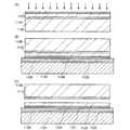
図20(A)に示す単結晶半導体基板1108は清浄化されており、その表面から電界で加速されたイオンを所定の深さに添加し、脆弱化層1110を形成する。イオンの添加は作製基板に転置する単結晶半導体層の厚さを考慮して行われる。イオンを添加する際の加速電圧はこのような厚さを考慮して、単結晶半導体基板1108に添加されるようにする。本発明では、単結晶半導体基板へイオンを添加し、イオンにより微小な空洞を有するように脆弱化された領域を脆弱化層という。A single
単結晶半導体基板1108には、市販の単結晶半導体基板を用いることができ、例えば、単結晶シリコン基板、単結晶ゲルマニウム基板、単結晶シリコンゲルマニウム基板など、第4族元素でなる単結晶半導体基板を用いることができる。また、ガリウムヒ素やインジウムリン等の化合物半導体基板も用いることができる。半導体基板として多結晶半導体基板を用いてもよい。もちろん、単結晶半導体基板は、円形のウエハに限定されるものではなく、様々な形状の単結晶半導体基板を用いることができる。例えば、円形、長方形、五角形、六角形などの多角形の基板を用いることができる。もちろん、市販の円形状の単結晶半導体ウエハを単結晶半導体基板に用いることも可能である。円形状の単結晶半導体ウエハには、シリコンやゲルマニウムなどの半導体ウエハ、ガリウムヒ素やインジウムリンなどの化合物半導体ウエハなどがある。単結晶半導体ウエハの代表例は、単結晶シリコンウエハであり、直径5インチ(125mm)、直径6インチ(150mm)、直径8インチ(200mm)、直径12インチ(300mm)サイズ、直径400mm、直径450mmの円形のウエハを用いることができる。また、長方形の単結晶半導体基板は、市販の円形状の単結晶半導体ウエハを切断することで形成することができる。基板の切断には、ダイサー或いはワイヤソー等の切断装置、レーザ切断、プラズマ切断、電子ビーム切断、その他任意の切断手段を用いることができる。また、基板として薄片化する前の半導体基板製造用のインゴットを、その断面が長方形になるように直方体状に加工し、この直方体状のインゴットを薄片化することでも、長方形状の単結晶半導体基板を製造することができる。また、単結晶半導体基板の厚さは特に限定されないが、単結晶半導体基板を再利用することを考慮すれば、厚い方が1枚の原料ウエハからより多くの単結晶半導体層を形成することができるため、好ましい。市場に流通している単結晶シリコンウエハの厚さは、そのサイズはSEMI規格に準じており、例えば直径6インチのウエハは膜厚625μm、直径8インチのウエハは膜厚725μm、直径12インチのウエハは775μmとされている。なお、SEMI規格のウエハの厚さは公差±25μmを含んでいる。もちろん、原料となる単結晶半導体基板の厚さはSEMI規格に限定されず、インゴットをスライスするときに、その厚さを適宜調節することができる。もちろん、再利用された単結晶半導体基板1108を用いるときには、その厚さは、SEMI規格よりも薄くなる。作製基板上に得られる単結晶半導体層は母体となる半導体基板を選択することによって決定することができる。As the single
また、単結晶半導体基板1108は、作製する半導体素子(本実施の形態においては電界効果トランジスタ)によって、結晶面方位を選択すればよい。例えば、結晶面方位として{100}面、{110}面など有する単結晶半導体基板を用いることができる。Further, the crystal plane orientation of the single
本実施の形態は、単結晶半導体基板の所定の深さに水素、ヘリウム、又はフッ素をイオン添加し、その後熱処理を行って表層の単結晶半導体層を剥離するイオン添加剥離法で形成するが、ポーラスシリコン上に単結晶シリコンをエピタキシャル成長させた後、ポーラスシリコン層をウオータージェットで劈開して剥離する方法を適用しても良い。In this embodiment mode, hydrogen, helium, or fluorine is ion-added to a predetermined depth of the single crystal semiconductor substrate, and then heat treatment is performed to form the surface single crystal semiconductor layer, which is formed by an ion addition peeling method. A method may be applied in which single crystal silicon is epitaxially grown on porous silicon, and then the porous silicon layer is cleaved with a water jet and peeled off.
単結晶半導体基板1108として単結晶シリコン基板を用い、希フッ酸で表面を処理し、自然酸化膜の除去と表面に付着するゴミ等の汚染物も除去して単結晶半導体基板1108表面を清浄化する。A single crystal silicon substrate is used as the single
脆弱化層1110は、イオンをイオンドーピング法(ID法と略記する)やイオン注入法(II法と略記する)によって添加(導入)すればよい。脆弱化層1110は水素、ヘリウム若しくはフッ素に代表されるハロゲンのイオンを添加することで形成される。ハロゲン元素としてフッ素イオンを添加する場合にはソースガスとしてBF3を用いれば良い。なお、イオン注入とはイオン化したガスを質量分離して半導体に添加する方式をいう。The
例えば、イオン注入法を用いて、イオン化した水素ガスを質量分離し、H+のみ、(又はH2+のみ)を選択的に加速して添加することができる。For example, ionized hydrogen gas can be mass-separated using an ion implantation method, and H+ alone (or H2+ alone) can be selectively accelerated and added.
イオンドープ法は、イオン化したガスを質量分離せずに、プラズマ中で複数種のイオン種を作り、それらを加速して単結晶半導体基板にドープする。例えば、H+、H2+、H3+イオンを含む水素では、ドープされるイオンは、代表的にH3+イオンが50%以上、例えばH3+イオンが80%、他のイオン(H+、H2+イオン)が20%、が一般的である。H3+イオンのイオン種のみとして添加することもここではイオンドープとする。In the ion doping method, a plurality of types of ion species are generated in plasma without mass separation of ionized gas, and they are accelerated to dope a single crystal semiconductor substrate. Forexample, H+, H 2+, the hydrogen containingH3 + ions, ions to be doped is typicallyH3 + ions is 50% or more, for exampleH3 + ions is 80%, other ions (H+ , H2+ ion) is typically 20%. Here, adding only as an ion species of H3+ ions is also referred to as ion doping.
また、一又は複数の同一の原子から成る質量の異なるイオンを添加してもよい。例えば、水素イオンを添加する場合には、H+、H2+、H3+イオンを含ませると共に、H3+イオンの割合を高めておくことが好ましい。水素イオンを添加する場合には、H+、H2+、H3+イオンを含ませると共に、H3+イオンの割合を高めておくと添加効率を高めることができ、添加時間を短縮することができる。このような構成とすることで、剥離を容易に行うことができる。In addition, ions having different masses composed of one or a plurality of the same atoms may be added. For example, when hydrogen ions are added, it is preferable to include H+ , H2+ , and H3+ ions and to increase the ratio of H3+ ions. When hydrogen ions are added, H+ , H2+ , H3+ ions are included, and if the ratio of H3+ ions is increased, the addition efficiency can be increased and the addition time can be shortened. Can do. With such a configuration, peeling can be easily performed.
以下、イオンドーピング法とイオン注入法について詳細に説明する。イオンドーピング法に用いるイオンドーピング装置(ID装置ともいう)では、プラズマ空間が大きく、大量のイオンを単結晶半導体基板に添加することができる。一方、イオン注入法に用いるイオン注入装置(II装置ともいう)は、プラズマから取り出したイオンを質量分析して特定のイオン種だけを半導体基板に打ち込めるという特徴があり、基本的に点ビ−ムをスキャンさせて処理する。Hereinafter, the ion doping method and the ion implantation method will be described in detail. In an ion doping apparatus (also referred to as an ID apparatus) used for an ion doping method, a plasma space is large and a large amount of ions can be added to a single crystal semiconductor substrate. On the other hand, an ion implantation apparatus (also referred to as an II apparatus) used for the ion implantation method is characterized by mass-analyzing ions extracted from plasma and implanting only specific ion species into a semiconductor substrate. Scan and process.
プラズマ発生方法としては、どちらの装置も、例えば、フィラメントを熱して出てくる熱電子によりプラズマ状態を作っている。しかし、生成される水素イオン(H+、H2+、H3+)が半導体基板に添加される(打ち込まれる)際の水素イオン種の割合は、イオンドーピング法とイオン注入法で大きく異なる。As a plasma generation method, both apparatuses create a plasma state by, for example, thermoelectrons that are generated by heating a filament. However, the ratio of the hydrogen ion species when the generated hydrogen ions (H+ , H2+ , H3+ ) are added (implanted) to the semiconductor substrate is greatly different between the ion doping method and the ion implantation method.
H3+をより多く打ち込むという観点からすれば、イオン注入装置よりイオンドーピング装置を用いる方が好ましいといえる。From the viewpoint of implanting more H3+ , it can be said that it is preferable to use an ion doping apparatus rather than an ion implantation apparatus.
単結晶シリコン基板に水素イオンやフッ素イオンのようなハロゲンイオンを添加した場合、添加されたフッ素が、シリコン結晶格子内のシリコン原子をノックアウトする(追い出す)ことによって空白部分を効果的に作り出し、脆弱化層に微小な空洞を作る。この場合、比較的低温の熱処理によって脆弱化層に形成された微小な空洞の体積変化が起こり、脆弱化層に沿って劈開することにより薄い単結晶半導体層を形成することができる。フッ素イオンを添加した後に、水素イオンを添加して空洞内に水素を含ませるようにしても良い。単結晶半導体基板から薄い単結晶半導体層を剥離するために形成する脆弱化層は、脆弱化層に形成された微小な空洞の体積変化を利用して劈開をするので、このようにフッ素イオンや水素イオンの作用を有効利用することが好ましい。When halogen ions such as hydrogen ions and fluorine ions are added to a single crystal silicon substrate, the added fluorine effectively creates a blank portion by knocking out (displacing) silicon atoms in the silicon crystal lattice, and is fragile. Create a small cavity in the layer. In this case, a volume change of a minute cavity formed in the weakened layer occurs by heat treatment at a relatively low temperature, and a thin single crystal semiconductor layer can be formed by cleaving along the weakened layer. After adding fluorine ions, hydrogen ions may be added so that the cavities contain hydrogen. The weakening layer formed to peel the thin single crystal semiconductor layer from the single crystal semiconductor substrate is cleaved by utilizing the volume change of a minute cavity formed in the weakening layer. It is preferable to effectively use the action of hydrogen ions.
また、単結晶半導体基板と上記単結晶半導体層と接合する無機絶縁膜(又は絶縁層)との間に、保護層を形成してもよい。保護層は、窒化シリコン層、酸化シリコン層、窒化酸化シリコン層、又は酸化窒化シリコン層から選ばれた一層又は複数の層による積層構造により形成することができる。これらの層は、単結晶半導体基板に脆弱化層が形成される前に単結晶半導体基板上に形成することができる。また、単結晶半導体基板に脆弱化層を形成した後に単結晶半導体基板上に形成してもよい。Further, a protective layer may be formed between the single crystal semiconductor substrate and the inorganic insulating film (or insulating layer) bonded to the single crystal semiconductor layer. The protective layer can be formed by a single layer or a stacked layer structure including a plurality of layers selected from a silicon nitride layer, a silicon oxide layer, a silicon nitride oxide layer, and a silicon oxynitride layer. These layers can be formed over the single crystal semiconductor substrate before the weakening layer is formed over the single crystal semiconductor substrate. Alternatively, the weakening layer may be formed over the single crystal semiconductor substrate and then formed over the single crystal semiconductor substrate.
脆弱化層の形成に当たってはイオンを高ドーズ条件で添加する必要があり、単結晶半導体基板1108の表面が粗くなってしまう場合がある。そのためイオンが添加される表面に窒化シリコン膜、窒化酸化シリコン膜、若しくは酸化シリコン膜などによりイオン添加に対する保護層を50nm乃至200nmの厚さで設けておいても良い。In forming the weakened layer, ions must be added under a high dose condition, and the surface of the single
例えば、単結晶半導体基板1108上に保護層としてプラズマCVD法により酸化窒化シリコン膜(膜厚5nm〜300nm、望ましくは30nm〜150nm(例えば50nm))と窒化酸化シリコン膜(膜厚5nm〜150nm、望ましくは10nm〜100nm(例えば50nm))の積層を形成する。一例としては、単結晶半導体基板1108上に酸化窒化シリコン膜を膜厚50nm形成し、該酸化窒化シリコン膜上に窒化酸化シリコン膜を膜厚50nm形成し、積層する。酸化窒化シリコン膜は有機シランガスを用いて化学気相成長法により作製される酸化シリコン膜でもよい。For example, a silicon oxynitride film (film thickness: 5 nm to 300 nm, desirably 30 nm to 150 nm (eg, 50 nm)) and a silicon nitride oxide film (film thickness: 5 nm to 150 nm, desirably, as a protective layer over the single
また、単結晶半導体基板1108を脱脂洗浄し、表面の酸化膜を除去して熱酸化を行ってもよい。熱酸化としては通常のドライ酸化でも良いが、酸化雰囲気中にハロゲンを添加した酸化を行うことが好ましい。例えば、酸素に対しHClを0.5〜10体積%(好ましくは3体積%)の割合で含む雰囲気中で、700℃以上の温度で熱処理を行う。好適には950℃〜1100℃の温度で熱酸化を行うと良い。処理時間は0.1〜6時間、好ましくは0.5〜3.5時間とすれば良い。形成される酸化膜の膜厚としては、10nm〜1000nm(好ましくは50nm〜200nm)、例えば100nmの厚さとする。Alternatively, the single
ハロゲンを含むものとしてはHClの他に、HF、NF3、HBr、Cl2、ClF3、BCl3、F2、Br2などから選ばれた一種又は複数種を適用することができる。In addition to HCl, one or more selected from HF, NF3 , HBr, Cl2 , ClF3 , BCl3 , F2 , Br2 and the like can be used as the halogen-containing material.
このような温度範囲で熱処理を行うことで、ハロゲン元素によるゲッタリング効果を得ることができる。ゲッタリングとしては、特に金属不純物を除去する効果がある。すなわち、塩素の作用により、金属などの不純物が揮発性の塩化物となって気相中へ離脱して除去される。単結晶半導体基板1108の表面を化学的機械研磨(CMP)処理をしたものに対しては有効である。また、水素は単結晶半導体基板1108と形成される無機絶縁膜(又は絶縁層)の界面の欠陥を補償して界面の局在準位密度を低減する作用を奏し、単結晶半導体基板1108と無機絶縁膜(又は絶縁層)との界面が不活性化されて電気的特性が安定化する。By performing heat treatment in such a temperature range, a gettering effect by a halogen element can be obtained. Gettering is particularly effective in removing metal impurities. That is, by the action of chlorine, impurities such as metals become volatile chlorides and are released into the gas phase and removed. This is effective for the surface of the single
この熱処理により形成される酸化膜中にハロゲンを含ませることができる。ハロゲン元素は1×10¹⁷/cm3〜5×1020/cm3の濃度で含まれることにより金属などの不純物を捕獲して単結晶半導体基板1108の汚染を防止する保護層としての機能を発現させることができる。Halogen can be contained in the oxide film formed by this heat treatment. The halogen element is contained at a concentration of 1 × 10¹⁷ / cm3 to 5 × 10²⁰ / cm3 so that it functions as a protective layer that captures impurities such as metal and prevents contamination of the single
脆弱化層1110を形成する際、加速電圧と全イオン数は、単結晶半導体基板上に堆積した膜の厚さと、目的とする単結晶半導体基板より分離して作製基板上に転置される単結晶半導体層の膜厚と、添加するイオン種によって調整することができる。When the
例えば、イオンドーピング法で原料として水素ガスを用い、加速電圧を40kV、全イオン数2×10¹⁶ions/cm2でイオンを添加して脆弱化層を形成することができる。保護層の膜厚を厚くすれば、同一条件でイオンを添加し脆弱化層を形成した場合、目的とする単結晶半導体基板より分離して作製基板上に転置(転載)される単結晶半導体層として、膜厚の薄い単結晶半導体層を形成することができる。例えば、イオン種(H+、H2+、H3+イオン)の割合にもよるが、上記条件で脆弱化層を形成するとし、保護層として単結晶半導体基板上に酸化窒化シリコン膜(膜厚50nm)と窒化酸化シリコン膜(膜厚50nm)を保護層として積層する場合、作製基板に転置される単結晶半導体層の膜厚は約120nmとなり、単結晶半導体基板上に酸化窒化シリコン膜(膜厚100nm)と窒化酸化シリコン膜(膜厚50nm)を保護層として積層する場合は、作製基板に転置される単結晶半導体層の膜厚は約70nmとなる。For example, the weakened layer can be formed by using hydrogen gas as a raw material in the ion doping method, adding ions at an acceleration voltage of 40 kV, and a total number of ions of 2 × 10¹⁶ ions / cm2 . If the thickness of the protective layer is increased, when a weakened layer is formed by adding ions under the same conditions, the single crystal semiconductor layer is separated from the target single crystal semiconductor substrate and transferred (transferred) onto the formation substrate. As described above, a thin single crystal semiconductor layer can be formed. For example, although depending on the ratio of ion species (H+ , H2+ , H3+ ions), a weakened layer is formed under the above conditions, and a silicon oxynitride film (film) is formed on the single crystal semiconductor substrate as a protective layer. When a protective layer is formed by stacking a silicon nitride oxide film (thickness 50 nm) and a silicon nitride oxide film (film thickness 50 nm), the thickness of the single crystal semiconductor layer transferred to the formation substrate is approximately 120 nm, and a silicon oxynitride film ( In the case of stacking a protective film with a thickness of 100 nm and a silicon nitride oxide film (with a thickness of 50 nm), the thickness of the single crystal semiconductor layer transferred to the manufacturing substrate is approximately 70 nm.
ヘリウム(He)や水素を原料ガスにする場合、加速電圧を10kV〜200kVの範囲で、ドーズ量を1×10¹⁶ions/cm2〜6×1016ions/cm2の範囲で添加し脆弱化層を形成することができる。ヘリウムを原料ガスにすると、質量分離を行わなくてもHe+イオンを主なイオンとして添加することができる。また、水素を原料ガスとするとH3+イオンやH2+イオンを主なイオンとして添加することができる。イオン種は、プラズマの生成方法、圧力、原料ガス供給量、加速電圧によっても変化する。When helium (He) or hydrogen is used as a source gas, it is weakened by adding an acceleration voltage in the range of 10 kV to 200 kV and a dose amount in the range of 1 × 10¹⁶ ions / cm2 to 6 × 10¹⁶ ions / cm2 . A layer can be formed. When helium is used as a source gas, He+ ions can be added as main ions without mass separation. In addition, when hydrogen is used as a source gas, H3+ ions and H2+ ions can be added as main ions. The ion species also varies depending on the plasma generation method, pressure, source gas supply amount, and acceleration voltage.
脆弱化層形成の例としては、単結晶半導体基板上に酸化窒化シリコン膜(膜厚50nm)、窒化酸化シリコン膜(膜厚50nm)、及び酸化シリコン膜(膜厚50nm)を保護層として積層し、水素を加速電圧40kV、ドーズ量2×10¹⁶ions/cm2で添加し単結晶半導体基板に脆弱化層を形成する。その後保護層の最上層である該酸化シリコン膜上に接合面を有する絶縁層として酸化シリコン膜(膜厚50nm)を形成する。脆弱化層形成の他の例としては、単結晶半導体基板上に酸化シリコン膜(膜厚100nm)、及び窒化酸化シリコン膜(膜厚50nm)を保護層として積層し、水素を加速電圧40kV、ドーズ量2×1016ions/cm2で添加し単結晶半導体基板に脆弱化層を形成する。その後保護層の最上層である該窒化酸化シリコン膜上に接合面を有する絶縁層として酸化シリコン膜(膜厚50nm)を形成する。なお、上記酸化窒化シリコン膜及び窒化酸化シリコン膜はプラズマCVD法により形成すればよく、上記酸化シリコン膜は有機シランガスを用いてCVD法により形成すればよい。As an example of forming a weakened layer, a silicon oxynitride film (film thickness 50 nm), a silicon nitride oxide film (film thickness 50 nm), and a silicon oxide film (film thickness 50 nm) are stacked as a protective layer over a single crystal semiconductor substrate. Hydrogen is added at an acceleration voltage of 40 kV and a dose of 2 × 10¹⁶ ions / cm2 to form a weakened layer on the single crystal semiconductor substrate. Thereafter, a silicon oxide film (film thickness: 50 nm) is formed as an insulating layer having a bonding surface over the silicon oxide film which is the uppermost layer of the protective layer. As another example of forming the weakened layer, a silicon oxide film (film thickness: 100 nm) and a silicon nitride oxide film (film thickness: 50 nm) are stacked over a single crystal semiconductor substrate as a protective layer, and hydrogen is accelerated at a voltage of 40 kV and a dose. An amount of 2 × 10¹⁶ ions / cm2 is added to form a weakened layer on the single crystal semiconductor substrate. After that, a silicon oxide film (film thickness: 50 nm) is formed as an insulating layer having a bonding surface over the silicon nitride oxide film which is the uppermost layer of the protective layer. Note that the silicon oxynitride film and the silicon nitride oxide film may be formed by a plasma CVD method, and the silicon oxide film may be formed by a CVD method using an organosilane gas.
また、無機絶縁膜と単結晶半導体基板との間に絶縁層を形成してもよい。絶縁層は無機絶縁膜側、あるいは単結晶半導体基板側どちらか一方でもよいし、両方に形成してもよい。接合を形成する面に形成する絶縁層は平滑面を有し親水性表面を形成する。該絶縁層としては、酸化シリコン膜を用いることができる。酸化シリコン膜としては有機シランガスを用いて化学気相成長法により作製される酸化シリコン膜が好ましい。その他に、シランガスを用いて化学気相成長法により作製される酸化シリコン膜を適用することもできる。An insulating layer may be formed between the inorganic insulating film and the single crystal semiconductor substrate. The insulating layer may be formed on either the inorganic insulating film side, the single crystal semiconductor substrate side, or both. The insulating layer formed on the surface where the bond is formed has a smooth surface and forms a hydrophilic surface. As the insulating layer, a silicon oxide film can be used. As the silicon oxide film, a silicon oxide film formed by a chemical vapor deposition method using an organosilane gas is preferable. In addition, a silicon oxide film manufactured by a chemical vapor deposition method using silane gas can be used.
有機シランガスとしては、珪酸エチル(TEOS:化学式Si(OC2H5)4)、トリメチルシラン(TMS:(CH3)3SiH)、テトラメチルシラン(化学式Si(CH3)4)、テトラメチルシクロテトラシロキサン(TMCTS)、オクタメチルシクロテトラシロキサン(OMCTS)、ヘキサメチルジシラザン(HMDS)、トリエトキシシラン(SiH(OC2H5)3)、トリスジメチルアミノシラン(SiH(N(CH3)2)3)等のシリコン含有化合物を用いることができる。なお、原料ガスに有機シランを用いて化学気相成長法により酸化シリコン層を形成する場合、酸素を付与するガスを混合させることが好ましい。酸素を付与するガスとしては、酸素、亜酸化窒素、二酸化窒素等を用いることができる。さらに、アルゴン、ヘリウム、窒素又は水素等の不活性ガスを混合させてもよい。Examples of the organic silane gas include ethyl silicate (TEOS: chemical formula Si (OC2 H5 )4 ), trimethylsilane (TMS: (CH3 )3 SiH), tetramethylsilane (chemical formula Si (CH3 )4 ), tetramethylcyclo Tetrasiloxane (TMCTS), octamethylcyclotetrasiloxane (OMCTS), hexamethyldisilazane (HMDS), triethoxysilane (SiH (OC2 H5 )3 ), trisdimethylaminosilane (SiH (N (CH3 )2 )3 ) and other silicon-containing compounds can be used. Note that in the case where a silicon oxide layer is formed by a chemical vapor deposition method using organosilane as a source gas, it is preferable to mix an oxygen-providing gas. As a gas for imparting oxygen, oxygen, nitrous oxide, nitrogen dioxide, or the like can be used. Further, an inert gas such as argon, helium, nitrogen or hydrogen may be mixed.
また、接合を形成する面に形成する絶縁層として、モノシラン、ジシラン、又はトリシラン等のシランを原料ガスに用いて化学気相成長法により形成される酸化シリコン膜を適用することもできる。この場合も、酸素を付与するガスや不活性ガス等を混合させることが好ましい。また、単結晶半導体層と接合する絶縁層となる酸化シリコン膜は、塩素を含んでいてもよい。なお、本明細書において、化学気相成長(CVD;Chemical Vapor Deposition)法は、プラズマCVD法、熱CVD法、光CVD法を範疇に含む。Alternatively, a silicon oxide film formed by a chemical vapor deposition method using silane such as monosilane, disilane, or trisilane as a source gas can be used as an insulating layer formed on a surface where a bond is formed. Also in this case, it is preferable to mix an oxygen-providing gas, an inert gas, or the like. Further, the silicon oxide film to be an insulating layer bonded to the single crystal semiconductor layer may contain chlorine. Note that in this specification, a chemical vapor deposition (CVD) method includes, in its category, a plasma CVD method, a thermal CVD method, and a photo CVD method.
その他、接合を形成する面に形成する絶縁層として、酸化性雰囲気下において熱処理することにより形成される酸化シリコン、酸素ラジカルの反応により成長する酸化シリコン、酸化性の薬液により形成されるケミカルオキサイドなどを適用することもできる。絶縁層として、シロキサン(Si−O−Si)結合を含む絶縁層を適用してもよい。また、前記有機シランガスと、酸素ラジカル又は窒素ラジカルとを反応させて絶縁層を形成してもよい。In addition, as an insulating layer formed on the surface to form a bond, silicon oxide formed by heat treatment in an oxidizing atmosphere, silicon oxide grown by reaction of oxygen radicals, chemical oxide formed by an oxidizing chemical, etc. Can also be applied. An insulating layer containing a siloxane (Si—O—Si) bond may be used as the insulating layer. Further, the insulating layer may be formed by reacting the organic silane gas with oxygen radicals or nitrogen radicals.
無機絶縁膜、絶縁層において、接合を形成する面の表面は、算術平均粗さRaが0.8nm未満、二乗平均平方根粗さRmsが0.9nm未満が望ましく、Raが0.4nm以下、Rmsが0.5nm以下がより望ましく、さらにはRaが0.3nm以下、Rmsが0.4nm以下がより望ましい。例えば、Raが0.27nm、Rmsが0.34nmである。本明細書においてRaは算術平均粗さであり、Rmsは二乗平均平方根粗さであり、測定範囲は2μm2、又は10μm2である。In the inorganic insulating film and the insulating layer, the surface of the surface where the junction is formed preferably has an arithmetic average roughness Ra of less than 0.8 nm, a root mean square roughness Rms of less than 0.9 nm, Ra of 0.4 nm or less, and Rms. Is more preferably 0.5 nm or less, more preferably Ra is 0.3 nm or less and Rms is 0.4 nm or less. For example, Ra is 0.27 nm and Rms is 0.34 nm. In this specification, Ra is the arithmetic mean roughness, Rms is the root mean square roughness, and the measurement range is 2 μm2 or 10 μm2 .
無機絶縁膜と単結晶半導体基板とを接合するに際し、接合を形成する面の一方若しくは双方に、好ましくは有機シランを原材料として成膜した酸化シリコン膜でなる絶縁層を設けると強固な接合を形成することができる。When an inorganic insulating film and a single crystal semiconductor substrate are bonded, an insulating layer made of a silicon oxide film, preferably formed using organosilane as a raw material, is provided on one or both surfaces of the bonding to form a strong bond. can do.
本実施の形態では、図20(B)で示すように無機絶縁膜と接合を形成する面に絶縁層1104として酸化シリコン膜を形成する。酸化シリコン膜としては有機シランガスを用いて化学気相成長法により作製される酸化シリコン膜が好ましい。その他に、シランガスを用いて化学気相成長法により作製される酸化シリコン膜を適用することもできる。化学気相成長法による成膜では、単結晶半導体基板に形成した脆弱化層1110から脱ガスが起こらない温度として、例えば350℃以下(具体的な例としては300℃)の成膜温度が適用される。また、単結晶半導体基板から単結晶半導体層を剥離する熱処理は、成膜温度よりも高い熱処理温度が適用される。In this embodiment, as illustrated in FIG. 20B, a silicon oxide film is formed as the insulating
本実施の形態では、作製基板上で半導体素子層を形成後、半導体素子層を作製基板より剥離するため、作製基板と半導体素子層との間に剥離層を設ける。よって単結晶半導体基板より分離して接合される単結晶半導体層は、作製基板上に設けられた剥離層及び無機絶縁膜上に形成される。剥離層表面に凹凸を有すると、単結晶半導体基板と作製基板との接合工程において、接合面の接触面積が小さくなり、十分な接合強度を確保することが困難である。そのため、剥離層を平坦化する工程が必要である。In this embodiment, after the semiconductor element layer is formed over the manufacturing substrate, the separation layer is provided between the manufacturing substrate and the semiconductor element layer in order to peel the semiconductor element layer from the manufacturing substrate. Therefore, the single crystal semiconductor layer which is separated and bonded from the single crystal semiconductor substrate is formed over the separation layer and the inorganic insulating film provided over the manufacturing substrate. When the surface of the separation layer is uneven, the contact area of the bonding surface is reduced in the bonding process between the single crystal semiconductor substrate and the manufacturing substrate, and it is difficult to ensure sufficient bonding strength. Therefore, a process for flattening the release layer is necessary.
図18(A)において作製基板1101上に剥離層1130が形成されている。剥離層1130に平坦化処理を行うことによって表面が平坦化された剥離層1125を形成する(図18(B)参照。)。平坦化された剥離層1125上に無機絶縁膜1109を形成すると、無機絶縁膜1109表面も平坦性を高くすることができる(図18(C)参照。)。In FIG. 18A, a
平坦化処理としては、研磨処理やエッチング処理を行えばよく、勿論、研磨処理及びエッチング処理を両方行ってもよい。研磨処理としては、化学的機械研磨(CMP)法や液体ジェット研磨法を用いることができる。エッチング処理としては、ウェットエッチング、ドライエッチング、またはその両方を適宜用いることができる。As the planarization process, a polishing process or an etching process may be performed. Of course, both the polishing process and the etching process may be performed. As the polishing treatment, a chemical mechanical polishing (CMP) method or a liquid jet polishing method can be used. As the etching treatment, wet etching, dry etching, or both can be used as appropriate.
またプラズマ処理によって平坦化処理を行ってもよい。例えば、逆スパッタリング法を用いることができる。逆スパッタリング法にて平坦化処理を行うと、無機絶縁膜や無機絶縁層の形成から平坦化までを同一装置内にて行うことができるため、スループットが向上し、好ましい。Further, planarization treatment may be performed by plasma treatment. For example, a reverse sputtering method can be used. When planarization is performed by a reverse sputtering method, formation from an inorganic insulating film or an inorganic insulating layer to planarization can be performed in the same apparatus, which is preferable because throughput is improved.
逆スパッタリング法は、例えば、高真空のチャンバーに不活性ガス、例えばArガスを導入し、被処理面に対して電界をかけることでプラズマ状態として行う。プラズマ中には電子とArの陽イオンが存在し、陰極方向にArの陽イオンが加速される。加速されたArの陽イオンは被処理面をスパッタする。このとき、該被処理面の凸部から優先的にスパッタされる。被処理面からスパッタされた粒子は、被処理面の別の場所に付着する。このとき、該被処理面の凹部に優先的に付着する。このように凸部を削り、凹部を埋めることで被処理面の平坦性が向上すると考えられる。In the reverse sputtering method, for example, an inert gas such as Ar gas is introduced into a high-vacuum chamber, and an electric field is applied to the surface to be processed so that the plasma state is obtained. There are electrons and Ar cations in the plasma, and the Ar cations are accelerated in the cathode direction. The accelerated Ar cations sputter the surface to be processed. At this time, sputtering is preferentially performed from the convex portion of the surface to be processed. The particles sputtered from the surface to be processed adhere to another place on the surface to be processed. At this time, it preferentially adheres to the concave portion of the surface to be processed. Thus, it is thought that the flatness of the surface to be processed is improved by cutting the convex portion and filling the concave portion.
本実施の形態では、剥離層をスパッタリング法で形成し、逆スパッタリング法によって平坦化処理を行う。In this embodiment mode, the separation layer is formed by a sputtering method and planarized by a reverse sputtering method.
作製基板には、剥離層との間に不純物元素の拡散を防止する窒化シリコン膜又は窒化酸化シリコン膜をブロッキング層(バリア層ともいう)として設けてもよい。さらに応力を緩和する作用のある絶縁膜として酸化窒化シリコン膜を組み合わせても良い。A silicon nitride film or a silicon nitride oxide film that prevents diffusion of an impurity element may be provided as a blocking layer (also referred to as a barrier layer) between the separation substrate and the separation layer. Further, a silicon oxynitride film may be combined as an insulating film having a function of relieving stress.
図20(C)は作製基板1101上に設けられた無機絶縁膜1109と単結晶半導体基板1108の絶縁層1104が形成された面とを密接させ、この両者を接合させる態様を示す。無機絶縁膜1109表面は平坦化された剥離層1125上に設けられているために表面は高い平坦性を有している。接合を形成する面は、十分に清浄化しておく。作製基板1101上に設けられた無機絶縁膜1109と単結晶半導体基板1108の絶縁層1104が形成された面は、メガソニック洗浄などによって清浄化すればよい。また、メガソニック洗浄後にオゾン水で洗浄し、有機物の除去と表面の親水性向上を行ってもよい。FIG. 20C illustrates a mode in which the inorganic insulating
作製基板1101上の無機絶縁膜1109と絶縁層1104とを対向させて、一箇所を外部から押しつけると、局所的に接合面同士の距離が縮まる事によるファン・デル・ワールス力の強まりや水素結合の寄与によって、お互いに引きつけ合う。更に、隣接した領域でも対向する作製基板1101上の無機絶縁膜1109と絶縁層1104との間の距離が縮まるので、ファン・デル・ワールス力が強く作用する領域や水素結合が関与する領域が広がる事によって、接合(ボンディングともいう)が進行し接合面全域に接合が広がる。例えば、押しつける圧力は、100kPa〜5000kPa程度とすればよい。また、支持基板と半導体基板とを重ねるように配置し、重ねる基板の重みでも接合を広げることもできる。When the inorganic insulating
良好な接合を形成するために、表面を活性化しておいても良い。例えば、接合を形成する面に原子ビーム若しくはイオンビームを照射する。原子ビーム若しくはイオンビームを利用する場合には、アルゴン等の不活性ガス中性原子ビーム若しくは不活性ガスイオンビームを用いることができる。その他に、プラズマ照射若しくはラジカル処理を行う。このような表面処理により200℃乃至400℃の温度であっても異種材料間の接合を形成することが容易となる。In order to form a good bond, the surface may be activated. For example, an atomic beam or an ion beam is irradiated to the surface on which the junction is formed. When an atomic beam or an ion beam is used, an inert gas neutral atom beam or inert gas ion beam such as argon can be used. In addition, plasma irradiation or radical treatment is performed. Such surface treatment makes it easy to form a bond between different materials even at a temperature of 200 ° C. to 400 ° C.
また、作製基板と絶縁層との接合界面の接合強度を向上させるために、加熱処理を行うと好ましい。例えば、オーブンや炉などで70℃〜350℃(例えば200℃で2時間)の温度条件で熱処理を行う。In addition, heat treatment is preferably performed in order to improve the bonding strength at the bonding interface between the manufacturing substrate and the insulating layer. For example, heat treatment is performed in a temperature condition of 70 ° C. to 350 ° C. (for example, 200 ° C. for 2 hours) in an oven or a furnace.
図20(D)において、作製基板1101と単結晶半導体基板1108を貼り合わせた後、加熱処理を行い脆弱化層1110を劈開面として単結晶半導体基板1108を作製基板1101から剥離する。例えば、400℃〜700℃の熱処理を行うことにより、脆弱化層1110に形成された微小な空洞の体積変化が起こり、脆弱化層1110に沿って劈開することが可能となる。絶縁層1104は無機絶縁膜1109を介して作製基板1101と接合しているので、作製基板1101上には単結晶半導体基板1108と同じ結晶性の単結晶半導体層1102が残存することとなる。20D, after the
400℃〜700℃の温度域での熱処理は、前述の接合強度を向上させるための熱処理と同じ装置で連続して行ってもよいし、別の装置で行ってもよい。例えば炉で200℃2時間熱処理した後に、600℃近傍まで昇温し2時間保持し、400℃から室温までの温度域に降温した後炉より取り出す。また、熱処理は室温から昇温してもよい。また、炉で200℃2時間熱処理した後に、瞬間熱アニール(RTA)装置によって600℃〜700℃の温度域で、1分間〜30分間(例えば600℃7分間、650℃7分間)熱処理を行ってもよい。The heat treatment in the temperature range of 400 ° C. to 700 ° C. may be continuously performed with the same apparatus as the heat treatment for improving the above-described bonding strength, or may be performed with another apparatus. For example, after heat treatment at 200 ° C. for 2 hours in a furnace, the temperature is raised to near 600 ° C., held for 2 hours, the temperature is lowered to a temperature range from 400 ° C. to room temperature, and then removed from the furnace. Further, the heat treatment may be performed from room temperature. In addition, after heat treatment at 200 ° C. for 2 hours in a furnace, heat treatment is performed in a temperature range of 600 ° C. to 700 ° C. for 1 minute to 30 minutes (for example, 600 ° C. for 7 minutes, 650 ° C. for 7 minutes) using a rapid thermal annealing (RTA) apparatus. May be.
400℃〜700℃の温度域での熱処理により、絶縁層と作製基板との接合は水素結合から共有結合に移行し、脆弱化層に添加された元素が析出し圧力が上昇し、単結晶半導体基板より単結晶半導体層を剥離することができる。熱処理を行った後は作製基板と単結晶半導体基板は、一方が他方に載っている状態であり、大きな力を加えずに作製基板と単結晶半導体基板を離すことができる。例えば、上方に載っている基板を真空チャックで持ち上げることにより簡単に離すことができる。この際、下側の基板の真空チャックやメカニカルチャックで固定しておくと水平方向のずれがなく作製基板及び単結晶半導体基板の両基板を離すことができる。By heat treatment in a temperature range of 400 ° C. to 700 ° C., the bonding between the insulating layer and the manufacturing substrate is changed from a hydrogen bond to a covalent bond, and an element added to the weakened layer is precipitated and the pressure is increased. The single crystal semiconductor layer can be peeled from the substrate. After the heat treatment, one of the manufacturing substrate and the single crystal semiconductor substrate is placed on the other, and the manufacturing substrate and the single crystal semiconductor substrate can be separated without applying a large force. For example, the substrate placed above can be easily separated by lifting it with a vacuum chuck. At this time, if the lower substrate is fixed with a vacuum chuck or a mechanical chuck, both the production substrate and the single crystal semiconductor substrate can be separated without horizontal displacement.
なお、図20、図21においては、単結晶半導体基板1108が作製基板1101より小さいサイズの例を示すが、本発明はそれに限定されず、単結晶半導体基板1108と作製基板1101が同じサイズであってもよいし、単結晶半導体基板1108が作製基板1101より大きいサイズであってもよい。20 and 21 illustrate examples in which the single
図21は作製基板側に絶縁層を設けて単結晶半導体層を形成する工程を示す。図21(A)は保護層1121として酸化シリコン膜が形成された単結晶半導体基板1108に電界で加速されたイオンを所定の深さに添加し、脆弱化層1110を形成する工程を示している。イオンの添加は図20(A)の場合と同様である。単結晶半導体基板1108の表面に保護層1121を形成しておくことでイオン添加によって表面がダメージを受け、平坦性が損なわれるのを防ぐことができる。また、保護層1121によって、単結晶半導体基板1108から形成される単結晶半導体層1102に対する不純物の拡散防止効果を発現する。FIG. 21 shows a step of forming a single crystal semiconductor layer by providing an insulating layer on the manufacturing substrate side. FIG. 21A shows a step of forming a weakened
図21(B)は、無機絶縁膜1109及び絶縁層1104が形成された作製基板1101と単結晶半導体基板1108の保護層1121が形成された面を密着させて接合を形成する工程を示している。作製基板1101上の絶縁層1104と単結晶半導体基板1108の保護層1121を密着させることにより接合が形成される。FIG. 21B illustrates a process in which the
その後、図21(C)で示すように単結晶半導体基板1108を剥離する。単結晶半導体層を剥離する熱処理は図20(D)の場合と同様にして行う。このようにして図21(C)で示す絶縁層を介して単結晶半導体層を有する本発明のSOI構造の半導体基板を得ることができる。After that, the single
また、単結晶半導体基板より分離し、作製基板に転置された単結晶半導体層は、分離工程およびイオン照射工程によって、結晶欠陥が生じ、また、その表面は平坦性が損なわれ、凹凸が形成されてしまう場合がある。単結晶半導体層を用いて半導体素子としてトランジスタを作製する場合、このような凹凸のある単結晶半導体層の上面に薄く、絶縁耐圧性の高いゲート絶縁層を形成することは困難である。また、単結晶半導体層に結晶欠陥があると、ゲート絶縁層との局在界面準位密度が高くなるなど、トランジスタの性能および信頼性に影響を与える。In addition, the single crystal semiconductor layer separated from the single crystal semiconductor substrate and transferred to the formation substrate has crystal defects caused by the separation step and the ion irradiation step, and the surface is not flat and uneven. May end up. In the case of manufacturing a transistor as a semiconductor element using a single crystal semiconductor layer, it is difficult to form a thin gate insulating layer with high withstand voltage on the top surface of the uneven single crystal semiconductor layer. In addition, a crystal defect in the single crystal semiconductor layer affects the performance and reliability of the transistor, such as an increase in the density of localized interface states with the gate insulating layer.
従って単結晶半導体層にレーザ光のような電磁波を照射し、結晶欠陥を低減させることが好ましい。電磁波を照射することによって、単結晶半導体層の少なくとも一部の領域を溶融させ、単結晶半導体層中の結晶欠陥を低減させることができる。なお、電磁波の照射前に単結晶半導体層表面に形成された酸化膜(自然酸化膜、あるいはケミカル酸化膜)を希フッ酸で除去するとよい。Accordingly, it is preferable to reduce crystal defects by irradiating the single crystal semiconductor layer with electromagnetic waves such as laser light. By irradiation with electromagnetic waves, at least part of the single crystal semiconductor layer can be melted and crystal defects in the single crystal semiconductor layer can be reduced. Note that an oxide film (a natural oxide film or a chemical oxide film) formed on the surface of the single crystal semiconductor layer is preferably removed with dilute hydrofluoric acid before irradiation with electromagnetic waves.
電磁波は単結晶半導体層に高いエネルギーを供給できるものであればよく、好適にはレーザ光を用いることができる。Any electromagnetic wave may be used as long as it can supply high energy to the single crystal semiconductor layer, and laser light can be preferably used.
またエネルギーの供給は、高エネルギーを有する粒子を照射などによって単結晶半導体層に衝突させ、主として熱伝導によって行うこともできる。高エネルギーを有する粒子を提供する熱源としては、プラズマを用いることができ、常圧プラズマ、高圧プラズマ、熱プラズマジェット、ガスバーナーなどの炎を用いることができる、又、他の熱源としては電子ビームなどを用いることができる。The energy can also be supplied mainly by heat conduction by causing particles having high energy to collide with the single crystal semiconductor layer by irradiation or the like. As a heat source for providing particles having high energy, a plasma can be used, and a flame such as an atmospheric plasma, a high pressure plasma, a thermal plasma jet, a gas burner can be used, and an electron beam is used as another heat source. Etc. can be used.
電磁波の波長は、単結晶半導体層に吸収される波長とする。その波長は、電磁波の表皮深さ(skin depth)などを考慮して決定することができる。例えば、電磁波の波長は190nm〜600nmを用いることができる。また、電磁波のエネルギーは、電磁波の波長、電磁波の表皮深さ、照射する単結晶半導体層の膜厚などを考慮して決定することができる。The wavelength of the electromagnetic wave is a wavelength that is absorbed by the single crystal semiconductor layer. The wavelength can be determined in consideration of the skin depth of the electromagnetic wave. For example, the wavelength of the electromagnetic wave can be 190 nm to 600 nm. The energy of the electromagnetic wave can be determined in consideration of the wavelength of the electromagnetic wave, the skin depth of the electromagnetic wave, the thickness of the single crystal semiconductor layer to be irradiated, and the like.
レーザ光を発振するレーザは、連続発振レーザ、疑似連続発振レーザ及びパルス発振レーザを用いることができる。部分溶融させるためパルス発振レーザが好ましい。例えば、KrFレーザなどのエキシマレーザ、Arレーザ、Krレーザなどの気体レーザがある。その他、固体レーザとして、YAGレーザ、YVO4レーザ、YLFレーザ、YAlO3レーザ、GdVO4レーザ、KGWレーザ、KYWレーザ、アレキサンドライトレーザ、Ti:サファイアレーザ、Y2O3レーザなどがある。なお、エキシマレーザはパルス発振レーザであるが、YAGレーザなどの固体レーザには、連続発振レーザにも、疑似連続発振レーザにも、パルス発振レーザにもなるものがある。なお、固体レーザにおいては、基本波の第2高調波〜第5高調波を適用するのが好ましい。また、GaN、GaAs、GaAlAs、InGaAsP等の半導体レーザも用いることができる。As a laser that oscillates laser light, a continuous wave laser, a pseudo continuous wave laser, or a pulsed laser can be used. A pulsed laser is preferable for partial melting. For example, there is an excimer laser such as a KrF laser, or a gas laser such as an Ar laser or a Kr laser. Other solid-state lasers include YAG laser, YVO4 laser, YLF laser, YAlO3 laser, GdVO4 laser, KGW laser, KYW laser, alexandrite laser, Ti: sapphire laser, and Y2 O3 laser. An excimer laser is a pulsed laser, but some solid-state lasers such as a YAG laser can be a continuous wave laser, a pseudo continuous wave laser, or a pulsed laser. In the solid-state laser, it is preferable to apply the second to fifth harmonics of the fundamental wave. A semiconductor laser such as GaN, GaAs, GaAlAs, InGaAsP, or the like can also be used.
また、電磁波のエネルギーを単結晶半導体層に照射できるならば、ランプ光を用いてもよい。例えば、紫外線ランプ、ブラックライト、ハロゲンランプ、メタルハライドランプ、キセノンアークランプ、カーボンアークランプ、高圧ナトリウムランプ、または高圧水銀ランプから射出された光を用いてもよい。上記ランプ光を用いたフラッシュアニールを用いてもよい。ハロゲンランプやキセノンランプなどを好適に用いて行うフラッシュアニールは極短時間の処理でよいため、作製基板の温度上昇を抑えることができる。If the single crystal semiconductor layer can be irradiated with electromagnetic wave energy, lamp light may be used. For example, light emitted from an ultraviolet lamp, black light, halogen lamp, metal halide lamp, xenon arc lamp, carbon arc lamp, high pressure sodium lamp, or high pressure mercury lamp may be used. Flash annealing using the lamp light may be used. Flash annealing that is preferably performed using a halogen lamp, a xenon lamp, or the like can be performed in an extremely short time, and thus the temperature rise of the manufacturing substrate can be suppressed.
電磁波の形状や電磁波の進路を調整するため、シャッター、ミラー又はハーフミラー等の反射体、シリンドリカルレンズや凸レンズなどによって構成される光学系が設置されていてもよい。In order to adjust the shape of the electromagnetic wave and the path of the electromagnetic wave, an optical system including a reflector such as a shutter, a mirror or a half mirror, a cylindrical lens, or a convex lens may be installed.
なお、電磁波の照射方法は、選択的に電磁波を照射してもよいし、光(電磁波)をXY軸方向に走査して光(電磁波)を照射することができる。この場合、光学系にポリゴンミラーやガルバノミラーを用いることが好ましい。Note that an electromagnetic wave irradiation method may selectively irradiate electromagnetic waves, or light (electromagnetic waves) may be irradiated by scanning light (electromagnetic waves) in the XY axis direction. In this case, it is preferable to use a polygon mirror or a galvanometer mirror for the optical system.
電磁波の照射は、大気雰囲気のような酸素を含む雰囲気、または窒素雰囲気のような不活性雰囲気で行うことができる。不活性雰囲気中で電磁波を照射するには、気密性のあるチャンバー内で電磁波を照射し、このチャンバー内の雰囲気を制御すればよい。チャンバーを用いない場合は、電磁波の被照射面に窒素ガスなど不活性ガスを吹き付けることで、窒素雰囲気を形成することもできる。Irradiation with electromagnetic waves can be performed in an atmosphere containing oxygen such as an air atmosphere or an inert atmosphere such as a nitrogen atmosphere. In order to irradiate electromagnetic waves in an inert atmosphere, electromagnetic waves may be irradiated in an airtight chamber and the atmosphere in the chamber may be controlled. When a chamber is not used, a nitrogen atmosphere can be formed by spraying an inert gas such as nitrogen gas on the surface irradiated with electromagnetic waves.
さらに、電磁波照射などの高エネルギーを供給され、結晶欠陥を低減された単結晶半導体層表面に研磨処理を行ってもよい。研磨処理によって単結晶半導体層表面の平坦性を高めることができる。Further, polishing treatment may be performed on the surface of the single crystal semiconductor layer which is supplied with high energy such as electromagnetic wave irradiation and crystal defects are reduced. The planarity of the surface of the single crystal semiconductor layer can be improved by the polishing treatment.
研磨処理としては、化学的機械研磨(CMP)法や液体ジェット研磨法を用いることができる。なお、研磨処理前に単結晶半導体層表面を洗浄し、清浄化する。洗浄は、メガソニック洗浄や2流体ジェット洗浄等を用いればよく、洗浄により単結晶半導体層表面のゴミ等を除去する。また、希フッ酸を用いて単結晶半導体層表面上の自然酸化膜等を除去して単結晶半導体層を露出させると好適である。As the polishing treatment, a chemical mechanical polishing (CMP) method or a liquid jet polishing method can be used. Note that the surface of the single crystal semiconductor layer is cleaned and cleaned before the polishing treatment. Cleaning may be performed using megasonic cleaning, two-fluid jet cleaning, or the like, and dust or the like on the surface of the single crystal semiconductor layer is removed by cleaning. In addition, it is preferable that a natural oxide film or the like on the surface of the single crystal semiconductor layer be removed using diluted hydrofluoric acid to expose the single crystal semiconductor layer.
また、電磁波を照射する前にも単結晶半導体層表面に研磨処理(又はエッチング処理)を行ってもよい。In addition, polishing treatment (or etching treatment) may be performed on the surface of the single crystal semiconductor layer before irradiation with electromagnetic waves.
本実施の形態において、単結晶半導体基板1108として単結晶シリコン基板を適用した場合は、単結晶半導体層1102として単結晶シリコン層を得ることが可能である。また、本実施の形態の半導体装置の製造方法は、プロセス温度を700℃以下とすることができるため、作製基板1101としてガラス基板を適用することができる。すなわち、従来の薄膜トランジスタと同様にガラス基板上に形成することができ、かつ単結晶シリコン層を半導体層に適用することが可能となる。これらのことにより、高速動作が可能で、サブスレッショルド値が低く、電界効果移動度が高く、低消費電圧で駆動可能など高性能、高信頼性のトランジスタをガラス基板等の作製基板上に作製することができる。In this embodiment, when a single crystal silicon substrate is used as the single
図3及び図4のトランジスタ211、230の含む単結晶半導体層283、284は、単結晶半導体基板より分離されて作製基板200、220に転置された単結晶半導体層である。単結晶半導体層283、284は、図20(D)における単結晶半導体層1102を所望の形状に加工することによって形成することができる。なお、図3、図4、及び図20において、作製基板1101は基板200、220に、剥離層1125は剥離層201、221に、無機絶縁膜1109は無機絶縁膜202、222に、絶縁層1104は絶縁層280、281にそれぞれ対応している。なお、ここでは図20(D)に対応する構成のSOI構造を有する半導体基板を適用する例を示すが、本明細書で示すその他の構成のSOI構造を有する半導体基板も適用できる。Single crystal semiconductor layers 283 and 284 including the
作製基板である絶縁表面を有する基板200上に剥離層201を介して、無機絶縁膜202、絶縁層280、トランジスタ211、絶縁膜212、絶縁膜213が設けられ、半導体素子層250が形成されている。トランジスタ211は薄膜トランジスタであり、ソース領域又はドレイン領域204a、204b、ソース領域又はドレイン領域204a、204bより低濃度不純物領域である不純物領域205a、205b、及びチャネル形成領域206を含む単結晶半導体層283、ゲート絶縁層207、ゲート電極層208、サイドウォール構造の絶縁層209a、209bを含む。ソース領域又はドレイン領域204a、204bはソース電極層又はドレイン電極層として機能する配線層210a、210bと接し、電気的に接続している。本実施の形態では、トランジスタ211はnチャネル型薄膜トランジスタであり、ソース領域又はドレイン領域204a、204b、LDD(LightlyDoped Drain)領域である不純物領域205a、205bにn型を付与する不純物元素(例えばリン(P)やヒ素(As)等)を含む。An inorganic insulating
半導体素子層250のトランジスタ211等によって生じる凹凸を平坦化するため、無機絶縁層214を形成する(図3(B)参照。)。無機絶縁層214に平坦化処理を行い、平坦化処理された無機絶縁層215を形成する(図3(C)参照。)。In order to planarize unevenness caused by the
平坦化処理された無機絶縁層215は、他基板で作製された半導体素子層との接合面となるため、本実施の形態では無機絶縁層215に活性化のためのプラズマ処理を行い、表面が改質処理された無機絶縁層216を形成する(図3(D)参照。)。以上の工程で下層となる半導体素子層250の接合前の工程が完了する。Since the planarized inorganic insulating layer 215 serves as a bonding surface with a semiconductor element layer formed using another substrate, in this embodiment mode, the inorganic insulating layer 215 is subjected to plasma treatment for activation so that the surface is formed. A modified inorganic insulating
一方、半導体素子層250上に積層する上層の半導体素子層251の作製工程を、図4を用いて説明する。On the other hand, a manufacturing process of the upper
作製基板である絶縁表面を有する基板220上に剥離層221を介して、無機絶縁膜222、絶縁層281、単結晶半導体層284を含むトランジスタ230、絶縁膜223、絶縁膜224が設けられ、半導体素子層251が形成されている。トランジスタ230は、トランジスタ211と同様な構成を有する薄膜トランジスタであるが、本実施の形態では、トランジスタ211と逆導電型のpチャネル型薄膜トランジスタとする。従って、トランジスタ230は、ソース領域又はドレイン領域、LDD領域である不純物領域にp型を付与する不純物元素(例えばボロン(B)やアルミニウム(Al)やガリウム(Ga)等)を含む。A
半導体素子層251上に樹脂層231を設け、粘着層232によって保持基板233を接着する(図4(B)参照。)。なお、本明細書において、粘着層とは、一時的に異種材料同士を接着する機能を有する膜をいい、粘着層は光又は熱により剥離可能なものとする。A
剥離層221を用いて半導体素子層251を基板220より剥離する。よって半導体素子層251は、保持基板233側に設けられる(図4(C)参照。)。The
なお、他の基板への転置工程は、基板と半導体素子層の間に剥離層及び絶縁層を形成し、剥離層及び絶縁層の間に金属酸化膜を設け、当該金属酸化膜を結晶化により脆弱化して、当該半導体素子層を剥離する方法、耐熱性の高い基板と半導体素子層の間に水素を含む非晶質珪素膜を設け、レーザ光の照射またはエッチングにより当該非晶質珪素膜を除去することで、当該半導体素子層を剥離する方法、基板と半導体素子層の間に剥離層及び絶縁層を形成し、剥離層及び絶縁層の間に金属酸化膜を設け、当該金属酸化膜を結晶化により脆弱化し、剥離層の一部を溶液やNF3、BrF3、ClF3等のフッ化ハロゲンガスによりエッチングで除去した後、脆弱化された金属酸化膜において剥離する方法、素子形成層が形成された基板を機械的に削除又は溶液やNF3、BrF3、ClF3等のフッ化ハロゲンガスによるエッチングで除去する方法等を適宜用いることができる。また、剥離層として窒素、酸素や水素等を含む膜(例えば、水素を含む非晶質珪素膜、水素含有合金膜、酸素含有合金膜など)を用い、剥離層にレーザ光を照射して剥離層内に含有する窒素、酸素や水素をガスとして放出させ半導体素子層と基板との剥離を促進する方法を用いてもよい。Note that in the transfer process to another substrate, a peeling layer and an insulating layer are formed between the substrate and the semiconductor element layer, a metal oxide film is provided between the peeling layer and the insulating layer, and the metal oxide film is crystallized. A method of peeling the semiconductor element layer after weakening, an amorphous silicon film containing hydrogen is provided between the substrate having high heat resistance and the semiconductor element layer, and the amorphous silicon film is formed by laser irradiation or etching. By removing the semiconductor element layer, a peeling layer and an insulating layer are formed between the substrate and the semiconductor element layer, and a metal oxide film is provided between the peeling layer and the insulating layer. A method of forming an element forming layer by embrittlement by crystallization and removing a part of the peeling layer by etching with a solution or halogen fluoride gas such as NF3 , BrF3 , or ClF3 , and then peeling in the weakened metal oxide film Machined substrate It can be used remove or solution orNF3, BrF3, ClF 3 appropriate methods for removing by etching with halogen fluoride gas such as. In addition, a film containing nitrogen, oxygen, hydrogen, or the like (for example, an amorphous silicon film containing hydrogen, a hydrogen-containing alloy film, an oxygen-containing alloy film, or the like) is used as the separation layer, and the separation layer is irradiated with laser light for separation. A method may be used in which nitrogen, oxygen, or hydrogen contained in the layer is released as a gas to promote separation between the semiconductor element layer and the substrate.
上記剥離方法を組み合わすことでより容易に転置工程を行うことができる。つまり、レーザ光の照射、ガスや溶液などによる剥離層へのエッチング、鋭いナイフやメスなどによる機械的な削除を行い、剥離層と半導体素子層とを剥離しやすい状態にしてから、物理的な力(機械等による)によって剥離を行うこともできる。A transposition step can be performed more easily by combining the above peeling methods. In other words, laser irradiation, etching on the release layer with gas or solution, mechanical deletion with a sharp knife or scalpel, etc. to make the release layer and the semiconductor element layer easy to peel off, Peeling can also be performed by force (by machine or the like).
また、剥離層及び無機絶縁膜との界面に液体を浸透させて作製基板から半導体素子層を剥離してもよい。Alternatively, the semiconductor element layer may be peeled from the manufacturing substrate by infiltrating a liquid into the interface between the peeling layer and the inorganic insulating film.
半導体素子層251と剥離層221との間に形成される無機絶縁膜222に残存する剥離層221を除去し、無機絶縁膜222の平坦な面を露出する(図4(D)参照。)。凹凸形状に残存する剥離層221を無機絶縁膜222表面より除去することによって、無機絶縁膜222表面は平坦化されるが、さらに無機絶縁膜222表面に平坦化処理を行ってもよい。例えば、剥離層221としてタングステン膜を用いて、無機絶縁膜222表面に平坦化処理としてフッ化三塩素ガスによるエッチング処理などを行うことができる。The
また、基板220上に剥離層221を形成後、無機絶縁膜222を成膜する前に、剥離層221に平坦化処理を行ってもよい。平坦化処理を行った剥離層221上に無機絶縁膜222を形成すると、剥離層221を除去することによって露出する無機絶縁膜222の表面の平坦性を高くすることができる。Alternatively, after the
平坦化処理としては、研磨処理やエッチング処理を行えばよく、勿論、研磨処理及びエッチング処理を両方行ってもよい。研磨処理としては、化学的機械研磨(CMP)法や液体ジェット研磨法を用いることができる。エッチング処理としては、ウェットエッチング、ドライエッチング、またはその両方を適宜用いることができる。またプラズマ処理によって平坦化処理を行ってもよい。例えば、逆スパッタリング法を用いることができる。As the planarization process, a polishing process or an etching process may be performed. Of course, both the polishing process and the etching process may be performed. As the polishing treatment, a chemical mechanical polishing (CMP) method or a liquid jet polishing method can be used. As the etching treatment, wet etching, dry etching, or both can be used as appropriate. Further, planarization treatment may be performed by plasma treatment. For example, a reverse sputtering method can be used.
露出された無機絶縁膜222は、他基板で作製された半導体素子層との接合面となるため、本実施の形態では、無機絶縁膜222に活性化のためのプラズマ処理を行い、表面が改質処理された無機絶縁膜234を形成する(図4(E)参照。)。以上の工程で上層となる半導体素子層251の接合前の工程が完了する。Since the exposed inorganic
作製基板上に無機絶縁膜を介して形成された半導体素子層は剥離層によって作製基板より剥離され、無機絶縁膜が露出する。露出した無機絶縁膜と下層の半導体素子層上に設けられた平坦な無機絶縁層とを接合し、下層の半導体素子層と上層の半導体素子層とを接合する。露出した無機絶縁膜222と下層の半導体素子層250上に設けられた平坦な無機絶縁層215の接合面は少なくともどちらか一方に活性化のためのプラズマ処理を行うことが好ましい。本実施の形態では、接合面両方にプラズマ処理を行う例を示す。The semiconductor element layer formed over the manufacturing substrate via the inorganic insulating film is separated from the manufacturing substrate by the separation layer, and the inorganic insulating film is exposed. The exposed inorganic insulating film and the flat inorganic insulating layer provided on the lower semiconductor element layer are joined, and the lower semiconductor element layer and the upper semiconductor element layer are joined. At least one of the exposed inorganic
平坦化され、活性化のためのプラズマ処理を施された無機絶縁膜234と無機絶縁層216とを密着させることにより接合し、下層の半導体素子層250と上層の半導体素子層251とを積層する(図1(A)参照。)。The inorganic
表面を活性化するプラズマ処理によって、室温乃至400℃の温度であっても異種材料間の接合を形成することが容易となる。従って低温プロセスで多層構造の半導体装置を作製することができる。また半導体素子層間を接着するために、接着剤などの有機材料を用いず、半導体素子層間を薄膜の無機絶縁層及び無機絶縁膜で接合するため、半導体装置を薄型化、小型化することができる。By plasma treatment that activates the surface, it becomes easy to form a bond between different materials even at a temperature of room temperature to 400 ° C. Accordingly, a semiconductor device having a multilayer structure can be manufactured by a low temperature process. In addition, in order to bond the semiconductor element layers, an organic material such as an adhesive is not used, and the semiconductor element layers are bonded with a thin inorganic insulating layer and an inorganic insulating film, so that the semiconductor device can be thinned and miniaturized. .
また、無機絶縁膜234、無機絶縁層216、絶縁層において、接合を形成する面は、十分に清浄化しておくことが好ましい。なお、メガソニック洗浄などによって清浄化することができる。また、メガソニック洗浄後にオゾン水で洗浄し、有機物の除去と表面の親水性向上を行ってもよい。In addition, in the inorganic
無機絶縁膜234と無機絶縁層216とを対向させて、一箇所を外部から押しつけると、局所的に接合面同士の距離が縮まる事によるファン・デル・ワールス力の強まりや水素結合の寄与によって、お互いに引きつけ合う。更に、隣接した領域でも対向する無機絶縁膜234と無機絶縁層216との間の距離が縮まるので、ファン・デル・ワールス力が強く作用する領域や水素結合が関与する領域が広がる事によって、接合(ボンディングともいう)が進行し接合面全域に接合が広がる。例えば、押しつける圧力は、100kPa〜5000kPa程度とすればよい。また、無機絶縁膜234と無機絶縁層216とを重ねるように配置し、重ねる基板の重みでも接合を広げることもできる。When the inorganic
良好な接合を形成するために、表面を活性化する他の方法として、接合を形成する面に原子ビーム若しくはイオンビームを照射してもよい。原子ビーム若しくはイオンビームを利用する場合には、アルゴン等の不活性ガス中性原子ビーム若しくは不活性ガスイオンビームを用いることができる。その他に、ラジカル処理を行ってもよい。In order to form a good bond, as another method for activating the surface, the surface on which the bond is formed may be irradiated with an atomic beam or an ion beam. When an atomic beam or an ion beam is used, an inert gas neutral atom beam or inert gas ion beam such as argon can be used. In addition, radical treatment may be performed.
また、無機絶縁膜234と無機絶縁層216との接合界面の接合強度を向上させるために、加熱処理を行うと好ましい。例えば、オーブンや炉などで70℃〜350℃(例えば200℃で2時間)の温度条件で熱処理を行うとよい。In addition, heat treatment is preferably performed in order to improve the bonding strength at the bonding interface between the inorganic
また、無機絶縁膜234と無機絶縁層216との間に絶縁層を形成してもよい。絶縁層は無機絶縁膜234側、あるいは無機絶縁層側どちらか一方でもよいし、両方に形成してもよい。この場合、平坦化処理及び活性化のプラズマ処理は接合面となる絶縁層に行う。接合を形成する面に形成する絶縁層は平滑面を有し親水性表面を形成する。該絶縁層としては、酸化シリコン膜を用いることができる。酸化シリコン膜としては有機シランガスを用いて化学気相成長法により作製される酸化シリコン膜が好ましい。その他に、シランガスを用いて化学気相成長法により作製される酸化シリコン膜を適用することもできる。Further, an insulating layer may be formed between the inorganic
有機シランガスとしては、珪酸エチル(TEOS:化学式Si(OC2H5)4)、トリメチルシラン(TMS:(CH3)3SiH)、テトラメチルシラン(化学式Si(CH3)4)、テトラメチルシクロテトラシロキサン(TMCTS)、オクタメチルシクロテトラシロキサン(OMCTS)、ヘキサメチルジシラザン(HMDS)、トリエトキシシラン(SiH(OC2H5)3)、トリスジメチルアミノシラン(SiH(N(CH3)2)3)等のシリコン含有化合物を用いることができる。なお、原料ガスに有機シランを用いて化学気相成長法により酸化シリコン層を形成する場合、酸素を付与するガスを混合させることが好ましい。酸素を付与するガスとしては、酸素、亜酸化窒素、二酸化窒素等を用いることができる。さらに、アルゴン、ヘリウム、窒素又は水素等の不活性ガスを混合させてもよい。Examples of the organic silane gas include ethyl silicate (TEOS: chemical formula Si (OC2 H5 )4 ), trimethylsilane (TMS: (CH3 )3 SiH), tetramethylsilane (chemical formula Si (CH3 )4 ), tetramethylcyclo Tetrasiloxane (TMCTS), octamethylcyclotetrasiloxane (OMCTS), hexamethyldisilazane (HMDS), triethoxysilane (SiH (OC2 H5 )3 ), trisdimethylaminosilane (SiH (N (CH3 )2 )3 ) and other silicon-containing compounds can be used. Note that in the case where a silicon oxide layer is formed by a chemical vapor deposition method using organosilane as a source gas, it is preferable to mix an oxygen-providing gas. As a gas for imparting oxygen, oxygen, nitrous oxide, nitrogen dioxide, or the like can be used. Further, an inert gas such as argon, helium, nitrogen or hydrogen may be mixed.
また、接合を形成する面に形成する絶縁層として、モノシラン、ジシラン、又はトリシラン等のシランを原料ガスに用いて化学気相成長法により形成される酸化シリコン膜を適用することもできる。この場合も、酸素を付与するガスや不活性ガス等を混合させることが好ましい。また、単結晶半導体層と接合する絶縁層となる酸化シリコン膜は、塩素を含んでいてもよい。Alternatively, a silicon oxide film formed by a chemical vapor deposition method using silane such as monosilane, disilane, or trisilane as a source gas can be used as an insulating layer formed on a surface where a bond is formed. Also in this case, it is preferable to mix an oxygen-providing gas, an inert gas, or the like. Further, the silicon oxide film to be an insulating layer bonded to the single crystal semiconductor layer may contain chlorine.
その他、接合を形成する面に形成する絶縁層として、酸化性雰囲気下において熱処理することにより形成される酸化シリコン、酸素ラジカルの反応により成長する酸化シリコン、酸化性の薬液により形成されるケミカルオキサイドなどを適用することもできる。絶縁層として、シロキサン(Si−O−Si)結合を含む絶縁層を適用してもよい。また、前記有機シランガスと、酸素ラジカル又は窒素ラジカルとを反応させて絶縁層を形成してもよい。In addition, as an insulating layer formed on the surface to form a bond, silicon oxide formed by heat treatment in an oxidizing atmosphere, silicon oxide grown by reaction of oxygen radicals, chemical oxide formed by an oxidizing chemical, etc. Can also be applied. An insulating layer containing a siloxane (Si—O—Si) bond may be used as the insulating layer. Further, the insulating layer may be formed by reacting the organic silane gas with oxygen radicals or nitrogen radicals.
無機絶縁膜、無機絶縁層、絶縁層において、接合を形成する面の表面は、算術平均粗さRaが0.8nm未満、二乗平均平方根粗さRmsが0.9nm未満が望ましく、Raが0.4nm以下、Rmsが0.5nm以下がより望ましく、さらにはRaが0.3nm以下、Rmsが0.4nm以下がより望ましい。例えば、Raが0.27nm、Rmsが0.34nmである。本明細書においてRaは算術平均粗さであり、Rmsは二乗平均平方根粗さであり、測定範囲は2μm2、又は10μm2である。In the inorganic insulating film, the inorganic insulating layer, and the insulating layer, the surface of the surface where the junction is formed preferably has an arithmetic average roughness Ra of less than 0.8 nm, a root mean square roughness Rms of less than 0.9 nm, and an Ra of 0.8. More preferably, it is 4 nm or less and Rms is 0.5 nm or less, more preferably Ra is 0.3 nm or less and Rms is 0.4 nm or less. For example, Ra is 0.27 nm and Rms is 0.34 nm. In this specification, Ra is the arithmetic mean roughness, Rms is the root mean square roughness, and the measurement range is 2 μm2 or 10 μm2 .
無機絶縁膜234と無機絶縁層216とを接合するに際し、接合を形成する面の一方若しくは双方に、好ましくは有機シランを原材料として成膜した酸化シリコン膜でなる絶縁層を設けると強固な接合を形成することができる。When the inorganic
次に、樹脂層231、粘着層232、及び保持基板233を半導体素子層250及び半導体素子層251積層より剥離し除去する(図1(B)参照。)。本実施の形態では、樹脂層231に水溶性樹脂を用い、樹脂層を溶解させて除去することによって粘着層232及び保持基板233を剥離する。樹脂層231には他の可溶性樹脂や可塑性樹脂なども用い、化学的、又は物理的に樹脂層231を半導体素子層251より剥離すればよい。Next, the
絶縁膜224、絶縁膜223、無機絶縁膜234、無機絶縁層216を貫通する開口(コンタクトホール)を形成し、トランジスタ230とトランジスタ211とを電気的に接続する配線層235を形成する(図1(C)参照。)。Openings (contact holes) penetrating the insulating
半導体素子層251及び配線層235上に樹脂層236を形成し、樹脂層236上に可撓性基板237を設ける(図2(A)参照。)。剥離層201を用いて基板200を剥離し、除去する(図2(B)参照。)。無機絶縁膜202表面に残存する剥離層はエッチングなどによって除去し、平坦化してもよい。無機絶縁膜202を更に他の半導体素子層上に設けられた無機絶縁層と接合する場合は、平坦化することが好ましい。本実施の形態では、無機絶縁膜202と接して可撓性基板238を設け、多層構造の半導体素子層を封止する(図2(C)参照。)。可撓性基板は接着層によって接着して設けてもよい。A
本実施の形態で作製した半導体装置は、可撓性基板上に設けることで、可撓性を有する半導体装置とすることができる。The semiconductor device manufactured in this embodiment can be a flexible semiconductor device by being provided over a flexible substrate.
なお、半導体素子層の多層構造において、最下層の半導体素子層を作製する基板より剥離せず、そのまま支持基板(封止基板)として用いる場合、最下層の半導体素子層と基板間に剥離層を設けなくてもよい。Note that in the multilayer structure of the semiconductor element layer, when the substrate is used as it is as a supporting substrate (sealing substrate) without peeling from the substrate for forming the lowermost semiconductor element layer, a peeling layer is provided between the lowermost semiconductor element layer and the substrate. It does not have to be provided.
作製基板である基板200、220、保持基板233としては、ガラス基板、石英基板、サファイア基板、セラミック基板、表面に絶縁層が形成された金属基板などを用いることができる。また、本実施の形態の処理温度に耐えうる耐熱性を有するプラスチック基板を用いてもよいし、フィルムのような可撓性基板を用いても良い。As the
基板上で平坦化処理を行う場合、基板の平坦性が高い方が好ましいので、たわみの少なく平坦性の高い石英基板や、シリコン基板などの金属基板などを用いることが好ましい。逆に作製基板より剥離層を用いて半導体素子層を剥離する場合、形状が半導体素子層にあわせて変形しやすいフィルムやシートなどの可撓性基板を用いることが好ましい。作製基板より可撓性のフィルムに半導体素子層を一旦剥離して、再度平坦性が高くたわみにくい金属基板などに半導体素子を剥離し、接着してもよい。半導体装置の作製工程において、その行う工程に合わせて作製基板及び保持基板を適宜選択することができる。When planarization is performed on a substrate, it is preferable that the substrate has high flatness. Therefore, it is preferable to use a metal substrate such as a quartz substrate or a silicon substrate with little deflection and high flatness. On the other hand, when the semiconductor element layer is peeled from the manufacturing substrate using a peeling layer, it is preferable to use a flexible substrate such as a film or a sheet whose shape is easily deformed in accordance with the semiconductor element layer. The semiconductor element layer may be once peeled off from the manufacturing substrate onto a flexible film, and the semiconductor element may be peeled off again and adhered to a metal substrate having high flatness and hardly bent. In a manufacturing process of a semiconductor device, a manufacturing substrate and a holding substrate can be selected as appropriate in accordance with the process.
可撓性基板237、238のような、可撓性基板(フレキシブルな基板ともいう)としては、PET(ポリエチレンテレフタレート)、PEN(ポリエチレンナフタレート)、PES(ポリエーテルスルホン)、ポリプロピレン、ポリプロピレンサルファイド、ポリカーボネート、ポリエーテルイミド、ポリフェニレンサルファイド、ポリフェニレンオキサイド、ポリサルフォン、ポリフタールアミド等からなる基板、ポリプロピレン、ポリエステル、ビニル、ポリフッ化ビニル、塩化ビニルなどからなるフィルム、繊維質な材料からなる紙、基材フィルム(ポリエステル、ポリアミド、無機蒸着フィルム、紙類等)と、接着性合成樹脂フィルム(アクリル系合成樹脂、エポキシ系合成樹脂等)との積層フィルムなどを用いることができる。フィルムが被処理体と接着する際は、フィルムの最表面に設けられた接着層か、又は最外層に設けられた層(接着層ではない)を用いて接着する。フィルムの種類によって条件を選択し、加熱処理や加圧により接着することができる。また、基板に接着層が設けられていてもよい。接着層は、熱硬化樹脂、紫外線硬化樹脂、エポキシ樹脂系接着剤、樹脂添加剤等の接着剤を含む層に相当する。As flexible substrates (also referred to as flexible substrates) such as
また、可撓性基板としては、プリプレグを用いることで、後に作製される半導体装置の点圧、線圧による破壊を防ぐことが可能である。プリプレグの代表例としては、ポリビニルアルコール系繊維、ポリエステル系繊維、ポリアミド系繊維、ポリエチレン系繊維、アラミド系繊維、ポリパラフェニレンベンゾビスオキサゾール繊維、ガラス繊維、または炭素繊維等の繊維体に、エポキシ樹脂、不飽和ポリエステル樹脂、ポリイミド樹脂、フッ素樹脂等のマトリックス樹脂を有機溶剤で希釈したワニスを含浸させた後、乾燥して有機溶剤を揮発させてマトリックス樹脂を半硬化させたものである。In addition, by using a prepreg as the flexible substrate, it is possible to prevent a semiconductor device manufactured later from being damaged due to a point pressure or a linear pressure. Typical examples of prepreg include polyvinyl alcohol fiber, polyester fiber, polyamide fiber, polyethylene fiber, aramid fiber, polyparaphenylene benzobisoxazole fiber, glass fiber, or carbon fiber, and epoxy resin. After impregnating a varnish obtained by diluting a matrix resin such as an unsaturated polyester resin, polyimide resin, or fluororesin with an organic solvent, the matrix resin is semi-cured by drying and volatilizing the organic solvent.
ゲート絶縁層、無機絶縁層、無機絶縁膜などを間に挟んで積層する下層の単結晶半導体層と上層の単結晶半導体層とは、該ゲート絶縁層、無機絶縁層、無機絶縁膜を貫通する配線層によって電気的に接続する。下層の単結晶半導体層と上層の単結晶半導体層とが重なって積層される場合、配線層は上層の単結晶半導体層を貫通して下層の単結晶半導体層と接して形成されてもよい。積層する単結晶半導体層が重なり合うように密に積層されると、より高集積化された半導体装置とすることができる。A lower single crystal semiconductor layer and an upper single crystal semiconductor layer which are stacked with a gate insulating layer, an inorganic insulating layer, an inorganic insulating film, or the like interposed therebetween, penetrate through the gate insulating layer, the inorganic insulating layer, and the inorganic insulating film. Electrical connection is made by the wiring layer. In the case where the lower single crystal semiconductor layer and the upper single crystal semiconductor layer are stacked, the wiring layer may be formed so as to penetrate the upper single crystal semiconductor layer and be in contact with the lower single crystal semiconductor layer. When the single crystal semiconductor layers are stacked so as to overlap with each other, a highly integrated semiconductor device can be obtained.
下層の単結晶半導体層と上層の単結晶半導体層とが重なって積層する半導体装置の例を図10(A)(B)に示す。図10(A)において、下層の半導体素子であるトランジスタ211の単結晶半導体層のソース領域又はドレイン領域、及び上層の半導体素子であるトランジスタ230の単結晶半導体層のソース領域又はドレイン領域は重なって積層している。トランジスタ211及びトランジスタ230を電気的に接続する配線層240は、絶縁膜224、223、無機絶縁膜234、トランジスタ230の単結晶半導体層のソース領域又はドレイン領域、無機絶縁層216、及び絶縁膜213、212を貫通し、トランジスタ211の単結晶半導体層のソース領域又はドレイン領域に達して形成されている。10A and 10B illustrate an example of a semiconductor device in which a lower single crystal semiconductor layer and an upper single crystal semiconductor layer overlap with each other. In FIG. 10A, the source region or the drain region of the single crystal semiconductor layer of the
図10(A)のトランジスタ211の単結晶半導体層とトランジスタ230の単結晶半導体層とは一部重なるように形成する例であるが、図10(B)に示すように同じマスクなどを用いて、単結晶半導体層同士をほぼ重ねて形成してもよい。単結晶半導体層同士が重なる領域が大きいほどより高集積化することはできる。図10(B)の半導体装置においては、トランジスタ211とトランジスタ230とは絶縁層を介してほぼ同位置に重なるように積層している。トランジスタ211及びトランジスタ230を電気的に接続する配線層241も、絶縁膜224、223、無機絶縁膜234、トランジスタ230の単結晶半導体層のソース領域又はドレイン領域、無機絶縁層216、及び絶縁膜213、212を貫通し、トランジスタ211の単結晶半導体層のソース領域又はドレイン領域に達して形成されている。In this example, the single crystal semiconductor layer of the
本発明の半導体装置は、3次元的に半導体素子を積層し高集積化した構造を有するため、半導体素子は同一絶縁層に接して隣接して配置される他、上下方向に層間絶縁層を介して異なる絶縁層に接して積層することができる。従って、半導体装置における半導体素子の配置の自由度が広く、より高集積化、高性能化を達成することができる。半導体素子として電界効果トランジスタはもちろん、単結晶半導体層を用いる記憶素子なども適用することができ、多用途に渡って要求される機能を満たす半導体装置を作製し、提供することができる。Since the semiconductor device of the present invention has a structure in which semiconductor elements are three-dimensionally stacked and highly integrated, the semiconductor elements are disposed adjacent to and in contact with the same insulating layer, and the interlayer insulating layer is interposed in the vertical direction. And can be stacked in contact with different insulating layers. Accordingly, the degree of freedom of arrangement of the semiconductor elements in the semiconductor device is wide, and higher integration and higher performance can be achieved. As a semiconductor element, not only a field effect transistor but also a memory element using a single crystal semiconductor layer can be applied, and a semiconductor device satisfying functions required for various purposes can be manufactured and provided.
剥離層201、221は、スパッタリング法やプラズマCVD法、塗布法、印刷法等により、タングステン(W)、モリブデン(Mo)、チタン(Ti)、タンタル(Ta)、ニオブ(Nb)、ニッケル(Ni)、コバルト(Co)、ジルコニウム(Zr)、亜鉛(Zn)、ルテニウム(Ru)、ロジウム(Rh)、パラジウム(Pd)、オスミウム(Os)、イリジウム(Ir)、珪素(Si)から選択された元素、又は元素を主成分とする合金材料、又は前記元素を主成分とする化合物材料からなる層を、単層又は積層して形成する。珪素を含む層の結晶構造は、非晶質、微結晶、多結晶のいずれの場合でもよい。なお、ここでは、塗布法は、スピンコーティング法、液滴吐出法、ディスペンス法を含む。The release layers 201 and 221 are formed by tungsten (W), molybdenum (Mo), titanium (Ti), tantalum (Ta), niobium (Nb), nickel (Ni) by sputtering, plasma CVD, coating, printing, or the like. ), Cobalt (Co), zirconium (Zr), zinc (Zn), ruthenium (Ru), rhodium (Rh), palladium (Pd), osmium (Os), iridium (Ir), silicon (Si) A layer made of an element or an alloy material containing the element as a main component or a compound material containing the element as a main component is formed as a single layer or a stacked layer. The crystal structure of the layer containing silicon may be any of amorphous, microcrystalline, and polycrystalline. Here, the coating method includes a spin coating method, a droplet discharge method, and a dispensing method.
剥離層201、221が単層構造の場合、好ましくは、タングステン層、モリブデン層、又はタングステンとモリブデンの混合物を含む層を形成する。又は、タングステンの酸化物若しくは酸化窒化物を含む層、モリブデンの酸化物若しくは酸化窒化物を含む層、又はタングステンとモリブデンの混合物の酸化物若しくは酸化窒化物を含む層を形成する。なお、タングステンとモリブデンの混合物とは、例えば、タングステンとモリブデンの合金に相当する。In the case where the separation layers 201 and 221 have a single-layer structure, a tungsten layer, a molybdenum layer, or a layer containing a mixture of tungsten and molybdenum is preferably formed. Alternatively, a layer containing tungsten oxide or oxynitride, a layer containing molybdenum oxide or oxynitride, or a layer containing an oxide or oxynitride of a mixture of tungsten and molybdenum is formed. Note that the mixture of tungsten and molybdenum corresponds to, for example, an alloy of tungsten and molybdenum.
剥離層201、221が積層構造の場合、好ましくは、1層目としてタングステン層、モリブデン層、又はタングステンとモリブデンの混合物を含む層を形成し、2層目として、タングステン、モリブデン又はタングステンとモリブデンの混合物の酸化物、窒化物、酸化窒化物又は窒化酸化物を形成する。In the case where the separation layers 201 and 221 have a stacked structure, preferably, a tungsten layer, a molybdenum layer, or a layer containing a mixture of tungsten and molybdenum is formed as a first layer, and tungsten, molybdenum, or tungsten and molybdenum is formed as a second layer. An oxide, nitride, oxynitride or nitride oxide of the mixture is formed.
剥離層201、221として、タングステンを含む層とタングステンの酸化物を含む層の積層構造を形成する場合、タングステンを含む層を形成し、その上層に酸化物で形成される絶縁層を形成することで、タングステンを含む層と絶縁層との界面に、タングステンの酸化物を含む層が形成されることを活用してもよい。さらには、タングステンを含む層の表面を、熱酸化処理、酸素プラズマ処理、オゾン水等の酸化力の強い溶液での処理等を行ってタングステンの酸化物を含む層を形成してもよい。またプラズマ処理や加熱処理は、酸素、窒素、一酸化二窒素、一酸化二窒素単体、あるいは前記ガスとその他のガスとの混合気体雰囲気下で行ってもよい。これは、タングステンの窒化物、酸化窒化物及び窒化酸化物を含む層を形成する場合も同様であり、タングステンを含む層を形成後、その上層に窒化珪素層、酸化窒化珪素層、窒化酸化珪素層を形成するとよい。In the case where a stacked structure of a layer containing tungsten and a layer containing tungsten oxide is formed as the separation layers 201 and 221, a layer containing tungsten is formed, and an insulating layer formed of an oxide is formed thereover. Thus, the fact that a layer containing tungsten oxide is formed at the interface between the layer containing tungsten and the insulating layer may be utilized. Further, the layer containing tungsten oxide may be formed by performing thermal oxidation treatment, oxygen plasma treatment, treatment with a strong oxidizing power such as ozone water, or the like on the surface of the layer containing tungsten. The plasma treatment and the heat treatment may be performed in an atmosphere of oxygen, nitrogen, dinitrogen monoxide, dinitrogen monoxide alone, or a mixed gas atmosphere of the above gas and other gas. The same applies to the case where a layer containing tungsten nitride, oxynitride, and nitride oxide is formed. After a layer containing tungsten is formed, a silicon nitride layer, a silicon oxynitride layer, and a silicon nitride oxide layer are formed thereon. A layer may be formed.
また、上記の工程によると、基板200、220に接するように剥離層201、221を形成しているが、本発明はこの工程に制約されない。基板200、220に接するように下地となる絶縁層を形成し、その絶縁層に接するように剥離層201、221を設けてもよい。Moreover, according to said process, although the peeling layers 201 and 221 are formed so that the board |
無機絶縁膜202、222は、スパッタリング法やプラズマCVD法、塗布法、印刷法等により、無機化合物を用いて単層又は積層で形成する。無機化合物の代表例としては、珪素酸化物又は珪素窒化物が挙げられる。珪素酸化物及び珪素窒化物の代表例としては、酸化珪素、酸化窒化珪素、窒化珪素、窒化酸化珪素等が該当する。The inorganic insulating
本明細書において、酸化窒化シリコン(珪素)膜とは、その組成として、窒素よりも酸素の含有量が多いものであって、ラザフォード後方散乱法(RBS:Rutherford Backscattering Spectrometry)及び水素前方散乱法(HFS:Hydrogen Forward Scattering)を用いて測定した場合に、濃度範囲として酸素が50〜70原子%、窒素が0.5〜15原子%、Siが25〜35原子%、水素が0.1〜10原子%の範囲で含まれるものをいう。また、窒化酸化シリコン(珪素)膜とは、その組成として、酸素よりも窒素の含有量が多いものであって、RBS及びHFSを用いて測定した場合に、濃度範囲として酸素が5〜30原子%、窒素が20〜55原子%、Siが25〜35原子%、水素が10〜30原子%の範囲で含まれるものをいう。但し、酸化窒化シリコンまたは窒化酸化シリコンを構成する原子の合計を100原子%としたとき、窒素、酸素、Si及び水素の含有比率が上記の範囲内に含まれるものとする。In this specification, a silicon oxynitride (silicon) film has a composition with a higher oxygen content than nitrogen, and includes Rutherford Backscattering Spectroscopy (RBS) and Hydrogen Forward Scattering ( When measured using HFS (Hydrogen Forward Scattering), the concentration ranges from 50 to 70 atomic% for oxygen, 0.5 to 15 atomic% for nitrogen, 25 to 35 atomic% for Si, and 0.1 to 10 for hydrogen. It is included in the atomic% range. A silicon nitride oxide (silicon) film has a composition that contains more nitrogen than oxygen, and has a concentration range of 5 to 30 atoms when measured using RBS and HFS. %, Nitrogen is 20 to 55 atomic%, Si is 25 to 35 atomic%, and hydrogen is included in the range of 10 to 30 atomic%. However, when the total number of atoms constituting silicon oxynitride or silicon nitride oxide is 100 atomic%, the content ratio of nitrogen, oxygen, Si, and hydrogen is included in the above range.
さらには、無機絶縁膜202、222を積層構造としても良い。例えば、無機化合物を用いて積層してもよく、代表的には、酸化珪素、窒化酸化珪素、及び酸化窒化珪素を積層して形成しても良い。Furthermore, the inorganic insulating
ゲート絶縁層207は酸化珪素、若しくは酸化珪素と窒化珪素の積層構造で形成すればよい。ゲート絶縁層207は、プラズマCVD法や減圧CVD法により絶縁膜を堆積することで形成しても良いし、プラズマ処理による固相酸化若しくは固相窒化で形成すると良い。単結晶半導体層を、プラズマ処理により酸化又は窒化することにより形成するゲート絶縁層は、緻密で絶縁耐圧が高く信頼性に優れているためである。例えば、亜酸化窒素(N2O)をArで1〜3倍(流量比)に希釈して、10〜30Paの圧力にて3〜5kWのマイクロ波(2.45GHz)電力を印加して単結晶半導体層の表面を酸化若しくは窒化させる。この処理により1nm〜10nm(好ましくは2nm〜6nm)の絶縁膜を形成する。さらに亜酸化窒素(N2O)とシラン(SiH4)を導入し、10〜30Paの圧力にて3〜5kWのマイクロ波(2.45GHz)電力を印加して気相成長法により酸化窒化シリコン膜を形成してゲート絶縁層を形成する。固相反応と気相成長法による反応を組み合わせることにより界面準位密度が低く絶縁耐圧の優れたゲート絶縁層を形成することができる。The
また、ゲート絶縁層207として、二酸化ジルコニウム、酸化ハフニウム、二酸化チタン、五酸化タンタルなどの高誘電率材料を用いても良い。ゲート絶縁層205に高誘電率材料を用いることにより、ゲートリーク電流を低減することができる。For the
ゲート電極層208は、CVD法やスパッタ法、液滴吐出法などを用いて形成することができる。ゲート電極層は、Ag、Au、Cu、Ni、Pt、Pd、Ir、Rh、W、Al、Ta、Mo、Cd、Zn、Fe、Ti、Si、Ge、Zr、Baから選ばれた元素、又は前記元素を主成分とする合金材料もしくは化合物材料で形成すればよい。また、リン等の不純物元素をドーピングした多結晶シリコン膜に代表される半導体膜や、AgPdCu合金を用いてもよい。また、単層構造でも複数層の構造でもよく、例えば、窒化タングステン膜とモリブデン膜との2層構造としてもよいし、膜厚50nmのタングステン膜、膜厚500nmのアルミニウムとシリコンの合金(Al−Si)膜、膜厚30nmの窒化チタン膜を順次積層した3層構造としてもよい。また、3層構造とする場合、第1の導電膜のタングステンに代えて窒化タングステンを用いてもよいし、第2の導電膜のアルミニウムとシリコンの合金(Al−Si)膜に代えてアルミニウムとチタンの合金膜(Al−Ti)を用いてもよいし、第3の導電膜の窒化チタン膜に代えてチタン膜を用いてもよい。The
ゲート電極層に可視光に対して透光性を有する透光性の材料を用いることもできる。透光性の導電材料としては、インジウム錫酸化物(ITO)、酸化珪素を含むインジウム錫酸化物(ITSO)、有機インジウム、有機スズ、酸化亜鉛等を用いることができる。また、酸化亜鉛(ZnO)を含むインジウム亜鉛酸化物(IZO(Indium Zinc Oxide))、酸化亜鉛(ZnO)、ZnOにガリウム(Ga)をドープしたもの、酸化スズ(SnO2)、酸化タングステンを含むインジウム酸化物、酸化タングステンを含むインジウム亜鉛酸化物、酸化チタンを含むインジウム酸化物、酸化チタンを含むインジウム錫酸化物なども用いてもよい。A light-transmitting material having a light-transmitting property with respect to visible light can also be used for the gate electrode layer. As the light-transmitting conductive material, indium tin oxide (ITO), indium tin oxide containing silicon oxide (ITSO), organic indium, organic tin, zinc oxide, or the like can be used. Further, indium zinc oxide (IZO) containing zinc oxide (ZnO), zinc oxide (ZnO), ZnO doped with gallium (Ga), tin oxide (SnO2 ), and tungsten oxide are included. Indium oxide, indium zinc oxide containing tungsten oxide, indium oxide containing titanium oxide, indium tin oxide containing titanium oxide, or the like may also be used.
ゲート電極層を形成するのにエッチングにより加工が必要な場合、マスクを形成し、ドライエッチングまたはウエットエッチングにより加工すればよい。ICP(Induatively Coupled Plasma:誘導結合型プラズマ)エッチング法を用い、エッチング条件(コイル型の電極に印加される電力量、基板側の電極に印加される電力量、基板側の電極温度等)を適宜調節することにより、電極層をテーパー形状にエッチングすることができる。なお、エッチング用ガスとしては、Cl2、BCl3、SiCl4もしくはCCl4などを代表とする塩素系ガス、CF4、SF6もしくはNF3などを代表とするフッ素系ガス又はO2を適宜用いることができる。When the gate electrode layer needs to be processed by etching, a mask may be formed and processed by dry etching or wet etching. Using an ICP (Inductively Coupled Plasma) etching method, the etching conditions (the amount of power applied to the coil-type electrode, the amount of power applied to the substrate-side electrode, the electrode temperature on the substrate side, etc.) are appropriately set. By adjusting, the electrode layer can be etched into a tapered shape. As an etching gas, a chlorine-based gas typified by Cl2 , BCl3 , SiCl4, CCl4, etc., a fluorine-based gas typified by CF4 , SF6, NF3, etc., or O2 is appropriately used. be able to.
ゲート電極層、単結晶半導体層を覆う絶縁層を形成した後、これをRIE(Reactive ion Etching:反応性イオンエッチング)法による異方性のエッチングによって加工し自己整合的にサイドウォール構造の絶縁層209a、209bを形成すればよい。ここで、絶縁層について特に限定はなく、TEOS(Tetra−Ethyl−Ortho−Silicate)若しくはシラン等と、酸素若しくは亜酸化窒素等とを反応させて形成した段差被覆性のよい酸化珪素であることが好ましい。絶縁層は熱CVD、プラズマCVD、常圧CVD、バイアスECRCVD、スパッタリング等の方法によって形成することができる。After forming an insulating layer covering the gate electrode layer and the single crystal semiconductor layer, the insulating layer is processed by anisotropic etching by a RIE (Reactive Ion Etching) method to form a side wall insulating layer in a self-aligning manner. 209a and 209b may be formed. Here, there is no particular limitation on the insulating layer, and it is silicon oxide with good step coverage formed by reacting TEOS (Tetra-Ethyl-Ortho-Silicate) or silane with oxygen or nitrous oxide. preferable. The insulating layer can be formed by a method such as thermal CVD, plasma CVD, atmospheric pressure CVD, bias ECRCVD, or sputtering.
本実施の形態では、シングルゲート構造を説明したが、ダブルゲート構造などのマルチゲート構造でもよい。この場合、単結晶半導体層の上方、下方にゲート電極層を設ける構造でも良く、単結晶半導体層の片側(上方又は下方)にのみ複数ゲート電極層を設ける構造でもよい。Although the single gate structure is described in this embodiment mode, a multi-gate structure such as a double gate structure may be used. In this case, a gate electrode layer may be provided above and below the single crystal semiconductor layer, or a plurality of gate electrode layers may be provided only on one side (above or below) of the single crystal semiconductor layer.
また、トランジスタのソース領域及びドレイン領域にシリサイドを設ける構造としてもよい。シリサイドは単結晶半導体層のソース領域及びドレイン領域上に導電膜を形成し、加熱処理、GRTA法、LRTA法等により、露出されたソース領域及びドレイン領域の単結晶半導体層中の珪素と導電膜とを反応させて形成する。レーザ照射やランプによる光照射によってシリサイドを形成しても良い。シリサイドを形成する導電膜の材料としては、チタン(Ti)、ニッケル(Ni)、タングステン(W)、モリブデン(Mo)、コバルト(Co)、ジルコニウム(Zr)、Hf(ハフニウム)、タンタル(Ta)、バナジウム(V)、ネオジム(Nd)、クロム(Cr)、白金(Pt)、パラジウム(Pd)等を用いることができる。Alternatively, silicide may be provided in the source region and the drain region of the transistor. Silicide forms a conductive film over the source and drain regions of the single crystal semiconductor layer, and the silicon and conductive film in the exposed single crystal semiconductor layer of the source and drain regions by heat treatment, GRTA method, LRTA method, or the like. And is formed. Silicide may be formed by laser irradiation or light irradiation with a lamp. Materials for the conductive film for forming silicide include titanium (Ti), nickel (Ni), tungsten (W), molybdenum (Mo), cobalt (Co), zirconium (Zr), Hf (hafnium), and tantalum (Ta). Vanadium (V), neodymium (Nd), chromium (Cr), platinum (Pt), palladium (Pd), or the like can be used.
配線層210a、配線層210b、配線層235は、PVD法、CVD法、蒸着法等により導電膜を成膜した後、所望の形状にエッチングして形成することができる。また、印刷法、電解メッキ法等により、所定の場所に選択的にソース電極層又はドレイン電極層を形成することができる。更にはリフロー法、ダマシン法を用いても良い。ソース電極層又はドレイン電極層の材料は、Ag、Au、Cu、Ni、Pt、Pd、Ir、Rh、W、Al、Ta、Mo、Cd、Zn、Fe、Ti、Zr、Ba等の金属、Si、Ge等の半導体又はその合金、若しくはその窒化物を用いて形成すればよい。また透光性の材料も用いることができる。The
また、透光性の導電性材料であれば、インジウム錫酸化物(ITO)、酸化珪素を含むインジウム錫酸化物(ITSO)、酸化亜鉛(ZnO)を含むインジウム亜鉛酸化物(IZO(indium zinc oxide))、酸化亜鉛(ZnO)、ZnOにガリウム(Ga)をドープしたもの、酸化スズ(SnO2)、酸化タングステンを含むインジウム酸化物、酸化タングステンを含むインジウム亜鉛酸化物、酸化チタンを含むインジウム酸化物、酸化チタンを含むインジウム錫酸化物などを用いることができる。Further, in the case of a light-transmitting conductive material, indium tin oxide (ITO), indium tin oxide containing silicon oxide (ITSO), indium zinc oxide containing zinc oxide (ZnO) (IZO (indium zinc oxide) )), Zinc oxide (ZnO), ZnO doped with gallium (Ga), tin oxide (SnO2 ), indium oxide containing tungsten oxide, indium zinc oxide containing tungsten oxide, indium oxide containing titanium oxide Indium tin oxide containing titanium oxide or the like can be used.
絶縁膜212、213、223、224、無機絶縁層214は、酸化珪素、窒化珪素、酸化窒化珪素、酸化アルミニウム、窒化アルミニウム、酸化窒化アルミニウムその他の無機絶縁性材料を用いることができる。For the insulating
積層する半導体素子(例えばCMOS構造におけるnチャネル型トランジスタとpチャネル型トランジスタの積層順)の積層順は限定されず、導電型の種類も時自由に組み合わすことができる。積層するトランジスタは両方n型であってもよく、両方p型であってもよい。また同じ層に複数のトランジスタを設け、同じ層に導電型の異なるnチャネル型トランジスタ及びpチャネル型トランジスタを両方設けてもよい。The stacking order of semiconductor elements to be stacked (for example, the stacking order of n-channel transistors and p-channel transistors in a CMOS structure) is not limited, and the types of conductivity types can be freely combined at any time. Both stacked transistors may be n-type or both p-type. A plurality of transistors may be provided in the same layer, and both an n-channel transistor and a p-channel transistor having different conductivity types may be provided in the same layer.
本実施の形態では2層の積層構造を示すが、より多層の積層構造としてもよい。複数の半導体素子は基板上に設けられた絶縁層と単結晶半導体層を接合することによって、積層することができる。Although a two-layer stacked structure is shown in this embodiment mode, a multi-layered stacked structure may be used. The plurality of semiconductor elements can be stacked by bonding an insulating layer provided over a substrate and a single crystal semiconductor layer.
多層構造の例として3層の半導体素子層を積層する例を図17に示す。図17の半導体装置は、基板270側より、トランジスタ260を含む半導体素子層271、トランジスタ261を含む半導体素子層272、及びトランジスタ262を含む半導体素子層273の積層構造を有している。半導体素子層271、半導体素子層272、及び半導体素子層273は、3層を貫通する配線層268によって電気的に接続されている。配線層268は、トランジスタ260の配線層263、トランジスタ261の配線層264、及びトランジスタ262の配線層265に接して形成され、コンタクトホールである開口を埋めるように埋込配線層である配線層267aを形成した後、埋込配線層上に引き回し配線層である配線層267bを形成した積層構造となっている。埋込配線層は、開口にバリアメタル膜やシード膜を形成しても良い。なお、266は無機絶縁層を示す。As an example of the multilayer structure, an example in which three semiconductor element layers are stacked is shown in FIG. The semiconductor device in FIG. 17 has a stacked structure of a
配線層を形成するコンタクトホールが多層の積層構造にわたって形成される場合、コンタクトホールの側面がテーパー角度を複数有する場合がある。例えば、エッチング工程を複数の段階にわけてエッチングガスを変えて行う場合、そのエッチング条件によって開口のテーパー角や径などの形状が異なる場合がある。When the contact hole forming the wiring layer is formed over a multilayer structure, the side surface of the contact hole may have a plurality of taper angles. For example, when the etching process is divided into a plurality of stages and the etching gas is changed, the shape such as the taper angle and diameter of the opening may differ depending on the etching conditions.
従って、本発明を用いた本実施の形態では、低温プロセスで多層構造の半導体装置を作製することができる。また半導体素子層間を接着するために、接着剤などの有機材料を用いず、半導体素子層間を薄膜の無機絶縁層及び無機絶縁膜で接合するため、半導体装置を薄型化、小型化することができる。Therefore, in this embodiment mode using the present invention, a semiconductor device having a multilayer structure can be manufactured by a low temperature process. In addition, in order to bond the semiconductor element layers, an organic material such as an adhesive is not used, and the semiconductor element layers are bonded with a thin inorganic insulating layer and an inorganic insulating film, so that the semiconductor device can be thinned and miniaturized. .
積層する半導体素子層間に設けられる無機絶縁層が薄膜であるため、単結晶半導体層間に設ける無機絶縁層を貫通して形成される配線層も作製しやすく歩留まりや生産性を高くすることができる。従って、積層する半導体素子同士の電気的接続において、形状不良による電気的不良などを軽減し、信頼性の高い半導体装置を作製することができる。Since the inorganic insulating layer provided between the stacked semiconductor element layers is a thin film, a wiring layer formed so as to penetrate the inorganic insulating layer provided between the single crystal semiconductor layers can be easily manufactured, and the yield and productivity can be increased. Therefore, in electrical connection between stacked semiconductor elements, an electrical defect due to a shape defect can be reduced, and a highly reliable semiconductor device can be manufactured.
また、それぞれ他基板に別工程によって作製された半導体素子層を積層して集積化するため、他層の半導体素子層の作製条件に影響を受けず、最適化された条件(材料、膜厚及び素子構造)でそれぞれ特性の高い半導体素子層を形成することができる。従って、複数の半導体素子の多層構造を有する半導体装置も高性能化することができる。In addition, since the semiconductor element layers manufactured by different processes are stacked and integrated on each other substrate, the optimized conditions (material, film thickness, and thickness) are not affected by the manufacturing conditions of the other semiconductor element layers. It is possible to form semiconductor element layers having high characteristics in the element structure. Therefore, the performance of a semiconductor device having a multilayer structure of a plurality of semiconductor elements can also be improved.
従って、本発明の半導体装置は、3次元的に半導体素子を積層し高集積化した構造を有する。従って、半導体装置における半導体素子の配置の自由度が広く、より高集積化、高性能化を達成することができる。半導体素子としては電界効果トランジスタはもちろん、単結晶半導体層を用いる記憶素子なども適用することができ、多用途に渡って要求される機能を満たす半導体装置を作製し、提供することができる。Therefore, the semiconductor device of the present invention has a structure in which semiconductor elements are three-dimensionally stacked and highly integrated. Accordingly, the degree of freedom of arrangement of the semiconductor elements in the semiconductor device is wide, and higher integration and higher performance can be achieved. As a semiconductor element, not only a field effect transistor but also a memory element using a single crystal semiconductor layer can be applied, and a semiconductor device satisfying functions required for various purposes can be manufactured and provided.
(実施の形態2)
本実施の形態では、実施の形態1において、単結晶半導体基板より作製基板へ単結晶半導体層を接合する工程の異なる例を図19を用いて示す。従って、実施の形態1と同一部分又は同様な機能を有する部分の繰り返しの説明は省略する。(Embodiment 2)
In this embodiment, an example in which the single crystal semiconductor layer is bonded to the manufacturing substrate from the single crystal semiconductor substrate in
図19(A)に示す単結晶半導体基板1108は清浄化されており、その表面から電界で加速されたイオンを所定の深さに添加し、脆弱化層1110を形成する。A single
次に、脆弱化層1110が設けられた単結晶半導体基板1108上に無機絶縁膜1109を形成し、無機絶縁膜1109上に剥離層1130を形成する(図19(B)参照。)。このように剥離層を単結晶半導体基板側に設けてもよい。つまり、剥離層及び無機絶縁膜は、作製基板と単結晶半導体層との間に設ければよい。Next, an inorganic
実施の形態1と同様に剥離層1130に平坦化処理を行い、平坦化された剥離層1125を形成する(図19(C)参照。)。As in
絶縁層1104が形成された作製基板1101と単結晶半導体基板1108の平坦化された剥離層1125が形成された面を密着させて接合を形成する(図19(D)参照。)。作製基板1101上の絶縁層1104と単結晶半導体基板1108の剥離層1125を密着させることにより接合が形成される。A
絶縁層1104は、作製基板1101側に形成してもよいし、剥離層1125側に形成してもよく、両方に形成してもよい。また、作製基板1101と剥離層1125とを直接接合できる場合は、絶縁層1104を設けなくてもよい。The insulating
その後、図19(E)で示すように単結晶半導体基板1108を剥離し、作製基板1101上に単結晶半導体層1102を形成する。このようにして剥離層を介して単結晶半導体層を有する本発明のSOI構造の半導体基板を得ることができる。After that, as illustrated in FIG. 19E, the single
本実施の形態において、単結晶半導体基板1108として単結晶シリコン基板を適用した場合は、単結晶半導体層1102として単結晶シリコン層を得ることが可能である。また、本実施の形態の半導体装置の製造方法は、低温プロセスとすることができる。よって、高速動作が可能で、サブスレッショルド値が低く、電界効果移動度が高く、低消費電圧で駆動可能など高性能、高信頼性のトランジスタを作製基板上に作製することができる。In this embodiment, when a single crystal silicon substrate is used as the single
本実施の形態は実施の形態1と適宜組み合わせて実施することが可能である。This embodiment can be implemented in combination with
(実施の形態3)
本実施の形態では、実施の形態1において、単結晶半導体基板より作製基板へ単結晶半導体層を接合する工程の異なる例を示す。従って、実施の形態1と同一部分又は同様な機能を有する部分の繰り返しの説明は省略する。(Embodiment 3)
In this embodiment, an example in which the single crystal semiconductor layer is bonded to the manufacturing substrate from the single crystal semiconductor substrate in
本実施の形態は、単結晶半導体基板より単結晶半導体層を転置する際、単結晶半導体基板を選択的にエッチング(溝加工ともいう)し、作製する半導体素子の大きさに複数に分割された複数の単結晶半導体層を、作製基板に転置する。従って、作製基板には、複数の島状の単結晶半導体層を形成することができる。予め、素子サイズの単結晶半導体層に加工して転置するために、単結晶半導体層単位で作製基板に転置することができ、単結晶半導体基板の大きさや形状に制限を受けない。そのために大型の作製基板への単結晶半導体層の転置がより効率よく行うことができる。In this embodiment, when a single crystal semiconductor layer is transferred from a single crystal semiconductor substrate, the single crystal semiconductor substrate is selectively etched (also referred to as groove processing) and divided into a plurality of sizes of semiconductor elements to be manufactured. A plurality of single crystal semiconductor layers are transferred to the formation substrate. Therefore, a plurality of island-shaped single crystal semiconductor layers can be formed over the formation substrate. Since the element size single crystal semiconductor layer is processed and transferred in advance, the single crystal semiconductor layer can be transferred to the manufacturing substrate, and the size and shape of the single crystal semiconductor substrate are not limited. Therefore, the single crystal semiconductor layer can be transferred to a large manufacturing substrate more efficiently.
さらに、作製基板上に形成された単結晶半導体層に対して、エッチングを行い、単結晶半導体層の形状を加工、修正し精密に制御してもよい。これにより、レジストマスク形成時の露光の回り込みなどによるパターンズレや、転置時の貼り合わせ工程による位置ズレなどによる単結晶半導体層の形成位置の誤差や形状不良を修正することができる。Further, etching may be performed on the single crystal semiconductor layer formed over the formation substrate, and the shape of the single crystal semiconductor layer may be processed and corrected to be precisely controlled. Accordingly, it is possible to correct an error in the formation position of the single crystal semiconductor layer or a shape defect due to a pattern shift caused by exposure wraparound at the time of forming a resist mask or a position shift caused by a bonding process at the time of transfer.
従って、作製基板に所望の形状の複数の単結晶半導体層を、歩留まりよく形成することができる。よって、大面積基板により精密な高性能の半導体素子及び集積回路を有する半導体装置を高スループットで生産性よく作製することができる。Accordingly, a plurality of single crystal semiconductor layers having a desired shape can be formed over a manufacturing substrate with high yield. Therefore, a semiconductor device including a high-performance semiconductor element and an integrated circuit that are precise with a large-area substrate can be manufactured with high throughput and high productivity.
図25(A)において、単結晶半導体基板1158上に保護層1154と窒化シリコン膜1152が形成された状態を示している。窒化シリコン膜1152は、単結晶半導体基板1158を溝加工する際のハードマスクとして用いる。窒化シリコン膜1152は、シランとアンモニアを用いて気相成長法により堆積させることで形成すれば良い。FIG. 25A shows a state where a
次に、イオンを添加し、単結晶半導体基板1158の全面に脆弱化層1150を形成する(図25(B)参照。)。イオンの添加は作製基板に転置する単結晶半導体層の厚さを考慮して行われる。イオンを添加する際の加速電圧はこのような厚さを考慮して、単結晶半導体基板1158の深部に添加されるようにする。この処理によって単結晶半導体基板1158の表面から一定の深さの領域に脆弱化層1150が形成される。Next, ions are added to form a weakened
溝加工は、半導体素子の単結晶半導体層の形状を考慮して行われる。すなわち半導体素子の単結晶半導体層が作製基板に転置できるように、その部位が凸状部として残存するように単結晶半導体基板1158に対して溝加工を行う。The groove processing is performed in consideration of the shape of the single crystal semiconductor layer of the semiconductor element. That is, groove processing is performed on the single
フォトレジストでマスク1153を形成する。マスク1153を用いて、窒化シリコン膜1152及び保護層1154をエッチングし、保護層1162、及び窒化シリコン層1163を形成する(図25(C)参照。)。A mask 1153 is formed using a photoresist. The
次いで、窒化シリコン層1163をハードマスクとして単結晶半導体基板1158のエッチングを行い、脆弱化層1165、単結晶半導体層1166を有する単結晶半導体基板1158を形成する(図25(D)参照。)。本発明では、脆弱化層及び溝加工によって凸状に加工された単結晶半導体基板の一部である半導体領域を図25(D)のように単結晶半導体層1166という。Next, the single
単結晶半導体基板1158をエッチングする深さは、作製基板に転置する単結晶半導体層の厚さを考慮して適宜設定される。当該単結晶半導体層の厚さは水素イオンを添加する深さで設定することが可能である。単結晶半導体基板1158に形成する溝の深さは、脆弱化層よりも深くなるように形成することが好ましい。この溝加工において、溝の深さを脆弱化層よりも深く加工することで、脆弱化層を剥離すべき単結晶半導体層の領域のみに残すことができる。The depth at which the single
表面の窒化シリコン層1163を除去する(図25(E)参照。)。そして、単結晶半導体基板1158における保護層1162の表面と作製基板1151を接合させる(図26(A)参照。)。The silicon nitride layer 1163 on the surface is removed (see FIG. 25E). Then, the surface of the
作製基板1151の表面には、剥離層1170、無機絶縁膜1159及び絶縁層1157が形成されている。無機絶縁膜1159は作製基板1151からナトリウムイオンなどの不純物が拡散して単結晶半導体層を汚染するのを防止する機能がある。一方、絶縁層1157は、保護層1162と接合を形成するために設けられている。A
接合は、表面が清浄化された単結晶半導体基板1158側の保護層1162と、作製基板側の絶縁層1157が密接することにより形成される。接合の形成は室温で行うことが可能である。この接合は原子レベルで行われ、ファン・デル・ワールス力が作用して室温で強固な接合が形成される。単結晶半導体基板1158には溝加工がされているので、単結晶半導体層を形成する凸状部が作製基板1151と接することとなる。The junction is formed by bringing the
単結晶半導体基板1158と作製基板1151の間で接合を形成した後、熱処理を行うことにより、図26(B)で示すように単結晶半導体基板1158から単結晶半導体層1164を剥離して作製基板1151に固定することができる。単結晶半導体層の剥離は、脆弱化層1150に形成された微少な空洞の体積変化が起こり、脆弱化層1150に沿って破断面を発生させることにより行う。その後、接合をさらに強固なものとするために、熱処理を行うことが好ましい。このようにして、絶縁表面上に単結晶半導体層が形成される。図26(B)では単結晶半導体層1164が作製基板1151上に接合された状態を示している。A bond is formed between the single
本実施の形態は、予め、素子サイズの単結晶半導体層に加工して転置するために、単結晶半導体層単位で作製基板に転置することができ、単結晶半導体基板の大きさや形状に制限を受けない。従って、単結晶半導体基板上で様々な形状の単結晶半導体層を形成することができる。例えば、エッチングの際に用いる露光装置のマスク毎、該マスクパターンを形成するための露光装置(ステッパー)毎、大型基板より切り出す半導体装置のパネル又はチップサイズ毎に、自由に単結晶半導体層を形成することができる。In this embodiment mode, a single crystal semiconductor layer can be transferred to a manufacturing substrate in units of a single crystal semiconductor layer in order to be processed into a single crystal semiconductor layer of an element size in advance, and the size and shape of the single crystal semiconductor substrate are limited. I do not receive it. Accordingly, single crystal semiconductor layers having various shapes can be formed over the single crystal semiconductor substrate. For example, a single crystal semiconductor layer is freely formed for each mask of an exposure apparatus used for etching, for each exposure apparatus (stepper) for forming the mask pattern, and for each panel or chip size of a semiconductor device cut out from a large substrate. can do.
単結晶半導体層1164をそのまま半導体素子の単結晶半導体層として用いてもよいし、さらにエッチングを行い、形状を加工してもよい。The single
図26(C)(D)に転置された単結晶半導体層1164にさらにエッチングを行い、形状を加工する例を示す。マスク1167を、単結晶半導体層1164の不要部分である周辺部分を露出して形成する。FIGS. 26C and 26D illustrate an example in which the single
マスク1167を用いて、単結晶半導体層1164をエッチングし、単結晶半導体層1169を形成する。本実施の形態では、単結晶半導体層下の保護層1162も単結晶半導体層と共にエッチングし、保護層1168とする(図26(D)参照。)。このように、作製基板に転置した後さらに形状を加工することによって、作製工程で生じた形成領域のズレや、形状不良などを修正することができる。The single
本実施の形態は実施の形態1及び2と適宜組み合わせて実施することが可能である。This embodiment mode can be implemented in combination with
(実施の形態4)
本実施の形態では、実施の形態1において、単結晶半導体基板より作製基板へ単結晶半導体層を接合する工程の異なる例を示す。従って、実施の形態1と同一部分又は同様な機能を有する部分の繰り返しの説明は省略する。(Embodiment 4)
In this embodiment, an example in which the single crystal semiconductor layer is bonded to the manufacturing substrate from the single crystal semiconductor substrate in
本実施の形態では、単結晶半導体基板より単結晶半導体層を分離してから、作製基板に接合する例を示す。In this embodiment, an example in which a single crystal semiconductor layer is separated from a single crystal semiconductor substrate and then bonded to a manufacturing substrate is described.
実施の形態2の図25で示したように、単結晶半導体基板に脆弱化層を形成し、溝を形成する。溝加工は、半導体素子の単結晶半導体層の形状を考慮して行われる。すなわち半導体素子の単結晶半導体層が作製基板に転載できるように、その部位が凸状部として残存するように単結晶半導体基板401に対して溝加工を行う。図22(A)において、単結晶半導体基板401、脆弱化層402、単結晶半導体基板の一部である単結晶半導体層408、絶縁膜404が形成されている。本実施の形態では、酸化珪素を絶縁膜404として用いる。As shown in FIG. 25 of Embodiment Mode 2, a weakened layer is formed in a single crystal semiconductor substrate, and a groove is formed. The groove processing is performed in consideration of the shape of the single crystal semiconductor layer of the semiconductor element. That is, groove processing is performed on the single
次に、熱処理を行うことにより、脆弱化層402において隣接する微少ボイドどうしが結合して、微少ボイドの体積が増大する。その結果、脆弱化層402において単結晶半導体基板401が劈開し、単結晶半導体層408が、絶縁膜404と共に、単結晶半導体基板401から剥離する。熱処理は、例えば400℃乃至600℃の温度範囲内で行えば良い。Next, by performing a heat treatment, adjacent minute voids in the weakened
なお、熱処理は、マイクロ波などの高周波による誘電加熱を用いて行っても良い。上記誘電加熱による熱処理は、高周波発生装置において生成された周波数300MHz乃至3THzの高周波を単結晶半導体基板401に照射することで行うことができる。具体的には、例えば、2.45GHzのマイクロ波を900W、14分間照射することで、脆弱化層において隣接する微少ボイドどうしを結合させ、最終的に単結晶半導体基板401を劈開させることができる。Note that the heat treatment may be performed using dielectric heating by a high frequency such as a microwave. The heat treatment by the dielectric heating can be performed by irradiating the single
そして、図22(B)に示すように、コレット405を単結晶半導体層408上に形成された絶縁膜404に固着させ、単結晶半導体層408を単結晶半導体基板401から引き離す。上記熱処理による単結晶半導体基板401の劈開が不完全である場合でも、コレット405を用いて力を加えることで、単結晶半導体層408を単結晶半導体基板401から完全に剥離させ、単結晶半導体層403を得ることができる。コレット405として、真空チャック、メカニカルチャックなどのチャック、先端に接着剤が付着したマイクロニードルなど、単結晶半導体層408の一つに選択的に固着させることができる手段を用いる。図22(B)では、コレット405として真空チャックを用いる場合を例示している。Then, as illustrated in FIG. 22B, the
また、マイクロニードルに付着させる接着剤として、エポキシ系接着剤、セラミック系接着剤、シリコーン系接着剤、低温凝固剤などを用いることができる。低温凝固剤は、例えばMW−1(株式会社エミネントサプライ製)を用いることができる。MW−1は、凝固点が17度であり、それ以下の温度(好ましくは、10度以下)で接着効果を有し、17度以上(好ましくは25度程度)では接着効果を有さない。In addition, as an adhesive to be attached to the microneedle, an epoxy adhesive, a ceramic adhesive, a silicone adhesive, a low-temperature coagulant, or the like can be used. For example, MW-1 (manufactured by Eminent Supply Co., Ltd.) can be used as the low temperature coagulant. MW-1 has a freezing point of 17 degrees, has an adhesive effect at a temperature lower than that (preferably 10 degrees or less), and has no adhesive effect at 17 degrees or higher (preferably about 25 degrees).
なお、単結晶半導体基板401を劈開させる前に、単結晶半導体基板401に水素化処理を行うようにしても良い。水素化処理は、例えば、水素雰囲気中において350℃、2時間程度行う。Note that hydrogenation treatment may be performed on the single
次に、図22(C)に示すように、単結晶半導体層403の剥離により露出した面が作製基板410側を向くように、単結晶半導体層403と作製基板410とを貼り合わせる。本実施の形態では、作製基板410上に剥離層412、無機絶縁膜411が形成されており、無機絶縁膜411と単結晶半導体層403とが接合することで、単結晶半導体層403と作製基板410とを貼り合わせることができる。単結晶半導体層403と無機絶縁膜411とを接合させた後、該接合をさらに強固にするため、400℃乃至600℃の熱処理を行うのが好ましい。Next, as illustrated in FIG. 22C, the single
接合の形成はファン・デル・ワールス力を用いて行われているため、室温でも強固な接合が形成される。なお、上記接合は低温で行うことが可能であるため、作製基板410は様々なものを用いることが可能である。例えば作製基板410としては、アルミノシリケートガラスバリウムホウケイ酸ガラス、アルミノホウケイ酸ガラスなどのガラス基板の他、石英基板、サファイア基板などの基板を用いることが出来る。さらに作製基板410として、シリコン、ガリウムヒ素、インジウムリンなどの単結晶半導体基板などを用いることができる。或いは、ステンレス基板を含む金属基板を作製基板410として用いても良い。Since the bond is formed using van der Waals force, a strong bond is formed even at room temperature. Note that since the bonding can be performed at a low temperature, a variety of substrates can be used for the
なお、無機絶縁膜411と単結晶半導体層403との間にさらに絶縁層を設けてもよい。Note that an insulating layer may be further provided between the inorganic
なお、単結晶半導体層403を作製基板410上に貼り合わせる前または貼り合わせた後に、単結晶半導体層403の剥離により露出した面に、レーザ光の照射による熱アニールを施しても良い。単結晶半導体層403を作製基板410上に貼り合わせる前に熱アニールを施すと、剥離により露出した面が平坦化され、接合の強度をより高めることができる。また、単結晶半導体層403を作製基板410上に貼り合わせた後に熱アニールを施すと、単結晶半導体層403が一部溶解し、接合の強度をより高めることができる。Note that before or after the single
また、単結晶半導体層403を作製基板410上に接合のみによって貼り合わせるのではなく、単結晶半導体層403に10MHz〜1THz程度の高周波数の振動を加えることで、単結晶半導体層403と作製基板410の間に摩擦熱を生じさせ、該熱により単結晶半導体層403を部分的に溶解させ、単結晶半導体層403を作製基板410上に貼り合わせるようにしても良い。In addition, the single
なお、MW−1を低温凝固剤として用いる場合、まず低温凝固剤が接着効果を有しない温度(例えば25度程度)において、マイクロニードルの先端に付着した低温凝固剤を、絶縁膜404に接触させる。次に、低温凝固剤が接着効果を有する温度(例えば5度程度)まで温度を下げて、低温凝固剤を凝固させることで、マイクロニードルと絶縁膜404とを固着させる。そして、単結晶半導体基板401から引き離した単結晶半導体層403を、作製基板410上に貼り合わせた後、再び接着効果を有しない温度(例えば25度程度)まで低温凝固剤の温度を高めることで、マイクロニードルを単結晶半導体層403から引き離すことができる。When MW-1 is used as a low-temperature coagulant, first, the low-temperature coagulant adhering to the tip of the microneedle is brought into contact with the insulating
単結晶半導体層403上の絶縁膜404を除去し、作製基板410及び無機絶縁膜411上に島状の単結晶半導体層403が形成される(図22(D)参照。)。単結晶半導体層403にさらにエッチングをし、形状を加工してもよい。The insulating
図22のように、劈開により露出される単結晶半導体層の表面を作製基板側に向けると、より平坦性の高い側の表面がゲート絶縁膜に接するため、単結晶半導体層とゲート絶縁膜の間の界面準位密度を低く、なおかつ均一にすることができる。よって、ゲート絶縁膜に接する単結晶半導体層の表面を平坦化するための研磨を省略、もしくは研磨時間を短縮化することができ、コストを抑えスループットを向上させることができる。As shown in FIG. 22, when the surface of the single crystal semiconductor layer exposed by cleavage is directed to the manufacturing substrate side, the surface with higher flatness is in contact with the gate insulating film, and thus the single crystal semiconductor layer and the gate insulating film The interface state density between them can be made low and uniform. Accordingly, polishing for planarizing the surface of the single crystal semiconductor layer in contact with the gate insulating film can be omitted or the polishing time can be shortened, whereby cost can be reduced and throughput can be improved.
なお、劈開により露出される単結晶半導体層の表面と、ゲート絶縁膜とが接するように、単結晶半導体層を作製基板上に貼り合わせることもできる。この例を図23及び図24を用いて説明する。Note that the single crystal semiconductor layer can be attached to the formation substrate so that the surface of the single crystal semiconductor layer exposed by cleavage is in contact with the gate insulating film. This example will be described with reference to FIGS.
図23(A)において、図22(A)と同様に、単結晶半導体基板421、脆弱化層422、単結晶半導体基板の一部である単結晶半導体層428、絶縁膜424が形成されている。本実施の形態では、酸化珪素を絶縁膜424として用いる。In FIG. 23A, as in FIG. 22A, a single
次に、図23(B)に示すように単結晶半導体基板421を保持手段425に固着させる。単結晶半導体基板421の固着は、単結晶半導体層428が保持手段425側を向くように行う。保持手段425として、後の熱処理に耐えることができ、なおかつ複数の単結晶半導体層(図23では単結晶半導体層428)と重なるように固着させることができる大型の真空チャックまたはメカニカルチャック、具体的には多孔質真空チャック、非接触式真空チャックなどを用いることができる。本実施の形態では、真空チャックを保持手段425として用いる例を示す。Next, the single
次に、熱処理を行うことにより、脆弱化層422において隣接する微少ボイドどうしが結合して、微少ボイドの体積が増大する。その結果、図23(C)に示すように、脆弱化層422において単結晶半導体基板421が劈開し、単結晶半導体基板421の一部であった単結晶半導体層428が、単結晶半導体層423となり、絶縁膜424と共に、単結晶半導体基板421から剥離する。熱処理は、例えば400℃乃至600℃の温度範囲内で行えば良い。Next, by performing heat treatment, adjacent minute voids in the weakened
なお、熱処理は、マイクロ波などの高周波による誘電加熱を用いて行っても良い。Note that the heat treatment may be performed using dielectric heating by a high frequency such as a microwave.
また、単結晶半導体基板421を劈開させる前に、単結晶半導体基板421に水素化処理を行うようにしても良い。Alternatively, hydrogen treatment may be performed on the single
そして、図23(D)及び図24(A)に示すように、コレット427を単結晶半導体層423の劈開により露出した面に固着させ、単結晶半導体層423を保持手段425から引き離す。コレット427として、真空チャック、メカニカルチャックなどのチャック、先端に接着剤が付着したマイクロニードルなど、単結晶半導体層423に選択的に固着させることができる手段を用いる。図23(D)及び図24(A)では、コレット427として真空チャックを用いる場合を例示している。Then, as shown in FIGS. 23D and 24A, the
なお、本実施の形態では、コレット427が単結晶半導体層423の劈開により露出した面に固着している例を示しているがコレット427により傷つくのを防ぐために、絶縁膜などの保護膜を形成しても良い。ただし、上記保護膜は、後に作製基板430に単結晶半導体層423を貼り合わせた後に、除去する。Note that although an example in which the
また、マイクロニードルに付着させる接着剤として、エポキシ系接着剤、セラミック系接着剤、シリコーン系接着剤、低温凝固剤などを用いることができる。In addition, as an adhesive to be attached to the microneedle, an epoxy adhesive, a ceramic adhesive, a silicone adhesive, a low-temperature coagulant, or the like can be used.
次に、図24(B)に示すように、絶縁膜424が作製基板430側を向くように、すなわち劈開により露出した面の反対側の面が作製基板430側を向くように、単結晶半導体層423と作製基板430とを貼り合わせる。本実施の形態では、作製基板430上に剥離層432、無機絶縁膜431が形成されており、絶縁膜424と無機絶縁膜431とが接合することで、単結晶半導体層423と作製基板430とを貼り合わせることができる(図24(C)参照。)。絶縁膜424と無機絶縁膜431とを接合させた後、該接合をさらに強固にするため、400℃乃至600℃の熱処理を行うのが好ましい。Next, as illustrated in FIG. 24B, the single crystal semiconductor has the insulating
接合の形成はファン・デル・ワールス力を用いて行われているため、室温でも強固な接合が形成される。なお、上記接合は低温で行うことが可能であるため、作製基板430は様々なものを用いることが可能である。Since the bond is formed using van der Waals force, a strong bond is formed even at room temperature. Note that since the above bonding can be performed at a low temperature, a variety of substrates can be used for the
なお、単結晶半導体基板は、反りや撓みを有している場合や、端部に弱冠丸みを帯びている場合がある。また、単結晶半導体基板から単結晶半導体層を剥離するために水素又は希ガス、或いは水素イオン又は希ガスイオンを添加する際、単結晶半導体基板の端部において上記ガスまたはイオンの添加を十分に行うことができない場合もある。そのため、単結晶半導体基板の端部に位置する部分は、半導体膜を剥離させるのが難しく、単結晶半導体基板を作製基板に貼り合わせた後に単結晶半導体基板を劈開して半導体膜を形成する場合、単結晶半導体層間の間隔が数mm〜数cmとなってしまう。しかし、本実施の形態では、単結晶半導体基板を作製基板に貼り合わせる前に、単結晶半導体基板を劈開させて単結晶半導体層を形成している。よって、単結晶半導体層を作製基板上に貼り合わせる際、単結晶半導体層間の間隔を、数十μm程度に小さく抑えることができ、単結晶半導体層間の隙間をまたぐように半導体装置を作製することが容易となる。Note that the single crystal semiconductor substrate may be warped or bent, or may have a slightly crowned end. In addition, when hydrogen or a rare gas, or hydrogen ions or rare gas ions are added to separate the single crystal semiconductor layer from the single crystal semiconductor substrate, the addition of the gas or ions is sufficiently performed at an end portion of the single crystal semiconductor substrate. Sometimes it can't be done. Therefore, it is difficult to peel off the semiconductor film from the end portion of the single crystal semiconductor substrate, and the single crystal semiconductor substrate is bonded to the formation substrate and then the single crystal semiconductor substrate is cleaved to form the semiconductor film. The distance between the single crystal semiconductor layers is several mm to several cm. However, in this embodiment, before the single crystal semiconductor substrate is attached to the manufacturing substrate, the single crystal semiconductor substrate is cleaved to form the single crystal semiconductor layer. Therefore, when a single crystal semiconductor layer is attached to a manufacturing substrate, a space between single crystal semiconductor layers can be reduced to about several tens of μm, and a semiconductor device is manufactured so as to straddle a gap between single crystal semiconductor layers. Becomes easy.
本実施の形態の半導体装置の作製方法では、複数の単結晶半導体基板を用いて一つの作製基板に複数の単結晶半導体層を貼り合わせることができるので、高スループットで処理を行うことができる。また、半導体素子の有する極性に合わせて半導体膜の面方位を適宜選択することができるので、半導体素子の移動度を高めることができ、より高速駆動が可能な半導体装置を提供することができる。In the method for manufacturing a semiconductor device of this embodiment mode, a plurality of single crystal semiconductor layers can be attached to a single manufacturing substrate using a plurality of single crystal semiconductor substrates; thus, processing can be performed with high throughput. In addition, since the plane orientation of the semiconductor film can be selected as appropriate in accordance with the polarity of the semiconductor element, the mobility of the semiconductor element can be increased, and a semiconductor device that can be driven at higher speed can be provided.
また、単結晶半導体基板の複数箇所において劈開することで複数の単結晶半導体層を形成し、該複数の単結晶半導体層を作製基板上に貼り合わせることができるので、半導体装置における半導体素子の極性及びレイアウトに合わせて、複数の各単結晶半導体層を貼り合わせる位置を選択することができる。In addition, since a plurality of single crystal semiconductor layers can be formed by cleaving at a plurality of positions in the single crystal semiconductor substrate, and the plurality of single crystal semiconductor layers can be attached to the formation substrate, the polarity of the semiconductor element in the semiconductor device In addition, a position where a plurality of single crystal semiconductor layers are attached can be selected in accordance with the layout.
本実施の形態は、実施の形態1及び2と適宜組み合わせて実施することが可能である。This embodiment mode can be implemented in combination with
(実施の形態5)
本実施の形態では、より高集積化、薄型化、及び小型化を付与することを目的とした半導体装置、及び半導体装置の作製方法においてメモリを有する半導体装置の一例に関して図面を用いて説明する。(Embodiment 5)
In this embodiment, an example of a semiconductor device that has higher integration, a thinner thickness, and a smaller size, and a semiconductor device having a memory in a method for manufacturing the semiconductor device will be described with reference to drawings.
本実施の形態の半導体装置はメモリにメモリセルアレイ及びメモリセルアレイを駆動する駆動回路部を有する。メモリセルアレイに設けられるメモリ素子及び制御用薄膜トランジスタは駆動電圧が高く電圧に対して高耐性を求められ、一方駆動回路部に設けられる薄膜トランジスタは高速動作を求められるため、メモリセルアレイの半導体素子層と駆動回路部の半導体素子層とを別々の基板で作製する。別々な基板で作製されたメモリセルアレイの半導体素子層と駆動回路部の半導体素子層とを、本発明を用いて積層して多層構造の半導体装置を作製する。The semiconductor device of this embodiment includes a memory cell array and a drive circuit unit that drives the memory cell array in a memory. The memory element and the control thin film transistor provided in the memory cell array have a high driving voltage and are required to have high resistance to the voltage. On the other hand, the thin film transistor provided in the driver circuit portion is required to operate at high speed. The semiconductor element layer of the circuit portion is manufactured using different substrates. A semiconductor device having a multilayer structure is manufactured by stacking a semiconductor element layer of a memory cell array manufactured using different substrates and a semiconductor element layer of a driver circuit portion by using the present invention.
本実施の形態では、駆動回路部の半導体素子層を下層に、メモリセルアレイの半導体素子層を上層にして半導体装置を作製する。まず、下層の駆動回路部の半導体素子層の作製工程を図5及び図6を用いて説明する。In this embodiment mode, a semiconductor device is manufactured by using a semiconductor element layer of a driver circuit portion as a lower layer and a semiconductor element layer of a memory cell array as an upper layer. First, a manufacturing process of a semiconductor element layer of a lower driver circuit portion will be described with reference to FIGS.
絶縁表面を有する作製基板である基板100の上に剥離層101を形成し、剥離層101上に無機絶縁膜102を形成する。無機絶縁膜102は下地膜としても機能する。A separation layer 101 is formed over a
次いで、無機絶縁膜102上に絶縁層180を介して実施の形態1と同様に単結晶半導体基板より分離され、基板100上に接合された単結晶半導体層103、104を形成する。無機絶縁膜102と単結晶半導体層103、104とを直接接合させて、絶縁層180を設けない構成としてもよい。Next, single crystal semiconductor layers 103 and 104 which are separated from the single crystal semiconductor substrate and bonded to the
単結晶半導体層103、104には、しきい値電圧を制御するためにnチャネル型電界効果トランジスタ及びpチャネル型電界効果トランジスタの形成領域に合わせて、硼素、アルミニウム、ガリウムなどのp型不純物、若しくはリン、砒素などのn型不純物を添加してもよい。In order to control the threshold voltage, the single crystal semiconductor layers 103 and 104 include p-type impurities such as boron, aluminum, and gallium in accordance with formation regions of the n-channel field-effect transistor and the p-channel field-effect transistor, Alternatively, an n-type impurity such as phosphorus or arsenic may be added.
駆動回路部に設けられる単結晶半導体層103、及び単結晶半導体層104の膜厚は、メモリセルアレイに設けられる単結晶半導体層より薄く、5nm以上30nm以下、より好ましくは10nm以上20nm以下とすればよい。The single
単結晶半導体層を薄膜化することで、短チャネル効果を抑制しすることが可能となる。また、トランジスタのしきい値電圧を小さくすることが可能であり、低電圧駆動をすることができる。単結晶半導体層の端部には傾斜角(テーパー角)を設けてもよい。By reducing the thickness of the single crystal semiconductor layer, the short channel effect can be suppressed. Further, the threshold voltage of the transistor can be reduced and low voltage driving can be performed. An inclination angle (taper angle) may be provided at an end portion of the single crystal semiconductor layer.
エッチング加工は、プラズマエッチング(ドライエッチング)又はウェットエッチングのどちらを採用しても良いが、大面積基板を処理するにはプラズマエッチングが適している。エッチングガスとしては、CF4、NF3、Cl2、BCl3、などのフッ素系又は塩素系のガスを用い、HeやArなどの不活性ガスを適宜加えても良い。また、大気圧放電のエッチング加工を適用すれば、局所的な放電加工も可能であり、基板の全面にマスクを形成する必要はない。The etching process may be either plasma etching (dry etching) or wet etching, but plasma etching is suitable for processing a large area substrate. As an etching gas, a fluorine-based or chlorine-based gas such as CF4 , NF3 , Cl2 , or BCl3 may be used, and an inert gas such as He or Ar may be appropriately added. Further, if an atmospheric pressure discharge etching process is applied, a local electric discharge process is also possible, and it is not necessary to form a mask on the entire surface of the substrate.
単結晶半導体層上の酸化膜を除去し、単結晶半導体層103、単結晶半導体層104を覆うゲート絶縁層108を形成する(図5(A)参照。)。ゲート絶縁層108はプラズマCVD法またはスパッタ法などを用いて形成することができる。駆動回路部に設けられる薄膜トランジスタのゲート絶縁層108の膜厚は、1nm以上10nm以下、より好ましくは5nm程度とすればよい。ゲート絶縁層108の薄膜化すると、駆動回路部においてトランジスタを低電圧で高速に動作させる効果がある。The oxide film over the single crystal semiconductor layer is removed, and the
ゲート絶縁層108は酸化珪素、若しくは酸化珪素と窒化珪素の積層構造で形成すればよい。ゲート絶縁層108は、プラズマCVD法や減圧CVD法により絶縁膜を堆積することで形成しても良いし、プラズマ処理による固相酸化若しくは固相窒化で形成すると良い。単結晶半導体層を、プラズマ処理により酸化又は窒化することにより形成するゲート絶縁層は、緻密で絶縁耐圧が高く信頼性に優れているためである。The
また、ゲート絶縁層108として、高誘電率材料を用いても良い。ゲート絶縁層108に高誘電率材料を用いることにより、ゲートリーク電流を低減することができる。高誘電率材料としては、二酸化ジルコニウム、酸化ハフニウム、二酸化チタン、五酸化タンタルなどを用いることができる。また、プラズマ処理による固相酸化により酸化シリコン層を形成しても良い。Alternatively, a high dielectric constant material may be used for the
また、薄い酸化珪素膜の形成方法としては、GRTA法、LRTA法等を用いて半導体領域表面を酸化し、熱酸化膜を形成することで、膜厚の薄い酸化珪素膜を形成することもできる。なお、低い成膜温度でゲートリーク電流の少ない緻密な絶縁膜を形成するには、アルゴンなどの希ガス元素を反応ガスに含ませ、形成される絶縁膜中に混入させると良い。As a method for forming a thin silicon oxide film, a thin silicon oxide film can be formed by oxidizing the surface of the semiconductor region by using a GRTA method, an LRTA method, or the like and forming a thermal oxide film. . Note that in order to form a dense insulating film with low gate leakage current at a low deposition temperature, a rare gas element such as argon is preferably contained in a reaction gas and mixed into the formed insulating film.
次いで、ゲート絶縁層108上にゲート電極層として用いる膜厚20〜100nmの第1の導電膜と、膜厚100〜400nmの第2の導電膜とを積層して形成する。第1の導電膜及び第2の導電膜は、スパッタリング法、蒸着法、CVD法等の手法により形成することができる。第1の導電膜及び第2の導電膜はタンタル(Ta)、タングステン(W)、チタン(Ti)、モリブデン(Mo)、アルミニウム(Al)、銅(Cu)、クロム(Cr)、ネオジム(Nd)から選ばれた元素、又は前記元素を主成分とする合金材料もしくは化合物材料で形成すればよい。また、第1の導電膜及び第2の導電膜としてリン等の不純物元素をドーピングした多結晶シリコン膜に代表される半導体膜や、AgPdCu合金を用いてもよい。また、2層構造に限定されず、例えば、第1の導電膜として膜厚50nmのタングステン膜、第2の導電膜として膜厚500nmのアルミニウムとシリコンの合金(Al−Si)膜、第3の導電膜として膜厚30nmの窒化チタン膜を順次積層した3層構造としてもよい。また、3層構造とする場合、第1の導電膜のタングステンに代えて窒化タングステンを用いてもよいし、第2の導電膜のアルミニウムとシリコンの合金(Al−Si)膜に代えてアルミニウムとチタンの合金膜(Al−Ti)を用いてもよいし、第3の導電膜の窒化チタン膜に代えてチタン膜を用いてもよい。また、単層構造であってもよい。本実施の形態では、第1の導電膜として窒化タンタルを膜厚30nm形成し、第2の導電膜としてタングステン(W)を膜厚370nm形成する。Next, a first conductive film with a thickness of 20 to 100 nm and a second conductive film with a thickness of 100 to 400 nm which are used as a gate electrode layer are stacked over the
本実施の形態の駆動回路部に設けられる薄膜トランジスタは、メモリセルアレイに設けられる薄膜トランジスタよりチャネル長が短い方が好ましい。本実施の形態の駆動回路部に設けられる薄膜トランジスタのチャネル長は0.1μm〜1μmが好ましい。The thin film transistor provided in the driver circuit portion in this embodiment preferably has a shorter channel length than the thin film transistor provided in the memory cell array. The channel length of the thin film transistor provided in the driver circuit portion in this embodiment is preferably 0.1 μm to 1 μm.
次に、前記第1の導電膜と第2の導電膜をそれぞれエッチングして、第1のゲート電極層112、113及び第2のゲート電極層116、117を形成する。その後、単結晶半導体層104を覆うマスク121を形成する。マスク121、第1のゲート電極層112、第2のゲート電極層116をマスクとしてp型を付与する不純物元素120を添加し、p型不純物領域122a、p型不純物領域122bを形成する。本実施の形態では、不純物元素としてボロン(B)を用いる。ここでは、p型不純物領域122a、p型不純物領域122bにp型を付与する不純物元素が1×10²⁰〜5×10²¹/cm3程度の濃度で含まれるように添加する。また、単結晶半導体層103にチャネル形成領域123が形成される(図5(C)参照。)。Next, the first conductive film and the second conductive film are etched to form first gate electrode layers 112 and 113 and second gate electrode layers 116 and 117, respectively. After that, a
p型不純物領域122a、p型不純物領域122bは高濃度p型不純物領域であり、ソース領域、ドレイン領域として機能する。The p-
次に、単結晶半導体層103を覆うマスク125を形成する。マスク125、第1のゲート電極層113、第2のゲート電極層117をマスクとしてn型を付与する不純物元素124を添加し、n型不純物領域126a、n型不純物領域126bを形成する。本実施の形態では、不純物元素としてリン(P)を用いる。ここでは、n型不純物領域126a、n型不純物領域126bにn型を付与する不純物元素が5×10¹⁹〜5×10²⁰/cm3程度の濃度で含まれるように添加する。また、単結晶半導体層104にチャネル形成領域129が形成される(図5(D)参照。)。Next, a
n型不純物領域126a、n型不純物領域126bは高濃度n型不純物領域であり、ソース領域、ドレイン領域として機能する。The n-
マスク125をO2アッシングやレジスト剥離液により除去し、酸化膜も除去する。その後、ゲート電極層の側面を覆うように、絶縁膜、いわゆるサイドウォールを形成してもよい。サイドウォールは、プラズマCVD法や減圧CVD(LPCVD)法を用いて、珪素を有する絶縁膜により形成することができる。The
不純物元素を活性化するために加熱処理、強光の照射、又はレーザ光の照射を行ってもよい。活性化と同時にゲート絶縁層へのプラズマダメージやゲート絶縁層と単結晶半導体層との界面へのプラズマダメージを回復することができる。In order to activate the impurity element, heat treatment, intense light irradiation, or laser light irradiation may be performed. Simultaneously with activation, plasma damage to the gate insulating layer and plasma damage to the interface between the gate insulating layer and the single crystal semiconductor layer can be recovered.
次いで、ゲート電極層、ゲート絶縁層を覆う層間絶縁層を形成する。本実施の形態では、絶縁膜167と絶縁膜168との積層構造とする。絶縁膜167と絶縁膜168は、スパッタ法、またはプラズマCVDを用いた窒化珪素膜、窒化酸化珪素膜、酸化窒化珪素膜、酸化珪素膜でもよく、他の珪素を含む絶縁膜を単層または3層以上の積層構造として用いても良い。Next, an interlayer insulating layer is formed to cover the gate electrode layer and the gate insulating layer. In this embodiment mode, a stacked structure of the insulating
さらに、窒素雰囲気中で、300〜550℃で1〜12時間の熱処理を行い、単結晶半導体層を水素化する工程を行う。好ましくは、400〜500℃で行う。この工程は層間絶縁層である絶縁膜167に含まれる水素により単結晶半導体層のダングリングボンドを終端する工程である。本実施の形態では、410度(℃)で1時間加熱処理を行う。Further, a step of hydrogenating the single crystal semiconductor layer is performed by performing heat treatment at 300 to 550 ° C. for 1 to 12 hours in a nitrogen atmosphere. Preferably, it carries out at 400-500 degreeC. This step is a step of terminating dangling bonds in the single crystal semiconductor layer with hydrogen contained in the insulating
絶縁膜167、絶縁膜168としては他に窒化アルミニウム(AlN)、酸化窒化アルミニウム(AlON)、窒素含有量が酸素含有量よりも多い窒化酸化アルミニウム(AlNO)または酸化アルミニウム、ダイアモンドライクカーボン(DLC)、窒素含有炭素膜(CN)その他の無機絶縁性材料を含む物質から選ばれた材料で形成することができる。また、シロキサン樹脂を用いてもよい。なお、シロキサン樹脂とは、Si−O−Si結合を含む樹脂に相当する。In addition, as the insulating
次いで、レジストからなるマスクを用いて絶縁膜167、絶縁膜168、ゲート絶縁層108に単結晶半導体層に達するコンタクトホール(開口部)を形成する。エッチングは、用いる材料の選択比によって、一回で行っても複数回行っても良い。エッチングによって、絶縁膜168、絶縁膜167、ゲート絶縁層108を除去し、ソース領域又はドレイン領域であるp型不純物領域122a、p型不純物領域122b、n型不純物領域126a、n型不純物領域126bに達する開口部を形成する。エッチングは、ウェットエッチングでもドライエッチングでもよく、両方用いてもよい。ウェットエッチングのエッチャントは、フッ素水素アンモニウム及びフッ化アンモニウムを含む混合溶液のようなフッ酸系の溶液を用いるとよい。エッチング用ガスとしては、Cl2、BCl3、SiCl4もしくはCCl4などを代表とする塩素系ガス、CF4、SF6もしくはNF3などを代表とするフッ素系ガス又はO2を適宜用いることができる。また用いるエッチング用ガスに不活性気体を添加してもよい。添加する不活性元素としては、He、Ne、Ar、Kr、Xeから選ばれた一種または複数種の元素を用いることができる。Next, contact holes (openings) reaching the single crystal semiconductor layer are formed in the insulating
開口部を覆うように導電膜を形成し、導電膜をエッチングして各ソース領域又はドレイン領域の一部とそれぞれ電気的に接続するソース電極層又はドレイン電極層である配線層169a、配線層169b、配線層170a、配線層170bを形成する。また、配線層169a、配線層169b、配線層170a、配線層170bと同じ工程で配線層154を形成する。配線層154は、後工程で上層の半導体素子層151と下層の半導体素子層150とを電気的に接続するための配線として機能する。配線層は、PVD法、CVD法、蒸着法等により導電膜を成膜した後、所望の形状にエッチングして形成することができる。また、液滴吐出法、印刷法、電解メッキ法等により、所定の場所に選択的に導電層を形成することができる。更にはリフロー法、ダマシン法を用いても良い。ソース電極層又はドレイン電極層の材料は、Ag、Au、Cu、Ni、Pt、Pd、Ir、Rh、W、Al、Ta、Mo、Cd、Zn、Fe、Ti、Zr、Ba等の金属、及びSi、Ge、又はその合金、若しくはその窒化物を用いて形成する。また、これらの積層構造としても良い。本実施の形態では、チタン(Ti)を膜厚60nm形成し、窒化チタン膜を膜厚40nm形成し、アルミニウムを膜厚700nm形成し、チタン(Ti)を膜厚200nm形成して積層構造とし、所望な形状に加工する。A conductive film is formed so as to cover the opening, and the conductive layer is etched to be electrically connected to a part of each source region or drain region. Then, a
以上の工程で駆動回路部として、p型不純物領域を有するpチャネル型薄膜トランジスタである薄膜トランジスタ173、n型不純物領域を有するnチャネル型薄膜トランジスタである薄膜トランジスタ174を有する半導体素子層150を作製することができる(図5(E)参照。)。Through the above steps, the
半導体素子層150の薄膜トランジスタ173、174等によって生じる凹凸を平坦化するため、無機絶縁層145を形成する(図6(A)参照。)。無機絶縁層145に平坦化処理を行い、平坦化処理された無機絶縁層146を形成する(図6(B)参照。)。本実施の形態では、平坦化処理としてCMP法による研磨処理を行う。In order to planarize unevenness caused by the
平坦化処理された無機絶縁層146は、他基板で作製された半導体素子層との接合面となるため、本実施の形態では、無機絶縁層146に活性化のためのプラズマ処理を行い、表面が改質処理された無機絶縁層147とする(図6(C)参照。)。以上の工程で下層となる半導体素子層150の接合前の工程が完了する。Since the planarized inorganic insulating
次に、上層のメモリセルアレイの半導体素子層の作製工程を図7及び図8を用いて説明する。なお、駆動回路部の半導体素子層と同様な機能を有する部分には同様の材料及び工程を用いて形成すればよく、その繰り返しの説明は省略する。Next, a manufacturing process of the semiconductor element layer of the upper memory cell array will be described with reference to FIGS. Note that a portion having a function similar to that of the semiconductor element layer in the driver circuit portion may be formed using the same material and process, and repeated description thereof is omitted.
絶縁表面を有する作製基板である基板160の上に剥離層158を形成し、剥離層158上に無機絶縁膜159を形成する。無機絶縁膜159は下地膜としても機能する。A
次いで、無機絶縁膜159上に絶縁層181を介して実施の形態1と同様に単結晶半導体基板より分離され、基板160上に接合された単結晶半導体層105、106を形成する。無機絶縁膜159と単結晶半導体層105、106とを直接接合させて、絶縁層181を設けない構成としてもよい。Next, single crystal semiconductor layers 105 and 106 which are separated from the single crystal semiconductor substrate and bonded to the
単結晶半導体層105、106には、しきい値電圧を制御するためにnチャネル型電界効果トランジスタ及びpチャネル型電界効果トランジスタの形成領域に合わせて、硼素、アルミニウム、ガリウムなどのp型不純物、若しくはリン、砒素などのn型不純物を添加してもよい。In order to control the threshold voltage, the single crystal semiconductor layers 105 and 106 include p-type impurities such as boron, aluminum, and gallium in accordance with formation regions of the n-channel field-effect transistor and the p-channel field-effect transistor, Alternatively, an n-type impurity such as phosphorus or arsenic may be added.
メモリセルアレイに設けられる単結晶半導体層105及び単結晶半導体層106の膜厚は、駆動回路部に設けられる単結晶半導体層より厚く、25nm以上100nm以下、より好ましくは50nm以上60nm以下とすればよい。The thickness of the single
エッチング加工は、プラズマエッチング(ドライエッチング)又はウェットエッチングのどちらを採用しても良い。As the etching process, either plasma etching (dry etching) or wet etching may be employed.
単結晶半導体層105、106上に絶縁膜107を形成する。絶縁膜107は酸化シリコン若しくは酸化シリコンと窒化シリコンの積層構造で形成すればよい。絶縁膜107は、プラズマCVD法や減圧CVD法により絶縁層を堆積することで形成しても良いが、好ましくはプラズマ処理による固相酸化若しくは固相窒化で形成すると良い。単結晶半導体層(代表的にはシリコン層)を、プラズマ処理により酸化又は窒化することにより形成した絶縁層は、緻密で絶縁耐圧が高く信頼性に優れているためである。絶縁膜107は、電荷蓄積層111に電荷を注入するためのトンネル絶縁層として用いるので、このように丈夫であるものが好ましい。この絶縁膜107は1nm〜20nm、好ましくは3nm〜6nmの厚さに形成することが好ましい。An insulating
プラズマ処理により形成される好適な絶縁膜107の一例は、酸化雰囲気下のプラズマ処理により単結晶半導体層上に3nm〜6nmの厚さで酸化珪素層を形成し、その後窒素雰囲気下でその酸化珪素層の表面を窒化プラズマで処理した窒素プラズマ処理層を形成する。具体的には、まず、酸素雰囲気下でのプラズマ処理により単結晶半導体層上に3nm〜6nmの厚さで酸化珪素層を形成する。その後、続けて窒素雰囲気下でプラズマ処理を行うことにより酸化珪素層の表面又は表面近傍に窒素濃度の高い窒素プラズマ処理層を設ける。なお、表面近傍とは、酸化珪素層の表面から概略0.5nm〜1.5nmの深さをいう。例えば、窒素雰囲気下でプラズマ処理を行うことによって、酸化珪素層の表面からほぼ1nmの深さに窒素を20〜50原子%の割合で含有した構造となる。An example of a preferable insulating
単結晶半導体層の代表例としての珪素層の表面をプラズマ処理で酸化することで、界面に歪みのない緻密な酸化層を形成することができる。また、当該酸化層をプラズマ処理で窒化することで、表層部の酸素を窒素に置換して窒化層を形成すると、さらに緻密化することができる。それにより絶縁耐圧が高い絶縁層を形成することができる。By oxidizing the surface of a silicon layer as a typical example of the single crystal semiconductor layer by plasma treatment, a dense oxide layer without distortion at the interface can be formed. Further, the oxide layer can be further densified by nitriding the oxide layer by plasma treatment to form a nitride layer by replacing oxygen in the surface layer portion with nitrogen. Thereby, an insulating layer having a high withstand voltage can be formed.
いずれにしても、上記のようなプラズマ処理による固相酸化処理若しくは固相窒化処理を用いることで、耐熱温度が700℃以下のガラス基板を用いても、950℃〜1050℃で形成される熱酸化膜と同等な絶縁層を得ることができる。すなわち、不揮発性メモリ素子のトンネル絶縁層として信頼性の高いトンネル絶縁層を形成することができる。In any case, the heat formed at 950 ° C. to 1050 ° C. even when a glass substrate having a heat resistant temperature of 700 ° C. or less is used by using the solid phase oxidation treatment or solid phase nitridation treatment by the plasma treatment as described above. An insulating layer equivalent to the oxide film can be obtained. That is, a highly reliable tunnel insulating layer can be formed as the tunnel insulating layer of the nonvolatile memory element.
電荷蓄積層111を絶縁膜107上に形成する。この電荷蓄積層111は、単層でもよいし、複数の層を積層して設けてもよい。A charge storage layer 111 is formed on the insulating
電荷蓄積層111としては、半導体材料または導電性材料の層または粒子で形成し浮遊ゲートとすることができる。半導体材料としては、シリコン、シリコンゲルマニウム等がある。シリコンを用いる場合、アモルファスシリコンやポリシリコンを用いることができる。さらには、リンがドープされたポリシリコンを用いることができる。導電性材料としては、タンタル(Ta)、チタン(Ti)、モリブデン(Mo)、タングステン(W)から選ばれた元素、前記元素を主成分とする合金、前記元素を組み合わせた合金膜(代表的にはMo−W合金膜、Mo−Ta合金膜)、あるいは導電性を付与した珪素膜で形成すれば良い。このような材料から成る導電層の下には窒化タンタル、窒化タングステン、窒化チタン、窒化モリブデンなどの窒化物、タングステンシリサイド、チタンシリサイド、モリブデンシリサイドなどのシリサイドを形成しておいても良い。更には、上記半導体材料同士、導電性材料同士、または半導体材料及び導電性材料の積層構造としてもよい。例えば、シリコン層及びゲルマニウム層の積層構造としてもよい。The charge storage layer 111 can be a floating gate formed of a layer or particles of a semiconductor material or a conductive material. Examples of semiconductor materials include silicon and silicon germanium. When silicon is used, amorphous silicon or polysilicon can be used. Furthermore, phosphorous doped polysilicon can be used. Examples of the conductive material include an element selected from tantalum (Ta), titanium (Ti), molybdenum (Mo), and tungsten (W), an alloy containing the element as a main component, and an alloy film combining the elements (typically May be formed of a Mo—W alloy film, a Mo—Ta alloy film), or a silicon film imparted with conductivity. A nitride such as tantalum nitride, tungsten nitride, titanium nitride, or molybdenum nitride, or a silicide such as tungsten silicide, titanium silicide, or molybdenum silicide may be formed under the conductive layer formed of such a material. Furthermore, a stacked structure of the above semiconductor materials, conductive materials, or a semiconductor material and a conductive material may be employed. For example, a stacked structure of a silicon layer and a germanium layer may be used.
また、電荷蓄積層111として、絶縁性であり、電荷を保持するトラップを有する層で形成することもできる。このような材料の代表例として、代表的にはシリコン化合物、ゲルマニウム化合物がある。シリコン化合物としては、窒化珪素、酸窒化珪素、水素が添加された酸窒化珪素等がある。ゲルマニウム化合物としては、窒化ゲルマニウム、酸素が添加された窒化ゲルマニウム、窒素が添加された酸化ゲルマニウム、酸素及び水素が添加された窒化ゲルマニウム、窒素及び水素が添加された酸化ゲルマニウム等のゲルマニウム化合物等がある。Alternatively, the charge storage layer 111 can be formed using an insulating layer having a trap that holds charge. Typical examples of such a material include a silicon compound and a germanium compound. Examples of the silicon compound include silicon nitride, silicon oxynitride, and silicon oxynitride to which hydrogen is added. Germanium compounds include germanium nitride, germanium nitride to which oxygen is added, germanium oxide to which nitrogen is added, germanium nitride to which oxygen and hydrogen are added, germanium oxide to which nitrogen and hydrogen are added, and the like. .
次に単結晶半導体層106を覆うマスク161を形成する。マスク161、電荷蓄積層111をマスクとしてn型を付与する不純物元素163を添加し、n型不純物領域162a、n型不純物領域162bを形成する。本実施の形態では、不純物元素としてn型を付与する不純物元素であるリン(P)を用いる。ここでは、n型不純物領域162a、n型不純物領域162bに、n型を付与する不純物元素が1×10¹⁷〜5×10¹⁸/cm3程度の濃度で含まれるように添加する。Next, a
マスク161を除去し、絶縁膜107をエッチング加工して、絶縁層110を形成する。The
単結晶半導体層106上の酸化膜を除去し、単結晶半導体層105、単結晶半導体層106、絶縁層110、電荷蓄積層111を覆うゲート絶縁層109を形成する。メモリセルアレイにおいてはゲート絶縁層109の膜厚が厚いと、薄膜トランジスタ及びメモリ素子の高電圧に対する耐性が高くすることができ、信頼性を高めることができる。The oxide film over the single
なお、単結晶半導体層105の上方に形成されたゲート絶縁層109は、後に完成するメモリ素子においてコントロール絶縁層として機能するが、単結晶半導体層106上に形成される薄膜トランジスタにおいてはゲート絶縁層として機能するために本明細書では、ゲート絶縁層109とよぶこととする。Note that the
本発明の半導体装置において、メモリセルアレイに設けられる薄膜トランジスタのゲート絶縁層109の膜厚は、50nm以上150nm以下、より好ましくは60nm以上80nm以下とすればよい。In the semiconductor device of the present invention, the thickness of the
次いで、ゲート絶縁層109上にゲート電極層を形成する。本実施の形態では、第1の導電膜と第2の導電膜との積層を所望の形状に加工し、第1のゲート電極層114、第2のゲート電極層118、第1の制御ゲート電極層115、及び第2の制御ゲート電極層119を形成する(図7(C)参照。)。Next, a gate electrode layer is formed over the
本実施の形態では第1のゲート電極層、第2のゲート電極層(第1の制御ゲート電極層、第2の制御ゲート電極層)を垂直な側面を有して形成する例を示すが、本発明はそれに限定されず、第1のゲート電極層及び第2のゲート電極層(第1の制御ゲート電極層、第2の制御ゲート電極層)両方がテーパー形状を有していてもよいし、どちらか一方のゲート電極層(第1の制御ゲート電極層、第2の制御ゲート電極層)の一層のみがテーパー形状を有し、他方は異方性エッチングによって垂直な側面を有していてもよい。テーパー角度も積層するゲート電極層間で異なっていても良いし、同一でもよい。テーパー形状を有することによって、その上に積層する膜の被覆性が向上し、欠陥が軽減されるので信頼性が向上する。In this embodiment, an example in which the first gate electrode layer and the second gate electrode layer (the first control gate electrode layer and the second control gate electrode layer) are formed with vertical side surfaces is described. The present invention is not limited thereto, and both the first gate electrode layer and the second gate electrode layer (the first control gate electrode layer and the second control gate electrode layer) may have a tapered shape. Only one of the gate electrode layers (the first control gate electrode layer and the second control gate electrode layer) has a tapered shape, and the other has a vertical side surface by anisotropic etching. Also good. The taper angle may also be different between the stacked gate electrode layers, or may be the same. By having a tapered shape, the coverage of a film stacked thereon is improved and defects are reduced, so that reliability is improved.
ゲート電極層(及び制御ゲート電極層)を形成する際のエッチング工程によって、ゲート絶縁層108、109は多少エッチングされ、膜厚が減る(いわゆる膜減り)ことがある。The
本実施の形態のメモリセルアレイに設けられる薄膜トランジスタのチャネル長の長さは1μm〜5μm(より好ましくは1μm〜3μm)が好ましい。The channel length of the thin film transistor provided in the memory cell array of this embodiment is preferably 1 μm to 5 μm (more preferably 1 μm to 3 μm).
次に第1のゲート電極層114a、第2のゲート電極層118、第1の制御ゲート電極層115、及び第2の制御ゲート電極層119をマスクとしてn型を付与する不純物元素163を添加し、n型不純物領域164a、n型不純物領域164b、n型不純物領域127a、n型不純物領域127b、n型不純物領域128a、n型不純物領域128bを形成する。本実施の形態では、不純物元素としてリン(P)を用いる。ここでは、n型不純物領域127a、n型不純物領域127b、n型不純物領域128a、n型不純物領域128bにn型を付与する不純物元素が5×10¹⁹〜5×10²⁰/cm3程度の濃度で含まれるように添加する。また、単結晶半導体層105にチャネル形成領域130、及び単結晶半導体層106にチャネル形成領域131が形成される(図7(D)参照。)。Next, an
n型不純物領域127a、n型不純物領域127b、n型不純物領域128a、n型不純物領域128bは高濃度n型不純物領域であり、ソース領域、ドレイン領域として機能する。一方、n型不純物領域164a、n型不純物領域164bは低濃度不純物領域であり、LDD(LightlyDoped Drain)領域となる。The n-
次いで、ゲート電極層、制御ゲート電極層、ゲート絶縁層を覆う層間絶縁層を形成する。本実施の形態では、絶縁膜165と絶縁膜166との積層構造とする。絶縁膜165と絶縁膜166は、スパッタ法、またはプラズマCVDを用いた窒化珪素膜、窒化酸化珪素膜、酸化窒化珪素膜、酸化珪素膜でもよく、他の珪素を含む絶縁膜を単層または3層以上の積層構造として用いても良い。Next, an interlayer insulating layer that covers the gate electrode layer, the control gate electrode layer, and the gate insulating layer is formed. In this embodiment mode, a stacked structure of the insulating
さらに、窒素雰囲気中で、300〜550℃で1〜12時間の熱処理を行い、単結晶半導体層を水素化する工程を行う。Further, a step of hydrogenating the single crystal semiconductor layer is performed by performing heat treatment at 300 to 550 ° C. for 1 to 12 hours in a nitrogen atmosphere.
次いで、レジストからなるマスクを用いて絶縁膜166、絶縁膜167、ゲート絶縁層109、絶縁層110に単結晶半導体層に達するコンタクトホール(開口部)を形成する。エッチングによって、絶縁膜166、絶縁膜167、ゲート絶縁層109、絶縁層110を除去し、ソース領域又はドレイン領域であるn型不純物領域127a、n型不純物領域127b、n型不純物領域128a、n型不純物領域128bに達する開口部を形成する。Next, contact holes (openings) reaching the single crystal semiconductor layer are formed in the insulating
開口部を覆うように導電膜を形成し、導電膜をエッチングして各ソース領域又はドレイン領域の一部とそれぞれ電気的に接続するソース電極層又はドレイン電極層である配線層171a、配線層171b、配線層172a、配線層172bを形成する。A conductive film is formed so as to cover the opening, and the conductive film is etched to be electrically connected to a part of each source region or drain region. The
以上の工程でメモリセルアレイとしてn型不純物領域を有するメモリ素子175、n型不純物領域を有するnチャネル型薄膜トランジスタである薄膜トランジスタ176を有する半導体素子層151を作製することができる(図7(E)参照。)。Through the above steps, a
半導体素子層151上に樹脂層140を設け、粘着層141によって保持基板142を接着する(図8(A)参照。)。The
剥離層158を用いて半導体素子層151を基板160より剥離する。よって半導体素子層151は保持基板側に設けられる。半導体素子層151と剥離層158との間に形成される無機絶縁膜159に残存する剥離層158を除去し、無機絶縁膜159の平坦な面を露出する(図8(B)参照。)。凹凸形状に残存する剥離層158を無機絶縁膜159表面より除去することによって、無機絶縁膜159表面は平坦化されるが、さらに無機絶縁膜159表面に平坦化処理を行ってもよい。例えば、剥離層158としてタングステン膜を用いて、無機絶縁膜159表面に平坦化処理としてフッ化三塩素ガスによるエッチング処理などを行うことができる。The
また、基板160上に剥離層158を形成後、無機絶縁膜159を成膜する前に、剥離層158に平坦化処理を行ってもよい。平坦化処理を行った剥離層158上に無機絶縁膜159を形成すると、剥離層158を除去することによって露出する無機絶縁膜159の表面の平坦性を高くすることができる。Alternatively, after the
平坦化処理としては、研磨処理やエッチング処理を行えばよく、勿論、研磨処理及びエッチング処理を両方行ってもよい。研磨処理としては、化学的機械研磨(CMP)法や液体ジェット研磨法を用いることができる。エッチング処理としては、ウェットエッチング、ドライエッチング、またはその両方を適宜用いることができる。またプラズマ処理によって平坦化処理を行ってもよい。例えば、逆スパッタリング法を用いることができる。As the planarization process, a polishing process or an etching process may be performed. Of course, both the polishing process and the etching process may be performed. As the polishing treatment, a chemical mechanical polishing (CMP) method or a liquid jet polishing method can be used. As the etching treatment, wet etching, dry etching, or both can be used as appropriate. Further, planarization treatment may be performed by plasma treatment. For example, a reverse sputtering method can be used.
露出された無機絶縁膜159は、他基板で作製された半導体素子層との接合面となるため、本実施の形態では無機絶縁膜159に活性化のためのプラズマ処理を行い、表面が改質処理された無機絶縁膜143を形成する(図8(C)参照。)。以上の工程で上層となる半導体素子層151の接合前の工程が完了する。Since the exposed inorganic insulating film 159 serves as a bonding surface with a semiconductor element layer formed using another substrate, in this embodiment, the inorganic insulating film 159 is subjected to plasma treatment for activation so that the surface is modified. A processed inorganic
作製基板上に無機絶縁膜を介して形成された半導体素子層は剥離層によって作製基板より剥離され、無機絶縁膜が露出する。露出した無機絶縁膜と下層の半導体素子層上に設けられた平坦な無機絶縁層とを接合し、下層の半導体素子層と上層の半導体素子層とを接合する。露出した無機絶縁膜143と下層の半導体素子層150上に設けられた平坦な無機絶縁層147の接合面は少なくともどちらか一方にプラズマ処理を行い活性化すると好ましい。本実施の形態では、接合面両方にプラズマ処理を行う例を示す。The semiconductor element layer formed over the manufacturing substrate via the inorganic insulating film is separated from the manufacturing substrate by the separation layer, and the inorganic insulating film is exposed. The exposed inorganic insulating film and the flat inorganic insulating layer provided on the lower semiconductor element layer are joined, and the lower semiconductor element layer and the upper semiconductor element layer are joined. It is preferable that at least one of the exposed inorganic
平坦化され、プラズマ処理を施された無機絶縁膜143と無機絶縁層147とを密着させることにより接合し、下層の半導体素子層150と上層の半導体素子層151とを積層する(図9(A)参照。)。The planarized and plasma-treated inorganic
表面を活性化するプラズマ処理によって、室温乃至400℃の温度であっても異種材料間の接合を形成することが容易となる。従って低温プロセスで多層構造の半導体装置を作製することができる。また半導体素子層間を接着するために、接着剤などの有機材料を用いず、半導体素子層間を薄膜の無機絶縁層及び無機絶縁膜で接合するため、半導体装置を薄型化、小型化することができる。By plasma treatment that activates the surface, it becomes easy to form a bond between different materials even at a temperature of room temperature to 400 ° C. Accordingly, a semiconductor device having a multilayer structure can be manufactured by a low temperature process. In addition, in order to bond the semiconductor element layers, an organic material such as an adhesive is not used, and the semiconductor element layers are bonded with a thin inorganic insulating layer and an inorganic insulating film, so that the semiconductor device can be thinned and miniaturized. .
次に、樹脂層140、粘着層141、及び保持基板142を半導体素子層150及び半導体素子層151積層より剥離し除去する。本実施の形態では、樹脂層140に水溶性樹脂を用い、樹脂層を溶解させて除去することによって粘着層141及び保持基板142を剥離する。樹脂層140には他の可溶性樹脂や可塑性樹脂なども用い、化学的、又は物理的に樹脂層140を半導体素子層151より剥離すればよい。Next, the
絶縁膜166、絶縁膜165、ゲート絶縁層109、無機絶縁膜143、無機絶縁層147を貫通する開口(コンタクトホール)を形成し、上層の薄膜トランジスタ176と配線層154とを電気的に接続する配線層148を形成する(図9(B)参照。)。配線層148により、上層のメモリセルアレイの半導体素子層151と下層の駆動回路部の半導体素子層150とを電気的に接続することができる。An insulating
半導体素子層151及び配線層148上に樹脂層149を形成し、樹脂層149上に可撓性基板155を設ける。剥離層101を用いて基板100を剥離し、除去する。無機絶縁膜102表面に残存する剥離層はエッチングなどによって除去し、平坦化してもよい。無機絶縁膜102を更に他の半導体素子層上に設けられた無機絶縁層と接合する場合は、平坦化することが好ましい。本実施の形態では、無機絶縁膜102と接して可撓性基板156を設け、多層構造の半導体素子層を封止する(図9(C)参照。)。可撓性基板は接着層によって接着して設けてもよい。A
本実施の形態で作製した半導体装置は、可撓性基板上に設けることで、可撓性を有する半導体装置とすることができる。The semiconductor device manufactured in this embodiment can be a flexible semiconductor device by being provided over a flexible substrate.
チャネル形成領域の膜厚が厚いとチャネル長が短い場合には、ソース−ドレイン間の電界の影響により、ゲート電圧がしきい値電圧以下のサブスレッショルド領域でチャネル形成領域中の下側を電流が流れる。そのため、サブスレッショルド値が上昇し、しきい値電圧が低下する。チャネル形成領域の膜厚を薄くすることにより、チャネル形成領域中の下側の電流が流れる経路が遮断されるために、漏れ電流が抑えられる。そのため、サブスレッショルド値の上昇が抑えられ、しきい値電圧の低下も抑えられる。そのため、チャネル形成領域の膜厚を薄くすることにより、チャネル長の短い領域でのしきい値電圧のマイナスシフトが抑えられ、かつ、サブスレッショルド値が小さい薄膜トランジスタを作製することができる。サブスレッショルド値が小さくなっているため、ゲート電圧0Vでのソース−ドレイン間に流れる電流を抑えつつ、しきい値電圧を下げることができる。When the channel formation region is thick and the channel length is short, due to the influence of the electric field between the source and drain, current flows below the channel formation region in the subthreshold region where the gate voltage is equal to or lower than the threshold voltage. Flowing. Therefore, the subthreshold value increases and the threshold voltage decreases. By reducing the film thickness of the channel formation region, the path through which the lower current flows in the channel formation region is blocked, so that leakage current is suppressed. For this reason, an increase in the subthreshold value is suppressed, and a decrease in the threshold voltage is also suppressed. Therefore, by reducing the thickness of the channel formation region, a thin film transistor having a small subthreshold value can be manufactured while a negative shift of the threshold voltage in a region with a short channel length can be suppressed. Since the subthreshold value is small, the threshold voltage can be lowered while suppressing the current flowing between the source and the drain at the gate voltage of 0V.
駆動回路部の半導体素子層における薄膜トランジスタ173、174の単結晶半導体層の薄膜化は、チャネル形成領域の全域を空乏層化するように作用し、短チャネル効果を抑制することができる。また、薄膜トランジスタのしきい値電圧を小さくすることができる。それにより、駆動回路部に設けられた薄膜トランジスタにおいて、微細化と高性能化を実現することができる。よって、半導体装置の低電圧駆動が可能となり低消費電力化を実現することができる。また、薄膜トランジスタは、単結晶半導体層(又は、さらにゲート絶縁層も)を薄膜化することによって、微細化できるため、駆動回路部及び制御回路部の面積の縮小が可能となり、半導体装置をより小型化することができる。The thin film formation of the single crystal semiconductor layers of the
一方、メモリセルアレイに設けられたメモリ素子175、薄膜トランジスタ176は、単結晶半導体層(又は、さらにゲート絶縁層も)を駆動回路部と比べ厚く保つことによって、駆動電圧に対する耐圧性が高くすることができる、高信頼性とすることができる。On the other hand, the
それぞれ他基板に別工程によって作製された半導体素子層を積層して集積化するため、他層の半導体素子層の作製条件に影響を受けず、最適化された条件(材料、膜厚及び素子構造)でそれぞれ特性の高い半導体素子層を形成することができる。従って、複数の半導体素子の多層構造を有する半導体装置も高性能化することができる。Since the semiconductor element layers manufactured in separate processes are stacked on each other substrate and integrated, optimized conditions (material, film thickness, and element structure are not affected by the manufacturing conditions of other semiconductor element layers. ) Can form semiconductor element layers having high characteristics. Therefore, the performance of a semiconductor device having a multilayer structure of a plurality of semiconductor elements can also be improved.
さらに単結晶半導体基板より分離させ転置した単結晶半導体層を用いるため、単結晶半導体基板を選択することによって、トランジスタにおける結晶面方位及びチャネル長方向の結晶軸を制御することができる。Further, since the single crystal semiconductor layer separated and transferred from the single crystal semiconductor substrate is used, the crystal plane orientation and the crystal axis in the channel length direction of the transistor can be controlled by selecting the single crystal semiconductor substrate.
トランジスタのチャネルを流れるキャリアにとって最も移動度が高くなる単結晶半導体層の結晶面方位、結晶軸を適用することにより、キャリアの有効質量が減少し、トランジスタの移動度を向上させることができる。よって、トランジスタの高性能化が可能となる。By applying the crystal plane orientation and the crystal axis of the single crystal semiconductor layer that has the highest mobility for carriers flowing in the channel of the transistor, the effective mass of carriers can be reduced and the mobility of the transistor can be improved. Therefore, high performance of the transistor can be achieved.
本発明を用いた本実施の形態では、低温プロセスで多層構造の半導体装置を作製することができる。また半導体素子層間を接着するために、接着剤などの有機材料を用いず、半導体素子層間を薄膜の無機絶縁層及び無機絶縁膜で接合するため、半導体装置を薄型化、小型化することができる。In this embodiment mode using the present invention, a semiconductor device having a multilayer structure can be manufactured by a low temperature process. In addition, in order to bond the semiconductor element layers, an organic material such as an adhesive is not used, and the semiconductor element layers are bonded with a thin inorganic insulating layer and an inorganic insulating film, so that the semiconductor device can be thinned and miniaturized. .
積層する半導体素子層間に設けられる無機絶縁層が薄膜であるため、単結晶半導体層間に設ける無機絶縁層を貫通して形成される配線層も作製しやすく歩留まりや生産性を高くすることができる。従って、積層する半導体素子同士の電気的接続において、形状不良による電気的不良などを軽減し、信頼性の高い半導体装置を作製することができる。Since the inorganic insulating layer provided between the stacked semiconductor element layers is a thin film, a wiring layer formed so as to penetrate the inorganic insulating layer provided between the single crystal semiconductor layers can be easily manufactured, and the yield and productivity can be increased. Therefore, in electrical connection between stacked semiconductor elements, an electrical defect due to a shape defect can be reduced, and a highly reliable semiconductor device can be manufactured.
従って、本発明の半導体装置は、3次元的に半導体素子を積層し高集積化した構造を有する。従って、半導体装置における半導体素子の配置の自由度が広く、より高集積化、高性能化を達成することができる。半導体素子としては電界効果トランジスタはもちろん、単結晶半導体層を用いる記憶素子なども適用することができ、多用途に渡って要求される機能を満たす半導体装置を作製し、提供することができる。Therefore, the semiconductor device of the present invention has a structure in which semiconductor elements are three-dimensionally stacked and highly integrated. Accordingly, the degree of freedom of arrangement of the semiconductor elements in the semiconductor device is wide, and higher integration and higher performance can be achieved. As a semiconductor element, not only a field effect transistor but also a memory element using a single crystal semiconductor layer can be applied, and a semiconductor device satisfying functions required for various purposes can be manufactured and provided.
(実施の形態6)
本実施の形態では、より高集積化、薄型化、及び小型化を付与することを目的とした半導体装置の例について説明する。詳しくは半導体装置の一例として、マイクロプロセッサ及び非接触でデータの送受信を行うことのできる演算機能を備えた半導体装置の一例について説明する。(Embodiment 6)
In this embodiment, an example of a semiconductor device intended to provide higher integration, thinner, and smaller size will be described. Specifically, as an example of a semiconductor device, an example of a semiconductor device provided with a microprocessor and an arithmetic function capable of transmitting and receiving data without contact will be described.
図15は半導体装置の一例として、マイクロプロセッサ500の一例を示す。このマイクロプロセッサ500は、上記実施の形態に係る半導体装置により製造されるものである。このマイクロプロセッサ500は、演算回路501(Arithmetic logic unit。ALUともいう。)、演算回路制御部502(ALU Controller)、命令解析部503(Instruction Decoder)、割り込み制御部504(Interrupt Controller)、タイミング制御部505(Timing Controller)、レジスタ506(Register)、レジスタ制御部507(Register Controller)、バスインターフェース508(Bus I/F)、読み出し専用メモリ509、及びメモリインターフェース510(ROM I/F)を有している。FIG. 15 illustrates an example of a
バスインターフェース508を介してマイクロプロセッサ500に入力された命令は、命令解析部503に入力され、デコードされた後、演算回路制御部502、割り込み制御部504、レジスタ制御部507、タイミング制御部505に入力される。演算回路制御部502、割り込み制御部504、レジスタ制御部507、タイミング制御部505は、デコードされた命令に基づき各種制御を行う。具体的に演算回路制御部502は、演算回路501の動作を制御するための信号を生成する。また、割り込み制御部504は、マイクロプロセッサ500のプログラム実行中に、外部の入出力装置や周辺回路からの割り込み要求を、その優先度やマスク状態から判断して処理する。レジスタ制御部507は、レジスタ506のアドレスを生成し、マイクロプロセッサ500の状態に応じてレジスタ506の読み出しや書き込みを行う。タイミング制御部505は、演算回路501、演算回路制御部502、命令解析部503、割り込み制御部504、レジスタ制御部507の動作のタイミングを制御する信号を生成する。例えばタイミング制御部505は、基準クロック信号CLK1を元に、内部クロック信号CLK2を生成する内部クロック生成部を備えており、クロック信号CLK2を上記各種回路に供給する。なお、図15に示すマイクロプロセッサ500は、その構成を簡略化して示した一例にすぎず、実際にはその用途によって多種多様な構成を備えることができる。An instruction input to the
マイクロプロセッサ500において、演算回路501及び演算回路用制御部502は半導体素子層551に形成されており、レジスタ506及びレジスタ制御部507は半導体素子層552に形成されており、命令解析部503、割り込み制御部504、タイミング制御部505、及びバスインターフェース508は半導体素子層553に形成されており、ROM509及びROMインターフェース510は半導体素子層554に形成されている。本発明を用いて、別々の作製基板において形成された半導体素子層551、半導体素子層552、半導体素子層553、及び半導体素子層554が多層構造に積層され、積層を貫通する配線層によって電気的に接続されている。In the
それぞれ他基板に別工程によって作製された半導体素子層を積層して集積化するため、他層の半導体素子層の作製条件に影響を受けず、最適化された条件(材料、膜厚及び素子構造)でそれぞれ特性の高い半導体素子層を形成することができる。従って、複数の半導体素子の多層構造を有する半導体装置も高性能化することができる。Since the semiconductor element layers manufactured in separate processes are stacked on each other substrate and integrated, optimized conditions (material, film thickness, and element structure are not affected by the manufacturing conditions of other semiconductor element layers. ) Can form semiconductor element layers having high characteristics. Therefore, the performance of a semiconductor device having a multilayer structure of a plurality of semiconductor elements can also be improved.
このようなマイクロプロセッサ500は、基板上に接合された結晶方位が一定の単結晶半導体層によって集積回路が形成されているので、処理速度の高速化のみならず低消費電力化を図ることができる。In such a
次に、非接触でデータの送受信を行うことのできる演算機能を備えた半導体装置の一例について図16を参照して説明する。図16は無線通信により外部装置と信号の送受信を行って動作するコンピュータ(以下、「RFCPU」という)の一例を示す。RFCPU511は、アナログ回路部512とデジタル回路部513を有している。アナログ回路部512として、共振容量を有する共振回路514、整流回路515、定電圧回路516、リセット回路517、発振回路518、復調回路519と、変調回路520を有している。デジタル回路部513は、RFインターフェース521、制御レジスタ522、クロックコントローラ523、インターフェース524、中央処理ユニット525、ランダムアクセスメモリ526、読み出し専用メモリ527を有している。Next, an example of a semiconductor device having an arithmetic function capable of transmitting and receiving data without contact will be described with reference to FIGS. FIG. 16 shows an example of a computer (hereinafter referred to as “RFCPU”) that operates by transmitting and receiving signals to and from an external device by wireless communication. The
このような構成のRFCPU511の動作は概略以下の通りである。アンテナ528が受信した信号は共振回路514により誘導起電力を生じる。誘導起電力は、整流回路515を経て容量部529に充電される。この容量部529はセラミックコンデンサーや電気二重層コンデンサーなどのキャパシタで形成されていることが好ましい。容量部529はRFCPU511と一体形成されている必要はなく、別部品としてRFCPU511を構成する絶縁表面を有する基板に取り付けられていれば良い。The operation of the
リセット回路517は、デジタル回路部513をリセットし初期化する信号を生成する。例えば、電源電圧の上昇に遅延して立ち上がる信号をリセット信号として生成する。発振回路518は、定電圧回路516により生成される制御信号に応じて、クロック信号の周波数とデューティー比を変更する。ローパスフィルタで形成される復調回路519は、例えば振幅変調(ASK)方式の受信信号の振幅の変動を二値化する。変調回路520は、送信データを振幅変調(ASK)方式の送信信号の振幅を変動させて送信する。変調回路520は、共振回路514の共振点を変化させることで通信信号の振幅を変化させている。クロックコントローラ523は、電源電圧又は中央処理ユニット525における消費電流に応じてクロック信号の周波数とデューティー比を変更するための制御信号を生成している。電源電圧の監視は電源管理回路530が行っている。The
アンテナ528からRFCPU511に入力された信号は復調回路519で復調された後、RFインターフェース521で制御コマンドやデータなどに分解される。制御コマンドは制御レジスタ522に格納される。制御コマンドには、読み出し専用メモリ527に記憶されているデータの読み出し、ランダムアクセスメモリ526へのデータの書き込み、中央処理ユニット525への演算命令などが含まれている。中央処理ユニット525は、インターフェース524を介して読み出し専用メモリ527、ランダムアクセスメモリ526、制御レジスタ522にアクセスする。インターフェース524は、中央処理ユニット525が要求するアドレスより、読み出し専用メモリ527、ランダムアクセスメモリ526、制御レジスタ522のいずれかに対するアクセス信号を生成する機能を有している。A signal input from the
中央処理ユニット525の演算方式は、読み出し専用メモリ527にOS(オペレーティングシステム)を記憶させておき、起動とともにプログラムを読み出し実行する方式を採用することができる。また、専用回路で演算回路を構成して、演算処理をハードウェア的に処理する方式を採用することもできる。ハードウェアとソフトウェアを併用する方式では、専用の演算回路で一部の処理を行い、残りの演算をプログラムを使って中央処理ユニット525が実行する方式を適用することができる。As a calculation method of the
RFCPU511において、共振回路514、定電圧回路516、整流回路515、復調回路519、変調回路520、リセット回路517、発振回路518、電源管理回路530、容量部529、及びアンテナ528は半導体素子層561に形成されており、RFインターフェース521、制御レジスタ522、クロックコントローラ523、CPUインターフェース524、CPU525、RAM526、及びROM527は半導体素子層562に形成されている。本発明を用いて、別々の作製基板において形成された半導体素子層561、及び半導体素子層562が多層構造に積層され、積層を貫通する配線層によって電気的に接続されている。In the
それぞれ他基板に別工程によって作製された半導体素子層を積層して集積化するため、他層の半導体素子層の作製条件に影響を受けず、最適化された条件(材料、膜厚及び素子構造)でそれぞれ特性の高い半導体素子層を形成することができる。従って、複数の半導体素子の多層構造を有する半導体装置も高性能化することができる。Since the semiconductor element layers manufactured in separate processes are stacked on each other substrate and integrated, optimized conditions (material, film thickness, and element structure are not affected by the manufacturing conditions of other semiconductor element layers. ) Can form semiconductor element layers having high characteristics. Therefore, the performance of a semiconductor device having a multilayer structure of a plurality of semiconductor elements can also be improved.
また、半導体装置において回路や構造の変更を行いたい場合、各半導体素子層毎で対応することができるため、半導体装置の設計において非常に広い選択性を有することができる。In addition, when it is desired to change the circuit or the structure in the semiconductor device, it is possible to cope with each semiconductor element layer, so that the semiconductor device design can have very wide selectivity.
このようなRFCPU511は、基板上に接合されたそれぞれ結晶面方位が一定の単結晶半導体層によって集積回路が形成されているので、処理速度の高速化のみならず低消費電力化を図ることができる。それにより、電力を供給する容量部529を小型化しても長時間の動作を保証することができる。In such an
(実施の形態7)
本実施の形態では、上記実施の形態で示した半導体装置の使用形態の一例について説明する。具体的には、非接触でデータの入出力が可能である半導体装置の適用例に関して、図面を用いて以下に説明する。非接触でデータの入出力が可能である半導体装置は利用の形態によって、RFIDタグ、IDタグ、ICタグ、ICチップ、RFタグ、無線タグ、電子タグまたは無線チップとも呼ばれる。(Embodiment 7)
In this embodiment, an example of usage of the semiconductor device described in the above embodiment is described. Specifically, application examples of a semiconductor device capable of inputting and outputting data without contact will be described below with reference to the drawings. A semiconductor device that can input and output data without contact is also referred to as an RFID tag, an ID tag, an IC tag, an IC chip, an RF tag, a wireless tag, an electronic tag, or a wireless chip, depending on the application.
本実施の形態で示す半導体装置の上面構造の一例について、図12を参照して説明する。図12に示す半導体装置2180は、メモリ部やロジック部を構成する複数のトランジスタ等の素子が設けられた薄膜集積回路2131と、アンテナとして機能する導電層2132を含んでいる。アンテナとして機能する導電層2132は、薄膜集積回路2131に電気的に接続されている。薄膜集積回路2131には、上記実施の形態1で示したトランジスタを適用することができる。An example of a top structure of the semiconductor device described in this embodiment will be described with reference to FIGS. A
また、図13(A)、(B)に図12の断面の模式図を示す。アンテナとして機能する導電層2132は、メモリ部及びロジック部を構成する素子の上方に設ければよく、例えば、上記実施の形態で示した電界効果トランジスタと同様に作製することのできるCMOS構造2140、2141の上方に、絶縁層2130を介してアンテナとして機能する導電層2132を設けることができる(図13(A)参照)。他にも、アンテナとして機能する導電層2132を基板2133に別に設けた後、当該基板2133及び薄膜集積回路2131を、導電層2132が間に位置するように貼り合わせて設けることができる(図13(B)参照)。図13(B)では、絶縁層2130上に設けられた導電層2136とアンテナとして機能する導電層2132とが、接着性を有する樹脂2135中に含まれる導電性粒子2134を介して電気的に接続されている例を示す。FIGS. 13A and 13B are schematic views of the cross section of FIG. The
本実施の形態で示す半導体装置の断面構造を図13(A)(B)に示す。CMOS構造2140、2141、2142、2143に含まれるトランジスタは、サイドウォール構造の側壁絶縁層を有しており、単結晶半導体層にチャネル形成領域と高濃度不純物領域であるソース領域及びドレイン領域との間に低濃度不純物領域を含んでいる。CMOS構造2140、2141は積層する下層のトランジスタと上層のトランジスタとによって形成されており、CMOS構造2142、2143は同じ無機絶縁膜に接して並列して形成されたトランジスタによって形成され、CMOS構造2142及びCMOS構造2143が積層する例である。本実施の形態における半導体装置は半導体素子層の積層による多層構造である。作製基板上に無機絶縁膜を介して形成された半導体素子層は剥離層によって作製基板より剥離され、無機絶縁膜が露出する。露出した無機絶縁膜と下層の半導体素子層上に設けられた平坦な無機絶縁層とを接合し、下層の半導体素子層と上層の半導体素子層とを接合する。露出した無機絶縁膜と下層の半導体素子層上に設けられた平坦な無機絶縁層の接合面は少なくともどちらか一方は活性化のためのプラズマ処理を行うことが好ましい。本実施の形態では、接合面両方にプラズマ処理を行う例を示す。13A and 13B illustrate cross-sectional structures of the semiconductor device described in this embodiment. Transistors included in the
本実施の形態において、CMOS構造2140、2141、2142、2143に含まれるトランジスタの単結晶半導体層は、作製工程において単結晶半導体基板より分離されて作製基板に転置された単結晶半導体層である。本実施の形態では、単結晶半導体層と無機絶縁膜との間に絶縁層を設けずに、単結晶半導体層と無機絶縁膜とが直接接合する構成となっている。このように、単結晶半導体層と無機絶縁膜との間に接合を強固にするために設ける絶縁層は、設けても設けなくてもよい。In this embodiment mode, single crystal semiconductor layers of transistors included in the
従って、本発明を用いた本実施の形態では、低温プロセスで多層構造の半導体装置を作製することができる。また半導体素子層間を接着するために、接着剤などの有機材料を用いず、半導体素子層間を薄膜の無機絶縁層及び無機絶縁膜で接合するため、半導体装置を薄型化、小型化することができる。Therefore, in this embodiment mode using the present invention, a semiconductor device having a multilayer structure can be manufactured by a low temperature process. In addition, in order to bond the semiconductor element layers, an organic material such as an adhesive is not used, and the semiconductor element layers are bonded with a thin inorganic insulating layer and an inorganic insulating film, so that the semiconductor device can be thinned and miniaturized. .
積層する半導体素子層間に設けられる無機絶縁層が薄膜であるため、単結晶半導体層間に設ける無機絶縁層を貫通して形成される配線層も作製しやすく歩留まりや生産性を高くすることができる。従って、積層する半導体素子同士の電気的接続において、形状不良による電気的不良などを軽減し、信頼性の高い半導体装置を作製することができる。Since the inorganic insulating layer provided between the stacked semiconductor element layers is a thin film, a wiring layer formed so as to penetrate the inorganic insulating layer provided between the single crystal semiconductor layers can be easily manufactured, and the yield and productivity can be increased. Therefore, in electrical connection between stacked semiconductor elements, an electrical defect due to a shape defect can be reduced, and a highly reliable semiconductor device can be manufactured.
さらに単結晶半導体基板より分離させ転置した単結晶半導体層を用いるため、単結晶半導体基板を選択することによって、トランジスタにおける結晶面方位及びチャネル長方向の結晶軸を制御することができる。Further, since the single crystal semiconductor layer separated and transferred from the single crystal semiconductor substrate is used, the crystal plane orientation and the crystal axis in the channel length direction of the transistor can be controlled by selecting the single crystal semiconductor substrate.
トランジスタのチャネルを流れるキャリアにとって最も移動度が高くなる単結晶半導体層の結晶面方位、結晶軸を適用することにより、キャリアの有効質量が減少し、トランジスタの移動度を向上させることができる。よって、トランジスタの高性能化が可能となる。By applying the crystal plane orientation and the crystal axis of the single crystal semiconductor layer that has the highest mobility for carriers flowing in the channel of the transistor, the effective mass of carriers can be reduced and the mobility of the transistor can be improved. Therefore, high performance of the transistor can be achieved.
また、それぞれ他基板に別工程によって作製された半導体素子層を積層して集積化するため、他層の半導体素子層の作製条件に影響を受けず、最適化された条件(材料、膜厚及び素子構造)でそれぞれ特性の高い半導体素子層を形成することができる。従って、複数の半導体素子の多層構造を有する半導体装置も高性能化することができる。In addition, since the semiconductor element layers manufactured by different processes are stacked and integrated on each other substrate, the optimized conditions (material, film thickness, and thickness) are not affected by the manufacturing conditions of the other semiconductor element layers. It is possible to form semiconductor element layers having high characteristics in the element structure. Therefore, the performance of a semiconductor device having a multilayer structure of a plurality of semiconductor elements can also be improved.
従って、本発明の半導体装置は、3次元的に半導体素子を積層し高集積化した構造を有する。従って、半導体装置における半導体素子の配置の自由度が広く、より高集積化、高性能化を達成することができる。半導体素子としては電界効果トランジスタはもちろん、単結晶半導体層を用いる記憶素子なども適用することができ、多用途に渡って要求される機能を満たす半導体装置を作製し、提供することができる。Therefore, the semiconductor device of the present invention has a structure in which semiconductor elements are three-dimensionally stacked and highly integrated. Accordingly, the degree of freedom of arrangement of the semiconductor elements in the semiconductor device is wide, and higher integration and higher performance can be achieved. As a semiconductor element, not only a field effect transistor but also a memory element using a single crystal semiconductor layer can be applied, and a semiconductor device satisfying functions required for various purposes can be manufactured and provided.
なお、本実施の形態では、アンテナとして機能する導電層2132をコイル状に設け、電磁誘導方式または電磁結合方式を適用する例を示すが、本発明の半導体装置はこれに限られずマイクロ波方式を適用することも可能である。マイクロ波方式の場合は、用いる電磁波の波長によりアンテナとして機能する導電層2132の形状を適宜決めればよい。Note that although an example in which the
例えば、半導体装置2180における信号の伝送方式として、マイクロ波方式(例えば、UHF帯(860MHz帯乃至960MHz帯)、2.45GHz帯等)を適用する場合には、信号の伝送に用いる電磁波の波長を考慮してアンテナとして機能する導電層の長さ等の形状を適宜設定すればよい。例えば、アンテナとして機能する導電層を線状(例えば、ダイポールアンテナ)、平坦な形状(例えば、パッチアンテナまたはリボン型の形状)等に形成することができる。また、アンテナとして機能する導電層2132の形状は直線状に限られず、電磁波の波長を考慮して曲線状や蛇行形状またはこれらを組み合わせた形状で設けてもよい。For example, when a microwave method (for example, UHF band (860 MHz to 960 MHz band), 2.45 GHz band, or the like) is used as a signal transmission method in the
アンテナとして機能する導電層2132は、CVD法、スパッタ法、スクリーン印刷やグラビア印刷等の印刷法、液滴吐出法、ディスペンサ法、メッキ法等を用いて、導電性材料により形成する。導電性材料は、アルミニウム(Al)、チタン(Ti)、銀(Ag)、銅(Cu)、金(Au)、白金(Pt)ニッケル(Ni)、パラジウム(Pd)、タンタル(Ta)、モリブデン(Mo)等の金属元素、又は当該金属元素を含む合金材料若しくは化合物材料で、単層構造又は積層構造で形成する。The
例えば、スクリーン印刷法を用いてアンテナとして機能する導電層2132を形成する場合には、粒径が数nmから数十μmの導電体粒子を有機樹脂に溶解または分散させた導電性のペーストを選択的に印刷することによって設けることができる。導電体粒子としては、銀(Ag)、金(Au)、銅(Cu)、ニッケル(Ni)、白金(Pt)、パラジウム(Pd)、タンタル(Ta)、モリブデン(Mo)およびチタン(Ti)等のいずれか一つ以上の金属粒子やハロゲン化銀の微粒子、または分散性ナノ粒子を用いることができる。また、導電性ペーストに含まれる有機樹脂は、金属粒子のバインダー、溶媒、分散剤および被覆材として機能する有機樹脂から選ばれた一つまたは複数を用いることができる。代表的には、エポキシ樹脂、シリコン樹脂等の有機樹脂が挙げられる。また、導電層の形成の際は、導電性のペーストを押し出した後に焼成することが好ましい。例えば、導電性のペーストの材料として、銀を主成分とする微粒子(例えば粒径1nm以上100nm以下の微粒子)を用いる場合、150℃乃至300℃の温度範囲で焼成することにより硬化させて導電層を形成することができる。また、はんだや鉛フリーのはんだを主成分とする微粒子を用いてもよく、この場合は粒径20μm以下の微粒子を用いることが好ましい。はんだや鉛フリーはんだは、低コストであるといった利点を有している。For example, when the
本発明を適用した半導体装置は高集積化が実現できる。よって、本実施の形態で示すような非接触でデータの入出力が可能で、且つ小型な半導体装置とした場合に有効である。The semiconductor device to which the present invention is applied can achieve high integration. Therefore, it is effective in the case of a small semiconductor device capable of inputting / outputting data without contact as shown in this embodiment mode.
(実施の形態8)
本実施の形態では、上述した本発明を用いて形成された非接触でデータの入出力が可能である半導体装置の適用例に関して図面を参照して以下に説明する。非接触でデータの入出力が可能である半導体装置は利用の形態によっては、RFIDタグ、IDタグ、ICタグ、ICチップ、RFタグ、無線タグ、電子タグまたは無線チップともよばれる。(Embodiment 8)
In this embodiment, application examples of a semiconductor device which is formed using the above-described invention and can input / output data without contact will be described below with reference to the drawings. A semiconductor device in which data can be input / output without contact is also referred to as an RFID tag, an ID tag, an IC tag, an IC chip, an RF tag, a wireless tag, an electronic tag, or a wireless chip depending on the application.
半導体装置800は、非接触でデータを交信する機能を有し、高周波回路810、電源回路820、リセット回路830、クロック発生回路840、データ復調回路850、データ変調回路860、他の回路の制御を行う制御回路870、記憶回路880およびアンテナ890を有している(図14(A)参照。)。高周波回路810はアンテナ890より信号を受信して、データ変調回路860より受信した信号をアンテナ890から出力する回路であり、電源回路820は受信信号から電源電位を生成する回路であり、リセット回路830はリセット信号を生成する回路であり、クロック発生回路840はアンテナ890から入力された受信信号を基に各種クロック信号を生成する回路であり、データ復調回路850は受信信号を復調して制御回路870に出力する回路であり、データ変調回路860は制御回路870から受信した信号を変調する回路である。また、制御回路870としては、例えばコード抽出回路910、コード判定回路920、CRC判定回路930および出力ユニット回路940が設けられている。なお、コード抽出回路910は制御回路870に送られてきた命令に含まれる複数のコードをそれぞれ抽出する回路であり、コード判定回路920は抽出されたコードとリファレンスに相当するコードとを比較して命令の内容を判定する回路であり、CRC判定回路930は判定されたコードに基づいて送信エラー等の有無を検出する回路である。The semiconductor device 800 has a function of exchanging data without contact, and controls a
次に、上述した半導体装置の動作の一例について説明する。まず、アンテナ890により無線信号が受信される。無線信号は高周波回路810を介して電源回路820に送られ、高電源電位(以下、VDDと記す)が生成される。VDDは半導体装置800が有する各回路に供給される。また、高周波回路810を介してデータ復調回路850に送られた信号は復調される(以下、復調信号)。さらに、高周波回路810を介してリセット回路830およびクロック発生回路840を通った信号及び復調信号は制御回路870に送られる。制御回路870に送られた信号は、コード抽出回路910、コード判定回路920およびCRC判定回路930等によって解析される。そして、解析された信号にしたがって、記憶回路880内に記憶されている半導体装置の情報が出力される。出力された半導体装置の情報は出力ユニット回路940を通って符号化される。さらに、符号化された半導体装置800の情報はデータ変調回路860を通って、アンテナ890により無線信号に載せて送信される。なお、半導体装置800を構成する複数の回路においては、低電源電位(以下、VSS)は共通であり、VSSはGNDとすることができる。Next, an example of operation of the above-described semiconductor device will be described. First, a radio signal is received by the antenna 890. The wireless signal is sent to the power supply circuit 820 via the
このように、通信装置から半導体装置800に信号を送り、当該半導体装置800から送られてきた信号を通信装置で受信することによって、半導体装置のデータを読み取ることが可能となる。As described above, by transmitting a signal from the communication device to the semiconductor device 800 and receiving the signal transmitted from the semiconductor device 800 by the communication device, data of the semiconductor device can be read.
また、半導体装置800は、各回路への電源電圧の供給を電源(バッテリー)を搭載せず電磁波により行うタイプとしてもよいし、電源(バッテリー)を搭載して電磁波と電源(バッテリー)により各回路に電源電圧を供給するタイプとしてもよい。Further, the semiconductor device 800 may be of a type in which the power supply voltage is supplied to each circuit by an electromagnetic wave without mounting the power source (battery), or each circuit is mounted by the electromagnetic wave and the power source (battery). It is good also as a type which supplies a power supply voltage to.
半導体装置800において、高周波回路810、電源回路820、リセット回路830、クロック発生回路840、データ復調回路850、データ変調回路860、及びアンテナ890は半導体素子層801に形成されており、コード抽出回路910、コード判定回路920、CRC判定回路930、及び出力ユニット回路940を含む制御回路870は半導体素子層802に形成されており、記憶回路880は半導体素子層803に形成されている。本発明を用いて、別々の作製基板において形成された半導体素子層801、半導体素子層802、及び半導体素子層803が多層構造に積層され、積層を貫通する配線層によって電気的に接続されている。In the semiconductor device 800, the
それぞれ他基板に別工程によって作製された半導体素子層を積層して集積化するため、他層の半導体素子層の作製条件に影響を受けず、最適化された条件(材料、膜厚及び素子構造)でそれぞれ特性の高い半導体素子層を形成することができる。従って、複数の半導体素子の多層構造を有する半導体装置も高性能化することができる。Since the semiconductor element layers manufactured in separate processes are stacked on each other substrate and integrated, optimized conditions (material, film thickness, and element structure are not affected by the manufacturing conditions of other semiconductor element layers. ) Can form semiconductor element layers having high characteristics. Therefore, the performance of a semiconductor device having a multilayer structure of a plurality of semiconductor elements can also be improved.
次に、非接触でデータの入出力が可能な半導体装置の使用形態の一例について説明する。表示部3210を含む携帯端末の側面には、通信装置3200が設けられ、品物3220の側面には半導体装置3230が設けられる(図14(B))。品物3220が含む半導体装置3230に通信装置3200をかざすと、表示部3210に品物の原材料や原産地、生産工程ごとの検査結果や流通過程の履歴等、更に商品の説明等の商品に関する情報が表示される。また、商品3260をベルトコンベアにより搬送する際に、通信装置3240と、商品3260に設けられた半導体装置3250を用いて、該商品3260の検品を行うことができる(図14(C))。このように、システムに半導体装置を活用することで、情報の取得を簡単に行うことができ、高機能化と高付加価値化を実現する。また、本発明に係る半導体装置は低消費電力化及び高集積化を実現できるため、品物に設ける半導体装置を小型化することが可能である。Next, an example of a usage pattern of a semiconductor device capable of inputting and outputting data without contact will be described. A
以上の様に、本発明の半導体装置の適用範囲は極めて広く、広い分野の電子機器に用いることが可能である。As described above, the applicable range of the semiconductor device of the present invention is so wide that the semiconductor device can be used for electronic devices in a wide range of fields.
(実施の形態9)
本発明によりプロセッサ回路を有するチップ(以下、プロセッサチップ、無線チップ、無線プロセッサ、無線メモリ、無線タグともよぶ)として機能する半導体装置を形成することができる。本発明の半導体装置の用途は広範にわたり、非接触で対象物の履歴等の情報を明確にし、生産・管理等に役立てる商品であればどのようなものにも適用することができる。例えば、紙幣、硬貨、有価証券類、証書類、無記名債券類、包装用容器類、書籍類、記録媒体、身の回り品、乗物類、食品類、衣類、保健用品類、生活用品類、薬品類及び電子機器等に設けて使用することができる。これらの例に関して図11を用いて説明する。(Embodiment 9)
According to the present invention, a semiconductor device that functions as a chip having a processor circuit (hereinafter also referred to as a processor chip, a wireless chip, a wireless processor, a wireless memory, or a wireless tag) can be formed. The application of the semiconductor device of the present invention is wide-ranging, and can be applied to any product that can be used for production and management by clarifying information such as the history of an object without contact. For example, banknotes, coins, securities, certificate documents, bearer bonds, packaging containers, books, recording media, personal belongings, vehicles, foods, clothing, health supplies, daily necessities, chemicals, etc. It can be provided and used in an electronic device or the like. These examples will be described with reference to FIG.
紙幣、硬貨とは、市場に流通する金銭であり、特定の地域で貨幣と同じように通用するもの(金券)、記念コイン等を含む。有価証券類とは、小切手、証券、約束手形等を指し、プロセッサ回路を有するチップ190を設けることができる(図11(A)参照)。証書類とは、運転免許証、住民票等を指し、プロセッサ回路を有するチップ191を設けることができる(図11(B)参照)。身の回り品とは、鞄、眼鏡等を指し、プロセッサ回路を有するチップ197を設けることができる(図11(C)参照)。無記名債券類とは、切手、おこめ券、各種ギフト券等を指す。包装用容器類とは、お弁当等の包装紙、ペットボトル等を指し、プロセッサ回路を有するチップ193を設けることができる(図11(D)参照)。書籍類とは、書物、本等を指し、プロセッサ回路を有するチップ194を設けることができる(図11(E)参照)。記録媒体とは、DVDソフト、ビデオテープ等を指し、プロセッサ回路を有するチップ195を設けることができる(図11(F)参照)。乗物類とは、自転車等の車両、船舶等を指し、プロセッサ回路を有するチップ196を設けることができる(図11(G)参照)。食品類とは、食料品、飲料等を指す。衣類とは、衣服、履物等を指す。保健用品類とは、医療器具、健康器具等を指す。生活用品類とは、家具、照明器具等を指す。薬品類とは、医薬品、農薬等を指す。電子機器とは、液晶表示装置、EL表示装置、テレビジョン装置(テレビ受像機、薄型テレビ受像機)、携帯電話等を指す。Banknotes and coins are money that circulates in the market, and include those that are used in the same way as money in a specific area (cash vouchers), commemorative coins, and the like. Securities refer to checks, securities, promissory notes, and the like, and can be provided with a
このような半導体装置の設け方としては、物品の表面に貼る、或いは物品に埋め込んで設ける。例えば、本の場合は紙に埋め込めばよく、有機樹脂からなるパッケージであれば有機樹脂に埋め込めばよい。Such a semiconductor device is provided by being attached to the surface of an article or embedded in an article. For example, a book may be embedded in paper, and a package made of an organic resin may be embedded in an organic resin.
このように、包装用容器類、記録媒体、身の回り品、食品類、衣類、生活用品類、電子機器等に半導体装置を設けることにより、検品システムやレンタル店のシステムなどの効率化を図ることができる。また乗物類に半導体装置を設けることにより、偽造や盗難を防止することができる。また、動物等の生き物に埋め込むことによって、個々の生き物の識別を容易に行うことができる。例えば、家畜等の生き物にセンサーを備えた半導体装置を埋め込む又は取り付けることによって、生まれた年や性別または種類等はもちろん体温等の健康状態を容易に管理することが可能となる。In this way, by providing semiconductor devices in packaging containers, recording media, personal items, foods, clothing, daily necessities, electronic devices, etc., it is possible to improve the efficiency of inspection systems and rental store systems. it can. Further, forgery or theft can be prevented by providing a semiconductor device in the vehicles. Moreover, by embedding it in creatures such as animals, it is possible to easily identify individual creatures. For example, by embedding or attaching a semiconductor device equipped with a sensor to a living creature such as livestock, it is possible to easily manage the health state such as body temperature as well as the year of birth, gender or type.
なお、本実施の形態は、上記実施の形態1乃至8と適宜組み合わせて実施することが可能である。Note that this embodiment mode can be implemented in combination with any of
Claims (3)
Translated fromJapanese前記第1の無機絶縁膜上に第1の半導体素子層を形成し、Forming a first semiconductor element layer on the first inorganic insulating film;
前記第1の半導体素子層上に第2の無機絶縁膜を形成し、Forming a second inorganic insulating film on the first semiconductor element layer;
前記第2の無機絶縁膜を平坦化処理し、Planarizing the second inorganic insulating film;
第2の基板上に第2の剥離層をスパッタリング法により形成し、Forming a second release layer on the second substrate by a sputtering method;
前記第2の剥離層を逆スパッタリング法により平坦化処理し、Planarizing the second release layer by a reverse sputtering method;
前記平坦化処理された第2の剥離層上に第3の無機絶縁膜をスパッタリング法により形成し、Forming a third inorganic insulating film on the planarized second release layer by a sputtering method;
前記第3の無機絶縁膜上に第2の半導体素子層を形成し、Forming a second semiconductor element layer on the third inorganic insulating film;
前記第2の半導体素子層に第1の保持基板を接着し、Bonding a first holding substrate to the second semiconductor element layer;
前記第2の剥離層において、前記第3の無機絶縁膜及び前記第2の半導体素子層を前記第2の基板より剥離し、In the second release layer, the third inorganic insulating film and the second semiconductor element layer are peeled from the second substrate,
前記剥離により前記第3の無機絶縁膜に残存した前記第2の剥離層を除去することにより、前記第3の無機絶縁膜を露出し、By removing the second release layer remaining on the third inorganic insulating film by the peeling, the third inorganic insulating film is exposed,
前記平坦化処理された第2の無機絶縁膜と、前記露出された第3の無機絶縁膜とを接合することにより、前記第2の無機絶縁膜及び前記第3の無機絶縁膜を介して前記第1の半導体素子層と前記第2の半導体素子層とを積層し、By bonding the planarized second inorganic insulating film and the exposed third inorganic insulating film, the second inorganic insulating film and the third inorganic insulating film are interposed through the second inorganic insulating film and the third inorganic insulating film. Laminating a first semiconductor element layer and the second semiconductor element layer;
前記第1の保持基板を前記第2の半導体素子層より剥離し、Peeling off the first holding substrate from the second semiconductor element layer;
前記第2の無機絶縁膜及び前記第3の無機絶縁膜を貫通するコンタクトホールを形成し、Forming a contact hole penetrating the second inorganic insulating film and the third inorganic insulating film;
前記コンタクトホールに配線層を形成することにより、前記第1の半導体素子層に設けられた第1のトランジスタと前記第2の半導体素子層に設けられた第2のトランジスタとを電気的に接続し、By forming a wiring layer in the contact hole, the first transistor provided in the first semiconductor element layer is electrically connected to the second transistor provided in the second semiconductor element layer. ,
前記第2の半導体素子層及び前記配線層上に樹脂層を形成し、Forming a resin layer on the second semiconductor element layer and the wiring layer;
前記樹脂層上に第2の保持基板を接着することを特徴とする半導体装置の作製方法。A method for manufacturing a semiconductor device, wherein a second holding substrate is bonded onto the resin layer.
前記第1の剥離層を逆スパッタリング法により平坦化処理し、The first release layer is planarized by a reverse sputtering method,
前記平坦化処理された第1の剥離層上に第1の無機絶縁膜をスパッタリング法により形成し、Forming a first inorganic insulating film on the planarized first release layer by a sputtering method;
前記第1の無機絶縁膜上に第1の半導体素子層を形成し、Forming a first semiconductor element layer on the first inorganic insulating film;
前記第1の半導体素子層上に第2の無機絶縁膜を形成し、Forming a second inorganic insulating film on the first semiconductor element layer;
前記第2の無機絶縁膜を平坦化処理し、Planarizing the second inorganic insulating film;
第2の基板上に第2の剥離層をスパッタリング法により形成し、Forming a second release layer on the second substrate by a sputtering method;
前記第2の剥離層を逆スパッタリング法により平坦化処理し、Planarizing the second release layer by a reverse sputtering method;
前記平坦化処理された第2の剥離層上に第3の無機絶縁膜をスパッタリング法により形成し、Forming a third inorganic insulating film on the planarized second release layer by a sputtering method;
前記第3の無機絶縁膜上に第2の半導体素子層を形成し、Forming a second semiconductor element layer on the third inorganic insulating film;
前記第2の半導体素子層に第1の保持基板を接着し、Bonding a first holding substrate to the second semiconductor element layer;
前記第2の剥離層において、前記第3の無機絶縁膜及び前記第2の半導体素子層を前記第2の基板より剥離し、In the second release layer, the third inorganic insulating film and the second semiconductor element layer are peeled from the second substrate,
前記剥離により前記第3の無機絶縁膜に残存した前記第2の剥離層を除去することにより、前記第3の無機絶縁膜を露出し、By removing the second release layer remaining on the third inorganic insulating film by the peeling, the third inorganic insulating film is exposed,
前記平坦化処理された第2の無機絶縁膜と、前記露出された第3の無機絶縁膜とを接合することにより、前記第2の無機絶縁膜及び前記第3の無機絶縁膜を介して前記第1の半導体素子層と前記第2の半導体素子層とを積層し、By bonding the planarized second inorganic insulating film and the exposed third inorganic insulating film, the second inorganic insulating film and the third inorganic insulating film are interposed through the second inorganic insulating film and the third inorganic insulating film. Laminating a first semiconductor element layer and the second semiconductor element layer;
前記第1の保持基板を前記第2の半導体素子層より剥離し、Peeling off the first holding substrate from the second semiconductor element layer;
前記第2の無機絶縁膜及び前記第3の無機絶縁膜を貫通するコンタクトホールを形成し、Forming a contact hole penetrating the second inorganic insulating film and the third inorganic insulating film;
前記コンタクトホールに配線層を形成することにより、前記第1の半導体素子層に設けられた第1のトランジスタと前記第2の半導体素子層に設けられた第2のトランジスタとを電気的に接続し、By forming a wiring layer in the contact hole, the first transistor provided in the first semiconductor element layer is electrically connected to the second transistor provided in the second semiconductor element layer. ,
前記第2の半導体素子層及び前記配線層上に樹脂層を形成し、Forming a resin layer on the second semiconductor element layer and the wiring layer;
前記樹脂層上に第2の保持基板を接着し、Adhering a second holding substrate on the resin layer,
前記第1の剥離層において、前記第1の基板を前記第1の無機絶縁膜より剥離することを特徴とする半導体装置の作製方法。A method for manufacturing a semiconductor device, wherein the first substrate is separated from the first inorganic insulating film in the first separation layer.
前記平坦化処理された第2の無機絶縁膜及び前記露出された第3の無機絶縁膜の双方にプラズマ処理を行った後、前記平坦化処理された第2の無機絶縁膜と、前記露出された第3の無機絶縁膜とを接合することを特徴とする半導体装置の作製方法。After performing the plasma treatment on both the planarized second inorganic insulating film and the exposed third inorganic insulating film, the planarized second inorganic insulating film and the exposed A method for manufacturing a semiconductor device, comprising bonding a third inorganic insulating film.
Priority Applications (1)
| Application Number | Priority Date | Filing Date | Title |
|---|---|---|---|
| JP2008303618AJP5366517B2 (en) | 2007-12-03 | 2008-11-28 | Method for manufacturing semiconductor device |
Applications Claiming Priority (3)
| Application Number | Priority Date | Filing Date | Title |
|---|---|---|---|
| JP2007311910 | 2007-12-03 | ||
| JP2007311910 | 2007-12-03 | ||
| JP2008303618AJP5366517B2 (en) | 2007-12-03 | 2008-11-28 | Method for manufacturing semiconductor device |
Publications (3)
| Publication Number | Publication Date |
|---|---|
| JP2009158939A JP2009158939A (en) | 2009-07-16 |
| JP2009158939A5 JP2009158939A5 (en) | 2011-10-27 |
| JP5366517B2true JP5366517B2 (en) | 2013-12-11 |
Family
ID=40676154
Family Applications (1)
| Application Number | Title | Priority Date | Filing Date |
|---|---|---|---|
| JP2008303618AExpired - Fee RelatedJP5366517B2 (en) | 2007-12-03 | 2008-11-28 | Method for manufacturing semiconductor device |
Country Status (2)
| Country | Link |
|---|---|
| US (1) | US7696063B2 (en) |
| JP (1) | JP5366517B2 (en) |
Cited By (2)
| Publication number | Priority date | Publication date | Assignee | Title |
|---|---|---|---|---|
| KR20200047898A (en)* | 2018-10-26 | 2020-05-08 | 삼성디스플레이 주식회사 | Scan driver and display device including the same |
| US11257886B2 (en) | 2018-10-05 | 2022-02-22 | Samsung Display Co., Ltd. | Organic light emitting diode display |
Families Citing this family (61)
| Publication number | Priority date | Publication date | Assignee | Title |
|---|---|---|---|---|
| WO2007023284A1 (en)* | 2005-08-24 | 2007-03-01 | Fry's Metals Inc. | Reducing joint embrittlement in lead-free soldering processes |
| WO2009051239A1 (en)* | 2007-10-18 | 2009-04-23 | Kyocera Corporation | Wiring board, mounting structure and method for manufacturing wiring board |
| US20090193676A1 (en)* | 2008-01-31 | 2009-08-06 | Guo Shengguang | Shoe Drying Apparatus |
| JP5240437B2 (en)* | 2008-04-24 | 2013-07-17 | 信越半導体株式会社 | Multilayer silicon semiconductor wafer fabrication method |
| JP5240651B2 (en)* | 2008-04-30 | 2013-07-17 | 信越半導体株式会社 | Multilayer silicon semiconductor wafer and method for producing the same |
| JP5358324B2 (en) | 2008-07-10 | 2013-12-04 | 株式会社半導体エネルギー研究所 | Electronic paper |
| US20100184241A1 (en)* | 2009-01-16 | 2010-07-22 | Edison Opto Corporation | Method for manufacturing thin type light emitting diode assembly |
| SG10201406869QA (en) | 2009-10-29 | 2014-12-30 | Semiconductor Energy Lab | Semiconductor device |
| CN102687400B (en)* | 2009-10-30 | 2016-08-24 | 株式会社半导体能源研究所 | Logic circuit and semiconductor device |
| IN2012DN03080A (en)* | 2009-10-30 | 2015-07-31 | Semiconductor Energy Lab | |
| KR101511076B1 (en)* | 2009-12-08 | 2015-04-10 | 가부시키가이샤 한도오따이 에네루기 켄큐쇼 | Semiconductor device and manufacturing method thereof |
| KR101945171B1 (en) | 2009-12-08 | 2019-02-07 | 가부시키가이샤 한도오따이 에네루기 켄큐쇼 | Semiconductor device |
| KR101481399B1 (en)* | 2009-12-18 | 2015-01-14 | 가부시키가이샤 한도오따이 에네루기 켄큐쇼 | Semiconductor device |
| CN103779426B (en)* | 2010-01-22 | 2017-01-04 | 株式会社半导体能源研究所 | Semiconductor device |
| WO2011096270A1 (en) | 2010-02-05 | 2011-08-11 | Semiconductor Energy Laboratory Co., Ltd. | Semiconductor device |
| KR20120130763A (en)* | 2010-02-05 | 2012-12-03 | 가부시키가이샤 한도오따이 에네루기 켄큐쇼 | Semiconductor device and method for manufacturing semiconductor device |
| KR101838130B1 (en)* | 2010-02-12 | 2018-03-13 | 가부시키가이샤 한도오따이 에네루기 켄큐쇼 | Semiconductor device and method for manufacturing the same |
| DE112011100841B4 (en) | 2010-03-08 | 2021-11-25 | Semiconductor Energy Laboratory Co., Ltd. | Semiconductor device and method for manufacturing the semiconductor device |
| CN102822978B (en)* | 2010-03-12 | 2015-07-22 | 株式会社半导体能源研究所 | Semiconductor device and method for manufacturing the same |
| KR101894897B1 (en)* | 2010-06-04 | 2018-09-04 | 가부시키가이샤 한도오따이 에네루기 켄큐쇼 | Semiconductor device |
| WO2011152286A1 (en)* | 2010-06-04 | 2011-12-08 | Semiconductor Energy Laboratory Co., Ltd. | Semiconductor device |
| WO2011152254A1 (en)* | 2010-06-04 | 2011-12-08 | Semiconductor Energy Laboratory Co., Ltd. | Semiconductor device |
| WO2012002186A1 (en) | 2010-07-02 | 2012-01-05 | Semiconductor Energy Laboratory Co., Ltd. | Semiconductor device |
| WO2012008304A1 (en)* | 2010-07-16 | 2012-01-19 | Semiconductor Energy Laboratory Co., Ltd. | Semiconductor device |
| JP2013009285A (en)* | 2010-08-26 | 2013-01-10 | Semiconductor Energy Lab Co Ltd | Signal processing circuit and method of driving the same |
| WO2012029638A1 (en) | 2010-09-03 | 2012-03-08 | Semiconductor Energy Laboratory Co., Ltd. | Semiconductor device |
| JP2012256821A (en)* | 2010-09-13 | 2012-12-27 | Semiconductor Energy Lab Co Ltd | Memory device |
| TWI670711B (en)* | 2010-09-14 | 2019-09-01 | 日商半導體能源研究所股份有限公司 | Memory device and semiconductor device |
| KR20120042151A (en)* | 2010-10-22 | 2012-05-03 | 삼성모바일디스플레이주식회사 | Method of manufacturing flexible display apparatus |
| KR101973212B1 (en)* | 2010-11-05 | 2019-04-26 | 가부시키가이샤 한도오따이 에네루기 켄큐쇼 | Semiconductor device |
| EP2466426A1 (en)* | 2010-12-16 | 2012-06-20 | Innovation & Infinity Global Corp. | Diffusion barrier structure, transparent conductive structure and method for making the same |
| TWI564890B (en) | 2011-01-26 | 2017-01-01 | 半導體能源研究所股份有限公司 | Memory device and semiconductor device |
| JP6023453B2 (en)* | 2011-04-15 | 2016-11-09 | 株式会社半導体エネルギー研究所 | Storage device |
| US9935622B2 (en)* | 2011-04-28 | 2018-04-03 | Semiconductor Energy Laboratory Co., Ltd. | Comparator and semiconductor device including comparator |
| CN103022012B (en) | 2011-09-21 | 2017-03-01 | 株式会社半导体能源研究所 | Semiconductor storage |
| US8981367B2 (en) | 2011-12-01 | 2015-03-17 | Semiconductor Energy Laboratory Co., Ltd. | Semiconductor device |
| US9076505B2 (en) | 2011-12-09 | 2015-07-07 | Semiconductor Energy Laboratory Co., Ltd. | Memory device |
| JP6105266B2 (en) | 2011-12-15 | 2017-03-29 | 株式会社半導体エネルギー研究所 | Storage device |
| JP6134515B2 (en)* | 2012-01-17 | 2017-05-24 | 株式会社半導体エネルギー研究所 | Storage device |
| US9886794B2 (en) | 2012-06-05 | 2018-02-06 | Apple Inc. | Problem reporting in maps |
| JP5960000B2 (en)* | 2012-09-05 | 2016-08-02 | ルネサスエレクトロニクス株式会社 | Semiconductor device and manufacturing method of semiconductor device |
| US9165623B2 (en)* | 2013-10-13 | 2015-10-20 | Taiwan Semiconductor Manufacturing Company Limited | Memory arrangement |
| US9443758B2 (en) | 2013-12-11 | 2016-09-13 | Taiwan Semiconductor Manufacturing Co., Ltd. | Connecting techniques for stacked CMOS devices |
| JP6580863B2 (en) | 2014-05-22 | 2019-09-25 | 株式会社半導体エネルギー研究所 | Semiconductor devices, health management systems |
| WO2016007088A1 (en)* | 2014-07-08 | 2016-01-14 | Massachusetts Institute Of Technology | Method of manufacturing a substrate |
| KR101658716B1 (en)* | 2014-12-31 | 2016-09-30 | 엘지디스플레이 주식회사 | Display device |
| US9343499B1 (en)* | 2015-04-23 | 2016-05-17 | Omnivision Technologies, Inc. | Integrated circuit stack with strengthened wafer bonding |
| JP2016225614A (en) | 2015-05-26 | 2016-12-28 | 株式会社半導体エネルギー研究所 | Semiconductor device |
| US9773787B2 (en) | 2015-11-03 | 2017-09-26 | Semiconductor Energy Laboratory Co., Ltd. | Semiconductor device, memory device, electronic device, or method for driving the semiconductor device |
| CN105470205B (en)* | 2015-12-24 | 2018-09-07 | 上海天马有机发光显示技术有限公司 | A kind of multilayer low-temperature polysilicon film transistor(LTPS-TFT)Manufacturing method |
| US10192819B1 (en) | 2017-11-16 | 2019-01-29 | Globalfoundries Inc. | Integrated circuit structure incorporating stacked field effect transistors |
| US10090193B1 (en)* | 2017-11-16 | 2018-10-02 | Globalfoundries Inc. | Integrated circuit structure incorporating a stacked pair of field effect transistors and a buried interconnect and method |
| US10304832B1 (en) | 2017-11-16 | 2019-05-28 | Globalfoundries Inc. | Integrated circuit structure incorporating stacked field effect transistors and method |
| JP6648349B1 (en) | 2018-04-20 | 2020-02-14 | 堺ディスプレイプロダクト株式会社 | Organic EL device and manufacturing method thereof |
| CN109557042B (en)* | 2018-11-26 | 2021-10-08 | 广东朗研科技有限公司 | Structure and terahertz wave enhancement system based on semiconductor-coated nano-mesoporous metal thin film |
| US11239238B2 (en) | 2019-10-29 | 2022-02-01 | Intel Corporation | Thin film transistor based memory cells on both sides of a layer of logic devices |
| US11817442B2 (en) | 2020-12-08 | 2023-11-14 | Intel Corporation | Hybrid manufacturing for integrated circuit devices and assemblies |
| US11756886B2 (en) | 2020-12-08 | 2023-09-12 | Intel Corporation | Hybrid manufacturing of microeletronic assemblies with first and second integrated circuit structures |
| US12412835B2 (en) | 2021-04-27 | 2025-09-09 | Intel Corporation | Back-side power delivery with glass support at the front |
| US20220406754A1 (en)* | 2021-06-17 | 2022-12-22 | Intel Corporation | Layer transfer on non-semiconductor support structures |
| US20230369151A1 (en)* | 2022-05-11 | 2023-11-16 | Xintec Inc. | Semiconductor device structure and method for fabricating the same |
Family Cites Families (11)
| Publication number | Priority date | Publication date | Assignee | Title |
|---|---|---|---|---|
| JP2742747B2 (en) | 1992-05-29 | 1998-04-22 | 株式会社半導体エネルギー研究所 | Multilayer semiconductor integrated circuit having thin film transistor |
| JPH10223495A (en)* | 1997-02-04 | 1998-08-21 | Nippon Telegr & Teleph Corp <Ntt> | Semiconductor device having flexible structure and method of manufacturing the same |
| US6525415B2 (en)* | 1999-12-28 | 2003-02-25 | Fuji Xerox Co., Ltd. | Three-dimensional semiconductor integrated circuit apparatus and manufacturing method therefor |
| JP4137328B2 (en) | 1999-12-28 | 2008-08-20 | 光正 小柳 | Manufacturing method of three-dimensional semiconductor integrated circuit device |
| SG148819A1 (en)* | 2000-09-14 | 2009-01-29 | Semiconductor Energy Lab | Semiconductor device and manufacturing method thereof |
| JP4027740B2 (en)* | 2001-07-16 | 2007-12-26 | 株式会社半導体エネルギー研究所 | Method for manufacturing semiconductor device |
| JP4554152B2 (en)* | 2002-12-19 | 2010-09-29 | 株式会社半導体エネルギー研究所 | Manufacturing method of semiconductor chip |
| US6821826B1 (en)* | 2003-09-30 | 2004-11-23 | International Business Machines Corporation | Three dimensional CMOS integrated circuits having device layers built on different crystal oriented wafers |
| US7084045B2 (en)* | 2003-12-12 | 2006-08-01 | Seminconductor Energy Laboratory Co., Ltd. | Method for manufacturing semiconductor device |
| JP4538254B2 (en)* | 2004-03-25 | 2010-09-08 | ルネサスエレクトロニクス株式会社 | Mask substrate for EUV lithography and manufacturing method thereof |
| JP5446059B2 (en)* | 2006-04-24 | 2014-03-19 | 豊田合成株式会社 | GaN-based semiconductor light emitting device manufacturing method |
- 2008
- 2008-11-28JPJP2008303618Apatent/JP5366517B2/ennot_activeExpired - Fee Related
- 2008-12-01USUS12/325,458patent/US7696063B2/ennot_activeExpired - Fee Related
Cited By (5)
| Publication number | Priority date | Publication date | Assignee | Title |
|---|---|---|---|---|
| US11257886B2 (en) | 2018-10-05 | 2022-02-22 | Samsung Display Co., Ltd. | Organic light emitting diode display |
| US11856818B2 (en) | 2018-10-05 | 2023-12-26 | Samsung Display Co., Ltd. | Organic light emitting diode display |
| KR20200047898A (en)* | 2018-10-26 | 2020-05-08 | 삼성디스플레이 주식회사 | Scan driver and display device including the same |
| US10991783B2 (en) | 2018-10-26 | 2021-04-27 | Samsung Display Co., Ltd. | Scan driver and display device including the same |
| KR102779433B1 (en) | 2018-10-26 | 2025-03-12 | 삼성디스플레이 주식회사 | Scan driver and display device including the same |
Also Published As
| Publication number | Publication date |
|---|---|
| US7696063B2 (en) | 2010-04-13 |
| JP2009158939A (en) | 2009-07-16 |
| US20090142888A1 (en) | 2009-06-04 |
Similar Documents
| Publication | Publication Date | Title |
|---|---|---|
| JP5366517B2 (en) | Method for manufacturing semiconductor device | |
| JP7150908B2 (en) | semiconductor equipment | |
| JP5403979B2 (en) | Semiconductor device | |
| JP5394682B2 (en) | Semiconductor device | |
| JP5981512B2 (en) | Semiconductor device | |
| JP5430846B2 (en) | Method for manufacturing semiconductor device | |
| JP5443821B2 (en) | Semiconductor device | |
| JP2014090186A (en) | Method for manufacturing semiconductor device |
Legal Events
| Date | Code | Title | Description |
|---|---|---|---|
| A521 | Request for written amendment filed | Free format text:JAPANESE INTERMEDIATE CODE: A523 Effective date:20110909 | |
| A621 | Written request for application examination | Free format text:JAPANESE INTERMEDIATE CODE: A621 Effective date:20110909 | |
| A977 | Report on retrieval | Free format text:JAPANESE INTERMEDIATE CODE: A971007 Effective date:20130826 | |
| TRDD | Decision of grant or rejection written | ||
| A01 | Written decision to grant a patent or to grant a registration (utility model) | Free format text:JAPANESE INTERMEDIATE CODE: A01 Effective date:20130903 | |
| A61 | First payment of annual fees (during grant procedure) | Free format text:JAPANESE INTERMEDIATE CODE: A61 Effective date:20130910 | |
| R150 | Certificate of patent or registration of utility model | Ref document number:5366517 Country of ref document:JP Free format text:JAPANESE INTERMEDIATE CODE: R150 Free format text:JAPANESE INTERMEDIATE CODE: R150 | |
| R250 | Receipt of annual fees | Free format text:JAPANESE INTERMEDIATE CODE: R250 | |
| R250 | Receipt of annual fees | Free format text:JAPANESE INTERMEDIATE CODE: R250 | |
| R250 | Receipt of annual fees | Free format text:JAPANESE INTERMEDIATE CODE: R250 | |
| R250 | Receipt of annual fees | Free format text:JAPANESE INTERMEDIATE CODE: R250 | |
| R250 | Receipt of annual fees | Free format text:JAPANESE INTERMEDIATE CODE: R250 | |
| R250 | Receipt of annual fees | Free format text:JAPANESE INTERMEDIATE CODE: R250 | |
| LAPS | Cancellation because of no payment of annual fees |