JP5356402B2 - Surface shape measuring system and measuring method using the same - Google Patents
Surface shape measuring system and measuring method using the sameDownload PDFInfo
- Publication number
- JP5356402B2 JP5356402B2JP2010537863AJP2010537863AJP5356402B2JP 5356402 B2JP5356402 B2JP 5356402B2JP 2010537863 AJP2010537863 AJP 2010537863AJP 2010537863 AJP2010537863 AJP 2010537863AJP 5356402 B2JP5356402 B2JP 5356402B2
- Authority
- JP
- Japan
- Prior art keywords
- illumination
- light source
- measurement
- surface shape
- light
- Prior art date
- Legal status (The legal status is an assumption and is not a legal conclusion. Google has not performed a legal analysis and makes no representation as to the accuracy of the status listed.)
- Active
Links
Images


Classifications
- G—PHYSICS
- G01—MEASURING; TESTING
- G01B—MEASURING LENGTH, THICKNESS OR SIMILAR LINEAR DIMENSIONS; MEASURING ANGLES; MEASURING AREAS; MEASURING IRREGULARITIES OF SURFACES OR CONTOURS
- G01B11/00—Measuring arrangements characterised by the use of optical techniques
- G01B11/24—Measuring arrangements characterised by the use of optical techniques for measuring contours or curvatures
- G01B11/2441—Measuring arrangements characterised by the use of optical techniques for measuring contours or curvatures using interferometry
- G—PHYSICS
- G01—MEASURING; TESTING
- G01B—MEASURING LENGTH, THICKNESS OR SIMILAR LINEAR DIMENSIONS; MEASURING ANGLES; MEASURING AREAS; MEASURING IRREGULARITIES OF SURFACES OR CONTOURS
- G01B9/00—Measuring instruments characterised by the use of optical techniques
- G01B9/02—Interferometers
- G01B9/02015—Interferometers characterised by the beam path configuration
- G01B9/02029—Combination with non-interferometric systems, i.e. for measuring the object
- G01B9/0203—With imaging systems
- G—PHYSICS
- G01—MEASURING; TESTING
- G01B—MEASURING LENGTH, THICKNESS OR SIMILAR LINEAR DIMENSIONS; MEASURING ANGLES; MEASURING AREAS; MEASURING IRREGULARITIES OF SURFACES OR CONTOURS
- G01B9/00—Measuring instruments characterised by the use of optical techniques
- G01B9/02—Interferometers
- G01B9/0209—Low-coherence interferometers
- G—PHYSICS
- G06—COMPUTING OR CALCULATING; COUNTING
- G06T—IMAGE DATA PROCESSING OR GENERATION, IN GENERAL
- G06T17/00—Three dimensional [3D] modelling, e.g. data description of 3D objects
- G—PHYSICS
- G06—COMPUTING OR CALCULATING; COUNTING
- G06T—IMAGE DATA PROCESSING OR GENERATION, IN GENERAL
- G06T7/00—Image analysis
- G06T7/50—Depth or shape recovery
- G06T7/521—Depth or shape recovery from laser ranging, e.g. using interferometry; from the projection of structured light
- G—PHYSICS
- G01—MEASURING; TESTING
- G01N—INVESTIGATING OR ANALYSING MATERIALS BY DETERMINING THEIR CHEMICAL OR PHYSICAL PROPERTIES
- G01N21/00—Investigating or analysing materials by the use of optical means, i.e. using sub-millimetre waves, infrared, visible or ultraviolet light
- G01N21/01—Arrangements or apparatus for facilitating the optical investigation
- G01N2021/0181—Memory or computer-assisted visual determination
Landscapes
- Physics & Mathematics (AREA)
- General Physics & Mathematics (AREA)
- Engineering & Computer Science (AREA)
- Theoretical Computer Science (AREA)
- Computer Graphics (AREA)
- Geometry (AREA)
- Software Systems (AREA)
- Optics & Photonics (AREA)
- Computer Vision & Pattern Recognition (AREA)
- Length Measuring Devices By Optical Means (AREA)
- Instruments For Measurement Of Length By Optical Means (AREA)
Description
Translated fromJapanese本発明は、表面形状測定システム及び測定方法に関するもので、より詳細には、白色光走査干渉原理を用いる単一装備で2次元と3次元情報の獲得を全て実施することができ、測定物の全体面積に対する検査を行う代わりに、特定領域のみに対して3次元検査を行えるようにする表面形状測定システム及びそれを用いた測定方法に関するものである。 The present invention relates to a surface shape measurement system and a measurement method, and more particularly, it is possible to perform all acquisition of two-dimensional and three-dimensional information with a single equipment using a white light scanning interference principle, The present invention relates to a surface shape measuring system and a measuring method using the surface shape measuring system that can perform a three-dimensional inspection only on a specific region instead of performing an inspection on the entire area.
最近、電子・機械部品の小型化及び精密化により、複雑な段差形状を有する微細構造物の加工と製造状態を確認するためには、寸法、形状及び表面粗度に対する計測高精度化が要求されている。 Recently, due to miniaturization and refinement of electronic and mechanical parts, in order to confirm the processing and manufacturing status of microstructures with complex step shapes, it is required to improve measurement accuracy for dimensions, shapes and surface roughness. ing.
したがって、現在、小型の電子・機械部品などの計測には、光学式2次元測定装置を用いた寸法測定方法と、光学式3次元測定装置を用いた形状や厚さ(表面粗度)測定方法が用いられている。 Therefore, at present, for measuring small electronic and mechanical parts, a dimension measuring method using an optical two-dimensional measuring device, and a shape and thickness (surface roughness) measuring method using an optical three-dimensional measuring device. Is used.
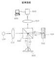
従来の光学式3次元測定装置の一つとして、白色光走査干渉法(WSI:White−light Scanning Interferometry)が提案された。 White light scanning interferometry (WSI) has been proposed as one of the conventional optical three-dimensional measuring apparatuses.
図7を参照すれば、白色光走査干渉法は、光源100から発生し、ビームスプリッタ200で分離された基準光と測定光が基準ミラー400の基準面と測定物300の測定面Pからそれぞれ反射され、相互干渉信号を発生すれば、これを光検出素子500で撮影してから解析する原理を用いる方法であって、基準光と測定光が同一の光経路を通過するときのみに干渉信号が発生する特性を用い、位置検出を通して3次元形状を計測する。 Referring to FIG. 7, in the white light scanning interferometry, the reference light and the measurement light generated from the
このような原理を用いて、PZTアクチュエータなどの移送手段で測定物を光軸方向に微小間隔ずつ移動させながら測定領域内の各測定点での干渉信号を観察すれば、各点の測定光が基準光と同一の光経路を有する地点で短い干渉信号が発生する。 Using this principle, if the interference signal at each measurement point in the measurement region is observed while moving the measurement object in the direction of the optical axis by a transfer means such as a PZT actuator, the measurement light at each point is A short interference signal is generated at a point having the same optical path as the reference light.
したがって、干渉信号の発生位置を測定領域内の全ての測定点で算出すれば、測定面の3次元形状に対する情報を獲得するようになり、獲得された3次元情報から薄膜層の厚さ及び形状を測定することができる。 Therefore, if the generation position of the interference signal is calculated at all measurement points in the measurement region, information about the three-dimensional shape of the measurement surface can be obtained, and the thickness and shape of the thin film layer are obtained from the obtained three-dimensional information. Can be measured.
白色光干渉計測装置は、微細構造物の3次元形状計測だけでなく、誘電体多層膜の膜厚さ測定や、例えば、眼底(eyeground)や皮膚などの連続体(拡散体)の構造解析などにも使用される。 The white light interferometer is not only for measuring the three-dimensional shape of a fine structure, but also for measuring the thickness of a dielectric multilayer film, for example, for analyzing the structure of a continuum (diffuser) such as the eyeground or skin. Also used for.
ところが、従来の形状測定装置は、測定物の寸法を測定する2次元測定装置と測定物の形状及び厚さ(表面粗度)を測定する3次元測定装置がそれぞれ独立的に設計されて別個に使用されるので、測定物の2次元寸法と3次元形状を測定するためには、2次元及び3次元測定装置を交互に使用し、測定物の寸法と形状を測定しなければならないという煩雑さがある。 However, in the conventional shape measuring apparatus, a two-dimensional measuring apparatus for measuring the dimension of the object to be measured and a three-dimensional measuring apparatus for measuring the shape and thickness (surface roughness) of the object to be measured are designed independently. Since it is used, in order to measure the two-dimensional dimension and three-dimensional shape of the measurement object, the two-dimensional and three-dimensional measurement devices must be used alternately to measure the dimension and shape of the measurement object. There is.
また、従来の3次元測定装置を用いる場合、測定物の全体領域に対してスキャンし、干渉縞を得て測定物の欠陥有無を検出することによって、検査速度が遅くなるという短所があった。 In addition, when a conventional three-dimensional measuring apparatus is used, there is a disadvantage that the inspection speed is slowed by scanning the entire area of the measurement object, obtaining interference fringes, and detecting the presence or absence of defects in the measurement object.
本発明の目的は、白色光走査干渉計を用いた表面形状測定において、単一装備を用いて寸法測定と表面欠陥検査に関する2次元情報を獲得し、3次元形状と厚さに関する3次元情報を獲得できるようにする表面形状測定システム及びそれを用いた測定方法を提供することにある。 The object of the present invention is to obtain two-dimensional information related to dimension measurement and surface defect inspection using a single device in surface shape measurement using a white light scanning interferometer, and to obtain three-dimensional information related to three-dimensional shape and thickness. It is an object of the present invention to provide a surface shape measuring system and a measuring method using the same that can be obtained.
また、本発明の他の目的は、白色光走査干渉計を用いた表面形状測定において、単一装備で同軸照明と同軸落射照明を選択的に照射して2次元情報を獲得し、獲得された2次元情報から3次元検査領域を抽出した後、抽出された検査領域のみに対して選択的に3次元測定を行うことによって装備を簡素化し、検査速度を向上できるようにする表面形状測定システム及びそれを用いた測定方法を提供することにある。 Another object of the present invention is to acquire two-dimensional information by selectively irradiating coaxial illumination and coaxial epi-illumination with a single device in surface shape measurement using a white light scanning interferometer. A surface shape measurement system that simplifies the equipment by selectively performing the three-dimensional measurement only on the extracted inspection region after extracting the three-dimensional inspection region from the two-dimensional information, and improves the inspection speed, and It is to provide a measurement method using the same.
前記課題を解決するための本発明の表面形状測定システムは、主光源、集光レンズ及び投影レンズで構成される照明部と、前記照明部からの照明光が基準ミラーの基準面と測定物の測定面にそれぞれ照射されるように照明光を分割するビーム分割器と、前記測定面と前記基準面からそれぞれ反射される基準光と測定光の干渉によって生成された干渉縞を撮影する光検出素子と、前記光検出素子を通して撮像された画像から白色光干渉縞解析を通して表面形状情報を獲得し、獲得された情報を通して欠陥有無を検出する制御コンピュータとを含む表面形状測定システムにおいて、前記測定物とビーム分割器との間には、測定物に対して落射照明を提供する補助光源をさらに備えており、前記主光源と補助光源の点灯及び前記基準面への照明照射を選択的に断続し、表面形状に対する2次元情報及び3次元情報を獲得するものである。 The surface shape measurement system of the present invention for solving the above-described problems includes an illumination unit composed of a main light source, a condenser lens, and a projection lens, and illumination light from the illumination unit is used for the reference surface of the reference mirror and the measurement object. A beam splitter that divides the illumination light so that each of the measurement surfaces is irradiated; and a light detection element that captures interference fringes generated by interference between the measurement light and the reference light reflected from the measurement surface and the reference surface, respectively. A surface shape measurement system comprising: a surface image information obtained through white light interference fringe analysis from an image captured through the light detection element; and a control computer that detects the presence or absence of defects through the obtained information. An auxiliary light source that provides epi-illumination to the object to be measured is further provided between the beam splitter and the main light source and the auxiliary light source. Selectively intermittently, it is to acquire the two-dimensional information and three-dimensional information with respect to the surface shape.
また、前記課題を解決するための本発明の表面形状測定方法は、主光源からの光をそれぞれビーム分割器を用いて基準ミラーの基準面と測定物の測定面に分割して照射し、基準面と測定物の表面からそれぞれ反射される基準光と測定光の干渉によって生成される干渉縞を通して測定物の表面形状を測定する方法において、前記ビーム分割器と測定物との間に補助光源を備えており、前記基準面への照明光の供給を遮断し、前記主光源又は補助光源の点灯を選択的に断続して測定物の2次元情報を獲得する段階と、前記獲得された2次元情報から3次元検査領域を抽出する段階と、前記抽出された検査領域に対する干渉縞を生成し、これを撮像して3次元情報を獲得する段階とを含んで構成される。 Further, in the surface shape measuring method of the present invention for solving the above-mentioned problem, the light from the main light source is irradiated to the reference surface of the reference mirror and the measurement surface of the object to be measured using the beam splitter, respectively, An auxiliary light source is provided between the beam splitter and the measurement object in a method for measuring the surface shape of the measurement object through interference fringes generated by interference between the reference light and the measurement light reflected from the surface and the surface of the measurement object, respectively. Providing the two-dimensional information of the object to be measured by interrupting the supply of illumination light to the reference surface and selectively intermittently turning on the main light source or auxiliary light source; The method includes a step of extracting a three-dimensional inspection region from the information and a step of generating an interference fringe for the extracted inspection region and capturing the three-dimensional information by imaging the interference pattern.
本発明は、測定物に対して同軸照明と落射照明をそれぞれ提供する主光源と補助光源をそれぞれ備えており、各光源の点灯を選択的に断続し、2次元情報を獲得することができ、獲得された情報から3次元検査領域を抽出した後、抽出された検査領域のみに対して3次元検査を行うことによって、単一装備を用いて2次元と3次元情報を全て獲得することができ、装備を簡素化することができる。 The present invention includes a main light source and an auxiliary light source that respectively provide coaxial illumination and epi-illumination to a measurement object, and selectively turns on and off each light source to obtain two-dimensional information. By extracting a 3D inspection area from the acquired information and performing a 3D inspection only on the extracted inspection area, it is possible to acquire both 2D and 3D information using a single equipment. , Equipment can be simplified.
また、本発明は、2次元情報の獲得を先に行い、獲得された2次元情報から3次元検査領域を抽出した後、該当領域のみに対して3次元情報の獲得を行うので、検査速度を向上させることができる。 In the present invention, the acquisition of the two-dimensional information is performed first, and after extracting the three-dimensional inspection area from the acquired two-dimensional information, the three-dimensional information is acquired only for the corresponding area. Can be improved.
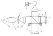
図1は、本発明の表面形状測定システムの装置構成図である。 FIG. 1 is an apparatus configuration diagram of a surface shape measurement system of the present invention.
図1を参照すれば、本発明の表面形状測定システムは、照明部1、ビーム分割器2、光検出素子5及び補助光源7を含んで構成される。 Referring to FIG. 1, the surface shape measurement system of the present invention includes an
ここで、照明部1は、主光源11と、主光源11からの光を集光する集光レンズ12と、集光レンズ12から集光された光をビーム分割器2に投影させる投影レンズ13とを含む。 Here, the
図2は、図1の照明部の他の実施例を示した構成図で、主光源11は、照明パネル11と、照明パネル11にマトリックス状に配列される多数の発光ダイオード111とを含んで構成される。 FIG. 2 is a configuration diagram illustrating another embodiment of the illumination unit of FIG. 1. The
ここで、多数の発光ダイオード111は、中央の発光ダイオード111aを基準にして外郭方向にレイヤ別にグループ化され、グループ別に点灯が制御される。 Here, the multiple
そして、中央の発光ダイオードは、周辺の発光ダイオードの明るさ値より高い明るさ値を有する。 The central light emitting diode has a brightness value higher than that of the peripheral light emitting diodes.
すなわち、2D検査時には、検査領域より大きい同軸照明が必要であるので、発光ダイオード全体を点灯したり、多数のレイヤを点灯して照明を照射する。 That is, during 2D inspection, coaxial illumination larger than the inspection area is necessary, so that the entire light emitting diode is turned on or a number of layers are turned on to illuminate the illumination.
そして、3D検査時には、干渉縞がよく生成される点光源に近い照明を供給するために、中央の発光ダイオード111aのみを点灯することが望ましい。 At the time of 3D inspection, it is desirable to turn on only the central
図3は、図1の照明部の更に他の実施例を示した構成図で、照明部1は、主光源11、集光レンズ12、投影レンズ13及び照明パネル14を含んで構成される。 FIG. 3 is a block diagram showing still another embodiment of the illumination unit in FIG. 1, and the
ここで、照明パネル14には、マトリックス状に配列される多数の発光ダイオード142が備えられ、その中央にピンホール141が形成される。 Here, the
このような構成により、2D検査時には、検査領域より大きい同軸照明が必要であるので、主光源11と照明パネル14の発光ダイオード142全体を点灯したり、発光ダイオード142の多数のレイヤを選択的に点灯することによって照明を照射する。 With such a configuration, during 2D inspection, coaxial illumination larger than the inspection area is required, so the entire
そして、3D検査時には、干渉縞がよく生成される点光源に近い照明を供給するために、主光源11のみを点灯することが望ましい。 At the time of 3D inspection, it is desirable to turn on only the
図4は、図1の照明部の更に他の実施例を示した構成図で、照明部1は、主光源11、顕微鏡対物レンズ12''及び照明パネル14を含む。 FIG. 4 is a block diagram showing still another embodiment of the illumination unit of FIG. 1, and the
ここで、照明パネル14には、マトリックス状に配列される多数の発光ダイオード142が備えられ、その中央にピンホール141が形成される。 Here, the
本発明は、2D検査時、主光源11と照明パネル14にマトリックス状に配列される多数の発光ダイオード142を点灯し、検査領域より広い光を照射する。 In the present invention, at the time of 2D inspection, a large number of
そして、3D検査時、主光源11のみを点灯し、主光源11からの照明光が顕微鏡対物レンズ12'を通過するようにし、その結果、分解能は維持しながら干渉縞の可視度を高めることが望ましい。 At the time of 3D inspection, only the
すなわち、光源の波長が狭いか、レーザソースのように点光源に近いほど、干渉縞がよく生じ、波長が高くなれば分解能が低下するので、光を一点に集める能力に優れた顕微鏡対物レンズ12''を用いることが望ましい。 That is, as the wavelength of the light source is narrower or closer to a point light source such as a laser source, interference fringes occur more frequently, and the resolution decreases as the wavelength increases. Therefore, the microscope
一方、ビーム分割器2は、照明部1からの照明光が基準面Rと測定物の表面Pにそれぞれ照射されるように照明光を分割し、光検出素子5は、干渉縞が形成された画像を撮影する。 On the other hand, the beam splitter 2 divides the illumination light so that the illumination light from the
すなわち、光検出素子5は、基準面Rと測定物の表面Pで反射されたそれぞれの基準光と測定光の干渉によって生成される干渉縞を撮影するもので、投影レンズ13を含む。 That is, the
そして、制御コンピュータ6は、光検出素子5を通して撮像された画像から白色光干渉縞解析を通して表面形状情報を獲得し、獲得された情報分析を通して欠陥有無を検出する。 The control computer 6 acquires surface shape information from the image captured through the
また、補助光源7は、測定物3とビーム分割器2との間に備えられ、測定物3に対して落射照明を提供する。 Further, the auxiliary
ここで、補助光源7は、図5に示すように、リング状本体71と、リング状本体71の内周面に沿って備えられた多数の発光ダイオード72とを含んで構成される。 Here, as shown in FIG. 5, the auxiliary
そして、ビーム分割器2と基準ミラー4との間には、基準面Rへの光照射を選択的に断続する機械的シャッター8がさらに備えられることが望ましい。 It is desirable that a
このような表面形状測定システムは、主光源11の点灯による同軸照明を照査した後、撮影された画像から寸法情報を獲得し、主光源11と補助光源7の点灯による同軸落射照明を照射した後、撮影された画像から表面欠陥情報を獲得することによって、寸法と表面欠陥に関する2次元情報を獲得する。 Such a surface shape measuring system, after checking the coaxial illumination by turning on the main
また、このように獲得された2次元情報を用いて測定物の3次元検査領域を抽出し、抽出された3次元検査領域のみに対して3次元測定を実施する。 Further, the three-dimensional inspection region of the measurement object is extracted using the two-dimensional information acquired in this manner, and the three-dimensional measurement is performed only on the extracted three-dimensional inspection region.
すなわち、抽出された3次元検査領域のみに対して基準光と測定光を形成して干渉縞を生成し、これを撮像して3次元情報を獲得する過程を実施する。 That is, a process of forming reference light and measurement light for only the extracted three-dimensional inspection region to generate interference fringes and capturing the image to acquire three-dimensional information is performed.
以下、本発明の表面形状測定システムを用いた表面形状測定方法を説明する。 Hereinafter, a surface shape measuring method using the surface shape measuring system of the present invention will be described.
まず、主光源11と補助光源7の点灯を選択的に断続し、測定物に対する2次元情報を獲得する。 First, the main
換言すれば、主光源11による同軸照明のみを測定物の表面Pに照射し、測定物の表面Pの映像を光検出素子5で撮影して第1の画像を獲得した後、これを分析して寸法を測定する。
このとき、補助光源7は消灯し、機械的シャッター8を用いて基準面Rへの光の照射を遮断する。In other words, only the coaxial illumination by the main
At this time, the auxiliary
そして、主光源11と補助光源7を同時に点灯して同軸落射照明を照射し、測定物3の表面を光検出素子5で撮影して第2の画像を獲得した後、これを分析して表面欠陥有無を判断する。
このとき、機械的シャッター8を用いて基準面Rへの光の照射を遮断する。Then, the main
At this time, the
このとき、図2〜図4に示すように照明部1が構成された場合、マトリックス状に配列された発光ダイオードがレイヤ別にグループ化されているので、所望の面積又は明るさによって各グループ別発光ダイオードの点灯を選択的に制御することが望ましい。 At this time, when the
このように獲得された測定物の寸法と表面欠陥に対する2次元情報を用いて3次元検査を行うための検査領域を抽出する。 An inspection region for performing a three-dimensional inspection is extracted using the two-dimensional information on the dimension of the measurement object and the surface defect thus obtained.
例えば、図6に示すように、測定物の全体表面に対する2次元情報を獲得し、ここで、“A”領域のように3次元検査が必要な領域を抽出し、該当領域のみに対して基準光と測定光の干渉縞を生成して3次元形状検査を行うことによって、検査速度を向上させる。 For example, as shown in FIG. 6, two-dimensional information on the entire surface of the object to be measured is acquired. Here, an area that requires a three-dimensional inspection, such as the “A” area, is extracted, and the reference is made only for the corresponding area. Inspection speed is improved by generating interference fringes of light and measurement light and performing three-dimensional shape inspection.
ここで、3次元形状検査方法は、基準面Rと測定面Pからそれぞれ反射される基準光と測定光の干渉によって生成された干渉縞を解析する白色光走査干渉を用いる方法であって、以下、これについて簡略に説明する。 Here, the three-dimensional shape inspection method is a method using white light scanning interference for analyzing interference fringes generated by interference between the reference light and the measurement light reflected from the reference surface R and the measurement surface P, respectively. This will be described briefly.
まず、補助光源7は消灯し、主光源11のみを点灯した後、機械的シャッター8を開け、光源11からの光が基準面Rと測定面Pにそれぞれ照射されるようにする。 First, the auxiliary
これによって、基準面Rと測定面Pから反射が起き、基準光と測定光が生成されるので、基準光と測定光の干渉によって生成された干渉縞を光検出素子5で撮影する。 As a result, reflection occurs from the reference surface R and the measurement surface P, and the reference light and the measurement light are generated. Therefore, an interference fringe generated by the interference between the reference light and the measurement light is photographed by the
このとき、基準光と測定光の干渉による干渉縞は、同一の光経路を有するときに生成されるので、図面には具体的に示していないが、PZTアクチュエータなどの微細駆動手段を用いて測定物3の高さ又は基準ミラー4の距離を適切に調節することが望ましい。 At this time, the interference fringes due to the interference between the reference light and the measurement light are generated when they have the same optical path. Therefore, although not specifically shown in the drawing, the measurement is performed using a fine driving means such as a PZT actuator. It is desirable to adjust the height of the
本発明の実施例において、図2に示すように、主光源11をマトリックス状に配列された多数の発光ダイオードで構成した場合、3次元検査時、周辺領域に比べて高い明るさ値を有する中央の発光ダイオードのみを点灯し、干渉縞生成能力を高めることが望ましい。 In the embodiment of the present invention, as shown in FIG. 2, when the main
以上のように、本発明は、測定物に対して同軸照明と落射照明をそれぞれ提供する主光源と補助光源をそれぞれ備えており、各光源の点灯を選択的に断続し、基準面への光照射を遮断して2次元情報を獲得するとともに、獲得された情報から3次元検査領域を抽出した後、抽出された検査領域のみに対して3次元検査を行う。 As described above, the present invention includes the main light source and the auxiliary light source that respectively provide the coaxial illumination and the epi-illumination to the measurement object, and selectively turns on and off the light sources to provide light to the reference surface. The two-dimensional information is acquired by blocking the irradiation, and a three-dimensional inspection region is extracted from the acquired information, and then the three-dimensional inspection is performed only on the extracted inspection region.
1 ・・・ 照明部
2 ・・・ ビーム分割器
3 ・・・ 測定物
4 ・・・ 基準ミラー
5 ・・・ 光検出素子
6 ・・・ 制御コンピュータ
7 ・・・ 補助光源
8 ・・・ 機械的シャッター
11 ・・・ 主光源
11'、143 ・・・ 照明パネル
12 ・・・ 集光レンズ
12' ・・・ 顕微鏡対物レンズ
13 ・・・ 投影レンズ
71 ・・・ リング状本体
72 ・・・ 発光ダイオード
111、111a、132 ・・・ 発光ダイオード
P ・・・ 基準面
R ・・・ 測定物の表面DESCRIPTION OF
Claims (10)
Translated fromJapanese前記測定物(3)に対して落射照明を提供する補助光源(7)が、前記測定物(3)およびビーム分割器(2)間にさらに設けられ、
前記照明部(1)が、前記集光レンズ(12)と投影レンズ(13)との間に備えられているとともに中央にピンホール(141)が形成された照明パネル(14)と、該照明パネル(14)にマトリックス状に配列された多数の発光ダイオード(142)とをさらに含み、
前記主光源(11)と前記補助光源(7)の点灯及び前記基準面(R)への照明照射を選択的に断続し、表面形状に対する2次元情報及び3次元情報を獲得することを特徴とする表面形状測定システム。An illumination unit (1) composed of a main light source (11), a condenser lens (12), and a projection lens (13), and illumination light from the illumination unit (1) is respectively a reference plane ( R) and the beam splitter (2) that divides the illumination light so as to irradiate the measurement surface (P) of the measurement object (3), and are reflected from the measurement surface (P) and the reference surface (R), respectively. A light detection element (5) for photographing an interference fringe generated by the interference between the reference light and the measurement light, and obtaining surface shape information from the image captured through the light detection element (5) through white light interference fringe analysis. A surface shape measurement system including a control computer (6) for detecting the presence or absence of defects through acquired information,
An auxiliary light source (7) that provides epi-illumination for the object to be measured (3) is further provided between the object to be measured (3) and a beam splitter (2),
The illumination unit (1) is provided between the condenser lens (12) and the projection lens (13), and an illumination panel (14) having a pinhole (141) formed in the center thereof, and the illumination A plurality of light emitting diodes (142) arranged in a matrix on the panel (14),
The main light source (11) and the auxiliary light source (7) are turned on and illumination irradiation to the reference surface (R) is selectively interrupted to obtain two-dimensional information and three-dimensional information on the surface shape. Surface shape measurement system.
前記ビーム分割器と前記測定物との間に補助光源を備えており、
前記照明部(1)が、前記集光レンズ(12)と投影レンズ(13)との間に備えられているとともに中央にピンホール(141)が形成された照明パネル(14)と、該照明パネル(14)にマトリックス状に配列された多数の発光ダイオード(142)とをさらに含んでおり、
前記基準面への照明光の供給を遮断し、前記主光源又は補助光源の点灯を選択的に断続して測定物の2次元情報を獲得する段階と、
該獲得された2次元情報から3次元検査領域を抽出する段階と、
該抽出された検査領域に対する干渉縞を生成し、これを撮像して3次元情報を獲得する段階とを含んで構成されていることを特徴とする表面形状測定方法。The light from the main light source is divided into a reference surface of the reference mirror and the measurement surface of the object to be measured using a beam splitter, and the reference light reflected from the reference surface and the measurement surface is interfered with the measurement light, respectively. In the surface shape measuring method for measuring the surface shape of the measurement object through the interference fringes generated by
An auxiliary light source is provided between the beam splitter and the object to be measured;
The illumination unit (1) is provided between the condenser lens (12) and the projection lens (13), and an illumination panel (14) having a pinhole (141) formed in the center thereof, and the illumination A plurality of light emitting diodes (142) arranged in a matrix on the panel (14);
Cutting off the supply of illumination light to the reference plane, selectively turning on or off the main light source or auxiliary light source to obtain two-dimensional information of the measurement object;
Extracting a 3D inspection area from the acquired 2D information;
A method for measuring a surface shape, comprising: generating interference fringes for the extracted inspection region and capturing the three-dimensional information by imaging the interference fringes.
10. The surface shape measuring method according to claim 8, wherein the blocking of the illumination light to the reference surface in the step of acquiring the two-dimensional information is selectively performed through intermittent mechanical shutters.
Applications Claiming Priority (3)
| Application Number | Priority Date | Filing Date | Title |
|---|---|---|---|
| KR10-2007-0131395 | 2007-12-14 | ||
| KR1020070131395AKR100939537B1 (en) | 2007-12-14 | 2007-12-14 | Surface shape measuring system and measuring method using the same |
| PCT/KR2008/007314WO2009078617A2 (en) | 2007-12-14 | 2008-12-10 | Surface shape measuring system and surface shape measuring method using the same |
Publications (2)
| Publication Number | Publication Date |
|---|---|
| JP2011519016A JP2011519016A (en) | 2011-06-30 |
| JP5356402B2true JP5356402B2 (en) | 2013-12-04 |
Family
ID=40795998
Family Applications (1)
| Application Number | Title | Priority Date | Filing Date |
|---|---|---|---|
| JP2010537863AActiveJP5356402B2 (en) | 2007-12-14 | 2008-12-10 | Surface shape measuring system and measuring method using the same |
Country Status (6)
| Country | Link |
|---|---|
| US (1) | US8259305B2 (en) |
| EP (1) | EP2220456B1 (en) |
| JP (1) | JP5356402B2 (en) |
| KR (1) | KR100939537B1 (en) |
| TW (1) | TWI388796B (en) |
| WO (1) | WO2009078617A2 (en) |
Families Citing this family (23)
| Publication number | Priority date | Publication date | Assignee | Title |
|---|---|---|---|---|
| US8432395B2 (en) | 2009-06-16 | 2013-04-30 | Apple Inc. | Method and apparatus for surface contour mapping |
| KR101142763B1 (en)* | 2009-11-04 | 2012-05-18 | 한양대학교 산학협력단 | Spectro reflectometer and method for measuring spectro reflectance using the same |
| CN102822666A (en)* | 2009-11-30 | 2012-12-12 | 株式会社尼康 | Inspection device, three-dimensional shape measuring device, and manufacturing method of structure |
| TWI408331B (en)* | 2009-12-17 | 2013-09-11 | Ind Tech Res Inst | Measurement device and method of double-sided optical films |
| TW201129772A (en)* | 2010-02-26 | 2011-09-01 | Jian-Hong Liu | Measurement system for knife tip and diameter of miniature knife tool |
| JP5721420B2 (en)* | 2010-12-17 | 2015-05-20 | キヤノン株式会社 | Measuring method and measuring device |
| TW201326737A (en)* | 2011-12-30 | 2013-07-01 | Metal Ind Res & Dev Ct | Measuring system and method for morphology of hole surface |
| KR101239409B1 (en)* | 2012-07-12 | 2013-03-05 | 주식회사 엠엠티 | 2d shape and 3d shape measuring apparatus and method based on phase shifting interferometry |
| CN102788558B (en)* | 2012-07-30 | 2014-12-10 | 山东师范大学 | Three-dimensional deformation measuring system and three-dimensional deformation measuring method combining speckle correlation and speckle interference |
| KR101462848B1 (en) | 2013-03-18 | 2014-11-18 | 에스엔유 프리시젼 주식회사 | Three dimensional shape measurment apparatus for recogniting color |
| KR102369792B1 (en) | 2015-03-05 | 2022-03-03 | 한화테크윈 주식회사 | Photographing apparatus and photographing method |
| KR101628761B1 (en)* | 2015-03-06 | 2016-06-09 | (주) 인텍플러스 | surface shape measuring appatstus using asymmetric interferometer |
| KR20170028092A (en)* | 2015-09-03 | 2017-03-13 | 주식회사 이오테크닉스 | Apparatus and method for measuring thickness or height variation of object |
| KR20180007539A (en)* | 2016-07-13 | 2018-01-23 | 주식회사 메디트 | Path Length Multiplier of light for Three dimensional surface measuring |
| CN106441152B (en)* | 2016-10-18 | 2019-02-01 | 淮阴师范学院 | Asymmetric optical interferometry method and device |
| TWI688748B (en)* | 2017-03-30 | 2020-03-21 | 均豪精密工業股份有限公司 | Method of scanning surface profile and apparatus thereof |
| CN108662985B (en)* | 2017-03-30 | 2020-12-11 | 均豪精密工业股份有限公司 | Surface profile scanning method and device |
| CN110514142B (en)* | 2019-09-29 | 2020-09-08 | 中国科学院长春光学精密机械与物理研究所 | Surface shape detection device and surface shape detection method |
| CN113465534B (en)* | 2021-06-25 | 2022-04-19 | 浙江大学 | Micro-nano deep groove structure rapid measurement method based on white light interference |
| KR102660179B1 (en)* | 2021-12-22 | 2024-04-24 | 주식회사 휴비츠 | Calibration method of optical coherence tomography device and camera |
| KR102786771B1 (en)* | 2022-04-22 | 2025-03-31 | 주식회사 카이스 | Inspection apparatus for displacement measurement and visual acquisition at the same time |
| CN116708752B (en)* | 2022-10-28 | 2024-02-27 | 荣耀终端有限公司 | Imaging effect testing method, device and system for imaging device |
| WO2024238875A2 (en)* | 2023-05-18 | 2024-11-21 | Carnegie Mellon University | System and method for swept-angle interferometry |
Family Cites Families (23)
| Publication number | Priority date | Publication date | Assignee | Title |
|---|---|---|---|---|
| JPH0616087B2 (en)* | 1987-09-22 | 1994-03-02 | スタンレー電気株式会社 | Photoelectric detector |
| JP2732123B2 (en)* | 1989-06-19 | 1998-03-25 | 旭光学工業株式会社 | Pattern inspection equipment |
| JPH03209154A (en)* | 1990-01-11 | 1991-09-12 | Narumi China Corp | Automatic appearance checking device |
| JP2974393B2 (en)* | 1990-10-25 | 1999-11-10 | オリンパス光学工業株式会社 | Microscope image input device |
| JPH09250905A (en)* | 1996-01-10 | 1997-09-22 | Olympus Optical Co Ltd | Image measuring optical system |
| JPH109825A (en) | 1996-06-21 | 1998-01-16 | Komatsu Ltd | Confocal optics |
| US5777740A (en)* | 1997-02-27 | 1998-07-07 | Phase Metrics | Combined interferometer/polarimeter |
| JPH10239589A (en)* | 1997-02-28 | 1998-09-11 | Olympus Optical Co Ltd | Interference microscope |
| JPH1194528A (en)* | 1997-09-17 | 1999-04-09 | Nippon Seiko Kk | Appearance inspection device |
| JPH11109253A (en)* | 1997-10-01 | 1999-04-23 | Olympus Optical Co Ltd | Interference microscope |
| JPH11108625A (en)* | 1997-10-06 | 1999-04-23 | Canon Inc | Surface shape measuring device |
| JP3315358B2 (en)* | 1997-12-02 | 2002-08-19 | 株式会社ミツトヨ | Lighting equipment for image processing and measuring machines |
| KR20010101041A (en)* | 1998-11-30 | 2001-11-14 | 기시모토 마사도시 | Measuring instrument |
| JP2002009497A (en)* | 2000-06-23 | 2002-01-11 | Juki Corp | Lighting equipment |
| EP1441215B1 (en)* | 2001-10-31 | 2012-08-01 | Olympus Corporation | Optical scanning type observation device |
| JP2003255256A (en)* | 2002-02-28 | 2003-09-10 | Moritex Corp | Optical scanning device |
| EP1429113A4 (en)* | 2002-08-01 | 2006-06-14 | Asahi Glass Co Ltd | METHOD AND DEVICE FOR INSPECTING CURVED FORMS |
| JP2004077223A (en)* | 2002-08-13 | 2004-03-11 | Nikon Corp | Optical heterodyne interferometer |
| US7095507B1 (en)* | 2002-09-27 | 2006-08-22 | Kla-Tencor Technologies Corporation | Method and apparatus using microscopic and interferometric based detection |
| US7312859B2 (en)* | 2004-01-30 | 2007-12-25 | Promet International, Inc. | Optical fiber inspection device |
| JP2006071353A (en)* | 2004-08-31 | 2006-03-16 | Tokyo Seimitsu Co Ltd | Microscope device, appearance inspection device, semiconductor appearance inspection device, and sample illumination method in microscope device |
| KR100672818B1 (en)* | 2006-01-26 | 2007-01-22 | 주식회사 고영테크놀러지 | 3D shape measurement method |
| DE102006021557B3 (en)* | 2006-05-08 | 2007-07-12 | Carl Mahr Holding Gmbh | Device under test reproducing and/or measuring arrangement for micro system technology, has illumination device illuminating device under test whose light is kept away from reference path |
- 2007
- 2007-12-14KRKR1020070131395Apatent/KR100939537B1/enactiveActive
- 2008
- 2008-12-10USUS12/747,763patent/US8259305B2/enactiveActive
- 2008-12-10TWTW097147944Apatent/TWI388796B/enactive
- 2008-12-10JPJP2010537863Apatent/JP5356402B2/enactiveActive
- 2008-12-10WOPCT/KR2008/007314patent/WO2009078617A2/enactiveApplication Filing
- 2008-12-10EPEP08863179.1Apatent/EP2220456B1/enactiveActive
Also Published As
| Publication number | Publication date |
|---|---|
| TW200930975A (en) | 2009-07-16 |
| US8259305B2 (en) | 2012-09-04 |
| EP2220456B1 (en) | 2019-11-20 |
| WO2009078617A4 (en) | 2009-10-08 |
| TWI388796B (en) | 2013-03-11 |
| US20100259765A1 (en) | 2010-10-14 |
| EP2220456A4 (en) | 2016-08-03 |
| WO2009078617A2 (en) | 2009-06-25 |
| WO2009078617A3 (en) | 2009-08-13 |
| EP2220456A2 (en) | 2010-08-25 |
| KR20090063874A (en) | 2009-06-18 |
| JP2011519016A (en) | 2011-06-30 |
| KR100939537B1 (en) | 2010-02-03 |
Similar Documents
| Publication | Publication Date | Title |
|---|---|---|
| JP5356402B2 (en) | Surface shape measuring system and measuring method using the same | |
| JP6786148B2 (en) | Autofocus system, distance measurement system, autofocus method and autofocus system calibration method | |
| US7852492B2 (en) | Device for tomographic scanning objects | |
| KR102119288B1 (en) | Imaging overlay metrology target and apparatus and method for measuring imaging overlay | |
| JP6446297B2 (en) | Inspection device | |
| TWI402498B (en) | An image forming method and image forming apparatus | |
| JP2013061185A (en) | Pattern inspection device and pattern inspection method | |
| JP7093915B2 (en) | Surface shape measurement method | |
| JP4090860B2 (en) | 3D shape measuring device | |
| JP7667930B2 (en) | Scanning range determination method | |
| KR100785802B1 (en) | Three-dimensional shape measuring device | |
| US20170269482A1 (en) | Inspection Method, Inspection Apparatus and Illumination Method and Apparatus | |
| US9366524B2 (en) | Alignment sensor and height sensor | |
| JP3677444B2 (en) | 3D shape measuring device | |
| KR101764868B1 (en) | Apparatus of high speed white light scanning interferometer using dual coherence for high step height and thickness measurements | |
| JP4464137B2 (en) | Optical 2D and 3D shape measurement system | |
| KR102837207B1 (en) | Apparatus for measuring three-dimensional shape of target object which acquires multiple information of image through a single scan | |
| KR20090068838A (en) | Surface profile inspection device | |
| CN114144662A (en) | Combined transmission and reflected light imaging of internal cracks in semiconductor devices | |
| KR20160095515A (en) | 3 dimensional optical measurement of defect distribution | |
| JP3848586B2 (en) | Surface inspection device | |
| KR102737491B1 (en) | Optical system of an inspection device | |
| JPS62291512A (en) | Distance measuring apparatus | |
| JPH03230544A (en) | Apparatus for inspecting appearance of wafer | |
| US10180315B2 (en) | Apparatus for measuring three-dimensional shape using prism |
Legal Events
| Date | Code | Title | Description |
|---|---|---|---|
| A977 | Report on retrieval | Free format text:JAPANESE INTERMEDIATE CODE: A971007 Effective date:20120217 | |
| A131 | Notification of reasons for refusal | Free format text:JAPANESE INTERMEDIATE CODE: A131 Effective date:20120228 | |
| A521 | Request for written amendment filed | Free format text:JAPANESE INTERMEDIATE CODE: A523 Effective date:20120524 | |
| A131 | Notification of reasons for refusal | Free format text:JAPANESE INTERMEDIATE CODE: A131 Effective date:20130319 | |
| A521 | Request for written amendment filed | Free format text:JAPANESE INTERMEDIATE CODE: A523 Effective date:20130425 | |
| TRDD | Decision of grant or rejection written | ||
| A01 | Written decision to grant a patent or to grant a registration (utility model) | Free format text:JAPANESE INTERMEDIATE CODE: A01 Effective date:20130806 | |
| A61 | First payment of annual fees (during grant procedure) | Free format text:JAPANESE INTERMEDIATE CODE: A61 Effective date:20130828 | |
| R150 | Certificate of patent or registration of utility model | Ref document number:5356402 Country of ref document:JP Free format text:JAPANESE INTERMEDIATE CODE: R150 Free format text:JAPANESE INTERMEDIATE CODE: R150 | |
| R250 | Receipt of annual fees | Free format text:JAPANESE INTERMEDIATE CODE: R250 | |
| R250 | Receipt of annual fees | Free format text:JAPANESE INTERMEDIATE CODE: R250 | |
| R250 | Receipt of annual fees | Free format text:JAPANESE INTERMEDIATE CODE: R250 | |
| R250 | Receipt of annual fees | Free format text:JAPANESE INTERMEDIATE CODE: R250 | |
| R250 | Receipt of annual fees | Free format text:JAPANESE INTERMEDIATE CODE: R250 | |
| R250 | Receipt of annual fees | Free format text:JAPANESE INTERMEDIATE CODE: R250 | |
| R250 | Receipt of annual fees | Free format text:JAPANESE INTERMEDIATE CODE: R250 | |
| R250 | Receipt of annual fees | Free format text:JAPANESE INTERMEDIATE CODE: R250 | |
| R250 | Receipt of annual fees | Free format text:JAPANESE INTERMEDIATE CODE: R250 | |
| R250 | Receipt of annual fees | Free format text:JAPANESE INTERMEDIATE CODE: R250 |