JP5356089B2 - Etching proximity effect correction model creation method, etching proximity effect correction model, mask pattern correction method, photomask, semiconductor device manufacturing method, and semiconductor device - Google Patents
Etching proximity effect correction model creation method, etching proximity effect correction model, mask pattern correction method, photomask, semiconductor device manufacturing method, and semiconductor deviceDownload PDFInfo
- Publication number
- JP5356089B2 JP5356089B2JP2009080348AJP2009080348AJP5356089B2JP 5356089 B2JP5356089 B2JP 5356089B2JP 2009080348 AJP2009080348 AJP 2009080348AJP 2009080348 AJP2009080348 AJP 2009080348AJP 5356089 B2JP5356089 B2JP 5356089B2
- Authority
- JP
- Japan
- Prior art keywords
- pattern
- proximity effect
- etching
- correction model
- effect correction
- Prior art date
- Legal status (The legal status is an assumption and is not a legal conclusion. Google has not performed a legal analysis and makes no representation as to the accuracy of the status listed.)
- Active
Links
Images


Landscapes
- Preparing Plates And Mask In Photomechanical Process (AREA)
- Exposure And Positioning Against Photoresist Photosensitive Materials (AREA)
- Drying Of Semiconductors (AREA)
- Design And Manufacture Of Integrated Circuits (AREA)
Abstract
Description
Translated fromJapanese本発明は、マスクパターンに対しエッチング近接効果補正を行うための補正量を算出するエッチング近接効果補正モデルおよびその作成方法、そのエッチング近接効果補正モデルを用いてマスクパターンを補正するマスクパターンの補正方法、そのエッチング近接効果補正モデルを用いてマスクパターンが補正されたフォトマスク、並びに、そのフォトマスクを用いて配線パターンが形成された半導体装置およびその製造方法に関するものであり、より詳細には、プロセス近接効果による微細パターンの形成精度の低下を改善する技術に関する。 The present invention relates to an etching proximity effect correction model for calculating a correction amount for performing etching proximity effect correction on a mask pattern, a method for creating the same, and a mask pattern correction method for correcting a mask pattern using the etching proximity effect correction model. The present invention relates to a photomask in which a mask pattern is corrected using the etching proximity effect correction model, a semiconductor device in which a wiring pattern is formed using the photomask, and a method of manufacturing the semiconductor device. The present invention relates to a technique for improving a decrease in accuracy of forming a fine pattern due to a proximity effect.
現在、半導体デバイスの高速化や高集積化が進められており、それに伴ってトランジスタや配線パターンの微細化が必要となっている。特にトランジスタの高速化や高集積化に関しては、ゲート寸法の縮小が有効であることが知られている。そこで、現在では、実際に100nm以下の非常に微細なゲート線幅が使用されている。 Currently, semiconductor devices are being increased in speed and integration, and accordingly, transistors and wiring patterns are required to be miniaturized. In particular, it is known that reduction of gate dimensions is effective for increasing the speed and integration of transistors. Therefore, at present, a very fine gate line width of 100 nm or less is actually used.
ゲート線幅のばらつきは、トランジスタの特性および品質に直接影響する。よって、ゲート線幅のばらつきを低減させるために、トランジスタの製造工程におけるリソグラフィー工程において、転写したマスクパターンがシフトしたこと(以下、パターンシフトと略記する)によるパターン間のばらつき(以下、パターン間ばらつきと略記する)を補正する光近接効果補正(Optical Proximity Correction:OPC)技術が、トランジスタ製造分野に既に導入されている。 Variations in gate line width directly affect transistor characteristics and quality. Therefore, in order to reduce the variation in the gate line width, in the lithography process in the transistor manufacturing process, the transferred mask pattern is shifted (hereinafter abbreviated as “pattern shift”). Optical Proximity Correction (OPC) technology is already introduced in the field of transistor manufacturing.
また、トランジスタの製造工程におけるエッチング工程やマスク作製工程において、近接効果により生じたパターンシフトのパターン間ばらつきにより、最終的にウェハ(基板)上に形成した配線パターンにゲート線幅のばらつきが生じることも知られている。これに対しては、近年、上記近接効果により生じるパターンシフトのパターン間ばらつきを補正するプロセス近接効果補正(Process Proximity Correction:PPC)技術が検討されている。 In addition, in the etching process and the mask manufacturing process in the transistor manufacturing process, variations in the pattern of the pattern shift caused by the proximity effect may cause variations in the gate line width in the wiring pattern finally formed on the wafer (substrate). Is also known. In recent years, a process proximity effect correction (Process Proximity Correction: PPC) technique for correcting the pattern shift variation caused by the proximity effect has been studied.
このように、設計寸法通りのゲート線幅を実現するためには、トランジスタ、大きくは半導体装置の製造において、近接効果により生じるパターン間ばらつきを考慮して、マスクパターンの補正を施しておかなければならない。半導体装置の製造におけるマスクパターンの補正方法に関しては、補正のための方法やシステムなどについて様々な提案がされており、例えば、非特許文献1に、エッチング近接効果に対する補正モデルの作成方法について記載されている。 As described above, in order to realize the gate line width as designed, it is necessary to correct the mask pattern in consideration of the pattern-to-pattern variation caused by the proximity effect in the manufacture of a transistor, mainly a semiconductor device. Don't be. As for a mask pattern correction method in the manufacture of a semiconductor device, various proposals have been made regarding correction methods and systems. For example, Non-Patent Document 1 describes a method for creating a correction model for the etching proximity effect. ing.
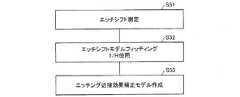
図11は、非特許文献1に記載の、エッチング近接効果に対する補正モデル(以下、エッチング近接効果補正モデルと略記する)の作成フローを示すフローチャートである。 FIG. 11 is a flowchart showing a flow of creating a correction model for the etching proximity effect (hereinafter abbreviated as an etching proximity effect correction model) described in Non-Patent Document 1.
まず、エッチング工程での近接効果を評価するためのマスクパターン(以下、エッチング近接効果評価パターンと略記する)を用いて、エッチング工程の前後のパターン線幅から、エッチング工程におけるパターンシフトであるエッチシフトを測定する(ステップS51)。 First, using a mask pattern for evaluating the proximity effect in the etching process (hereinafter abbreviated as an etching proximity effect evaluation pattern), an etch shift, which is a pattern shift in the etching process, from the pattern line width before and after the etching process. Is measured (step S51).
続いて、エッチング近接効果評価パターンを用いて算出したエッチシフトに対して、パターンの密度(以下、パターン密度と略記する)と、パターン間のスペース(以下、パターン間スペースと略記する)の関数とをパラメータとする補正モデルを用いて、最小二乗法によるフィッティングを行う(ステップS52)。このフィッティングの際には、補正モデルにはパターン間スペースの関数をRとした場合の関数1/Rを用いて、パターン密度の係数、およびパターン間スペースの関数の係数をそれぞれ算出する。 Subsequently, with respect to the etch shift calculated using the etching proximity effect evaluation pattern, a function of pattern density (hereinafter abbreviated as pattern density) and a space between patterns (hereinafter abbreviated as inter-pattern space) Fitting by the least squares method is performed using a correction model having as a parameter (step S52). In this fitting, the function 1 / R where the inter-pattern space function is R is used as the correction model, and the pattern density coefficient and the inter-pattern space function coefficient are calculated.
これにより、エッチング近接効果補正モデルを作成する(ステップS53)。このエッチング近接効果補正モデルと、実際のエッチング近接効果により生じたエッチシフトを測定したときの実測値との間の関係を、図12(a)(b)に示す。 Thereby, an etching proximity effect correction model is created (step S53). FIGS. 12A and 12B show the relationship between this etching proximity effect correction model and the actually measured value when the etch shift caused by the actual etching proximity effect is measured.
図12(a)は、エッチング近接効果補正モデルにおける、パターン間スペースの値に対してのエッチシフトの値(グラフ中の四角のポイント)と、パターン間スペースの値に対してのエッチシフトの実測値(グラフ中の丸のポイント)とを示している。また、横軸はパターン間スペースの幅(nm)を示し、縦軸はエッチシフト(nm)を示している。 FIG. 12A shows an etch shift value (square point in the graph) with respect to the inter-pattern space value and an actual measurement of the etch shift with respect to the inter-pattern space value in the etching proximity effect correction model. Values (circle points in the graph). The horizontal axis indicates the width (nm) of the inter-pattern space, and the vertical axis indicates the etch shift (nm).
図12(b)は、図12(a)に示したような、エッチング近接効果補正モデルにおけるエッチシフトの値を、エッチシフトの実測値にフィッティングした結果を示している。横軸はパターン間スペースの幅(nm)を示し、縦軸は、フィッティングしたときの残差(モデルフィッティング残差)(nm)を示している。 FIG. 12B shows the result of fitting the etch shift value in the etching proximity effect correction model as shown in FIG. 12A to the measured value of the etch shift. The horizontal axis indicates the width (nm) of the space between patterns, and the vertical axis indicates the residual when fitting (model fitting residual) (nm).
このように、非特許文献1に記載の技術では、図12(b)に示すようなフィッティング結果を有するエッチング近接効果補正モデルを作成することが可能である。このエッチング近接効果補正モデルを用いて補正を行ったマスクパターンを有するマスクを作製し、このマスクを用いてエッチングを行うことにより、設計寸法に近づくようなゲート線幅を持つ配線パターンを実現することが可能となる。 As described above, with the technique described in Non-Patent Document 1, it is possible to create an etching proximity effect correction model having a fitting result as shown in FIG. Create a mask having a mask pattern corrected using this etching proximity effect correction model, and perform etching using this mask to realize a wiring pattern having a gate line width that approaches the design dimension. Is possible.
しかしながら、上述したエッチング近接効果補正モデルでは、図12(b)に示すように、パターン間スペースの幅が0.2μm未満の狭いスペース領域(グラフ中のX)、0.2μm〜2μmの中間スペース領域(グラフ中のY)、および、5μm以上の広いスペース領域(グラフ中のZ)において、5nmを超えるモデルフィッティング残差が残っている。これは、図12(a)に示す、スペース領域x、yおよびzにおけるエッチング近接効果補正モデルの精度が高くないためである。 However, in the etching proximity effect correction model described above, as shown in FIG. 12B, a narrow space region (X in the graph) where the width of the space between patterns is less than 0.2 μm, and an intermediate space of 0.2 μm to 2 μm. In the region (Y in the graph) and the wide space region (Z in the graph) of 5 μm or more, the model fitting residual exceeding 5 nm remains. This is because the accuracy of the etching proximity effect correction model in the space regions x, y, and z shown in FIG.
このため、非特許文献1に記載の技術では、高精度のエッチング近接効果補正モデルを作成することが不可能である。それゆえ、半導体装置の基板上に形成される最終的な配線パターンの寸法を、設計寸法通りに精度良く形成することができないという問題点を有している。 For this reason, with the technique described in Non-Patent Document 1, it is impossible to create a highly accurate etching proximity effect correction model. Therefore, there is a problem that the dimensions of the final wiring pattern formed on the substrate of the semiconductor device cannot be accurately formed as designed.
本発明は、上記従来の問題点に鑑みなされたものであって、その目的は、非常に高精度のエッチング近接効果補正モデルを作成することができるエッチング近接効果補正モデルの作成方法、エッチング近接効果補正モデル、そのエッチング近接効果補正モデルを用いてエッチング近接効果に対するマスクパターンの補正を非常に高精度で行うことができるマスクパターンの補正方法、フォトマスク、半導体装置の製造方法、並びに半導体装置を提供することにある。 The present invention has been made in view of the above-described conventional problems, and an object of the present invention is to create an etching proximity effect correction model that can create an etching proximity effect correction model with very high accuracy, an etching proximity effect, and the like. Provided are a correction model, a mask pattern correction method, a photomask, a method for manufacturing a semiconductor device, and a semiconductor device capable of correcting the mask pattern for the etching proximity effect with very high accuracy using the correction model for the etching proximity effect There is to do.
本発明のエッチング近接効果補正モデルの作成方法は、上記課題を解決するために、マスクパターンに対しエッチング近接効果補正を行うための補正量を算出するエッチング近接効果補正モデルを作成する方法であって、基板の配線形成面にレジストを形成し、評価用パターンを搭載した評価用フォトマスクを用いて該レジストにリソグラフィー処理を行うことにより、評価用パターンが転写されたレジストパターンを形成するステップと、上記レジストパターンに対し、リソグラフィー近接効果補正モデルを用いてシミュレーションを行うことにより、該レジストパターンの線幅のシミュレーション値を算出するステップと、上記レジストパターンをマスクとして上記基板の配線形成面をエッチングすることにより、配線パターンを形成するステップと、上記配線パターンの線幅を測定するステップと、上記レジストパターンの線幅のシミュレーション値と、上記配線パターンの線幅の実測値とから、上記エッチングによるパターンのシフト量を算出するステップと、上記シフト量に対し、パターンサイズおよびパターン間スペースサイズをパラメータとする補正モデルを用いて、最小二乗法によるフィッティングを行うことにより、エッチング近接効果補正モデルを作成するステップと、を含むことを特徴としている。 An etching proximity effect correction model creation method of the present invention is a method of creating an etching proximity effect correction model for calculating a correction amount for performing etching proximity effect correction on a mask pattern in order to solve the above-described problem. Forming a resist pattern on which the evaluation pattern is transferred by forming a resist on the wiring formation surface of the substrate and performing a lithography process on the resist using a photomask for evaluation mounted with the evaluation pattern; A simulation is performed on the resist pattern using a lithography proximity effect correction model to calculate a simulation value of the line width of the resist pattern, and a wiring formation surface of the substrate is etched using the resist pattern as a mask. Form a wiring pattern A step of measuring a line width of the wiring pattern; a step of calculating a shift amount of the pattern by the etching from a simulation value of the line width of the resist pattern and an actual measurement value of the line width of the wiring pattern; A step of creating an etching proximity effect correction model by performing fitting by a least square method using a correction model with the pattern size and the inter-pattern space size as parameters for the shift amount. It is said.
上記の方法によれば、エッチング近接効果補正モデルを作成するためにフィッティングを行う際に用いるシフト量は、リソグラフィー近接効果補正モデルを用いてシミュレーションを行うことにより算出したレジストパターンの線幅のシミュレーション値を用いて算出している。それゆえ、リソグラフィー近接効果補正モデルに誤差がある場合、この誤差がシフト量の中に含まれるので、誤差を考慮したフィッティングを行うことになる。 According to the above method, the shift amount used when fitting to create the etching proximity effect correction model is the simulation value of the line width of the resist pattern calculated by performing the simulation using the lithography proximity effect correction model. It is calculated using. Therefore, if there is an error in the lithography proximity effect correction model, this error is included in the shift amount, and therefore fitting considering the error is performed.
よって、リソグラフィー近接効果補正モデルの誤差を吸収したエッチング近接効果補正モデルを作成することが可能となり、パターン補正精度をさらに向上することが可能となる。また、エッチング近接効果補正モデルは、パターンサイズおよびパターン間スペースサイズで定義されるので、精度良く作成される。したがって、非常に高精度のエッチング近接効果補正モデルを作成することが可能となる。 Therefore, it is possible to create an etching proximity effect correction model that absorbs errors in the lithography proximity effect correction model, and it is possible to further improve the pattern correction accuracy. Further, the etching proximity effect correction model is defined by the pattern size and the inter-pattern space size, and thus is created with high accuracy. Therefore, it is possible to create a highly accurate etching proximity effect correction model.
また、本発明のエッチング近接効果補正モデルの作成方法は、上記の問題を解決するために、上記補正モデルは、上記パターン間スペースサイズのパラメータをRとする場合、関数R−n(n:正の実数)および対数関数Log(R)が線形結合された式を少なくとも含んでいることを特徴としている。Further,in order to solve the above problem , the method for creating an etching proximity effect correction model of the present invention has a function R−n (n: positive) when the parameter of the inter-pattern space size is R. real number) and logarithmic function Log (R)is characterized in that it comprises at least a linear combination expression.
上記の構成によれば、関数R−nは、例えば、レジスト下部形状による依存性を含めた、フォトレジストの下層に設けられる有機反射防止膜をエッチングする際のパターン依存性を良く再現し、また、対数関数Log(R)は、配線パターンの材料、例えば、多結晶シリコンを、エッチングする際のパターン依存性を良く再現する。これにより、エッチング近接効果補正モデルの精度をさらに向上させることが可能となる。According to the above configuration, the function R−n well reproduces the pattern dependency when etching the organic antireflection film provided in the lower layer of the photoresist, including the dependency due to the resist lower shape, for example. The logarithmic function Log (R) reproduces well the pattern dependency when etching a material of a wiring pattern, for example, polycrystalline silicon. Thereby, the accuracy of the etching proximity effect correction model can be further improved.
なお、特に、関数R−1は、フォトレジストの下層に設けられる有機反射防止膜をエッチングする際のパターン依存性を、関数R−2は、エッチングによりパターンがシフトする際の、レジストパターンのレジスト下部形状による依存性を、非常に良く再現する。それゆえ、本発明のエッチング近接効果補正モデルの作成方法は、上記関数R−nは、1≦n≦2の範囲で設定されることが望ましい。In particular, the function R-1 is the pattern dependency when etching the organic antireflection film provided in the lower layer of the photoresist, and the function R-2 is the resist pattern resist when the pattern is shifted by etching. The dependency due to the lower shape is reproduced very well. Therefore, in the method for creating the etching proximity effect correction model of the present invention, it is desirable that the function R−n is set in the range of 1 ≦ n ≦ 2.
また、本発明のエッチング近接効果補正モデルの作成方法は、上記評価用パターンでは、一定のパターンピッチを有する繰り返しパターンが定められていることが好ましい。 In the method for creating an etching proximity effect correction model of the present invention, it is preferable that a repetitive pattern having a constant pattern pitch is defined in the evaluation pattern.
上記の構成によれば、パターンサイズおよびパターン間スペースサイズのパラメータを容易に抽出することが可能となり、パターンサイズおよびパターン間スペースサイズをパラメータとして用いることによるモデル化を容易に行うことが可能となる。 According to the above configuration, it is possible to easily extract the parameters of the pattern size and the inter-pattern space size, and it is possible to easily perform modeling by using the pattern size and the inter-pattern space size as parameters. .
本発明のエッチング近接効果補正モデルは、マスクパターンに対しエッチング近接効果補正を行うための補正量を算出するエッチング近接効果補正モデルであって、基板の配線形成面に形成されたレジストパターンに対しリソグラフィー近接効果補正モデルを用いてシミュレーションを行うことにより算出された、該レジストパターンの線幅のシミュレーション値と、上記レジストパターンをマスクとして上記基板の配線形成面をエッチングすることにより形成された配線パターンの線幅の実測値と、から算出された上記エッチングによるパターンのシフト量に対し、パターンサイズおよびパターン間スペースサイズをパラメータとする補正モデルを用いて、最小二乗法によるフィッティングを行うことにより作成されていることを特徴としている。 The etching proximity effect correction model of the present invention is an etching proximity effect correction model for calculating a correction amount for performing an etching proximity effect correction on a mask pattern, and lithography is performed on a resist pattern formed on a wiring formation surface of a substrate. A simulation value of the line width of the resist pattern calculated by performing a simulation using a proximity effect correction model, and a wiring pattern formed by etching the wiring formation surface of the substrate using the resist pattern as a mask. It is created by fitting the measured value of the line width and the pattern shift amount calculated from the above using the correction model with the pattern size and the inter-pattern space size as parameters, using the least square method. It is characterized by There.
上記の構成によれば、エッチング近接効果補正モデルを作成するためにフィッティングを行う際に用いられるシフト量は、リソグラフィー近接効果補正モデルを用いてシミュレーションを行うことにより算出された、レジストパターンの線幅のシミュレーション値を用いて算出されている。それゆえ、リソグラフィー近接効果補正モデルに誤差がある場合、この誤差がシフト量の中に含まれるので、誤差を考慮したフィッティングが行われることになる。 According to the above configuration, the shift amount used when fitting to create the etching proximity effect correction model is the line width of the resist pattern calculated by performing a simulation using the lithography proximity effect correction model. It is calculated using the simulation value. Therefore, if there is an error in the lithography proximity effect correction model, this error is included in the shift amount, and therefore fitting considering the error is performed.
よって、リソグラフィー近接効果補正モデルの誤差を吸収したエッチング近接効果補正モデルを作成することが可能となり、パターン補正精度をさらに向上することが可能となる。また、エッチング近接効果補正モデルは、パターンサイズおよびパターン間スペースサイズで定義されるので、精度良く作成される。したがって、非常に高精度のエッチング近接効果補正モデルを作成することが可能となる。 Therefore, it is possible to create an etching proximity effect correction model that absorbs errors in the lithography proximity effect correction model, and it is possible to further improve the pattern correction accuracy. Further, the etching proximity effect correction model is defined by the pattern size and the inter-pattern space size, and thus is created with high accuracy. Therefore, it is possible to create a highly accurate etching proximity effect correction model.
また、本発明のエッチング近接効果補正モデルは、上記の問題を解決するために、上記補正モデルは、上記パターン間スペースサイズのパラメータをRとする場合、関数R−n(n:正の実数)および対数関数Log(R)が線形結合された式を少なくとも含んでいることを特徴としている。Further, the etching proximity effect correction model of the present inventionsolves the above-mentioned problem. In the correction model, when the parameter of the inter-pattern space size is R, the function R−n (n: positive real number) andit is characterized by a logarithmic function Log (R) contains at least a linear combination expression.
上記の構成によれば、関数R−nは、例えば、レジスト下部形状による依存性を含めた、フォトレジストの下層に設けられる有機反射防止膜をエッチングする際のパターン依存性を良く再現し、また、対数関数Log(R)は、配線パターンの材料、例えば、多結晶シリコンを、エッチングする際のパターン依存性を良く再現する。これにより、エッチング近接効果補正モデルの精度をさらに向上させることが可能となる。According to the above configuration, the function R−n well reproduces the pattern dependency when etching the organic antireflection film provided in the lower layer of the photoresist, including the dependency due to the resist lower shape, for example. The logarithmic function Log (R) reproduces well the pattern dependency when etching a material of a wiring pattern, for example, polycrystalline silicon. Thereby, the accuracy of the etching proximity effect correction model can be further improved.
なお、特に、関数R−1は、フォトレジストの下層に設けられる有機反射防止膜をエッチングする際のパターン依存性を、関数R−2は、エッチングによりパターンがシフトする際の、レジストパターンのレジスト下部形状による依存性を、非常に良く再現する。それゆえ、本発明のエッチング近接効果補正モデルは、上記関数R−nは、1≦n≦2の範囲で設定されることが望ましい。In particular, the function R-1 is the pattern dependency when etching the organic antireflection film provided in the lower layer of the photoresist, and the function R-2 is the resist pattern resist when the pattern is shifted by etching. The dependency due to the lower shape is reproduced very well. Therefore, in the etching proximity effect correction model of the present invention, it is desirable that the function R−n is set in the range of 1 ≦ n ≦ 2.
本発明のマスクパターンの補正方法は、マスクのマスクパターンを、該マスクを用いた微細加工プロセスによって所望の寸法を持つ配線パターンが形成されるように補正する方法であって、上記微細加工プロセスを実施する前に、エッチング近接効果に対する上記マスクパターンの補正を、上記エッチング近接効果補正モデルを用いて行うことを特徴としている。 A mask pattern correction method according to the present invention is a method for correcting a mask pattern of a mask so that a wiring pattern having a desired dimension is formed by a fine processing process using the mask. Before implementation, the mask pattern correction for the etching proximity effect is performed using the etching proximity effect correction model.
上記の方法によれば、微細加工プロセスを実施する前に、微細加工プロセスにて用いるマスクのマスクパターンに、非常に高精度のエッチング近接効果補正モデルを用いてエッチング近接効果に対する補正を行う。よって、エッチング近接効果に対するマスクパターンの補正を非常に高精度で行うことが可能となり、設計寸法に非常に近づく配線パターンの形成につなげることが可能となる。 According to the above method, before performing the microfabrication process, the mask proximity pattern of the mask used in the microfabrication process is corrected for the etching proximity effect using an extremely accurate etching proximity effect correction model. Therefore, it is possible to correct the mask pattern with respect to the etching proximity effect with very high accuracy, and to lead to formation of a wiring pattern that is very close to the design dimension.
また、本発明のマスクパターンの補正方法は、上記エッチング近接効果補正モデルを用いて、1次元の上記パターンサイズおよびパターン間スペースサイズの組合せにより算出した補正量を規定した補正ルールを作成し、該補正ルールを用いて、上記エッチング近接効果に対する上記マスクパターンの補正を行うことが好ましい。 Further, the mask pattern correction method of the present invention creates a correction rule that defines a correction amount calculated by a combination of the one-dimensional pattern size and the inter-pattern space size using the etching proximity effect correction model. It is preferable to correct the mask pattern with respect to the etching proximity effect using a correction rule.
上記の方法によれば、補正処理の際に、1次元(例えば、横方向)のみのパターンサイズおよびパターン間スペースサイズを検出すればよいため、補正処理にかかる時間を短縮することが可能となる。 According to the above method, since it is only necessary to detect a one-dimensional (for example, horizontal direction) pattern size and an inter-pattern space size during the correction process, it is possible to reduce the time required for the correction process. .
本発明のフォトマスクは、上記エッチング近接効果補正モデルが用いられることによって、エッチング近接効果に対する補正が行われたマスクパターンを有することを特徴としている。 The photomask of the present invention has a mask pattern in which the etching proximity effect is corrected by using the etching proximity effect correction model.
上記の構成によれば、非常に高精度のエッチング近接効果補正モデルを用いることから、所望の寸法を持つ配線パターンが基板上に形成されるように、エッチング近接効果に対する補正が非常に高精度で行われたマスクパターンを有するフォトマスクを実現することが可能となる。 According to the above configuration, since the etching proximity effect correction model having a very high accuracy is used, the correction for the etching proximity effect can be performed with a very high accuracy so that a wiring pattern having a desired dimension is formed on the substrate. It is possible to realize a photomask having a mask pattern that has been performed.
本発明の半導体装置の製造方法は、マスクを用いた微細加工プロセスにより形成された配線パターンを備えている半導体装置を製造する方法であって、マスクパターンのデータに対し、少なくとも、上記エッチング近接効果補正モデルを用いてエッチング近接効果に対する補正、およびリソグラフィー近接効果補正モデルを用いてリソグラフィー近接効果に対する補正を含む補正を行うステップと、上記補正を行ったマスクパターンのデータに基づいてマスクを作成するステップと、上記作成したマスクを用いて、微細加工プロセスにより配線パターンを形成する工程と、を含むことを特徴としている。 A method of manufacturing a semiconductor device according to the present invention is a method of manufacturing a semiconductor device having a wiring pattern formed by a microfabrication process using a mask, and at least the etching proximity effect on mask pattern data. Performing correction including correction for etching proximity effect using the correction model, and correction for lithography proximity effect using the lithography proximity effect correction model, and creating a mask based on the mask pattern data subjected to the correction And a step of forming a wiring pattern by a microfabrication process using the created mask.
上記の方法によれば、リソグラフィー近接効果補正モデルの誤差を吸収する非常に高精度のエッチング近接効果補正モデルを用いて、エッチング近接効果に対する補正が行われたマスクパターンを有するマスクが作成され、このマスクを用いて配線パターンが形成される。よって、リソグラフィー近接効果補正モデルに誤差がある場合であっても、所望の寸法を持つ配線パターンを非常に高精度で形成することが可能となる。 According to the above method, a mask having a mask pattern in which correction for the etching proximity effect is performed is created using a highly accurate etching proximity effect correction model that absorbs an error of the lithography proximity effect correction model. A wiring pattern is formed using the mask. Therefore, even when there is an error in the lithography proximity effect correction model, a wiring pattern having a desired dimension can be formed with very high accuracy.
本発明の半導体装置は、上記エッチング近接効果補正モデルを用いてエッチング近接効果に対する補正が行われたマスクパターン、を有するマスクを用いた微細加工プロセスにより形成された配線パターンを備えていることを特徴としている。 A semiconductor device according to the present invention includes a wiring pattern formed by a microfabrication process using a mask having a mask pattern corrected for the etching proximity effect using the etching proximity effect correction model. It is said.
上記の構成によれば、非常に高精度のエッチング近接効果補正モデルを用いることから、マスクのマスクパターンは、エッチング近接効果に対する補正が非常に高精度で行われている。よって、所望の寸法を持つ配線パターンが非常に高精度で形成された半導体装置を実現することが可能となる。 According to the above configuration, since the etching proximity effect correction model with very high accuracy is used, the mask pattern of the mask is corrected with respect to the etching proximity effect with very high accuracy. Therefore, it is possible to realize a semiconductor device in which a wiring pattern having a desired dimension is formed with very high accuracy.
以上のように、本発明のエッチング近接効果補正モデルの作成方法は、基板の配線形成面にレジストを形成し、評価用パターンを搭載した評価用フォトマスクを用いて該レジストにリソグラフィー処理を行うことにより、評価用パターンが転写されたレジストパターンを形成するステップと、上記レジストパターンに対し、リソグラフィー近接効果補正モデルを用いてシミュレーションを行うことにより、該レジストパターンの線幅のシミュレーション値を算出するステップと、上記レジストパターンをマスクとして上記基板の配線形成面をエッチングすることにより、配線パターンを形成するステップと、上記配線パターンの線幅を測定するステップと、上記レジストパターンの線幅のシミュレーション値と、上記配線パターンの線幅の実測値とから、上記エッチングによるパターンのシフト量を算出するステップと、上記シフト量に対し、パターンサイズおよびパターン間スペースサイズをパラメータとする補正モデルを用いて、最小二乗法によるフィッティングを行うことにより、エッチング近接効果補正モデルを作成するステップと、を含み、上記補正モデルは、上記パターン間スペースサイズのパラメータをRとする場合、関数R−n(n:正の実数)および対数関数Log(R)が線形結合された式を少なくとも含んでいる方法である。As described above, the etching proximity effect correction model creation method of the present invention includes forming a resist on the wiring formation surface of the substrate, and performing lithography processing on the resist using the evaluation photomask on which the evaluation pattern is mounted. A step of forming a resist pattern to which the evaluation pattern is transferred, and a step of calculating a simulation value of the line width of the resist pattern by performing a simulation on the resist pattern using a lithography proximity effect correction model Etching a wiring forming surface of the substrate using the resist pattern as a mask, measuring a line width of the wiring pattern, a simulation value of the line width of the resist pattern, The actual line width of the above wiring pattern By calculating the pattern shift amount due to the etching from the value, and using the correction model with the pattern size and the inter-pattern space size as parameters for the shift amount, by performing the fitting by the least square method,viewed contains a step of creating an etching proximity effect correction model,and the correction model, when the parameters of the space size between the patterns and R, the function R-n(n:a positive real number) and logarithmic function Log (R ) Includes at least linearly combined expressions .
また、本発明のエッチング近接効果補正モデルは、基板の配線形成面に形成されたレジストパターンに対しリソグラフィー近接効果補正モデルを用いてシミュレーションを行うことにより算出された、該レジストパターンの線幅のシミュレーション値と、上記レジストパターンをマスクとして上記基板の配線形成面をエッチングすることにより形成された配線パターンの線幅の実測値と、から算出された上記エッチングによるパターンのシフト量に対し、パターンサイズおよびパターン間スペースサイズをパラメータとする補正モデルを用いて、最小二乗法によるフィッティングを行うことにより作成されており、上記補正モデルは、上記パターン間スペースサイズのパラメータをRとする場合、関数R−n(n:正の実数)および対数関数Log(R)が線形結合された式を少なくとも含んでいる構成である。Further, the etching proximity effect correction model of the present invention is a simulation of the line width of the resist pattern calculated by simulating the resist pattern formed on the wiring forming surface of the substrate using the lithography proximity effect correction model. The pattern size and the shift amount of the pattern by the etching calculated from the value and the measured value of the line width of the wiring pattern formed by etching the wiring forming surface of the substrate using the resist pattern as a mask.The correction model is created by performing the fitting by the least square method using a correction model having an inter-pattern space size as a parameter. The correction model has a function R−nwhen the inter-pattern space size parameter is R.(N: positive real number) and logarithmic function Log (R) is atleast comprise and constitutea linear combination expression.
それゆえ、リソグラフィー近接効果補正モデルの誤差を吸収したエッチング近接効果補正モデルを作成することが可能となり、パターン補正精度をさらに向上することが可能となる。また、エッチング近接効果補正モデルは、パターンサイズおよびパターン間スペースサイズで定義されるので、精度良く作成される。したがって、非常に高精度のエッチング近接効果補正モデルを作成することができるという効果を奏する。 Therefore, it is possible to create an etching proximity effect correction model that absorbs errors in the lithography proximity effect correction model, and it is possible to further improve the pattern correction accuracy. Further, the etching proximity effect correction model is defined by the pattern size and the inter-pattern space size, and thus is created with high accuracy. Therefore, it is possible to create an extremely accurate etching proximity effect correction model.
本発明のマスクパターンの補正方法は、微細加工プロセスを実施する前に、エッチング近接効果に対するマスクパターンの補正を、上記エッチング近接効果補正モデルを用いて行う方法であるので、微細加工プロセスにて用いるマスクのマスクパターンに、非常に高精度のエッチング近接効果補正モデルを用いてエッチング近接効果に対する補正を行う。よって、エッチング近接効果に対するマスクパターンの補正を非常に高精度で行うことが可能となり、設計寸法に非常に近づく配線パターンの形成につなげることができるという効果を奏する。 The mask pattern correction method according to the present invention is a method in which the mask pattern correction for the etching proximity effect is performed using the etching proximity effect correction model before the fine processing process is performed. Etching proximity effect correction is performed on the mask pattern of the mask using an extremely accurate etching proximity effect correction model. Therefore, it is possible to correct the mask pattern with respect to the etching proximity effect with very high accuracy, and there is an effect that it can be connected to formation of a wiring pattern that is very close to the design dimension.
本発明のフォトマスクは、上記エッチング近接効果補正モデルが用いられることによって、エッチング近接効果に対する補正が行われたマスクパターンを有する構成であるので、非常に高精度のエッチング近接効果補正モデルを用いることから、所望の寸法を持つ配線パターンが基板上に形成されるように、エッチング近接効果に対する補正が非常に高精度で行われたマスクパターンを有することができるという効果を奏する。 Since the photomask of the present invention has a mask pattern in which the etching proximity effect correction is performed by using the etching proximity effect correction model, a highly accurate etching proximity effect correction model is used. Therefore, the mask pattern in which correction for the etching proximity effect is performed with very high accuracy can be provided so that a wiring pattern having a desired dimension is formed on the substrate.
本発明の半導体装置の製造方法は、マスクパターンのデータに対し、少なくとも、上記エッチング近接効果補正モデルを用いてエッチング近接効果に対する補正、およびリソグラフィー近接効果補正モデルを用いてリソグラフィー近接効果に対する補正を含む補正を行うステップと、上記補正を行ったマスクパターンのデータに基づいてマスクを作成するステップと、上記作成したマスクを用いて、微細加工プロセスにより配線パターンを形成する工程と、を含む方法であるので、リソグラフィー近接効果補正モデルの誤差を吸収する非常に高精度のエッチング近接効果補正モデルを用いて、エッチング近接効果に対する補正が行われたマスクパターンを有するマスクが作成され、このマスクを用いて配線パターンが形成される。よって、リソグラフィー近接効果補正モデルに誤差がある場合であっても、所望の寸法を持つ配線パターンを非常に高精度で形成することができるという効果を奏する。 The method for manufacturing a semiconductor device of the present invention includes at least correction for the etching proximity effect using the etching proximity effect correction model and correction for the lithography proximity effect using the lithography proximity effect correction model for mask pattern data. The method includes a step of performing correction, a step of creating a mask based on the data of the mask pattern subjected to the correction, and a step of forming a wiring pattern by a microfabrication process using the created mask. Therefore, a mask having a mask pattern in which the correction for the etching proximity effect is corrected is created by using the etching proximity effect correction model with very high accuracy that absorbs the error of the lithography proximity effect correction model, and wiring is performed using this mask. A pattern is formed. Therefore, even if there is an error in the lithography proximity effect correction model, there is an effect that a wiring pattern having a desired dimension can be formed with very high accuracy.
本発明の半導体装置は、上記エッチング近接効果補正モデルを用いてエッチング近接効果に対する補正が行われたマスクパターン、を有するマスクを用いた微細加工プロセスにより形成された配線パターンを備えている構成であるので、非常に高精度のエッチング近接効果補正モデルを用いることから、マスクのマスクパターンは、エッチング近接効果に対する補正が非常に高精度で行われている。よって、所望の寸法を持つ配線パターンが非常に高精度で形成された半導体装置を実現することができるという効果を奏する。 A semiconductor device according to the present invention includes a wiring pattern formed by a microfabrication process using a mask having a mask pattern corrected for the etching proximity effect using the etching proximity effect correction model. Therefore, since the etching proximity effect correction model with very high accuracy is used, the mask pattern of the mask is corrected with respect to the etching proximity effect with very high accuracy. Therefore, it is possible to realize a semiconductor device in which a wiring pattern having a desired dimension is formed with very high accuracy.
本発明に係るエッチング近接効果補正モデルの作成方法は、非常に高精度のエッチング近接効果補正モデルを作成することができる方法である。そして、このエッチング近接効果補正モデルを用いるマスクパターンの補正では、最終的に所望の寸法を持つ配線パターンが基板上に形成されるように、エッチング近接効果に対するマスクパターンの補正を非常に高精度で行うことができる。 The method for creating an etching proximity effect correction model according to the present invention is a method capable of creating an etching proximity effect correction model with very high accuracy. In the mask pattern correction using this etching proximity effect correction model, the mask pattern correction with respect to the etching proximity effect is performed with very high accuracy so that a wiring pattern having a desired dimension is finally formed on the substrate. It can be carried out.
以下では、まず、本発明のエッチング近接効果補正モデルの作成方法の比較例について説明し、その次に、そのエッチング近接効果補正モデルを用いてマスクパターンの補正を行うエッチング近接効果補正工程を含む半導体装置の製造方法について説明する。そしてその次に、本発明のエッチング近接効果補正モデルの作成方法について説明する。 In the following, first, a comparative example of a method for creating an etching proximity effect correction model of the present invention will be described, and then a semiconductor including an etching proximity effect correction process for correcting a mask pattern using the etching proximity effect correction model. A method for manufacturing the apparatus will be described. Next, a method for creating an etching proximity effect correction model of the present invention will be described.
なお、以下の説明では、一例として、ゲートのマスクパターンを補正する場合について説明するが、これに限るものではなく、例えば、半導体装置における各種配線のマスクパターンの補正に適用することも可能である。 In the following description, a case where the mask pattern of the gate is corrected will be described as an example. However, the present invention is not limited to this. For example, the present invention can be applied to correction of a mask pattern of various wirings in a semiconductor device. .
(エッチング近接効果補正モデルの作成方法の比較例)
図1〜6を参照しながら、エッチング近接効果補正モデルの作成方法の比較例について説明する。なお、この比較例は、本願出願人によって出願された特願2007−290134に記載されている。(Comparison example of creating etching proximity effect correction model)
A comparative example of a method for creating an etching proximity effect correction model will be described with reference to FIGS. This comparative example is described in Japanese Patent Application No. 2007-290134 filed by the present applicant.
図1は、比較例としてのエッチング近接効果補正モデルの作成方法を示すフローチャートである。図2(a)(b)は、上記エッチング近接効果補正モデルの作成における、ゲート配線パターンの形成工程を示す断面図である。図3は、図2(b)を、ゲート配線パターンが形成されている方向から見たときの上面図である。 FIG. 1 is a flowchart showing a method for creating an etching proximity effect correction model as a comparative example. FIGS. 2A and 2B are cross-sectional views showing a gate wiring pattern forming process in creating the etching proximity effect correction model. FIG. 3 is a top view when FIG. 2B is viewed from the direction in which the gate wiring pattern is formed.
まず、ゲート形成用のエッチング近接効果補正モデルを作成するために、土台となる下地構造を形成する(ステップS11)。詳細には、図2(a)に示すように、半導体基板201上に、ゲート絶縁膜202、多結晶シリコン膜203、有機反射防止膜204を順に積層形成する。これにより、半導体基板201、ゲート絶縁膜202、多結晶シリコン膜203、および有機反射防止膜204からなる下地構造を実際に形成する。なお、ここでは、配線パターンとなる(配線パターンを形成するための)材料が形成されている面を、配線形成面としている。 First, in order to create an etching proximity effect correction model for forming a gate, a base structure serving as a base is formed (step S11). Specifically, as shown in FIG. 2A, a
続いて、有機反射防止膜204の上にレジストを形成し、エッチング近接効果評価パターン(評価用パターン)を搭載したフォトマスク(評価用フォトマスク)を用いてリソグラフィー処理を行い、図2(a)に示すように、エッチング近接効果評価パターンが転写されたレジストパターン205を形成する(ステップS12)。このとき、エッチング近接効果評価パターンとしては、図3に示すような、パターン301と、各パターン301間のスペース(パターン間スペース302)とが一定のパターンピッチ303で繰り返す、繰り返しパターンが定められたものを使用するとする。 Subsequently, a resist is formed on the
また、エッチング時のエッチング近接効果によるパターンシフトへの影響は10μm程度の距離まで及ぶため、望ましくは0.1μm〜0.5μmのパターン301の幅と0.1μm〜5μmのパターン間スペース302の幅との複数の組み合わせ、さらに望ましくは0.05μm〜1μmのパターン301の幅と0.05μm〜10μmのパターン間スペース302の幅との複数の組み合わせを有する繰り返しパターンが定められた、エッチング近接効果評価パターンを用いることが好ましい。 Further, since the influence on the pattern shift due to the etching proximity effect at the time of etching extends to a distance of about 10 μm, the width of the
続いて、エッチング近接効果評価パターンを用いて形成したレジストパターン205の下部(有機反射防止膜204に接している箇所)のレジストパターン線幅206を、CD−SEM(SEM:走査型電子顕微鏡)を用いて測定する(ステップS13)。これにより、レジストパターン線幅206の実測値を得る。 Subsequently, the resist
続いて、ゲートの配線パターンを形成する(ステップS14)。詳細には、図2(a)に示した状態において、レジストパターン205をマスクとして、O2やCl2などのエッチングガスを用いて、有機反射防止膜204を多結晶シリコン膜203が露出するまでドライエッチングする。その後連続して、CXFYや、Cl2、HBr、O2などのエッチングガスを用いて、多結晶シリコン膜203をドライエッチングする。その後、酸素などのアッシングガスを用いたプラズマアッシングを用いて、レジストパターン205を除去し、フッ酸や硫酸などを用いたエッチ後洗浄処理を行うことにより、図2(b)に示すように、ゲート配線パターン207を形成する。Subsequently, a gate wiring pattern is formed (step S14). Specifically, in the state shown in FIG. 2A, using the resist
続いて、エッチング近接効果評価パターンを用いて形成したゲート配線パターン207の下部(ゲート絶縁膜202に接している箇所)のゲート配線パターン線幅208を、CD−SEMを用いて測定する(ステップS15)。これにより、ゲート配線パターン線幅208の実測値を得る。 Subsequently, the gate wiring
続いて、ステップS14で行ったエッチング工程でのパターンシフトである、エッチシフトを算出する(ステップS16)。すなわち、エッチングによるパターンのシフト量を算出する。詳細には、以下の式(1)を用いて、エッチシフトを容易に算出することができる。 Subsequently, an etch shift, which is a pattern shift in the etching process performed in step S14, is calculated (step S16). That is, the shift amount of the pattern due to etching is calculated. Specifically, the etch shift can be easily calculated using the following formula (1).
エッチシフト=ゲート配線パターン線幅208(実測値)−レジストパターン線幅206(実測値) …式(1)
続いて、ステップS16にて算出したエッチシフトに対して、パターンサイズおよびパターン間スペースサイズをパラメータとする補正モデルを用いて、最小二乗法によるフィッティングを行う(ステップS17)。パターンサイズには、パターン301のサイズを示す値として幅の値が抽出される。また、パターン間スペースサイズには、パターン間スペース302のサイズを示す値として幅の値が抽出される。Etch shift = gate wiring pattern line width 208 (actual value) −resist pattern line width 206 (actual value) Equation (1)
Subsequently, fitting by the least square method is performed on the etch shift calculated in step S16 using a correction model using the pattern size and the inter-pattern space size as parameters (step S17). As the pattern size, a width value is extracted as a value indicating the size of the
このフィッティングの際には、補正モデルには、パターン間スペースサイズのパラメータをRとする場合、関数R−n(n:正の実数)および対数関数Log(R)が線形結合された式を少なくとも含ませて、パターンサイズの係数、およびパターン間スペースサイズの係数をそれぞれ算出する。In this fitting, when the parameter of the inter-pattern space size is R, the correction model includes at least an expression in which a function R−n (n: positive real number) and a logarithmic function Log (R) are linearly combined. Including them, the coefficient of pattern size and the coefficient of space size between patterns are calculated respectively.
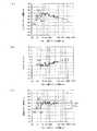
これにより、エッチング近接効果を反映した補正モデル、すなわち、エッチング近接効果補正モデルを作成する(ステップS18)。このエッチング近接効果補正モデルと、実際のエッチング近接効果により生じたエッチシフトを測定したときの実測値との間の関係を、図4(a)(b)に示す。 Thus, a correction model reflecting the etching proximity effect, that is, an etching proximity effect correction model is created (step S18). FIGS. 4A and 4B show the relationship between this etching proximity effect correction model and the actual measurement value when the etch shift caused by the actual etching proximity effect is measured.
図4(a)は、図1に示す手順で作成したエッチング近接効果補正モデルにおける、パターン間スペース302の値に対してのエッチシフトの値(グラフ中の四角のポイント)と、パターン間スペース302の値に対してのエッチシフトの実測値(グラフ中の丸のポイント)とを示している。また、横軸はパターン間スペース302の幅(nm)を示し、縦軸はエッチシフト(nm)を示している。 FIG. 4A shows an etch shift value (square point in the graph) with respect to the value of the
図4(b)は、図4(a)に示したようなエッチング近接効果補正モデルにおけるエッチシフトの値を、エッチシフトの実測値にフィッティングした結果を示している。横軸はパターン間スペース302の幅(nm)を示し、縦軸は、フィッティングしたときの残差(モデルフィッティング残差)(nm)を示している。 FIG. 4B shows the result of fitting the etch shift value in the etching proximity effect correction model as shown in FIG. 4A to the measured value of the etch shift. The horizontal axis indicates the width (nm) of the
上述したように、図12に示す手順で作成した従来のエッチング近接効果補正モデルでは、図12(b)に示したように各スペース領域において5nmを超えるモデルフィッティング残差が残っていたが、図1に示す手順で作成したエッチング近接効果補正モデルでは、図4(b)に示すように、いずれの領域においても5nmを超えるモデルフィッティング残差は発生していない。 As described above, in the conventional etching proximity effect correction model created by the procedure shown in FIG. 12, a model fitting residual exceeding 5 nm remains in each space region as shown in FIG. In the etching proximity effect correction model created by the procedure shown in No. 1, no model fitting residual exceeding 5 nm occurs in any region as shown in FIG. 4B.
よって、図1に示す手順で作成したエッチング近接効果補正モデルは、実測値との間に良い一致が得られる。したがって、高精度のエッチング近接効果補正モデルを作成することが可能となる。 Therefore, the etching proximity effect correction model created by the procedure shown in FIG. 1 is in good agreement with the actual measurement value. Therefore, it is possible to create a highly accurate etching proximity effect correction model.
なお、関数R−nは、レジスト下部形状による依存性を含めた、フォトレジストの下層に設けられる有機反射防止膜204をエッチングする際のパターン依存性を良く再現し、また、対数関数Log(R)は、ゲート配線パターン207を形成するために多結晶シリコン膜203をエッチングする際のパターン依存性を良く再現する。これにより、エッチング近接効果補正モデルには、関数R−nおよび対数関数Log(R)が線形結合された式が含まれているので、高精度を実現することが可能となっている。Note that the function R−n well reproduces the pattern dependency when etching the
つまり、従来のエッチング近接効果補正モデルの精度が低かった理由は、パターン間スペースの幅が広いスペース領域では、エッチング中の副生成物の生成およびパターン側壁への入射によって生じる側壁保護効果がパターン間スペースRのLog関数に依存すること、一方、パターン間スペースの幅が狭いスペース領域では、エッチシフトがマスクパターンのすそ引きによるパターン間スペースRの関数R−2に依存していることにより、精度が低下するという原因に対応していなかったためと考えられる。In other words, the accuracy of the conventional etching proximity effect correction model was low because the side wall protection effect caused by the formation of by-products during etching and incidence on the pattern side wall is large in the space region where the space between patterns is wide. Depending on the Log function of the space R, on the other hand, in the space region where the width of the inter-pattern space is narrow, the etch shift depends on the function R-2 of the inter-pattern space R due to the mask pattern skirting. This is probably because the cause of the decline was not addressed.
また、特に、関数R−1は、有機反射防止膜204をエッチングする際のパターン依存性を、関数R−2は、エッチングによりパターンがシフトする際の、レジストパターン205のレジスト下部形状による依存性を、非常に良く再現する。実際に、エッチング近接効果補正モデルの作成時に、関数R−nにおいて、n=3,2,1,−1をそれぞれ代入してフィッティングを行った結果、n=2,1の場合が、エッチング近接効果補正モデルの精度を高める影響度の大きいパラメータであることを確認した。それゆえ、上記関数R−nは、1≦n≦2の範囲で設定されることが望ましい。Further, in particular, the function R-1 is the pattern dependency when the
また、エッチング近接効果補正モデルが、図3に示したような一定のパターンピッチ303を有する繰り返しパターンが定められたエッチング近接効果評価パターンを用いて、算出したエッチシフトに基づいて作成されている場合、エッチシフトは容易に算出でき、パターンサイズおよびパターン間スペースサイズのパラメータも抽出するのには複雑なものとなっていないので、エッチシフトに対しての、パターンサイズおよびパターン間スペースサイズをパラメータとして用いることによるモデル化を容易に行うことが可能となる。 When the etching proximity effect correction model is created based on the calculated etch shift using the etching proximity effect evaluation pattern in which a repetitive pattern having a
ここで、エッチング近接効果補正モデルがパラメータとする、パターンサイズおよびパターン間スペースサイズについて詳細に説明する。 Here, the pattern size and the inter-pattern space size, which are parameters of the etching proximity effect correction model, will be described in detail.
図3に示したような繰り返しパターンが設定されている場合、図5(a)に示すように、パターン補正を行う点Pに対して、設定した範囲Q内に存在するパターン301の一部分311が、パターンサイズの値を抽出する対象として想定される。同様に、図5(b)に示すように、パターン補正を行う点Pに対して、設定した範囲Q内に存在するパターン間スペース302の一部分312が、パターン間スペースサイズの値を抽出する対象として想定される。 When the repetitive pattern as shown in FIG. 3 is set, as shown in FIG. 5A, a
図5(a)(b)に示した繰り返しパターンのような、1次元(図中、横方向)のパターンについては、パターンサイズは一部分311の横幅と同等の量になり、パターン間スペースサイズは一部分312の横幅と同等の量になる。ゆえに、パターン補正を行う点Pと移動していくことによって、その都度、パターンサイズおよびパターン間スペースサイズの値を抽出していくことができる。 For a one-dimensional (horizontal direction in the figure) pattern such as the repetitive pattern shown in FIGS. 5A and 5B, the pattern size is equivalent to the horizontal width of the
また、1次元のパターンではなく、例えば、2次元のパターン(縦横方向)の場合については、パターン補正を行う点Pに対して、設定した範囲Q内で直線上に見える領域がそれぞれの値を抽出する対象として想定される。つまりは、パターンサイズは、図6(a)に示すように、パターン321の領域(面積)と同等の量になり、パターン間スペースサイズは、図6(b)に示すように、設定した範囲Q内に存在するパターン間スペース322の一部分323の領域と同等の量になる。 In addition, in the case of a two-dimensional pattern (vertical and horizontal directions) instead of a one-dimensional pattern, for each point P where pattern correction is performed, an area that appears on a straight line within the set range Q has a respective value. As an object to be extracted. That is, the pattern size is equivalent to the area (area) of the
(半導体装置の製造方法)
次に、図7を参照しながら、図1に示す手順で作成したエッチング近接効果補正モデルを用いてマスクパターンの補正を行うエッチング近接効果補正工程、を含む半導体装置の製造方法について説明する。(Method for manufacturing semiconductor device)
Next, a method for manufacturing a semiconductor device including an etching proximity effect correction step of correcting a mask pattern using the etching proximity effect correction model created by the procedure shown in FIG. 1 will be described with reference to FIG.
なお、この説明では、上述した比較例としてのエッチング近接効果補正モデルを用いてマスクパターン(特にゲートの配線パターン)を補正し、その補正したマスクパターンを有するマスクを用いて微細加工プロセスにより配線パターンを基板上に形成する場合について説明するが、後述するように、比較例としてのエッチング近接効果補正モデルに替えて、本実施の形態のエッチング近接効果補正モデルを適用することもできる。 In this description, the mask pattern (particularly the gate wiring pattern) is corrected using the etching proximity effect correction model as the comparative example described above, and the wiring pattern is formed by a microfabrication process using the mask having the corrected mask pattern. However, as will be described later, the etching proximity effect correction model of the present embodiment can be applied instead of the etching proximity effect correction model as a comparative example.
図7は、半導体装置の製造方法の製造方法を示すフローチャートである。 FIG. 7 is a flowchart showing a manufacturing method of the semiconductor device manufacturing method.
まず、半導体装置を製造するための設計データ、つまりは配線パターン(ゲートを含む)を形成するためのマスクデータを作成する(ステップS21)。または、予め作成されたマスクデータを用意するという手順をとってもよい。 First, design data for manufacturing a semiconductor device, that is, mask data for forming a wiring pattern (including a gate) is created (step S21). Or you may take the procedure of preparing the mask data produced beforehand.
続いて、上記マスクデータすなわちマスクパターンに対して、図1に示す手順で作成したエッチング近接効果補正モデルを用いて、パターンサイズおよびパターン間スペースサイズの補正を行うことにより、エッチング近接効果補正を施す(ステップS22)。つまりは、エッチング近接効果補正モデルを用いたマスクパターン(特にゲートの配線パターン)の補正を行い、エッチング近接効果補正を行ったマスクデータを作成する。なお、このときのマスクパターンの補正は、図6に示したような2次元のパターンサイズおよびパターン間スペースサイズで定義したエッチング近接効果補正モデルを用いて、2次元の設計パターンに対し補正処理を行う。これにより、高精度の補正処理を実現することができる。 Subsequently, the etching proximity effect correction is performed on the mask data, that is, the mask pattern, by correcting the pattern size and the inter-pattern space size using the etching proximity effect correction model created by the procedure shown in FIG. (Step S22). That is, the mask pattern (particularly the gate wiring pattern) is corrected using the etching proximity effect correction model, and mask data subjected to the etching proximity effect correction is created. In this case, the mask pattern is corrected by correcting the two-dimensional design pattern using the etching proximity effect correction model defined by the two-dimensional pattern size and the inter-pattern space size as shown in FIG. Do. Thereby, highly accurate correction processing can be realized.
続いて、リソグラフィー近接効果補正モデルを用いて、エッチング近接効果補正を行ったマスクデータに対して、マスクパターンのパターンサイズおよびパターン間スペースサイズの補正を行うことにより、リソグラフィー近接効果補正を施す(ステップS23)。これにより、リソグラフィー近接効果補正を行ったマスクデータを作成する。なお、リソグラフィー近接効果補正モデルを用いたリソグラフィー近接効果補正の方法は、従来ある一般的な方法を好適に用いればよい。 Subsequently, using the lithography proximity effect correction model, the lithography proximity effect correction is performed by correcting the pattern size of the mask pattern and the inter-pattern space size with respect to the mask data subjected to the etching proximity effect correction (Step S1). S23). Thereby, mask data subjected to the lithography proximity effect correction is created. In addition, the conventional general method should just be used suitably for the method of the lithography proximity effect correction | amendment using a lithography proximity effect correction model.
続いて、マスクプロセス近接効果補正モデルを用いて、リソグラフィー近接効果補正を行ったマスクデータに対して、マスクパターンのパターンサイズおよびパターン間スペースサイズの補正を行うことにより、マスクプロセス近接効果補正を施す(ステップS24)。これにより、マスクプロセス近接効果補正を行ったマスクデータを作成する(ステップS25)。なお、マスクプロセス近接効果補正モデルを用いたマスクプロセス近接効果補正の方法は、従来ある一般的な方法を好適に用いればよい。 Subsequently, using the mask process proximity effect correction model, the mask process proximity effect correction is performed by correcting the mask pattern pattern size and the inter-pattern space size on the mask data subjected to the lithography proximity effect correction. (Step S24). Thereby, mask data subjected to mask process proximity effect correction is created (step S25). Note that a conventional general method may be suitably used as the mask process proximity effect correction method using the mask process proximity effect correction model.
続いて、エッチング近接効果補正、リソグラフィー近接効果補正、およびマスクプロセス近接効果補正を順に施して作成したマスクデータに基づいて、通常のフォトマスク作製方法を用いて、プロセス近接効果補正マスク(フォトマスク)を作製する(ステップS26)。その後、通常の欠陥検査装置を用いて、プロセス近接効果補正マスクのパターン欠陥の検査を行う(ステップS27)。 Subsequently, a process proximity effect correction mask (photomask) is prepared using a normal photomask manufacturing method based on mask data created by sequentially performing etching proximity effect correction, lithography proximity effect correction, and mask process proximity effect correction. Is prepared (step S26). Thereafter, a pattern defect of the process proximity effect correction mask is inspected using a normal defect inspection apparatus (step S27).
上記検査を経て不良点が発見されなかったプロセス近接効果補正マスクは、高精度なエッチング近接効果補正モデルを用いてエッチング近接効果補正が施されたマスクデータに基づいたマスクパターンを有するプロセス近接効果補正マスクとして実現される。 The process proximity effect correction mask in which no defective point was found through the above inspection has a process proximity effect correction having a mask pattern based on the mask data subjected to the etching proximity effect correction using a highly accurate etching proximity effect correction model. Realized as a mask.
続いて、リソグラフィー工程を実施する(ステップS28)。詳細には、配線パターンを形成する半導体装置の下地構造上に、プロセス近接効果補正マスクと、エッチング近接効果補正モデルの作成に用いたリソグラフィー条件とを用いて、レジストパターンを形成する。 Subsequently, a lithography process is performed (step S28). Specifically, a resist pattern is formed on a base structure of a semiconductor device on which a wiring pattern is to be formed, using a process proximity effect correction mask and the lithography conditions used to create an etching proximity effect correction model.
続いて、形成したレジストパターンに基づいて、エッチング工程を実施する(ステップS29)。詳細には、レジストパターンをマスクとして、エッチング近接効果補正モデルの作成に用いたエッチング条件で、エッチング処理を行う。これにより、下地構造に配線パターンを形成することができる(ステップS30)。 Subsequently, an etching process is performed based on the formed resist pattern (step S29). Specifically, the etching process is performed under the etching conditions used to create the etching proximity effect correction model using the resist pattern as a mask. As a result, a wiring pattern can be formed on the underlying structure (step S30).
これにより形成された配線パターン、特にゲートの配線パターンは、エッチング近接効果補正、リソグラフィー近接効果補正、およびマスクプロセス近接効果補正を順に施して作成したマスクデータに基づいて形成されたものであるので、設計寸法通りに精度良く形成することが可能となる。また、これにより、ゲート線幅のばらつきを抑制しゲートの微細化を行うことができるので、トランジスタの高速化や高集積化を実現することが可能となる。 Since the wiring pattern formed by this, particularly the wiring pattern of the gate, is formed based on mask data created by performing etching proximity effect correction, lithography proximity effect correction, and mask process proximity effect correction in order, It becomes possible to form accurately according to the design dimensions. In addition, this makes it possible to reduce the gate line width and reduce the gate size, so that high speed and high integration of the transistor can be realized.
ところで、上述した半導体装置の製造方法の説明では、それぞれ独立に作成した、エッチング近接効果補正モデル、リソグラフィー近接効果補正モデル、およびマスクプロセス近接効果補正モデルを用いる場合について示した。この場合、1つの近接効果補正モデルに誤差があれば、他の近接効果補正ではその誤差は補正されないため、最終的に形成される配線パターンの線幅の誤差が大きくなる。この一例について説明する。 By the way, in the description of the semiconductor device manufacturing method described above, a case where an etching proximity effect correction model, a lithography proximity effect correction model, and a mask process proximity effect correction model, which are created independently, is shown. In this case, if there is an error in one proximity effect correction model, the error is not corrected in other proximity effect corrections, so that the line width error of the finally formed wiring pattern becomes large. An example of this will be described.
図8は、リソグラフィー近接効果補正モデルに誤差があり、図1に示す手順で作成したエッチング近接効果補正モデルを用いてエッチング近接効果補正を行う場合における、(a)はレジストパターン線幅のパターン依存性を示すグラフであり、(b)はエッチシフトのパターン依存性を示すグラフであり、(c)は配線パターン線幅のパターン依存性を示すグラフである。図8(a)〜(c)では、横軸はパターン間スペースの幅(nm)を示し、縦軸はレジストパターン線幅(nm)、エッチシフト(nm)、配線パターン線幅(nm)をそれぞれ示している。 FIG. 8 shows an error in the lithography proximity effect correction model, and FIG. 8A shows the pattern dependence of the resist pattern line width when the etching proximity effect correction is performed using the etching proximity effect correction model created by the procedure shown in FIG. (B) is a graph showing the pattern dependence of the etch shift, and (c) is a graph showing the pattern dependence of the wiring pattern line width. 8A to 8C, the horizontal axis indicates the width (nm) of the inter-pattern space, and the vertical axis indicates the resist pattern line width (nm), the etch shift (nm), and the wiring pattern line width (nm). Each is shown.
図8(a)に示すように、エッチング近接効果補正を行う場合、エッチング近接効果・リソグラフィー近接効果補正後の理想的なレジストパターン線幅のパターン間スペース依存性501は、図8(b)に示す、エッチング後の実際のエッチシフトのパターン間スペース依存性504を補正したものである。 As shown in FIG. 8A, when etching proximity effect correction is performed, the
しかし、実際には、一例として、リソグラフィー近接効果補正モデルの作成過程で生じるリソグラフィー近接効果補正モデルの誤差502が生じる場合が多い。そのため、エッチング近接効果・リソグラフィー近接効果補正後の実際のレジストパターン線幅のパターン間スペース依存性503は、パターン間スペースが400nm以下の領域でレジストパターン線幅が細くなる方向に、最大で約9nmの誤差が発生する。 However, in practice, as an example, an
なお、図8(c)に示すように、エッチング近接効果補正を行う場合、エッチング近接効果・リソグラフィー近接効果補正後の理想的な配線パターン線幅のパターン間スペース依存性505は、パターン間スペースの値によらず一定である。 As shown in FIG. 8C, when the etching proximity effect correction is performed, the
しかし、エッチング後の実際の配線パターン線幅のパターン間スペース依存性506は、実際のエッチシフトのパターン間スペース依存性504の影響は補正されているが、パターン間スペースが400nm以下の領域でレジストパターン線幅が細くなる方向に最大で発生した約9nmのリソグラフィー近接効果補正モデルの誤差502の影響を受け、結果として配線パターン線幅のパターン間ばらつき507が残ってしまう(ばらつき幅:約12.5nm)。 However, the
したがって、リソグラフィー近接効果補正モデルに誤差がある場合、図1に示す手順で作成したエッチング近接効果補正モデルを用いてエッチング近接効果補正を行うことで、実際の配線パターンの線幅のパターン間ばらつきを低減することが可能となってはいるが、さらなる低減が望まれている。 Therefore, if there is an error in the lithography proximity effect correction model, the etching proximity effect correction is performed using the etching proximity effect correction model created in the procedure shown in FIG. Although it is possible to reduce, further reduction is desired.
本発明では、このような配線パターン線幅のパターン間ばらつきをさらに低減するために、例えばリソグラフィー近接効果補正モデルの誤差をエッチング近接効果補正で吸収することで、最終のパターン補正精度をさらに向上することが可能となっている。次に、本発明のエッチング近接効果補正モデルの作成方法の一実施例について説明する。 In the present invention, in order to further reduce the variation in the wiring pattern line width between patterns, for example, the error of the lithography proximity effect correction model is absorbed by the etching proximity effect correction, thereby further improving the final pattern correction accuracy. It is possible. Next, an embodiment of a method for creating an etching proximity effect correction model of the present invention will be described.
(エッチング近接効果補正モデルの作成方法)
本発明の一実施形態について図9,10に基づいて説明すれば、以下の通りである。(How to create an etching proximity effect correction model)
An embodiment of the present invention will be described below with reference to FIGS.
図9は、本実施の形態のエッチング近接効果補正モデルの作成方法を示すフローチャートである。 FIG. 9 is a flowchart showing a method for creating an etching proximity effect correction model according to the present embodiment.
まず、図1を用いて説明した作成方法のステップS11〜S12と同様に、下地構造を形成し(ステップS31)、その上にレジストパターンを形成する(ステップS32)。 First, similarly to steps S11 to S12 of the creation method described with reference to FIG. 1, a base structure is formed (step S31), and a resist pattern is formed thereon (step S32).
続いて、リソグラフィー近接効果補正モデルを用いて、形成したレジストパターンに対しシミュレーションを行うことにより、レジストパターン線幅を算出する(ステップS33)。これにより、レジストパターン線幅のシミュレーション値を得る。 Subsequently, the resist pattern line width is calculated by performing simulation on the formed resist pattern using the lithography proximity effect correction model (step S33). Thereby, a simulation value of the resist pattern line width is obtained.
このとき、リソグラフィー近接効果補正モデルとしては、図7に示したステップS23のリソグラフィー近接効果補正工程において使用するリソグラフィー近接効果補正モデルを用い、リソグラフィー近接効果補正モデル作成ツールのシミュレーション機能を用いて、エッチング近接効果評価パターンの設計レイアウトから、レジストパターン形状をシミュレーションし、その線幅を測定する。 At this time, as the lithography proximity effect correction model, the lithography proximity effect correction model used in the lithography proximity effect correction process of step S23 shown in FIG. 7 is used, and the simulation function of the lithography proximity effect correction model creation tool is used for etching. The resist pattern shape is simulated from the design layout of the proximity effect evaluation pattern, and the line width is measured.
この際、レジストパターン線幅の実測値とシミュレーション値との間には、以下の式(2)の関係が成り立っている。 At this time, the relationship of the following formula (2) is established between the actually measured value and the simulation value of the resist pattern line width.
レジストパターン線幅(実測値)=レジストパターン線幅(シミュレーション値)+リソグラフィー近接効果補正モデルの誤差 …式(2)
続いて、図1を用いて説明した作成方法のステップS14〜S15と同様に、ゲート配線パターンを形成し(ステップS34)、ゲート配線パターン線幅を測定する(ステップS35)。これにより、ゲート配線パターン線幅の実測値を得る。Resist pattern line width (actual value) = resist pattern line width (simulation value) + lithography proximity effect correction model error (2)
Subsequently, a gate wiring pattern is formed (step S34) and the gate wiring pattern line width is measured (step S35) in the same manner as steps S14 to S15 of the production method described with reference to FIG. Thereby, an actual measurement value of the gate wiring pattern line width is obtained.
続いて、ステップS34で行ったエッチング工程でのパターンシフトである、エッチシフトを算出する(ステップS36)。すなわち、エッチングによるパターンのシフト量を算出する。この際、リソグラフィー近接効果補正モデルを用いて算出したレジストパターン線幅のシミュレーション値と、ゲート配線パターン線幅の実測値とから、以下の式(3)を用いてエッチシフトを算出する。 Subsequently, an etch shift, which is a pattern shift in the etching process performed in step S34, is calculated (step S36). That is, the shift amount of the pattern due to etching is calculated. At this time, the etch shift is calculated by using the following equation (3) from the simulation value of the resist pattern line width calculated using the lithography proximity effect correction model and the measured value of the gate wiring pattern line width.
エッチシフト=ゲート配線パターン線幅(実測値)−レジストパターン線幅(シミュレーション値) …式(3)。 Etch shift = gate wiring pattern line width (actual value) −resist pattern line width (simulation value) Equation (3).
ここで、式(2)および式(3)から、以下の式(4)の関係が成り立つため、上記手法を用いることで、実測値から算出されたエッチシフトに加えて、リソグラフィー近接効果補正モデルの誤差を含んだエッチシフトを算出することができる。 Here, since the relationship of the following formula (4) is established from the formula (2) and the formula (3), the lithography proximity effect correction model is added to the etch shift calculated from the actual measurement value by using the above method. The etch shift including the error can be calculated.
エッチシフト=配線パターン線幅(実測値)−レジストパターン線幅(実測値)+リソグラフィー近接効果補正モデルの誤差 …式(4)
続いて、図1を用いて説明した作成方法のステップS17と同様に、ステップS36にて算出したエッチシフトに対して、パターンサイズおよびパターン間スペースサイズをパラメータとする補正モデルを用いて、最小二乗法によるフィッティングを行う(ステップS37)。これにより、エッチング近接効果補正モデルを作成し得る(ステップS38)。Etch shift = wiring pattern line width (actual value) −resist pattern line width (actual value) + lithographic proximity effect correction model error (Equation 4)
Subsequently, similarly to step S17 of the creation method described with reference to FIG. 1, the correction model having the pattern size and the inter-pattern space size as parameters is used for the etch shift calculated in step S36. Fitting by multiplication is performed (step S37). Thereby, an etching proximity effect correction model can be created (step S38).
図1に示した比較例としてのエッチング近接効果補正モデルの作成方法では、ステップS16でエッチシフトを算出する際、ステップS13で測定したレジストパターン線幅の実測値と、ステップS15で測定した配線パターン線幅(ゲート配線パターン線幅)の実測値とを用いて計算している。 In the method of creating an etching proximity effect correction model as a comparative example shown in FIG. 1, when calculating the etch shift in step S16, the measured value of the resist pattern line width measured in step S13 and the wiring pattern measured in step S15. Calculation is performed using the actual measurement value of the line width (gate wiring pattern line width).
これに対し、図9に示した本実施の形態のエッチング近接効果補正モデルの作成方法では、ステップS36でエッチシフトを算出する際、ステップS33でリソグラフィー近接効果補正モデルを用いてシミュレーションを行うことにより算出したレジストパターン線幅のシミュレーション値と、ステップS35で測定した配線パターン線幅の実測値とを用いて計算している。 On the other hand, in the method for creating the etching proximity effect correction model of the present embodiment shown in FIG. 9, when calculating the etch shift in step S36, simulation is performed using the lithography proximity effect correction model in step S33. Calculation is performed using the calculated simulation value of the resist pattern line width and the actually measured value of the wiring pattern line width measured in step S35.
すなわち、エッチシフトは、リソグラフィー近接効果補正モデルを用いてシミュレーションを行うことにより算出したレジストパターンの線幅のシミュレーション値を用いて算出している。それゆえ、リソグラフィー近接効果補正モデルに誤差がある場合、この誤差をエッチシフトの中に含めることが可能となり、誤差を考慮したフィッティングを行うことが可能となる。 That is, the etch shift is calculated using a simulation value of the line width of the resist pattern calculated by performing a simulation using the lithography proximity effect correction model. Therefore, if there is an error in the lithography proximity effect correction model, this error can be included in the etch shift, and fitting in consideration of the error can be performed.
よって、リソグラフィー近接効果補正モデルの誤差を吸収したエッチング近接効果補正モデルを作成することが可能となり、パターン補正精度をさらに向上することが可能となる。また、エッチング近接効果補正モデルは、パターンサイズおよびパターン間スペースサイズで定義されるので、精度良く作成される。したがって、非常に高精度のエッチング近接効果補正モデルを作成することが可能となる。 Therefore, it is possible to create an etching proximity effect correction model that absorbs errors in the lithography proximity effect correction model, and it is possible to further improve the pattern correction accuracy. Further, the etching proximity effect correction model is defined by the pattern size and the inter-pattern space size, and thus is created with high accuracy. Therefore, it is possible to create a highly accurate etching proximity effect correction model.
また、本実施の形態のエッチング近接効果補正モデルの作成方法では、レジストパターン線幅の測定工程を削減することができるため、図1に示した比較例としてのエッチング近接効果補正モデルの作成方法と比較して、モデル作成期間の短縮が可能となる。 Further, in the etching proximity effect correction model creation method of the present embodiment, the resist pattern line width measurement process can be reduced, so that the etching proximity effect correction model creation method as a comparative example shown in FIG. In comparison, the model creation period can be shortened.
図10は、リソグラフィー近接効果補正モデルに誤差があり、図9に示す手順で作成したエッチング近接効果補正モデルを用いてエッチング近接効果補正を行う場合における、(a)はレジストパターン線幅のパターン依存性を示すグラフであり、(b)はエッチシフトのパターン依存性を示すグラフであり、(c)は配線パターン線幅のパターン依存性を示すグラフである。図10(a)〜(c)では、横軸はパターン間スペースの幅(nm)を示し、縦軸はレジストパターン線幅(nm)、エッチシフト(nm)、配線パターン線幅(nm)をそれぞれ示している。 10 shows an error in the lithography proximity effect correction model, and FIG. 10A shows the pattern dependence of the resist pattern line width when the etching proximity effect correction is performed using the etching proximity effect correction model created by the procedure shown in FIG. (B) is a graph showing the pattern dependence of the etch shift, and (c) is a graph showing the pattern dependence of the wiring pattern line width. 10A to 10C, the horizontal axis indicates the width (nm) of the space between patterns, and the vertical axis indicates the resist pattern line width (nm), the etch shift (nm), and the wiring pattern line width (nm). Each is shown.
図10(a)に示すように、エッチング近接効果補正を行う場合、エッチング近接効果・リソグラフィー近接効果補正後の理想的なレジストパターン線幅のパターン間スペース依存性601は、図10(b)に示す、エッチング後の実際のエッチシフトのパターン間スペース依存性604を補正したものである。 As shown in FIG. 10A, when etching proximity effect correction is performed, the
ここで、実際には、リソグラフィー近接効果補正モデルの作成過程で生じるリソグラフィー近接効果補正モデルの誤差602が生じる場合が多く、一例として、パターン間スペースが400nm以下の領域でレジストパターン線幅が細くなる方向に、最大で約9nmの誤差が発生する。 Here, in practice, there are many cases where an
ところが、本実施例では、エッチング近接効果補正を行う際に用いるエッチング近接効果補正モデルが、リソグラフィー近接効果補正モデルの誤差602を吸収している。よって、誤差602がある場合でも、エッチング近接効果・リソグラフィー近接効果補正後の実際のレジストパターン線幅のパターン間スペース依存性603は、誤差602を吸収して、理想的なレジストパターン線幅のパターン間スペース依存性601に非常に近づけることが可能となっている。 However, in this embodiment, the etching proximity effect correction model used when performing the etching proximity effect correction absorbs the
また、図10(c)に示すように、エッチング近接効果補正を行う場合、エッチング近接効果・リソグラフィー近接効果補正後の理想的な配線パターン線幅のパターン間スペース依存性605は、パターン間スペースの値によらず一定である。 Further, as shown in FIG. 10C, when the etching proximity effect correction is performed, the
本実施例では、エッチング後の実際の配線パターン線幅のパターン間スペース依存性606は、実際のエッチシフトのパターン間スペース依存性604、および、パターン間スペースが400nm以下の領域でレジストパターン線幅が細くなる方向に最大で発生した約9nmのリソグラフィー近接効果補正モデルの誤差602の影響が補正されているので、パターン間ばらつき607を非常に小さくすることが可能となっている(ばらつき幅:約7.9nm)。 In this embodiment, the
このように、本実施の形態のエッチング近接効果補正モデルを用いたマスクパターンの補正では、設計パターン(設計データ)に対し、エッチング近接効果補正処理を行う際に、リソグラフィー近接効果補正モデルの誤差を吸収することができる。よって、エッチング近接効果に対するマスクパターンの補正を非常に高精度で行うことが可能となり、設計寸法に非常に近づく配線パターンの形成につなげることが可能となる。 As described above, in the mask pattern correction using the etching proximity effect correction model of the present embodiment, when the etching proximity effect correction process is performed on the design pattern (design data), the error of the lithography proximity effect correction model is reduced. Can be absorbed. Therefore, it is possible to correct the mask pattern with respect to the etching proximity effect with very high accuracy, and to lead to formation of a wiring pattern that is very close to the design dimension.
つまりは、図7を参照して説明した半導体装置の製造において、ステップS22のエッチング近接効果補正工程で、マスクパターンに対し、本実施の形態のエッチング近接効果補正モデルを用いてエッチング近接効果に対する補正を行うことによって、リソグラフィー近接効果補正モデルに誤差がある場合であっても、マスクパターンの補正を非常に高精度で行うことが可能となり、最終の配線パターンに対してさらに高精度な補正が可能となる。 That is, in the manufacture of the semiconductor device described with reference to FIG. 7, in the etching proximity effect correction step in step S22, correction for the etching proximity effect is performed on the mask pattern using the etching proximity effect correction model of the present embodiment. By doing this, even if there is an error in the lithography proximity effect correction model, it is possible to correct the mask pattern with very high accuracy, and it is possible to correct the final wiring pattern with higher accuracy. It becomes.
またこれにより、エッチング近接効果に対する補正が非常に高精度で行われたマスクパターンを有するプロセス近接効果補正マスクを作成することが可能となる。 This also makes it possible to create a process proximity effect correction mask having a mask pattern in which correction for the etching proximity effect is performed with very high accuracy.
さらには、上記プロセス近接効果補正マスクを用いて配線パターンが形成されるので、リソグラフィー近接効果補正モデルに誤差がある場合であっても、設計寸法通りの非常に優れた精度で、配線パターンを形成することが可能となる。すなわち、所望の寸法を持つ配線パターンが非常に高精度で形成された半導体装置を実現することが可能となる。 Furthermore, since the wiring pattern is formed using the above-mentioned process proximity effect correction mask, even if there is an error in the lithography proximity effect correction model, the wiring pattern is formed with very good accuracy according to the design dimensions. It becomes possible to do. That is, it is possible to realize a semiconductor device in which a wiring pattern having a desired dimension is formed with very high accuracy.
なお、上述した説明では、エッチング近接効果に対するマスクパターンの補正を、パターンサイズおよびパターン間スペースサイズをパラメータとするエッチング近接効果補正モデルを用いて行う場合について説明したが、エッチング近接効果補正モデルから、様々なパターンサイズおよびパターン間スペースサイズに対して、エッチシフトを計算することが可能になるため、パターンサイズとパターン間スペースサイズとの組み合わせにより補正量を規定した補正ルールを用いて、エッチング近接効果に対するマスクパターンの補正を行うこともできる。次に、この補正ルールの一例について説明する。 In the above description, the mask pattern correction for the etching proximity effect is described using the etching proximity effect correction model using the pattern size and the inter-pattern space size as parameters. Etch shift can be calculated for various pattern sizes and inter-pattern space sizes, so the etching proximity effect can be achieved using a correction rule that defines the correction amount by combining the pattern size and inter-pattern space size. It is also possible to correct the mask pattern for. Next, an example of this correction rule will be described.
(補正ルール)
図9に示す手順で作成したエッチング近接効果補正モデルを用いることにより、パターンの幅およびパターン間スペースの幅に対して、補正量を一定の間隔(例えば1nm)で算出する。そして、算出した補正量と、パターンの幅およびパターン間スペースの幅との組合せ(補正ルール表)を作成する。これにより、補正ルールを規定することができる。(Correction rule)
By using the etching proximity effect correction model created by the procedure shown in FIG. 9, the correction amount is calculated at a constant interval (for example, 1 nm) with respect to the width of the pattern and the width of the space between patterns. Then, a combination (correction rule table) of the calculated correction amount, the width of the pattern, and the width of the space between patterns is created. Thereby, a correction rule can be defined.
補正ルールを用いた補正処理は、図5に示したような横方向スペースによる1次元(横方向)のみの補正を想定している。つまりは、補正処理を行うパターンのレイアウトにおいて、パターンのエッジを一定の長さ(例えば50nm)に細分化してエッジセグメントを形成する。そして、それぞれのエッジセグメントに対して、パターンの幅およびパターン間スペースの幅を測定する。そして、補正ルール表を参照しながら、測定したパターンの幅およびパターン間スペースの幅から、補正量を抽出する。この補正量の分だけ、エッジセグメント内のパターンのエッジを移動させることにより、パターン補正処理を行う。 The correction process using the correction rule assumes a one-dimensional (horizontal direction) correction using a horizontal space as shown in FIG. That is, in the layout of the pattern to be corrected, the edge of the pattern is subdivided into a certain length (for example, 50 nm) to form edge segments. Then, the width of the pattern and the width of the inter-pattern space are measured for each edge segment. Then, referring to the correction rule table, the correction amount is extracted from the width of the measured pattern and the width of the inter-pattern space. Pattern correction processing is performed by moving the edge of the pattern in the edge segment by this correction amount.
エッチング近接効果補正モデルを直接用いた補正処理は、図6に示したような2次元の設計パターンに対し補正処理を行うが、エッチング近接効果補正モデルを用いて算出したデータにより規定した補正ルールを用いた補正処理は、図5に示したような横方向のスペースによる1次元(横方向)のみの補正処理を行う。 In the correction process using the etching proximity effect correction model directly, the correction process is performed on the two-dimensional design pattern as shown in FIG. 6, but the correction rule defined by the data calculated using the etching proximity effect correction model is used. The correction process used is a one-dimensional (horizontal direction) correction process using a horizontal space as shown in FIG.
それゆえ、補正ルールを用いた補正処理は、補正処理の際に、各エッジセグメントに対し、1次元(横方向)のみのパターンサイズおよびパターン間スペースサイズを検出すればよいため、補正処理にかかる時間を短縮することが可能となる。但し、1次元(横方向)のみのパターンサイズおよびパターン間スペースサイズしか考慮しないため、補正精度は幾分低下する。 Therefore, the correction process using the correction rule requires the correction process because it is only necessary to detect the one-dimensional (lateral direction) pattern size and inter-pattern space size for each edge segment during the correction process. Time can be shortened. However, since only one-dimensional (horizontal direction) pattern size and inter-pattern space size are considered, the correction accuracy is somewhat lowered.
なお、本発明は上述した実施形態に限定されるものではなく、請求項に示した範囲で種々の変更が可能である。すなわち、請求項に示した範囲で適宜変更した技術的手段を組み合わせて得られる実施形態についても本発明の技術的範囲に含まれる。 In addition, this invention is not limited to embodiment mentioned above, A various change is possible in the range shown to the claim. That is, embodiments obtained by combining technical means appropriately modified within the scope of the claims are also included in the technical scope of the present invention.
本発明は、フォトマスクなどのマスクパターンを補正する方法に関する分野に好適に用いることができるだけでなく、マスクを用いて形成された配線パターンが設けられる半導体装置に関する分野、さらには、半導体装置の製造に関する分野、例えば、リソグラフィー工程やエッチング工程に関する分野にも広く用いることができる。 INDUSTRIAL APPLICABILITY The present invention can be suitably used in a field related to a method for correcting a mask pattern such as a photomask, and also relates to a field related to a semiconductor device provided with a wiring pattern formed using a mask, and further to manufacturing a semiconductor device. For example, it can be widely used in fields related to lithography processes and etching processes.
201 半導体基板
202 ゲート絶縁膜
203 多結晶シリコン膜
204 有機反射防止膜
205 レジストパターン
206 レジストパターン線幅
207 ゲート配線パターン
208 ゲート配線パターン線幅
301,321 パターン
302,322 パターン間スペース
303 パターンピッチDESCRIPTION OF
Claims (10)
Translated fromJapanese基板の配線形成面にレジストを形成し、評価用パターンを搭載した評価用フォトマスクを用いて該レジストにリソグラフィー処理を行うことにより、評価用パターンが転写されたレジストパターンを形成するステップと、
上記レジストパターンに対し、リソグラフィー近接効果補正モデルを用いてシミュレーションを行うことにより、該レジストパターンの線幅のシミュレーション値を算出するステップと、
上記レジストパターンをマスクとして上記基板の配線形成面をエッチングすることにより、配線パターンを形成するステップと、
上記配線パターンの線幅を測定するステップと、
上記レジストパターンの線幅のシミュレーション値と、上記配線パターンの線幅の実測値とから、上記エッチングによるパターンのシフト量を算出するステップと、
上記シフト量に対し、パターンサイズおよびパターン間スペースサイズをパラメータとする補正モデルを用いて、最小二乗法によるフィッティングを行うことにより、エッチング近接効果補正モデルを作成するステップと、を含み、
上記補正モデルは、上記パターン間スペースサイズのパラメータをRとする場合、関数R−n(n:正の実数)および対数関数Log(R)が線形結合された式を少なくとも含んでいることを特徴とするエッチング近接効果補正モデルの作成方法。A method of creating an etching proximity effect correction model for calculating a correction amount for performing etching proximity effect correction on a mask pattern,
Forming a resist on the wiring formation surface of the substrate, and performing a lithography process on the resist using an evaluation photomask mounted with the evaluation pattern, thereby forming a resist pattern to which the evaluation pattern is transferred;
Calculating a simulation value of the line width of the resist pattern by performing simulation using the lithography proximity effect correction model for the resist pattern;
Etching the wiring formation surface of the substrate using the resist pattern as a mask to form a wiring pattern;
Measuring the line width of the wiring pattern;
Calculating a shift amount of the pattern by the etching from a simulation value of the line width of the resist pattern and an actual measurement value of the line width of the wiring pattern;
The shift amount to, using the correction model parameters a pattern size and pattern spacing size, by performing fitting by the least squares method,see containing and creating an etching proximity effect correction model,and
The correction modelincludes at least an expression in which afunction R−n(n: positive real number) and a logarithmic function Log (R) are linearly combinedwhen the parameter of the inter-pattern space size is R. A method for creating an etching proximity effect correction model.
基板の配線形成面に形成されたレジストパターンに対しリソグラフィー近接効果補正モデルを用いてシミュレーションを行うことにより算出された、該レジストパターンの線幅のシミュレーション値と、上記レジストパターンをマスクとして上記基板の配線形成面をエッチングすることにより形成された配線パターンの線幅の実測値と、から算出された上記エッチングによるパターンのシフト量に対し、パターンサイズおよびパターン間スペースサイズをパラメータとする補正モデルを用いて、最小二乗法によるフィッティングを行うことにより作成されており、 A simulation value of the line width of the resist pattern calculated by performing a simulation using a lithography proximity effect correction model on the resist pattern formed on the wiring formation surface of the substrate, and the resist pattern as a mask. A correction model using the pattern size and the inter-pattern space size as parameters for the pattern shift amount calculated from the measured line width of the wiring pattern formed by etching the wiring formation surface and the above-described etching is used. Is created by fitting using the least squares method,
上記補正モデルは、上記パターン間スペースサイズのパラメータをRとする場合、関数R The correction model has a function R where R is a parameter of the inter-pattern space size.−n-N(n:正の実数)および対数関数Log(R)が線形結合された式を少なくとも含んでいることを特徴とするエッチング近接効果補正モデル。An etching proximity effect correction model characterized in that (n: positive real number) and logarithmic function Log (R) include at least a linearly combined expression.
上記微細加工プロセスを実施する前に、エッチング近接効果に対する上記マスクパターンの補正を、請求項4または5に記載のエッチング近接効果補正モデルを用いて行うことを特徴とするマスクパターンの補正方法。 6. The mask pattern correction method according to claim 4, wherein the correction of the mask pattern with respect to the etching proximity effect is performed using the etching proximity effect correction model according to claim 4 or 5 before performing the microfabrication process.
マスクパターンのデータに対し、少なくとも、エッチング近接効果補正モデルを用いてエッチング近接効果に対する補正、およびリソグラフィー近接効果補正モデルを用いてリソグラフィー近接効果に対する補正を含む補正を行うステップと、 Performing at least correction including correction for etching proximity effect using an etching proximity effect correction model and correction for lithography proximity effect using a lithography proximity effect correction model for mask pattern data;
上記補正を行ったマスクパターンのデータに基づいてマスクを作成するステップと、 Creating a mask based on the mask pattern data subjected to the correction, and
上記作成したマスクを用いて、微細加工プロセスにより配線パターンを形成する工程と、を含み、 Using the mask created above, forming a wiring pattern by a microfabrication process,
上記エッチング近接効果補正モデルとしては、請求項4または5に記載のエッチング近接効果補正モデルを用いることを特徴とする半導体装置の製造方法。 6. The method for manufacturing a semiconductor device according to claim 4, wherein the etching proximity effect correction model uses the etching proximity effect correction model according to claim 4.
Priority Applications (1)
| Application Number | Priority Date | Filing Date | Title |
|---|---|---|---|
| JP2009080348AJP5356089B2 (en) | 2009-03-27 | 2009-03-27 | Etching proximity effect correction model creation method, etching proximity effect correction model, mask pattern correction method, photomask, semiconductor device manufacturing method, and semiconductor device |
Applications Claiming Priority (1)
| Application Number | Priority Date | Filing Date | Title |
|---|---|---|---|
| JP2009080348AJP5356089B2 (en) | 2009-03-27 | 2009-03-27 | Etching proximity effect correction model creation method, etching proximity effect correction model, mask pattern correction method, photomask, semiconductor device manufacturing method, and semiconductor device |
Publications (2)
| Publication Number | Publication Date |
|---|---|
| JP2010232542A JP2010232542A (en) | 2010-10-14 |
| JP5356089B2true JP5356089B2 (en) | 2013-12-04 |
Family
ID=43048063
Family Applications (1)
| Application Number | Title | Priority Date | Filing Date |
|---|---|---|---|
| JP2009080348AActiveJP5356089B2 (en) | 2009-03-27 | 2009-03-27 | Etching proximity effect correction model creation method, etching proximity effect correction model, mask pattern correction method, photomask, semiconductor device manufacturing method, and semiconductor device |
Country Status (1)
| Country | Link |
|---|---|
| JP (1) | JP5356089B2 (en) |
Cited By (2)
| Publication number | Priority date | Publication date | Assignee | Title |
|---|---|---|---|---|
| US10691016B2 (en) | 2017-10-31 | 2020-06-23 | Samsung Electronincs Co., Ltd. | Methods of forming semiconductors using etching effect predictions and methods for determining input parameters for semiconductor formation |
| US12223249B2 (en) | 2020-12-29 | 2025-02-11 | Samsung Electronics Co., Ltd. | Etch-modeling system and method of manufacturing semiconductor device using the same |
Families Citing this family (4)
| Publication number | Priority date | Publication date | Assignee | Title |
|---|---|---|---|---|
| KR101855803B1 (en) | 2012-02-22 | 2018-05-10 | 삼성전자주식회사 | Method for Process Proximity Correction |
| JP5758423B2 (en) | 2013-02-26 | 2015-08-05 | 株式会社東芝 | How to create a mask layout |
| US8856695B1 (en) | 2013-03-14 | 2014-10-07 | Samsung Electronics Co., Ltd. | Method for generating post-OPC layout in consideration of top loss of etch mask layer |
| JP7256287B2 (en)* | 2019-03-25 | 2023-04-11 | エーエスエムエル ネザーランズ ビー.ブイ. | Method for determining patterns in a patterning process |
Family Cites Families (2)
| Publication number | Priority date | Publication date | Assignee | Title |
|---|---|---|---|---|
| JP2007140485A (en)* | 2005-10-18 | 2007-06-07 | Sharp Corp | Parameter extraction apparatus and parameter extraction method in simulation, mask pattern data created by this method, photomask and semiconductor device created by this mask pattern data |
| JP2007219208A (en)* | 2006-02-17 | 2007-08-30 | Sony Corp | Pattern correction device, pattern correction program, pattern correction method and method for manufacturing semiconductor device |
- 2009
- 2009-03-27JPJP2009080348Apatent/JP5356089B2/enactiveActive
Cited By (2)
| Publication number | Priority date | Publication date | Assignee | Title |
|---|---|---|---|---|
| US10691016B2 (en) | 2017-10-31 | 2020-06-23 | Samsung Electronincs Co., Ltd. | Methods of forming semiconductors using etching effect predictions and methods for determining input parameters for semiconductor formation |
| US12223249B2 (en) | 2020-12-29 | 2025-02-11 | Samsung Electronics Co., Ltd. | Etch-modeling system and method of manufacturing semiconductor device using the same |
Also Published As
| Publication number | Publication date |
|---|---|
| JP2010232542A (en) | 2010-10-14 |
Similar Documents
| Publication | Publication Date | Title |
|---|---|---|
| JP4511582B2 (en) | Mask pattern correction method, photomask, and semiconductor device manufacturing method | |
| JP4675854B2 (en) | Pattern evaluation method, evaluation apparatus, and pattern evaluation program | |
| JP5356089B2 (en) | Etching proximity effect correction model creation method, etching proximity effect correction model, mask pattern correction method, photomask, semiconductor device manufacturing method, and semiconductor device | |
| CN106158679A (en) | Method for improving semiconductor device manufacturing process by combining wafer physical measurement and digital simulation | |
| CN116520646A (en) | Method for improving overlay accuracy | |
| CN103472672A (en) | Correction method of optical proximity correction model | |
| US20080070414A1 (en) | Method for designing mask and method for manufacturing semiconductor device employing thereof | |
| TWI421908B (en) | Method for constructing opc model | |
| US8443309B2 (en) | Multifeature test pattern for optical proximity correction model verification | |
| JP2008139688A (en) | Semiconductor integrated circuit manufacturing method, mask manufacturing method, semiconductor mask data manufacturing apparatus, mask pattern correction method, and design layout correction method | |
| JP2011028120A (en) | Method for forming pattern, program for forming pattern, and method for manufacturing semiconductor device | |
| US8127257B2 (en) | Designing method of photo-mask and method of manufacturing semiconductor device using the photo-mask | |
| CN112541545B (en) | Method for predicting CDSEM image after etching process based on machine learning | |
| KR20090000868A (en) | Optical proximity effect correction method | |
| CN100369040C (en) | A Simulation Method of Variable Deviation Etching under Subwavelength Lithography Conditions | |
| CN117742067A (en) | Preparation method, device and photolithography method of phase-shift photomask | |
| US20100159617A1 (en) | Semiconductor-device manufacturing method and exposure method | |
| CN114925635B (en) | OPC model data weight setting method | |
| KR20070109117A (en) | How to make a mask | |
| US8336004B2 (en) | Dimension assurance of mask using plurality of types of pattern ambient environment | |
| US20080044739A1 (en) | Correction Of Resist Critical Dimension Variations In Lithography Processes | |
| JP5703910B2 (en) | Mask pattern data generation method, mask manufacturing method, mask, and mask pattern data generation program | |
| JP2005072213A (en) | Charged-particle beam exposure method | |
| KR20030070442A (en) | Method of a semiconductor process simulation | |
| JP2014238479A (en) | Method for creating mask data |
Legal Events
| Date | Code | Title | Description |
|---|---|---|---|
| A621 | Written request for application examination | Free format text:JAPANESE INTERMEDIATE CODE: A621 Effective date:20110223 | |
| A977 | Report on retrieval | Free format text:JAPANESE INTERMEDIATE CODE: A971007 Effective date:20111027 | |
| A131 | Notification of reasons for refusal | Free format text:JAPANESE INTERMEDIATE CODE: A131 Effective date:20130305 | |
| A521 | Request for written amendment filed | Free format text:JAPANESE INTERMEDIATE CODE: A523 Effective date:20130411 | |
| TRDD | Decision of grant or rejection written | ||
| A01 | Written decision to grant a patent or to grant a registration (utility model) | Free format text:JAPANESE INTERMEDIATE CODE: A01 Effective date:20130730 | |
| A61 | First payment of annual fees (during grant procedure) | Free format text:JAPANESE INTERMEDIATE CODE: A61 Effective date:20130828 | |
| R150 | Certificate of patent or registration of utility model | Ref document number:5356089 Country of ref document:JP Free format text:JAPANESE INTERMEDIATE CODE: R150 Free format text:JAPANESE INTERMEDIATE CODE: R150 | |
| S531 | Written request for registration of change of domicile | Free format text:JAPANESE INTERMEDIATE CODE: R313531 | |
| R350 | Written notification of registration of transfer | Free format text:JAPANESE INTERMEDIATE CODE: R350 | |
| S111 | Request for change of ownership or part of ownership | Free format text:JAPANESE INTERMEDIATE CODE: R313113 | |
| R371 | Transfer withdrawn | Free format text:JAPANESE INTERMEDIATE CODE: R371 | |
| S111 | Request for change of ownership or part of ownership | Free format text:JAPANESE INTERMEDIATE CODE: R313113 | |
| R350 | Written notification of registration of transfer | Free format text:JAPANESE INTERMEDIATE CODE: R350 |