JP5355080B2 - Method and system for driving a light emitting device display - Google Patents
Method and system for driving a light emitting device displayDownload PDFInfo
- Publication number
- JP5355080B2 JP5355080B2JP2008515013AJP2008515013AJP5355080B2JP 5355080 B2JP5355080 B2JP 5355080B2JP 2008515013 AJP2008515013 AJP 2008515013AJP 2008515013 AJP2008515013 AJP 2008515013AJP 5355080 B2JP5355080 B2JP 5355080B2
- Authority
- JP
- Japan
- Prior art keywords
- terminal
- segment
- transistor
- switch transistor
- pixel circuit
- Prior art date
- Legal status (The legal status is an assumption and is not a legal conclusion. Google has not performed a legal analysis and makes no representation as to the accuracy of the status listed.)
- Expired - Fee Related
Links
- 238000000034methodMethods0.000titleclaimsdescription22
- 239000003990capacitorSubstances0.000claimsdescription67
- 229910021417amorphous siliconInorganic materials0.000claimsdescription6
- 238000005516engineering processMethods0.000claimsdescription5
- 229910021420polycrystalline siliconInorganic materials0.000claimsdescription3
- 229910021424microcrystalline siliconInorganic materials0.000claimsdescription2
- 229910021423nanocrystalline siliconInorganic materials0.000claimsdescription2
- 229920005591polysiliconPolymers0.000claimsdescription2
- 239000004065semiconductorSubstances0.000claimsdescription2
- 230000008878couplingEffects0.000claims2
- 238000010168coupling processMethods0.000claims2
- 238000005859coupling reactionMethods0.000claims2
- 239000000463materialSubstances0.000claims2
- 238000003860storageMethods0.000description44
- 229920001621AMOLEDPolymers0.000description31
- 238000010586diagramMethods0.000description15
- 230000000694effectsEffects0.000description14
- 230000011664signalingEffects0.000description13
- 230000001276controlling effectEffects0.000description12
- 230000032683agingEffects0.000description11
- 101100191136Arabidopsis thaliana PCMP-A2 geneProteins0.000description7
- 101100048260Saccharomyces cerevisiae (strain ATCC 204508 / S288c) UBX2 geneProteins0.000description7
- 101100422768Saccharomyces cerevisiae (strain ATCC 204508 / S288c) SUL2 geneProteins0.000description5
- 238000009826distributionMethods0.000description4
- 230000005855radiationEffects0.000description4
- 239000011159matrix materialSubstances0.000description3
- 238000004519manufacturing processMethods0.000description2
- 241000969729Apteryx rowiSpecies0.000description1
- 238000009825accumulationMethods0.000description1
- 230000015556catabolic processEffects0.000description1
- 238000006731degradation reactionMethods0.000description1
- 238000007599dischargingMethods0.000description1
- 239000004973liquid crystal related substanceSubstances0.000description1
- 238000012986modificationMethods0.000description1
- 230000004048modificationEffects0.000description1
- 230000003071parasitic effectEffects0.000description1
- 238000011084recoveryMethods0.000description1
- 230000001105regulatory effectEffects0.000description1
- 101150018075sel-2 geneProteins0.000description1
- 239000000758substrateSubstances0.000description1
- 239000010409thin filmSubstances0.000description1
Images


Classifications
- G—PHYSICS
- G09—EDUCATION; CRYPTOGRAPHY; DISPLAY; ADVERTISING; SEALS
- G09G—ARRANGEMENTS OR CIRCUITS FOR CONTROL OF INDICATING DEVICES USING STATIC MEANS TO PRESENT VARIABLE INFORMATION
- G09G3/00—Control arrangements or circuits, of interest only in connection with visual indicators other than cathode-ray tubes
- G09G3/20—Control arrangements or circuits, of interest only in connection with visual indicators other than cathode-ray tubes for presentation of an assembly of a number of characters, e.g. a page, by composing the assembly by combination of individual elements arranged in a matrix no fixed position being assigned to or needed to be assigned to the individual characters or partial characters
- G09G3/22—Control arrangements or circuits, of interest only in connection with visual indicators other than cathode-ray tubes for presentation of an assembly of a number of characters, e.g. a page, by composing the assembly by combination of individual elements arranged in a matrix no fixed position being assigned to or needed to be assigned to the individual characters or partial characters using controlled light sources
- G09G3/30—Control arrangements or circuits, of interest only in connection with visual indicators other than cathode-ray tubes for presentation of an assembly of a number of characters, e.g. a page, by composing the assembly by combination of individual elements arranged in a matrix no fixed position being assigned to or needed to be assigned to the individual characters or partial characters using controlled light sources using electroluminescent panels
- G09G3/32—Control arrangements or circuits, of interest only in connection with visual indicators other than cathode-ray tubes for presentation of an assembly of a number of characters, e.g. a page, by composing the assembly by combination of individual elements arranged in a matrix no fixed position being assigned to or needed to be assigned to the individual characters or partial characters using controlled light sources using electroluminescent panels semiconductive, e.g. using light-emitting diodes [LED]
- G09G3/3208—Control arrangements or circuits, of interest only in connection with visual indicators other than cathode-ray tubes for presentation of an assembly of a number of characters, e.g. a page, by composing the assembly by combination of individual elements arranged in a matrix no fixed position being assigned to or needed to be assigned to the individual characters or partial characters using controlled light sources using electroluminescent panels semiconductive, e.g. using light-emitting diodes [LED] organic, e.g. using organic light-emitting diodes [OLED]
- G09G3/3225—Control arrangements or circuits, of interest only in connection with visual indicators other than cathode-ray tubes for presentation of an assembly of a number of characters, e.g. a page, by composing the assembly by combination of individual elements arranged in a matrix no fixed position being assigned to or needed to be assigned to the individual characters or partial characters using controlled light sources using electroluminescent panels semiconductive, e.g. using light-emitting diodes [LED] organic, e.g. using organic light-emitting diodes [OLED] using an active matrix
- G09G3/3233—Control arrangements or circuits, of interest only in connection with visual indicators other than cathode-ray tubes for presentation of an assembly of a number of characters, e.g. a page, by composing the assembly by combination of individual elements arranged in a matrix no fixed position being assigned to or needed to be assigned to the individual characters or partial characters using controlled light sources using electroluminescent panels semiconductive, e.g. using light-emitting diodes [LED] organic, e.g. using organic light-emitting diodes [OLED] using an active matrix with pixel circuitry controlling the current through the light-emitting element
- G—PHYSICS
- G09—EDUCATION; CRYPTOGRAPHY; DISPLAY; ADVERTISING; SEALS
- G09G—ARRANGEMENTS OR CIRCUITS FOR CONTROL OF INDICATING DEVICES USING STATIC MEANS TO PRESENT VARIABLE INFORMATION
- G09G3/00—Control arrangements or circuits, of interest only in connection with visual indicators other than cathode-ray tubes
- G09G3/20—Control arrangements or circuits, of interest only in connection with visual indicators other than cathode-ray tubes for presentation of an assembly of a number of characters, e.g. a page, by composing the assembly by combination of individual elements arranged in a matrix no fixed position being assigned to or needed to be assigned to the individual characters or partial characters
- G09G3/22—Control arrangements or circuits, of interest only in connection with visual indicators other than cathode-ray tubes for presentation of an assembly of a number of characters, e.g. a page, by composing the assembly by combination of individual elements arranged in a matrix no fixed position being assigned to or needed to be assigned to the individual characters or partial characters using controlled light sources
- G09G3/30—Control arrangements or circuits, of interest only in connection with visual indicators other than cathode-ray tubes for presentation of an assembly of a number of characters, e.g. a page, by composing the assembly by combination of individual elements arranged in a matrix no fixed position being assigned to or needed to be assigned to the individual characters or partial characters using controlled light sources using electroluminescent panels
- G09G3/32—Control arrangements or circuits, of interest only in connection with visual indicators other than cathode-ray tubes for presentation of an assembly of a number of characters, e.g. a page, by composing the assembly by combination of individual elements arranged in a matrix no fixed position being assigned to or needed to be assigned to the individual characters or partial characters using controlled light sources using electroluminescent panels semiconductive, e.g. using light-emitting diodes [LED]
- G09G3/3208—Control arrangements or circuits, of interest only in connection with visual indicators other than cathode-ray tubes for presentation of an assembly of a number of characters, e.g. a page, by composing the assembly by combination of individual elements arranged in a matrix no fixed position being assigned to or needed to be assigned to the individual characters or partial characters using controlled light sources using electroluminescent panels semiconductive, e.g. using light-emitting diodes [LED] organic, e.g. using organic light-emitting diodes [OLED]
- G09G3/3225—Control arrangements or circuits, of interest only in connection with visual indicators other than cathode-ray tubes for presentation of an assembly of a number of characters, e.g. a page, by composing the assembly by combination of individual elements arranged in a matrix no fixed position being assigned to or needed to be assigned to the individual characters or partial characters using controlled light sources using electroluminescent panels semiconductive, e.g. using light-emitting diodes [LED] organic, e.g. using organic light-emitting diodes [OLED] using an active matrix
- G09G3/3258—Control arrangements or circuits, of interest only in connection with visual indicators other than cathode-ray tubes for presentation of an assembly of a number of characters, e.g. a page, by composing the assembly by combination of individual elements arranged in a matrix no fixed position being assigned to or needed to be assigned to the individual characters or partial characters using controlled light sources using electroluminescent panels semiconductive, e.g. using light-emitting diodes [LED] organic, e.g. using organic light-emitting diodes [OLED] using an active matrix with pixel circuitry controlling the voltage across the light-emitting element
- H—ELECTRICITY
- H05—ELECTRIC TECHNIQUES NOT OTHERWISE PROVIDED FOR
- H05B—ELECTRIC HEATING; ELECTRIC LIGHT SOURCES NOT OTHERWISE PROVIDED FOR; CIRCUIT ARRANGEMENTS FOR ELECTRIC LIGHT SOURCES, IN GENERAL
- H05B33/00—Electroluminescent light sources
- H05B33/12—Light sources with substantially two-dimensional radiating surfaces
- G—PHYSICS
- G09—EDUCATION; CRYPTOGRAPHY; DISPLAY; ADVERTISING; SEALS
- G09G—ARRANGEMENTS OR CIRCUITS FOR CONTROL OF INDICATING DEVICES USING STATIC MEANS TO PRESENT VARIABLE INFORMATION
- G09G2300/00—Aspects of the constitution of display devices
- G09G2300/04—Structural and physical details of display devices
- G09G2300/0421—Structural details of the set of electrodes
- G09G2300/043—Compensation electrodes or other additional electrodes in matrix displays related to distortions or compensation signals, e.g. for modifying TFT threshold voltage in column driver
- G—PHYSICS
- G09—EDUCATION; CRYPTOGRAPHY; DISPLAY; ADVERTISING; SEALS
- G09G—ARRANGEMENTS OR CIRCUITS FOR CONTROL OF INDICATING DEVICES USING STATIC MEANS TO PRESENT VARIABLE INFORMATION
- G09G2300/00—Aspects of the constitution of display devices
- G09G2300/08—Active matrix structure, i.e. with use of active elements, inclusive of non-linear two terminal elements, in the pixels together with light emitting or modulating elements
- G09G2300/0809—Several active elements per pixel in active matrix panels
- G09G2300/0819—Several active elements per pixel in active matrix panels used for counteracting undesired variations, e.g. feedback or autozeroing
- G—PHYSICS
- G09—EDUCATION; CRYPTOGRAPHY; DISPLAY; ADVERTISING; SEALS
- G09G—ARRANGEMENTS OR CIRCUITS FOR CONTROL OF INDICATING DEVICES USING STATIC MEANS TO PRESENT VARIABLE INFORMATION
- G09G2300/00—Aspects of the constitution of display devices
- G09G2300/08—Active matrix structure, i.e. with use of active elements, inclusive of non-linear two terminal elements, in the pixels together with light emitting or modulating elements
- G09G2300/0809—Several active elements per pixel in active matrix panels
- G09G2300/0842—Several active elements per pixel in active matrix panels forming a memory circuit, e.g. a dynamic memory with one capacitor
- G09G2300/0852—Several active elements per pixel in active matrix panels forming a memory circuit, e.g. a dynamic memory with one capacitor being a dynamic memory with more than one capacitor
- G—PHYSICS
- G09—EDUCATION; CRYPTOGRAPHY; DISPLAY; ADVERTISING; SEALS
- G09G—ARRANGEMENTS OR CIRCUITS FOR CONTROL OF INDICATING DEVICES USING STATIC MEANS TO PRESENT VARIABLE INFORMATION
- G09G2310/00—Command of the display device
- G09G2310/02—Addressing, scanning or driving the display screen or processing steps related thereto
- G09G2310/0202—Addressing of scan or signal lines
- G09G2310/0216—Interleaved control phases for different scan lines in the same sub-field, e.g. initialization, addressing and sustaining in plasma displays that are not simultaneous for all scan lines
- G—PHYSICS
- G09—EDUCATION; CRYPTOGRAPHY; DISPLAY; ADVERTISING; SEALS
- G09G—ARRANGEMENTS OR CIRCUITS FOR CONTROL OF INDICATING DEVICES USING STATIC MEANS TO PRESENT VARIABLE INFORMATION
- G09G2310/00—Command of the display device
- G09G2310/02—Addressing, scanning or driving the display screen or processing steps related thereto
- G09G2310/0202—Addressing of scan or signal lines
- G09G2310/0218—Addressing of scan or signal lines with collection of electrodes in groups for n-dimensional addressing
- G—PHYSICS
- G09—EDUCATION; CRYPTOGRAPHY; DISPLAY; ADVERTISING; SEALS
- G09G—ARRANGEMENTS OR CIRCUITS FOR CONTROL OF INDICATING DEVICES USING STATIC MEANS TO PRESENT VARIABLE INFORMATION
- G09G2310/00—Command of the display device
- G09G2310/02—Addressing, scanning or driving the display screen or processing steps related thereto
- G09G2310/0202—Addressing of scan or signal lines
- G09G2310/0221—Addressing of scan or signal lines with use of split matrices
- G—PHYSICS
- G09—EDUCATION; CRYPTOGRAPHY; DISPLAY; ADVERTISING; SEALS
- G09G—ARRANGEMENTS OR CIRCUITS FOR CONTROL OF INDICATING DEVICES USING STATIC MEANS TO PRESENT VARIABLE INFORMATION
- G09G2310/00—Command of the display device
- G09G2310/02—Addressing, scanning or driving the display screen or processing steps related thereto
- G09G2310/0264—Details of driving circuits
- G09G2310/0283—Arrangement of drivers for different directions of scanning
- G—PHYSICS
- G09—EDUCATION; CRYPTOGRAPHY; DISPLAY; ADVERTISING; SEALS
- G09G—ARRANGEMENTS OR CIRCUITS FOR CONTROL OF INDICATING DEVICES USING STATIC MEANS TO PRESENT VARIABLE INFORMATION
- G09G2320/00—Control of display operating conditions
- G09G2320/02—Improving the quality of display appearance
- G09G2320/0233—Improving the luminance or brightness uniformity across the screen
- G—PHYSICS
- G09—EDUCATION; CRYPTOGRAPHY; DISPLAY; ADVERTISING; SEALS
- G09G—ARRANGEMENTS OR CIRCUITS FOR CONTROL OF INDICATING DEVICES USING STATIC MEANS TO PRESENT VARIABLE INFORMATION
- G09G2320/00—Control of display operating conditions
- G09G2320/04—Maintaining the quality of display appearance
- G09G2320/043—Preventing or counteracting the effects of ageing
- G09G2320/045—Compensation of drifts in the characteristics of light emitting or modulating elements
- G—PHYSICS
- G09—EDUCATION; CRYPTOGRAPHY; DISPLAY; ADVERTISING; SEALS
- G09G—ARRANGEMENTS OR CIRCUITS FOR CONTROL OF INDICATING DEVICES USING STATIC MEANS TO PRESENT VARIABLE INFORMATION
- G09G2330/00—Aspects of power supply; Aspects of display protection and defect management
- G09G2330/02—Details of power systems and of start or stop of display operation
- G09G2330/021—Power management, e.g. power saving
Landscapes
- Engineering & Computer Science (AREA)
- Physics & Mathematics (AREA)
- Computer Hardware Design (AREA)
- General Physics & Mathematics (AREA)
- Theoretical Computer Science (AREA)
- Control Of Indicators Other Than Cathode Ray Tubes (AREA)
- Control Of El Displays (AREA)
- Electroluminescent Light Sources (AREA)
Description
Translated fromJapanese本発明は、ディスプレイ・テクノロジに関し、より詳細には、発光デバイス・ディスプレイを駆動するための方法およびシステムに関する。 The present invention relates to display technology, and more particularly to a method and system for driving a light emitting device display.
最近、アモルファス・シリコン(a‐Si)、ポリ‐シリコン、有機、またはそのほかの駆動バックプレーンを用いたアクティブ‐マトリクス有機発光ダイオード(AMOLED)ディスプレイが、アクティブ‐マトリクス液晶ディスプレイに対するその利点に起因して、より魅力的なものとなった。a‐Siバックプレーンを使用するAMOLEDディスプレイは、たとえば、異なる基板の使用を広げ、かつ柔軟なディスプレイを実現可能にする低温製造およびその低コスト製造を含む利点を有する。またOLEDは、広い視野角を伴う高解像度ディスプレイをもたらす。 Recently, active-matrix organic light-emitting diode (AMOLED) displays using amorphous silicon (a-Si), poly-silicon, organic, or other drive backplanes have been attributed to their advantages over active-matrix liquid crystal displays. Became more attractive. AMOLED displays that use a-Si backplanes have advantages including, for example, low temperature manufacturing and its low cost manufacturing that allows for the use of different substrates and enables flexible displays. OLEDs also provide high resolution displays with a wide viewing angle.
AMOLEDディスプレイは、それぞれが有機発光ダイオード(OLED)、およびバックプレーン・エレクトロニクスを有し、かつ行および列のアレイとして配列されたピクセルの行および列のアレイを含む。OLEDが電流駆動デバイスであることから、AMOLEDのピクセル回路は、正確かつ一定の駆動電流を提供できる必要がある。 An AMOLED display includes an array of rows and columns of pixels each having an organic light emitting diode (OLED) and backplane electronics and arranged as an array of rows and columns. Since OLEDs are current driven devices, AMOLED pixel circuits need to be able to provide accurate and constant drive current.
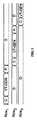
図1は、従来の電圧プログラムAMOLEDディスプレイのための従来的な動作サイクルを図解している。図1において『Rowi』(i=1,2,3)は、AMOLEDディスプレイのi番目の行のマトリクス・ピクセル・アレイを表す。図1において『C』は、ピクセル回路の駆動トランジスタのゲート‐ソース端子間にわたって補償電圧が現れる補償電圧生成サイクルを表し、『VT‐GEN』は、駆動トランジスタのスレッショルド電圧VTが生成されるVT生成サイクルを表し、『P』は、駆動トランジスタのゲートに対してプログラミング電圧を印加することによってピクセル電流のレギュレーションが行われる電流レギュレーション・サイクルを表し、『D』は、駆動トランジスタによりコントロールされた電流によってピクセル回路のOLEDが駆動される駆動サイクルを表す。FIG. 1 illustrates a conventional operating cycle for a conventional voltage programmed AMOLED display. In FIG. 1, “Rowi” (i = 1, 2, 3) represents the matrix pixel array of the i-th row of the AMOLED display. In FIG. 1, “C” represents a compensation voltage generation cycle in which a compensation voltage appears between the gate and source terminals of the drive transistor of the pixel circuit, and “VT-GEN” represents V V at which the threshold voltage VT of the drive transistor is generated.T represents theT generation cycle, “P” represents a current regulation cycle in which the pixel current is regulated by applying a programming voltage to the gate of the driving transistor, and “D” was controlled by the driving transistor. It represents a driving cycle in which an OLED of a pixel circuit is driven by a current.
AMOLEDディスプレイの各行について、動作サイクルが、補償電圧生成サイクル『C』、VT生成サイクル『VT‐GEN』、電流レギュレーション・サイクル『P』、および駆動サイクル『D』を含む。通常、これらの動作サイクルが、図1に示されるとおり、マトリクス構造についてシーケンシャルに実行される。たとえば、第1行(すなわち、Row1)の全プログラミング・サイクル(すなわち『C』、『VT‐GEN』、および『P』)が実行され、その後、第2行(すなわち、Row2)がプログラムされる。For each row in the AMOLED display, operation cycle, compensation voltage generation cycle "C",V T generated cycle "VT-GEN", the current regulation cycle "P", and a driving cycle "D". Typically, these operating cycles are performed sequentially for the matrix structure, as shown in FIG. For example, the entire programming cycle (ie, “C”, “VT-GEN”, and “P”) of the first row (ie, Row1 ) is executed, and then the second row (ie, Row2 ) is programmed. Is done.
しかしながら、VT生成サイクル『VT‐GEN』が、駆動TFTの正確なスレッショルド電圧の生成に大きな時間配分を必要とすることから、このタイミング・スケジュールが大面積ディスプレイで採用できない。さらに、2つの余分な動作サイクル(すなわち『C』および『VT‐GEN』)の実行が、結果としてより大きな電力消費をもたらし、さらに余分なコントロール信号を必要として、それがより高い実装コストを招く。However, VT generated cycle "VT-GEN" is because it requires a large allocation of time to produce accurate threshold voltage of the driving TFT, the timing schedule can not be employed in large area displays. In addition, execution of two extra operating cycles (ie, “C” and “VT-GEN”) results in more power consumption and requires extra control signals, which incur higher implementation costs. .
本発明は、既存のシステムの欠点の少なくとも1つを回避するか、または緩和する方法およびシステムを提供することを目的とする。 The present invention seeks to provide a method and system that avoids or mitigates at least one of the disadvantages of existing systems.
本発明の態様によれば、行および列で配列された複数のピクセル回路を含むピクセル・アレイを含むディスプレイ・システムが提供される。ピクセル回路は、発光デバイス、キャパシタ、スイッチ・トランジスタ、および発光デバイスを駆動するための駆動トランジスタを有する。ピクセル回路は、プログラミングのためのパス、および駆動トランジスタのスレッショルドを生成するための第2のパスを含む。このシステムは、ピクセル・アレイにプログラミングのためのデータを提供するための第1のドライバ、および1つまたは複数の駆動トランジスタのための駆動トランジスタのスレッショルドの生成をコントロールするための第2のドライバを含む。第1のドライバおよび第2のドライバは、ピクセル・アレイを駆動してプログラミングおよび生成動作を独立に実行する。 According to an aspect of the invention, a display system is provided that includes a pixel array that includes a plurality of pixel circuits arranged in rows and columns. The pixel circuit has a light emitting device, a capacitor, a switch transistor, and a driving transistor for driving the light emitting device. The pixel circuit includes a pass for programming and a second pass for generating a threshold for the drive transistor. The system includes a first driver for providing data for programming to the pixel array, and a second driver for controlling generation of drive transistor thresholds for the one or more drive transistors. Including. The first driver and the second driver drive the pixel array to perform programming and generation operations independently.
本発明の別の態様によれば、ディスプレイ・システムを駆動する方法が提供される。ディスプレイ・システムは、行および列で配列された複数のピクセル回路を含むピクセル・アレイを含む。ピクセル回路は、発光デバイス、キャパシタ、スイッチ・トランジスタ、および発光デバイスを駆動するための駆動トランジスタを有する。ピクセル回路は、プログラミングのためのパス、および駆動トランジスタのスレッショルドを生成するための第2のパスを含む。この方法は、1つまたは複数の駆動トランジスタのための駆動トランジスタのスレッショルドの生成をコントロールするステップ、そのコントロールするステップとは独立に、ピクセル・アレイにプログラミングのためのデータを提供するステップを含む。 In accordance with another aspect of the present invention, a method for driving a display system is provided. The display system includes a pixel array that includes a plurality of pixel circuits arranged in rows and columns. The pixel circuit has a light emitting device, a capacitor, a switch transistor, and a driving transistor for driving the light emitting device. The pixel circuit includes a pass for programming and a second pass for generating a threshold for the drive transistor. The method includes controlling generation of drive transistor thresholds for one or more drive transistors, and providing the pixel array with data for programming independent of the controlling step.
本発明の追加の態様によれば、行および列で配列された複数のピクセル回路を含むピクセル・アレイを含むディスプレイ・システムが提供される。ピクセル回路は、発光デバイス、キャパシタ、スイッチ・トランジスタ、および発光デバイスを駆動するための駆動トランジスタを有する。このシステムは、ピクセル・アレイにプログラミングのためのデータを提供するための第1のドライバ、および行内の各ピクセル回路の老化ファクタを生成し、対応するピクセル回路内にストアするための第2のドライバを含み、複数のフレームのための行内のピクセル回路のプログラミングおよび駆動は、ストアされた老化ファクタに基づく。ピクセル・アレイは、複数のセグメントに分割される。老化ファクタを生成するための第2のドライバによって駆動される信号ラインのうちの少なくとも1つは、セグメント内において共有される。 According to an additional aspect of the present invention, a display system is provided that includes a pixel array that includes a plurality of pixel circuits arranged in rows and columns. The pixel circuit has a light emitting device, a capacitor, a switch transistor, and a driving transistor for driving the light emitting device. The system includes a first driver for providing data for programming to the pixel array, and a second driver for generating an aging factor for each pixel circuit in the row and storing it in the corresponding pixel circuit. The programming and driving of pixel circuits in a row for multiple frames is based on the stored aging factor. The pixel array is divided into a plurality of segments. At least one of the signal lines driven by the second driver for generating the aging factor is shared within the segment.
本発明の追加の態様によれば、ディスプレイ・システムを駆動する方法が提供される。ディスプレイ・システムは、行および列で配列された複数のピクセル回路を含むピクセル・アレイを含む。ピクセル回路は、発光デバイス、キャパシタ、スイッチ・トランジスタ、および発光デバイスを駆動するための駆動トランジスタを有する。ピクセル・アレイは、複数のセグメントに分割される。この方法は、各行について、セグメント信号を使用して各ピクセル回路の老化ファクタを生成し、老化ファクタを対応するピクセル回路内にストアするステップ、およびセグメント信号が各セグメントによって共有されること、およびストアされた老化ファクタに基づいて複数のフレームについて行内のピクセル回路をプログラムし、駆動するステップを含む。 According to an additional aspect of the present invention, a method for driving a display system is provided. The display system includes a pixel array that includes a plurality of pixel circuits arranged in rows and columns. The pixel circuit has a light emitting device, a capacitor, a switch transistor, and a driving transistor for driving the light emitting device. The pixel array is divided into a plurality of segments. The method includes, for each row, generating an aging factor for each pixel circuit using the segment signal and storing the aging factor in the corresponding pixel circuit, and that the segment signal is shared by each segment, and storing Programming and driving the pixel circuits in the row for a plurality of frames based on the determined aging factor.
本発明のこの要約は、必ずしも本発明のすべての特徴を述べているわけではない。 This summary of the invention does not necessarily describe all features of the invention.
本発明のこれらの、およびこのほかの特徴は、以下の添付図面を参照した説明からより明らかなものとなろう。 These and other features of the present invention will become more apparent from the following description with reference to the accompanying drawings.
本発明の実施態様を、行および列に配列されてAMOLEDディスプレイを形成する有機発光ダイオード(OLED)等の発光デバイスおよび薄膜トランジスタ(TFT)等の複数のトランジスタを有するピクセル回路を使用して説明する。ピクセル回路は、OLED用のピクセル・ドライバを含むことができる。しかしながら、ピクセルがOLED以外のいずれかの発光デバイスを含むこともでき、またピクセルがTFT以外のいずれかのトランジスタを含むこともできる。ピクセル回路内のトランジスタは、n型トランジスタ、p型トランジスタ、またはそれらの組み合わせとすることができる。ピクセル内のトランジスタは、アモルファス・シリコン、ナノ/マイクロ結晶質シリコン、ポリ・シリコン、有機半導体テクノロジ(たとえば有機TFT)、NMOS/PMOSテクノロジまたはCMOSテクノロジ(たとえば、MOSFET)を使用して製造できる。説明においては、『ピクセル回路』および『ピクセル』が相互交換可能に使用されることがある。ピクセル回路は、電流プログラム・ピクセルまたは電圧プログラム・ピクセルとすることができる。以下の説明においては、『信号』および『ライン』が相互交換可能に使用されることがある。 Embodiments of the invention are described using a light emitting device such as an organic light emitting diode (OLED) arranged in rows and columns to form an AMOLED display and a pixel circuit having a plurality of transistors such as thin film transistors (TFTs). The pixel circuit can include a pixel driver for the OLED. However, the pixel can include any light emitting device other than an OLED, and the pixel can include any transistor other than a TFT. The transistors in the pixel circuit can be n-type transistors, p-type transistors, or a combination thereof. The transistors in the pixel can be manufactured using amorphous silicon, nano / microcrystalline silicon, poly silicon, organic semiconductor technology (eg organic TFT), NMOS / PMOS technology or CMOS technology (eg MOSFET). In the description, “pixel circuit” and “pixel” may be used interchangeably. The pixel circuit can be a current program pixel or a voltage program pixel. In the following description, “signal” and “line” may be used interchangeably.
本発明の実施態様は、駆動TFTの正確なスレッショルド電圧を生成するためのテクニックを伴う。結果としてこれは、たとえばピクセルの老化、および処理の変動に起因するピクセル・エレメントの特性のシフトに抗して安定した電流を生成する。これは、OLEDの輝度の安定性を強化する。またこれは、電力消費および信号を低減し、結果として低い実装コストをもたらす。 Embodiments of the present invention involve techniques for generating an accurate threshold voltage for the drive TFT. As a result, this produces a stable current against pixel element characteristic shifts due to, for example, pixel aging and process variations. This enhances the luminance stability of the OLED. This also reduces power consumption and signal, resulting in lower implementation costs.
セグメント化されたタイミング・スケジュールおよび並列タイミング・スケジュールを詳細に説明する。これらのスケジュールは、駆動トランジスタのスレッショルド電圧VTを生成するためのサイクルの時間配分を拡張する。以下において説明するとおり、ディスプレイ・アレイ内の行はセグメント化され、動作サイクルは、複数のカテゴリ、たとえば2カテゴリに分割される。たとえば、第1のカテゴリが補償サイクルおよびVT生成サイクルを含み、第2のカテゴリが電流レギュレーション・サイクルおよび駆動サイクルを含む。各カテゴリのための動作サイクルは、各セグメントについてシーケンシャルに実行されるが、2つのカテゴリは、2つの隣接するセグメントについて実行される。たとえば、電流レギュレーションおよび駆動サイクルが第1のセグメントについてシーケンシャルに実行されている間、補償およびVT生成サイクルが第2のセグメントについて実行される。The segmented timing schedule and parallel timing schedule will be described in detail. These schedules extend the time distribution of the cycles to generate the drive transistor threshold voltage VT. As described below, the rows in the display array are segmented and the operating cycle is divided into multiple categories, for example two categories. For example, the first category includes compensation cycles andVT generation cycles, and the second category includes current regulation cycles and drive cycles. The operating cycle for each category is performed sequentially for each segment, while the two categories are performed for two adjacent segments. For example, compensation andVT generation cycles are performed for the second segment while current regulation and drive cycles are performed sequentially for the first segment.
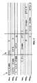
図2は、本発明の実施態様に従った、発光ディスプレイの安定した動作のためのセグメント化されたタイミング・スケジュールの例を図解している。図2において『Rowk』(k=1,2,3,...,j,j+1,j+2)は、ディスプレイ・アレイ内のk番目の行を表し、矢印は、実行方向を示している。FIG. 2 illustrates an example of a segmented timing schedule for stable operation of a light emitting display according to an embodiment of the present invention. In FIG. 2, “Rowk ” (k = 1, 2, 3,..., J, j + 1, j + 2) represents the kth row in the display array, and the arrows indicate the execution direction.
各行について、図2のタイミング・スケジュールは、補償電圧生成サイクル『C』、VT生成サイクル『VT‐GEN』、電流レギュレーション・サイクル『P』、および駆動サイクル『D』を含む。
For each row, the timing schedule of Figure 2, compensation voltage generation cycle "C", VT generated cycle "VT-GEN", the current regulation cycle"P", and a driving cycle"D".
図2のタイミング・スケジュールは、プログラミング時間に影響を与えることなくVT生成サイクル『VT‐GEN』の時間配分を拡張する。これを達成するために、図2のセグメント化されたアドレシング・スキームが適用されるディスプレイ・アレイの行がいくつかのセグメントとしてカテゴリ分けされる。各セグメントは、したがって、VT生成サイクルが実行される行を含む。図2においてRow1、Row2、Row3、...Rowjは、ディスプレイ・アレイの複数の行内の1つのセグメント内にある。Timing schedule of Figure 2, to extend the time distribution of VT generated cycle "VT-GEN" without affecting the programming time. To accomplish this, the rows of the display array to which the segmented addressing scheme of FIG. 2 is applied are categorized as several segments. Each segment thus comprises a row of VT generated cycle is executed. In FIG. 2, Row1 , Row2 , Row3 ,. . . Rowj is in one segment in multiple rows of the display array.
各セグメントのプログラミングは、1番目および2番目の動作サイクル『C』および『VT‐GEN』の実行を伴って開始する。その後、電流較正サイクル『P』がそのセグメント全体について実行される。その結果としてVT生成サイクル『VT‐GEN』の時間配分が、j.τPまで拡張され、それにおいてjは各セグメント内の行の数であり、τPは、1番目の動作サイクル『C』(または電流レギュレーション・サイクル)の時間配分である。The programming of each segment begins with the execution of the first and second operating cycles “C” and “VT-GEN”. A current calibration cycle “P” is then performed for the entire segment. As a resultV T time distribution of the product cycle "VT-GEN" is, j. extended to τP , where j is the number of rows in each segment, and τP is the time distribution of the first operating cycle “C” (or current regulation cycle).
また、フレーム時間τFは、Z×n×τPであり、それにおいてnはディスプレイ内の行の数、Zはセグメント内の反復回数の関数である。たとえば、図2においては、VT生成が、セグメントの第1行から開始して最後の行に至り(1番目の反復)、その後プログラミングが第1行から開始して最後の行に至る(2番目の反復)。したがって、Zが2にセットされる。反復回数が増加すると、フレーム時間がZ×n×τPになり、それにおいてZは反復回数であり、2より大きくなることがある。Also, the frame time τF is Z × n × τP , where n is the number of rows in the display and Z is a function of the number of iterations in the segment. For example, in FIG. 2,VT generation starts from the first line of the segment to the last line (first iteration), and then programming starts from the first line to the last line (2 Th iteration). Therefore, Z is set to 2. When the number of iterations increases, the frame time becomes Z × n × τP, Z is a number of iterations in which, may be greater than 2.
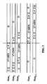
図3は、本発明の実施態様に従った、発光ディスプレイの安定した動作のための並列タイミング・スケジュールの例を図解している。図3において『Rowk』(k=1,2,3,...,j,j+1)は、ディスプレイ・アレイ内のk番目の行を表す。FIG. 3 illustrates an example of a parallel timing schedule for stable operation of a light emitting display according to an embodiment of the present invention. In FIG. 3, “Rowk ” (k = 1, 2, 3,..., J, j + 1) represents the k th row in the display array.
図2と同様に、図4のタイミング・スケジュールは、各行について補償電圧生成サイクル『C』、VT生成サイクル『VT‐GEN』、電流レギュレーション・サイクル『P』、および駆動サイクル『D』を含む。Similar to FIG. 2, the timing schedule of Figure 4, each row for compensation voltage generation cycle "C", VT generated cycle "VT-GEN", the current regulation cycle "P", and a driving cycle "D" .
図3のタイミング・スケジュールは、VT生成サイクル『VT‐GEN』の時間配分を拡張するが、τPがτF/nとして保存され、それにおいてτPは1番目の動作サイクル『C』の時間配分であり、τFはフレーム時間、nはディスプレイ・アレイ内の行の数である。図3において、Row1〜Rowjは、ディスプレイ・アレイの複数の行内のセグメント内にある。Timing schedule of FIG. 3, but extends the time allocation of the VT generated cycle "VT-GEN", tauP is stored as τF / n, τP is the first operating cycle of the "C" in it Time allocation, τF is the frame time, and n is the number of rows in the display array. In FIG. 3, Row1 to Rowj are in segments in multiple rows of the display array.
上記のアドレシング・スキームによれば、各セグメントの電流レギュレーション・サイクル『P』が、次のセグメントの1番目の動作サイクル『C』と並列に実行される。このようにこのディスプレイ・アレイは、並列動作をサポートするべく設計され、すなわち互いに影響を及ぼし合うことなく異なるサイクルを、たとえば補償およびプログラミング、VT生成および電流レギュレーションを独立に実行する能力を有する。According to the above addressing scheme, the current regulation cycle “P” of each segment is executed in parallel with the first operating cycle “C” of the next segment. Thus, the display array is designed to support parallel operation, i.e., has the ability to independently perform different cycles, such as compensation and programming,VT generation and current regulation, without affecting each other.
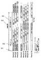
図4は、図2および3のタイミング・スケジュールのためのAMOLEDディスプレイ・アレイ構造の例を図解している。図4においてSEL[a](a=1,...,m)は、行を選択する選択信号を表し、CTRL[b](b=1,...,m)は、行内の各ピクセルにおいて駆動TFTのスレッショルド電圧を生成するコントロール信号を表し、VDATA[c](c=1,...,n)は、プログラミング・データを提供するデータ信号を表す。図4のAMOLEDディスプレイ10は、行および列で配列された複数のピクセル回路12、SEL[a]およびCTRL[b]をコントロールするためのアドレス・ドライバ14、およびVDATA[c]をコントロールするためのデータ・ドライバ16を含む。ピクセル回路12の行(たとえばRow1,...,Rowm‐h,Rowm‐h+1,...,Rowm)は、上記のとおりにセグメント化される。特定のサイクルを並列に実行するために、AMOLEDディスプレイ10は、並列動作をサポートするべく設計されている。FIG. 4 illustrates an example of an AMOLED display array structure for the timing schedule of FIGS. In FIG. 4, SEL [a] (a = 1,..., M) represents a selection signal for selecting a row, and CTRL [b] (b = 1,..., M) represents each pixel in the row. Represents a control signal for generating a threshold voltage of the driving TFT, and VDATA [c] (c = 1,..., N) represents a data signal for providing programming data. The
図5は、セグメント化されたタイミング・スケジュールおよび並列タイミング・スケジュールが適用できるピクセル回路の例を図解している。図5のピクセル回路50は、OLED 52、ストレージ・キャパシタ54、駆動TFT 56、およびスイッチTFT 58および60を含む。選択ラインSEL1がスイッチTFT 58のゲート端子に接続されている。選択ラインSEL2がスイッチTFT 60のゲート端子に接続されている。スイッチTFT 58の第1の端子は、データ・ラインVDATAに接続され、スイッチTFT 58の第2の端子は、ノードA1において駆動TFT 56のゲートに接続される。スイッチTFT 60の第1の端子は、ノードA1に接続され、スイッチTFT 60の第2の端子は、グラウンド・ラインに接続される。駆動TFT 56の第1の端子は、コントロール可能な電圧源VDDに接続され、駆動TFT 56の第2の端子は、ノードB1においてOLED 52のアノード電極に接続される。ストレージ・キャパシタ54の第1の端子は、ノードA1に接続され、ストレージ・キャパシタ54の第2の端子は、ノードB1に接続される。ピクセル回路50は、セグメント化されたタイミング・スケジュール、並列タイミング・スケジュール、およびそれらの組み合わせとともに使用可能である。 FIG. 5 illustrates an example of a pixel circuit to which a segmented timing schedule and a parallel timing schedule can be applied. The
VT生成は、トランジスタ56および60を通じて生じ、一方、電流レギュレーションは、トランジスタ58によりVDATAラインを通じて実行される。したがって、このピクセルは、並列動作を実装できる。VT generation occurs through
図6は、ピクセル回路50に適用されるタイミング・スケジュールの例を図解している。図7において『X11』、『X12』、『X13』、および『X14』は、動作サイクルを表す。X11は図2および3の『C』に対応し、X12は図2および3の『VT‐GEN』に対応し、X13は図2および3の『P』に対応し、X14は図2および3の『D』に対応する。 FIG. 6 illustrates an example of a timing schedule applied to the
図5および6を参照するとストレージ・キャパシタ54は、1番目の動作サイクルX11の間に負の電圧(‐Vcomp)まで充電され、その間、駆動TFT 56のゲート電圧はゼロである。2番目の動作サイクルX12の間には、ノードB1が‐VTまで充電され、それにおいてVTは駆動TFT 56のスレッショルドである。このサイクルX12は、それがスイッチ・トランジスタ60を介して実行され、スイッチ・トランジスタ58を介さないことからデータ・ラインVDATAに影響を及ぼすことなく実行可能であり、その結果、別の行のための別の行の動作サイクルを実行することが可能になる。3番目の動作サイクルX13の間に、ノードA1がプログラミング電圧VPまで充電され、結果としてVGS=VP+VTが得られ、それにおいてVGSは、駆動TFT 56のゲート‐ソース電圧を表す。5 and 6, the
図7は、セグメント化されたタイミング・スケジュールおよび並列タイミング・スケジュールが適用できるピクセル回路の別の例を図解している。図7のピクセル回路70は、OLED 72、ストレージ・キャパシタ74および76、駆動TFT 78、およびスイッチTFT 80、82、および84を含む。第1の選択ラインSEL1が、スイッチTFT 80および82のゲート端子に接続されている。第2の選択ラインSEL2が、スイッチTFT 84のゲート端子に接続されている。スイッチTFT 80の第1の端子は、OLED 72のカソードに接続され、スイッチTFT 80の第2の端子は、ノードA2において駆動TFT 78のゲート端子に接続される。スイッチTFT 82の第1の端子は、ノードB2に接続され、スイッチTFT 82の第2の端子は、グラウンド・ラインに接続される。スイッチTFT 84の第1の端子は、データ・ラインVDATAに接続され、スイッチTFT 84の第2の端子は、ノードB2に接続される。ストレージ・キャパシタ74の第1の端子は、ノードA2に接続され、ストレージ・キャパシタ74の第2の端子は、ノードB2に接続される。ストレージ・キャパシタ76の第1の端子は、ノードB2に接続され、ストレージ・キャパシタ76の第2の端子は、グラウンド・ラインに接続される。駆動TFT 78の第1の端子は、OLED 72のカソード電極に接続され、駆動TFT 78の第2の端子は、グラウンド・ラインに結合される。OLED 72のアノード電極は、コントロール可能な電圧源VDDに結合される。ピクセル回路70は、セグメント化されたタイミング・スケジュール、並列タイミング・スケジュール、およびそれらの組み合わせを採用することができる。 FIG. 7 illustrates another example of a pixel circuit to which a segmented timing schedule and a parallel timing schedule can be applied. The
VT生成は、トランジスタ78、80、および82を通じて生じ、一方、電流レギュレーションは、トランジスタ84によりVDATAラインを通じて実行される。したがって、このピクセルは、並列動作を実装できる。VT generation occurs through
図8は、ピクセル回路70に適用されるタイミング・スケジュールの例を図解している。図8において『X21』、『X22』、『X23』、および『X24』は、動作サイクルを表す。 FIG. 8 illustrates an example of a timing schedule applied to the
X21は図2および3の『C』に対応し、X22は図2および3の『VT‐GEN』に対応し、X23は図2および3の『P』に対応し、X24は図2および3の『D』に対応する。 X21 corresponds to “C” in FIGS. 2 and 3, X22 corresponds to “VT-GEN” in FIGS. 2 and 3, X23 corresponds to “P” in FIGS. 2 and 3, and X24 corresponds to “P” in FIGS. Corresponds to “D”.
図7および8を参照すると、ピクセル回路70は、蓄積VTに対するプログラミング電圧の追加にブートストラップ効果を採用しており、それにおいてVTは、駆動TFT 78のスレッショルド電圧である。1番目の動作サイクルx21の間に、ノードA2が補償電圧VDD‐VOLEDまで充電され、ノードB2がグラウンドまで放電されるが、それにおいてVOLEDは、OLED 72の電圧である。2番目の動作サイクルX22の間に、ノードA2における電圧が駆動TFT 78のVTまで変化される。電流レギュレーションは、3番目の動作サイクルX23の間に生じ、その間にノードB2がプログラミング電圧VPまで充電され、その結果、ノードA2がVP+VTまで変化する。With reference to FIGS. 7 and 8, the
前述したセグメント化されたタイミング・スケジュールおよび並列タイミング・スケジュールは、ピクセル回路が駆動TFTの正確なスレッショルド電圧を生成するための充分な時間を提供する。その結果として、ピクセルの老化、処理の変動、またはそれらの組み合わせに抗して安定した電流が生成される。動作サイクルは、セグメント内の1つの行のプログラミング・サイクルに、そのセグメント内の別の行のプログラミング・サイクルがオーバーラップするようにセグメント内において共有される。したがって、高い表示速度を、ディスプレイのサイズとは無関係に維持できる。 The segmented timing schedule and parallel timing schedule described above provide sufficient time for the pixel circuit to generate the correct threshold voltage of the drive TFT. As a result, a stable current is generated against pixel aging, process variations, or combinations thereof. An operating cycle is shared within a segment such that the programming cycle of one row in the segment overlaps the programming cycle of another row in that segment. Therefore, a high display speed can be maintained regardless of the display size.
共有シグナリング・アドレシング・スキームを詳細に説明する。共有シグナリング・アドレシング・スキームによれば、ディスプレイ・アレイ内の行が、いくつかのセグメントに分割される。ピクセル回路の老化ファクタ(たとえば、駆動TFTのスレッショルド電圧、OLED電圧)はピクセル内にストアされる。ストアされている老化ファクタは、複数のフレームのために使用される。老化ファクタの生成に必要な1またはそれより多くの信号は、そのセグメント内において共有される。 The shared signaling addressing scheme will be described in detail. According to the shared signaling addressing scheme, the rows in the display array are divided into several segments. The aging factor of the pixel circuit (e.g., drive TFT threshold voltage, OLED voltage) is stored in the pixel. Stored aging factors are used for multiple frames. One or more signals required to generate an aging factor are shared within the segment.
たとえば、駆動TFTのスレッショルド電圧VTは、同時に各セグメント用に生成される。その後、そのセグメントが正常な動作に置かれる。スレッショルド電圧の生成に必要なデータ・ラインおよび選択ラインを除くすべての余分な信号は(たとえば、図10のVSS)、各セグメント内の行の間において共有される。TFTの漏れ電流が小さいとすれば、妥当なストレージ・キャパシタを使用したVTの蓄積は、より頻繁でない補償サイクルに帰結する。その結果、電力消費が劇的に低減する。For example, the threshold voltage VT of the driving TFT is generated for each segment at the same time. The segment is then put into normal operation. All extra signals except the data lines and select lines needed to generate the threshold voltage (eg, VSS in FIG. 10) are shared between the rows in each segment. If the leakage current of the TFT is small, the accumulation of VT using reasonable storage capacitor results in compensation cycle a less frequent. As a result, power consumption is dramatically reduced.
各セグメントについてVT生成サイクルが行われることから、VT生成サイクルに割り当てられる時間がセグメント内の行数倍に拡張され、より精密な補償をもたらす。a‐Si:TFTの漏れ電流が小さい(たとえば10‐14台)ことから、生成されたVTをキャパシタ内に蓄積し、ほかのいくつかのフレームに使用することができる。その結果、次の後補償フレームの間の動作サイクルがプログラミングおよび駆動サイクルに還元される。したがって、外部ドライバに、および寄生キャパシタンスの充電/放電に関連付けされる電力消費が同じいくつかのフレームの間で分割される。Since aVT generation cycle is performed for each segment, the time allotted to theVT generation cycle is extended to the number of rows in the segment, resulting in more precise compensation. Since the leakage current of the a-Si: TFT is small (for example, 10−14 units), the generated VT can be stored in the capacitor and used for some other frames. As a result, the operating cycle during the next post-compensation frame is reduced to the programming and driving cycle. Thus, the power consumption associated with the external driver and the charging / discharging of the parasitic capacitance is divided between the same several frames.
図9は、本発明の実施態様に従った発光ディスプレイのための共有シグナリング・アドレシング・スキームの例を図解している。共有シグナリング・アドレシング・スキームは、インターフェースおよびドライバの複雑性を低減する。 FIG. 9 illustrates an example of a shared signaling addressing scheme for a light emitting display according to an embodiment of the present invention. A shared signaling addressing scheme reduces interface and driver complexity.
共有シグナリング・アドレシング・スキームが適用されるディスプレイ・アレイは、図2および3についての場合と同様にいくつかのセグメントに分割される。図9において、『Row[j,k]』(k=1,2,3,...,h)は、j番目のセグメント内のk番目の行を表し、『h』は各セグメント内の行の数であり、『L』は、同一の生成済みVTを使用するフレームの数である。図9において、『Row[j,k]』(k=1,2,3,...,h)は1つのセグメント内であり、『Row[j‐1,k]』(k=1,2,3,...,h)は別のセグメント内である。The display array to which the shared signaling addressing scheme is applied is divided into several segments as in FIGS. In FIG. 9, “Row [j, k]” (k = 1, 2, 3,..., H) represents the k th row in the j th segment, and “h” represents in each segment. the number of rows, "L" is the number of frames using the same of the generated VT. In FIG. 9, “Row [j, k]” (k = 1, 2, 3,..., H) is in one segment, and “Row [j−1, k]” (k = 1, 2, 3, ..., h) are in another segment.
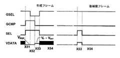
図9のタイミング・スケジュールは補償サイクル『C & VT‐GEN』(たとえば、図9の301)、プログラミング・サイクル『P』、および駆動サイクル『D』を含む。補償区間300は、駆動TFTのスレッショルド電圧が生成されてピクセル内に蓄積される生成フレーム・サイクル302、補償サイクル『C & VT‐GEN』(たとえば、図9の301)をディスプレイの通常の動作のほかに、および通常の動作フレームであるL‐1個の後補償フレーム・サイクル304を含む。生成フレーム・サイクル302は、1つのプログラミング・サイクル『P』および1つの駆動サイクル『D』を含む。L‐1個の後補償フレーム・サイクル304は、プログラミング・サイクル『P』および駆動サイクル『D』のセットを直列に含む。 The timing schedule of FIG. 9 includes a compensation cycle “C & VT-GEN” (eg, 301 in FIG. 9), a programming cycle “P”, and a driving cycle “D”. The
図9に示されているとおり、各行の駆動サイクルは、直前の行からτPの遅延を伴って開始し、τPはプログラミング・サイクル『P』に割り当てられた時間配分である。最後のフレームにおける駆動サイクル『D』のタイミングは、各行について、i×τPだけ縮小され、それにおいて『i』は、そのセグメント内のその行に先行する行の数である(たとえば、Row[j,h]の場合は(h‐1))。As shown in FIG. 9, the drive cycle for each row starts with a delay of τP from the previous row, where τP is the time allocation assigned to programming cycle “P”. The timing of the drive cycle “D” in the last frame is reduced by i × τP for each row, where “i” is the number of rows preceding that row in the segment (eg, Row [ In the case of j, h], (h-1)).
τP(たとえば10μs台)がフレーム時間(たとえば16ms台)よりはるかに小さいことから、遅れ時間の効果は無視できる。しかしながら、この効果を最小化するため、遅れ時間に起因する平均輝度の損失がすべての行にわたって等しくなるように、その都度プログラミング方向を変更するか、この効果を、補償サイクルの前および後のフレームのプログラミング電圧において考慮する。たとえば、行のプログラミングのシーケンスを各VT生成サイクルの後に変更する(すなわち、上から下と、下から上に向かうプログラミングを反復する)。Since τP (for example, 10 μs) is much smaller than the frame time (for example, 16 ms), the effect of the delay time can be ignored. However, to minimize this effect, either change the programming direction each time so that the average luminance loss due to lag time is equal across all rows, or this effect can be applied to frames before and after the compensation cycle. Consider the programming voltage. For example, the row programming sequence is changed after eachVT generation cycle (ie, top-to-bottom and bottom-to-top programming is repeated).
図10は、共有シグナリング・アドレシング・スキームが適用できるピクセル回路の例を図解している。図10のピクセル回路90は、OLED 92、ストレージ・キャパシタ94および96、駆動TFT 98、およびスイッチTFT 100、102、および104を含む。このピクセル回路90は、図7のピクセル回路70に類似である。駆動TFT 98、スイッチTFT 100、および第1のストレージ・キャパシタ94は、ノードA3において接続される。スイッチTFT 102および104、および第1および第2のストレージ・キャパシタ94および96は、ノードB3において接続される。OLED 92、駆動TFT 98、およびスイッチTFT 100は、ノードC3において接続される。スイッチTFT 102、第2のストレージ・キャパシタ96、および駆動TFT 98は、コントロール可能な電圧源VSSに接続される。 FIG. 10 illustrates an example of a pixel circuit to which a shared signaling addressing scheme can be applied. The
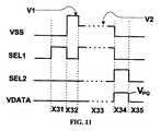
図11は、ピクセル回路90に適用されるタイミング・スケジュールの例を図解している。図11において、『X31』、『X32』、『X33』、『X34』、および『X35』は、動作サイクルを表す。 FIG. 11 illustrates an example of a timing schedule applied to the
X31、X32、およびX33は、補償サイクル(たとえば図9の301)に対応し、X34は、図9の『P』に対応し、X35は図9の『D』に対応する。 X31, X32, and X33 correspond to a compensation cycle (for example, 301 in FIG. 9), X34 corresponds to “P” in FIG. 9, and X35 corresponds to “D” in FIG.
図10および11を参照すると、ピクセル回路90は、生成済みVTに対するプログラミング電圧の追加にブートストラップ効果を採用しており、それにおいてVTは、駆動TFT 98のスレッショルド電圧である。補償サイクル(たとえば図9の301)は、最初の3サイクルX31、X32、およびX33を含む。1番目の動作サイクルX31の間に、ノードA3が補償電圧VDD‐VOLEDまで充電される。1番目の動作サイクルX31のタイミングは、不要な放射の効果をコントロールするために小さい。2番目の動作サイクルX32の間に、VSSが高い正電圧V1(たとえば、V1=20V)まで上昇し、したがってノードA3が高い電圧にブートストラップされ、またノードC3もV1まで上昇し、その結果としてOLED 92をオフにする。3番目の動作サイクルX33の間に、ノードA3の電圧がスイッチTFT 100および駆動TFT 98を通じて放電されてV2+VTに落ち着くが、それにおいてVTは駆動TFT 98のスレッショルド電圧であり、V2は、たとえば16ボルトである。VSSは、電流レギュレーション・サイクルの前にゼロになり、ノードA3はVTになる。プログラミング電圧VPGが、4番目の動作サイクルX34の間にブートストラップによって生成済みのVTに追加される。電流レギュレーションは、4番目の動作サイクルX34内に生じ、その間にノードB3がプログラミング電圧VPG(たとえば、VPG=6V)まで充電される。したがって、ノードA3における電圧がVPG+VTに変化し、結果としてVTとは独立のオーバードライブ電圧をもたらす。5番目のサイクルX35(駆動サイクル)の間のピクセル回路の電流は、VTのシフトと独立になる。ここでは、VT生成区間の間のVTの蓄積に第1のストレージ・キャパシタ94が使用される。Referring to FIGS. 10 and 11, the
図12は、図10のピクセル回路90のピクセル電流の安定性を図解している。図12において『ΔVT』は、駆動TFT(たとえば、図10の98)のスレッショルド電圧におけるシフトを表し、『lpixel内誤差(%)』は、ΔVTによって引き起こされるピクセル電流内の変化を表す。図12に示されているとおり、図10のピクセル回路90は、駆動TFTのVT内における2Vのシフトの後でさえ、高度に安定した電流を提供する。FIG. 12 illustrates the pixel current stability of the
図13は、共有シグナリング・アドレシング・スキームが適用できるピクセル回路の別の例を図解している。図13のピクセル回路110は、図10のピクセル回路90に類似であるが、2つのスイッチTFTを含む。ピクセル回路110は、OLED 112、ストレージ・キャパシタ114および116、駆動TFT 118、およびスイッチTFT 120および122を含む。駆動TFT 118、スイッチTFT 120、および第1のストレージ・キャパシタ114は、ノードA4において接続される。スイッチTFT 122および第1および第2のストレージ・キャパシタ114および116は、ノードB4において接続される。OLED 112のカソード、駆動TFT 118、およびスイッチTFT 120は、ノードC4において接続される。第2のストレージ・キャパシタ116および駆動TFT 118は、コントロール可能な電圧源VSSに接続される。 FIG. 13 illustrates another example of a pixel circuit to which a shared signaling addressing scheme can be applied. The
図14は、ピクセル回路110に適用されるタイミング・スケジュールの例を図解している。図15において、『X41』、『X42』、『X43』、『X44』、および『X44』は、動作サイクルを表す。X41、X42、およびX43は、補償サイクル(たとえば図9の301)に対応し、X44は、図9の『P』に対応し、X45は図9の『D』に対応する。 FIG. 14 illustrates an example of a timing schedule applied to the
図13および14を参照すると、ピクセル回路110は、生成済みVTに対するプログラミング電圧の追加にブートストラップ効果を採用している。補償サイクル(たとえば図9の301)は、最初の3サイクルX41、X42、およびX43を含む。1番目の動作サイクルX41の間に、ノードA4が補償電圧VDD‐VOLEDまで充電される。1番目の動作サイクルX41のタイミングは、不要な放射の効果をコントロールするために小さい。2番目の動作サイクルX42の間に、VSSが高い正電圧V1(たとえば、V1=20V)まで上昇し、したがってノードA4が高い電圧にブートストラップされ、またノードC4もV1まで上昇し、その結果としてOLED 112をオフにする。3番目の動作サイクルX43の間に、ノードA4の電圧がスイッチTFT 120および駆動TFT 118を通じて放電されてV2+VTに落ち着くが、それにおいてVTは駆動TFT 118のスレッショルド電圧であり、V2は、たとえば16ボルトである。VSSは、電流レギュレーション・サイクルの前にゼロになり、ノードA4はVTになる。プログラミング電圧VPGが、4番目の動作サイクルX44の間にブートストラップによって生成済みのVTに追加される。電流レギュレーションは、4番目の動作サイクルX44内に生じ、その間にノードB4がプログラミング電圧VPG(たとえば、VPG=6V)まで充電される。したがって、ノードA4における電圧がVPG+VTに変化し、結果としてVTとは独立のオーバードライブ電圧をもたらす。5番目のサイクルX45(駆動サイクル)の間のピクセル回路の電流は、VTのシフトと独立になる。ここでは、VT生成区間の間のVTの蓄積に第1のストレージ・キャパシタ114が使用される。Referring to FIGS. 13 and 14, the
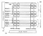
図15は、図10のピクセル回路のためのAMOLEDディスプレイ構造の例を図解している。図15において、GSEL[a](a=1,...,k)は図10のSEL2に対応し、SEL1[b](b=1,...,m)は図10のSEL1に対応し、GVSS[c](c=1,...,k)図10のVSSに対応し、VDATA[d](d=1,...,n)は図10のVDATAに対応する。図15のAMOLEDディスプレイ200は、行および列で配列された複数のピクセル回路90、GSEL[a]、SEL1[b]、およびGVSS[c]をコントロールするためのアドレス・ドライバ204、およびVDATA[s]をコントロールするためのデータ・ドライバ206を含む。ピクセル回路90の行は、前述のとおりにセグメント化される。図15には、例としてセグメント[1]およびセグメント[k]が示されている。 FIG. 15 illustrates an example of an AMOLED display structure for the pixel circuit of FIG. 15, GSEL [a] (a = 1,..., K) corresponds to SEL2 in FIG. 10, and SEL1 [b] (b = 1,..., M) corresponds to SEL1 in FIG. GVSS [c] (c = 1,..., K) corresponds to VSS in FIG. 10, and VDATA [d] (d = 1,..., N) corresponds to VDATA in FIG. The
図10および15を参照すると、1つのセグメント内の行のSEL2およびVSS信号が互いに接続されてGSELおよびGVSS信号を形成している。 Referring to FIGS. 10 and 15, the SEL2 and VSS signals of the rows in one segment are connected together to form the GSEL and GVSS signals.
図16は、図14のピクセル回路のためのAMOLEDディスプレイ構造の例を図解している。図17において、GSEL[a](a=1,...,k)は図14のSEL2に対応し、SEL1[b](b=1,...,m)は図14のSEL1に対応し、GVSS[c](c=1,...,k)図14のVSSに対応し、VDATA[d](d=1,...,n)は図14のVDATAに対応する。図16のAMOLEDディスプレイ210は、行および列で配列された複数のピクセル回路110、GSEL[a]、SEL1[b]、およびGVSS[c]をコントロールするためのアドレス・ドライバ214、およびVDATA[s]をコントロールするためのデータ・ドライバ216を含む。ピクセル回路110の行は、前述のとおりにセグメント化される。図15には、例としてセグメント[1]およびセグメント[k]が示されている。 FIG. 16 illustrates an example of an AMOLED display structure for the pixel circuit of FIG. 17, GSEL [a] (a = 1,..., K) corresponds to SEL2 in FIG. 14, and SEL1 [b] (b = 1,..., M) corresponds to SEL1 in FIG. GVSS [c] (c = 1,..., K) corresponds to VSS in FIG. 14, and VDATA [d] (d = 1,..., N) corresponds to VDATA in FIG. The
図14および16を参照すると、1つのセグメント内の行のSEL2およびVSS信号が互いに接続されてGSELおよびGVSS信号を形成している。 Referring to FIGS. 14 and 16, the SEL2 and VSS signals of the rows in one segment are connected together to form the GSEL and GVSS signals.
図15および16を参照すると、このディスプレイ・アレイは、物理的に隣接する行の間においてVSSおよびGSEL信号を共有することによってその面積を減少させることができる。それに加えて、同一セグメント内のGVSSおよびGSELが併合されてセグメントGVSSおよびGSELラインが形成される。したがって、コントロール信号が低減される。さらに、信号を駆動するブロックの数もまた低減され、より低い電力消費およびより低い実装コストがもたらされる。 Referring to FIGS. 15 and 16, the display array can reduce its area by sharing VSS and GSEL signals between physically adjacent rows. In addition, GVSS and GSEL within the same segment are merged to form segment GVSS and GSEL lines. Therefore, the control signal is reduced. Furthermore, the number of blocks driving the signal is also reduced, resulting in lower power consumption and lower implementation costs.
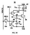
図17は、共有シグナリング・アドレシング・スキームが適用できるピクセル回路のさらに別の例を図解している。図17のピクセル回路は、OLED 132、ストレージ・キャパシタ134および136、駆動TFT 138、およびスイッチTFT 140、142、および144を含む。第1の選択ラインSELが、スイッチTFT 142のゲート端子に接続される。第2の選択ラインGSELが、スイッチTFT 144のゲート端子に接続される。GCOMP信号ラインが、スイッチTFT 140のゲート端子に接続される。スイッチTFT 140の第1の端子は、ノードA5に接続され、スイッチTFT 140の第2の端子は、ノードC5に接続される。駆動TFT 138の第1の端子は、ノードC5に接続され、駆動TFT 138の第2の端子は、OLED 132のアノードに接続される。スイッチTFT 142の第1の端子は、データ・ラインVDATAに接続され、スイッチTFT 142の第2の端子は、ノードB5に接続される。スイッチTFT 144の第1の端子は、電圧源VDDに接続され、スイッチTFT 144の第2の端子は、ノードC5に接続される。第1のストレージ・キャパシタ134の第1の端子は、ノードA5に接続され、第1のストレージ・キャパシタ134の第2の端子は、ノードB5に接続される。第2のストレージ・キャパシタ136の第1の端子は、ノードB5に接続され、第2のストレージ・キャパシタ136の第2の端子は、VDDに接続される。 FIG. 17 illustrates yet another example of a pixel circuit to which a shared signaling addressing scheme can be applied. The pixel circuit of FIG. 17 includes
図18は、ピクセル回路130に適用されるタイミング・スケジュールの例を図解している。図18において、動作サイクルX51、X52、X53、およびX54は、生成フレーム・サイクル(たとえば図9の302)を形成し、2番目の動作サイクルX53およびX54は、後補償フレーム・サイクル(たとえば図9の304)を形成する。X53およびX54は、通常の動作サイクルであるが、残りは補償サイクルである。 FIG. 18 illustrates an example of a timing schedule applied to the
図17および18を参照すると、ピクセル回路130は、生成済みVTに対するプログラミング電圧の追加にブートストラップ効果を採用しており、それにおいてVTは、駆動TFT 138のスレッショルド電圧である。補償サイクル(たとえば図9の301)は、最初の2サイクルX51およびX52を含む。1番目の動作サイクルX51の間に、ノードA5が補償電圧まで充電され、ノードB5が、スイッチTFT 142およびVDATAを介してVREFまで充電される。1番目の動作サイクルX51のタイミングは、不要な放射の効果をコントロールするために小さい。2番目の動作サイクルX52の間にGSELがゼロになり、したがってスイッチTFT 144をオフにする。ノードA5の電圧はスイッチTFT 140および駆動TFT 138を介して放電されてVOLED+VTに落ち着くが、それにおいてVOLEDはOLED 132の電圧であり、VTは駆動TFT 138のスレッショルド電圧である。プログラミング・サイクルの間、すなわち3番目の動作サイクルX53の間に、ノードB5がVP+VREFまで充電されるが、それにおいてVPはプログラミング電圧である。したがって、駆動TFT 138のゲート電圧がVOLED+VT+VPになる。ここでは、補償区間の間のVT+VOLEDの蓄積に第1のストレージ・キャパシタ134が使用される。Referring to FIGS. 17 and 18, the
図19は、図17のピクセル回路130のためのAMOLEDディスプレイ・アレイ構造の例を図解している。図19においてGSEL[a](a=1,...,k)は、図17のGSELに対応し、SEL[b](b=1,...,m)は、図17のSEL1に対応し、GCMP[c](c=1,...,k)は、図17のGCOMPに対応し、VDATA[d](d=1,...,n)は、図17のVDATAに対応する。図19のAMOLEDディスプレイ220は、行および列で配列された複数のピクセル回路130、SEL[a]、GSEL[b]、およびGCOMP[c]をコントロールするためのアドレス・ドライバ224、およびVDATA[c]をコントロールするためのデータ・ドライバ226を含む。ピクセル回路130の行は、前述のとおりにセグメント化される(たとえば、セグメント[1]およびセグメント[k])。 FIG. 19 illustrates an example of an AMOLED display array structure for the
図17および19に示されているとおり、1つのセグメント内の行のGSELおよびGCOMP信号が互いに接続されてGSELおよびGCOMPラインを形成している。GSELおよびGCOMP信号は、そのセグメント内において共有される。それに加えて、同一セグメント内のGVSSおよびGSELが併合されてセグメントGVSSおよびGSELラインが形成される。したがって、コントロール信号が低減される。さらに、信号を駆動するブロックの数もまた低減され、より低い電力消費およびより低い実装コストがもたらされる。 As shown in FIGS. 17 and 19, the GSEL and GCOMP signals of the rows in one segment are connected together to form the GSEL and GCOMP lines. The GSEL and GCOMP signals are shared within that segment. In addition, GVSS and GSEL within the same segment are merged to form segment GVSS and GSEL lines. Therefore, the control signal is reduced. Furthermore, the number of blocks driving the signal is also reduced, resulting in lower power consumption and lower implementation costs.
図20は、共有アドレシング・スキームが適用できるピクセル回路のさらに別の例を図解している。図20のピクセル回路150は、図17のピクセル回路130に類似である。ピクセル回路150は、OLED 152、ストレージ・キャパシタ154および156、駆動TFT 158、およびスイッチTFT 160、162、および164を含む。スイッチTFT 164のゲート端子は、GSELではなくコントロール可能な電圧源VDDに接続される。駆動TFT 158、スイッチTFT 162、および第1のストレージ・キャパシタ154は、ノードA6に接続される。スイッチTFT 162および第1および第2のストレージ・キャパシタ154および156は、ノードB6に接続される。駆動TFT 158およびスイッチTFT 160および164は、ノードC6に接続される。 FIG. 20 illustrates yet another example of a pixel circuit to which a shared addressing scheme can be applied. The
図21は、ピクセル回路150に適用されるタイミング・スケジュールの例を図解している。図21において、動作サイクルX61、X62、X63、およびX64は、生成フレーム・サイクル(たとえば図9の302)を形成し、2番目の動作サイクルX63およびX64は、後補償フレーム・サイクル(たとえば図9の304)を形成する。 FIG. 21 illustrates an example of a timing schedule applied to the
図20および21を参照すると、ピクセル回路150は、生成済みVTに対するプログラミング電圧の追加にブートストラップ効果を採用しており、それにおいてVTは、駆動TFT 158のスレッショルド電圧である。補償サイクル(たとえば図9の301)は、最初の2サイクルX61およびX62を含む。1番目の動作サイクルX61の間に、ノードA6が補償電圧まで充電され、ノードB6が、スイッチTFT 162およびVDATAを介してVREFまで充電される。1番目の動作サイクルx61のタイミングは、不要な放射の効果をコントロールするために小さい。2番目の動作サイクルx62の間にVDDがゼロになり、したがってスイッチTFT 164をオフにする。ノードA6の電圧はスイッチTFT 160および駆動TFT 158を介して放電されてVOLED+VTに落ち着くが、それにおいてVOLEDはOLED 152の電圧であり、VTは駆動TFT 158のスレッショルド電圧である。プログラミング・サイクルの間、すなわち3番目の動作サイクルx63の間に、ノードB6がVP+VREFまで充電されるが、それにおいてVPはプログラミング電圧である。駆動TFT 158のゲート電圧がVOLED+VT+VPとなることが明らかにされた。ここでは、補償区間の間のVT+VOLEDの蓄積に第1のストレージ・キャパシタ154が使用される。Referring to FIGS. 20 and 21, the
図22は、図20のピクセル回路150のためのAMOLEDディスプレイ・アレイ構造の例を図解している。図22においてSEL[a](a=1,...,m)は、図22のSELに対応し、GCMP[b](b=1,...,K)は、図22のGCOMPに対応し、GVDD[c](c=1,...,k)は、図22のVDDに対応し、VDATA[d](d=1,...,n)は、図22のVDATAに対応する。図22のAMOLEDディスプレイ230は、行および列で配列された複数のピクセル回路150、SEL[a]、GCOMP[b]、およびGVDD[c]をコントロールするためのアドレス・ドライバ234、およびVDATA[c]をコントロールするためのデータ・ドライバ236を含む。ピクセル回路230の行は、前述のとおりにセグメント化される(たとえば、セグメント[1]およびセグメント[k])。 FIG. 22 illustrates an example of an AMOLED display array structure for the
図20および22を参照すると、1つのセグメント内の行のVDDおよびGCOMP信号が互いに接続されてGVDDおよびGCOMPラインを形成している。GVDDおよびGCOMP信号は、そのセグメント内において共有される。それに加えて、同一セグメント内のGVDDおよびGCOMPが併合されてセグメントGVDDおよびGCOMPラインが形成される。したがって、コントロール信号が低減される。さらに、信号を駆動するブロックの数もまた低減され、より低い電力消費およびより低い実装コストがもたらされる。 Referring to FIGS. 20 and 22, the VDD and GCOMP signals of rows within a segment are connected together to form the GVDD and GCOMP lines. The GVDD and GCOMP signals are shared within that segment. In addition, GVDD and GCOMP in the same segment are merged to form segment GVDD and GCOMP lines. Therefore, the control signal is reduced. Furthermore, the number of blocks driving the signal is also reduced, resulting in lower power consumption and lower implementation costs.
本発明の実施態様によれば、動作サイクルがセグメント内で共有され、駆動TFTの正確なスレッショルド電圧が生成される。これは電力消費および信号を低減し、結果としてより低い実装コストをもたらす。 According to an embodiment of the present invention, the operating cycle is shared within the segment, and an accurate threshold voltage of the driving TFT is generated. This reduces power consumption and signal, resulting in lower implementation costs.
セグメント内の1つの行の動作サイクルは、そのセグメント内の別の行の動作サイクルとオーバーラップされる。したがって、高い表示速度を、ディスプレイのサイズとは無関係に維持できる。 The operating cycle of one row in a segment is overlapped with the operating cycle of another row in that segment. Therefore, a high display speed can be maintained regardless of the display size.
生成されるVTの精度は、VT生成サイクルに割り付けられる時間に依存する。生成されるVTは、ストレージ・キャパシタンスおよび駆動TFTのパラメータの関数であり、その結果として特殊な不整合が、駆動トランジスタの所定のスレッショルド電圧のためのストレージ・キャパシタ内の不整合の中で関連付けされる影響を生成されるVTに及ぼす。VT生成サイクルの時間の増加は、生成されるVTに対するその特殊な不整合の効果を低減する。本発明の実施態様によれば、フレーム・レートに影響を与えること、または行数を低減することのいずれも伴わずにVTに割り当てられるタイミングの拡張が可能であり、したがって不完全な補償および空間的不整合の効果を、パネルのサイズとは無関係に低減することができる。VT accuracy produced depends on the time allocated to VT generated cycle. The generated VT is a function of storage capacitance and drive TFT parameters, so that a special mismatch is associated with the mismatch in the storage capacitor for a given threshold voltage of the drive transistor. Affects the generated VT. Increased time of VT generation cycle, reduces the effect of the special mismatch for VT generated. According to an embodiment of the present invention, it can affect the frame rate, but may be extended timing assigned to VT without any of reducing or row number, thus incomplete compensation and The effect of spatial misalignment can be reduced regardless of panel size.
VT生成時間が増加されて、駆動TFTのゲート‐ソース端子間にわたるそのスレッショルド電圧VTの高精度リカバリを可能にする。その結果としてパネル全体の一様性が向上する。それに加えて、アドレシング・スキームのためのピクセル回路は、ピクセルの老化に従って、予測可能な、より高い電流を提供することが可能であり、それによりOLEDの輝度の低下を補償する。VT generation time is increased, the gate of the driving TFT - enables accurate recovery of its threshold voltage VT across between the source terminal. As a result, the uniformity of the entire panel is improved. In addition, the pixel circuit for the addressing scheme can provide a predictable higher current as the pixel ages, thereby compensating for the decrease in brightness of the OLED.
本発明の実施態様によれば、アドレシング・スキームが、バックプレーンの安定性を改善し、またOLEDの輝度の低下も補償する。電力消費および実装コストにおけるオーバーヘッドは、既存の補償駆動スキームと比較して90%超低減される。 According to an embodiment of the present invention, the addressing scheme improves backplane stability and also compensates for OLED brightness degradation. The overhead in power consumption and implementation costs is reduced by more than 90% compared to existing compensation drive schemes.
共有アドレシング・スキームが低い電力消費を保証することから、モバイル応用等の低電力応用に向いている。モバイル応用は、限定ではないが携帯情報端末(PDA)、携帯電話等とすることができる。 Since the shared addressing scheme ensures low power consumption, it is suitable for low power applications such as mobile applications. Mobile applications can include, but are not limited to, personal digital assistants (PDAs), mobile phones, and the like.
すべての引例は、参照によってこれに援用される。 All references are hereby incorporated by reference.
以上、1または複数の実施態様に関連して本発明を説明してきた。しかしながら、当業者には明らかであろうが、請求項内に定義されている本発明の範囲から逸脱することなしに多くの変形および修正を行うことが可能である。 The invention has been described with reference to one or more embodiments. However, it will be apparent to those skilled in the art that many variations and modifications can be made without departing from the scope of the invention as defined in the claims.
10 AMOLEDディスプレイ、12 ピクセル回路、14 アドレス・ドライバ、16 データ・ドライバ、50 ピクセル回路、52 OLED、54 ストレージ・キャパシタ、56 駆動TFT;トランジスタ、58 スイッチTFT;トランジスタ;スイッチ・トランジスタ、60 スイッチTFT;トランジスタ;スイッチ・トランジスタ、70 ピクセル回路、72 OLED、74 ストレージ・キャパシタ、76 ストレージ・キャパシタ、78 駆動TFT、80 スイッチTFT、82 スイッチTFT、84 スイッチTFT、90 ピクセル回路、92 OLED、94 ストレージ・キャパシタ、96 ストレージ・キャパシタ、98 駆動TFT、100 スイッチTFT、102 スイッチTFT、104 スイッチTFT、110 ピクセル回路、112 OLED、114 ストレージ・キャパシタ、116 ストレージ・キャパシタ、118 駆動TFT、120 スイッチTFT、122 スイッチTFT、130 ピクセル回路、132 OLED、134 ストレージ・キャパシタ、136 ストレージ・キャパシタ、138 駆動TFT、140 スイッチTFT、142 スイッチTFT、144 スイッチTFT、150 ピクセル回路、152 OLED、154 ストレージ・キャパシタ、156 ストレージ・キャパシタ、158 駆動TFT、160 スイッチTFT、162 スイッチTFT、164 スイッチTFT、200 AMOLEDディスプレイ、204 アドレス・ドライバ、206 データ・ドライバ、210 AMOLEDディスプレイ、214 アドレス・ドライバ、216 データ・ドライバ、220 AMOLEDディスプレイ、224 アドレス・ドライバ、226 データ・ドライバ、230 AMOLEDディスプレイ、234 アドレス・ドライバ、236 データ・ドライバ、300 補償区間、302 生成フレーム・サイクル、304 後補償フレーム・サイクル。 10 AMOLED display, 12 pixel circuit, 14 address driver, 16 data driver, 50 pixel circuit, 52 OLED, 54 storage capacitor, 56 drive TFT; transistor, 58 switch TFT; transistor; switch transistor, 60 switch TFT; Transistor: switch transistor, 70 pixel circuit, 72 OLED, 74 storage capacitor, 76 storage capacitor, 78 drive TFT, 80 switch TFT, 82 switch TFT, 84 switch TFT, 90 pixel circuit, 92 OLED, 94 storage capacitor , 96 Storage capacitor, 98 Drive TFT, 100 Switch TFT, 102 Switch TFT, 104 Switch TFT 110 pixel circuit, 112 OLED, 114 storage capacitor, 116 storage capacitor, 118 drive TFT, 120 switch TFT, 122 switch TFT, 130 pixel circuit, 132 OLED, 134 storage capacitor, 136 storage capacitor, 138 drive TFT , 140 switch TFT, 142 switch TFT, 144 switch TFT, 150 pixel circuit, 152 OLED, 154 storage capacitor, 156 storage capacitor, 158 drive TFT, 160 switch TFT, 162 switch TFT, 164 switch TFT, 200 AMOLED display, 204 address driver, 206 data driver, 210 AMOLED display , 214 Address Driver, 216 Data Driver, 220 AMOLED Display, 224 Address Driver, 226 Data Driver, 230 AMOLED Display, 234 Address Driver, 236 Data Driver, 300 Compensation Interval, 302 Generated Frame Cycle, 304 Post-compensation frame cycle.
Claims (18)
Translated fromJapanese複数のピクセル回路を含むとともに、複数のセグメントに分割され、各セグメントが複数行の複数のピクセルを含むピクセルアレイであって、各ピクセル回路は、発光デバイスと、前記発光デバイスを駆動して発光させるための駆動トランジスタと、キャパシタと、前記ピクセル回路をプログラミングするためにデータ・ラインに接続された第1スイッチ・トランジスタと、前記駆動トランジスタのスレッショルド電圧を発生するための第2スイッチ・トランジスタとを含むピクセルアレイと、
プログラミング動作中に前記第1スイッチ・トランジスタを、データを受けるように制御するとともに、スレッショルド電圧発生動作中に前記第2スイッチ・トランジスタを、前記駆動トランジスタのスレッショルド電圧を発生するように制御するドライバと、
を含み、
前記ドライバは、前記ピクセルアレイにおける2以上の行のピクセル回路であって、前記複数のセグメントの中の第1セグメントの2以上の行のピクセル回路において、前記スレッショルド電圧発生動作を同時に実行させる一方、前記複数のセグメントの第2セグメントのピクセル回路において駆動動作またはプログラミング動作を実行させ、
前記ドライバは、第2セグメントのいかなる行についてスレッショルド電圧発生動作を行わせる前に、第1セグメントにおける少なくとも2行についてプログラムさせる、
ディスプレイ・システム。A display system,
A pixel array including a plurality of pixel circuits and divided into a plurality of segments, each segment including a plurality of rows of pixels, each pixel circuit driving a light emitting device and the light emitting device to emit light A drive transistor for coupling, a capacitor, a first switch transistor connected to a data line for programming the pixel circuit, and a second switch transistor for generating a threshold voltage of the drive transistor. A pixel array;
A driver controlling the first switch transistor to receive data during a programming operation and controlling the second switch transistor to generate a threshold voltage of the driving transistor during a threshold voltage generating operation; ,
Including
The driver is a pixel circuit of two or more rows in the pixel array, and the threshold voltage generation operation is simultaneously performed in the pixel circuit of two or more rows of the first segment in the plurality of segments, A driving operation or a programming operation is performed in a pixel circuit of a second segment of the plurality of segments;
The driver causes at least two rows in the first segment to be programmed before performing the threshold voltage generation operation for any row in the second segment.
Display system.
前記複数のピクセル回路のそれぞれは、さらに、
第2キャパシタと、第3スイッチ・トランジスタを含み、
前記複数のピクセル回路のそれぞれでは、第1スイッチ・トランジスタのゲート端子が第1選択ラインに接続されており、第2および第3スイッチ・トランジスタのゲート端子が、第2選択ラインに接続され、
第1および第2選択ラインは、前記ドライバによって駆動され、
第1スイッチ・トランジスタの第1端子が前記データ・ラインに接続され、第1スイッチ・トランジスタの第2端子は前記第1キャパシタの第2端子および第2キャパシタの第1端子に接続され、
前記第2スイッチ・トランジスタの第1端子が第1スイッチ・トランジスタの第2端子に接続され、前記第2スイッチ・トランジスタの第2端子がグランドに接続され、
第3スイッチ・トランジスタの第1端子が駆動トランジスタの第1端子および発光デバイスの第2端子に接続され、
駆動トランジスタの第2端子がグランドに接続され、発光デバイスの第1端子が電源に接続され、
第3スイッチ・トランジスタの第2端子が駆動トランジスタのゲート端子に接続され、
前記第1キャパシタの第1端子が前記駆動トランジスタのゲート端子に接続され、前記第1キャパシタの第2端子が前記第2キャパシタの第1端子に接続され、前記第2キャパシタの第2端子がグランドに接続される、請求項1に記載のディスプレイ・システム。Each of the plurality of pixel circuits includes a first capacitor as the capacitor,
Each of the plurality of pixel circuits further includes
A second capacitor and a third switch transistor;
In each of the plurality of pixel circuits, the gate terminal of the first switch transistor is connected to the first selection line, and the gate terminals of the second and third switch transistors are connected to the second selection line,
The first and second selection lines are driven by the driver,
The first terminal of the first switch transistor being connected to said data line, a second terminal of the first switch transistor is connected to afirst terminal of thesecond terminal and the second capacitorof the firstcapacitor,
A first terminal of the second switch transistoris connected to a second terminal of the first switch transistor; a second terminal of the second switch transistor is connected toground ;
A first terminal of the third switch transistor is connected to a first terminal of the driving transistor anda second terminal of thelight emitting device ;
The second terminal of the driving transistor is connected to ground, the first terminal of the light emitting device is connected to the power source,
The second terminal of the third switch transistor is connected to the gate terminal of the drive transistor;
Thefirst terminal of thefirst key Yapashita isconnected to the gate terminal of the drivingtransistor, the second terminal of the first capacitor is connected to the first terminal of the second capacitor, a second terminal of said second capacitor There Ruis connected to the ground, a display system according to claim 1.
前記ディスプレイ・システムは、
複数のピクセル回路を含むとともに、複数のセグメントに分割され、各セグメントが複数行の複数のピクセルを含むピクセルアレイであって、各ピクセル回路は、発光デバイスと、前記発光デバイスを駆動して発光させるための駆動トランジスタと、キャパシタと、前記ピクセル回路をプログラミングするためにデータ・ラインに接続された第1スイッチ・トランジスタと、前記駆動トランジスタのスレッショルド電圧を発生するための第2スイッチ・トランジスタとを含むピクセルアレイ、
を含むとともに、
前記方法が、
前記ピクセルアレイの2以上の行の複数のピクセル回路における第2トランジスタを制御し、複数のセグメントの中の第1セグメントの各ピクセル回路に、前記データ・ラインを操作することなく、前記ピクセル回路の中の前記駆動トランジスタのスレッショルド電圧を同時に発生させるように制御するとともに、
前記第1セグメントのピクセル回路の第2スイッチ・トランジスタの制御から独立して、前記第2セグメントのピクセル回路の第1スイッチ・トランジスタを制御して前記第2セグメントのピクセル回路をプログラムする、
方法。A method for driving a display system, comprising:
The display system is
A pixel array including a plurality of pixel circuits and divided into a plurality of segments, each segment including a plurality of rows of pixels, each pixel circuit driving a light emitting device and the light emitting device to emit light A drive transistor for coupling, a capacitor, a first switch transistor connected to a data line for programming the pixel circuit, and a second switch transistor for generating a threshold voltage of the drive transistor. Pixel array,
Including
The method comprises
The second transistor in the plurality of pixel circuits in two or more rows of the pixel array is controlled so that each pixel circuit of the first segment in the plurality of segments has the pixel circuit without operating the data line. And controlling to generate the threshold voltage of the driving transistor in the same simultaneously,
Independent of controlling the second switch transistor of the pixel circuit of the first segment, controlling the first switch transistor of the pixel circuit of the second segment to program the pixel circuit of the second segment;
Method.
請求項7に記載の方法。Each segment includes a first plurality of rows, and control of the second switch transistor is performed sequentially for each segment in the plurality of segments.
The method of claim 7.
請求項1に記載のディスプレイ・システム。At least one of the transistors is amorphous silicon, nano / microcrystalline silicon, poly silicon, organic semiconductor including organic transistors, NMOS / PMOS or CMOS technology including MOSFET, p-type material, or n-type material Manufactured using,
The display system according to claim 1.
請求項1に記載のディスプレイ・システム。The drive transistor or thelight emitting device is connected to a voltage controllable line by the driver to precharge the capacitor of the pixel circuit during a first phase of generating a threshold voltage.
The display system according to claim 1.
請求項1に記載のディスプレイ・システム。In each pixel circuit, the capacitor is connected between a gate terminal of the driving transistor and thelight emitting device .
The display system according to claim 1.
前記複数のピクセル回路のそれぞれは、
前記キャパシタとして、第1端子および第2端子を有する第1キャパシタであって、前記第1端子が前記駆動トランジスタのゲート端子に接続されている、第1キャパシタを有し、
前記複数のピクセル回路のそれぞれは、前記第1キャパシタの第2端子に接続される第1端子と、1つの電位に接続される第2端子を有する第2キャパシタをさらに含み、
前記第1スイッチ・トランジスタは、前記第2キャパシタの第1端子および第1キャパシタの第2端子に接続されている、
ディスプレイ・システム。The display system of claim 1.
Each of the plurality of pixel circuits includes
The capacitor includes a first capacitor having a first terminal and a second terminal, wherein the first terminal is connected to a gate terminal of the driving transistor;
Each of the plurality of pixel circuits further includes a second capacitor having a first terminal connected to the second terminal of the first capacitor and a second terminal connected to one potential.
The first switch transistor is connected to a first terminal of the second capacitor and a second terminal of the first capacitor;
Display system.
前記第2スイッチ・トランジスタ、第3スイッチ・トランジスタおよび前記駆動トランジスタが、前記駆動トランジスタのスレッショルド電圧を発生する回路を形成する、
ディスプレイ・システム。The display system according to claim 6, comprising:
The second switch transistor, the third switch transistor and the drive transistor form a circuit for generating a threshold voltage of the drive transistor;
Display system.
第1セグメントにおける前記第2スイッチ・トランジスタの制御および前記第1スイッチ・トランジスタの制御は、前記第2セグメントにおいて、前記第2スイッチ・トランジスタの制御および第1スイッチ・トランジスタの制御が実行された後に、行われる、
方法。The method of claim 7, comprising:
The control of the second switch transistor and the control of the first switch transistor in the first segment are performed after the control of the second switch transistor and the control of the first switch transistor are executed in the second segment. Done,
Method.
前記第2セグメントにおいて前記第2スイッチ・トランジスタの制御が行われている間に、前記第1セグメントにおいて前記第2スイッチ・トランジスタの制御が行われる、
方法。The method of claim 7, comprising:
While the second switch transistor is controlled in the second segment, the second switch transistor is controlled in the first segment.
Method.
前記ドライバは、
前記第1セグメントにおける複数のピクセル回路の前記スレッショルド電圧が発生されている間に、前記第2セグメントのピクセル回路を駆動して光を射出させる、
ディスプレイ・システム。The display system according to claim 1, comprising:
The driver is
Driving the pixel circuit of the second segment to emit light while the threshold voltage of the plurality of pixel circuits in the first segment is generated;
Display system.
第2セグメントにおけるピクセル回路のプログラミングと並行して第1セグメントにおける複数のピクセル回路についての前記スレッショルド電圧を発生するように第2スイッチ・トランジスタの制御が行われる、
方法。The method of claim 7, comprising:
The second switch transistor is controlled to generate the threshold voltage for the plurality of pixel circuits in the first segment in parallel with the programming of the pixel circuits in the second segment.
Method.
さらに、
第2セグメントにおけるピクセル回路の駆動と並行して、第1セグメントにおける複数のピクセル回路の前記スレッショルド電圧の発生が行われるように、前記第1セグメントにおける複数のピクセル回路の第2トランジスタの制御が行われる間に、
前記第2セグメントの第2ピクセル回路を駆動して光を射出させる、
方法。
The method of claim 7, comprising:
further,
In parallel with the driving of the pixel circuits in the second segment, the second transistors of the plurality of pixel circuits in the first segment are controlled so that the threshold voltages of the plurality of pixel circuits in the first segment are generated. While
Driving the second pixel circuit of the second segment to emit light;
Method.
Applications Claiming Priority (7)
| Application Number | Priority Date | Filing Date | Title |
|---|---|---|---|
| CA2,508,972 | 2005-06-08 | ||
| CA002508972ACA2508972A1 (en) | 2005-06-08 | 2005-06-08 | New timing schedule for stable operation of amoled displays |
| CA002537173ACA2537173A1 (en) | 2006-02-20 | 2006-02-20 | Low-power low-cost driving scheme for mobile applications |
| CA2,537,173 | 2006-02-20 | ||
| CA2,542,678 | 2006-04-10 | ||
| CA002542678ACA2542678A1 (en) | 2006-04-10 | 2006-04-10 | Amoled display for mobile applications |
| PCT/CA2006/000941WO2006130981A1 (en) | 2005-06-08 | 2006-06-08 | Method and system for driving a light emitting device display |
Related Child Applications (1)
| Application Number | Title | Priority Date | Filing Date |
|---|---|---|---|
| JP2013138321ADivisionJP2013190829A (en) | 2005-06-08 | 2013-07-01 | Method and system for driving light emitting device display |
Publications (2)
| Publication Number | Publication Date |
|---|---|
| JP2008542845A JP2008542845A (en) | 2008-11-27 |
| JP5355080B2true JP5355080B2 (en) | 2013-11-27 |
Family
ID=37498080
Family Applications (4)
| Application Number | Title | Priority Date | Filing Date |
|---|---|---|---|
| JP2008515013AExpired - Fee RelatedJP5355080B2 (en) | 2005-06-08 | 2006-06-08 | Method and system for driving a light emitting device display |
| JP2013138321APendingJP2013190829A (en) | 2005-06-08 | 2013-07-01 | Method and system for driving light emitting device display |
| JP2014133475AExpired - Fee RelatedJP6207472B2 (en) | 2005-06-08 | 2014-06-30 | Method and system for driving a light emitting device display |
| JP2014154749AWithdrawnJP2014240972A (en) | 2005-06-08 | 2014-07-30 | Method and system for driving light emitting device display |
Family Applications After (3)
| Application Number | Title | Priority Date | Filing Date |
|---|---|---|---|
| JP2013138321APendingJP2013190829A (en) | 2005-06-08 | 2013-07-01 | Method and system for driving light emitting device display |
| JP2014133475AExpired - Fee RelatedJP6207472B2 (en) | 2005-06-08 | 2014-06-30 | Method and system for driving a light emitting device display |
| JP2014154749AWithdrawnJP2014240972A (en) | 2005-06-08 | 2014-07-30 | Method and system for driving light emitting device display |
Country Status (7)
| Country | Link |
|---|---|
| US (5) | US7852298B2 (en) |
| EP (1) | EP1904995A4 (en) |
| JP (4) | JP5355080B2 (en) |
| KR (1) | KR20080032072A (en) |
| CN (1) | CN102663977B (en) |
| TW (1) | TW200707376A (en) |
| WO (1) | WO2006130981A1 (en) |
Cited By (1)
| Publication number | Priority date | Publication date | Assignee | Title |
|---|---|---|---|---|
| US9330598B2 (en) | 2005-06-08 | 2016-05-03 | Ignis Innovation Inc. | Method and system for driving a light emitting device display |
Families Citing this family (87)
| Publication number | Priority date | Publication date | Assignee | Title |
|---|---|---|---|---|
| CA2443206A1 (en) | 2003-09-23 | 2005-03-23 | Ignis Innovation Inc. | Amoled display backplanes - pixel driver circuits, array architecture, and external compensation |
| EP1825455A4 (en)* | 2004-11-16 | 2009-05-06 | Ignis Innovation Inc | System and driving method for active matrix light emitting device display |
| CA2490858A1 (en) | 2004-12-07 | 2006-06-07 | Ignis Innovation Inc. | Driving method for compensated voltage-programming of amoled displays |
| US10013907B2 (en) | 2004-12-15 | 2018-07-03 | Ignis Innovation Inc. | Method and system for programming, calibrating and/or compensating, and driving an LED display |
| US9799246B2 (en) | 2011-05-20 | 2017-10-24 | Ignis Innovation Inc. | System and methods for extraction of threshold and mobility parameters in AMOLED displays |
| US8576217B2 (en) | 2011-05-20 | 2013-11-05 | Ignis Innovation Inc. | System and methods for extraction of threshold and mobility parameters in AMOLED displays |
| US9489891B2 (en) | 2006-01-09 | 2016-11-08 | Ignis Innovation Inc. | Method and system for driving an active matrix display circuit |
| US9269322B2 (en) | 2006-01-09 | 2016-02-23 | Ignis Innovation Inc. | Method and system for driving an active matrix display circuit |
| WO2007079572A1 (en) | 2006-01-09 | 2007-07-19 | Ignis Innovation Inc. | Method and system for driving an active matrix display circuit |
| TW200746022A (en) | 2006-04-19 | 2007-12-16 | Ignis Innovation Inc | Stable driving scheme for active matrix displays |
| CA2556961A1 (en) | 2006-08-15 | 2008-02-15 | Ignis Innovation Inc. | Oled compensation technique based on oled capacitance |
| JP4300491B2 (en)* | 2007-03-13 | 2009-07-22 | ソニー株式会社 | Display device |
| JP5287111B2 (en)* | 2007-11-14 | 2013-09-11 | ソニー株式会社 | Display device, driving method thereof, and electronic apparatus |
| EP2277163B1 (en)* | 2008-04-18 | 2018-11-21 | Ignis Innovation Inc. | System and driving method for light emitting device display |
| CA2637343A1 (en) | 2008-07-29 | 2010-01-29 | Ignis Innovation Inc. | Improving the display source driver |
| JP5214384B2 (en)* | 2008-09-26 | 2013-06-19 | 株式会社東芝 | Display device and driving method thereof |
| US9370075B2 (en) | 2008-12-09 | 2016-06-14 | Ignis Innovation Inc. | System and method for fast compensation programming of pixels in a display |
| KR101269000B1 (en)* | 2008-12-24 | 2013-05-29 | 엘지디스플레이 주식회사 | Organic electro-luminescent display device and driving method thereof |
| JP5580536B2 (en)* | 2009-01-09 | 2014-08-27 | グローバル・オーエルイーディー・テクノロジー・リミテッド・ライアビリティ・カンパニー | Display device |
| WO2010087420A1 (en)* | 2009-01-30 | 2010-08-05 | Fujifilm Corporation | Driving of oled display device with interleaving of control phases |
| US10319307B2 (en) | 2009-06-16 | 2019-06-11 | Ignis Innovation Inc. | Display system with compensation techniques and/or shared level resources |
| US9384698B2 (en) | 2009-11-30 | 2016-07-05 | Ignis Innovation Inc. | System and methods for aging compensation in AMOLED displays |
| US9311859B2 (en) | 2009-11-30 | 2016-04-12 | Ignis Innovation Inc. | Resetting cycle for aging compensation in AMOLED displays |
| KR20110013693A (en) | 2009-08-03 | 2011-02-10 | 삼성모바일디스플레이주식회사 | Organic electroluminescent display and driving method thereof |
| KR101056281B1 (en) | 2009-08-03 | 2011-08-11 | 삼성모바일디스플레이주식회사 | Organic electroluminescent display and driving method thereof |
| US8497828B2 (en) | 2009-11-12 | 2013-07-30 | Ignis Innovation Inc. | Sharing switch TFTS in pixel circuits |
| JP2011118020A (en)* | 2009-12-01 | 2011-06-16 | Sony Corp | Display and display drive method |
| CA2687631A1 (en) | 2009-12-06 | 2011-06-06 | Ignis Innovation Inc | Low power driving scheme for display applications |
| CA2692097A1 (en) | 2010-02-04 | 2011-08-04 | Ignis Innovation Inc. | Extracting correlation curves for light emitting device |
| US9881532B2 (en) | 2010-02-04 | 2018-01-30 | Ignis Innovation Inc. | System and method for extracting correlation curves for an organic light emitting device |
| US20140313111A1 (en) | 2010-02-04 | 2014-10-23 | Ignis Innovation Inc. | System and methods for extracting correlation curves for an organic light emitting device |
| US10089921B2 (en) | 2010-02-04 | 2018-10-02 | Ignis Innovation Inc. | System and methods for extracting correlation curves for an organic light emitting device |
| CA2696778A1 (en) | 2010-03-17 | 2011-09-17 | Ignis Innovation Inc. | Lifetime, uniformity, parameter extraction methods |
| KR101645404B1 (en) | 2010-07-06 | 2016-08-04 | 삼성디스플레이 주식회사 | Organic Light Emitting Display |
| KR101452655B1 (en) | 2010-07-12 | 2014-10-22 | 샤프 가부시키가이샤 | Display device and method for driving same |
| JP5721736B2 (en) | 2010-10-21 | 2015-05-20 | シャープ株式会社 | Display device and driving method thereof |
| KR101768848B1 (en) | 2010-10-28 | 2017-08-18 | 삼성디스플레이 주식회사 | Organic electroluminescence emitting display device |
| US8907991B2 (en) | 2010-12-02 | 2014-12-09 | Ignis Innovation Inc. | System and methods for thermal compensation in AMOLED displays |
| US8928643B2 (en)* | 2011-02-03 | 2015-01-06 | Ernst Lueder | Means and circuit to shorten the optical response time of liquid crystal displays |
| TWI557711B (en)* | 2011-05-12 | 2016-11-11 | 半導體能源研究所股份有限公司 | Display device driving method |
| US20140368491A1 (en) | 2013-03-08 | 2014-12-18 | Ignis Innovation Inc. | Pixel circuits for amoled displays |
| US9351368B2 (en) | 2013-03-08 | 2016-05-24 | Ignis Innovation Inc. | Pixel circuits for AMOLED displays |
| US9886899B2 (en) | 2011-05-17 | 2018-02-06 | Ignis Innovation Inc. | Pixel Circuits for AMOLED displays |
| US9530349B2 (en) | 2011-05-20 | 2016-12-27 | Ignis Innovations Inc. | Charged-based compensation and parameter extraction in AMOLED displays |
| US9466240B2 (en) | 2011-05-26 | 2016-10-11 | Ignis Innovation Inc. | Adaptive feedback system for compensating for aging pixel areas with enhanced estimation speed |
| US9773439B2 (en) | 2011-05-27 | 2017-09-26 | Ignis Innovation Inc. | Systems and methods for aging compensation in AMOLED displays |
| US9881587B2 (en) | 2011-05-28 | 2018-01-30 | Ignis Innovation Inc. | Systems and methods for operating pixels in a display to mitigate image flicker |
| US10089924B2 (en) | 2011-11-29 | 2018-10-02 | Ignis Innovation Inc. | Structural and low-frequency non-uniformity compensation |
| US9324268B2 (en) | 2013-03-15 | 2016-04-26 | Ignis Innovation Inc. | Amoled displays with multiple readout circuits |
| US8937632B2 (en) | 2012-02-03 | 2015-01-20 | Ignis Innovation Inc. | Driving system for active-matrix displays |
| US9747834B2 (en) | 2012-05-11 | 2017-08-29 | Ignis Innovation Inc. | Pixel circuits including feedback capacitors and reset capacitors, and display systems therefore |
| US8922544B2 (en) | 2012-05-23 | 2014-12-30 | Ignis Innovation Inc. | Display systems with compensation for line propagation delay |
| CN102842283B (en)* | 2012-08-14 | 2014-12-10 | 京东方科技集团股份有限公司 | Pixel circuit, display device and driving method |
| US9336717B2 (en) | 2012-12-11 | 2016-05-10 | Ignis Innovation Inc. | Pixel circuits for AMOLED displays |
| US9786223B2 (en) | 2012-12-11 | 2017-10-10 | Ignis Innovation Inc. | Pixel circuits for AMOLED displays |
| KR20140081262A (en)* | 2012-12-21 | 2014-07-01 | 삼성디스플레이 주식회사 | Pixel and Organic Light Emitting Display Device |
| CA2894717A1 (en) | 2015-06-19 | 2016-12-19 | Ignis Innovation Inc. | Optoelectronic device characterization in array with shared sense line |
| US9721505B2 (en) | 2013-03-08 | 2017-08-01 | Ignis Innovation Inc. | Pixel circuits for AMOLED displays |
| EP3043338A1 (en) | 2013-03-14 | 2016-07-13 | Ignis Innovation Inc. | Re-interpolation with edge detection for extracting an aging pattern for amoled displays |
| CN103150077B (en)* | 2013-03-29 | 2020-01-03 | 苏州瀚瑞微电子有限公司 | Circuit arrangement |
| CN103310732B (en)* | 2013-06-09 | 2015-06-03 | 京东方科技集团股份有限公司 | Pixel circuit, driving method thereof and display device |
| US9761170B2 (en) | 2013-12-06 | 2017-09-12 | Ignis Innovation Inc. | Correction for localized phenomena in an image array |
| US9502653B2 (en) | 2013-12-25 | 2016-11-22 | Ignis Innovation Inc. | Electrode contacts |
| CN103839520B (en) | 2014-02-28 | 2017-01-18 | 京东方科技集团股份有限公司 | Pixel circuit, method for driving pixel circuit, display panel and display device |
| TW201618072A (en)* | 2014-11-12 | 2016-05-16 | 奕力科技股份有限公司 | Liquid crystal display and driving method of the same |
| CA2873476A1 (en) | 2014-12-08 | 2016-06-08 | Ignis Innovation Inc. | Smart-pixel display architecture |
| CA2879462A1 (en) | 2015-01-23 | 2016-07-23 | Ignis Innovation Inc. | Compensation for color variation in emissive devices |
| CA2886862A1 (en) | 2015-04-01 | 2016-10-01 | Ignis Innovation Inc. | Adjusting display brightness for avoiding overheating and/or accelerated aging |
| CA2889870A1 (en) | 2015-05-04 | 2016-11-04 | Ignis Innovation Inc. | Optical feedback system |
| CA2892714A1 (en) | 2015-05-27 | 2016-11-27 | Ignis Innovation Inc | Memory bandwidth reduction in compensation system |
| US10373554B2 (en) | 2015-07-24 | 2019-08-06 | Ignis Innovation Inc. | Pixels and reference circuits and timing techniques |
| CA2898282A1 (en) | 2015-07-24 | 2017-01-24 | Ignis Innovation Inc. | Hybrid calibration of current sources for current biased voltage progra mmed (cbvp) displays |
| US10657895B2 (en) | 2015-07-24 | 2020-05-19 | Ignis Innovation Inc. | Pixels and reference circuits and timing techniques |
| CA2900170A1 (en) | 2015-08-07 | 2017-02-07 | Gholamreza Chaji | Calibration of pixel based on improved reference values |
| CA2908285A1 (en) | 2015-10-14 | 2017-04-14 | Ignis Innovation Inc. | Driver with multiple color pixel structure |
| JP2017083609A (en) | 2015-10-27 | 2017-05-18 | ソニー株式会社 | Display unit, method of driving display unit, display element, and electronic equipment |
| KR102555155B1 (en)* | 2016-06-30 | 2023-07-13 | 엘지디스플레이 주식회사 | Organic light emitting display device and driving method of the same |
| EP3264406A1 (en)* | 2016-06-30 | 2018-01-03 | LG Display Co., Ltd. | Organic light emitting display device and driving method of the same |
| DE112017003811B4 (en)* | 2016-07-29 | 2021-09-09 | Sony Corporation | DISPLAY EQUIPMENT |
| CN106128363A (en)* | 2016-08-31 | 2016-11-16 | 深圳市华星光电技术有限公司 | A kind of for driving circuit and the method for AMOLED pixel |
| US12425538B2 (en) | 2022-07-15 | 2025-09-23 | Stereyo Bv | Focused sound and infotainment system and method |
| US12100363B2 (en) | 2022-12-19 | 2024-09-24 | Stereyo Bv | Configurations, methods, and devices for improved visual performance of a light-emitting element display and/or a camera recording an image from the display |
| US12185585B2 (en)* | 2022-12-19 | 2024-12-31 | Stereyo Bv | Active matrix display, system, and method having an additional transistor that discharges a storage capacitor within pixel circuits, at least one pixel circuit driven by a drive circuit resides physical within another drive circuit, and/or off-to-on time of scan signals are set in relation to an operation of a camera recording the display |
| US12199079B2 (en) | 2022-12-19 | 2025-01-14 | Stereyo Bv | Configurations, methods, and devices for improved visual performance of a light-emitting element display and/or a camera recording an image from the display |
| US12119330B2 (en) | 2022-12-19 | 2024-10-15 | Stereyo Bv | Configurations, methods, and devices for improved visual performance of a light-emitting element display and/or a camera recording an image from the display |
| US12112695B2 (en) | 2022-12-19 | 2024-10-08 | Stereyo Bv | Display systems and methods with multiple and/or adaptive primary colors |
| US12080224B2 (en) | 2022-12-19 | 2024-09-03 | Stereyo Bv | Configurations, methods, and devices for improved visual performance of a light-emitting element display and/or a camera recording an image from the display |
Family Cites Families (749)
| Publication number | Priority date | Publication date | Assignee | Title |
|---|---|---|---|---|
| US2443206A (en)* | 1944-05-05 | 1948-06-15 | Chester M Suter | Preparation of phenylalkylamines with excess condensing agent |
| US2463653A (en)* | 1945-06-27 | 1949-03-08 | Du Pont | Production of ddt of improved quality |
| US2519097A (en)* | 1946-06-05 | 1950-08-15 | Rolls Royce | Dynamoelectrical machine |
| BE471273A (en)* | 1946-06-21 | |||
| US2507276A (en)* | 1947-12-17 | 1950-05-09 | Skwaryk Frank | Stabilizing device |
| AU153946B2 (en) | 1952-01-08 | 1953-11-03 | Maatschappij Voor Kolenbewerking Stamicarbon N. V | Multi hydrocyclone or multi vortex chamber and method of treating a suspension therein |
| US3506851A (en) | 1966-12-14 | 1970-04-14 | North American Rockwell | Field effect transistor driver using capacitor feedback |
| DE2039669C3 (en) | 1970-08-10 | 1978-11-02 | Klaus 5500 Trier Goebel | Bearing arranged in the area of a joint crossing of a panel layer for supporting the panels |
| US3774055A (en) | 1972-01-24 | 1973-11-20 | Nat Semiconductor Corp | Clocked bootstrap inverter circuit |
| JPS52119160A (en) | 1976-03-31 | 1977-10-06 | Nec Corp | Semiconductor circuit with insulating gate type field dffect transisto r |
| US4160934A (en) | 1977-08-11 | 1979-07-10 | Bell Telephone Laboratories, Incorporated | Current control circuit for light emitting diode |
| US4295091B1 (en) | 1978-10-12 | 1995-08-15 | Vaisala Oy | Circuit for measuring low capacitances |
| US4354162A (en) | 1981-02-09 | 1982-10-12 | National Semiconductor Corporation | Wide dynamic range control amplifier with offset correction |
| JPS60218626A (en) | 1984-04-13 | 1985-11-01 | Sharp Corp | Color llquid crystal display device |
| JPS61161093A (en) | 1985-01-09 | 1986-07-21 | Sony Corp | Dynamic uniformity correction device |
| DE68925434T2 (en) | 1988-04-25 | 1996-11-14 | Yamaha Corp | Electroacoustic drive circuit |
| US4996523A (en) | 1988-10-20 | 1991-02-26 | Eastman Kodak Company | Electroluminescent storage display with improved intensity driver circuits |
| US5170158A (en) | 1989-06-30 | 1992-12-08 | Kabushiki Kaisha Toshiba | Display apparatus |
| US5134387A (en) | 1989-11-06 | 1992-07-28 | Texas Digital Systems, Inc. | Multicolor display system |
| US5179345A (en) | 1989-12-13 | 1993-01-12 | International Business Machines Corporation | Method and apparatus for analog testing |
| US5198803A (en) | 1990-06-06 | 1993-03-30 | Opto Tech Corporation | Large scale movie display system with multiple gray levels |
| JP3039791B2 (en) | 1990-06-08 | 2000-05-08 | 富士通株式会社 | DA converter |
| EP0462333B1 (en) | 1990-06-11 | 1994-08-31 | International Business Machines Corporation | Display system |
| GB9020892D0 (en)* | 1990-09-25 | 1990-11-07 | Emi Plc Thorn | Improvements in or relating to display devices |
| JPH04132755A (en) | 1990-09-25 | 1992-05-07 | Sumitomo Chem Co Ltd | Vinyl chloride resin composition for powder molding |
| JPH04158570A (en) | 1990-10-22 | 1992-06-01 | Seiko Epson Corp | Structure of semiconductor device and manufacture thereof |
| US5153420A (en) | 1990-11-28 | 1992-10-06 | Xerox Corporation | Timing independent pixel-scale light sensing apparatus |
| US5204661A (en)* | 1990-12-13 | 1993-04-20 | Xerox Corporation | Input/output pixel circuit and array of such circuits |
| US5280280A (en) | 1991-05-24 | 1994-01-18 | Robert Hotto | DC integrating display driver employing pixel status memories |
| US5489918A (en) | 1991-06-14 | 1996-02-06 | Rockwell International Corporation | Method and apparatus for dynamically and adjustably generating active matrix liquid crystal display gray level voltages |
| US5589847A (en) | 1991-09-23 | 1996-12-31 | Xerox Corporation | Switched capacitor analog circuits using polysilicon thin film technology |
| US5266515A (en) | 1992-03-02 | 1993-11-30 | Motorola, Inc. | Fabricating dual gate thin film transistors |
| US5572444A (en) | 1992-08-19 | 1996-11-05 | Mtl Systems, Inc. | Method and apparatus for automatic performance evaluation of electronic display devices |
| JP3221085B2 (en)* | 1992-09-14 | 2001-10-22 | 富士ゼロックス株式会社 | Parallel processing unit |
| EP0693210A4 (en) | 1993-04-05 | 1996-11-20 | Cirrus Logic Inc | System for compensating crosstalk in lcds |
| JPH06314977A (en) | 1993-04-28 | 1994-11-08 | Nec Ic Microcomput Syst Ltd | Current output type d/a converter circuit |
| JPH0799321A (en) | 1993-05-27 | 1995-04-11 | Sony Corp | Method and apparatus for manufacturing thin film semiconductor element |
| JPH07120722A (en) | 1993-06-30 | 1995-05-12 | Sharp Corp | Liquid crystal display device and driving method thereof |
| US5408267A (en)* | 1993-07-06 | 1995-04-18 | The 3Do Company | Method and apparatus for gamma correction by mapping, transforming and demapping |
| US5557342A (en) | 1993-07-06 | 1996-09-17 | Hitachi, Ltd. | Video display apparatus for displaying a plurality of video signals having different scanning frequencies and a multi-screen display system using the video display apparatus |
| US5479606A (en)* | 1993-07-21 | 1995-12-26 | Pgm Systems, Inc. | Data display apparatus for displaying patterns using samples of signal data |
| JP3067949B2 (en)* | 1994-06-15 | 2000-07-24 | シャープ株式会社 | Electronic device and liquid crystal display device |
| JPH0830231A (en) | 1994-07-18 | 1996-02-02 | Toshiba Corp | LED dot matrix display and dimming method thereof |
| US5714968A (en)* | 1994-08-09 | 1998-02-03 | Nec Corporation | Current-dependent light-emitting element drive circuit for use in active matrix display device |
| US6476798B1 (en) | 1994-08-22 | 2002-11-05 | International Game Technology | Reduced noise touch screen apparatus and method |
| US5684365A (en) | 1994-12-14 | 1997-11-04 | Eastman Kodak Company | TFT-el display panel using organic electroluminescent media |
| US5498880A (en)* | 1995-01-12 | 1996-03-12 | E. I. Du Pont De Nemours And Company | Image capture panel using a solid state device |
| US5745660A (en)* | 1995-04-26 | 1998-04-28 | Polaroid Corporation | Image rendering system and method for generating stochastic threshold arrays for use therewith |
| US5619033A (en)* | 1995-06-07 | 1997-04-08 | Xerox Corporation | Layered solid state photodiode sensor array |
| JPH08340243A (en) | 1995-06-14 | 1996-12-24 | Canon Inc | Bias circuit |
| US5748160A (en)* | 1995-08-21 | 1998-05-05 | Mororola, Inc. | Active driven LED matrices |
| JP3272209B2 (en)* | 1995-09-07 | 2002-04-08 | アルプス電気株式会社 | LCD drive circuit |
| JPH0990405A (en) | 1995-09-21 | 1997-04-04 | Sharp Corp | Thin film transistor |
| US5835376A (en) | 1995-10-27 | 1998-11-10 | Total Technology, Inc. | Fully automated vehicle dispatching, monitoring and billing |
| US6694248B2 (en)* | 1995-10-27 | 2004-02-17 | Total Technology Inc. | Fully automated vehicle dispatching, monitoring and billing |
| US7113864B2 (en)* | 1995-10-27 | 2006-09-26 | Total Technology, Inc. | Fully automated vehicle dispatching, monitoring and billing |
| US5945972A (en) | 1995-11-30 | 1999-08-31 | Kabushiki Kaisha Toshiba | Display device |
| JPH09179525A (en) | 1995-12-26 | 1997-07-11 | Pioneer Electron Corp | Method and device for driving capacitive light emitting element |
| US5923794A (en) | 1996-02-06 | 1999-07-13 | Polaroid Corporation | Current-mediated active-pixel image sensing device with current reset |
| US5949398A (en) | 1996-04-12 | 1999-09-07 | Thomson Multimedia S.A. | Select line driver for a display matrix with toggling backplane |
| US6271825B1 (en) | 1996-04-23 | 2001-08-07 | Rainbow Displays, Inc. | Correction methods for brightness in electronic display |
| US5723950A (en) | 1996-06-10 | 1998-03-03 | Motorola | Pre-charge driver for light emitting devices and method |
| AU764896B2 (en) | 1996-08-30 | 2003-09-04 | Canon Kabushiki Kaisha | Mounting method for a combination solar battery and roof unit |
| JP3266177B2 (en)* | 1996-09-04 | 2002-03-18 | 住友電気工業株式会社 | Current mirror circuit, reference voltage generating circuit and light emitting element driving circuit using the same |
| US5783952A (en) | 1996-09-16 | 1998-07-21 | Atmel Corporation | Clock feedthrough reduction system for switched current memory cells |
| US5952991A (en) | 1996-11-14 | 1999-09-14 | Kabushiki Kaisha Toshiba | Liquid crystal display |
| US6046716A (en) | 1996-12-19 | 2000-04-04 | Colorado Microdisplay, Inc. | Display system having electrode modulation to alter a state of an electro-optic layer |
| US5874803A (en)* | 1997-09-09 | 1999-02-23 | The Trustees Of Princeton University | Light emitting device with stack of OLEDS and phosphor downconverter |
| US5990629A (en) | 1997-01-28 | 1999-11-23 | Casio Computer Co., Ltd. | Electroluminescent display device and a driving method thereof |
| US5917280A (en) | 1997-02-03 | 1999-06-29 | The Trustees Of Princeton University | Stacked organic light emitting devices |
| CN100341042C (en)* | 1997-02-17 | 2007-10-03 | 精工爱普生株式会社 | Display device |
| JPH10254410A (en) | 1997-03-12 | 1998-09-25 | Pioneer Electron Corp | Organic electroluminescent display device, and driving method therefor |
| US6518962B2 (en) | 1997-03-12 | 2003-02-11 | Seiko Epson Corporation | Pixel circuit display apparatus and electronic apparatus equipped with current driving type light-emitting device |
| US5903248A (en)* | 1997-04-11 | 1999-05-11 | Spatialight, Inc. | Active matrix display having pixel driving circuits with integrated charge pumps |
| US5952789A (en) | 1997-04-14 | 1999-09-14 | Sarnoff Corporation | Active matrix organic light emitting diode (amoled) display pixel structure and data load/illuminate circuit therefor |
| JP4251377B2 (en) | 1997-04-23 | 2009-04-08 | 宇東科技股▲ふん▼有限公司 | Active matrix light emitting diode pixel structure and method |
| US6229506B1 (en)* | 1997-04-23 | 2001-05-08 | Sarnoff Corporation | Active matrix light emitting diode pixel structure and concomitant method |
| US6018452A (en) | 1997-06-03 | 2000-01-25 | Tii Industries, Inc. | Residential protection service center |
| US5815303A (en) | 1997-06-26 | 1998-09-29 | Xerox Corporation | Fault tolerant projective display having redundant light modulators |
| KR100430091B1 (en) | 1997-07-10 | 2004-07-15 | 엘지.필립스 엘시디 주식회사 | Liquid Crystal Display |
| US6023259A (en)* | 1997-07-11 | 2000-02-08 | Fed Corporation | OLED active matrix using a single transistor current mode pixel design |
| KR100323441B1 (en) | 1997-08-20 | 2002-06-20 | 윤종용 | Mpeg2 motion picture coding/decoding system |
| US20010043173A1 (en) | 1997-09-04 | 2001-11-22 | Ronald Roy Troutman | Field sequential gray in active matrix led display using complementary transistor pixel circuits |
| JPH1187720A (en) | 1997-09-08 | 1999-03-30 | Sanyo Electric Co Ltd | Semiconductor device and liquid crystal display device |
| JP3229250B2 (en)* | 1997-09-12 | 2001-11-19 | インターナショナル・ビジネス・マシーンズ・コーポレーション | Image display method in liquid crystal display device and liquid crystal display device |
| US6100868A (en) | 1997-09-15 | 2000-08-08 | Silicon Image, Inc. | High density column drivers for an active matrix display |
| JPH1196333A (en) | 1997-09-16 | 1999-04-09 | Olympus Optical Co Ltd | Color image processing equipment |
| US6738035B1 (en) | 1997-09-22 | 2004-05-18 | Nongqiang Fan | Active matrix LCD based on diode switches and methods of improving display uniformity of same |
| JP3767877B2 (en)* | 1997-09-29 | 2006-04-19 | 三菱化学株式会社 | Active matrix light emitting diode pixel structure and method thereof |
| US6909419B2 (en) | 1997-10-31 | 2005-06-21 | Kopin Corporation | Portable microdisplay system |
| US6069365A (en)* | 1997-11-25 | 2000-05-30 | Alan Y. Chow | Optical processor based imaging system |
| GB2333174A (en) | 1998-01-09 | 1999-07-14 | Sharp Kk | Data line driver for an active matrix display |
| JP3755277B2 (en) | 1998-01-09 | 2006-03-15 | セイコーエプソン株式会社 | Electro-optical device drive circuit, electro-optical device, and electronic apparatus |
| JPH11231805A (en) | 1998-02-10 | 1999-08-27 | Sanyo Electric Co Ltd | Display device |
| US6445369B1 (en) | 1998-02-20 | 2002-09-03 | The University Of Hong Kong | Light emitting diode dot matrix display system with audio output |
| JP3595153B2 (en)* | 1998-03-03 | 2004-12-02 | 株式会社 日立ディスプレイズ | Liquid crystal display device and video signal line driving means |
| US6259424B1 (en) | 1998-03-04 | 2001-07-10 | Victor Company Of Japan, Ltd. | Display matrix substrate, production method of the same and display matrix circuit |
| FR2775821B1 (en) | 1998-03-05 | 2000-05-26 | Jean Claude Decaux | LIGHT DISPLAY PANEL |
| US6097360A (en) | 1998-03-19 | 2000-08-01 | Holloman; Charles J | Analog driver for LED or similar display element |
| JP3252897B2 (en) | 1998-03-31 | 2002-02-04 | 日本電気株式会社 | Element driving device and method, image display device |
| JP2931975B1 (en) | 1998-05-25 | 1999-08-09 | アジアエレクトロニクス株式会社 | TFT array inspection method and device |
| JP3702096B2 (en) | 1998-06-08 | 2005-10-05 | 三洋電機株式会社 | Thin film transistor and display device |
| GB9812742D0 (en) | 1998-06-12 | 1998-08-12 | Philips Electronics Nv | Active matrix electroluminescent display devices |
| CA2242720C (en) | 1998-07-09 | 2000-05-16 | Ibm Canada Limited-Ibm Canada Limitee | Programmable led driver |
| JP2953465B1 (en) | 1998-08-14 | 1999-09-27 | 日本電気株式会社 | Constant current drive circuit |
| EP0984492A3 (en) | 1998-08-31 | 2000-05-17 | Sel Semiconductor Energy Laboratory Co., Ltd. | Semiconductor device comprising organic resin and process for producing semiconductor device |
| JP2000081607A (en) | 1998-09-04 | 2000-03-21 | Denso Corp | Matrix type liquid crystal display device |
| US6417825B1 (en) | 1998-09-29 | 2002-07-09 | Sarnoff Corporation | Analog active matrix emissive display |
| US6473065B1 (en) | 1998-11-16 | 2002-10-29 | Nongqiang Fan | Methods of improving display uniformity of organic light emitting displays by calibrating individual pixel |
| US6501098B2 (en) | 1998-11-25 | 2002-12-31 | Semiconductor Energy Laboratory Co, Ltd. | Semiconductor device |
| US6384804B1 (en) | 1998-11-25 | 2002-05-07 | Lucent Techonologies Inc. | Display comprising organic smart pixels |
| JP3423232B2 (en) | 1998-11-30 | 2003-07-07 | 三洋電機株式会社 | Active EL display |
| JP3031367B1 (en)* | 1998-12-02 | 2000-04-10 | 日本電気株式会社 | Image sensor |
| JP2000174282A (en) | 1998-12-03 | 2000-06-23 | Semiconductor Energy Lab Co Ltd | Semiconductor device |
| TW527579B (en) | 1998-12-14 | 2003-04-11 | Kopin Corp | Portable microdisplay system and applications |
| US6639244B1 (en) | 1999-01-11 | 2003-10-28 | Semiconductor Energy Laboratory Co., Ltd. | Semiconductor device and method of fabricating the same |
| JP3686769B2 (en) | 1999-01-29 | 2005-08-24 | 日本電気株式会社 | Organic EL element driving apparatus and driving method |
| JP2000231346A (en) | 1999-02-09 | 2000-08-22 | Sanyo Electric Co Ltd | Electroluminescence display device |
| US7122835B1 (en) | 1999-04-07 | 2006-10-17 | Semiconductor Energy Laboratory Co., Ltd. | Electrooptical device and a method of manufacturing the same |
| WO2000067295A1 (en) | 1999-04-29 | 2000-11-09 | Koninklijke Philips Electronics N.V. | Low-pressure mercury vapor discharge lamp |
| US7012600B2 (en) | 1999-04-30 | 2006-03-14 | E Ink Corporation | Methods for driving bistable electro-optic displays, and apparatus for use therein |
| JP4565700B2 (en) | 1999-05-12 | 2010-10-20 | ルネサスエレクトロニクス株式会社 | Semiconductor device |
| US6690344B1 (en) | 1999-05-14 | 2004-02-10 | Ngk Insulators, Ltd. | Method and apparatus for driving device and display |
| KR100296113B1 (en) | 1999-06-03 | 2001-07-12 | 구본준, 론 위라하디락사 | ElectroLuminescent Display |
| JP3556150B2 (en) | 1999-06-15 | 2004-08-18 | シャープ株式会社 | Liquid crystal display method and liquid crystal display device |
| JP4092857B2 (en) | 1999-06-17 | 2008-05-28 | ソニー株式会社 | Image display device |
| JP4627822B2 (en) | 1999-06-23 | 2011-02-09 | 株式会社半導体エネルギー研究所 | Display device |
| US6437106B1 (en) | 1999-06-24 | 2002-08-20 | Abbott Laboratories | Process for preparing 6-o-substituted erythromycin derivatives |
| JP2001022323A (en) | 1999-07-02 | 2001-01-26 | Seiko Instruments Inc | Drive circuit for light emitting display unit |
| EP1130565A4 (en) | 1999-07-14 | 2006-10-04 | Sony Corp | Current drive circuit and display comprising the same, pixel circuit, and drive method |
| US7379039B2 (en) | 1999-07-14 | 2008-05-27 | Sony Corporation | Current drive circuit and display device using same pixel circuit, and drive method |
| EP1129446A1 (en)* | 1999-09-11 | 2001-09-05 | Koninklijke Philips Electronics N.V. | Active matrix electroluminescent display device |
| JP4686800B2 (en) | 1999-09-28 | 2011-05-25 | 三菱電機株式会社 | Image display device |
| US6421033B1 (en)* | 1999-09-30 | 2002-07-16 | Innovative Technology Licensing, Llc | Current-driven emissive display addressing and fabrication scheme |
| GB9923261D0 (en) | 1999-10-02 | 1999-12-08 | Koninkl Philips Electronics Nv | Active matrix electroluminescent display device |
| WO2001026085A1 (en) | 1999-10-04 | 2001-04-12 | Matsushita Electric Industrial Co., Ltd. | Method of driving display panel, and display panel luminance correction device and display panel driving device |
| EP1138036A1 (en) | 1999-10-12 | 2001-10-04 | Koninklijke Philips Electronics N.V. | Led display device |
| US6392617B1 (en)* | 1999-10-27 | 2002-05-21 | Agilent Technologies, Inc. | Active matrix light emitting diode display |
| TW484117B (en) | 1999-11-08 | 2002-04-21 | Semiconductor Energy Lab | Electronic device |
| JP2001134217A (en) | 1999-11-09 | 2001-05-18 | Tdk Corp | Driving device for organic el element |
| JP2001147659A (en) | 1999-11-18 | 2001-05-29 | Sony Corp | Display device |
| TW587239B (en) | 1999-11-30 | 2004-05-11 | Semiconductor Energy Lab | Electric device |
| GB9929501D0 (en) | 1999-12-14 | 2000-02-09 | Koninkl Philips Electronics Nv | Image sensor |
| TW573165B (en) | 1999-12-24 | 2004-01-21 | Sanyo Electric Co | Display device |
| US6307322B1 (en) | 1999-12-28 | 2001-10-23 | Sarnoff Corporation | Thin-film transistor circuitry with reduced sensitivity to variance in transistor threshold voltage |
| US6377237B1 (en) | 2000-01-07 | 2002-04-23 | Agilent Technologies, Inc. | Method and system for illuminating a layer of electro-optical material with pulses of light |
| JP2001195014A (en) | 2000-01-14 | 2001-07-19 | Tdk Corp | Driving device for organic el element |
| JP4907753B2 (en) | 2000-01-17 | 2012-04-04 | エーユー オプトロニクス コーポレイション | Liquid crystal display |
| WO2001054107A1 (en) | 2000-01-21 | 2001-07-26 | Emagin Corporation | Gray scale pixel driver for electronic display and method of operation therefor |
| US6639265B2 (en) | 2000-01-26 | 2003-10-28 | Semiconductor Energy Laboratory Co., Ltd. | Semiconductor device and method of manufacturing the semiconductor device |
| US7030921B2 (en) | 2000-02-01 | 2006-04-18 | Minolta Co., Ltd. | Solid-state image-sensing device |
| US6414661B1 (en) | 2000-02-22 | 2002-07-02 | Sarnoff Corporation | Method and apparatus for calibrating display devices and automatically compensating for loss in their efficiency over time |
| KR100327374B1 (en) | 2000-03-06 | 2002-03-06 | 구자홍 | an active driving circuit for a display panel |
| TW521226B (en) | 2000-03-27 | 2003-02-21 | Semiconductor Energy Lab | Electro-optical device |
| JP2001284592A (en) | 2000-03-29 | 2001-10-12 | Sony Corp | Thin film semiconductor device and driving method thereof |
| GB0008019D0 (en) | 2000-03-31 | 2000-05-17 | Koninkl Philips Electronics Nv | Display device having current-addressed pixels |
| US6528950B2 (en) | 2000-04-06 | 2003-03-04 | Semiconductor Energy Laboratory Co., Ltd. | Electronic device and driving method |
| US6611108B2 (en) | 2000-04-26 | 2003-08-26 | Semiconductor Energy Laboratory Co., Ltd. | Electronic device and driving method thereof |
| US6989805B2 (en) | 2000-05-08 | 2006-01-24 | Semiconductor Energy Laboratory Co., Ltd. | Light emitting device |
| US6583576B2 (en) | 2000-05-08 | 2003-06-24 | Semiconductor Energy Laboratory Co., Ltd. | Light-emitting device, and electric device using the same |
| TW493153B (en) | 2000-05-22 | 2002-07-01 | Koninkl Philips Electronics Nv | Display device |
| EP1158483A3 (en)* | 2000-05-24 | 2003-02-05 | Eastman Kodak Company | Solid-state display with reference pixel |
| JP4703815B2 (en) | 2000-05-26 | 2011-06-15 | 株式会社半導体エネルギー研究所 | MOS type sensor driving method and imaging method |
| TW461002B (en) | 2000-06-05 | 2001-10-21 | Ind Tech Res Inst | Testing apparatus and testing method for organic light emitting diode array |
| JP4831889B2 (en) | 2000-06-22 | 2011-12-07 | 株式会社半導体エネルギー研究所 | Display device |
| JP3877049B2 (en) | 2000-06-27 | 2007-02-07 | 株式会社日立製作所 | Image display apparatus and driving method thereof |
| US6738034B2 (en) | 2000-06-27 | 2004-05-18 | Hitachi, Ltd. | Picture image display device and method of driving the same |
| JP2002032058A (en) | 2000-07-18 | 2002-01-31 | Nec Corp | Display device |
| JP3437152B2 (en) | 2000-07-28 | 2003-08-18 | ウインテスト株式会社 | Apparatus and method for evaluating organic EL display |
| JP2002049325A (en) | 2000-07-31 | 2002-02-15 | Seiko Instruments Inc | Illuminator for correcting display color temperature and flat panel display |
| TWI237802B (en) | 2000-07-31 | 2005-08-11 | Semiconductor Energy Lab | Driving method of an electric circuit |
| US6304039B1 (en) | 2000-08-08 | 2001-10-16 | E-Lite Technologies, Inc. | Power supply for illuminating an electro-luminescent panel |
| JP3485175B2 (en) | 2000-08-10 | 2004-01-13 | 日本電気株式会社 | Electroluminescent display |
| US6828950B2 (en) | 2000-08-10 | 2004-12-07 | Semiconductor Energy Laboratory Co., Ltd. | Display device and method of driving the same |
| US7008904B2 (en) | 2000-09-13 | 2006-03-07 | Monsanto Technology, Llc | Herbicidal compositions containing glyphosate and bipyridilium |
| TW507192B (en) | 2000-09-18 | 2002-10-21 | Sanyo Electric Co | Display device |
| JP2002162934A (en) | 2000-09-29 | 2002-06-07 | Eastman Kodak Co | Flat-panel display with luminance feedback |
| JP4925528B2 (en)* | 2000-09-29 | 2012-04-25 | 三洋電機株式会社 | Display device |
| US6781567B2 (en) | 2000-09-29 | 2004-08-24 | Seiko Epson Corporation | Driving method for electro-optical device, electro-optical device, and electronic apparatus |
| US7315295B2 (en)* | 2000-09-29 | 2008-01-01 | Seiko Epson Corporation | Driving method for electro-optical device, electro-optical device, and electronic apparatus |
| JP3838063B2 (en) | 2000-09-29 | 2006-10-25 | セイコーエプソン株式会社 | Driving method of organic electroluminescence device |
| JP2002123226A (en)* | 2000-10-12 | 2002-04-26 | Hitachi Ltd | Liquid crystal display |
| DE10052957C2 (en)* | 2000-10-25 | 2002-12-05 | Rubis Outils Sa | Tweezers with protective cover |
| TW550530B (en)* | 2000-10-27 | 2003-09-01 | Semiconductor Energy Lab | Display device and method of driving the same |
| JP2002141420A (en) | 2000-10-31 | 2002-05-17 | Mitsubishi Electric Corp | Semiconductor device and manufacturing method thereof |
| US6320325B1 (en) | 2000-11-06 | 2001-11-20 | Eastman Kodak Company | Emissive display with luminance feedback from a representative pixel |
| US7127380B1 (en) | 2000-11-07 | 2006-10-24 | Alliant Techsystems Inc. | System for performing coupled finite analysis |
| JP3858590B2 (en) | 2000-11-30 | 2006-12-13 | 株式会社日立製作所 | Liquid crystal display device and driving method of liquid crystal display device |
| US6473488B2 (en)* | 2000-12-20 | 2002-10-29 | Cedara Software Corp. | Three dimensional image reconstruction from single plane X-ray fluorograms |
| KR100405026B1 (en) | 2000-12-22 | 2003-11-07 | 엘지.필립스 엘시디 주식회사 | Liquid Crystal Display |
| TW518532B (en) | 2000-12-26 | 2003-01-21 | Hannstar Display Corp | Driving circuit of gate control line and method |
| TW561445B (en) | 2001-01-02 | 2003-11-11 | Chi Mei Optoelectronics Corp | OLED active driving system with current feedback |
| US6580657B2 (en) | 2001-01-04 | 2003-06-17 | International Business Machines Corporation | Low-power organic light emitting diode pixel circuit |
| JP3593982B2 (en) | 2001-01-15 | 2004-11-24 | ソニー株式会社 | Active matrix type display device, active matrix type organic electroluminescence display device, and driving method thereof |
| US6323631B1 (en) | 2001-01-18 | 2001-11-27 | Sunplus Technology Co., Ltd. | Constant current driver with auto-clamped pre-charge function |
| US20030001858A1 (en) | 2001-01-18 | 2003-01-02 | Thomas Jack | Creation of a mosaic image by tile-for-pixel substitution |
| JP2002215063A (en) | 2001-01-19 | 2002-07-31 | Sony Corp | Active matrix display |
| TW569016B (en) | 2001-01-29 | 2004-01-01 | Semiconductor Energy Lab | Light emitting device |
| JP4693253B2 (en) | 2001-01-30 | 2011-06-01 | 株式会社半導体エネルギー研究所 | Light emitting device, electronic equipment |
| CN1302313C (en) | 2001-02-05 | 2007-02-28 | 国际商业机器公司 | Liquid crystal display device |
| JP2002229513A (en) | 2001-02-06 | 2002-08-16 | Tohoku Pioneer Corp | Device for driving organic el display panel |
| TWI248319B (en) | 2001-02-08 | 2006-01-21 | Semiconductor Energy Lab | Light emitting device and electronic equipment using the same |
| JP2002244617A (en) | 2001-02-15 | 2002-08-30 | Sanyo Electric Co Ltd | Organic el pixel circuit |
| US7569849B2 (en) | 2001-02-16 | 2009-08-04 | Ignis Innovation Inc. | Pixel driver circuit and pixel circuit having the pixel driver circuit |
| US20040129933A1 (en) | 2001-02-16 | 2004-07-08 | Arokia Nathan | Pixel current driver for organic light emitting diode displays |
| CA2507276C (en) | 2001-02-16 | 2006-08-22 | Ignis Innovation Inc. | Pixel current driver for organic light emitting diode displays |
| WO2002067328A2 (en) | 2001-02-16 | 2002-08-29 | Ignis Innovation Inc. | Organic light emitting diode display having shield electrodes |
| US7061451B2 (en) | 2001-02-21 | 2006-06-13 | Semiconductor Energy Laboratory Co., Ltd, | Light emitting device and electronic device |
| US6753654B2 (en) | 2001-02-21 | 2004-06-22 | Semiconductor Energy Laboratory Co., Ltd. | Light emitting device and electronic appliance |
| JP4212815B2 (en) | 2001-02-21 | 2009-01-21 | 株式会社半導体エネルギー研究所 | Light emitting device |
| US7352786B2 (en) | 2001-03-05 | 2008-04-01 | Fuji Xerox Co., Ltd. | Apparatus for driving light emitting element and system for driving light emitting element |
| JP2002278513A (en) | 2001-03-19 | 2002-09-27 | Sharp Corp | Electro-optical device |
| JP2002351401A (en) | 2001-03-21 | 2002-12-06 | Mitsubishi Electric Corp | Self-luminous display |
| JPWO2002075709A1 (en) | 2001-03-21 | 2004-07-08 | キヤノン株式会社 | Driver circuit for active matrix light emitting device |
| US7164417B2 (en)* | 2001-03-26 | 2007-01-16 | Eastman Kodak Company | Dynamic controller for active-matrix displays |
| JP3862966B2 (en) | 2001-03-30 | 2006-12-27 | 株式会社日立製作所 | Image display device |
| JP3819723B2 (en) | 2001-03-30 | 2006-09-13 | 株式会社日立製作所 | Display device and driving method thereof |
| US7136058B2 (en) | 2001-04-27 | 2006-11-14 | Kabushiki Kaisha Toshiba | Display apparatus, digital-to-analog conversion circuit and digital-to-analog conversion method |
| JP4785271B2 (en) | 2001-04-27 | 2011-10-05 | 株式会社半導体エネルギー研究所 | Liquid crystal display device, electronic equipment |
| JP4282919B2 (en) | 2001-04-27 | 2009-06-24 | インターナショナル・ビジネス・マシーンズ・コーポレーション | register |
| US6594606B2 (en) | 2001-05-09 | 2003-07-15 | Clare Micronix Integrated Systems, Inc. | Matrix element voltage sensing for precharge |
| US6943761B2 (en) | 2001-05-09 | 2005-09-13 | Clare Micronix Integrated Systems, Inc. | System for providing pulse amplitude modulation for OLED display drivers |
| JP2002351409A (en)* | 2001-05-23 | 2002-12-06 | Internatl Business Mach Corp <Ibm> | Liquid crystal display device, liquid crystal display driving circuit, driving method for liquid crystal display, and program |
| JP3610923B2 (en)* | 2001-05-30 | 2005-01-19 | ソニー株式会社 | Active matrix display device, active matrix organic electroluminescence display device, and driving method thereof |
| JP3743387B2 (en) | 2001-05-31 | 2006-02-08 | ソニー株式会社 | Active matrix display device, active matrix organic electroluminescence display device, and driving method thereof |
| US6777249B2 (en) | 2001-06-01 | 2004-08-17 | Semiconductor Energy Laboratory Co., Ltd. | Method of repairing a light-emitting device, and method of manufacturing a light-emitting device |
| US7012588B2 (en) | 2001-06-05 | 2006-03-14 | Eastman Kodak Company | Method for saving power in an organic electroluminescent display using white light emitting elements |
| JP4982014B2 (en) | 2001-06-21 | 2012-07-25 | 株式会社日立製作所 | Image display device |
| KR100743103B1 (en) | 2001-06-22 | 2007-07-27 | 엘지.필립스 엘시디 주식회사 | Electro luminescence panel |
| US6734636B2 (en) | 2001-06-22 | 2004-05-11 | International Business Machines Corporation | OLED current drive pixel circuit |
| US6956547B2 (en) | 2001-06-30 | 2005-10-18 | Lg.Philips Lcd Co., Ltd. | Driving circuit and method of driving an organic electroluminescence device |
| HU225955B1 (en) | 2001-07-26 | 2008-01-28 | Egis Gyogyszergyar Nyilvanosan | Novel 2h-pyridazin-3-one derivatives, process for their preparation, their use and pharmaceutical compositions containing them |
| JP2003043994A (en) | 2001-07-27 | 2003-02-14 | Canon Inc | Active matrix display |
| JP3800050B2 (en)* | 2001-08-09 | 2006-07-19 | 日本電気株式会社 | Display device drive circuit |
| CN1275131C (en) | 2001-08-22 | 2006-09-13 | 夏普株式会社 | Touch sensor, display device with touch sensor and position data generation method |
| CN101257743B (en) | 2001-08-29 | 2011-05-25 | 株式会社半导体能源研究所 | Light emitting device and driving method of the light emitting device |
| US7209101B2 (en) | 2001-08-29 | 2007-04-24 | Nec Corporation | Current load device and method for driving the same |
| JP2003076331A (en) | 2001-08-31 | 2003-03-14 | Seiko Epson Corp | Display device and electronic equipment |
| US7027015B2 (en)* | 2001-08-31 | 2006-04-11 | Intel Corporation | Compensating organic light emitting device displays for color variations |
| WO2003023752A1 (en) | 2001-09-07 | 2003-03-20 | Matsushita Electric Industrial Co., Ltd. | El display, el display driving circuit and image display |
| TWI221268B (en) | 2001-09-07 | 2004-09-21 | Semiconductor Energy Lab | Light emitting device and method of driving the same |
| JP2003195813A (en) | 2001-09-07 | 2003-07-09 | Semiconductor Energy Lab Co Ltd | Light emitting device |
| JP4075505B2 (en)* | 2001-09-10 | 2008-04-16 | セイコーエプソン株式会社 | Electronic circuit, electronic device, and electronic apparatus |
| US6525683B1 (en) | 2001-09-19 | 2003-02-25 | Intel Corporation | Nonlinearly converting a signal to compensate for non-uniformities and degradations in a display |
| JP4197647B2 (en) | 2001-09-21 | 2008-12-17 | 株式会社半導体エネルギー研究所 | Display device and semiconductor device |
| JP3725458B2 (en) | 2001-09-25 | 2005-12-14 | シャープ株式会社 | Active matrix display panel and image display device having the same |
| EP1450341A4 (en) | 2001-09-25 | 2009-04-01 | Panasonic Corp | ELECTROLUMINESCENT SCREEN AND ELECTROLUMINESCENT DISPLAY DEVICE COMPRISING THE SAME |
| JP2003099000A (en)* | 2001-09-25 | 2003-04-04 | Matsushita Electric Ind Co Ltd | Driving method, driving circuit, and display device for current-driven display panel |
| SG120889A1 (en) | 2001-09-28 | 2006-04-26 | Semiconductor Energy Lab | A light emitting device and electronic apparatus using the same |
| JP4230744B2 (en)* | 2001-09-29 | 2009-02-25 | 東芝松下ディスプレイテクノロジー株式会社 | Display device |
| US20030071821A1 (en) | 2001-10-11 | 2003-04-17 | Sundahl Robert C. | Luminance compensation for emissive displays |
| JP4067803B2 (en) | 2001-10-11 | 2008-03-26 | シャープ株式会社 | Light emitting diode driving circuit and optical transmission device using the same |
| JP3601499B2 (en)* | 2001-10-17 | 2004-12-15 | ソニー株式会社 | Display device |
| US6541921B1 (en) | 2001-10-17 | 2003-04-01 | Sierra Design Group | Illumination intensity control in electroluminescent display |
| US20030169241A1 (en) | 2001-10-19 | 2003-09-11 | Lechevalier Robert E. | Method and system for ramp control of precharge voltage |
| WO2003034384A2 (en) | 2001-10-19 | 2003-04-24 | Clare Micronix Integrated Systems, Inc. | Method and system for precharging oled/pled displays with a precharge latency |
| AU2002348472A1 (en) | 2001-10-19 | 2003-04-28 | Clare Micronix Integrated Systems, Inc. | System and method for providing pulse amplitude modulation for oled display drivers |
| US6861810B2 (en) | 2001-10-23 | 2005-03-01 | Fpd Systems | Organic electroluminescent display device driving method and apparatus |
| US7180479B2 (en) | 2001-10-30 | 2007-02-20 | Semiconductor Energy Laboratory Co., Ltd. | Signal line drive circuit and light emitting device and driving method therefor |
| KR100433216B1 (en)* | 2001-11-06 | 2004-05-27 | 엘지.필립스 엘시디 주식회사 | Apparatus and method of driving electro luminescence panel |
| KR100940342B1 (en) | 2001-11-13 | 2010-02-04 | 가부시키가이샤 한도오따이 에네루기 켄큐쇼 | Display device and driving method |
| TW518543B (en) | 2001-11-14 | 2003-01-21 | Ind Tech Res Inst | Integrated current driving framework of active matrix OLED |
| US7071932B2 (en)* | 2001-11-20 | 2006-07-04 | Toppoly Optoelectronics Corporation | Data voltage current drive amoled pixel circuit |
| TW529006B (en) | 2001-11-28 | 2003-04-21 | Ind Tech Res Inst | Array circuit of light emitting diode display |
| US20040070565A1 (en) | 2001-12-05 | 2004-04-15 | Nayar Shree K | Method and apparatus for displaying images |
| JP4009097B2 (en) | 2001-12-07 | 2007-11-14 | 日立電線株式会社 | LIGHT EMITTING DEVICE, ITS MANUFACTURING METHOD, AND LEAD FRAME USED FOR MANUFACTURING LIGHT EMITTING DEVICE |
| JP2003177709A (en) | 2001-12-13 | 2003-06-27 | Seiko Epson Corp | Pixel circuit for light emitting element |
| JP2003186437A (en) | 2001-12-18 | 2003-07-04 | Sanyo Electric Co Ltd | Display device |
| JP3800404B2 (en) | 2001-12-19 | 2006-07-26 | 株式会社日立製作所 | Image display device |
| GB0130411D0 (en) | 2001-12-20 | 2002-02-06 | Koninkl Philips Electronics Nv | Active matrix electroluminescent display device |
| JP2003186439A (en)* | 2001-12-21 | 2003-07-04 | Matsushita Electric Ind Co Ltd | EL display device, driving method thereof, and information display device |
| CN1293421C (en) | 2001-12-27 | 2007-01-03 | Lg.菲利浦Lcd株式会社 | Electroluminescent display panel and method for operating it |
| JP2003255901A (en) | 2001-12-28 | 2003-09-10 | Sanyo Electric Co Ltd | Organic el display luminance control method and luminance control circuit |
| JP2003195809A (en) | 2001-12-28 | 2003-07-09 | Matsushita Electric Ind Co Ltd | EL display device, driving method thereof, and information display device |
| JP4302945B2 (en) | 2002-07-10 | 2009-07-29 | パイオニア株式会社 | Display panel driving apparatus and driving method |
| US7274363B2 (en) | 2001-12-28 | 2007-09-25 | Pioneer Corporation | Panel display driving device and driving method |
| US7348946B2 (en) | 2001-12-31 | 2008-03-25 | Intel Corporation | Energy sensing light emitting diode display |
| KR100408005B1 (en) | 2002-01-03 | 2003-12-03 | 엘지.필립스디스플레이(주) | Panel for CRT of mask stretching type |
| CN100511366C (en) | 2002-01-17 | 2009-07-08 | 日本电气株式会社 | Semiconductor device provided with matrix type current load driving circuits, and driving method thereof |
| JP2003295825A (en) | 2002-02-04 | 2003-10-15 | Sanyo Electric Co Ltd | Display device |
| US7036025B2 (en) | 2002-02-07 | 2006-04-25 | Intel Corporation | Method and apparatus to reduce power consumption of a computer system display screen |
| US6947022B2 (en) | 2002-02-11 | 2005-09-20 | National Semiconductor Corporation | Display line drivers and method for signal propagation delay compensation |
| US6720942B2 (en) | 2002-02-12 | 2004-04-13 | Eastman Kodak Company | Flat-panel light emitting pixel with luminance feedback |
| JP3627710B2 (en) | 2002-02-14 | 2005-03-09 | セイコーエプソン株式会社 | Display drive circuit, display panel, display device, and display drive method |
| JP2003308046A (en) | 2002-02-18 | 2003-10-31 | Sanyo Electric Co Ltd | Display device |
| JP3613253B2 (en) | 2002-03-14 | 2005-01-26 | 日本電気株式会社 | Current control element drive circuit and image display device |
| WO2003075256A1 (en) | 2002-03-05 | 2003-09-12 | Nec Corporation | Image display and its control method |
| JP4218249B2 (en) | 2002-03-07 | 2009-02-04 | 株式会社日立製作所 | Display device |
| KR20040091704A (en) | 2002-03-13 | 2004-10-28 | 코닌클리케 필립스 일렉트로닉스 엔.브이. | Two sided display device |
| GB2386462A (en) | 2002-03-14 | 2003-09-17 | Cambridge Display Tech Ltd | Display driver circuits |
| JP4274734B2 (en) | 2002-03-15 | 2009-06-10 | 三洋電機株式会社 | Transistor circuit |
| JP3995505B2 (en) | 2002-03-25 | 2007-10-24 | 三洋電機株式会社 | Display method and display device |
| JP4266682B2 (en) | 2002-03-29 | 2009-05-20 | セイコーエプソン株式会社 | Electronic device, driving method of electronic device, electro-optical device, and electronic apparatus |
| US6806497B2 (en) | 2002-03-29 | 2004-10-19 | Seiko Epson Corporation | Electronic device, method for driving the electronic device, electro-optical device, and electronic equipment |
| KR100488835B1 (en) | 2002-04-04 | 2005-05-11 | 산요덴키가부시키가이샤 | Semiconductor device and display device |
| CN101840687B (en) | 2002-04-11 | 2013-09-18 | 格诺色彩技术有限公司 | Color display device with enhanced attributes and method thereof |
| US6911781B2 (en) | 2002-04-23 | 2005-06-28 | Semiconductor Energy Laboratory Co., Ltd. | Light emitting device and production system of the same |
| JP3637911B2 (en) | 2002-04-24 | 2005-04-13 | セイコーエプソン株式会社 | Electronic device, electronic apparatus, and driving method of electronic device |
| JP2003317944A (en) | 2002-04-26 | 2003-11-07 | Seiko Epson Corp | Electro-optical devices and electronic equipment |
| SG119186A1 (en) | 2002-05-17 | 2006-02-28 | Semiconductor Energy Lab | Display apparatus and driving method thereof |
| US6909243B2 (en) | 2002-05-17 | 2005-06-21 | Semiconductor Energy Laboratory Co., Ltd. | Light-emitting device and method of driving the same |
| US7474285B2 (en) | 2002-05-17 | 2009-01-06 | Semiconductor Energy Laboratory Co., Ltd. | Display apparatus and driving method thereof |
| JP3527726B2 (en) | 2002-05-21 | 2004-05-17 | ウインテスト株式会社 | Inspection method and inspection device for active matrix substrate |
| JP3972359B2 (en) | 2002-06-07 | 2007-09-05 | カシオ計算機株式会社 | Display device |
| JP4195337B2 (en) | 2002-06-11 | 2008-12-10 | 三星エスディアイ株式会社 | Light emitting display device, display panel and driving method thereof |
| JP2004070293A (en) | 2002-06-12 | 2004-03-04 | Seiko Epson Corp | Electronic device, method of driving electronic device, and electronic apparatus |
| TW582006B (en) | 2002-06-14 | 2004-04-01 | Chunghwa Picture Tubes Ltd | Brightness correction apparatus and method for plasma display |
| GB2389951A (en)* | 2002-06-18 | 2003-12-24 | Cambridge Display Tech Ltd | Display driver circuits for active matrix OLED displays |
| US20030230980A1 (en) | 2002-06-18 | 2003-12-18 | Forrest Stephen R | Very low voltage, high efficiency phosphorescent oled in a p-i-n structure |
| US6668645B1 (en) | 2002-06-18 | 2003-12-30 | Ti Group Automotive Systems, L.L.C. | Optical fuel level sensor |
| GB2389952A (en) | 2002-06-18 | 2003-12-24 | Cambridge Display Tech Ltd | Driver circuits for electroluminescent displays with reduced power consumption |
| JP3970110B2 (en) | 2002-06-27 | 2007-09-05 | カシオ計算機株式会社 | CURRENT DRIVE DEVICE, ITS DRIVE METHOD, AND DISPLAY DEVICE USING CURRENT DRIVE DEVICE |
| TWI220046B (en) | 2002-07-04 | 2004-08-01 | Au Optronics Corp | Driving circuit of display |
| JP2004045488A (en) | 2002-07-09 | 2004-02-12 | Casio Comput Co Ltd | Display drive device and drive control method thereof |
| JP4115763B2 (en) | 2002-07-10 | 2008-07-09 | パイオニア株式会社 | Display device and display method |
| TW594628B (en) | 2002-07-12 | 2004-06-21 | Au Optronics Corp | Cell pixel driving circuit of OLED |
| US20040007055A1 (en)* | 2002-07-15 | 2004-01-15 | Kralik John Paul | Apparatus for accumulating and transferring lubricant of an internal combustion engine sump |
| US20040150594A1 (en) | 2002-07-25 | 2004-08-05 | Semiconductor Energy Laboratory Co., Ltd. | Display device and drive method therefor |
| TW569173B (en) | 2002-08-05 | 2004-01-01 | Etoms Electronics Corp | Driver for controlling display cycle of OLED and its method |
| GB0218172D0 (en) | 2002-08-06 | 2002-09-11 | Koninkl Philips Electronics Nv | Electroluminescent display device |
| JP3829778B2 (en) | 2002-08-07 | 2006-10-04 | セイコーエプソン株式会社 | Electronic circuit, electro-optical device, and electronic apparatus |
| US6927434B2 (en)* | 2002-08-12 | 2005-08-09 | Micron Technology, Inc. | Providing current to compensate for spurious current while receiving signals through a line |
| US7385956B2 (en) | 2002-08-22 | 2008-06-10 | At&T Mobility Ii Llc | LAN based wireless communications system |
| GB0219771D0 (en) | 2002-08-24 | 2002-10-02 | Koninkl Philips Electronics Nv | Manufacture of electronic devices comprising thin-film circuit elements |
| JP4103500B2 (en) | 2002-08-26 | 2008-06-18 | カシオ計算機株式会社 | Display device and display panel driving method |
| TW558699B (en) | 2002-08-28 | 2003-10-21 | Au Optronics Corp | Driving circuit and method for light emitting device |
| JP2004145278A (en) | 2002-08-30 | 2004-05-20 | Seiko Epson Corp | Electronic circuit, method of driving electronic circuit, electro-optical device, method of driving electro-optical device, and electronic apparatus |
| JP4194451B2 (en) | 2002-09-02 | 2008-12-10 | キヤノン株式会社 | Drive circuit, display device, and information display device |
| US7385572B2 (en) | 2002-09-09 | 2008-06-10 | E.I Du Pont De Nemours And Company | Organic electronic device having improved homogeneity |
| KR100450761B1 (en)* | 2002-09-14 | 2004-10-01 | 한국전자통신연구원 | Active matrix organic light emission diode display panel circuit |
| JP2005539252A (en) | 2002-09-16 | 2005-12-22 | コーニンクレッカ フィリップス エレクトロニクス エヌ ヴィ | Display device |
| TW564390B (en)* | 2002-09-16 | 2003-12-01 | Au Optronics Corp | Driving circuit and method for light emitting device |
| TW588468B (en) | 2002-09-19 | 2004-05-21 | Ind Tech Res Inst | Pixel structure of active matrix organic light-emitting diode |
| JP4230746B2 (en) | 2002-09-30 | 2009-02-25 | パイオニア株式会社 | Display device and display panel driving method |
| GB0223305D0 (en) | 2002-10-08 | 2002-11-13 | Koninkl Philips Electronics Nv | Electroluminescent display devices |
| GB0223304D0 (en) | 2002-10-08 | 2002-11-13 | Koninkl Philips Electronics Nv | Electroluminescent display devices |
| JP3832415B2 (en) | 2002-10-11 | 2006-10-11 | ソニー株式会社 | Active matrix display device |
| JP4032922B2 (en) | 2002-10-28 | 2008-01-16 | 三菱電機株式会社 | Display device and display panel |
| DE10250827B3 (en) | 2002-10-31 | 2004-07-15 | OCé PRINTING SYSTEMS GMBH | Imaging optimization control device for electrographic process providing temperature compensation for photosensitive layer and exposure light source |
| KR100476368B1 (en) | 2002-11-05 | 2005-03-17 | 엘지.필립스 엘시디 주식회사 | Data driving apparatus and method of organic electro-luminescence display panel |
| CN1711479B (en) | 2002-11-06 | 2010-05-26 | 统宝光电股份有限公司 | Method and device for inspecting LED matrix display |
| US6911964B2 (en) | 2002-11-07 | 2005-06-28 | Duke University | Frame buffer pixel circuit for liquid crystal display |
| US6687266B1 (en) | 2002-11-08 | 2004-02-03 | Universal Display Corporation | Organic light emitting materials and devices |
| JP2004157467A (en) | 2002-11-08 | 2004-06-03 | Tohoku Pioneer Corp | Driving method and driving-gear of active type light emitting display panel |
| US20040095297A1 (en) | 2002-11-20 | 2004-05-20 | International Business Machines Corporation | Nonlinear voltage controlled current source with feedback circuit |
| JP2006507524A (en) | 2002-11-21 | 2006-03-02 | コーニンクレッカ フィリップス エレクトロニクス エヌ ヴィ | Method for improving display output uniformity |
| JP4373331B2 (en)* | 2002-11-27 | 2009-11-25 | 株式会社半導体エネルギー研究所 | Display device |
| JP3707484B2 (en) | 2002-11-27 | 2005-10-19 | セイコーエプソン株式会社 | Electro-optical device, driving method of electro-optical device, and electronic apparatus |
| JP2004191627A (en)* | 2002-12-11 | 2004-07-08 | Hitachi Ltd | Organic light emitting display |
| JP2004191752A (en) | 2002-12-12 | 2004-07-08 | Seiko Epson Corp | Electro-optical device, electro-optical device driving method, and electronic apparatus |
| US7397485B2 (en) | 2002-12-16 | 2008-07-08 | Eastman Kodak Company | Color OLED display system having improved performance |
| US7075242B2 (en) | 2002-12-16 | 2006-07-11 | Eastman Kodak Company | Color OLED display system having improved performance |
| TWI228941B (en) | 2002-12-27 | 2005-03-01 | Au Optronics Corp | Active matrix organic light emitting diode display and fabricating method thereof |
| KR101179155B1 (en) | 2002-12-27 | 2012-09-07 | 가부시키가이샤 한도오따이 에네루기 켄큐쇼 | Display device |
| JP4865986B2 (en) | 2003-01-10 | 2012-02-01 | グローバル・オーエルイーディー・テクノロジー・リミテッド・ライアビリティ・カンパニー | Organic EL display device |
| US7079091B2 (en) | 2003-01-14 | 2006-07-18 | Eastman Kodak Company | Compensating for aging in OLED devices |
| JP2004246320A (en) | 2003-01-20 | 2004-09-02 | Sanyo Electric Co Ltd | Active matrix drive type display device |
| US7184054B2 (en) | 2003-01-21 | 2007-02-27 | Hewlett-Packard Development Company, L.P. | Correction of a projected image based on a reflected image |
| KR100490622B1 (en)* | 2003-01-21 | 2005-05-17 | 삼성에스디아이 주식회사 | Organic electroluminescent display and driving method and pixel circuit thereof |
| US7564433B2 (en) | 2003-01-24 | 2009-07-21 | Koninklijke Philips Electronics N.V. | Active matrix display devices |
| US7161566B2 (en) | 2003-01-31 | 2007-01-09 | Eastman Kodak Company | OLED display with aging compensation |
| JP4048969B2 (en) | 2003-02-12 | 2008-02-20 | セイコーエプソン株式会社 | Electro-optical device driving method and electronic apparatus |
| JP4287820B2 (en) | 2003-02-13 | 2009-07-01 | 富士フイルム株式会社 | Display device and manufacturing method thereof |
| US7604718B2 (en) | 2003-02-19 | 2009-10-20 | Bioarray Solutions Ltd. | Dynamically configurable electrode formed of pixels |
| JP4378087B2 (en) | 2003-02-19 | 2009-12-02 | 奇美電子股▲ふん▼有限公司 | Image display device |
| TW594634B (en) | 2003-02-21 | 2004-06-21 | Toppoly Optoelectronics Corp | Data driver |
| JP4734529B2 (en)* | 2003-02-24 | 2011-07-27 | 奇美電子股▲ふん▼有限公司 | Display device |
| US7612749B2 (en) | 2003-03-04 | 2009-11-03 | Chi Mei Optoelectronics Corporation | Driving circuits for displays |
| JP3925435B2 (en) | 2003-03-05 | 2007-06-06 | カシオ計算機株式会社 | Light emission drive circuit, display device, and drive control method thereof |
| TWI224300B (en) | 2003-03-07 | 2004-11-21 | Au Optronics Corp | Data driver and related method used in a display device for saving space |
| TWI228696B (en) | 2003-03-21 | 2005-03-01 | Ind Tech Res Inst | Pixel circuit for active matrix OLED and driving method |
| JP2004287118A (en) | 2003-03-24 | 2004-10-14 | Hitachi Ltd | Display device |
| JP4158570B2 (en) | 2003-03-25 | 2008-10-01 | カシオ計算機株式会社 | Display drive device, display device, and drive control method thereof |
| KR100502912B1 (en) | 2003-04-01 | 2005-07-21 | 삼성에스디아이 주식회사 | Light emitting display device and display panel and driving method thereof |
| KR100903099B1 (en) | 2003-04-15 | 2009-06-16 | 삼성모바일디스플레이주식회사 | Method and device for driving an electroluminescent display panel that efficiently performs booting |
| JP2005004147A (en)* | 2003-04-16 | 2005-01-06 | Okamoto Isao | Sticker and its manufacturing method, photography holder |
| AU2004235139A1 (en) | 2003-04-25 | 2004-11-11 | Visioneered Image Systems, Inc. | Led illumination source/display with individual led brightness monitoring capability and calibration method |
| KR100515299B1 (en) | 2003-04-30 | 2005-09-15 | 삼성에스디아이 주식회사 | Image display and display panel and driving method of thereof |
| KR100955735B1 (en)* | 2003-04-30 | 2010-04-30 | 크로스텍 캐피탈, 엘엘씨 | Unit pixel of CMOS image sensor |
| US6771028B1 (en) | 2003-04-30 | 2004-08-03 | Eastman Kodak Company | Drive circuitry for four-color organic light-emitting device |
| EP1627372A1 (en) | 2003-05-02 | 2006-02-22 | Koninklijke Philips Electronics N.V. | Active matrix oled display device with threshold voltage drift compensation |
| EP1624435A1 (en) | 2003-05-07 | 2006-02-08 | Toshiba Matsushita Display Technology Co., Ltd. | El display and its driving method |
| JP4012168B2 (en) | 2003-05-14 | 2007-11-21 | キヤノン株式会社 | Signal processing device, signal processing method, correction value generation device, correction value generation method, and display device manufacturing method |
| WO2004105381A1 (en) | 2003-05-15 | 2004-12-02 | Zih Corp. | Conversion between color gamuts associated with different image processing device |
| JP4623939B2 (en) | 2003-05-16 | 2011-02-02 | 株式会社半導体エネルギー研究所 | Display device |
| JP4484451B2 (en) | 2003-05-16 | 2010-06-16 | 奇美電子股▲ふん▼有限公司 | Image display device |
| JP4049018B2 (en)* | 2003-05-19 | 2008-02-20 | ソニー株式会社 | Pixel circuit, display device, and driving method of pixel circuit |
| JP3772889B2 (en) | 2003-05-19 | 2006-05-10 | セイコーエプソン株式会社 | Electro-optical device and driving device thereof |
| JP3760411B2 (en) | 2003-05-21 | 2006-03-29 | インターナショナル・ビジネス・マシーンズ・コーポレーション | Active matrix panel inspection apparatus, inspection method, and active matrix OLED panel manufacturing method |
| JP4360121B2 (en) | 2003-05-23 | 2009-11-11 | ソニー株式会社 | Pixel circuit, display device, and driving method of pixel circuit |
| ATE394769T1 (en) | 2003-05-23 | 2008-05-15 | Barco Nv | METHOD FOR DISPLAYING IMAGES ON A LARGE SCREEN DISPLAY MADE OF ORGANIC LIGHT-LIGHT DIODES AND THE DISPLAY USED FOR THIS |
| JP2004348044A (en) | 2003-05-26 | 2004-12-09 | Seiko Epson Corp | Display device, display method, and method of manufacturing display device |
| JP4526279B2 (en) | 2003-05-27 | 2010-08-18 | 三菱電機株式会社 | Image display device and image display method |
| JP4036142B2 (en) | 2003-05-28 | 2008-01-23 | セイコーエプソン株式会社 | Electro-optical device, driving method of electro-optical device, and electronic apparatus |
| JP4346350B2 (en) | 2003-05-28 | 2009-10-21 | 三菱電機株式会社 | Display device |
| JP2005003714A (en) | 2003-06-09 | 2005-01-06 | Mitsubishi Electric Corp | Image display device |
| US20040257352A1 (en) | 2003-06-18 | 2004-12-23 | Nuelight Corporation | Method and apparatus for controlling |
| TWI227031B (en) | 2003-06-20 | 2005-01-21 | Au Optronics Corp | A capacitor structure |
| JP2005024690A (en) | 2003-06-30 | 2005-01-27 | Fujitsu Hitachi Plasma Display Ltd | Display unit and driving method of display |
| FR2857146A1 (en) | 2003-07-03 | 2005-01-07 | Thomson Licensing Sa | Organic LED display device for e.g. motor vehicle, has operational amplifiers connected between gate and source electrodes of modulators, where counter reaction of amplifiers compensates threshold trigger voltages of modulators |
| GB0315929D0 (en) | 2003-07-08 | 2003-08-13 | Koninkl Philips Electronics Nv | Display device |
| GB2404274B (en) | 2003-07-24 | 2007-07-04 | Pelikon Ltd | Control of electroluminescent displays |
| JP4579528B2 (en) | 2003-07-28 | 2010-11-10 | キヤノン株式会社 | Image forming apparatus |
| TWI223092B (en) | 2003-07-29 | 2004-11-01 | Primtest System Technologies | Testing apparatus and method for thin film transistor display array |
| US7262753B2 (en)* | 2003-08-07 | 2007-08-28 | Barco N.V. | Method and system for measuring and controlling an OLED display element for improved lifetime and light output |
| JP2005057217A (en) | 2003-08-07 | 2005-03-03 | Renesas Technology Corp | Semiconductor integrated circuit device |
| US7161570B2 (en)* | 2003-08-19 | 2007-01-09 | Brillian Corporation | Display driver architecture for a liquid crystal display and method therefore |
| CA2438363A1 (en) | 2003-08-28 | 2005-02-28 | Ignis Innovation Inc. | A pixel circuit for amoled displays |
| GB0320212D0 (en) | 2003-08-29 | 2003-10-01 | Koninkl Philips Electronics Nv | Light emitting display devices |
| JP2005099715A (en) | 2003-08-29 | 2005-04-14 | Seiko Epson Corp | Electronic circuit driving method, electronic circuit, electronic device, electro-optical device, electronic apparatus, and electronic device driving method |
| JP2005099714A (en) | 2003-08-29 | 2005-04-14 | Seiko Epson Corp | Electro-optical device, driving method of electro-optical device, and electronic apparatus |
| GB0320503D0 (en) | 2003-09-02 | 2003-10-01 | Koninkl Philips Electronics Nv | Active maxtrix display devices |
| JP2005084260A (en) | 2003-09-05 | 2005-03-31 | Agilent Technol Inc | Display panel conversion data determination method and measuring apparatus |
| US20050057484A1 (en) | 2003-09-15 | 2005-03-17 | Diefenbaugh Paul S. | Automatic image luminance control with backlight adjustment |
| US8537081B2 (en) | 2003-09-17 | 2013-09-17 | Hitachi Displays, Ltd. | Display apparatus and display control method |
| CN100373435C (en)* | 2003-09-22 | 2008-03-05 | 统宝光电股份有限公司 | Active array organic light emitting diode pixel driving circuit and driving method thereof |
| WO2005029456A1 (en) | 2003-09-23 | 2005-03-31 | Ignis Innovation Inc. | Circuit and method for driving an array of light emitting pixels |
| CA2443206A1 (en) | 2003-09-23 | 2005-03-23 | Ignis Innovation Inc. | Amoled display backplanes - pixel driver circuits, array architecture, and external compensation |
| US7038392B2 (en) | 2003-09-26 | 2006-05-02 | International Business Machines Corporation | Active-matrix light emitting display and method for obtaining threshold voltage compensation for same |
| US7310077B2 (en)* | 2003-09-29 | 2007-12-18 | Michael Gillis Kane | Pixel circuit for an active matrix organic light-emitting diode display |
| JP4443179B2 (en) | 2003-09-29 | 2010-03-31 | 三洋電機株式会社 | Organic EL panel |
| US7633470B2 (en) | 2003-09-29 | 2009-12-15 | Michael Gillis Kane | Driver circuit, as for an OLED display |
| US7075316B2 (en) | 2003-10-02 | 2006-07-11 | Alps Electric Co., Ltd. | Capacitance detector circuit, capacitance detection method, and fingerprint sensor using the same |
| TWI254898B (en) | 2003-10-02 | 2006-05-11 | Pioneer Corp | Display apparatus with active matrix display panel and method for driving same |
| US7246912B2 (en) | 2003-10-03 | 2007-07-24 | Nokia Corporation | Electroluminescent lighting system |
| JP2005128089A (en) | 2003-10-21 | 2005-05-19 | Tohoku Pioneer Corp | Luminescent display device |
| US8264431B2 (en) | 2003-10-23 | 2012-09-11 | Massachusetts Institute Of Technology | LED array with photodetector |
| US7057359B2 (en) | 2003-10-28 | 2006-06-06 | Au Optronics Corporation | Method and apparatus for controlling driving current of illumination source in a display system |
| JP4589614B2 (en) | 2003-10-28 | 2010-12-01 | 株式会社 日立ディスプレイズ | Image display device |
| US6937215B2 (en) | 2003-11-03 | 2005-08-30 | Wintek Corporation | Pixel driving circuit of an organic light emitting diode display panel |
| CN1910901B (en) | 2003-11-04 | 2013-11-20 | 皇家飞利浦电子股份有限公司 | Smart clipper for mobile displays |
| TWI286654B (en) | 2003-11-13 | 2007-09-11 | Hannstar Display Corp | Pixel structure in a matrix display and driving method thereof |
| DE10353036B4 (en) | 2003-11-13 | 2021-11-25 | Pictiva Displays International Limited | Full color organic display with color filter technology and matched white emitter material and uses for it |
| US7379042B2 (en) | 2003-11-21 | 2008-05-27 | Au Optronics Corporation | Method for displaying images on electroluminescence devices with stressed pixels |
| KR100599726B1 (en) | 2003-11-27 | 2006-07-12 | 삼성에스디아이 주식회사 | Light emitting display device, display panel and driving method thereof |
| US6995519B2 (en) | 2003-11-25 | 2006-02-07 | Eastman Kodak Company | OLED display with aging compensation |
| US7224332B2 (en) | 2003-11-25 | 2007-05-29 | Eastman Kodak Company | Method of aging compensation in an OLED display |
| KR100578911B1 (en)* | 2003-11-26 | 2006-05-11 | 삼성에스디아이 주식회사 | Current demultiplexing device and current write type display device using the same |
| JP4036184B2 (en) | 2003-11-28 | 2008-01-23 | セイコーエプソン株式会社 | Display device and driving method of display device |
| US20050123193A1 (en) | 2003-12-05 | 2005-06-09 | Nokia Corporation | Image adjustment with tone rendering curve |
| KR100580554B1 (en) | 2003-12-30 | 2006-05-16 | 엘지.필립스 엘시디 주식회사 | Electro-luminescence display and its driving method |
| GB0400216D0 (en)* | 2004-01-07 | 2004-02-11 | Koninkl Philips Electronics Nv | Electroluminescent display devices |
| JP4263153B2 (en) | 2004-01-30 | 2009-05-13 | Necエレクトロニクス株式会社 | Display device, drive circuit for display device, and semiconductor device for drive circuit |
| US7339560B2 (en) | 2004-02-12 | 2008-03-04 | Au Optronics Corporation | OLED pixel |
| US7502000B2 (en)* | 2004-02-12 | 2009-03-10 | Canon Kabushiki Kaisha | Drive circuit and image forming apparatus using the same |
| US6975332B2 (en) | 2004-03-08 | 2005-12-13 | Adobe Systems Incorporated | Selecting a transfer function for a display device |
| KR100560479B1 (en) | 2004-03-10 | 2006-03-13 | 삼성에스디아이 주식회사 | Light emitting display device, display panel and driving method thereof |
| JP4945063B2 (en)* | 2004-03-15 | 2012-06-06 | 東芝モバイルディスプレイ株式会社 | Active matrix display device |
| US20050212787A1 (en) | 2004-03-24 | 2005-09-29 | Sanyo Electric Co., Ltd. | Display apparatus that controls luminance irregularity and gradation irregularity, and method for controlling said display apparatus |
| KR100811350B1 (en)* | 2004-03-29 | 2008-03-10 | 로무 가부시키가이샤 | Organic el driver circuit and organic el display device |
| US7301543B2 (en) | 2004-04-09 | 2007-11-27 | Clairvoyante, Inc. | Systems and methods for selecting a white point for image displays |
| JP4007336B2 (en) | 2004-04-12 | 2007-11-14 | セイコーエプソン株式会社 | Pixel circuit driving method, pixel circuit, electro-optical device, and electronic apparatus |
| EP1587049A1 (en) | 2004-04-15 | 2005-10-19 | Barco N.V. | Method and device for improving conformance of a display panel to a display standard in the whole display area and for different viewing angles |
| JP2005311591A (en) | 2004-04-20 | 2005-11-04 | Matsushita Electric Ind Co Ltd | Current drive |
| JP4036209B2 (en)* | 2004-04-22 | 2008-01-23 | セイコーエプソン株式会社 | Electronic circuit, driving method thereof, electro-optical device, and electronic apparatus |
| EP1591992A1 (en) | 2004-04-27 | 2005-11-02 | Thomson Licensing, S.A. | Method for grayscale rendition in an AM-OLED |
| US20050248515A1 (en) | 2004-04-28 | 2005-11-10 | Naugler W E Jr | Stabilized active matrix emissive display |
| JP4401971B2 (en)* | 2004-04-29 | 2010-01-20 | 三星モバイルディスプレイ株式會社 | Luminescent display device |
| US7737937B2 (en) | 2004-05-14 | 2010-06-15 | Koninklijke Philips Electronics N.V. | Scanning backlight for a matrix display |
| US20050258867A1 (en) | 2004-05-21 | 2005-11-24 | Seiko Epson Corporation | Electronic circuit, electro-optical device, electronic device and electronic apparatus |
| TWI261801B (en)* | 2004-05-24 | 2006-09-11 | Rohm Co Ltd | Organic EL drive circuit and organic EL display device using the same organic EL drive circuit |
| US7944414B2 (en)* | 2004-05-28 | 2011-05-17 | Casio Computer Co., Ltd. | Display drive apparatus in which display pixels in a plurality of specific rows are set in a selected state with periods at least overlapping each other, and gradation current is supplied to the display pixels during the selected state, and display apparatus |
| KR20050115346A (en) | 2004-06-02 | 2005-12-07 | 삼성전자주식회사 | Display device and driving method thereof |
| KR20070029635A (en)* | 2004-06-02 | 2007-03-14 | 마츠시타 덴끼 산교 가부시키가이샤 | Plasma Display Panel Driver and Plasma Display |
| US7173590B2 (en) | 2004-06-02 | 2007-02-06 | Sony Corporation | Pixel circuit, active matrix apparatus and display apparatus |
| GB0412586D0 (en) | 2004-06-05 | 2004-07-07 | Koninkl Philips Electronics Nv | Active matrix display devices |
| JP2005345992A (en) | 2004-06-07 | 2005-12-15 | Chi Mei Electronics Corp | Display device |
| US6989636B2 (en) | 2004-06-16 | 2006-01-24 | Eastman Kodak Company | Method and apparatus for uniformity and brightness correction in an OLED display |
| US20060044227A1 (en) | 2004-06-18 | 2006-03-02 | Eastman Kodak Company | Selecting adjustment for OLED drive voltage |
| US20060007205A1 (en) | 2004-06-29 | 2006-01-12 | Damoder Reddy | Active-matrix display and pixel structure for feedback stabilized flat panel display |
| KR100578813B1 (en) | 2004-06-29 | 2006-05-11 | 삼성에스디아이 주식회사 | Light emitting display device and driving method thereof |
| CA2472671A1 (en) | 2004-06-29 | 2005-12-29 | Ignis Innovation Inc. | Voltage-programming scheme for current-driven amoled displays |
| CA2567076C (en) | 2004-06-29 | 2008-10-21 | Ignis Innovation Inc. | Voltage-programming scheme for current-driven amoled displays |
| TW200620207A (en) | 2004-07-05 | 2006-06-16 | Sony Corp | Pixel circuit, display device, driving method of pixel circuit, and driving method of display device |
| JP2006030317A (en)* | 2004-07-12 | 2006-02-02 | Sanyo Electric Co Ltd | Organic el display device |
| US7317433B2 (en) | 2004-07-16 | 2008-01-08 | E.I. Du Pont De Nemours And Company | Circuit for driving an electronic component and method of operating an electronic device having the circuit |
| JP2006309104A (en) | 2004-07-30 | 2006-11-09 | Sanyo Electric Co Ltd | Active-matrix-driven display device |
| JP2006047510A (en) | 2004-08-02 | 2006-02-16 | Oki Electric Ind Co Ltd | Display panel driving circuit and driving method |
| KR101087417B1 (en) | 2004-08-13 | 2011-11-25 | 엘지디스플레이 주식회사 | Driving circuit of organic light emitting display |
| US7868856B2 (en) | 2004-08-20 | 2011-01-11 | Koninklijke Philips Electronics N.V. | Data signal driver for light emitting display |
| US7053875B2 (en)* | 2004-08-21 | 2006-05-30 | Chen-Jean Chou | Light emitting device display circuit and drive method thereof |
| US8194006B2 (en) | 2004-08-23 | 2012-06-05 | Semiconductor Energy Laboratory Co., Ltd. | Display device, driving method of the same, and electronic device comprising monitoring elements |
| DE102004045871B4 (en) | 2004-09-20 | 2006-11-23 | Novaled Gmbh | Method and circuit arrangement for aging compensation of organic light emitting diodes |
| US20060061248A1 (en) | 2004-09-22 | 2006-03-23 | Eastman Kodak Company | Uniformity and brightness measurement in OLED displays |
| US7589707B2 (en) | 2004-09-24 | 2009-09-15 | Chen-Jean Chou | Active matrix light emitting device display pixel circuit and drive method |
| JP2006091681A (en)* | 2004-09-27 | 2006-04-06 | Hitachi Displays Ltd | Display device and display method |
| KR100670134B1 (en)* | 2004-10-08 | 2007-01-16 | 삼성에스디아이 주식회사 | Data driving device of current driven display device |
| US20060077135A1 (en) | 2004-10-08 | 2006-04-13 | Eastman Kodak Company | Method for compensating an OLED device for aging |
| KR100670137B1 (en) | 2004-10-08 | 2007-01-16 | 삼성에스디아이 주식회사 | Digital / analog converter, display device using same, display panel and driving method thereof |
| KR100658619B1 (en)* | 2004-10-08 | 2006-12-15 | 삼성에스디아이 주식회사 | Digital / analog converter, display device using same, display panel and driving method thereof |
| KR100592636B1 (en) | 2004-10-08 | 2006-06-26 | 삼성에스디아이 주식회사 | LED display device |
| KR100612392B1 (en) | 2004-10-13 | 2006-08-16 | 삼성에스디아이 주식회사 | Light emitting display device and light emitting display panel |
| TWI248321B (en) | 2004-10-18 | 2006-01-21 | Chi Mei Optoelectronics Corp | Active organic electroluminescence display panel module and driving module thereof |
| JP4111185B2 (en)* | 2004-10-19 | 2008-07-02 | セイコーエプソン株式会社 | Electro-optical device, driving method thereof, and electronic apparatus |
| EP1650736A1 (en)* | 2004-10-25 | 2006-04-26 | Barco NV | Backlight modulation for display |
| KR100741967B1 (en) | 2004-11-08 | 2007-07-23 | 삼성에스디아이 주식회사 | Flat Panel Display |
| KR100700004B1 (en) | 2004-11-10 | 2007-03-26 | 삼성에스디아이 주식회사 | Double-sided light emitting organic electroluminescent device and manufacturing method thereof |
| KR20060054603A (en) | 2004-11-15 | 2006-05-23 | 삼성전자주식회사 | Display device and driving method thereof |
| EP1825455A4 (en) | 2004-11-16 | 2009-05-06 | Ignis Innovation Inc | System and driving method for active matrix light emitting device display |
| CA2523841C (en) | 2004-11-16 | 2007-08-07 | Ignis Innovation Inc. | System and driving method for active matrix light emitting device display |
| KR100688798B1 (en) | 2004-11-17 | 2007-03-02 | 삼성에스디아이 주식회사 | Light-emitting display device and driving method thereof |
| KR100606416B1 (en)* | 2004-11-17 | 2006-07-31 | 엘지.필립스 엘시디 주식회사 | Driving device and driving method of organic light emitting diode |
| KR100602352B1 (en) | 2004-11-22 | 2006-07-18 | 삼성에스디아이 주식회사 | Pixel and light emitting display device using same |
| US7116058B2 (en) | 2004-11-30 | 2006-10-03 | Wintek Corporation | Method of improving the stability of active matrix OLED displays driven by amorphous silicon thin-film transistors |
| CA2490861A1 (en) | 2004-12-01 | 2006-06-01 | Ignis Innovation Inc. | Fuzzy control for stable amoled displays |
| KR100611660B1 (en) | 2004-12-01 | 2006-08-10 | 삼성에스디아이 주식회사 | Organic electroluminescent device and operation method |
| US7317434B2 (en) | 2004-12-03 | 2008-01-08 | Dupont Displays, Inc. | Circuits including switches for electronic devices and methods of using the electronic devices |
| WO2006059813A1 (en) | 2004-12-03 | 2006-06-08 | Seoul National University Industry Foundation | Picture element structure of current programming method type active matrix organic emitting diode display and driving method of data line |
| CA2490858A1 (en) | 2004-12-07 | 2006-06-07 | Ignis Innovation Inc. | Driving method for compensated voltage-programming of amoled displays |
| US7663615B2 (en)* | 2004-12-13 | 2010-02-16 | Casio Computer Co., Ltd. | Light emission drive circuit and its drive control method and display unit and its display drive method |
| WO2006066250A1 (en) | 2004-12-15 | 2006-06-22 | Nuelight Corporation | A system for controlling emissive pixels with feedback signals |
| US8576217B2 (en) | 2011-05-20 | 2013-11-05 | Ignis Innovation Inc. | System and methods for extraction of threshold and mobility parameters in AMOLED displays |
| CA2526782C (en) | 2004-12-15 | 2007-08-21 | Ignis Innovation Inc. | Method and system for programming, calibrating and driving a light emitting device display |
| CA2504571A1 (en) | 2005-04-12 | 2006-10-12 | Ignis Innovation Inc. | A fast method for compensation of non-uniformities in oled displays |
| TWI402790B (en) | 2004-12-15 | 2013-07-21 | Ignis Innovation Inc | Method and system for programming, calibrating and driving a light-emitting element display |
| US20140111567A1 (en) | 2005-04-12 | 2014-04-24 | Ignis Innovation Inc. | System and method for compensation of non-uniformities in light emitting device displays |
| KR100604066B1 (en) | 2004-12-24 | 2006-07-24 | 삼성에스디아이 주식회사 | Pixel and light emitting display device using same |
| KR100599657B1 (en) | 2005-01-05 | 2006-07-12 | 삼성에스디아이 주식회사 | Display device and driving method thereof |
| CA2495726A1 (en) | 2005-01-28 | 2006-07-28 | Ignis Innovation Inc. | Locally referenced voltage programmed pixel for amoled displays |
| CA2496642A1 (en) | 2005-02-10 | 2006-08-10 | Ignis Innovation Inc. | Fast settling time driving method for organic light-emitting diode (oled) displays based on current programming |
| US20060209012A1 (en) | 2005-02-23 | 2006-09-21 | Pixtronix, Incorporated | Devices having MEMS displays |
| WO2006098148A1 (en) | 2005-03-15 | 2006-09-21 | Sharp Kabushiki Kaisha | Display, liquid crystal monitor, liquid crystal television receiver and display method |
| US20080158115A1 (en) | 2005-04-04 | 2008-07-03 | Koninklijke Philips Electronics, N.V. | Led Display System |
| JP2006285116A (en) | 2005-04-05 | 2006-10-19 | Eastman Kodak Co | Driving circuit |
| JP2006292817A (en) | 2005-04-06 | 2006-10-26 | Renesas Technology Corp | Semiconductor integrated circuit for display driving and electronic equipment with self-luminous display device |
| US7088051B1 (en) | 2005-04-08 | 2006-08-08 | Eastman Kodak Company | OLED display with control |
| CA2541531C (en) | 2005-04-12 | 2008-02-19 | Ignis Innovation Inc. | Method and system for compensation of non-uniformities in light emitting device displays |
| FR2884639A1 (en) | 2005-04-14 | 2006-10-20 | Thomson Licensing Sa | ACTIVE MATRIX IMAGE DISPLAY PANEL, THE TRANSMITTERS OF WHICH ARE POWERED BY POWER-DRIVEN POWER CURRENT GENERATORS |
| TW200701167A (en) | 2005-04-15 | 2007-01-01 | Seiko Epson Corp | Electronic circuit, and driving method, electrooptical device, and electronic apparatus thereof |
| JP4752315B2 (en) | 2005-04-19 | 2011-08-17 | セイコーエプソン株式会社 | Electronic circuit, driving method thereof, electro-optical device, and electronic apparatus |
| US20070008297A1 (en)* | 2005-04-20 | 2007-01-11 | Bassetti Chester F | Method and apparatus for image based power control of drive circuitry of a display pixel |
| US7932883B2 (en) | 2005-04-21 | 2011-04-26 | Koninklijke Philips Electronics N.V. | Sub-pixel mapping |
| KR100707640B1 (en) | 2005-04-28 | 2007-04-12 | 삼성에스디아이 주식회사 | Light emitting display device and driving method thereof |
| EP2264690A1 (en) | 2005-05-02 | 2010-12-22 | Semiconductor Energy Laboratory Co, Ltd. | Display device and gray scale driving method with subframes thereof |
| TWI302281B (en) | 2005-05-23 | 2008-10-21 | Au Optronics Corp | Display unit, display array, display panel and display unit control method |
| US20070263016A1 (en) | 2005-05-25 | 2007-11-15 | Naugler W E Jr | Digital drive architecture for flat panel displays |
| JP2006330312A (en) | 2005-05-26 | 2006-12-07 | Hitachi Ltd | Image display device |
| JP5355080B2 (en) | 2005-06-08 | 2013-11-27 | イグニス・イノベイション・インコーポレーテッド | Method and system for driving a light emitting device display |
| CA2508972A1 (en) | 2005-06-08 | 2006-12-08 | Ignis Innovation Inc. | New timing schedule for stable operation of amoled displays |
| JP4552844B2 (en) | 2005-06-09 | 2010-09-29 | セイコーエプソン株式会社 | LIGHT EMITTING DEVICE, ITS DRIVE METHOD, AND ELECTRONIC DEVICE |
| JP4996065B2 (en) | 2005-06-15 | 2012-08-08 | グローバル・オーエルイーディー・テクノロジー・リミテッド・ライアビリティ・カンパニー | Method for manufacturing organic EL display device and organic EL display device |
| US20060284895A1 (en) | 2005-06-15 | 2006-12-21 | Marcu Gabriel G | Dynamic gamma correction |
| KR101157979B1 (en) | 2005-06-20 | 2012-06-25 | 엘지디스플레이 주식회사 | Driving Circuit for Organic Light Emitting Diode and Organic Light Emitting Diode Display Using The Same |
| US7364306B2 (en)* | 2005-06-20 | 2008-04-29 | Digital Display Innovations, Llc | Field sequential light source modulation for a digital display system |
| US7649513B2 (en) | 2005-06-25 | 2010-01-19 | Lg Display Co., Ltd | Organic light emitting diode display |
| KR100665970B1 (en) | 2005-06-28 | 2007-01-10 | 한국과학기술원 | Automatic voltage output driving method and circuit of active matrix organic light emitting diode and data driving circuit using same |
| KR101169053B1 (en) | 2005-06-30 | 2012-07-26 | 엘지디스플레이 주식회사 | Organic Light Emitting Diode Display |
| GB0513384D0 (en) | 2005-06-30 | 2005-08-03 | Dry Ice Ltd | Cooling receptacle |
| KR101267286B1 (en)* | 2005-07-04 | 2013-05-23 | 가부시키가이샤 한도오따이 에네루기 켄큐쇼 | Display device and driving method thereof |
| CA2550102C (en) | 2005-07-06 | 2008-04-29 | Ignis Innovation Inc. | Method and system for driving a pixel circuit in an active matrix display |
| CA2510855A1 (en) | 2005-07-06 | 2007-01-06 | Ignis Innovation Inc. | Fast driving method for amoled displays |
| JP5010814B2 (en) | 2005-07-07 | 2012-08-29 | グローバル・オーエルイーディー・テクノロジー・リミテッド・ライアビリティ・カンパニー | Manufacturing method of organic EL display device |
| KR20070006331A (en) | 2005-07-08 | 2007-01-11 | 삼성전자주식회사 | Display device and control method |
| US7639211B2 (en)* | 2005-07-21 | 2009-12-29 | Seiko Epson Corporation | Electronic circuit, electronic device, method of driving electronic device, electro-optical device, and electronic apparatus |
| KR100762677B1 (en)* | 2005-08-08 | 2007-10-01 | 삼성에스디아이 주식회사 | OLED display and control method thereof |
| US7551179B2 (en) | 2005-08-10 | 2009-06-23 | Seiko Epson Corporation | Image display apparatus and image adjusting method |
| KR100630759B1 (en) | 2005-08-16 | 2006-10-02 | 삼성전자주식회사 | Multichannel-Driving Method of LCD with Single Amplifier Structure |
| KR100743498B1 (en)* | 2005-08-18 | 2007-07-30 | 삼성전자주식회사 | Current driving data driver of display device and display device having same |
| US7453054B2 (en) | 2005-08-23 | 2008-11-18 | Aptina Imaging Corporation | Method and apparatus for calibrating parallel readout paths in imagers |
| JP2007065015A (en) | 2005-08-29 | 2007-03-15 | Seiko Epson Corp | LIGHT EMITTING CONTROL DEVICE, LIGHT EMITTING DEVICE AND ITS CONTROL METHOD |
| JP4633121B2 (en) | 2005-09-01 | 2011-02-16 | シャープ株式会社 | Display device, driving circuit and driving method thereof |
| GB2430069A (en) | 2005-09-12 | 2007-03-14 | Cambridge Display Tech Ltd | Active matrix display drive control systems |
| CA2518276A1 (en) | 2005-09-13 | 2007-03-13 | Ignis Innovation Inc. | Compensation technique for luminance degradation in electro-luminance devices |
| KR101298969B1 (en) | 2005-09-15 | 2013-08-23 | 가부시키가이샤 한도오따이 에네루기 켄큐쇼 | Semiconductor device and driving method thereof |
| KR101333025B1 (en) | 2005-09-29 | 2013-11-26 | 코닌클리케 필립스 엔.브이. | A method of compensating an aging process of an illumination device |
| US7639222B2 (en) | 2005-10-04 | 2009-12-29 | Chunghwa Picture Tubes, Ltd. | Flat panel display, image correction circuit and method of the same |
| JP4923505B2 (en) | 2005-10-07 | 2012-04-25 | ソニー株式会社 | Pixel circuit and display device |
| JP2007108378A (en)* | 2005-10-13 | 2007-04-26 | Sony Corp | Driving method of display device and display device |
| EP1784055A3 (en) | 2005-10-17 | 2009-08-05 | Semiconductor Energy Laboratory Co., Ltd. | Lighting system |
| KR101267019B1 (en) | 2005-10-18 | 2013-05-30 | 삼성디스플레이 주식회사 | Flat panel display |
| US20070097041A1 (en) | 2005-10-28 | 2007-05-03 | Samsung Electronics Co., Ltd | Display device and driving method thereof |
| US8207914B2 (en) | 2005-11-07 | 2012-06-26 | Global Oled Technology Llc | OLED display with aging compensation |
| US20080055209A1 (en) | 2006-08-30 | 2008-03-06 | Eastman Kodak Company | Method and apparatus for uniformity and brightness correction in an amoled display |
| JP4862369B2 (en) | 2005-11-25 | 2012-01-25 | ソニー株式会社 | Self-luminous display device, peak luminance adjusting device, electronic device, peak luminance adjusting method and program |
| JP5258160B2 (en)* | 2005-11-30 | 2013-08-07 | エルジー ディスプレイ カンパニー リミテッド | Image display device |
| KR101159354B1 (en) | 2005-12-08 | 2012-06-25 | 엘지디스플레이 주식회사 | Apparatus and method for driving inverter, and image display apparatus using the same |
| KR101333749B1 (en)* | 2005-12-27 | 2013-11-28 | 가부시키가이샤 한도오따이 에네루기 켄큐쇼 | Charge pump circuit and semiconductor device having the same |
| WO2007079572A1 (en) | 2006-01-09 | 2007-07-19 | Ignis Innovation Inc. | Method and system for driving an active matrix display circuit |
| CA2535233A1 (en) | 2006-01-09 | 2007-07-09 | Ignis Innovation Inc. | Low-cost stable driving scheme for amoled displays |
| KR20070075717A (en) | 2006-01-16 | 2007-07-24 | 삼성전자주식회사 | Display device and driving method thereof |
| KR101143009B1 (en) | 2006-01-16 | 2012-05-08 | 삼성전자주식회사 | Display device and driving method thereof |
| US7510454B2 (en) | 2006-01-19 | 2009-03-31 | Eastman Kodak Company | OLED device with improved power consumption |
| CA2536398A1 (en) | 2006-02-10 | 2007-08-10 | G. Reza Chaji | A method for extracting the aging factor of flat panels and calibration of programming/biasing |
| TWI450247B (en) | 2006-02-10 | 2014-08-21 | Ignis Innovation Inc | Method and system for pixel circuit displays |
| CN101385068B (en)* | 2006-02-22 | 2011-02-02 | 夏普株式会社 | Display apparatus and method for driving the same |
| US7690837B2 (en) | 2006-03-07 | 2010-04-06 | The Boeing Company | Method of analysis of effects of cargo fire on primary aircraft structure temperatures |
| TWI323864B (en) | 2006-03-16 | 2010-04-21 | Princeton Technology Corp | Display control system of a display device and control method thereof |
| TWI430234B (en) | 2006-04-05 | 2014-03-11 | Semiconductor Energy Lab | Semiconductor device, display device, and electronic device |
| US20070236440A1 (en) | 2006-04-06 | 2007-10-11 | Emagin Corporation | OLED active matrix cell designed for optimal uniformity |
| TWI275052B (en) | 2006-04-07 | 2007-03-01 | Ind Tech Res Inst | OLED pixel structure and method of manufacturing the same |
| US20080048951A1 (en) | 2006-04-13 | 2008-02-28 | Naugler Walter E Jr | Method and apparatus for managing and uniformly maintaining pixel circuitry in a flat panel display |
| US7652646B2 (en) | 2006-04-14 | 2010-01-26 | Tpo Displays Corp. | Systems for displaying images involving reduced mura |
| US7903047B2 (en) | 2006-04-17 | 2011-03-08 | Qualcomm Mems Technologies, Inc. | Mode indicator for interferometric modulator displays |
| JP4211800B2 (en) | 2006-04-19 | 2009-01-21 | セイコーエプソン株式会社 | Electro-optical device, driving method of electro-optical device, and electronic apparatus |
| DE202006007613U1 (en) | 2006-05-11 | 2006-08-17 | Beck, Manfred | Photovoltaic system for production of electrical energy, has thermal fuse provided in connecting lines between photovoltaic unit and hand-over point, where fuse has preset marginal temperature corresponding to fire temperature |
| JP5037858B2 (en) | 2006-05-16 | 2012-10-03 | グローバル・オーエルイーディー・テクノロジー・リミテッド・ライアビリティ・カンパニー | Display device |
| CA2567113A1 (en) | 2006-05-16 | 2007-11-16 | Tribar Industries Inc. | Large scale flexible led video display and control system therefor |
| WO2007134991A2 (en) | 2006-05-18 | 2007-11-29 | Thomson Licensing | Driver for controlling a light emitting element, in particular an organic light emitting diode |
| JP2007317384A (en) | 2006-05-23 | 2007-12-06 | Canon Inc | Organic EL display device, manufacturing method thereof, repair method and repair device |
| US7696965B2 (en) | 2006-06-16 | 2010-04-13 | Global Oled Technology Llc | Method and apparatus for compensating aging of OLED display |
| US20070290958A1 (en) | 2006-06-16 | 2007-12-20 | Eastman Kodak Company | Method and apparatus for averaged luminance and uniformity correction in an amoled display |
| KR101245218B1 (en) | 2006-06-22 | 2013-03-19 | 엘지디스플레이 주식회사 | Organic light emitting diode display |
| KR20070121865A (en)* | 2006-06-23 | 2007-12-28 | 삼성전자주식회사 | LCD and Driving Method |
| GB2439584A (en) | 2006-06-30 | 2008-01-02 | Cambridge Display Tech Ltd | Active Matrix Organic Electro-Optic Devices |
| US20080001525A1 (en) | 2006-06-30 | 2008-01-03 | Au Optronics Corporation | Arrangements of color pixels for full color OLED |
| EP1879169A1 (en) | 2006-07-14 | 2008-01-16 | Barco N.V. | Aging compensation for display boards comprising light emitting elements |
| EP1879172A1 (en) | 2006-07-14 | 2008-01-16 | Barco NV | Aging compensation for display boards comprising light emitting elements |
| JP4281765B2 (en) | 2006-08-09 | 2009-06-17 | セイコーエプソン株式会社 | Active matrix light emitting device, electronic device, and pixel driving method for active matrix light emitting device |
| JP4935979B2 (en) | 2006-08-10 | 2012-05-23 | カシオ計算機株式会社 | Display device and driving method thereof, display driving device and driving method thereof |
| CA2556961A1 (en) | 2006-08-15 | 2008-02-15 | Ignis Innovation Inc. | Oled compensation technique based on oled capacitance |
| JP2008046377A (en) | 2006-08-17 | 2008-02-28 | Sony Corp | Display device |
| GB2441354B (en) | 2006-08-31 | 2009-07-29 | Cambridge Display Tech Ltd | Display drive systems |
| US7385545B2 (en)* | 2006-08-31 | 2008-06-10 | Ati Technologies Inc. | Reduced component digital to analog decoder and method |
| JP4836718B2 (en) | 2006-09-04 | 2011-12-14 | オンセミコンダクター・トレーディング・リミテッド | Defect inspection method and defect inspection apparatus for electroluminescence display device, and method for manufacturing electroluminescence display device using them |
| TWI348677B (en) | 2006-09-12 | 2011-09-11 | Ind Tech Res Inst | System for increasing circuit reliability and method thereof |
| TWI326066B (en)* | 2006-09-22 | 2010-06-11 | Au Optronics Corp | Organic light emitting diode display and related pixel circuit |
| JP4222426B2 (en) | 2006-09-26 | 2009-02-12 | カシオ計算機株式会社 | Display driving device and driving method thereof, and display device and driving method thereof |
| US8021615B2 (en) | 2006-10-06 | 2011-09-20 | Ric Investments, Llc | Sensor that compensates for deterioration of a luminescable medium |
| JP4984815B2 (en) | 2006-10-19 | 2012-07-25 | セイコーエプソン株式会社 | Manufacturing method of electro-optical device |
| JP2008102404A (en) | 2006-10-20 | 2008-05-01 | Hitachi Displays Ltd | Display device |
| JP2008122517A (en) | 2006-11-09 | 2008-05-29 | Eastman Kodak Co | Data driver and display device |
| JP4415983B2 (en) | 2006-11-13 | 2010-02-17 | ソニー株式会社 | Display device and driving method thereof |
| TWI364839B (en) | 2006-11-17 | 2012-05-21 | Au Optronics Corp | Pixel structure of active matrix organic light emitting display and fabrication method thereof |
| KR100872352B1 (en) | 2006-11-28 | 2008-12-09 | 한국과학기술원 | Data driving circuit and organic light emitting display device including the same |
| CN101542572A (en) | 2006-11-28 | 2009-09-23 | 皇家飞利浦电子股份有限公司 | Active matrix display device with optical feedback and method of driving the same |
| CN101191923B (en) | 2006-12-01 | 2011-03-30 | 奇美电子股份有限公司 | Liquid crystal display system capable of improving display quality and related driving method |
| US20080136770A1 (en) | 2006-12-07 | 2008-06-12 | Microsemi Corp. - Analog Mixed Signal Group Ltd. | Thermal Control for LED Backlight |
| KR100824854B1 (en) | 2006-12-21 | 2008-04-23 | 삼성에스디아이 주식회사 | Organic electroluminescent display |
| US20080158648A1 (en) | 2006-12-29 | 2008-07-03 | Cummings William J | Peripheral switches for MEMS display test |
| US7355574B1 (en) | 2007-01-24 | 2008-04-08 | Eastman Kodak Company | OLED display with aging and efficiency compensation |
| JP2008203478A (en) | 2007-02-20 | 2008-09-04 | Sony Corp | Display device and driving method thereof |
| JP5317419B2 (en) | 2007-03-07 | 2013-10-16 | 株式会社ジャパンディスプレイ | Organic EL display device |
| EP2369571B1 (en) | 2007-03-08 | 2013-04-03 | Sharp Kabushiki Kaisha | Display device and its driving method |
| US7847764B2 (en) | 2007-03-15 | 2010-12-07 | Global Oled Technology Llc | LED device compensation method |
| JP2008262176A (en) | 2007-03-16 | 2008-10-30 | Hitachi Displays Ltd | Organic EL display device |
| US8077123B2 (en) | 2007-03-20 | 2011-12-13 | Leadis Technology, Inc. | Emission control in aged active matrix OLED display using voltage ratio or current ratio with temperature compensation |
| JP4306753B2 (en) | 2007-03-22 | 2009-08-05 | ソニー株式会社 | Display device, driving method thereof, and electronic apparatus |
| KR100858615B1 (en) | 2007-03-22 | 2008-09-17 | 삼성에스디아이 주식회사 | Organic light emitting display device and driving method thereof |
| US20090109142A1 (en) | 2007-03-29 | 2009-04-30 | Toshiba Matsushita Display Technology Co., Ltd. | El display device |
| JP2008250118A (en) | 2007-03-30 | 2008-10-16 | Seiko Epson Corp | Liquid crystal device, driving circuit for liquid crystal device, driving method for liquid crystal device, and electronic apparatus |
| KR20080090230A (en) | 2007-04-04 | 2008-10-08 | 삼성전자주식회사 | Display device and control method |
| EP2165113B1 (en) | 2007-05-08 | 2016-06-22 | Cree, Inc. | Lighting devices and methods for lighting |
| JP4931068B2 (en) | 2007-05-22 | 2012-05-16 | 東芝エレベータ株式会社 | Elevator control device |
| JP2008299019A (en) | 2007-05-30 | 2008-12-11 | Sony Corp | Cathode potential controller, self light emission display device, electronic equipment and cathode potential control method |
| US7859501B2 (en) | 2007-06-22 | 2010-12-28 | Global Oled Technology Llc | OLED display with aging and efficiency compensation |
| KR101526475B1 (en) | 2007-06-29 | 2015-06-05 | 가부시키가이샤 한도오따이 에네루기 켄큐쇼 | Display device and driving method thereof |
| JP2009020340A (en)* | 2007-07-12 | 2009-01-29 | Renesas Technology Corp | Display device and display device driving circuit |
| KR100833775B1 (en) | 2007-08-03 | 2008-05-29 | 삼성에스디아이 주식회사 | Organic electroluminescent display |
| TW200910943A (en) | 2007-08-27 | 2009-03-01 | Jinq Kaih Technology Co Ltd | Digital play system, LCD display module and display control method |
| KR101453970B1 (en) | 2007-09-04 | 2014-10-21 | 삼성디스플레이 주식회사 | Organic light emitting display and method for driving thereof |
| US8531202B2 (en) | 2007-10-11 | 2013-09-10 | Veraconnex, Llc | Probe card test apparatus and method |
| CA2610148A1 (en) | 2007-10-29 | 2009-04-29 | Ignis Innovation Inc. | High aperture ratio pixel layout for amoled display |
| US7884278B2 (en) | 2007-11-02 | 2011-02-08 | Tigo Energy, Inc. | Apparatuses and methods to reduce safety risks associated with photovoltaic systems |
| KR20090058694A (en) | 2007-12-05 | 2009-06-10 | 삼성전자주식회사 | Driving device and driving method of organic light emitting display device |
| JP5176522B2 (en) | 2007-12-13 | 2013-04-03 | ソニー株式会社 | Self-luminous display device and driving method thereof |
| JP5115180B2 (en) | 2007-12-21 | 2013-01-09 | ソニー株式会社 | Self-luminous display device and driving method thereof |
| US8405585B2 (en) | 2008-01-04 | 2013-03-26 | Chimei Innolux Corporation | OLED display, information device, and method for displaying an image in OLED display |
| KR100902245B1 (en) | 2008-01-18 | 2009-06-11 | 삼성모바일디스플레이주식회사 | Organic light emitting display device and driving method thereof |
| US20090195483A1 (en) | 2008-02-06 | 2009-08-06 | Leadis Technology, Inc. | Using standard current curves to correct non-uniformity in active matrix emissive displays |
| JP2009192854A (en) | 2008-02-15 | 2009-08-27 | Casio Comput Co Ltd | Display drive device, display device and drive control method thereof |
| KR100939211B1 (en) | 2008-02-22 | 2010-01-28 | 엘지디스플레이 주식회사 | Organic light emitting diode display and its driving method |
| KR100922071B1 (en) | 2008-03-10 | 2009-10-16 | 삼성모바일디스플레이주식회사 | Pixel and organic light emitting display device using same |
| JP5352101B2 (en) | 2008-03-19 | 2013-11-27 | グローバル・オーエルイーディー・テクノロジー・リミテッド・ライアビリティ・カンパニー | Display panel |
| JP4623114B2 (en) | 2008-03-23 | 2011-02-02 | ソニー株式会社 | EL display panel and electronic device |
| JP5063433B2 (en) | 2008-03-26 | 2012-10-31 | 富士フイルム株式会社 | Display device |
| EP2277163B1 (en) | 2008-04-18 | 2018-11-21 | Ignis Innovation Inc. | System and driving method for light emitting device display |
| KR101448004B1 (en) | 2008-04-22 | 2014-10-07 | 삼성디스플레이 주식회사 | Organic light emitting display |
| GB2460018B (en) | 2008-05-07 | 2013-01-30 | Cambridge Display Tech Ltd | Active matrix displays |
| TW200947026A (en) | 2008-05-08 | 2009-11-16 | Chunghwa Picture Tubes Ltd | Pixel circuit and driving method thereof |
| US7696773B2 (en) | 2008-05-29 | 2010-04-13 | Global Oled Technology Llc | Compensation scheme for multi-color electroluminescent display |
| US8405582B2 (en) | 2008-06-11 | 2013-03-26 | Samsung Display Co., Ltd. | Organic light emitting display and driving method thereof |
| JP2010008521A (en) | 2008-06-25 | 2010-01-14 | Sony Corp | Display device |
| TWI370310B (en) | 2008-07-16 | 2012-08-11 | Au Optronics Corp | Array substrate and display panel thereof |
| JP2011529204A (en) | 2008-07-23 | 2011-12-01 | クォルコム・メムズ・テクノロジーズ・インコーポレーテッド | Pixel element calibration |
| CA2637343A1 (en)* | 2008-07-29 | 2010-01-29 | Ignis Innovation Inc. | Improving the display source driver |
| KR101307552B1 (en)* | 2008-08-12 | 2013-09-12 | 엘지디스플레이 주식회사 | Liquid Crystal Display and Driving Method thereof |
| GB2462646B (en) | 2008-08-15 | 2011-05-11 | Cambridge Display Tech Ltd | Active matrix displays |
| JP5107824B2 (en) | 2008-08-18 | 2012-12-26 | 富士フイルム株式会社 | Display device and drive control method thereof |
| EP2159783A1 (en) | 2008-09-01 | 2010-03-03 | Barco N.V. | Method and system for compensating ageing effects in light emitting diode display devices |
| US8289344B2 (en) | 2008-09-11 | 2012-10-16 | Apple Inc. | Methods and apparatus for color uniformity |
| KR101518324B1 (en) | 2008-09-24 | 2015-05-11 | 삼성디스플레이 주식회사 | Display device and driving method thereof |
| KR101491623B1 (en) | 2008-09-24 | 2015-02-11 | 삼성디스플레이 주식회사 | Display device and driving method thereof |
| JP2010085695A (en) | 2008-09-30 | 2010-04-15 | Toshiba Mobile Display Co Ltd | Active matrix display |
| KR101329458B1 (en) | 2008-10-07 | 2013-11-15 | 엘지디스플레이 주식회사 | Organic Light Emitting Diode Display |
| US8299983B2 (en) | 2008-10-25 | 2012-10-30 | Global Oled Technology Llc | Electroluminescent display with initial nonuniformity compensation |
| KR101158875B1 (en) | 2008-10-28 | 2012-06-25 | 엘지디스플레이 주식회사 | Organic Light Emitting Diode Display |
| US8228267B2 (en) | 2008-10-29 | 2012-07-24 | Global Oled Technology Llc | Electroluminescent display with efficiency compensation |
| JP5012775B2 (en) | 2008-11-28 | 2012-08-29 | カシオ計算機株式会社 | Pixel drive device, light emitting device, and parameter acquisition method |
| JP5012776B2 (en) | 2008-11-28 | 2012-08-29 | カシオ計算機株式会社 | Light emitting device and drive control method of light emitting device |
| KR20100064620A (en) | 2008-12-05 | 2010-06-15 | 삼성모바일디스플레이주식회사 | Pixel and organic light emitting display device using the same |
| US8358299B2 (en) | 2008-12-09 | 2013-01-22 | Ignis Innovation Inc. | Low power circuit and driving method for emissive displays |
| KR101542398B1 (en) | 2008-12-19 | 2015-08-13 | 삼성디스플레이 주식회사 | Organic emitting device and method of manufacturing thereof |
| KR101289653B1 (en) | 2008-12-26 | 2013-07-25 | 엘지디스플레이 주식회사 | Liquid Crystal Display |
| US9280943B2 (en) | 2009-02-13 | 2016-03-08 | Barco, N.V. | Devices and methods for reducing artefacts in display devices by the use of overdrive |
| US8217928B2 (en) | 2009-03-03 | 2012-07-10 | Global Oled Technology Llc | Electroluminescent subpixel compensated drive signal |
| US8194063B2 (en) | 2009-03-04 | 2012-06-05 | Global Oled Technology Llc | Electroluminescent display compensated drive signal |
| US9361727B2 (en) | 2009-03-06 | 2016-06-07 | The University Of North Carolina At Chapel Hill | Methods, systems, and computer readable media for generating autostereo three-dimensional views of a scene for a plurality of viewpoints using a pseudo-random hole barrier |
| US8769589B2 (en) | 2009-03-31 | 2014-07-01 | At&T Intellectual Property I, L.P. | System and method to create a media content summary based on viewer annotations |
| JP2010249955A (en) | 2009-04-13 | 2010-11-04 | Global Oled Technology Llc | Display device |
| US20100269889A1 (en) | 2009-04-27 | 2010-10-28 | MHLEED Inc. | Photoelectric Solar Panel Electrical Safety System Permitting Access for Fire Suppression |
| US20100277400A1 (en) | 2009-05-01 | 2010-11-04 | Leadis Technology, Inc. | Correction of aging in amoled display |
| KR101575750B1 (en) | 2009-06-03 | 2015-12-09 | 삼성디스플레이 주식회사 | Thin film transistor display panel and manufacturing method thereof |
| US8896505B2 (en) | 2009-06-12 | 2014-11-25 | Global Oled Technology Llc | Display with pixel arrangement |
| CA2669367A1 (en) | 2009-06-16 | 2010-12-16 | Ignis Innovation Inc | Compensation technique for color shift in displays |
| CA2688870A1 (en) | 2009-11-30 | 2011-05-30 | Ignis Innovation Inc. | Methode and techniques for improving display uniformity |
| WO2010146707A1 (en) | 2009-06-19 | 2010-12-23 | パイオニア株式会社 | Active matrix type organic el display device and method for driving the same |
| KR101082283B1 (en) | 2009-09-02 | 2011-11-09 | 삼성모바일디스플레이주식회사 | Organic Light Emitting Display Device and Driving Method Thereof |
| JP2011053554A (en) | 2009-09-03 | 2011-03-17 | Toshiba Mobile Display Co Ltd | Organic el display device |
| TWI416467B (en) | 2009-09-08 | 2013-11-21 | Au Optronics Corp | Active matrix organic light emitting diode (oled) display, pixel circuit and data current writing method thereof |
| EP2299427A1 (en) | 2009-09-09 | 2011-03-23 | Ignis Innovation Inc. | Driving System for Active-Matrix Displays |
| KR101058108B1 (en) | 2009-09-14 | 2011-08-24 | 삼성모바일디스플레이주식회사 | Pixel circuit and organic light emitting display device using the same |
| JP5493634B2 (en) | 2009-09-18 | 2014-05-14 | ソニー株式会社 | Display device |
| US20110069089A1 (en)* | 2009-09-23 | 2011-03-24 | Microsoft Corporation | Power management for organic light-emitting diode (oled) displays |
| US8339386B2 (en) | 2009-09-29 | 2012-12-25 | Global Oled Technology Llc | Electroluminescent device aging compensation with reference subpixels |
| JP2011095720A (en) | 2009-09-30 | 2011-05-12 | Casio Computer Co Ltd | Light-emitting apparatus, drive control method thereof, and electronic device |
| US8497828B2 (en) | 2009-11-12 | 2013-07-30 | Ignis Innovation Inc. | Sharing switch TFTS in pixel circuits |
| US8803417B2 (en) | 2009-12-01 | 2014-08-12 | Ignis Innovation Inc. | High resolution pixel architecture |
| CA2686174A1 (en) | 2009-12-01 | 2011-06-01 | Ignis Innovation Inc | High reslution pixel architecture |
| CA2687631A1 (en) | 2009-12-06 | 2011-06-06 | Ignis Innovation Inc | Low power driving scheme for display applications |
| US9049410B2 (en) | 2009-12-23 | 2015-06-02 | Samsung Display Co., Ltd. | Color correction to compensate for displays' luminance and chrominance transfer characteristics |
| JP2011145344A (en) | 2010-01-12 | 2011-07-28 | Seiko Epson Corp | Electric optical apparatus, driving method thereof and electronic device |
| KR101750126B1 (en) | 2010-01-20 | 2017-06-22 | 가부시키가이샤 한도오따이 에네루기 켄큐쇼 | Method for driving display device and liquid crystal display device |
| CA2692097A1 (en) | 2010-02-04 | 2011-08-04 | Ignis Innovation Inc. | Extracting correlation curves for light emitting device |
| US8354983B2 (en) | 2010-02-19 | 2013-01-15 | National Cheng Kung University | Display and compensation circuit therefor |
| KR101201722B1 (en) | 2010-02-23 | 2012-11-15 | 삼성디스플레이 주식회사 | Organic light emitting display and driving method thereof |
| CA2696778A1 (en) | 2010-03-17 | 2011-09-17 | Ignis Innovation Inc. | Lifetime, uniformity, parameter extraction methods |
| KR101697342B1 (en) | 2010-05-04 | 2017-01-17 | 삼성전자 주식회사 | Method and apparatus for performing calibration in touch sensing system and touch sensing system applying the same |
| KR101084237B1 (en) | 2010-05-25 | 2011-11-16 | 삼성모바일디스플레이주식회사 | Display device and driving method thereof |
| KR101693693B1 (en) | 2010-08-02 | 2017-01-09 | 삼성디스플레이 주식회사 | Pixel and Organic Light Emitting Display Device Using the same |
| JP5189147B2 (en) | 2010-09-02 | 2013-04-24 | 奇美電子股▲ふん▼有限公司 | Display device and electronic apparatus having the same |
| TWI480655B (en) | 2011-04-14 | 2015-04-11 | Au Optronics Corp | Display panel and testing method thereof |
| US9351368B2 (en) | 2013-03-08 | 2016-05-24 | Ignis Innovation Inc. | Pixel circuits for AMOLED displays |
| US8593491B2 (en) | 2011-05-24 | 2013-11-26 | Apple Inc. | Application of voltage to data lines during Vcom toggling |
| US9466240B2 (en) | 2011-05-26 | 2016-10-11 | Ignis Innovation Inc. | Adaptive feedback system for compensating for aging pixel areas with enhanced estimation speed |
| US9053665B2 (en) | 2011-05-26 | 2015-06-09 | Innocom Technology (Shenzhen) Co., Ltd. | Display device and control method thereof without flicker issues |
| US9773439B2 (en) | 2011-05-27 | 2017-09-26 | Ignis Innovation Inc. | Systems and methods for aging compensation in AMOLED displays |
| US9881587B2 (en) | 2011-05-28 | 2018-01-30 | Ignis Innovation Inc. | Systems and methods for operating pixels in a display to mitigate image flicker |
| KR20130007003A (en) | 2011-06-28 | 2013-01-18 | 삼성디스플레이 주식회사 | Display device and method of manufacturing a display device |
| KR101272367B1 (en) | 2011-11-25 | 2013-06-07 | 박재열 | Calibration System of Image Display Device Using Transfer Functions And Calibration Method Thereof |
| US9324268B2 (en) | 2013-03-15 | 2016-04-26 | Ignis Innovation Inc. | Amoled displays with multiple readout circuits |
| KR101493226B1 (en) | 2011-12-26 | 2015-02-17 | 엘지디스플레이 주식회사 | Method and apparatus for measuring characteristic parameter of pixel driving circuit of organic light emitting diode display device |
| US8937632B2 (en) | 2012-02-03 | 2015-01-20 | Ignis Innovation Inc. | Driving system for active-matrix displays |
| CA2773699A1 (en) | 2012-04-10 | 2013-10-10 | Ignis Innovation Inc | External calibration system for amoled displays |
| US8922544B2 (en) | 2012-05-23 | 2014-12-30 | Ignis Innovation Inc. | Display systems with compensation for line propagation delay |
| US11089247B2 (en) | 2012-05-31 | 2021-08-10 | Apple Inc. | Systems and method for reducing fixed pattern noise in image data |
| KR101528148B1 (en) | 2012-07-19 | 2015-06-12 | 엘지디스플레이 주식회사 | Organic light emitting diode display device having for sensing pixel current and method of sensing the same |
| US8922599B2 (en) | 2012-08-23 | 2014-12-30 | Blackberry Limited | Organic light emitting diode based display aging monitoring |
| TWM485337U (en) | 2014-05-29 | 2014-09-01 | Jin-Yu Guo | Bellows coupling device |
| CN104240639B (en) | 2014-08-22 | 2016-07-06 | 京东方科技集团股份有限公司 | A kind of image element circuit, organic EL display panel and display device |
- 2006
- 2006-06-08JPJP2008515013Apatent/JP5355080B2/ennot_activeExpired - Fee Related
- 2006-06-08TWTW095120426Apatent/TW200707376A/enunknown
- 2006-06-08CNCN201210152425.5Apatent/CN102663977B/ennot_activeExpired - Fee Related
- 2006-06-08USUS11/449,487patent/US7852298B2/enactiveActive
- 2006-06-08KRKR1020087000382Apatent/KR20080032072A/ennot_activeWithdrawn
- 2006-06-08WOPCT/CA2006/000941patent/WO2006130981A1/enactiveApplication Filing
- 2006-06-08EPEP06752777Apatent/EP1904995A4/ennot_activeWithdrawn
- 2010
- 2010-09-29USUS12/893,148patent/US8860636B2/enactiveActive
- 2013
- 2013-07-01JPJP2013138321Apatent/JP2013190829A/enactivePending
- 2014
- 2014-06-30JPJP2014133475Apatent/JP6207472B2/ennot_activeExpired - Fee Related
- 2014-07-30JPJP2014154749Apatent/JP2014240972A/ennot_activeWithdrawn
- 2014-09-09USUS14/481,370patent/US9330598B2/enactiveActive
- 2016
- 2016-04-05USUS15/090,769patent/US9805653B2/enactiveActive
- 2017
- 2017-09-27USUS15/717,043patent/US10388221B2/enactiveActive
Cited By (2)
| Publication number | Priority date | Publication date | Assignee | Title |
|---|---|---|---|---|
| US9330598B2 (en) | 2005-06-08 | 2016-05-03 | Ignis Innovation Inc. | Method and system for driving a light emitting device display |
| US9805653B2 (en) | 2005-06-08 | 2017-10-31 | Ignis Innovation Inc. | Method and system for driving a light emitting device display |
Also Published As
| Publication number | Publication date |
|---|---|
| US9805653B2 (en) | 2017-10-31 |
| JP2014240972A (en) | 2014-12-25 |
| JP2014194582A (en) | 2014-10-09 |
| CN102663977A (en) | 2012-09-12 |
| EP1904995A1 (en) | 2008-04-02 |
| US10388221B2 (en) | 2019-08-20 |
| WO2006130981A1 (en) | 2006-12-14 |
| CN102663977B (en) | 2015-11-18 |
| TW200707376A (en) | 2007-02-16 |
| JP2008542845A (en) | 2008-11-27 |
| US20160217737A1 (en) | 2016-07-28 |
| US20110012884A1 (en) | 2011-01-20 |
| JP6207472B2 (en) | 2017-10-04 |
| US8860636B2 (en) | 2014-10-14 |
| JP2013190829A (en) | 2013-09-26 |
| US20060290614A1 (en) | 2006-12-28 |
| KR20080032072A (en) | 2008-04-14 |
| US7852298B2 (en) | 2010-12-14 |
| US20180018919A1 (en) | 2018-01-18 |
| EP1904995A4 (en) | 2011-01-05 |
| US20140375705A1 (en) | 2014-12-25 |
| US9330598B2 (en) | 2016-05-03 |
Similar Documents
| Publication | Publication Date | Title |
|---|---|---|
| JP5355080B2 (en) | Method and system for driving a light emitting device display | |
| JP5726247B2 (en) | Pixel circuit | |
| JP5459960B2 (en) | Method and system for programming and driving pixels of an active matrix light emitting device | |
| CN101228569B (en) | Method and system for driving a light emitting device display | |
| EP2383721B1 (en) | System and Driving Method for Active Matrix Light Emitting Device Display | |
| US8743096B2 (en) | Stable driving scheme for active matrix displays | |
| JP2009508168A (en) | Luminance reduction compensation technology in electroluminance devices | |
| CA2549722C (en) | Method and system for driving a light emitting device display |
Legal Events
| Date | Code | Title | Description |
|---|---|---|---|
| A621 | Written request for application examination | Free format text:JAPANESE INTERMEDIATE CODE: A621 Effective date:20090605 | |
| A131 | Notification of reasons for refusal | Free format text:JAPANESE INTERMEDIATE CODE: A131 Effective date:20120417 | |
| A601 | Written request for extension of time | Free format text:JAPANESE INTERMEDIATE CODE: A601 Effective date:20120712 | |
| A602 | Written permission of extension of time | Free format text:JAPANESE INTERMEDIATE CODE: A602 Effective date:20120720 | |
| A601 | Written request for extension of time | Free format text:JAPANESE INTERMEDIATE CODE: A601 Effective date:20120815 | |
| A602 | Written permission of extension of time | Free format text:JAPANESE INTERMEDIATE CODE: A602 Effective date:20120822 | |
| A521 | Request for written amendment filed | Free format text:JAPANESE INTERMEDIATE CODE: A523 Effective date:20120918 | |
| A131 | Notification of reasons for refusal | Free format text:JAPANESE INTERMEDIATE CODE: A131 Effective date:20130402 | |
| A521 | Request for written amendment filed | Free format text:JAPANESE INTERMEDIATE CODE: A523 Effective date:20130701 | |
| TRDD | Decision of grant or rejection written | ||
| A01 | Written decision to grant a patent or to grant a registration (utility model) | Free format text:JAPANESE INTERMEDIATE CODE: A01 Effective date:20130806 | |
| A61 | First payment of annual fees (during grant procedure) | Free format text:JAPANESE INTERMEDIATE CODE: A61 Effective date:20130827 | |
| R150 | Certificate of patent or registration of utility model | Ref document number:5355080 Country of ref document:JP Free format text:JAPANESE INTERMEDIATE CODE: R150 Free format text:JAPANESE INTERMEDIATE CODE: R150 | |
| R250 | Receipt of annual fees | Free format text:JAPANESE INTERMEDIATE CODE: R250 | |
| R250 | Receipt of annual fees | Free format text:JAPANESE INTERMEDIATE CODE: R250 | |
| R250 | Receipt of annual fees | Free format text:JAPANESE INTERMEDIATE CODE: R250 | |
| R250 | Receipt of annual fees | Free format text:JAPANESE INTERMEDIATE CODE: R250 | |
| R250 | Receipt of annual fees | Free format text:JAPANESE INTERMEDIATE CODE: R250 | |
| R250 | Receipt of annual fees | Free format text:JAPANESE INTERMEDIATE CODE: R250 | |
| LAPS | Cancellation because of no payment of annual fees |