JP5354191B2 - Light bulb shaped lamp and lighting equipment - Google Patents
Light bulb shaped lamp and lighting equipmentDownload PDFInfo
- Publication number
- JP5354191B2 JP5354191B2JP2009155922AJP2009155922AJP5354191B2JP 5354191 B2JP5354191 B2JP 5354191B2JP 2009155922 AJP2009155922 AJP 2009155922AJP 2009155922 AJP2009155922 AJP 2009155922AJP 5354191 B2JP5354191 B2JP 5354191B2
- Authority
- JP
- Japan
- Prior art keywords
- light emitting
- end side
- holder
- emitting module
- substrate
- Prior art date
- Legal status (The legal status is an assumption and is not a legal conclusion. Google has not performed a legal analysis and makes no representation as to the accuracy of the status listed.)
- Expired - Fee Related
Links
Images


Classifications
- F—MECHANICAL ENGINEERING; LIGHTING; HEATING; WEAPONS; BLASTING
- F21—LIGHTING
- F21K—NON-ELECTRIC LIGHT SOURCES USING LUMINESCENCE; LIGHT SOURCES USING ELECTROCHEMILUMINESCENCE; LIGHT SOURCES USING CHARGES OF COMBUSTIBLE MATERIAL; LIGHT SOURCES USING SEMICONDUCTOR DEVICES AS LIGHT-GENERATING ELEMENTS; LIGHT SOURCES NOT OTHERWISE PROVIDED FOR
- F21K9/00—Light sources using semiconductor devices as light-generating elements, e.g. using light-emitting diodes [LED] or lasers
- F21K9/20—Light sources comprising attachment means
- F21K9/23—Retrofit light sources for lighting devices with a single fitting for each light source, e.g. for substitution of incandescent lamps with bayonet or threaded fittings
- F21K9/232—Retrofit light sources for lighting devices with a single fitting for each light source, e.g. for substitution of incandescent lamps with bayonet or threaded fittings specially adapted for generating an essentially omnidirectional light distribution, e.g. with a glass bulb
- F—MECHANICAL ENGINEERING; LIGHTING; HEATING; WEAPONS; BLASTING
- F21—LIGHTING
- F21K—NON-ELECTRIC LIGHT SOURCES USING LUMINESCENCE; LIGHT SOURCES USING ELECTROCHEMILUMINESCENCE; LIGHT SOURCES USING CHARGES OF COMBUSTIBLE MATERIAL; LIGHT SOURCES USING SEMICONDUCTOR DEVICES AS LIGHT-GENERATING ELEMENTS; LIGHT SOURCES NOT OTHERWISE PROVIDED FOR
- F21K9/00—Light sources using semiconductor devices as light-generating elements, e.g. using light-emitting diodes [LED] or lasers
- F21K9/20—Light sources comprising attachment means
- F21K9/23—Retrofit light sources for lighting devices with a single fitting for each light source, e.g. for substitution of incandescent lamps with bayonet or threaded fittings
- F21K9/233—Retrofit light sources for lighting devices with a single fitting for each light source, e.g. for substitution of incandescent lamps with bayonet or threaded fittings specially adapted for generating a spot light distribution, e.g. for substitution of reflector lamps
- F—MECHANICAL ENGINEERING; LIGHTING; HEATING; WEAPONS; BLASTING
- F21—LIGHTING
- F21V—FUNCTIONAL FEATURES OR DETAILS OF LIGHTING DEVICES OR SYSTEMS THEREOF; STRUCTURAL COMBINATIONS OF LIGHTING DEVICES WITH OTHER ARTICLES, NOT OTHERWISE PROVIDED FOR
- F21V23/00—Arrangement of electric circuit elements in or on lighting devices
- F21V23/001—Arrangement of electric circuit elements in or on lighting devices the elements being electrical wires or cables
- F21V23/002—Arrangements of cables or conductors inside a lighting device, e.g. means for guiding along parts of the housing or in a pivoting arm
- F—MECHANICAL ENGINEERING; LIGHTING; HEATING; WEAPONS; BLASTING
- F21—LIGHTING
- F21V—FUNCTIONAL FEATURES OR DETAILS OF LIGHTING DEVICES OR SYSTEMS THEREOF; STRUCTURAL COMBINATIONS OF LIGHTING DEVICES WITH OTHER ARTICLES, NOT OTHERWISE PROVIDED FOR
- F21V29/00—Protecting lighting devices from thermal damage; Cooling or heating arrangements specially adapted for lighting devices or systems
- F21V29/50—Cooling arrangements
- F21V29/70—Cooling arrangements characterised by passive heat-dissipating elements, e.g. heat-sinks
- F21V29/74—Cooling arrangements characterised by passive heat-dissipating elements, e.g. heat-sinks with fins or blades
- F21V29/77—Cooling arrangements characterised by passive heat-dissipating elements, e.g. heat-sinks with fins or blades with essentially identical diverging planar fins or blades, e.g. with fan-like or star-like cross-section
- F21V29/773—Cooling arrangements characterised by passive heat-dissipating elements, e.g. heat-sinks with fins or blades with essentially identical diverging planar fins or blades, e.g. with fan-like or star-like cross-section the planes containing the fins or blades having the direction of the light emitting axis
- F—MECHANICAL ENGINEERING; LIGHTING; HEATING; WEAPONS; BLASTING
- F21—LIGHTING
- F21V—FUNCTIONAL FEATURES OR DETAILS OF LIGHTING DEVICES OR SYSTEMS THEREOF; STRUCTURAL COMBINATIONS OF LIGHTING DEVICES WITH OTHER ARTICLES, NOT OTHERWISE PROVIDED FOR
- F21V3/00—Globes; Bowls; Cover glasses
- F21V3/04—Globes; Bowls; Cover glasses characterised by materials, surface treatments or coatings
- F21V3/06—Globes; Bowls; Cover glasses characterised by materials, surface treatments or coatings characterised by the material
- F21V3/061—Globes; Bowls; Cover glasses characterised by materials, surface treatments or coatings characterised by the material the material being glass
- F—MECHANICAL ENGINEERING; LIGHTING; HEATING; WEAPONS; BLASTING
- F21—LIGHTING
- F21V—FUNCTIONAL FEATURES OR DETAILS OF LIGHTING DEVICES OR SYSTEMS THEREOF; STRUCTURAL COMBINATIONS OF LIGHTING DEVICES WITH OTHER ARTICLES, NOT OTHERWISE PROVIDED FOR
- F21V3/00—Globes; Bowls; Cover glasses
- F21V3/04—Globes; Bowls; Cover glasses characterised by materials, surface treatments or coatings
- F21V3/06—Globes; Bowls; Cover glasses characterised by materials, surface treatments or coatings characterised by the material
- F21V3/062—Globes; Bowls; Cover glasses characterised by materials, surface treatments or coatings characterised by the material the material being plastics
- F—MECHANICAL ENGINEERING; LIGHTING; HEATING; WEAPONS; BLASTING
- F21—LIGHTING
- F21Y—INDEXING SCHEME ASSOCIATED WITH SUBCLASSES F21K, F21L, F21S and F21V, RELATING TO THE FORM OR THE KIND OF THE LIGHT SOURCES OR OF THE COLOUR OF THE LIGHT EMITTED
- F21Y2115/00—Light-generating elements of semiconductor light sources
- F21Y2115/10—Light-emitting diodes [LED]
Landscapes
- Engineering & Computer Science (AREA)
- General Engineering & Computer Science (AREA)
- Physics & Mathematics (AREA)
- Microelectronics & Electronic Packaging (AREA)
- Optics & Photonics (AREA)
- Arrangement Of Elements, Cooling, Sealing, Or The Like Of Lighting Devices (AREA)
- Non-Portable Lighting Devices Or Systems Thereof (AREA)
- Fastening Of Light Sources Or Lamp Holders (AREA)
Description
Translated fromJapanese本発明は、半導体発光素子を用いた電球形ランプ、およびこの電球形ランプを用いた照明器具に関する。 The present invention relates to a light bulb shaped lamp using a semiconductor light emitting element and a lighting fixture using the light bulb shaped lamp.
従来、半導体発光素子としてLEDを用いた電球形ランプでは、金属製のホルダの一端側にLEDチップを用いた発光部が取り付けられているとともにこの発光部を覆うグローブが取り付けられ、ホルダの他端側に絶縁部材を介して口金が取り付けられ、絶縁部材の内側に点灯回路が収納されている。 Conventionally, in a light bulb shaped lamp using an LED as a semiconductor light emitting element, a light emitting unit using an LED chip is attached to one end side of a metal holder and a glove covering the light emitting unit is attached to the other end of the holder. A base is attached to the side through an insulating member, and a lighting circuit is housed inside the insulating member.
発光部には、LEDチップが搭載された接続端子付きの発光体を実装するSMD(Surface Mount Device)パッケージや、基板上に多数のLEDチップを実装したCOB(Chip On Board)モジュールなどが用いられている(例えば、特許文献1参照。)。 For the light emitting part, an SMD (Surface Mount Device) package for mounting a light emitting body with connection terminals on which LED chips are mounted, a COB (Chip On Board) module on which a large number of LED chips are mounted on a substrate, and the like are used. (For example, refer to Patent Document 1).
SMDパッケージの場合、ホルダの一端側の面に分散して配置可能で、発熱部が分散されるため、LEDの熱をホルダに効率よく熱伝導して外部へ放熱し、LEDの温度上昇を抑制しやすいが、COBモジュールの場合には、基板に多数のLEDが実装されていて発熱部が集中しているため、集中する多数のLEDの熱をホルダに効率よく熱伝導させることができなければ、LEDの温度上昇を抑制することが難しい。 In the case of the SMD package, it can be distributed and arranged on the one end side of the holder, and the heat generating part is dispersed, so the heat of the LED is efficiently conducted to the holder and dissipated to the outside, suppressing the temperature rise of the LED However, in the case of the COB module, since a large number of LEDs are mounted on the substrate and the heat generating parts are concentrated, the heat of the concentrated many LEDs must be efficiently conducted to the holder. It is difficult to suppress the temperature rise of the LED.
従来のCOBモジュールを用いた電球形ランプでは、集中する多数のLEDの熱をホルダに効率よく熱伝導することについて十分な配慮がなされていなかった。 In a light bulb shaped lamp using a conventional COB module, sufficient consideration has not been given to efficiently conducting heat from a large number of concentrated LEDs to a holder.
本発明は、このような点に鑑みなされたもので、基板に複数の半導体発光素子を実装した発光モジュールからの熱をホルダに効率よく熱伝導でき、半導体発光素子の温度上昇を抑制できる電球形ランプおよび照明器具を提供することを目的とする。 The present invention has been made in view of the above points, and is a bulb-type that can efficiently conduct heat from a light-emitting module in which a plurality of semiconductor light-emitting elements are mounted on a substrate to a holder, and can suppress an increase in temperature of the semiconductor light-emitting elements. An object is to provide a lamp and a luminaire.
請求項1記載の電球形ランプは、基板の一面側の面に複数の半導体発光素子が実装された発光部を有する発光モジュールと;中央域に形成された胴体部、この胴体部の周囲に設けられた複数の放熱フィン、および前記胴体部の一端側の外周面に設けられ前記放熱フィンとつながる縁部を有し、前記胴体部には、一端側に発光モジュール取付部が設けられているとともに他端側に円筒部が設けられ、これら発光モジュール取付部と円筒部との間に中実の基体部が設けられており、前記基体部の熱容量が前記放熱フィン部分より大きく、前記基体部の一端側の領域内に前記発光モジュールの前記発光部が位置するように前記基体部の一端側の面である前記発光モジュール取付部に前記基板の他面側の面が熱伝導可能に接触されたホルダと;前記ホルダの他端に設けられた口金と;前記ホルダと前記口金との間で前記ホルダの前記円筒部内に一部が収容された点灯回路と;を具備しているものである。Self-ballasted lamp of claim 1, wherein the plurality of semiconductor light emitting elements on the surface of one side is the light emitting module and having a light emitting portion that is mounted in a substrate; body portion formed in the centralregion, around the body portion ofthis A plurality of heat dissipating fins provided, and an edge portion provided on an outer peripheral surface on one end side of the body part and connected to the heat dissipating fins; A cylindrical portion is provided on the other end side, and a solid base portion is provided between the light emitting module mounting portion and the cylindrical portion, and the base portion has a larger heat capacity than the radiating fin portion, and the base portion The surface on the other surface side of the substrate is in contact with the light emitting module mounting portion, which is the surface on the one end side of the base portion, so that the light emitting portion of the light emitting module is located in the region on the one end side of the substrate so as to be capable of conducting heat. The holder; A mouthpiece provided at the other end of the dust; those which comprises a; and a lighting circuit part of which is housed in the cylindrical portion of the holder between the holder and the cap.
半導体発光素子は、例えば、LEDやELなどが含まれる
発光モジュールは、例えば、基板上に複数のLEDチップを実装し、蛍光体を混合した透明樹脂を塗布して封止樹脂層を形成したCOB(Chip On Board)モジュールなどが含まれる。発光部は、例えば、複数のLEDチップおよび封止樹脂層などで構成される。また、発光モジュールの発光部は、基体部の一端側の領域内に位置していることが好ましいが、一部が領域外に位置していてもよい。The semiconductor light emitting element includes, for example, LEDs, EL, etc. The light emitting module is, for example, a COB in which a plurality of LED chips are mounted on a substrate and a sealing resin layer is formed by applying a transparent resin mixed with a phosphor. (Chip On Board) module etc. are included. The light emitting unit includes, for example, a plurality of LED chips and a sealing resin layer. Moreover, although it is preferable that the light emission part of a light emitting module is located in the area | region of the one end side of a base | substrate part, one part may be located outside the area | region.
ホルダは、例えば、金属製で、基体部が少なくとも一端側に形成されていればよく、基体部の他端側には点灯回路を収納する空間部としてもよい。放熱フィンは、例えば、基体部の周囲から放射状に突出されているものが含まれる。 The holder may be made of metal, for example, as long as the base portion is formed at least on one end side, and the other end side of the base portion may be a space portion that houses the lighting circuit. The radiation fin includes, for example, those that protrude radially from the periphery of the base portion.
口金は、例えば、E17形やE26形などの一般照明電球用のソケットに接続可能なものが含まれる。 Examples of the cap include those that can be connected to a socket for general lighting bulbs such as E17 type and E26 type.
点灯回路は、例えば、定電流の直流電流を出力する電源回路を有し、配線などによって半導体発光素子に電力を供給する。 The lighting circuit has, for example, a power supply circuit that outputs a constant direct current, and supplies power to the semiconductor light emitting element through wiring or the like.
なお、ホルダの一端側に発光モジュールを覆う透光性を有するグローブなどを具備してもよいが、本発明の必須の構成ではない。 In addition, although the translucent glove | cover etc. which cover a light emitting module may be comprised in the one end side of a holder, it is not an essential structure of this invention.
請求項2記載の電球形ランプは、請求項1記載の電球形ランプにおいて、前記発光モジュール取付部、前記円筒部および前記基体部を含む前記胴体部と、前記放熱フィンと、前記縁部とが一体に形成されているものである。請 Motomeko2 self-ballasted lamp according, in self-ballasted lamp of claim1, wherein the light emitting module attachment portion, said body portion including said cylindrical portion and the base portion, and the heat radiation fin, and the edges Are integrally formed.
請求項3記載の電球形ランプは、請求項1または2記載の電球形ランプにおいて、前記ホルダには、前記基体部の一端側と他端側とを連通して前記発光モジュールと前記点灯回路との配線接続を可能とする配線孔が形成され、前記発光モジュールの前記基板には、前記基板が前記基体部の一端側の面である前記発光モジュール取付部に接触した状態で前記配線孔を開口させる逃げ部が形成されているものである。Self-ballasted lamp of claim3, wherein, in claim 1or 2 self-ballasted lamp according to the holder, the light emitting module communicates the one end and the other end of the base portion and the lighting circuit A wiring hole that enables wiring connection is formed, and the wiring hole is opened in the substrate of the light emitting module in a state where the substrate is in contact with the light emitting module mounting portion that is a surface on one end side of the base portion. The escape part to be made is formed.
配線孔は、基体部の中心に形成されていても中心から外れた位置に形成されていてもよいが、電球形ランプとしての配光的には発光モジュールの半導体発光素子が基体部の中心に対応する位置に配置している方がよいので、基体部の中心から外れた位置に形成されているのが好ましい。 The wiring hole may be formed at the center of the base portion or at a position off the center, but in terms of light distribution as a light bulb shaped lamp, the semiconductor light emitting element of the light emitting module is at the center of the base portion. Since it is better to arrange at the corresponding position, it is preferable to form it at a position away from the center of the base portion.
基板の逃げ部は、切欠部、孔部および溝部のいずれの形態でも構わない。基板には、逃げ部に近傍にコネクタ受を配置し、点灯回路から配線孔を通じて配線される接続線のコネクタを接続できるように構成してもよい。 The relief portion of the substrate may be any form of a notch, a hole, and a groove. The board may be configured such that a connector receiver is disposed in the vicinity of the escape portion so that a connector of a connection line wired from the lighting circuit through the wiring hole can be connected.
請求項4記載の電球形ランプは、請求項1または2記載の電球形ランプにおいて、前記ホルダには、前記基体部の一端側と他端側とを連通する孔部が形成されているとともに、前記ホルダの一端側の面に前記孔部の一端側から前記ホルダの周辺域へ向けて溝部が形成され、これら孔部および溝部によって前記発光モジュールと前記点灯回路との配線接続を可能とする配線孔が形成されているものである。The light bulb shaped lamp according to claim4 is the light bulb shaped lamp according to claim 1or 2 , wherein the holder is formed with a hole communicating the one end side and the other end side of the base portion, A groove is formed in the surface on one end side of the holder from one end side of the hole portion toward the peripheral area of the holder, and the hole and the groove portion enable wiring connection between the light emitting module and the lighting circuit. A hole is formed.
配線孔の孔部は、基体部のいずれの位置に形成されてもよいが、電球形ランプとしての配光を考慮して発光モジュールの半導体発光素子を基体部の中心に対応する位置に配置する場合には、半導体発光素子からの熱が基体部の中心に効率よく熱伝導されるように、基体部の中心から外れた位置に形成されているのが好ましい。また、溝部は、発光モジュールの基板がホルダの基体部に接触した状態で、基板の縁部より外側に開口し、配線を通すことが可能とする。基板の縁部にはホルダの溝部の開口位置に対応してコネクタ受を配置し、点灯回路から溝部を通じて配線される接続線のコネクタを接続できるように構成してもよい。 The hole portion of the wiring hole may be formed at any position of the base portion, but the semiconductor light emitting module of the light emitting module is disposed at a position corresponding to the center of the base portion in consideration of light distribution as a light bulb shaped lamp. In this case, it is preferable that the semiconductor light emitting element is formed at a position off the center of the base portion so that heat from the semiconductor light emitting element is efficiently conducted to the center of the base portion. Further, the groove portion opens outside the edge portion of the substrate in a state where the substrate of the light emitting module is in contact with the base portion of the holder, and allows the wiring to pass therethrough. A connector receptacle may be arranged on the edge of the substrate corresponding to the opening position of the groove portion of the holder so that a connector of a connection line wired from the lighting circuit through the groove portion can be connected.
請求項5記載の照明器具は、ソケットを有する器具本体と;前記器具本体の前記ソケットに装着される請求項1ないし4いずれか一記載の電球形ランプと;を具備しているものである。The lighting fixture according to claim5 is provided with a fixture main body having a socket; and the light bulb shaped lamp according to any one of claims 1 to4 attached to the socket of the fixture main body.
請求項1記載の電球形ランプによれば、ホルダの基体部の一端側の領域に発光モジュールの発光部が位置しているので、複数の半導体発光素子からの熱を、基体部で吸熱して効率よく熱伝導できるとともに放熱フィンによって外部に効率よく放熱でき、半導体発光素子の温度上昇を抑制できる。 According to the light bulb shaped lamp according to claim 1, since the light emitting part of the light emitting module is located in the region on one end side of the base part of the holder, the base part absorbs heat from the plurality of semiconductor light emitting elements. Heat can be efficiently conducted and heat can be efficiently radiated to the outside by the radiation fins, and the temperature rise of the semiconductor light emitting element can be suppressed.
請求項2記載の電球形ランプによれば、請求項1記載の電球形ランプの効果に加えて、発光モジュール取付部、円筒部および基体部を含む胴体部と、放熱フィンと、縁部とを一体に形成できる。According to the self-ballasted lamp請 Motomeko2 wherein, in addition to the effects of the self-ballasted lamp of claim1, wherein a body portion including the light emitting module attachment portion, the cylindrical portion and the base portion, and a radiation fin, and the edges Can be formed integrally.
請求項3記載の電球形ランプによれば、請求項1または2記載の電球形ランプの効果に加えて、発光モジュールの基板に形成された逃げ部により、ホルダの基体部に形成された配線孔を開口させるため、発光モジュールからホルダへの熱伝導性を維持しながら、点灯回路と発光モジュールとの配線接続を容易にできる。According to the self-ballasted lamp according to claim3, claim1, or in addition to the effects of thesecond aspect of the bulb-shaped lamp, the relief portion formed on the substrate of the light emitting module, wiring holes formed in the base portion of the holder Therefore, the wiring connection between the lighting circuit and the light emitting module can be facilitated while maintaining the thermal conductivity from the light emitting module to the holder.
請求項4記載の電球形ランプによれば、請求項1または2記載の電球形ランプの効果に加えて、基体部の一端側と他端側とを連通する孔部、およびホルダの一端側の面に孔部の一端側からホルダの周辺域へ向けて形成された溝部によって配線孔を形成するため、発光モジュールからホルダへの熱伝導性を維持しながら、点灯回路と発光モジュールとの配線接続を容易にできる。According to the light bulb shaped lamp according to claim4 , in addition to the effect of the light bulb shaped lamp according to claim 1or 2, the hole portion communicating the one end side and the other end side of the base portion, and the one end side of the holder Wiring connection between lighting circuit and light emitting module while maintaining thermal conductivity from light emitting module to holder to form wiring hole by groove formed on one side of hole from one end of hole to peripheral area of holder Can be easily done.
請求項5記載の照明器具によれば、電球形ランプの放熱性がよく、寿命を長くできる。According to the lighting fixture of Claim5, the heat dissipation of a light bulb shaped lamp is good, and the life can be extended.
以下、本発明の実施の形態を、図面を参照して説明する。 Hereinafter, embodiments of the present invention will be described with reference to the drawings.
図1ないし図5に第1の実施の形態を示す。 1 to 5 show a first embodiment.
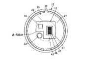
図1ないし図4において、11は電球形ランプで、この電球形ランプ11は、金属製のホルダ12、このホルダ12の一端側(電球形ランプ11のランプ軸の一端側)に取り付けられた発光モジュール13、ホルダ12の他端側に取り付けられた絶縁性を有するカバー14、このカバー14の他端側に取り付けられた口金15、発光モジュール13を覆ってホルダ12の一端側に取り付けられた透光性を有するグローブ16、およびホルダ12と口金15との間でカバー14の内側に収納された点灯回路17を備えている。 In FIG. 1 to FIG. 4,
ホルダ12は、熱伝導性が優れた例えばアルミニウムなど金属材料によって一体形成されており、中央域に胴体部21が形成され、この胴体部21の周囲にランプ軸方向に沿った複数の放熱フィン22が放射状に突出形成されている。 The
胴体部21の一端側には円柱状で中実の基体部23が形成され、他端側には他端側へ向けて開口する円筒部24が形成されている。 A cylindrical
放熱フィン22は、ホルダ12の他端側から一端側へと径方向の突出量が徐々に大きくなるように傾斜して形成されている。また、これら放熱フィン22はホルダ12の周方向に互いに略等間隔で放射状に形成され、これら放熱フィン22間に間隙25が形成されている。これら間隙25は、ホルダ12の他端側および周囲へ向けて開口され、ホルダの一端側には閉塞されている。放熱フィン22および隙間25の一端側には、基体部23の周囲にその基体部23に連続する環状の縁部26が形成されている。 The
ホルダ12の一端側の面には、中央域である基体部23の一端側の面に発光モジュール13が面接触して取り付けられる発光モジュール取付面27が形成されているとともにこの発光モジュール取付面27に発光モジュールをねじ止めする複数の取付孔28が形成され、周辺域である縁部26の一端側の面にグローブ16を取り付ける環状のグローブ取付部29が突出形成されている。このグローブ取付部29の外周には一端側であるグローブ16側が小径となる傾斜部30が形成されている。 A light emitting
ホルダ12の基体部23には、ランプ軸の中心から外れた位置にホルダ12の一端側の面と他端側である円筒部24の内面とを連通する孔部31がランプ軸方向に沿って形成され、ホルダ12の一端側の面に孔部31の一端側からホルダ12の周辺域へ向けて溝部32が形成され、これら孔部31および溝部32によって点灯回路17と発光モジュール13とを配線接続するための配線孔33が形成されている。 The
そして、ホルダ12は、ホルダ12の一端側の面から見て、基体部23の容積が放熱フィンの部分の容積より大きく、つまり、基体部23で熱を吸熱可能とする熱容量が放熱フィン22の部分の熱容量より大きい関係を有している。 The
また、発光モジュール13は、例えば、アルミニウムなどの金属材料、あるいはセラミックスやエポキシ樹脂などの絶縁材料で形成された四角形状の基板41を有し、この基板41の一端側の面である実装面に配線パターン42が形成されていとともに、実装面の中央域に複数の半導体発光素子としてのLEDチップ43がマトリクス状に配列されて実装されている。 The
複数のLEDチップ43の両側域に配置された配線パターン42の一対の電極パッド44間の方向に沿って複数のLEDチップ43がワイヤボンディングによって直列に接続されている。基板41の縁部であって、発光モジュール13がホルダ12に取り付けられた状態でホルダ12の溝部32に対向する基板41の縁部には、配線パターン42に電気的に接続されるコネクタ受45が配設されている。 The plurality of
LEDチップ43には、例えば、青色光を発するLEDチップが用いられる。基板41に実装された複数のLEDチップ43上には、例えばシリコーン樹脂など透明樹脂である封止樹脂が塗布形成されている。この封止樹脂には、LEDチップ43からの青色光の一部により励起されて黄色光を放射する蛍光体が混入されている。したがって、LEDチップ43および封止樹脂によって発光部46が構成され、この発光部46の表面である封止樹脂の表面が発光面47となり、この発光面47から白色系の照明光が放射される。 As the
基板41の四隅近傍には図示しない複数の挿通孔が形成され、これら挿通孔に挿通するねじ48をホルダ12の取付孔28に螺着することより、基板41の他端側の面がホルダ12の基体部23の一端側の面である発光モジュール取付面27に面接触した状態に取り付けられている。このとき、基板41の他端側の面とホルダ12の発光モジュール取付面27との間には、熱伝導性に優れたシートやグリスなどの熱伝導材が介在されている。そして、基板41をホルダ12の発光モジュール取付面27に取り付けた状態では、発光面47の中心がランプ軸の中心に対応して位置するとともに、ホルダ12の一端側に描かれる基体部23の投影領域(図2および図3に点線で示す領域)内に発光モジュール13の発光部46が位置し、言い換えれば放熱フィン22が形成されていない領域に発光モジュール13の発光部46が位置し、また、基板41の縁部から配線孔33の溝部32の端部が露出して開口されている。なお、この領域内に発光部46の90%以上、好ましくは95%以上が存在するように基板41が発光モジュール取付面27に面接触されていれば熱伝導は良好であり、所定の放熱効果も得られることを確認している。 A plurality of insertion holes (not shown) are formed in the vicinity of the four corners of the
また、カバー14は、例えばPBT樹脂などの絶縁材料により、他端側へ向けて開口する円筒状に形成されている。カバー14の他端側の外周部には、ホルダ12と口金15との間に介在して互いの間を絶縁する環状の鍔部51が形成されている。カバー14の一端側の面には、ホルダ12の配線孔33に同軸に連通する配線孔52が形成されている。 Moreover, the
また、口金15は、例えば、E17形やE26形などの一般照明電球用のソケットに接続可能なもので、カバー14に嵌合されてかしめられて固定されるシェル55、このシェル55の他端側に設けられる絶縁部56、およびこの絶縁部56の頂部に設けられるアイレット57を有している。 The base 15 can be connected to a socket for general lighting bulbs such as E17 type and E26 type, for example, a
また、グローブ16は、光拡散性を有するガラスあるいは合成樹脂などで、発光モジュール13を覆うように球面状に形成されている。グローブ16の他端側は開口され、この開口縁部にホルダ12のグローブ取付部29の内周側に嵌合されるとともに接着剤などで固定される嵌合部60が形成されている。 The
また、点灯回路17は、例えば、発光モジュール13のLEDチップ43に対して定電流を供給する回路であり、回路を構成する複数の回路素子が実装された回路基板を有し、この回路基板がカバー14内に収納されて固定されている。点灯回路17の入力側には、口金15のシェル55およびアイレット57が接続線で電気的に接続されている。点灯回路17の出力側には先端にコネクタ63を有する接続線64が接続され、このコネクタ63および接続線64がカバー14の配線孔52およびホルダ12の配線孔33を通じてホルダ12の一端側に引き出され、コネクタ63が基板41のコネクタ受45に接続されている。なお、この発光モジュール13との接続作業は、発光モジュール13をホルダ12にねじ止めする前に行われる。 The lighting circuit 17 is, for example, a circuit that supplies a constant current to the
また、図5には、電球形ランプ11を使用するダウンライトである照明器具70を示し、この照明器具70は、器具本体71を有し、この器具本体71内にソケット72および反射体73が配設されている。 FIG. 5 shows a lighting fixture 70 that is a downlight using the light bulb shaped
そうして、電球形ランプ11を照明器具70のソケット72に装着して通電すると、点灯回路17が動作し、発光モジュール13の複数のLEDチップ43に電力が供給され、複数のLEDチップ43が発光し、この光がグローブ16を通じて拡散放射される。 Then, when the light bulb shaped
発光モジュール13の複数のLEDチップ43の点灯時に発生する熱は、基板41に熱伝導されるとともにこの基板41からホルダ12の基体部23に熱伝導され、この基体部23から複数の放熱フィン22に熱伝導され、複数の放熱フィン22から空気中に効率よく放熱される。 Heat generated when the plurality of
このとき、ホルダ12は、ホルダ12の一端側の面から見て、基体部23の容積が放熱フィン22の部分の容積より大きく、つまり、基体部23で熱を吸熱可能とする熱容量が放熱フィン22の部分の熱容量より大きい関係を有している。そのため、基体部23の一端側の領域、好ましくは領域内に発光モジュール13の発光部46が位置していることにより、複数のLEDチップ43からの熱を、熱容量の大きい基体部23で効率よく継続的に吸熱できるため、ホルダ12の基体部23に効率よく熱伝導できるとともに基体部23から放熱フィン22への熱伝導も良好となるため放熱フィン22によって外部に効率よく放熱でき、LEDチップ43の温度上昇を効果的に抑制できる。 At this time, the
また、ホルダ12の基体部23の一端側と他端側とを連通する孔部31、およびホルダ12の一端側の面に孔部31の一端側からホルダ12の周辺域へ向けて形成された溝部32によって配線孔33を形成するため、発光モジュール13からホルダ12への熱伝導性を維持しながら、点灯回路17と発光モジュール13との配線接続を容易にできる。 Also, a
特に、配線孔33の孔部31が基体部23の中心から外れた位置に形成されているため、電球形ランプ11としての配光を考慮して発光モジュール13のLEDチップ43を基体部23の中心に対応する位置に配置していても、LEDチップ43からの熱が基体部23の中心に効率よく熱伝導できる。 In particular, since the
次に、図6に第2の実施の形態を示し、図6は電球形ランプのホルダおよび発光モジュールを一端側から見た正面図である。 Next, FIG. 6 shows a second embodiment, and FIG. 6 is a front view of the bulb-shaped lamp holder and the light emitting module as viewed from one end side.
ホルダ12には、基体部23の位置でかつランプ軸の中心から外れた位置に、ホルダ12の一端側と他端側とを連通する配線孔33が形成されている。 The
発光モジュール13の基板41は、略四角形で、そのうちの1つの角部が切り欠かれて逃げ部81が形成されている。 The
発光モジュール13をホルダ12に取り付ける際に、基板41の逃げ部81を配線孔33の位置に合わせ、配線孔33を開口するようにする。 When the
これにより、基板41の全面がホルダ12の基体部23に接触し、発光モジュール13からホルダ12への高い熱伝導性を維持しながら、配線孔33を通じての点灯回路17と発光モジュール13との配線接続を容易にできる。 Thereby, the entire surface of the
しかも、基板41に逃げ部81を形成することにより、発光モジュール13の発光面47の中心をランプ軸の中心に近付けることができ、均一な配光特性を得ることができる。 Moreover, by forming the relief portion 81 on the
次に、図7に第3の実施の形態を示し、図7は電球形ランプのホルダおよび発光モジュールを一端側から見た正面図である。 Next, FIG. 7 shows a third embodiment, and FIG. 7 is a front view of a light bulb shaped lamp holder and a light emitting module as viewed from one end side.
ホルダ12には、基体部23の位置でかつランプ軸の中心から外れた位置に、ホルダ12の一端側と他端側とを連通する配線孔33が形成されている。 The
発光モジュール13の基板41は、略四角形で、中央域に長孔状の逃げ部81が形成されている。 The
発光モジュール13をホルダ12に取り付ける際に、基板41の長孔状の逃げ部81を配線孔33の位置に合わせ、配線孔33を開口するようにする。 When attaching the
これにより、基板41の全面がホルダ12の基体部23に接触し、発光モジュール13からホルダ12への高い熱伝導性を維持しながら、配線孔33を通じての点灯回路17と発光モジュール13との配線接続を容易にできる。 Thereby, the entire surface of the
また、基板41には長孔状の逃げ部81の両側にLEDチップ43が分割して配置されていることにより、基板41の中央に長孔状の逃げ部81がありながら、均一な配光特性を得ることができる。 Further, the
なお、逃げ部81を長孔状としたが、略U字形の溝状に形成してもよい。 Although the escape portion 81 has a long hole shape, it may be formed in a substantially U-shaped groove shape.
また、LEDチップ43を分割して配置する場合には、基板41自体も分割してもよい。例えば、基板41を略L字形に形成し、一対の基板41を四角形枠状に組み合わせてホルダ12に固定し、一対の基板41間をワイヤボンディングやはんだ付け接続などによって電気的に接続するようにしてもよい。 Further, when the
11 電球形ランプ
12 ホルダ
13 発光モジュール
15 口金
17 点灯回路
21 胴体部
22 放熱フィン
23 基体部
24 円筒部
26 縁部
27 発光モジュール取付部としての発光モジュール取付面
31 孔部
32 溝部
33 配線孔
41 基板
43 半導体発光素子としてのLEDチップ
46 発光部
70 照明器具
71 器具本体
72 ソケット
81 逃げ部11 Bulb lamp
12 Holder
13 Light emitting module
15 base
17 Lighting circuit
21 Torso
22 Radiation fin
23 Base part
24 Cylindrical part
26 Edge
27 Light emitting module mounting surface as light emitting module mounting
31 hole
32 Groove
33 Wiring hole
41 Board
43 LED chips as semiconductor light emitting devices
46 Light emitter
70 Lighting equipment
71 Instrument body
72 socket
81 Escape
Claims (5)
Translated fromJapanese中央域に形成された胴体部、この胴体部の周囲に設けられた複数の放熱フィン、および前記胴体部の一端側の外周面に設けられ前記放熱フィンとつながる縁部を有し、前記胴体部には、一端側に発光モジュール取付部が設けられているとともに他端側に円筒部が設けられ、これら発光モジュール取付部と円筒部との間に中実の基体部が設けられており、前記基体部の熱容量が前記放熱フィン部分より大きく、前記基体部の一端側の領域内に前記発光モジュールの前記発光部が位置するように前記基体部の一端側の面である前記発光モジュール取付部に前記基板の他面側の面が熱伝導可能に接触されたホルダと;
前記ホルダの他端に設けられた口金と;
前記ホルダと前記口金との間で前記ホルダの前記円筒部内に一部が収容された点灯回路と;
を具備していることを特徴とする電球形ランプ。A light-emitting module having a light-emitting portion in which a plurality of semiconductor light-emitting elements are mounted on one surface of the substrate;
A body portion formed in a centralregion, a plurality of radiation fins provided around the body portion ofthis, and anedge provided on the outer peripheral surface of one end side connected to the radiating fins of the body portion, the body The part is provided with a light emitting module attaching part on one end side and a cylindrical part is provided on the other end side, and a solid base part is provided between the light emitting module attaching part and the cylindrical part, The light emitting module mounting portion which is a surface on one end side of the base portion so that the heat capacity of the base portion is larger than that of the heat radiating fin portion and the light emitting portion of the light emitting module is located in a region on one end side of the base portion. A holder having a surface on the other side of the substrate in contact with the substrate so as to be capable of conducting heat;
A base provided at the other end of the holder;
A lighting circuit partially accommodated in the cylindrical portion of the holder between the holder and the base;
Bulb-shaped lamp, characterized in that it comprisesa.
ことを特徴とする請求項1記載の電球形ランプ。The light emitting module attachment portion, said body portion including said cylindrical portion and said base portion, said heat radiating fins and, self-ballasted lamp of claim1, wherein said edge is characterized by being formed integrally.
前記発光モジュールの前記基板には、前記基板が前記基体部の一端側の面である前記発光モジュール取付部に接触した状態で前記配線孔を開口させる逃げ部が形成されている
ことを特徴とする請求項1または2記載の電球形ランプ。The holder is formed with a wiring hole that allows one end side and the other end side of the base portion to communicate with each other to enable wiring connection between the light emitting module and the lighting circuit,
The substrate of the light emitting module is provided with a relief portion that opens the wiring hole in a state where the substrate is in contact with the light emitting module mounting portion that is a surface on one end side of the base portion. The light bulb shaped lamp according to claim 1or 2 .
ことを特徴とする請求項1または2記載の電球形ランプ。The holder is formed with a hole portion that communicates one end side and the other end side of the base portion, and the one end side surface of the holder is directed from one end side of the hole portion toward the peripheral area of the holder.3. The light bulb shaped lamp according to claim 1, wherein a wiring hole that allows wiring connection between the light emitting module and the lighting circuit is formed by the hole and the groove.
前記器具本体の前記ソケットに装着される請求項1ないし4いずれか一記載の電球形ランプと;
を具備していることを特徴とする照明器具。An instrument body having a socket;
The light bulb shaped lamp according to any one of claims 1 to4, which is mounted on the socket of the instrument body;
The lighting fixture characterized by comprising.
Priority Applications (5)
| Application Number | Priority Date | Filing Date | Title |
|---|---|---|---|
| JP2009155922AJP5354191B2 (en) | 2009-06-30 | 2009-06-30 | Light bulb shaped lamp and lighting equipment |
| US12/825,956US20100327751A1 (en) | 2009-06-30 | 2010-06-29 | Self-ballasted lamp and lighting equipment |
| TW099121235ATW201102577A (en) | 2009-06-30 | 2010-06-29 | Bulb-shaped lamp and illumination device |
| CN201010216943XACN101936472A (en) | 2009-06-30 | 2010-06-29 | Bulb-shaped lamps and lighting fixtures |
| EP10006720AEP2270393A1 (en) | 2009-06-30 | 2010-06-29 | Self-ballasted lamp and lighting equipment |
Applications Claiming Priority (1)
| Application Number | Priority Date | Filing Date | Title |
|---|---|---|---|
| JP2009155922AJP5354191B2 (en) | 2009-06-30 | 2009-06-30 | Light bulb shaped lamp and lighting equipment |
Publications (2)
| Publication Number | Publication Date |
|---|---|
| JP2011014306A JP2011014306A (en) | 2011-01-20 |
| JP5354191B2true JP5354191B2 (en) | 2013-11-27 |
Family
ID=42735687
Family Applications (1)
| Application Number | Title | Priority Date | Filing Date |
|---|---|---|---|
| JP2009155922AExpired - Fee RelatedJP5354191B2 (en) | 2009-06-30 | 2009-06-30 | Light bulb shaped lamp and lighting equipment |
Country Status (5)
| Country | Link |
|---|---|
| US (1) | US20100327751A1 (en) |
| EP (1) | EP2270393A1 (en) |
| JP (1) | JP5354191B2 (en) |
| CN (1) | CN101936472A (en) |
| TW (1) | TW201102577A (en) |
Families Citing this family (18)
| Publication number | Priority date | Publication date | Assignee | Title |
|---|---|---|---|---|
| US7758223B2 (en) | 2005-04-08 | 2010-07-20 | Toshiba Lighting & Technology Corporation | Lamp having outer shell to radiate heat of light source |
| CN103470983A (en) | 2008-06-27 | 2013-12-25 | 东芝照明技术株式会社 | Light-emitting element lamp and lighting equipment |
| JP5333758B2 (en) | 2009-02-27 | 2013-11-06 | 東芝ライテック株式会社 | Lighting device and lighting fixture |
| JP5601512B2 (en) | 2009-09-14 | 2014-10-08 | 東芝ライテック株式会社 | Light emitting device and lighting device |
| JP2011091033A (en) | 2009-09-25 | 2011-05-06 | Toshiba Lighting & Technology Corp | Light-emitting module, bulb-shaped lamp and lighting equipment |
| US8324789B2 (en) | 2009-09-25 | 2012-12-04 | Toshiba Lighting & Technology Corporation | Self-ballasted lamp and lighting equipment |
| US8678618B2 (en) | 2009-09-25 | 2014-03-25 | Toshiba Lighting & Technology Corporation | Self-ballasted lamp having a light-transmissive member in contact with light emitting elements and lighting equipment incorporating the same |
| CN102032481B (en) | 2009-09-25 | 2014-01-08 | 东芝照明技术株式会社 | Lighting lamps and lighting fixtures with sockets |
| JP5475732B2 (en)* | 2011-02-21 | 2014-04-16 | 株式会社東芝 | Lighting device |
| TWM441089U (en)* | 2011-04-11 | 2012-11-11 | Molex Inc | LED Lamp |
| CN102818134B (en)* | 2011-06-10 | 2015-02-18 | 富瑞精密组件(昆山)有限公司 | Lamp |
| JP5720468B2 (en)* | 2011-07-26 | 2015-05-20 | 東芝ライテック株式会社 | Light bulb shaped LED lamp |
| US9239159B2 (en) | 2011-12-16 | 2016-01-19 | Samsung Electronics Co., Ltd. | Heat-dissipating structure for lighting apparatus and lighting apparatus |
| US8760058B2 (en) | 2012-02-02 | 2014-06-24 | Posco Led Company Ltd. | Heat sink and LED illuminating apparatus comprising the same |
| TWI580922B (en)* | 2012-03-03 | 2017-05-01 | chong-xian Huang | One-time forming of the heat pipe seat |
| KR101412959B1 (en)* | 2013-07-05 | 2014-06-27 | 주식회사 포스코엘이디 | LED lighting device |
| JP6286791B2 (en)* | 2013-12-10 | 2018-03-07 | パナソニックIpマネジメント株式会社 | Light source unit and lighting apparatus using the same |
| US11168879B2 (en)* | 2020-02-28 | 2021-11-09 | Omachron Intellectual Property Inc. | Light source |
Family Cites Families (110)
| Publication number | Priority date | Publication date | Assignee | Title |
|---|---|---|---|---|
| US1972790A (en)* | 1932-07-15 | 1934-09-04 | Crouse Hinds Co | Electric hand lamp |
| US4503360A (en)* | 1982-07-26 | 1985-03-05 | North American Philips Lighting Corporation | Compact fluorescent lamp unit having segregated air-cooling means |
| US4939420A (en)* | 1987-04-06 | 1990-07-03 | Lim Kenneth S | Fluorescent reflector lamp assembly |
| DE4235289C2 (en)* | 1992-10-20 | 1996-08-01 | Teves Gmbh Alfred | Signal light for a vehicle |
| US5323271A (en)* | 1992-11-24 | 1994-06-21 | Equestrian Co., Ltd. | Water- and air-cooled reflection mirror |
| JP2662488B2 (en)* | 1992-12-04 | 1997-10-15 | 株式会社小糸製作所 | Seal structure between front lens leg and seal groove in automotive lighting |
| US5327332A (en)* | 1993-04-29 | 1994-07-05 | Hafemeister Beverly J | Decorative light socket extension |
| JP2828584B2 (en)* | 1993-12-27 | 1998-11-25 | 株式会社小糸製作所 | Automotive headlamp |
| US5632551A (en)* | 1994-07-18 | 1997-05-27 | Grote Industries, Inc. | LED vehicle lamp assembly |
| US5537301A (en)* | 1994-09-01 | 1996-07-16 | Pacific Scientific Company | Fluorescent lamp heat-dissipating apparatus |
| US6465743B1 (en)* | 1994-12-05 | 2002-10-15 | Motorola, Inc. | Multi-strand substrate for ball-grid array assemblies and method |
| CA2225734C (en)* | 1995-06-29 | 2006-11-14 | Lynn Wiese | Localized illumination using tir technology |
| US6111359A (en)* | 1996-05-09 | 2000-08-29 | Philips Electronics North America Corporation | Integrated HID reflector lamp with HID arc tube in a pressed glass reflector retained in a shell housing a ballast |
| US5785418A (en)* | 1996-06-27 | 1998-07-28 | Hochstein; Peter A. | Thermally protected LED array |
| JPH1125919A (en)* | 1997-07-04 | 1999-01-29 | Moriyama Sangyo Kk | Electric bulb device and lighting system |
| US5947588A (en)* | 1997-10-06 | 1999-09-07 | Grand General Accessories Manufacturing Inc. | Light fixture with an LED light bulb having a conventional connection post |
| US6502968B1 (en)* | 1998-12-22 | 2003-01-07 | Mannesmann Vdo Ag | Printed circuit board having a light source |
| US6186646B1 (en)* | 1999-03-24 | 2001-02-13 | Hinkley Lighting Incorporated | Lighting fixture having three sockets electrically connected and mounted to bowl and cover plate |
| JP2000294434A (en)* | 1999-04-02 | 2000-10-20 | Hanshin Electric Co Ltd | Internal combustion engine ignition coil |
| US6227679B1 (en)* | 1999-09-16 | 2001-05-08 | Mule Lighting Inc | Led light bulb |
| US6814470B2 (en)* | 2000-05-08 | 2004-11-09 | Farlight Llc | Highly efficient LED lamp |
| US6626554B2 (en)* | 2000-05-18 | 2003-09-30 | Aaron Nathan Rincover | Light apparatus |
| US7122900B2 (en)* | 2000-06-26 | 2006-10-17 | Renesas Technology Corp. | Semiconductor device and method manufacturing the same |
| JP2002075011A (en)* | 2000-08-30 | 2002-03-15 | Matsushita Electric Ind Co Ltd | Tube ball |
| KR20020091173A (en)* | 2001-02-02 | 2002-12-05 | 코닌클리즈케 필립스 일렉트로닉스 엔.브이. | Integrated light source |
| JP2002314139A (en)* | 2001-04-09 | 2002-10-25 | Toshiba Corp | Light emitting device |
| US6598996B1 (en)* | 2001-04-27 | 2003-07-29 | Pervaiz Lodhie | LED light bulb |
| CN2489462Y (en)* | 2001-06-17 | 2002-05-01 | 广东伟雄集团有限公司 | Energy-saving lamp with insert strip |
| US6866401B2 (en)* | 2001-12-21 | 2005-03-15 | General Electric Company | Zoomable spot module |
| US6682211B2 (en)* | 2001-09-28 | 2004-01-27 | Osram Sylvania Inc. | Replaceable LED lamp capsule |
| JP2003115203A (en)* | 2001-10-03 | 2003-04-18 | Matsushita Electric Ind Co Ltd | Low pressure mercury vapor discharge lamp and method of manufacturing the same |
| US6525668B1 (en)* | 2001-10-10 | 2003-02-25 | Twr Lighting, Inc. | LED array warning light system |
| EP1467414A4 (en)* | 2001-12-29 | 2007-07-11 | Hangzhou Fuyang Xinying Dianzi | A led and led lamp |
| US6685339B2 (en)* | 2002-02-14 | 2004-02-03 | Polaris Pool Systems, Inc. | Sparkle light bulb with controllable memory function |
| US6641283B1 (en)* | 2002-04-12 | 2003-11-04 | Gelcore, Llc | LED puck light with detachable base |
| US6824296B2 (en)* | 2002-07-02 | 2004-11-30 | Leviton Manufacturing Co., Inc. | Night light assembly |
| US20040012955A1 (en)* | 2002-07-17 | 2004-01-22 | Wen-Chang Hsieh | Flashlight |
| US20040023815A1 (en)* | 2002-08-01 | 2004-02-05 | Burts Boyce Donald | Lost circulation additive, lost circulation treatment fluid made therefrom, and method of minimizing lost circulation in a subterranean formation |
| US6787999B2 (en)* | 2002-10-03 | 2004-09-07 | Gelcore, Llc | LED-based modular lamp |
| US7111961B2 (en)* | 2002-11-19 | 2006-09-26 | Automatic Power, Inc. | High flux LED lighting device |
| US6964501B2 (en)* | 2002-12-24 | 2005-11-15 | Altman Stage Lighting Co., Ltd. | Peltier-cooled LED lighting assembly |
| EP1447619A1 (en)* | 2003-02-12 | 2004-08-18 | Exterieur Vert S.A. | Lighting device, in particular projector-like sealed luminaire recessed in the ground, cooled by air circulation |
| CN2637885Y (en)* | 2003-02-20 | 2004-09-01 | 高勇 | LED lamp bulb with luminous curved surface |
| JP3885032B2 (en)* | 2003-02-28 | 2007-02-21 | 松下電器産業株式会社 | Fluorescent lamp |
| AU2003902031A0 (en)* | 2003-04-29 | 2003-05-15 | Eveready Battery Company, Inc | Lighting device |
| US6921181B2 (en)* | 2003-07-07 | 2005-07-26 | Mei-Feng Yen | Flashlight with heat-dissipation device |
| US7679096B1 (en)* | 2003-08-21 | 2010-03-16 | Opto Technology, Inc. | Integrated LED heat sink |
| US7329024B2 (en)* | 2003-09-22 | 2008-02-12 | Permlight Products, Inc. | Lighting apparatus |
| US6982518B2 (en)* | 2003-10-01 | 2006-01-03 | Enertron, Inc. | Methods and apparatus for an LED light |
| US6942360B2 (en)* | 2003-10-01 | 2005-09-13 | Enertron, Inc. | Methods and apparatus for an LED light engine |
| US7144135B2 (en)* | 2003-11-26 | 2006-12-05 | Philips Lumileds Lighting Company, Llc | LED lamp heat sink |
| US7281818B2 (en)* | 2003-12-11 | 2007-10-16 | Dialight Corporation | Light reflector device for light emitting diode (LED) array |
| USD497439S1 (en)* | 2003-12-24 | 2004-10-19 | Elumina Technolgy Incorporation | Lamp with high power LED |
| US7059748B2 (en)* | 2004-05-03 | 2006-06-13 | Osram Sylvania Inc. | LED bulb |
| US7367692B2 (en)* | 2004-04-30 | 2008-05-06 | Lighting Science Group Corporation | Light bulb having surfaces for reflecting light produced by electronic light generating sources |
| TWI257991B (en)* | 2004-05-12 | 2006-07-11 | Kun-Lieh Huang | Lighting device with auxiliary heat dissipation functions |
| US7125146B2 (en)* | 2004-06-30 | 2006-10-24 | H-Tech, Inc. | Underwater LED light |
| JP2006040727A (en)* | 2004-07-27 | 2006-02-09 | Matsushita Electric Works Ltd | Light-emitting diode lighting device and illumination device |
| US20060034077A1 (en)* | 2004-08-10 | 2006-02-16 | Tsu-Kang Chang | White light bulb assembly using LED as a light source |
| DE102004042186B4 (en)* | 2004-08-31 | 2010-07-01 | Osram Opto Semiconductors Gmbh | Optoelectronic component |
| US7165866B2 (en)* | 2004-11-01 | 2007-01-23 | Chia Mao Li | Light enhanced and heat dissipating bulb |
| US7144140B2 (en)* | 2005-02-25 | 2006-12-05 | Tsung-Ting Sun | Heat dissipating apparatus for lighting utility |
| US7255460B2 (en)* | 2005-03-23 | 2007-08-14 | Nuriplan Co., Ltd. | LED illumination lamp |
| JP2006278774A (en)* | 2005-03-29 | 2006-10-12 | Hitachi Cable Ltd | Method for manufacturing double-sided wiring board, double-sided wiring board, and base board thereof |
| US7758223B2 (en)* | 2005-04-08 | 2010-07-20 | Toshiba Lighting & Technology Corporation | Lamp having outer shell to radiate heat of light source |
| CN101660740B (en)* | 2005-04-08 | 2013-03-13 | 东芝照明技术株式会社 | Lamp |
| JP4482706B2 (en)* | 2005-04-08 | 2010-06-16 | 東芝ライテック株式会社 | Light bulb lamp |
| US7226189B2 (en)* | 2005-04-15 | 2007-06-05 | Taiwan Oasis Technology Co., Ltd. | Light emitting diode illumination apparatus |
| US7744256B2 (en)* | 2006-05-22 | 2010-06-29 | Edison Price Lighting, Inc. | LED array wafer lighting fixture |
| EP2287526B1 (en)* | 2005-07-20 | 2013-09-11 | TBT Asset Management International Limited | Illumination unit with serpentine-shaped cold cathode fluorescent lamp |
| WO2007030542A2 (en)* | 2005-09-06 | 2007-03-15 | Lsi Industries, Inc. | Linear lighting system |
| JP4715422B2 (en)* | 2005-09-27 | 2011-07-06 | 日亜化学工業株式会社 | Light emitting device |
| US20070103904A1 (en)* | 2005-11-09 | 2007-05-10 | Ching-Chao Chen | Light emitting diode lamp |
| CN2893400Y (en)* | 2006-04-12 | 2007-04-25 | 深圳市红绿蓝光电科技有限公司 | LED bulb |
| US20070247840A1 (en)* | 2006-04-21 | 2007-10-25 | Ham Byung I | Compact emergency illumination unit |
| TWM309051U (en)* | 2006-06-12 | 2007-04-01 | Grand Halo Technology Co Ltd | Light-emitting device |
| JP4300223B2 (en)* | 2006-06-30 | 2009-07-22 | 株式会社 日立ディスプレイズ | LIGHTING DEVICE AND DISPLAY DEVICE USING LIGHTING DEVICE |
| JP4367457B2 (en)* | 2006-07-06 | 2009-11-18 | パナソニック電工株式会社 | Silver film, silver film manufacturing method, LED mounting substrate, and LED mounting substrate manufacturing method |
| US7396146B2 (en)* | 2006-08-09 | 2008-07-08 | Augux Co., Ltd. | Heat dissipating LED signal lamp source structure |
| TW200837308A (en)* | 2006-09-21 | 2008-09-16 | Led Lighting Fixtures Inc | Lighting assemblies, methods of installing same, and methods of replacing lights |
| US20080080187A1 (en)* | 2006-09-28 | 2008-04-03 | Purinton Richard S | Sealed LED light bulb |
| KR101513738B1 (en)* | 2006-11-14 | 2015-04-21 | 크리, 인코포레이티드 | Lighting assemblies and components for lighting assemblies |
| KR101408613B1 (en)* | 2006-11-30 | 2014-06-20 | 크리, 인코포레이티드 | Self-ballasted solid state lighting devices |
| US20110128742A9 (en)* | 2007-01-07 | 2011-06-02 | Pui Hang Yuen | High efficiency low cost safety light emitting diode illumination device |
| US7968900B2 (en)* | 2007-01-19 | 2011-06-28 | Cree, Inc. | High performance LED package |
| CN201014414Y (en)* | 2007-02-08 | 2008-01-30 | 鸿富锦精密工业(深圳)有限公司 | Computer panel conducting and shading device |
| JP5089212B2 (en)* | 2007-03-23 | 2012-12-05 | シャープ株式会社 | LIGHT EMITTING DEVICE, LED LAMP USING THE SAME, AND METHOD FOR MANUFACTURING LIGHT EMITTING DEVICE |
| CN101307887A (en)* | 2007-05-14 | 2008-11-19 | 穆学利 | LED lighting bulb |
| EP2163808B1 (en)* | 2007-05-23 | 2014-04-23 | Sharp Kabushiki Kaisha | Lighting device |
| JP4980152B2 (en)* | 2007-06-19 | 2012-07-18 | シャープ株式会社 | Lighting device |
| JP5029893B2 (en)* | 2007-07-06 | 2012-09-19 | 東芝ライテック株式会社 | Light bulb shaped LED lamp and lighting device |
| CN101883946A (en)* | 2007-08-22 | 2010-11-10 | 量子跃进研究公司 | Lighting assemblies comprising multiple light sources with play and associated height control mechanisms |
| WO2009048951A2 (en)* | 2007-10-09 | 2009-04-16 | Philips Solid-State Lighting Solutions | Methods and apparatus for controlling respective load currents of multiple series-connected loads |
| JP2011501417A (en)* | 2007-10-10 | 2011-01-06 | クリー エル イー ディー ライティング ソリューションズ インコーポレイテッド | Lighting device and manufacturing method |
| JP4124479B1 (en)* | 2007-10-16 | 2008-07-23 | 株式会社モモ・アライアンス | Lighting device |
| DE102007055133A1 (en)* | 2007-11-19 | 2009-05-20 | Osram Gesellschaft mit beschränkter Haftung | Lighting device with a heat sink |
| US20090184646A1 (en)* | 2007-12-21 | 2009-07-23 | John Devaney | Light emitting diode cap lamp |
| JP5353216B2 (en)* | 2008-01-07 | 2013-11-27 | 東芝ライテック株式会社 | LED bulb and lighting fixture |
| CN101919315A (en)* | 2008-02-18 | 2010-12-15 | 东芝照明技术株式会社 | lighting device |
| CN102175000B (en)* | 2008-07-30 | 2013-11-06 | 东芝照明技术株式会社 | Lamp and lighting equipment |
| US7919339B2 (en)* | 2008-09-08 | 2011-04-05 | Iledm Photoelectronics, Inc. | Packaging method for light emitting diode module that includes fabricating frame around substrate |
| US8143769B2 (en)* | 2008-09-08 | 2012-03-27 | Intematix Corporation | Light emitting diode (LED) lighting device |
| US8188486B2 (en)* | 2008-09-16 | 2012-05-29 | Osram Sylvania Inc. | Optical disk for lighting module |
| JP4651701B2 (en)* | 2008-10-17 | 2011-03-16 | 三洋電機株式会社 | Lighting equipment |
| US7918587B2 (en)* | 2008-11-05 | 2011-04-05 | Chaun-Choung Technology Corp. | LED fixture and mask structure thereof |
| DE202008016231U1 (en)* | 2008-12-08 | 2009-03-05 | Huang, Tsung-Hsien, Yuan Shan | Heat sink module |
| US7963686B2 (en)* | 2009-07-15 | 2011-06-21 | Wen-Sung Hu | Thermal dispersing structure for LED or SMD LED lights |
| US20110079814A1 (en)* | 2009-10-01 | 2011-04-07 | Yi-Chang Chen | Light emitted diode substrate and method for producing the same |
| US8602593B2 (en)* | 2009-10-15 | 2013-12-10 | Cree, Inc. | Lamp assemblies and methods of making the same |
| TWI396844B (en)* | 2009-12-15 | 2013-05-21 | Biosensors Electrode Technology Co Ltd | Electrode for biosensor, manufacturing method thereof and biosensor thereof |
- 2009
- 2009-06-30JPJP2009155922Apatent/JP5354191B2/ennot_activeExpired - Fee Related
- 2010
- 2010-06-29EPEP10006720Apatent/EP2270393A1/ennot_activeWithdrawn
- 2010-06-29USUS12/825,956patent/US20100327751A1/ennot_activeAbandoned
- 2010-06-29TWTW099121235Apatent/TW201102577A/enunknown
- 2010-06-29CNCN201010216943XApatent/CN101936472A/enactivePending
Also Published As
| Publication number | Publication date |
|---|---|
| JP2011014306A (en) | 2011-01-20 |
| CN101936472A (en) | 2011-01-05 |
| US20100327751A1 (en) | 2010-12-30 |
| TW201102577A (en) | 2011-01-16 |
| EP2270393A1 (en) | 2011-01-05 |
Similar Documents
| Publication | Publication Date | Title |
|---|---|---|
| JP5354191B2 (en) | Light bulb shaped lamp and lighting equipment | |
| JP5327472B2 (en) | Light bulb shaped lamp and lighting equipment | |
| CN103486464B (en) | Bulb-shaped lamp and ligthing paraphernalia | |
| JP5246402B2 (en) | Light bulb shaped lamp | |
| CN102032479B (en) | Bulb-shaped lamp and illuminator | |
| JP5360402B2 (en) | Light bulb shaped lamp and lighting equipment | |
| JP2011091033A (en) | Light-emitting module, bulb-shaped lamp and lighting equipment | |
| JP2008034140A (en) | Led lighting device | |
| WO2011087023A1 (en) | Light bulb-shaped lamp and lighting fixture | |
| CN102032480A (en) | Self-ballasted lamp and lighting equipment | |
| JP2010277910A5 (en) | ||
| JP2010073337A5 (en) | ||
| JP5575715B2 (en) | Light bulb type lighting device | |
| JP5802497B2 (en) | Light bulb type lighting device | |
| JP5382335B2 (en) | Light bulb shaped lamp and lighting equipment | |
| JP6277014B2 (en) | Light bulb type lighting device | |
| JP6803553B2 (en) | Lighting device | |
| JP2011181252A (en) | Lighting fixture | |
| JP5674065B2 (en) | Light bulb shaped lamp | |
| WO2014024339A1 (en) | Bulb-type lamp, illumination device, and method for manufacturing bulb-type lamp | |
| JP2014120412A (en) | LED lamp | |
| JP2011076880A (en) | Bulb-shaped lamp, and lighting fixture | |
| JP2014003032A (en) | Electric bulb type lamp and luminaire | |
| JP5822068B2 (en) | Lighting device | |
| JP2014146574A (en) | Lamp and lighting device |
Legal Events
| Date | Code | Title | Description |
|---|---|---|---|
| A621 | Written request for application examination | Free format text:JAPANESE INTERMEDIATE CODE: A621 Effective date:20120224 | |
| A131 | Notification of reasons for refusal | Free format text:JAPANESE INTERMEDIATE CODE: A131 Effective date:20130313 | |
| A521 | Request for written amendment filed | Free format text:JAPANESE INTERMEDIATE CODE: A523 Effective date:20130507 | |
| A131 | Notification of reasons for refusal | Free format text:JAPANESE INTERMEDIATE CODE: A131 Effective date:20130522 | |
| A521 | Request for written amendment filed | Free format text:JAPANESE INTERMEDIATE CODE: A523 Effective date:20130710 | |
| TRDD | Decision of grant or rejection written | ||
| A01 | Written decision to grant a patent or to grant a registration (utility model) | Free format text:JAPANESE INTERMEDIATE CODE: A01 Effective date:20130731 | |
| A61 | First payment of annual fees (during grant procedure) | Free format text:JAPANESE INTERMEDIATE CODE: A61 Effective date:20130813 | |
| LAPS | Cancellation because of no payment of annual fees |