JP5348521B2 - LCD panel - Google Patents
LCD panelDownload PDFInfo
- Publication number
- JP5348521B2 JP5348521B2JP2008168498AJP2008168498AJP5348521B2JP 5348521 B2JP5348521 B2JP 5348521B2JP 2008168498 AJP2008168498 AJP 2008168498AJP 2008168498 AJP2008168498 AJP 2008168498AJP 5348521 B2JP5348521 B2JP 5348521B2
- Authority
- JP
- Japan
- Prior art keywords
- liquid crystal
- display panel
- crystal display
- conductive layer
- electrode
- Prior art date
- Legal status (The legal status is an assumption and is not a legal conclusion. Google has not performed a legal analysis and makes no representation as to the accuracy of the status listed.)
- Active
Links
Images


Classifications
- G—PHYSICS
- G02—OPTICS
- G02F—OPTICAL DEVICES OR ARRANGEMENTS FOR THE CONTROL OF LIGHT BY MODIFICATION OF THE OPTICAL PROPERTIES OF THE MEDIA OF THE ELEMENTS INVOLVED THEREIN; NON-LINEAR OPTICS; FREQUENCY-CHANGING OF LIGHT; OPTICAL LOGIC ELEMENTS; OPTICAL ANALOGUE/DIGITAL CONVERTERS
- G02F1/00—Devices or arrangements for the control of the intensity, colour, phase, polarisation or direction of light arriving from an independent light source, e.g. switching, gating or modulating; Non-linear optics
- G02F1/01—Devices or arrangements for the control of the intensity, colour, phase, polarisation or direction of light arriving from an independent light source, e.g. switching, gating or modulating; Non-linear optics for the control of the intensity, phase, polarisation or colour
- G02F1/13—Devices or arrangements for the control of the intensity, colour, phase, polarisation or direction of light arriving from an independent light source, e.g. switching, gating or modulating; Non-linear optics for the control of the intensity, phase, polarisation or colour based on liquid crystals, e.g. single liquid crystal display cells
- G02F1/133—Constructional arrangements; Operation of liquid crystal cells; Circuit arrangements
- G02F1/1333—Constructional arrangements; Manufacturing methods
- G02F1/1345—Conductors connecting electrodes to cell terminals
- G—PHYSICS
- G02—OPTICS
- G02F—OPTICAL DEVICES OR ARRANGEMENTS FOR THE CONTROL OF LIGHT BY MODIFICATION OF THE OPTICAL PROPERTIES OF THE MEDIA OF THE ELEMENTS INVOLVED THEREIN; NON-LINEAR OPTICS; FREQUENCY-CHANGING OF LIGHT; OPTICAL LOGIC ELEMENTS; OPTICAL ANALOGUE/DIGITAL CONVERTERS
- G02F1/00—Devices or arrangements for the control of the intensity, colour, phase, polarisation or direction of light arriving from an independent light source, e.g. switching, gating or modulating; Non-linear optics
- G02F1/01—Devices or arrangements for the control of the intensity, colour, phase, polarisation or direction of light arriving from an independent light source, e.g. switching, gating or modulating; Non-linear optics for the control of the intensity, phase, polarisation or colour
- G02F1/13—Devices or arrangements for the control of the intensity, colour, phase, polarisation or direction of light arriving from an independent light source, e.g. switching, gating or modulating; Non-linear optics for the control of the intensity, phase, polarisation or colour based on liquid crystals, e.g. single liquid crystal display cells
- G02F1/133—Constructional arrangements; Operation of liquid crystal cells; Circuit arrangements
- G02F1/1333—Constructional arrangements; Manufacturing methods
- G02F1/1343—Electrodes
- G02F1/13439—Electrodes characterised by their electrical, optical, physical properties; materials therefor; method of making
- G—PHYSICS
- G02—OPTICS
- G02F—OPTICAL DEVICES OR ARRANGEMENTS FOR THE CONTROL OF LIGHT BY MODIFICATION OF THE OPTICAL PROPERTIES OF THE MEDIA OF THE ELEMENTS INVOLVED THEREIN; NON-LINEAR OPTICS; FREQUENCY-CHANGING OF LIGHT; OPTICAL LOGIC ELEMENTS; OPTICAL ANALOGUE/DIGITAL CONVERTERS
- G02F1/00—Devices or arrangements for the control of the intensity, colour, phase, polarisation or direction of light arriving from an independent light source, e.g. switching, gating or modulating; Non-linear optics
- G02F1/01—Devices or arrangements for the control of the intensity, colour, phase, polarisation or direction of light arriving from an independent light source, e.g. switching, gating or modulating; Non-linear optics for the control of the intensity, phase, polarisation or colour
- G02F1/13—Devices or arrangements for the control of the intensity, colour, phase, polarisation or direction of light arriving from an independent light source, e.g. switching, gating or modulating; Non-linear optics for the control of the intensity, phase, polarisation or colour based on liquid crystals, e.g. single liquid crystal display cells
- G02F1/133—Constructional arrangements; Operation of liquid crystal cells; Circuit arrangements
- G02F1/1333—Constructional arrangements; Manufacturing methods
- G02F1/1343—Electrodes
- G02F1/134309—Electrodes characterised by their geometrical arrangement
- G02F1/134372—Electrodes characterised by their geometrical arrangement for fringe field switching [FFS] where the common electrode is not patterned
Landscapes
- Physics & Mathematics (AREA)
- Nonlinear Science (AREA)
- Mathematical Physics (AREA)
- Chemical & Material Sciences (AREA)
- Crystallography & Structural Chemistry (AREA)
- General Physics & Mathematics (AREA)
- Optics & Photonics (AREA)
- Liquid Crystal (AREA)
Description
Translated fromJapanese本発明は、横電界方式の液晶表示パネルに関し、特にスリット状開口を有する上電極が共通電極として作動する横電界方式の液晶表示パネルに関するものである。 The present invention relates to a horizontal electric field type liquid crystal display panel, and more particularly to a horizontal electric field type liquid crystal display panel in which an upper electrode having a slit-like opening operates as a common electrode.
液晶表示パネルはCRT(陰極線管)と比較して軽量、薄型、低消費電力という特徴があるため、表示用として多くの電子機器に使用されている。液晶表示パネルは、配向膜に対してラビング処理することにより所定方向に整列した液晶分子の向きを電界により変えて、光の透過量ないし反射量を変化させて画像を表示させるものである。 Liquid crystal display panels are characterized by their light weight, thinness, and low power consumption compared to CRTs (cathode ray tubes), and are therefore used in many electronic devices for display purposes. The liquid crystal display panel displays an image by changing the direction of liquid crystal molecules aligned in a predetermined direction by an electric field by rubbing the alignment film, thereby changing the amount of light transmitted or reflected.
液晶表示パネルの液晶層に電界を印加する方法として、縦電界方式のものと横電界方式のものとがある。縦電界方式の液晶表示パネルは、液晶層を挟んで配置される一対の電極により、概ね縦方向の電界を液晶分子に印加するものである。この縦電界方式の液晶表示パネルとしては、TN(Twisted Nematic)モード、VA(Vertical Alignment)モード、MVA(Multi-domain Vertical Alignment)モード等のものが知られている。横電界方式の液晶表示パネルは、液晶層を挟んで配設される一対の基板のうちの一方の内面側に一対の電極を互いに絶縁して設け、概ね横方向の電界を液晶分子に対して印加するものである。この横電界方式の液晶表示パネルとしては、一対の電極が平面視で重ならないIPS(In-Plane Switching)モードのものと、重なるFFS(Fringe Field Switching)モードのものとが知られている。 As a method of applying an electric field to a liquid crystal layer of a liquid crystal display panel, there are a vertical electric field type and a horizontal electric field type. A vertical electric field type liquid crystal display panel applies a substantially vertical electric field to liquid crystal molecules by a pair of electrodes arranged with a liquid crystal layer interposed therebetween. Known examples of the vertical electric field type liquid crystal display panel include a TN (Twisted Nematic) mode, a VA (Vertical Alignment) mode, and an MVA (Multi-domain Vertical Alignment) mode. A horizontal electric field type liquid crystal display panel is provided with a pair of electrodes insulated from each other on one inner surface side of a pair of substrates disposed with a liquid crystal layer interposed therebetween, and a substantially horizontal electric field is applied to liquid crystal molecules. To be applied. As this lateral electric field type liquid crystal display panel, there are known an IPS (In-Plane Switching) mode in which a pair of electrodes do not overlap in a plan view and an FFS (Fringe Field Switching) mode in which they overlap.
このうち、FFSモードの液晶表示パネルは、絶縁膜を介して共通電極と画素電極とからなる一対の電極をそれぞれ異なる層に配置し、液晶層側の共通電極又は画素電極にスリット状の開口を設け、このスリット状開口を通る概ね横方向の電界を液晶層に印加するものである。このFFSモードの液晶表示パネルは、広い視野角を得ることができると共に画像コントラストを改善できるという効果があるので、近年、多く用いられるようになってきている。このFFSモードの液晶表示パネルには、画素電極がスイッチング素子としてのTFT(Thin Film Transistor)と同じ平面に形成されたもの(下記特許文献1参照)と、共通電極及び画素電極が共にTFTの上方に配置されたもの(下記特許文献2参照)とが知られている。 Among these, in the FFS mode liquid crystal display panel, a pair of electrodes including a common electrode and a pixel electrode are arranged in different layers with an insulating film interposed therebetween, and slit-like openings are formed in the common electrode or the pixel electrode on the liquid crystal layer side. And a substantially horizontal electric field passing through the slit-shaped opening is applied to the liquid crystal layer. The FFS mode liquid crystal display panel is widely used in recent years because it can obtain a wide viewing angle and improve image contrast. In this FFS mode liquid crystal display panel, a pixel electrode is formed on the same plane as a TFT (Thin Film Transistor) as a switching element (see Patent Document 1 below), and a common electrode and a pixel electrode are both above the TFT. (Refer to the following Patent Document 2).
このうち、共通電極及び画素電極が共にTFTの上方に配置された液晶表示パネルは、TFT等の表面が樹脂層から形成される層間膜で被覆され、この層間膜の表面に透明導電性材料からなる下電極が形成されている。この下電極は画素電極及び共通電極の何れとしても作動させることが可能である。この下電極を画素電極として作動させる場合、層間膜にコンタクトホールが形成され、画素電極はコンタクトホールを介してスイッチング素子と電気的に接続されている。そして、下電極の表面には絶縁膜を介して画素毎に複数のスリット状開口が形成された透明導電性材料からなる上電極が複数の画素に跨ってベタ状に形成されている。この上電極は、表示領域の周囲に形成されたコモン配線に電気的に接続され、共通電極として作動する。このような上電極及び下電極が共にTFTの上方に配置された液晶表示パネルのうち、下電極が画素電極として作動すると共に上電極が共通電極として作動するFFSモードの液晶表示パネルは、TFTや画素間の境界近傍での開口が広くなり、また、表示領域内に共通電極の配線がないために開口率が高くなるという利点を有している。
しかしながら、上述のような従来のFFSモードの液晶表示パネルは、スリット状開口を有する共通電極が複数の画素にまたがって形成されると、共通電極の外部への電気的接続は表示領域の周縁部で行われるために、共通電極の抵抗値が大きくなり、フリッカやクロストークの不良をもたらすという問題があった。一方、IPSモードの液晶表示パネルにおいては、たとえば上記特許文献3に開示されているように、画素電極及び共通電極共に透明導電性材料で形成した際の各電極の電気抵抗が大きくなることを防止する目的で、画素電極及び共通電極共に透明電極と金属電極との二重構造とすることが知られている。しかしながら、FFSモードの液晶表示パネルの場合、画素電極と共通電極とが平面視で重畳していることから、画素電極及び共通電極共に透明電極と金属電極との二重構造とすることは開口率の低下に繋がるため、採用することができない。 However, in the conventional FFS mode liquid crystal display panel as described above, when the common electrode having the slit-like opening is formed across a plurality of pixels, the electrical connection to the outside of the common electrode is performed at the periphery of the display region. Therefore, there is a problem that the resistance value of the common electrode is increased and flicker and crosstalk are defective. On the other hand, in an IPS mode liquid crystal display panel, for example, as disclosed in Patent Document 3, the electrical resistance of each electrode when the pixel electrode and the common electrode are formed of a transparent conductive material is prevented. For this purpose, it is known that both the pixel electrode and the common electrode have a double structure of a transparent electrode and a metal electrode. However, in the case of the FFS mode liquid crystal display panel, since the pixel electrode and the common electrode overlap each other in a plan view, it is important that the pixel electrode and the common electrode have a double structure of a transparent electrode and a metal electrode. Can not be adopted because it leads to a decrease in
本発明は上記問題点を解決すべくなされたものであって、本発明の目的は共通電極の電気抵抗値を小さくすることによりフリッカやクロストークを低減したFFSモードの液晶表示パネルを提供することにある。 The present invention has been made to solve the above problems, and an object of the present invention is to provide an FFS mode liquid crystal display panel in which flicker and crosstalk are reduced by reducing the electric resistance value of the common electrode. It is in.
上記目的を達成するため、本発明の液晶表示パネルは、液晶層を挟持して対向配置された一対の基板を有し、一対の基板のうちの一方には、表示領域にマトリクス状に配置された複数の走査線及び信号線と、表示領域の周縁部に沿って形成された共通配線と、少なくとも表示領域の全体に亘って形成された層間膜と、層間膜の表面に複数の走査線及び信号線で区画された画素領域毎に形成された透明導電性材料からなる画素電極と、表示領域の画素電極上及び層間膜上に形成された電極間絶縁膜と、電極間絶縁膜上の全面に形成され、画素領域毎に複数のスリットが形成されていると共に共通配線と電気的に接続された透明導電性材料からなる共通電極と、を備えた液晶表示パネルである。共通電極の表面又は共通電極と電極間絶縁膜との間であって、平面視で走査線及び信号線と重畳する位置に、共通電極を構成する透明導電性材料よりも導電性が良好な導電性層を有し、共通電極は、表示領域を覆うように表示領域の周縁部まで延在され、第1のコンタクトホールを介して共通配線と電気的に接続され、導電性層は、表示領域の周縁部まで延在され、第2のコンタクトホールを介して共通配線と電気的に接続される。To achieve the above object, a liquid crystal display panel of the present invention includes a pair of substrates facing each other with the liquid crystal layer issandwiched on one of the substrates ofa pair are arranged in a matrix in the display region a plurality of scanning lines and signallines, a common wiring formed along the periphery of thetable display region, and the interlayer film formed over the entire at least the displayarea,several on the surface ofthe layer between the film of a pixel electrode made of a transparent conductive material formed on each section pixel area in the scanning lines and signallines, and the inter-electrode insulating film formed onthe table display region on the pixel electrode and the interlayerfilm, electrodes It is formed on the entire surface of the interphase insulatingfilm, liquid crystal and a common electrode consisting ofcommon wiring and electrically connected to the transparent conductivematerial co the plurality of slits are formed in eachpicture element region It is a display panel. Surface of the common electrodeora betweencommon electrodeand the conductive interelectrode insulating film, in a position overlapping with査線and signal linesrun in a planview, conductivity than the transparent conductive material constituting the common electrode Has a good conductive layer, the common electrode extends to the peripheral edge of the display region so as to cover the display region, and is electrically connected to the common wiring through the first contact hole. Is extended to the peripheral edge of the display region and is electrically connected to the common wiring through the second contact hole .
本発明の液晶表示パネルは、層間膜の表面に複数の走査線及び信号線で区画された画素領域毎に形成された透明導電性材料からなる画素電極と、表示領域の画素電極上及び層間膜上に形成された電極間絶縁膜と、電極間絶縁膜上の全面に形成され、画素領域毎に複数のスリットが形成されていると共に共通配線と電気的に接続された透明導電性材料からなる共通電極を備えている。係る構成によって本発明の液晶表示パネルはFFSモードで作動するものとなる。なお、絶縁膜としては酸化ケイ素ないし窒化ケイ素等の無機絶縁膜を使用し得る。また、層間膜としては、透明性が良好で、電気絶縁性に優れた感光性又は非感光性の樹脂材料を適宜選択して使用し得る。更に、画素電極及び共通電極としてはITO(Indium Tin Oxide)ないしIZO(Indium Zinc Oxide)等の透明導電性材料が使用される。The liquid crystal display panel of the present invention includes a pixel electrode made of a transparent conductive material formed on each section pixel area bymultiple scanning lines and signal lineson the surface of the interlayerfilm, the pixel electrode of thetable display region and inter-electrode insulating film formed on the interlayerfilm, is formed on the entire surface of theconductive interelectrode insulating filmisCommon wiring electrically connectedto the co the plurality of slits in eachpicture element region is formed And a common electrode made of a transparent conductive material. With this configuration, the liquid crystal display panel of the present invention operates in the FFS mode. As the insulating film, an inorganic insulating film such as silicon oxide or silicon nitride can be used. Further, as the interlayer film, a photosensitive or non-photosensitive resin material having good transparency and excellent electrical insulation can be appropriately selected and used. Further, a transparent conductive material such as ITO (Indium Tin Oxide) or IZO (Indium Zinc Oxide) is used as the pixel electrode and the common electrode.
更に、本発明の液晶表示パネルにおいては、共通電極の表面又は共通電極と電極間絶縁膜との間であって、平面視で走査線及び信号線と重畳する位置に、共通電極を構成する透明導電性材料よりも導電性が良好な導電性層が形成されている。FFSモードの液晶表示パネルにおいて、スリット状開口を有する共通電極が複数の画素にまたがって形成されると、その外部への配線は表示領域の周縁部で行われるために、共通電極の抵抗値が大きくなる。共通電極の抵抗値が大きくなると、共通電極の電位が変動するため、フリッカやクロストークの原因となる。しかしながら、共通電極の表面又は共通電極と電極間絶縁膜との間に、平面視で走査線及び信号線と重畳する位置に共通電極を構成する透明導電性材料よりも導電性が良好な導電性層が形成されていると、見かけ上共通電極の電気抵抗が小さくなる。そのため、本発明の液晶表示パネルによれば、フリッカやクロストークが抑制された表示画質が良好な液晶表示パネルが得られる。Further, in the liquid crystal display panel of the presentinvention,also the surface of thecommon electrodebe betweencommon electrode and the inter-electrode insulating film, in a position overlapping with査線and signal linesrun in a planview, the common electrode A conductive layer having better conductivity than that of the transparent conductive material constituting the film is formed. In an FFS mode liquid crystal display panel, when a common electrode having a slit-like opening is formed across a plurality of pixels, the wiring to the outside is performed at the periphery of the display region. growing. When the resistance value of the common electrode increases, the potential of the common electrode changes, which causes flicker and crosstalk. However,also the surface of the common electrode between thecommon electrode and the inter-electrode insulating film, conductive than the transparent conductive material constituting theCommon electrodeat a position overlapping with査線and signal linesrun in a plan view If a good conductive layer is formed, the electrical resistance of the common electrode is apparently reduced. Therefore, according to the liquid crystal display panel of the present invention, it is possible to obtain a liquid crystal display panel with good display image quality in which flicker and crosstalk are suppressed.
なお、共通電極を構成する透明導電性材料よりも導電性が良好な導電性層は、平面視で走査線及び信号線と重畳する位置に形成されるので、液晶表示パネルの明るさに影響を与えることがない。そのため、共通電極を構成する透明導電性材料よりも導電性が良好な導電性層は、透明であっても不透明であってもよく、金属薄膜、金属フィラーを樹脂に混合分散させた導電性樹脂材料からなる薄膜、導電性炭素薄膜等を使用することができる。
共通配線は、通常金属材料である走査線形成材料又は信号線形成材料と同一の材料で形成される。また、透明導電性材料と金属材料との間の接触抵抗は、金属材料と金属材料との間の接触抵抗よりも大きい。そのため、係る態様の液晶表示パネルによれば、導電性層と共通配線との間の接触抵抗をより小さくすることができるので、よりフリッカやクロストークが少なく、表示画質が良好な液晶表示パネルが得られる。The conductive good conductivity layer than the transparent conductive material constituting the common electrode, since it is formed at a position overlapping with査線and signal linesrun in a plan view, affect the brightness of the liquid crystal display panel Never give. Therefore, the conductive layer having better conductivity than the transparent conductive material constituting the common electrode may be transparent or opaque, and a conductive resin in which a metal thin film and a metal filler are mixed and dispersed in a resin. A thin film made of a material, a conductive carbon thin film or the like can be used.
The common wiring is formed of the same material as the scanning line forming material or the signal line forming material, which is usually a metal material. Further, the contact resistance between the transparent conductive material and the metal material is larger than the contact resistance between the metal material and the metal material. Therefore, according to the liquid crystal display panel of this aspect, since the contact resistance between the conductive layer and the common wiring can be further reduced, there is a liquid crystal display panel with less flicker and crosstalk and good display image quality. can get.
また、本発明に係る液晶表示パネルにおいては、導電性層は遮光性であることが好ましい。In the liquid crystal display panel accordingto the present invention, the conductive layer is preferably light-shielding.
液晶表示パネルにおいては、走査線及び信号線の近傍からの光漏れ防止及びコントラストの向上の目的で、特に平面視で走査線及び信号線と重畳する位置のカラーフィルタ基板側にブラックマトリクスが形成されている。そのため、係る態様の液晶表示パネルによれば、遮光性の導電性層が平面視で走査線及び信号線と重畳する位置に形成されているので、特にカラーフィルタ層にブラックマトリクスを形成しなくても光漏れ防止の機能を奏させることができるようになる。 In a liquid crystal display panel, a black matrix is formed on the side of the color filter substrate, particularly at a position overlapping the scanning lines and signal lines in plan view, for the purpose of preventing light leakage from the vicinity of the scanning lines and signal lines and improving the contrast. ing. Therefore, according to the liquid crystal display panel of this aspect, since the light-shielding conductive layer is formed at a position overlapping the scanning line and the signal line in plan view, a black matrix is not particularly formed in the color filter layer. The light leakage prevention function can be achieved.
また、本発明に係る液晶表示パネルにおいては、導電性層は金属材料からなることが好ましい。In the liquid crystal display panel accordingto the present invention, the conductive layer is preferably made of a metal material.
金属材料は、透明導電性材料に比すると、導電性が極めて良好であると共に遮光性である。従って、係る態様の液晶表示パネルによれば、金属材料からなる導電性層の厚さが薄くても見かけ上共通電極の電気抵抗を小さくすることができる上、金属材料の厚さが液晶の配向特性に影響を与え難くなるので、表示画質が良好な液晶表示パネルが得られる。なお、係る態様の液晶表示パネルにおいて使用し得る金属材料としては、アルミニウム、アルミニウム合金、モリブデン、タングステン、チタン、銅等を使用することができ、また、1層構造であっても複層構造であってもよい。 The metal material has extremely good conductivity and light shielding properties as compared with the transparent conductive material. Therefore, according to the liquid crystal display panel of such an embodiment, the electrical resistance of the common electrode can be apparently reduced even when the conductive layer made of the metal material is thin, and the thickness of the metal material is the orientation of the liquid crystal. Since it is difficult to affect the characteristics, a liquid crystal display panel with good display image quality can be obtained. In addition, as a metal material that can be used in the liquid crystal display panel of such an embodiment, aluminum, aluminum alloy, molybdenum, tungsten, titanium, copper, or the like can be used, and even a single layer structure has a multilayer structure. There may be.
また、本発明に係る液晶表示パネルにおいては、導電性層の幅は走査線及び信号線の幅と同じか或いは細いことが好ましい。In the liquid crystal display panelaccording to the presentinvention, the width of theconductive layeris equal to or thinner it is preferable the width of therun査線and signal lines.
係る態様の液晶表示パネルによれば、導電性層の幅を走査線及び信号線の幅と同じか或いは細くしたので、開口度の低下が小さくなり、明るい表示の液晶表示パネルが得られる。特に導電性層の幅を走査線及び信号線の幅よりも細くすると、製造時のマスクずれ等によって導電性層が走査線や信号線からはみ出して開口率が低下することを防止することができるようになる。According to embodiments the liquid crystal display panel according, since the same or have thin and width ofthe run査線and signal lines of the conductive layer, decrease in aperture ratio is reduced, resulting a bright display liquid crystal display panel. With particular narrower than the width of the査線and signal linesrun the width of the conductive layer, is the aperture ratio conductive layer by mask misalignment or the like during manufacturing protrudes from the scanning lines and signal lines can be prevented from being lowered become able to.
また、本発明に係る液晶表示パネルにおいては、導電性層の幅は走査線及び信号線の幅よりも太くすることができる。Further, in the liquid crystal display panelaccording to the presentinvention, the width of theconductive layermay be thicker than the width of therun査線and signal lines.
係る態様の液晶表示パネルによれば、走査線及び信号線の近傍からの光漏れをより少なくすることができるので、導電性層をブラックマトリクスとして使用できると共に、よりコントラストが良好な液晶表示パネルが得られる。According to the liquid crystal display panel of this aspect, light leakage from the vicinity of the scanning lines and the signal lines can be reduced, sothat the conductive layer can be used as a black matrix and the contrast is better. Is obtained.
以下、図面を参照して本発明の最良の実施形態を説明する。但し、以下に示す実施形態は、本発明の技術思想を具体化するための液晶表示パネルの一例を示すものであって、本発明をこの液晶表示パネルに特定することを意図するものではなく、特許請求の範囲に含まれるその他の実施形態のものにも等しく適応し得るものである。なお、この明細書における説明のために用いられた各図面においては、各層や各部材を図面上で認識可能な程度の大きさとするため、各層や各部材毎に縮尺を異ならせて表示しており、必ずしも実際の寸法に比例して表示されているものではない。 Hereinafter, the best embodiment of the present invention will be described with reference to the drawings. However, the embodiment shown below shows an example of a liquid crystal display panel for embodying the technical idea of the present invention, and is not intended to specify the present invention for this liquid crystal display panel. Other embodiments that fall within the scope of the claims are equally applicable. In each drawing used for the description in this specification, each layer and each member are displayed in different scales so that each layer and each member can be recognized on the drawing. However, it is not necessarily displayed in proportion to the actual dimensions.
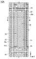
図1は第1実施形態の液晶表示パネルのカラーフィルタ基板を透視して表した1画素分の平面図である。図2は図1のII−II線に沿った断面図である。図3は図1のIII−III線に沿った断面図である。図4は第1実施形態の液晶表示パネルの共通電極における金属配線部分の一部を示す平面図である。図5は第2実施形態の液晶表示パネルのカラーフィルタ基板を透視して表した1画素分の平面図である。図6は図5のVI−VI線に沿った断面図である。図7は図5のVII−VII線に沿った断面図である。 FIG. 1 is a plan view of one pixel, which is seen through the color filter substrate of the liquid crystal display panel of the first embodiment. FIG. 2 is a sectional view taken along line II-II in FIG. FIG. 3 is a sectional view taken along line III-III in FIG. FIG. 4 is a plan view showing a part of the metal wiring portion in the common electrode of the liquid crystal display panel of the first embodiment. FIG. 5 is a plan view for one pixel, which is seen through the color filter substrate of the liquid crystal display panel of the second embodiment. 6 is a cross-sectional view taken along line VI-VI in FIG. FIG. 7 is a cross-sectional view taken along line VII-VII in FIG.
[第1実施形態]
第1実施形態に係る液晶表示パネル10Aを図1〜図4を用いて説明する。第1実施形態に係る液晶表示パネル10Aは、液晶層11をアレイ基板12及びカラーフィルタ基板13との間に挟持している。液晶層11の厚みは図示しない柱状スペーサによって均一に維持される。アレイ基板12の背面及びカラーフィルタ基板13の前面にはそれぞれ偏光板(いずれも図示省略)が貼付されており、また、アレイ基板12の背面側には光を照射するバックライト(図示省略)が配設されている。[First Embodiment]
A liquid
まず、アレイ基板12の構成について説明する。アレイ基板12は、ガラスや石英、プラスチック等からなる第1基板本体18の液晶層11側に、複数の走査線19が平行に形成されており、走査線19を覆ってゲート絶縁膜20が形成されている。この走査線19は、アルミニウム金属、アルミニウム合金、モリブデン等の不透明な金属で形成され、図1におけるX軸方向に延在している。また、ゲート絶縁膜20は酸化ケイ素ないし窒化ケイ素等の無機絶縁膜から形成されている。 First, the configuration of the
ゲート絶縁膜20上に、例えば、アモルファスシリコンからなる半導体層21が形成されており、半導体層21に一部乗り上げるようにしてソース電極Sと、ドレイン電極Dとが形成されている。半導体層21はゲート絶縁膜20を介して走査線19から分岐した部分と対向配置されており、この走査線19から分岐した部分がTFTのゲート電極Gを構成している。ソース電極Sは信号線22から分岐した部分からなる。信号線22及びドレイン電極Dは、それぞれアルミニウム金属、アルミニウム合金、モリブデン等の不透明な金属で形成され、信号線22は図1のY軸方向に延在している。 A
半導体層21、ソース電極S、ドレイン電極Dを覆って、酸化ケイ素ないし窒化ケイ素等の無機絶縁膜からなるパッシベーション膜23が形成され、そのパッシベーション膜23を覆って樹脂材料からなる層間膜24が形成されている。層間膜24としては、透明性が良好で、電気絶縁性に優れた感光性又は非感光性の樹脂材料を適宜選択して使用し得る。層間膜24を覆うように、ITO、IZO等の透明導電材料からなる画素電極25が形成されている。パッシベーション膜23及び層間膜24を貫通してドレイン電極Dに達するように第1コンタクトホール26が形成されており、この第1コンタクトホール26を介して画素電極25とドレイン電極Dとが電気的に接続されている。 A
画素電極25を覆って酸化ケイ素ないし窒化ケイ素等の無機絶縁膜からなる電極間絶縁膜27が形成されている。この電極間絶縁膜27は、画素電極25及び層間膜24の表面が荒れないようにするため、パッシベーション膜23よりも低温成膜条件で形成される。また、画素電極25及びこの電極間絶縁膜27の液晶層11側の表面には、ITOないしIZOからなる透明導電材料からなる共通電極28が形成されている。この共通電極28は、表示領域38の周辺部で第2コンタクトホール41を介して共通配線40(図4参照)と電気的に接続されている。また、共通電極28の液晶層11側には、透明導電性材料からなる共通電極28よりも導電性が良好な材料からなる導電性層29aが、平面視で走査線19及び信号線22と重畳する位置に形成されている。なお、共通電極28及びこの共通電極28上に形成された導電性層29aの詳細については後述する。そして、電極間絶縁膜27、共通電極28、導電性層29を覆って例えばポリイミドからなる第1配向膜30が形成されている。第1配向膜30には走査線19方向のラビング処理が施される。 An interelectrode insulating
次にカラーフィルタ基板13について説明する。カラーフィルタ基板13は、ガラスや石英、プラスチック等からなる第2基板本体33を基体としており、第2基板本体33には、サブ画素毎に異なる色光(R、G、Bあるいは無色)を透過するカラーフィルタ層34とブラックマトリクス35が形成される。カラーフィルタ層34とブラックマトリクス35を覆うようにしてトップコート層36が形成され、トップコート層36を覆うようにして例えばポリイミドからなる第2配向膜37が形成されている。そして、第2配向膜37には第1配向膜30と逆方向のラビング処理が施されている。 Next, the
そして、上述のように形成されたアレイ基板12とカラーフィルタ基板13と対向配置させ、周縁部をシール材(図示せず)によってシールし、液晶層11をアレイ基板12とカラーフィルタ基板13の間に形成された密封エリア内に封止することにより第1実施形態の液晶表示パネル10Aが得られる。この第1実施形態の液晶表示パネル10Aにおいては、アレイ基板12側の偏光板の透過軸とカラーフィルタ基板13側の偏光板の透過軸とは互いに直交するように配置されており、カラーフィルタ基板13側の偏光板の透過軸は図1のY軸と平行になるように配置されている。このような構成を備えていると、第1配向膜30のラビング方向は共通電極28と画素電極25との間に生じる電界の主方向と交差する方向となる。そして、初期状態ではラビング方向に沿って平行に配向している液晶は、共通電極28と画素電極25との間への電圧印加によって、上記電界の主方向側へ回転して再配向する。この初期配向状態と電圧印加時の配向状態との差異に基づいて各サブ画素の明暗表示が行われる。 Then, the
次に共通電極28及び導電性層29aの具体的構成について説明する。共通電極28は、図1でX軸方向に延びる複数本の「く」字状のスリット状開口31によって形成された帯状電極部分32を備えている。そして、画素電極25及び共通電極28の帯状電極部分32がコンデンサの一対の電極として機能し、画素電極25及び共通電極28の間に挟持された電極間絶縁膜27が誘電体膜として機能することにより、蓄積容量が形成される。 Next, specific configurations of the
スリット状開口31は共通電極28をフォトリソグラフィー法によって露光及びエッチングすることによって形成される。第1配向膜30のラビング方向は、スリット状開口31の形成状態から、走査線19の延在方向に向いており、ラビング方向に対してスリット状開口31の延在方向は約3度〜約25度傾いているようになされる。これにより、画素電極25と共通電極28との間に電界が印加されたとき、液晶が同じ方向に回転することができるようになるので、良好な表示画質が得られるようになる。なお、スリット状開口31の形状は、図1に示したような走査線19に沿った横方向の「く」字状とする場合だけでなく、信号線22に沿った縦方向に「く」字状となるようにしてもよく、或いは、屈曲部が存在しないバー状であってもよい。特に、屈曲部が存在しないバー状の場合、走査線に沿って平行ないし傾いて延在する状態としても、信号線に沿って縦方向に平行ないし傾いて延在する状態としてもよく、更には、複数の方向に傾いて延在する状態としてもよい。 The slit-shaped
上述のように、共通電極28の表面にスリット状開口31を形成すると、その分だけ共通電極28の面積が減少するので、共通電極28の電気抵抗が増大する。そこで、第1実施形態の液晶表示パネル10Aでは、平面視で全ての走査線19及び信号線22と重畳するように、共通電極28を構成する透明導電性材料よりも導電性が良好な導電性層29aをマトリクス状に形成している。この導電性層29aは、平面視で走査線19及び信号線22と重畳する位置に形成されているので、液晶表示パネル10Aの明るさに影響を与えることがないため、本来、透明であっても不透明であってもよい。しかしながら、液晶表示パネルにおいては、走査線及び信号線の近傍からの光漏れ防止及びコントラストの向上の目的で、特に平面視で走査線及び信号線と重畳する位置のカラーフィルタ基板側にブラックマトリクスが形成されている。そのため、導電性層29aを遮光性の材料で形成すると、この導電性層29aによって光漏れ防止の機能を奏させることができるようになる。このような遮光性の導電性層29aとしては、金属薄膜、金属フィラーを樹脂に混合分散させた導電性樹脂材料からなる薄膜、導電性炭素薄膜等を使用することができる。金属薄膜の場合、例えば、モリブデン、アルミニウム、アルミニウム合金、銅、クロム、タングステン、チタニウム等を使用し得る。 As described above, when the slit-shaped
また、第1実施形態の液晶表示パネル10Aにおいては、導電性層29aの幅は、走査線19及び信号線22の幅と同じであっても、細くても、或いは太くてもよい。導電性層29aの幅が走査線19及び信号線22の幅と同じか或いは細くした場合、開口度の低下が小さくなるので、明るい表示が可能な液晶表示パネル10Aが得られる。特に導電性層29aの幅を走査線19及び信号線22の幅よりも細くすると、製造時のマスクずれ等によって導電性層29aが走査線19や信号線22からはみ出して開口率が低下することを防止することができるようになる。また、導電性層29aの幅を走査線19及び信号線22の幅よりも太くすると、走査線19及び信号線22の近傍の液晶の配向の乱れに起因する光漏れを少なくすることができると共に、この導電性層29aをブラックマトリクスとしても使用することができるようになるので、特にレイヤーを増加させることなくコントラストが良好な液晶表示パネル10Aが得られる。なお、第1実施形態の液晶表示パネル10Aにおいては、導電性層29aを走査線19及び信号線22の両方と平面視で重畳するようにマトリクス状に形成した例を示したが、いずれか一方に重畳するように形成しても、或いは適宜間引いて形成してもよい。 In the liquid
次に共通電極28及び導電性層29aと共通配線40との間の電気的接続形態を、図4を用いて説明する。第1実施形態の液晶表示パネル10Aのアレイ基板12の表面には、共通電極28が平面視で表示領域38を覆うように全画素にまたがって形成されている。表示領域38の周縁には、表示領域38内より延在された走査線19及び信号線22に接続された引き回し配線39が形成され、更にこの外周側に共通配線40が形成されている。この共通配線40は、走査線19又は信号線22と同じ金属材料で形成されている。そして、共通電極28は表示領域38の周縁の引き回し配線39の上層を経て共通配線40まで延在し、複数の第2コンタクトホール41を経て共通配線40と電気的に接続されている。また、マトリクス状に形成された導電性層29aは、共通電極28の表面上を共通配線40まで延在され、第3コンタクトホール42を介して共通配線40と直接電気的に接続されている。 Next, an electrical connection form between the
共通配線40は、走査線19又は信号線22と同一の金属材料で形成されているため、電気抵抗は小さい。しかし、透明導電性層からなる共通電極28との間の接触抵抗は、金属材料と金属材料との間の接触抵抗と比すると非常に大きい。そのため、第1実施形態の液晶表示パネル10Aにおいては、共通電極28と導電性層29aとをそれぞれ第2コンタクトホール41及び第3コンタクトホール42を介して個別に共通配線40と電気的に接続されるようにした。このような構成を採用すれば、導電性層29aと共通配線40との間の接触抵抗をより小さくすることができるので、よりフリッカやクロストークが少なく、表示画質が良好な液晶表示パネル10Aが得られる。
Since the
[第2実施形態]
第1実施形態では導電性層29aを共通電極28の表面に形成した例を示したが、この導電性層29aは共通電極28と電極間絶縁膜27との間に形成することもできる。このような構成の第2実施形態の液晶表示パネル10Bを図5〜図7を用いて説明する。ただし、図5〜図7においては、図1〜図3に示した構成と同一の構成部分には同一の参照符号を付与してその詳細な説明は省略する。また、第2実施形態の液晶表示パネル10Bにおける共通電極28及び導電性層29bと共通配線40との間の電気的接続形態は、図4に示した第1の実施形態の液晶表示パネル10Aの場合と同様であるので、図示省略する。[Second Embodiment]
In the first embodiment, the
第2実施形態の液晶表示パネル10Bは、導電性層29bが共通電極28と電極間絶縁膜27との間に形成された以外は第1実施形態の液晶表パネル10Aの構成と同一である。すなわち、液晶表示パネル10Bは、層間膜24の表面に形成された画素電極25及び電極間絶縁膜27を備えているが、この電極間絶縁膜27の表面の平面視でアレイ基12の走査線19及び信号線22と重畳する位置には、導電性層29bが形成されている。この導電性層29bの形成材料は、第1実施形態の液晶表示パネル10Aにおける導電性層29aの場合と同様のものを使用し得る。 The liquid
また、画素電極25、電極間絶縁膜27及び導電性層29bの液晶層11側の表面には、ITOないしIZOからなる透明導電材料からなり、スリット状開口31が形成された共通電極28が形成されている。そして、電極間絶縁膜27及び共通電極28を覆って例えばポリイミドからなる第1配向膜30が形成されており、この第1配向膜30には走査線19方向のラビング処理が施されている。かかる構成の液晶表示パネル10Bにおいても、第1実施形態の液晶表示パネル10Aと同様の効果を奏することができるようになる。 A
10A、10B:表示パネル 11:液晶層 12:アレイ基板 13:カラーフィルタ基板 18:第1基板本体 19:走査線 20:ゲート絶縁膜 21:半導体層 22:信号線 23:パッシベーション膜 24:層間膜 25:画素電極 26:第1コンタクトホール 27:電極間絶縁膜 28:共通電極 29a,29b:導電性層 30:第1配向膜 31:スリット状開口 32:帯状電極部分 33:第2基板本体 34:カラーフィルタ層 35:ブラックマトリクス 36:トップコート層 37:第2配向膜 38:表示領域 39:引き回し配線 40:共通配線 41:第2コンタクトホール19 42:第3コンタクトホール10A, 10B: Display panel 11: Liquid crystal layer 12: Array substrate 13: Color filter substrate 18: First substrate body 19: Scanning line 20: Gate insulating film 21: Semiconductor layer 22: Signal line 23: Passivation film 24: Interlayer film 25: Pixel electrode 26: First contact hole 27: Interelectrode insulating film 28:
Claims (6)
Translated fromJapanese表示領域にマトリクス状に配置された複数の走査線及び信号線と、
前記表示領域の周縁部に沿って形成された共通配線と、
少なくとも前記表示領域の全体に亘って形成された層間膜と、
前記層間膜の表面に複数の前記走査線及び前記信号線で区画された画素領域毎に形成された透明導電性材料からなる画素電極と、
前記表示領域の前記画素電極上及び前記層間膜上に形成された電極間絶縁膜と、
前記電極間絶縁膜上の全面に形成され、前記画素領域毎に複数のスリットが形成されていると共に前記共通配線と電気的に接続された前記透明導電性材料からなる共通電極と、を備えた液晶表示パネルにおいて、
前記共通電極の表面又は前記共通電極と前記電極間絶縁膜との間であって、平面視で前記走査線及び前記信号線と重畳する位置に、前記共通電極を構成する前記透明導電性材料よりも導電性が良好な導電性層を有し、
前記共通電極は、前記表示領域を覆うように前記表示領域の周縁部まで延在され、第1のコンタクトホールを介して前記共通配線と電気的に接続され、
前記導電性層は、前記表示領域の周縁部まで延在され、第2のコンタクトホールを介して前記共通配線と電気的に接続される、
液晶表示パネル。A pair of substrates disposed opposite to each other with a liquid crystal layer interposed therebetween, and one of the pair of substrates includes:
A plurality of scanning lines and signal lines arranged in a matrix in the display area;
Common wiring formed along the peripheral edge of the display area;
An interlayer film formed over the entire of at leastthe display region,
A pixel electrode formed of the interlayer film transparent conductive material formed on each section pixel area inthe scanning lines andthe signal lines of themultiple on the surface of,
Inter-electrode insulating film formed onsaid pixel electrode andthe interlayer film of the display area,
Is formed on the entire surface of the insulating film, comprising a common electrode formed of the common wiring electrically connected tothe transparent conductive material with a plurality of slits are formed in each pixel regionin the liquid crystal display panel,
A between the surface or the common electrode and the insulating film of the common electrode at a position overlapping the scanning line andthe signal line in planview thanthe transparent conductive material constituting the common electrode Has a conductive layerwith good conductivity,
The common electrode extends to a peripheral portion of the display region so as to cover the display region, and is electrically connected to the common wiring through a first contact hole,
The conductive layer extends to a peripheral portion of the display area and is electrically connected to the common wiring through a second contact hole.
LCD display panel.
請求項1〜5のいずれか1項に記載の液晶表示パネル。 The liquid crystal display panel of any one of Claims 1-5.
Priority Applications (2)
| Application Number | Priority Date | Filing Date | Title |
|---|---|---|---|
| JP2008168498AJP5348521B2 (en) | 2008-06-27 | 2008-06-27 | LCD panel |
| US12/472,946US8314915B2 (en) | 2008-06-27 | 2009-05-27 | Liquid crystal display panel |
Applications Claiming Priority (1)
| Application Number | Priority Date | Filing Date | Title |
|---|---|---|---|
| JP2008168498AJP5348521B2 (en) | 2008-06-27 | 2008-06-27 | LCD panel |
Related Child Applications (1)
| Application Number | Title | Priority Date | Filing Date |
|---|---|---|---|
| JP2013165626ADivisionJP5586753B2 (en) | 2013-08-08 | 2013-08-08 | LCD panel |
Publications (2)
| Publication Number | Publication Date |
|---|---|
| JP2010008758A JP2010008758A (en) | 2010-01-14 |
| JP5348521B2true JP5348521B2 (en) | 2013-11-20 |
Family
ID=41446972
Family Applications (1)
| Application Number | Title | Priority Date | Filing Date |
|---|---|---|---|
| JP2008168498AActiveJP5348521B2 (en) | 2008-06-27 | 2008-06-27 | LCD panel |
Country Status (2)
| Country | Link |
|---|---|
| US (1) | US8314915B2 (en) |
| JP (1) | JP5348521B2 (en) |
Cited By (2)
| Publication number | Priority date | Publication date | Assignee | Title |
|---|---|---|---|---|
| JP2013254219A (en)* | 2013-08-08 | 2013-12-19 | Japan Display Inc | Liquid crystal display panel |
| JP2014197238A (en)* | 2014-07-22 | 2014-10-16 | 株式会社ジャパンディスプレイ | Liquid crystal display panel |
Families Citing this family (68)
| Publication number | Priority date | Publication date | Assignee | Title |
|---|---|---|---|---|
| KR20090049659A (en)* | 2007-11-14 | 2009-05-19 | 삼성전자주식회사 | Display substrate and display panel having same |
| JP5197193B2 (en)* | 2008-07-02 | 2013-05-15 | 株式会社ジャパンディスプレイウェスト | LCD panel |
| US8289489B2 (en)* | 2009-08-17 | 2012-10-16 | Hydis Technologies Co., Ltd. | Fringe-field-switching-mode liquid crystal display and method of manufacturing the same |
| JP5492586B2 (en)* | 2010-02-10 | 2014-05-14 | 株式会社ジャパンディスプレイ | Liquid crystal display panel and electronic device |
| KR101758625B1 (en)* | 2010-08-24 | 2017-08-01 | 엘지디스플레이 주식회사 | Liquid crystal display device |
| JP2012118199A (en)* | 2010-11-30 | 2012-06-21 | Panasonic Liquid Crystal Display Co Ltd | Liquid crystal panel, liquid crystal display device, and manufacturing method thereof |
| US8659734B2 (en)* | 2011-01-03 | 2014-02-25 | Samsung Display Co., Ltd. | Liquid crystal display and manufacturing method thereof |
| CN102156368A (en)* | 2011-01-18 | 2011-08-17 | 京东方科技集团股份有限公司 | Thin film transistor liquid crystal display (TFT-LCD) array substrate and manufacturing method thereof |
| US8953134B2 (en)* | 2011-01-20 | 2015-02-10 | Japan Display West Inc. | Liquid crystal display panel |
| JP5209754B2 (en)* | 2011-04-22 | 2013-06-12 | 株式会社ジャパンディスプレイイースト | Liquid crystal display |
| TWI446077B (en) | 2011-08-17 | 2014-07-21 | Chunghwa Picture Tubes Ltd | Pixel structure of fringe field switching mode lcd |
| CN102253557B (en)* | 2011-08-24 | 2014-04-02 | 华映视讯(吴江)有限公司 | Pixel structure of fringe field switching type liquid crystal display |
| KR101981279B1 (en)* | 2011-09-05 | 2019-05-23 | 엘지디스플레이 주식회사 | Liquid crystal display device and Method for manufacturing the same |
| KR20130032743A (en) | 2011-09-23 | 2013-04-02 | 삼성디스플레이 주식회사 | Liquid crystal display |
| CN103946740B (en)* | 2011-11-25 | 2016-11-09 | 夏普株式会社 | Liquid crystal display device |
| CN103185992B (en)* | 2011-12-30 | 2015-06-17 | 上海天马微电子有限公司 | Pixel structure of liquid crystal display device and liquid crystal display device |
| MY173293A (en) | 2012-02-15 | 2020-01-13 | Sharp Kk | Liquid crystal display |
| KR101904979B1 (en)* | 2012-03-08 | 2018-10-08 | 엘지디스플레이 주식회사 | Narrow bezel type liquid crystal display device |
| KR101994971B1 (en) | 2012-05-16 | 2019-07-02 | 삼성디스플레이 주식회사 | Display device |
| TWI465819B (en)* | 2012-07-13 | 2014-12-21 | Au Optronics Corp | Liquid crystal display panel |
| US9519198B2 (en) | 2012-11-21 | 2016-12-13 | Sharp Kabushiki Kaisha | Liquid crystal display device |
| KR101318448B1 (en)* | 2012-12-11 | 2013-10-16 | 엘지디스플레이 주식회사 | Touch sensor integrated type display device and method of fabricating the same |
| JP2014126674A (en)* | 2012-12-26 | 2014-07-07 | Japan Display Inc | Liquid crystal display device |
| KR101987320B1 (en)* | 2012-12-31 | 2019-06-11 | 삼성디스플레이 주식회사 | Display device |
| KR102074424B1 (en) | 2013-03-04 | 2020-02-07 | 삼성디스플레이 주식회사 | Liquid crystal display and manufacturing method thereof |
| KR102112090B1 (en) | 2013-10-23 | 2020-05-18 | 엘지디스플레이 주식회사 | Touch sensor integrated type display device |
| JP2015090435A (en) | 2013-11-06 | 2015-05-11 | 株式会社ジャパンディスプレイ | Liquid crystal display device |
| CN104678664A (en) | 2013-11-29 | 2015-06-03 | 乐金显示有限公司 | Liquid crystal display and method for manufacturing the same |
| CN103926754A (en)* | 2013-12-27 | 2014-07-16 | 厦门天马微电子有限公司 | Array substrate and manufacturing method thereof, display panel and display device |
| CN103913910B (en)* | 2013-12-31 | 2017-10-31 | 厦门天马微电子有限公司 | A kind of pixel cell structure, array base-plate structure and liquid crystal display device |
| JP6334179B2 (en)* | 2014-01-23 | 2018-05-30 | 株式会社ジャパンディスプレイ | Display device |
| WO2015170369A1 (en) | 2014-05-09 | 2015-11-12 | パナソニック液晶ディスプレイ株式会社 | Liquid crystal display device |
| JP6497876B2 (en) | 2014-09-01 | 2019-04-10 | 三菱電機株式会社 | Liquid crystal display panel and manufacturing method thereof |
| CN104360553A (en)* | 2014-11-05 | 2015-02-18 | 京东方科技集团股份有限公司 | Array substrate, color film substrate, manufacturing methods of array substrate and color film substrate, display panel, and display device |
| CN104536213A (en)* | 2014-12-19 | 2015-04-22 | 深圳市华星光电技术有限公司 | FFS array substrate and liquid crystal display panel |
| CN104880879A (en) | 2015-06-19 | 2015-09-02 | 京东方科技集团股份有限公司 | COA array substrate and manufacturing method and display device thereof |
| JP6541474B2 (en)* | 2015-07-01 | 2019-07-10 | 三菱電機株式会社 | Liquid crystal display |
| CN105096748A (en)* | 2015-07-27 | 2015-11-25 | 武汉华星光电技术有限公司 | Display panel and display device with same |
| KR102382488B1 (en)* | 2015-09-18 | 2022-04-04 | 엘지디스플레이 주식회사 | Thin Film Transistor Substrate |
| JP6180492B2 (en)* | 2015-11-11 | 2017-08-16 | 株式会社ジャパンディスプレイ | Liquid crystal display |
| JP6621673B2 (en) | 2016-01-25 | 2019-12-18 | 三菱電機株式会社 | Liquid crystal display device and manufacturing method thereof |
| CN114068724A (en)* | 2016-01-29 | 2022-02-18 | 株式会社半导体能源研究所 | Semiconductor device and transistor |
| US10629630B2 (en) | 2016-03-02 | 2020-04-21 | Sharp Kabushiki Kaisha | Active matrix substrate, and liquid crystal display device provided with active matrix substrate |
| WO2017159625A1 (en) | 2016-03-15 | 2017-09-21 | シャープ株式会社 | Active matrix substrate |
| JP6775325B2 (en) | 2016-05-13 | 2020-10-28 | 三菱電機株式会社 | Thin film transistor substrate and liquid crystal display device |
| KR102596074B1 (en)* | 2016-07-18 | 2023-11-01 | 삼성디스플레이 주식회사 | Display substrate and method of manufacturing the same |
| US10957268B2 (en) | 2016-08-12 | 2021-03-23 | Sharp Kabushiki Kaisha | Active-matrix substrate and display device |
| CN109661701A (en) | 2016-09-01 | 2019-04-19 | 夏普株式会社 | Active-matrix substrate and display device |
| US10777587B2 (en) | 2016-09-02 | 2020-09-15 | Sharp Kabushiki Kaisha | Active matrix substrate and display device provided with active matrix substrate |
| CN109661696B (en) | 2016-09-05 | 2021-04-13 | 夏普株式会社 | Active matrix substrate and manufacturing method thereof |
| KR102565292B1 (en)* | 2016-10-31 | 2023-08-10 | 엘지디스플레이 주식회사 | In plane switching mode liquid crystal display device |
| CN110226193A (en) | 2017-01-27 | 2019-09-10 | 夏普株式会社 | Active-matrix substrate and the display device for using it |
| WO2018150962A1 (en) | 2017-02-15 | 2018-08-23 | シャープ株式会社 | Active matrix substrate |
| CN110383493B (en) | 2017-03-09 | 2023-06-02 | 夏普株式会社 | Active matrix substrate and method for manufacturing same |
| JP6855564B2 (en) | 2017-03-31 | 2021-04-07 | シャープ株式会社 | Active matrix board, liquid crystal display device |
| WO2018212100A1 (en) | 2017-05-18 | 2018-11-22 | シャープ株式会社 | Active matrix substrate and production method therefor |
| CN107564920A (en)* | 2017-07-31 | 2018-01-09 | 南京中电熊猫液晶显示科技有限公司 | A kind of array base palte and its manufacture method |
| JP2019049590A (en) | 2017-09-08 | 2019-03-28 | シャープ株式会社 | Active matrix substrate and de-multiplexer circuit |
| JP2019050323A (en) | 2017-09-12 | 2019-03-28 | シャープ株式会社 | Active matrix substrate and demultiplexer circuit |
| JP6706638B2 (en) | 2018-03-07 | 2020-06-10 | シャープ株式会社 | Semiconductor device and manufacturing method thereof |
| JP6799123B2 (en) | 2018-09-19 | 2020-12-09 | シャープ株式会社 | Active matrix substrate and its manufacturing method |
| JP2020140181A (en)* | 2019-03-01 | 2020-09-03 | 凸版印刷株式会社 | Liquid crystal display device |
| CN111223815B (en)* | 2019-12-03 | 2022-07-01 | 昆山龙腾光电股份有限公司 | Thin film transistor array substrate and manufacturing method thereof |
| JP7471075B2 (en) | 2019-12-17 | 2024-04-19 | シャープ株式会社 | Active matrix substrate and its manufacturing method |
| JP2020079949A (en)* | 2020-02-05 | 2020-05-28 | 株式会社ジャパンディスプレイ | Display device |
| US11557679B2 (en) | 2020-03-02 | 2023-01-17 | Sharp Kabushiki Kaisha | Active matrix substrate and display device |
| CN112130382B (en)* | 2020-09-30 | 2022-01-07 | 厦门天马微电子有限公司 | Display panel and display device |
| JP7532226B2 (en)* | 2020-11-26 | 2024-08-13 | 株式会社ジャパンディスプレイ | Display device |
Family Cites Families (11)
| Publication number | Priority date | Publication date | Assignee | Title |
|---|---|---|---|---|
| JP2002055352A (en)* | 2000-08-09 | 2002-02-20 | Nec Corp | Liquid crystal display and image display device |
| JP2003295207A (en)* | 2002-03-29 | 2003-10-15 | Nec Lcd Technologies Ltd | In-plane switching type active matrix liquid crystal display |
| US6933528B2 (en)* | 2002-04-04 | 2005-08-23 | Nec Lcd Technologies, Ltd. | In-plane switching mode active matrix type liquid crystal display device and method of fabricating the same |
| KR100640212B1 (en)* | 2003-12-16 | 2006-10-31 | 엘지.필립스 엘시디 주식회사 | Transverse electric field type liquid crystal display panel with enhanced connection of common electrode and manufacturing method thereof |
| KR20050091291A (en) | 2004-03-11 | 2005-09-15 | 엘지.필립스 엘시디 주식회사 | In plane switching mode liquid crystal display device and method of fabricating thereof |
| KR101188601B1 (en)* | 2005-04-13 | 2012-10-08 | 삼성디스플레이 주식회사 | Liquid crystal display |
| JP4946135B2 (en)* | 2006-01-31 | 2012-06-06 | カシオ計算機株式会社 | Liquid crystal display element |
| WO2007088644A1 (en)* | 2006-01-31 | 2007-08-09 | Casio Computer Co., Ltd. | Liquid crystal display apparatus using an electric field substantially parallel to the substrate surfaces |
| JP2007327997A (en) | 2006-06-06 | 2007-12-20 | Epson Imaging Devices Corp | Liquid crystal device and electronic equipment |
| JP4187015B2 (en)* | 2006-06-15 | 2008-11-26 | エプソンイメージングデバイス株式会社 | LCD panel |
| JP4449953B2 (en) | 2006-07-27 | 2010-04-14 | エプソンイメージングデバイス株式会社 | Liquid crystal display |
- 2008
- 2008-06-27JPJP2008168498Apatent/JP5348521B2/enactiveActive
- 2009
- 2009-05-27USUS12/472,946patent/US8314915B2/enactiveActive
Cited By (2)
| Publication number | Priority date | Publication date | Assignee | Title |
|---|---|---|---|---|
| JP2013254219A (en)* | 2013-08-08 | 2013-12-19 | Japan Display Inc | Liquid crystal display panel |
| JP2014197238A (en)* | 2014-07-22 | 2014-10-16 | 株式会社ジャパンディスプレイ | Liquid crystal display panel |
Also Published As
| Publication number | Publication date |
|---|---|
| US20090323005A1 (en) | 2009-12-31 |
| US8314915B2 (en) | 2012-11-20 |
| JP2010008758A (en) | 2010-01-14 |
Similar Documents
| Publication | Publication Date | Title |
|---|---|---|
| JP5348521B2 (en) | LCD panel | |
| JP5408912B2 (en) | LCD panel | |
| JP5500712B2 (en) | LCD panel | |
| JP5301251B2 (en) | Liquid crystal display | |
| US10180604B2 (en) | Liquid crystal display panel | |
| JP5586753B2 (en) | LCD panel | |
| JP5513859B2 (en) | LCD panel | |
| KR101247698B1 (en) | Liquid crystal display | |
| JP5660765B2 (en) | LCD panel | |
| JP5197193B2 (en) | LCD panel | |
| KR20070112955A (en) | Liquid crystal display | |
| JP5909261B2 (en) | LCD panel | |
| JP6045224B2 (en) | Liquid crystal display | |
| JP5143583B2 (en) | LCD panel | |
| US8218116B2 (en) | Liquid crystal display panel and manufacturing method thereof | |
| JP5247312B2 (en) | Liquid crystal display | |
| US8953134B2 (en) | Liquid crystal display panel | |
| KR20160130000A (en) | Liquid crystal display | |
| JP5271021B2 (en) | Liquid crystal display | |
| JP5246758B2 (en) | LCD panel | |
| JP2011027951A (en) | Liquid crystal display panel | |
| JP5376425B2 (en) | LCD panel | |
| KR101297737B1 (en) | Liquid crystal display | |
| JP5416926B2 (en) | LCD panel |
Legal Events
| Date | Code | Title | Description |
|---|---|---|---|
| A711 | Notification of change in applicant | Free format text:JAPANESE INTERMEDIATE CODE: A711 Effective date:20100526 | |
| RD02 | Notification of acceptance of power of attorney | Free format text:JAPANESE INTERMEDIATE CODE: A7422 Effective date:20100526 | |
| A621 | Written request for application examination | Free format text:JAPANESE INTERMEDIATE CODE: A621 Effective date:20110420 | |
| A711 | Notification of change in applicant | Free format text:JAPANESE INTERMEDIATE CODE: A711 Effective date:20120330 | |
| A977 | Report on retrieval | Free format text:JAPANESE INTERMEDIATE CODE: A971007 Effective date:20120919 | |
| A131 | Notification of reasons for refusal | Free format text:JAPANESE INTERMEDIATE CODE: A131 Effective date:20121002 | |
| A521 | Request for written amendment filed | Free format text:JAPANESE INTERMEDIATE CODE: A523 Effective date:20121115 | |
| RD03 | Notification of appointment of power of attorney | Free format text:JAPANESE INTERMEDIATE CODE: A7423 Effective date:20130328 | |
| TRDD | Decision of grant or rejection written | ||
| A01 | Written decision to grant a patent or to grant a registration (utility model) | Free format text:JAPANESE INTERMEDIATE CODE: A01 Effective date:20130709 | |
| A711 | Notification of change in applicant | Free format text:JAPANESE INTERMEDIATE CODE: A712 Effective date:20130808 | |
| A61 | First payment of annual fees (during grant procedure) | Free format text:JAPANESE INTERMEDIATE CODE: A61 Effective date:20130808 | |
| R150 | Certificate of patent or registration of utility model | Ref document number:5348521 Country of ref document:JP Free format text:JAPANESE INTERMEDIATE CODE: R150 Free format text:JAPANESE INTERMEDIATE CODE: R150 | |
| R250 | Receipt of annual fees | Free format text:JAPANESE INTERMEDIATE CODE: R250 | |
| R250 | Receipt of annual fees | Free format text:JAPANESE INTERMEDIATE CODE: R250 | |
| R250 | Receipt of annual fees | Free format text:JAPANESE INTERMEDIATE CODE: R250 | |
| R250 | Receipt of annual fees | Free format text:JAPANESE INTERMEDIATE CODE: R250 | |
| R250 | Receipt of annual fees | Free format text:JAPANESE INTERMEDIATE CODE: R250 | |
| R250 | Receipt of annual fees | Free format text:JAPANESE INTERMEDIATE CODE: R250 | |
| R250 | Receipt of annual fees | Free format text:JAPANESE INTERMEDIATE CODE: R250 | |
| R250 | Receipt of annual fees | Free format text:JAPANESE INTERMEDIATE CODE: R250 | |
| R250 | Receipt of annual fees | Free format text:JAPANESE INTERMEDIATE CODE: R250 | |
| S111 | Request for change of ownership or part of ownership | Free format text:JAPANESE INTERMEDIATE CODE: R313113 | |
| R350 | Written notification of registration of transfer | Free format text:JAPANESE INTERMEDIATE CODE: R350 | |
| R250 | Receipt of annual fees | Free format text:JAPANESE INTERMEDIATE CODE: R250 |