JP5347709B2 - Wireless device - Google Patents
Wireless deviceDownload PDFInfo
- Publication number
- JP5347709B2 JP5347709B2JP2009120191AJP2009120191AJP5347709B2JP 5347709 B2JP5347709 B2JP 5347709B2JP 2009120191 AJP2009120191 AJP 2009120191AJP 2009120191 AJP2009120191 AJP 2009120191AJP 5347709 B2JP5347709 B2JP 5347709B2
- Authority
- JP
- Japan
- Prior art keywords
- data
- processing unit
- unit
- antenna
- difference value
- Prior art date
- Legal status (The legal status is an assumption and is not a legal conclusion. Google has not performed a legal analysis and makes no representation as to the accuracy of the status listed.)
- Expired - Fee Related
Links
Images


Classifications
- H—ELECTRICITY
- H04—ELECTRIC COMMUNICATION TECHNIQUE
- H04B—TRANSMISSION
- H04B1/00—Details of transmission systems, not covered by a single one of groups H04B3/00 - H04B13/00; Details of transmission systems not characterised by the medium used for transmission
- H04B1/38—Transceivers, i.e. devices in which transmitter and receiver form a structural unit and in which at least one part is used for functions of transmitting and receiving
- H04B1/40—Circuits
Landscapes
- Engineering & Computer Science (AREA)
- Computer Networks & Wireless Communication (AREA)
- Signal Processing (AREA)
- Radio Transmission System (AREA)
- Mobile Radio Communication Systems (AREA)
- Digital Transmission Methods That Use Modulated Carrier Waves (AREA)
- Transceivers (AREA)
- Circuits Of Receivers In General (AREA)
Description
Translated fromJapanese本発明は、無線装置に関する。 The present invention relates to a wireless device.
近年、携帯端末等の分野において、DigRFと呼ばれるインターフェース標準規格が制定された。このDigRFは、携帯端末に含まれるベースバンド処理部とRF-IC部の間の相互接続性を定義する規格である。図7は、DigRFv3規格に対応した無線装置の構成を示す図である。 In recent years, an interface standard called DigRF has been established in the field of mobile terminals and the like. This DigRF is a standard that defines interoperability between a baseband processing unit and an RF-IC unit included in a mobile terminal. FIG. 7 is a diagram illustrating a configuration of a wireless device corresponding to the DigRFv3 standard.
図7に示すように、この無線装置1は、ベースバンド処理部10とRF-IC部20を有する。ベースバンド処理部10は、インターフェース部10a,10bを有し、RF-IC部20は、インターフェース部20a,20b、DAC21、ADC22を有する。 As illustrated in FIG. 7, the
インターフェース部10a,10bは、Txパス、Rxパスを介して、位相や振幅の情報を含んだIQデータ(Tx I/Q Data、Rx I/Q Data)、制御データ(Control Data、RF-IC Response)の送受信をRF-IC部20との間で実行する処理部である。インターフェース部10a,10bは、IQデータと制御データの送受信を実行する場合に、Txパス、Rxパスに対応するLVDS信号にIQデータおよび制御データを変換する。 The
インターフェース部20a、20bは、Txパス、Rxパスを介して、位相や振幅の情報を含んだIQデータ、制御データの送受信をベースバンド処理部10との間で実行する処理部である。インターフェース部20a,20bは、IQデータと制御データの送受信を実行する場合に、Txパス、Rxパスに対応するLVDS信号にIQデータおよび制御データを変換する。 The
インターフェース部20aは、ベースバンド処理部10から、Txパスを介してIQデータを取得した場合に、取得したIQデータをDAC21に出力する。インターフェース20bは、ADC22からIQデータを取得した場合に、Rxパスを介して、IQデータをベースバンド処理部10に出力する。 When acquiring IQ data from the
DAC21は、インターフェース20aから出力されるデジタル信号(IQデータ)をアナログ信号に変換し、変換したアナログ信号をアンテナに出力する処理部である。ADC22は、アンテナから取得するアナログ信号をデジタル信号(IQデータ)に変換し、変換したデジタル信号をインターフェース部20bに出力する。 The
続いて、TxパスおよびRxパスの通信フォーマットについて説明する。図8は、従来のTxパスおよびRxパスの通信フォーマットを説明するための図である。TxパスおよびRxパス上で転送されるデータは、Sync、Header、Payloadを有する。このうちSyncは16bitの同期を検出するパターンビットであり、Headerはデータの種別を通知する8bitの先頭ビットである。 Subsequently, a communication format of the Tx path and the Rx path will be described. FIG. 8 is a diagram for explaining a communication format of a conventional Tx path and Rx path. Data transferred on the Tx path and the Rx path includes Sync, Header, and Payload. Of these, Sync is a pattern bit for detecting 16-bit synchronization, and Header is an 8-bit first bit for notifying the type of data.
Payloadは、8bitから512bitのデータビットである。インターフェース部は、TxパスおよびRxパス上でIQデータを転送する場合に、IQデータをPayloadに格納する。なお、DigRFv3では、TxパスのPayloadのビットサイズを96bitと定め、RxパスのPayloadのビットサイズを256bitと定めている。図8の上段に示すように、Txパス上では、IQデータを送信する場合に、120bit毎にデータが転送される。また、図8の中段に示すように、Rxパス上では、IQデータを送信する場合に、280bit毎にデータが転送される。 Payload is a data bit of 8 bits to 512 bits. The interface unit stores IQ data in Payload when transferring IQ data on the Tx path and the Rx path. In DigRFv3, the Tx path payload bit size is defined as 96 bits, and the Rx path payload bit size is defined as 256 bits. As shown in the upper part of FIG. 8, on the Tx path, when IQ data is transmitted, data is transferred every 120 bits. As shown in the middle part of FIG. 8, on the Rx path, when IQ data is transmitted, data is transferred every 280 bits.
また、インターフェース部は、TxパスおよびRxパス上で制御データを送信する場合に、Payloadに制御データを格納する。Payloadに制御データを格納する場合には、例えば、Payloadのビットサイズは32bitとなる。 The interface unit stores control data in the Payload when transmitting control data on the Tx path and the Rx path. When storing control data in the payload, for example, the bit size of the payload is 32 bits.
図8の下段に示すように、インターフェース部は、IQデータの合間に制御データを転送する。IQデータを転送するタイミングと制御データを転送するタイミングが重なってしまう場合には、先に転送を行ったデータの転送が完了するのを待ってから、もう一方の転送を行う。 As shown in the lower part of FIG. 8, the interface unit transfers control data between IQ data. If the IQ data transfer timing and the control data transfer timing overlap, the other transfer is performed after the transfer of the previously transferred data is completed.
続いて、図7に示したインターフェース10a,10bの構成について説明する。図9は、従来のインターフェース部の構成を示す図である。図9に示すように、インターフェース部10aは、Mux処理部11、P/S変換処理部12、SyncMux処理部13、LVDSドライバ14を有する。インターフェース部10bは、LVDSレシーバ15、サンプリング処理部16、SyncDetect処理部17、S/P変換処理部18、Detect処理部19を有する。 Next, the configuration of the
Mux処理部11は、IQデータと制御データを取得した場合に、取得したIQデータと制御データを多重化する処理部である。Mux処理部11は、多重化したデータをP/S変換処理部12に出力する。 The Mux
P/S(Parallel/Serial)変換処理部12は、Mux処理部11から多重化されたデータを取得した場合に、Serial変換を実行する処理部である。P/S変換処理部12は、Serial変換を実行したデータをSyncMux処理部13に出力する。 The P / S (Parallel / Serial)
SyncMux処理部13は、P/S変換処理部12からSerial変換されたデータを取得した場合に、取得したデータにSyncを付加する処理部である。SyncMux処理部13は、Syncを付加したデータをLVDSドライバ14に出力する。 The SyncMux
LVDSドライバ14は、SyncMux処理部13からSyncを付加したデータを取得した場合に、取得したデータをLVDS信号に変換する処理部である。ここで、LVDS信号には、図8で示したSync、Header、Payloadが含まれる。LVDSドライバ14は、PayloadにIQデータまたは制御データを格納してデータを転送する。 The LVDS
LVDSレシーバ15は、RF-IC部20からLVDS信号を受信し、受信したLVDS信号をSingle信号へと変換する処理部である。LVDSレシーバ15は、変換したSingle信号をサンプリング処理部16に出力する。 The
サンプリング処理部16は、LVDSレシーバ15からSingle信号を取得した場合に、Single信号に対するサンプリング処理を実行する処理部である。サンプリング処理部16は、サンプリング結果となるデータをSyncDetect処理部17に出力する。 The
SyncDetect処理部17は、サンプリング処理部16からサンプリング結果のデータを取得した場合に、取得したデータからSyncを検出し、DigRFV3規格で規定されたSyncパターンと一致比較を行うことで、同期を行う処理部である。SyncDetect処理部17は、同期を行ったデータをS/P変換処理部18に出力する。 When the SyncDetect
S/P(Serial/Parallel)変換処理部18は、SyncDetect処理部17からデータを取得した場合に、取得したデータのParallel変換処理を行う処理部である。S/P変換処理部18は、Parallel変換処理を行ったデータをDetect処理部19に出力する。 The S / P (Serial / Parallel)
Detect処理部19は、S/P変換処理部18からデータを取得した場合に、取得したデータに含まれるHeaderを解析し、データのPayloadに格納されたIQデータ(Rx I/Q Data)または制御データ(RF-IC Response)を取り出す。Detect処理部19は、IQデータと制御データを分けて外部の装置に出力する。 When the
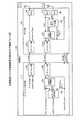
ところで、図7に示した無線装置1の他に、ダイバーシティと呼ばれる技術を利用した無線装置が考案されている。例えば、ダイバーシティは、複数のアンテナで受信した同一の無線信号について、電波状況の優れたアンテナの信号を優先的に用いる技術である。 Incidentally, in addition to the
図10は、ダイバーシティを利用した無線装置の構成を示す図である。図10に示すように、この無線装置2は、ベースバンド処理部30とRF-IC部40を有する。また、ベースバンド処理部30は、インターフェース部30a,30b、DeMUX処理部31を有する。RF-IC部40は、インターフェース部40a,40b、MUX処理部41、DAC42、ADC43,44を有する。なお、図10に示す無線装置2は、各アンテナから受信した信号をRF-IC部40からベースバンド処理部30にワンレーンで転送する。 FIG. 10 is a diagram illustrating a configuration of a wireless device using diversity. As illustrated in FIG. 10, the wireless device 2 includes a
インターフェース部30aは、IQデータや制御データを取得した場合に、取得したデータをLVDS信号に変換することで、Txパスを介して、IQデータや制御データをRF-IC部40に出力する処理部である。 The
インターフェー部30bは、Rxパスを介して、RF-IC部40からLVDS信号を受信し、受信した信号から制御データや各アンテナAnt1,Ant2で受信したIQデータを抽出する処理部である。インターフェース部30bは、各アンテナAnt1,Ant2で受信したIQデータをDeMux処理部31に出力する。また、インターフェース部30bは、制御データを外部の装置に出力する。 The
DeMux処理部31は、アンテナAnt1で受信したIQデータとアンテナAnt2で受信したIQデータに分離し、分離したIQデータを別々に出力する処理部である。 The
インターフェース部40aは、ベースバンド処理部30から、Txパスを介してLVDS信号を取得した場合に、取得したLVDS信号に含まれるIQデータをDAC42に出力する処理部である。 The
インターフェース部40bは、Mux処理部41から出力されるデータや制御データを取得した場合に、取得したデータをLVDS信号に変換することで、Rxパスを介して、IQデータや制御データをベースバンド処理部30に出力する処理部である。 When the
Mux処理部41は、ADC43から出力されるIQデータ(Ant1から受信したIQデータ)とADC44から出力されるIQデータ(Ant2から受信したIQデータ)を合成し、合成したデータをインターフェース部40bに出力する処理部である。 The
DAC42は、インターフェース部40aから出力されるデジタル信号(IQデータ)をアナログ信号に変換し、変換したアナログ信号をアンテナAnt1に出力する処理部である。 The
ADC43は、アンテナAnt1から取得するアナログ信号をデジタル信号(IQデータ)に変換し、変換したデジタル信号をインターフェース部40bに出力する処理部である。ADC44は、アンテナAnt2から取得するアナログ信号をデジタル信号(IQデータ)に変換し、変換したデジタル信号をインターフェース部40bに出力する処理部である。 The
図11は、ダイバーシティワンレーン時のRxパスの通信フォーマットを示す図である。なお、図11の上段は、アンテナAnt1またはアンテナAnt2でデータを受信した場合のRxパスのLVDS信号を示している。このようなシングル受信時において、LVDS信号のビット間隔は、図8と同様のビット間隔(370bit間隔)となる。 FIG. 11 is a diagram illustrating a communication format of the Rx path at the time of diversity one lane. The upper part of FIG. 11 shows an LVDS signal of the Rx path when data is received by the antenna Ant1 or the antenna Ant2. At the time of such single reception, the bit interval of the LVDS signal is the same bit interval (370 bit interval) as in FIG.
図11の下段は、ダイバーシティ時にアンテナAnt1,Ant2のIQデータを多重化して転送し場合のRxパスのLVDS信号を示している。図11の下段に示すように、ダイバーシティワンレーン時において、インターフェース部40bは、アンテナAnt1側とアンテナAnt2側のIQデータを時系列に交互に転送する。また、各LVDS信号のビット間隔は、45bitとなり、シングル受信時のビット間隔よりも狭くなる。 The lower part of FIG. 11 shows an Rx path LVDS signal when IQ data of the antennas Ant1 and Ant2 are multiplexed and transferred at the time of diversity. As shown in the lower part of FIG. 11, at the time of diversity one lane, the
しかしながら、上述した従来の無線装置は、複数のアンテナから受信したIQデータや制御データをワンレーンで転送すると、データ遅延が発生してしまうという問題があった。図12は、従来技術の問題点を説明するための図である。 However, the above-described conventional radio apparatus has a problem that data delay occurs when IQ data and control data received from a plurality of antennas are transferred in one lane. FIG. 12 is a diagram for explaining the problems of the prior art.
図12の下段に示すように、ダイバーシティワンレーン時には、IQデータを含む各LVDS信号の間隔が狭いため、そのまま制御データを挿入して転送することができない。したがって、制御データを転送する場合には、IQデータを含むLVDS信号を遅らせることで制御データを挿入するだけのビット幅を確保する必要がある。図12の中段と下段を比較すると、制御データを挿入したことにより、かかる制御データ以降のIQデータ、制御データに遅延が発生する。 As shown in the lower part of FIG. 12, at the time of diversity one lane, since the interval between the LVDS signals including IQ data is narrow, control data cannot be inserted and transferred as it is. Therefore, when transferring control data, it is necessary to secure a bit width sufficient to insert control data by delaying an LVDS signal including IQ data. Comparing the middle and lower stages of FIG. 12, the insertion of control data causes a delay in IQ data and control data after the control data.
図12で示したようなデータ遅延が発生すると、例えば、受信側から送信側へ転送される制御データに遅延が発生し、制御データの受信を待って処理を行う送信側において、バッファのオーバーフローなどが発生する恐れがある。したがって、データ遅延の問題を解消することが重要な課題となる。 When the data delay as shown in FIG. 12 occurs, for example, a delay occurs in the control data transferred from the reception side to the transmission side. May occur. Therefore, solving the data delay problem is an important issue.
開示の技術は、上記に鑑みてなされたものであって、データ遅延の問題を解消することが出来る無線装置を提供することを目的とする。 The disclosed technology has been made in view of the above, and an object thereof is to provide a wireless device capable of solving the problem of data delay.
この無線装置は、第1のアンテナが受信したデータと第2のアンテナが受信したデータをそれぞれ取得し、前記第1のアンテナが受信したデータと、第2のアンテナが受信したデータの差分値を算出する差分算出部と、前記第1のアンテナが受信したデータと前記差分値を受信部に転送する転送部とを有することを要件とする。 The wireless device acquires data received by the first antenna and data received by the second antenna, respectively, and calculates a difference value between the data received by the first antenna and the data received by the second antenna. It is a requirement to include a difference calculating unit to calculate, a transfer unit that transfers data received by the first antenna and the difference value to the receiving unit.
この無線装置によれば、複数のアンテナから受信したデータをワンレーンで転送しても、データ遅延の発生を防止することが出来る。 According to this radio apparatus, even when data received from a plurality of antennas is transferred in one lane, occurrence of data delay can be prevented.
以下に、本願の開示する無線装置の実施例を図面に基づいて詳細に説明する。なお、この実施例によりこの発明が限定されるものではない。 Hereinafter, embodiments of a wireless device disclosed in the present application will be described in detail with reference to the drawings. Note that the present invention is not limited to the embodiments.
以下の説明では、無線装置が、アンテナAnt1,Ant2を用いて基地局から信号波を受信する場合について説明するがこれに限定されるものではない。無線装置は、アンテナAnt1,Ant2以外のアンテナを用いて基地局から信号波を受信しても良い。 In the following description, a case where the radio apparatus receives signal waves from the base station using the antennas Ant1 and Ant2 will be described, but the present invention is not limited to this. The wireless device may receive a signal wave from the base station using an antenna other than the antennas Ant1 and Ant2.
まず、本実施例にかかる無線装置の概要について説明する。アンテナAnt1,Ant2は、元々基地局から同一の信号波を受信しているため、アンテナAnt1が受信したIQデータとアンテナAnt2が受信したIQデータに大きな差分はなく、互いに相関を持っている。アンテナAnt1,Ant2が受信したIQデータの差分は、伝播路の違いにより生じた位相差等が主な差分となる。 First, an outline of a wireless device according to the present embodiment will be described. Since the antennas Ant1 and Ant2 originally receive the same signal wave from the base station, the IQ data received by the antenna Ant1 and the IQ data received by the antenna Ant2 do not have a large difference and are correlated with each other. The difference between the IQ data received by the antennas Ant1 and Ant2 is mainly the phase difference caused by the difference in propagation path.
そこで、本実施例にかかる無線装置は、RF-IC部側で、アンテナAnt1が受信したIQデータとアンテナAnt2が受信したIQデータの差分値を時系列に算出し、アンテナAnt2にて受信したIQデータの代わりに、差分値をベースバンド処理部側に転送する。そして、無線装置は、ベースバンド処理部側で、差分値とアンテナAnt1のIQデータとを基にして、アンテナAnt2のIQデータを復元する。 Therefore, the radio apparatus according to the present embodiment calculates, on the RF-IC unit side, the difference value between the IQ data received by the antenna Ant1 and the IQ data received by the antenna Ant2 in time series, and the IQ received by the antenna Ant2 Instead of the data, the difference value is transferred to the baseband processing unit side. Then, on the baseband processing unit side, the wireless device restores the IQ data of the antenna Ant2 based on the difference value and the IQ data of the antenna Ant1.
差分値のデータ量は、アンテナAnt2が受信するIQデータと比較して少ない。したがって、無線装置が、複数のアンテナから受信したIQデータや制御データをワンレーンで転送しても、制御データのビット幅を確保できるので、データ遅延の発生を防止することが出来る。 The data amount of the difference value is small compared to the IQ data received by the antenna Ant2. Therefore, even if the wireless device transfers IQ data and control data received from a plurality of antennas over one lane, the bit width of the control data can be ensured, so that occurrence of data delay can be prevented.
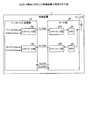
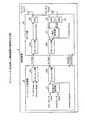
次に、本実施例にかかる無線装置の構成について説明する。図1は、本実施例にかかる無線装置100の構成を示す機能ブロック図である。図1に示すように、この無線装置100は、ベースバンド処理部110と、RF-IC部150を有する。ベースバンド処理部110とRF-IC部150は、従来技術と同様にして、TxパスとRxパスにより相互に接続される。 Next, the configuration of the wireless device according to the present embodiment will be described. FIG. 1 is a functional block diagram of the configuration of the
ベースバンド処理部110は、インターフェース部120a,120b、DeMUX処理部130、IQデータ復元部140を有する。RF-IC部150は、インターフェース部150a,150b、DAC160、ADC170,180、差分データ生成部190、MUX処理部200を有する。 The
ベースバンド処理部110に含まれる各処理部について説明する。インターフェース部120aは、IQデータや制御データを取得した場合に、取得したデータをLVDS信号に変換することで、Txパスを介して、IQデータ(Tx I/Q Data)や制御データ(Control Data)をRF-IC部150に出力する処理部である。 Each processing unit included in the
インターフェース部120bは、Rxパスを介して、RF-IC部150からLVDS信号を受信し、受信した信号から制御データ、差分値(difference Data)、アンテナAnt1で受信したIQデータ(Ant1 Rx I/Q Data)を抽出する処理部である。インターフェース部120bは、アンテナAnt1で受信したIQデータをDeMUX処理部130に出力し、差分値をIQデータ復元部140に出力する。インターフェース部120bは、制御データを外部の装置に出力する。 The
なお、インターフェース部120bは、インターフェース部150bから取得した信号に、アンテナAnt2で受信したIQデータ(Ant2 Rx I/Q Data)が含まれている場合には、アンテナAnt2で受信したIQデータをDeMUX処理部130に出力する。 Note that if the signal acquired from the
DeMUX処理部130は、インターフェース部120bから、アンテナAnt1で受信したIQデータを受信した場合に、受信したIQデータをIQデータ復元部140と外部の装置に出力する処理部である。 The
なお、DeMUX処理部130は、インターフェース部120bから受信したデータに、アンテナAnt1で受信したIQデータとアンテナAnt2で受信したIQデータが含まれる場合には、各IQデータを分離する。そして、DeMUX処理部130は、アンテナAnt1,Ant2で受信した各IQデータをIQデータ復元部140に出力し、アンテナAnt1で受信したIQデータを外部の装置に出力する。 When the data received from the
IQデータ復元部140は、アンテナAnt1のIQデータと差分値を基にして、アンテナAnt2のIQデータを復元する処理部である。例えば、IQデータ復元部140は、アンテナAnt1のIQデータ(時系列に並んだIQデータ)と差分値(時系列に並んだ差分値)を時間毎に対応させて加算することで、アンテナAnt2のIQデータを復元する。 The IQ
IQデータ復元部140は、復元したアンテナAnt2のIQデータを外部の装置に出力する。なお、IQデータ復元部140は、DeMUX処理部130からアンテナAnt2のIQデータを取得した場合には、復元処理を行わず、取得したIQデータを外部の装置に出力する。 The IQ
RF-IC部150に含まれる各処理部について説明する。インターフェース部150aは、ベースバンド処理部110から、Txパスを介してLVDS信号を取得した場合に、取得したLVDS信号に含まれるIQデータをDAC160に出力する処理部である。 Each processing unit included in the RF-
インターフェース部150bは、MUX処理部200から出力されるデータや制御データ、差分値を取得した場合に、取得したデータをLVDS信号に変換することで、Rxパスを介して、IQデータや制御データ、差分値をベースバンド処理部である。 When the
図2は、本実施例にかかるRxパスの通信フォーマットを示す図である。インターフェース部150bは、アンテナAnt1のIQデータを取得した場合には、PayloadにIQデータを格納し、Sync、Headerを付加して、ベースバンド処理部110に転送する。アンテナAnt1のIQデータを転送する場合のビット幅は、280bitとなる。 FIG. 2 is a diagram illustrating a communication format of the Rx path according to the present embodiment. When acquiring the IQ data of the antenna Ant1, the
インターフェース部150bは、差分値を取得した場合には、128bitのPayloadに差分値を格納し、Sync、Headerを付加して、ベースバンド処理部110に転送する。差分値を転送する場合のビット幅は、152bitとなる。 When the
図2に示すように、インターフェース部150bは、IQデータを格納したLVDS信号と差分値を格納したLVDS信号を交互に転送する。図2に示すように、差分値を格納したLVDS信号を転送してから172bitあけて、IQデータを格納したLVDS信号を送信する。かかる172bitのビット幅が存在すれば、IQデータや差分値の転送を遅らせることなく、制御データのLVDS信号(56bit)をベースバンド処理部110に転送することが出来る。 As shown in FIG. 2, the
なお、インターフェース部150bは、MUX処理部200から、アンテナAnt1,Ant2のIQデータを取得した場合には、従来の無線装置と同様にして、アンテナAnt1側とアンテナAnt2側のIQデータを時系列に交互に転送する。 In addition, when the
DAC160は、インターフェース部150aから出力されるデジタル信号(IQデータ)をアナログ信号に変換し、変換したアナログ信号をアンテナAnt1に出力する処理部である。 The
ADC170は、アンテナAnt1から取得するアナログ信号をデジタル信号(IQデータ)に変換し、変換したデジタル信号をMUX処理部200と差分データ生成部190に出力する処理部である。ADC180は、アンテナAnt2から取得するアナログ信号をデジタル信号(IQデータ)に変換し、変換したデジタル信号を差分データ生成部190に出力する処理部である。 The ADC 170 is a processing unit that converts an analog signal acquired from the antenna Ant1 into a digital signal (IQ data), and outputs the converted digital signal to the
差分データ生成部190は、ADC170から取得するIQデータと、ADC180から取得するIQデータとの差分値を時間毎に算出し、算出した差分値をインターフェース部150bに出力する処理部である。なお、差分データ生成部190は、差分値のデータ量が閾値以上の場合には、差分値の代わりに、アンテナAnt2にて受信されたIQデータをMUX処理部200に出力する。 The difference
MUX処理部200は、ADC170からアンテナAnt1のIQデータのみを取得した場合には、アンテナAnt1のIQデータをインターフェース部150bに出力する。また、MUX処理部200は、ADC170からアンテナAnt1のIQデータを取得し、差分データ生成部190からアンテナAnt2のIQデータを取得した場合には、各IQデータを合成し、インターフェース部150bに出力する。 When only the IQ data of the antenna Ant1 is acquired from the ADC 170, the
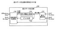
次に、図1に示した差分データ生成部190の構成について説明する。図3は、差分データ生成部190の構成を示す図である。図3に示すように、差分データ生成部190は、差分算出部191、差分閾値比較部192、ビット化部193、送信選択処理部194を有する。 Next, the configuration of the difference
差分算出部191は、ADC170から取得するIQデータと、ADC180から取得するIQデータの差分値を時間毎に算出し、算出した差分値を差分閾値比較部192とビット化部193に出力する処理部である。 The
差分閾値比較部192は、差分値のデータ量と閾値とを比較し、差分値のデータ量が閾値以上となるか否かを判定する処理部である。ここで閾値は、例えば、128bitとする。差分閾値比較部192は、比較結果を送信選択処理部194に出力する。 The difference threshold
ビット化部193は、差分算出部191から差分値を取得した場合に、取得した差分値をビットに変換する処理部である。ビット化部193は、ビットに変換した差分値を送信選択処理部194に出力する。 The
送信選択処理部194は、差分閾値比較部192の比較結果を基にして、差分値またはアンテナAnt2のIQデータをインターフェース部150bに出力する処理部である。具体的に、送信選択処理部194は、差分値のデータ量が閾値以上の場合には、アンテナAnt2のIQデータをインターフェース部150bに出力する。一方、送信選択処理部194は、差分値のデータ量が閾値未満の場合には、差分値をインターフェース部150bに出力する。 The transmission selection processing unit 194 is a processing unit that outputs the difference value or the IQ data of the antenna Ant2 to the
次に、図1に示したIQデータ復元部140の構成について説明する。図4は、IQデータ復元部140の構成を示す図である。図4に示すように、このIQデータ復元部140は、復元処理部141と選択処理部142を有する。 Next, the configuration of the IQ
復元処理部141は、アンテナAnt1のIQデータと差分値を基にして、アンテナAnt2のIQデータを復元する処理部である。例えば、復元処理部141は、アンテナAnt1のIQデータ(時系列に並んだIQデータ)と、差分値(時系列に並んだ差分値)を時間毎に対応させて加算することで、アンテナAnt2のIQデータを復元する。復元処理部141は、復元したアンテナAnt2のIQデータを選択処理部142に出力する。 The
選択処理部142は、復元処理部141から出力されるアンテナAnt2のIQデータ、または、DeMUX処理部130から出力されるアンテナAnt2のIQデータを選択し、選択したIQデータを、アンテナAnt2のIQデータとして、外部の装置に出力する処理部である。 The
選択処理部142は、DeMUX処理部130からアンテナAnt2のIQデータを取得した場合には、かかるIQデータを外部の装置に出力する。一方、選択処理部142は、DeMUX処理部130からアンテナAnt2のIQデータを取得できない場合に、復元処理部141からアンテナAnt2のIQデータを取得し、かかるIQデータを外部の装置に出力する。 When the
次に、本実施例にかかるRF-IC部150の処理手順について説明する。図5は、本実施例にかかるRF-IC部150の処理手順を示すフローチャートである。図5に示すように、RF-IC部150は、アンテナAnt1,Ant2のIQデータを取得し(ステップS101)、各IQデータの差分値を算出する(ステップS102)。 Next, a processing procedure of the RF-
RF-IC部150は、差分値のデータ量が閾値以上か否かを判定する(ステップS103)。RF-IC部150は、差分値のデータ量が閾値未満の場合に(ステップS104,No)、アンテナAnt1のIQデータと差分値をベースバンド処理部110に出力する(ステップS105)。一方、RF-IC部150は、差分値のデータ量が閾値以上の場合に(ステップS104,Yes)、アンテナAnt1,Ant2のIQデータをベースバンド処理部110に出力する(ステップS106)。 The RF-
次に、本実施例にかかるIQデータ復元部140の処理手順について説明する。図6は、本実施例にかかるIQデータ復元部140の処理手順を示すフローチャートである。図6に示すように、IQデータ復元部140は、差分値を取得したか否かを判定する(ステップS201)。 Next, the processing procedure of the IQ
IQデータ復元部140は、差分値を取得している場合には(ステップS202,Yes)、差分値とアンテナAnt2のIQデータを基にしてアンテナAnt2のIQデータを復元し(ステップS203)、アンテナAnt2のIQデータを出力する(ステップS204)。 If the IQ
一方、IQデータ復元部140は、差分値を取得していない場合には(ステップS202,No)、アンテナAnt2のIQデータをDeMUX処理部130から取得し(ステップS205)、ステップS204に移行する。 On the other hand, when the IQ
上述してきたように、本実施例にかかる無線装置100は、RF-IC部150が、アンテナAnt1が受信したIQデータとアンテナAnt2が受信したIQデータの差分値を算出し、アンテナAnt2にて受信したIQデータの代わりに、差分値をベースバンド処理部110に転送する。そして、無線装置100は、ベースバンド処理部110が、差分値とアンテナAnt1のIQデータとを基にして、アンテナAnt2のIQデータを復元する。 As described above, in the
差分値のデータ量は、アンテナAnt2が受信するIQデータと比較して少ない。したがって、無線装置100が、複数のアンテナから受信したIQデータや制御データをワンレーンで転送しても、制御データのビット幅を確保できるので、データ遅延の発生を防止することが出来る。 The data amount of the difference value is small compared to the IQ data received by the antenna Ant2. Therefore, even if the
ところで、本実施例において説明した各処理のうち、自動的におこなわれるものとして説明した処理の全部または一部を手動的におこなうこともでき、あるいは、手動的におこなわれるものとして説明した処理の全部または一部を公知の方法で自動的におこなうこともできる。この他、上記文書中や図面中で示した処理手順、制御手順、具体的名称、各種のデータやパラメータを含む情報については、特記する場合を除いて任意に変更することができる。 By the way, among the processes described in the present embodiment, all or part of the processes described as being automatically performed can be manually performed, or the processes described as being manually performed can be performed. All or a part can be automatically performed by a known method. In addition, the processing procedure, control procedure, specific name, and information including various data and parameters shown in the above-described document and drawings can be arbitrarily changed unless otherwise specified.
以上の各実施例を含む実施形態に関し、さらに以下の付記を開示する。 The following supplementary notes are further disclosed with respect to the embodiments including the above examples.
(付記1)第1のアンテナが受信したデータと第2のアンテナが受信したデータをそれぞれ取得し、前記第1のアンテナが受信したデータと、第2のアンテナが受信したデータの差分値を算出する差分算出部と、
前記第1のアンテナが受信したデータと前記差分値を受信部に転送する転送部と
を有することを特徴とする無線装置。(Supplementary Note 1) Data received by the first antenna and data received by the second antenna are respectively acquired, and a difference value between the data received by the first antenna and the data received by the second antenna is calculated. A difference calculating unit to
A wireless device comprising: a data received by the first antenna; and a transfer unit that transfers the difference value to a receiving unit.
(付記2)前記転送部は、前記第1のアンテナが受信したデータと差分値を信号に変換し、変換した各信号を相互に前記受信部に転送することを特徴とする付記1に記載の無線装置。(Additional remark 2) The said transfer part converts the data and difference value which the said 1st antenna received into a signal, and transfers each converted signal mutually to the said receiving part, The
(付記3)前記転送部は、前記差分値のデータ量と閾値を比較し、前記差分値のデータ量が閾値未満の場合に、前記第1のアンテナが受信したデータと差分値を前記受信部に転送することを特徴とする付記1または2に記載の無線装置。(Additional remark 3) The said transfer part compares the data amount of the said difference value, and a threshold value, and when the data amount of the said difference value is less than a threshold value, the data and difference value which the said 1st antenna received are said receiving part. The wireless device according to
(付記4)前記転送部は、前記差分値のデータ量と閾値を比較し、前記差分値のデータ量が閾値以上の場合に、前記差分値の代わりに、第2のアンテナが受信したデータを前記受信部に送信することを特徴とする付記1、2または3に記載の無線装置。(Additional remark 4) The said transfer part compares the data amount of the said difference value with a threshold value, and when the data amount of the said difference value is more than a threshold value, it uses the data which the 2nd antenna received instead of the said difference value. 4. The wireless device according to
(付記5)前記転送部から、前記第1のアンテナが受信したデータと前記差分値を受信した場合に、前記データと前記差分値を基にして、前記第2のアンテナが受信したデータを復元する復元部を更に有することを特徴とする付記1〜4のいずれか一つに記載の無線装置。(Supplementary Note 5) When the data received by the first antenna and the difference value are received from the transfer unit, the data received by the second antenna is restored based on the data and the difference value. The wireless device according to any one of
(付記6)無線装置が、
第1のアンテナが受信したデータと第2のアンテナが受信したデータをそれぞれ取得し、前記第1のアンテナが受信したデータと、第2のアンテナが受信したデータの差分値を算出する算出ステップと、
前記第1のアンテナが受信したデータと前記差分値を受信部に転送する転送ステップと
を含んだことを特徴とする転送方法。(Appendix 6) The wireless device is
A calculation step of acquiring data received by the first antenna and data received by the second antenna, respectively, and calculating a difference value between the data received by the first antenna and the data received by the second antenna; ,
The transfer method characterized by including the data which the said 1st antenna received, and the transfer step which transfers the said difference value to a receiving part.
(付記7)前記転送ステップは、前記第1のアンテナが受信したデータと差分値を信号に変換し、変換した各信号を相互に前記受信部に転送することを特徴とする付記6に記載の転送方法。(Additional remark 7) The said transfer step converts the data and difference value which the said 1st antenna received into a signal, and transfers each converted signal mutually to the said receiving part, The additional remark 6 characterized by the above-mentioned. Transfer method.
(付記8)前記転送ステップは、前記差分値のデータ量と閾値を比較し、前記差分値のデータ量が閾値未満の場合に、前記第1のアンテナが受信したデータと差分値を前記受信部に転送することを特徴とする付記6または7に記載の転送方法。(Additional remark 8) The said transfer step compares the data amount of the said difference value, and a threshold value, and when the data amount of the said difference value is less than a threshold value, the data and difference value which the said 1st antenna received are said receiving part. The transfer method according to appendix 6 or 7, wherein the transfer method is performed.
(付記9)前記転送ステップは、前記差分値のデータ量と閾値を比較し、前記差分値のデータ量が閾値以上の場合に、前記差分値の代わりに、第2のアンテナが受信したデータを前記受信部に送信することを特徴とする付記6、7または8に記載の転送方法。(Additional remark 9) The said transfer step compares the data amount of the said difference value with a threshold value, and when the data amount of the said difference value is more than a threshold value, it uses the data which the 2nd antenna received instead of the said difference value. 9. The transfer method according to
(付記10)前記第1のアンテナが受信したデータと前記差分値を受信した場合に、前記データと前記差分値を基にして、前記第2のアンテナが受信したデータを復元する復元ステップを更に含んだことを特徴とする付記6〜9のいずれか一つに記載の転送方法。(Supplementary Note 10) A restoration step of restoring the data received by the second antenna based on the data and the difference value when the data and the difference value received by the first antenna are received. The transfer method according to any one of appendices 6 to 9, wherein the transfer method is included.
1,2,100 無線装置
10,110 ベースバンド処理部
11,41,200 Mux処理部
12 P/S変換処理部
13 SyncMux処理部
14 LVDSドライバ
15 LVDSレシーバ
16 サンプリング処理部
17 SyncDetect処理部
18 S/P変換処理部
19 Detect処理部
10a,10b,20a,20b,30a,30b,40a,40b,120a,120b,150a,150b インターフェース部
20,40 RF-IC部
21,42,160 DAC
22,43,44,170,180 ADC
31,130 DeMUX処理部
140 IQデータ復元部
141 復元処理部
142 選択処理部
190 差分データ生成部
191 差分算出部
192 差分閾値比較部
193 ビット化部
194 送信選択処理部1, 2, 100
22, 43, 44, 170, 180 ADC
31, 130
Claims (5)
Translated fromJapanese前記第1のアンテナが受信したデータと前記差分値を受信部に転送する転送部と
を有することを特徴とする無線装置。And data received by the first antennaand the second antenna receives the data respectively acquired,a difference value used in the restoration of data received by the second antenna with the data which the first antenna receives , and data that the first antenna receives a difference calculation unit for calculatingthe differencebetweensaid second antenna has received data,
A wireless device comprising: a data received by the first antenna; and a transfer unit that transfers the difference value to a receiving unit.
Priority Applications (3)
| Application Number | Priority Date | Filing Date | Title |
|---|---|---|---|
| JP2009120191AJP5347709B2 (en) | 2009-05-18 | 2009-05-18 | Wireless device |
| US12/756,297US8588352B2 (en) | 2009-05-18 | 2010-04-08 | Wireless device |
| EP10161226.5AEP2254256B1 (en) | 2009-05-18 | 2010-04-27 | Wireless device |
Applications Claiming Priority (1)
| Application Number | Priority Date | Filing Date | Title |
|---|---|---|---|
| JP2009120191AJP5347709B2 (en) | 2009-05-18 | 2009-05-18 | Wireless device |
Publications (2)
| Publication Number | Publication Date |
|---|---|
| JP2010268395A JP2010268395A (en) | 2010-11-25 |
| JP5347709B2true JP5347709B2 (en) | 2013-11-20 |
Family
ID=42629551
Family Applications (1)
| Application Number | Title | Priority Date | Filing Date |
|---|---|---|---|
| JP2009120191AExpired - Fee RelatedJP5347709B2 (en) | 2009-05-18 | 2009-05-18 | Wireless device |
Country Status (3)
| Country | Link |
|---|---|
| US (1) | US8588352B2 (en) |
| EP (1) | EP2254256B1 (en) |
| JP (1) | JP5347709B2 (en) |
Families Citing this family (7)
| Publication number | Priority date | Publication date | Assignee | Title |
|---|---|---|---|---|
| JP5673388B2 (en) | 2011-06-23 | 2015-02-18 | 富士通株式会社 | Wireless device and wireless communication control program |
| JP5786691B2 (en)* | 2011-12-01 | 2015-09-30 | ソニー株式会社 | Transmission / reception device and transmission / reception system |
| WO2013145313A1 (en) | 2012-03-30 | 2013-10-03 | 富士通株式会社 | Wireless device, baseband processing device, and communication method |
| US8824535B2 (en) | 2012-05-22 | 2014-09-02 | Blackberry Limited | System and method for transmitting data through a digital interface |
| US10530611B1 (en)* | 2013-04-25 | 2020-01-07 | Analog Devices, Inc. | Fast control interface |
| US10567070B2 (en)* | 2017-04-02 | 2020-02-18 | Ahmad Jalali | Air to ground network for broadband access to aerial platforms |
| US20240097727A1 (en)* | 2022-09-16 | 2024-03-21 | Apple Inc. | Electronic Devices with Adjustable Received Sample Bit Width |
Family Cites Families (20)
| Publication number | Priority date | Publication date | Assignee | Title |
|---|---|---|---|---|
| JP2958742B2 (en)* | 1994-10-07 | 1999-10-06 | ローランド株式会社 | Waveform data compression device, waveform data decompression device, quantization device, and data creation method using floating point |
| JP2000209164A (en)* | 1999-01-13 | 2000-07-28 | Nec Corp | Data transmission system |
| US6751264B2 (en)* | 2001-07-27 | 2004-06-15 | Motorola, Inc. | Receiver and method therefor |
| JP3997890B2 (en)* | 2001-11-13 | 2007-10-24 | 松下電器産業株式会社 | Transmission method and transmission apparatus |
| JP2004104379A (en)* | 2002-09-09 | 2004-04-02 | Hitachi Kokusai Electric Inc | Wireless communication device |
| JP2004147082A (en)* | 2002-10-24 | 2004-05-20 | Matsushita Electric Ind Co Ltd | Communication device |
| CN100576772C (en)* | 2002-12-27 | 2009-12-30 | Nxp股份有限公司 | Mobile terminal with smart antenna and method thereof |
| EP1684454A4 (en)* | 2003-11-21 | 2013-07-03 | Panasonic Corp | METHOD, DEVICE, TRANSMISSION APPARATUS AND MULTI-ANTENNA COMMUNICATION SYSTEM |
| CN100541465C (en)* | 2004-09-07 | 2009-09-16 | 飞思卡尔半导体公司 | Device and integrated circuit for generating a plurality of different gate pulse signals |
| US7382313B1 (en)* | 2004-11-03 | 2008-06-03 | Topcon Gps, Llc | Method for absolute calibration of global navigation satellite system antennas |
| JP4884722B2 (en) | 2005-03-31 | 2012-02-29 | 株式会社エヌ・ティ・ティ・ドコモ | Wireless communication apparatus and wireless communication method |
| JP2007096762A (en)* | 2005-09-29 | 2007-04-12 | Toshiba Corp | transceiver |
| WO2007049547A1 (en)* | 2005-10-24 | 2007-05-03 | Matsushita Electric Industrial Co., Ltd. | Interfering signal characterizing quantity storing method and device, interfering signal characterizing quantity acquiring method and device, and interfering signal suppressing method and device |
| US7463871B2 (en)* | 2005-12-09 | 2008-12-09 | Broadcom Corporation | Processing received digital data signals based on a received digital data format |
| US7953439B2 (en)* | 2006-12-19 | 2011-05-31 | Broadcom Corporation | Voice-data-RF integrated circuit |
| US7596356B2 (en)* | 2006-12-19 | 2009-09-29 | Broadcom Corporation | On-chip baseband-to-RF interface and applications thereof |
| US7738491B2 (en)* | 2007-07-16 | 2010-06-15 | Infineon Technologies Ag | Frame structure, method for organizing data and method for transmitting data |
| US8340622B2 (en)* | 2007-08-09 | 2012-12-25 | Freescale Semiconductor, Inc. | Arrangement of radiofrequency integrated circuit and method for manufacturing thereof |
| US9313067B2 (en)* | 2007-08-14 | 2016-04-12 | Qualcomm Incorporated | Multi-bandwidth communication system using a shared baseband processor |
| JP2009076969A (en)* | 2007-09-18 | 2009-04-09 | Olympus Corp | Image processing apparatus |
- 2009
- 2009-05-18JPJP2009120191Apatent/JP5347709B2/ennot_activeExpired - Fee Related
- 2010
- 2010-04-08USUS12/756,297patent/US8588352B2/ennot_activeExpired - Fee Related
- 2010-04-27EPEP10161226.5Apatent/EP2254256B1/ennot_activeNot-in-force
Also Published As
| Publication number | Publication date |
|---|---|
| JP2010268395A (en) | 2010-11-25 |
| EP2254256A2 (en) | 2010-11-24 |
| EP2254256B1 (en) | 2017-04-19 |
| EP2254256A3 (en) | 2014-01-01 |
| US8588352B2 (en) | 2013-11-19 |
| US20100290566A1 (en) | 2010-11-18 |
Similar Documents
| Publication | Publication Date | Title |
|---|---|---|
| JP5347709B2 (en) | Wireless device | |
| EP2583383B1 (en) | Digital distributed antenna system with improved data transmission features | |
| US20200304612A1 (en) | Method of transmitting a data signal in sync with a clock signal | |
| US7869409B2 (en) | System and method for transmitting a multiple format wireless signal | |
| KR101783963B1 (en) | Method and system for chroma partitioning and rate adaptation for uncompressed video transmission in wireless networks | |
| US8594223B2 (en) | Transport data reduction for DAS systems | |
| WO2004001893A3 (en) | Reduced-complexity antenna system using multiplexed receive chain processing | |
| WO2009143176A3 (en) | Compression of signals in base transceiver systems | |
| EP2216909A3 (en) | Digital if distribution network for radio communications | |
| CN102077483B (en) | Signal converter, wireless signal transmission system, and wireless signal reception system | |
| US8768285B2 (en) | Synchronization of front-end and baseband units in wireless communications device by wirelessly transmitting clock signal therebetween | |
| JP4758795B2 (en) | Transmission status display method | |
| WO2012086654A1 (en) | Transmitter, receiver, communication system, and communication method | |
| US7599401B2 (en) | Transmission device and transmission method | |
| KR20090039946A (en) | Apparatus and method for receiving signal in multiple input multiple output system | |
| JP2010154160A (en) | Synchronization detecting circuit, synchronization detection method, and interface circuit | |
| US20160173151A1 (en) | Receiving device, communication system, and interference detection method | |
| JP5359929B2 (en) | Transmission device, reception device, communication system, transmission method, and conversion method | |
| WO2021065915A1 (en) | Frame generation method and frame generation device | |
| US8693572B2 (en) | Method for transmitting signal of orthogonal frequency division multiplexing type, and apparatus applied to the same | |
| JP6025192B2 (en) | Wireless LAN communication device, wireless LAN communication device control program, and wireless LAN communication device control method | |
| JP5182041B2 (en) | Baseband signal processing apparatus and data transmission / reception method | |
| JP4045057B2 (en) | Time diversity circuit using partially retransmitted data | |
| EP3681118B1 (en) | Transmission device, transmission method, reception device, and reception method | |
| JP5474875B2 (en) | Wireless communication system |
Legal Events
| Date | Code | Title | Description |
|---|---|---|---|
| A621 | Written request for application examination | Free format text:JAPANESE INTERMEDIATE CODE: A621 Effective date:20120105 | |
| A977 | Report on retrieval | Free format text:JAPANESE INTERMEDIATE CODE: A971007 Effective date:20120926 | |
| A131 | Notification of reasons for refusal | Free format text:JAPANESE INTERMEDIATE CODE: A131 Effective date:20121009 | |
| A521 | Written amendment | Free format text:JAPANESE INTERMEDIATE CODE: A523 Effective date:20121207 | |
| A131 | Notification of reasons for refusal | Free format text:JAPANESE INTERMEDIATE CODE: A131 Effective date:20130115 | |
| TRDD | Decision of grant or rejection written | ||
| A01 | Written decision to grant a patent or to grant a registration (utility model) | Free format text:JAPANESE INTERMEDIATE CODE: A01 Effective date:20130723 | |
| A61 | First payment of annual fees (during grant procedure) | Free format text:JAPANESE INTERMEDIATE CODE: A61 Effective date:20130805 | |
| R150 | Certificate of patent or registration of utility model | Free format text:JAPANESE INTERMEDIATE CODE: R150 | |
| LAPS | Cancellation because of no payment of annual fees |