JP5346443B2 - Semiconductor light emitting device and manufacturing method thereof - Google Patents
Semiconductor light emitting device and manufacturing method thereofDownload PDFInfo
- Publication number
- JP5346443B2 JP5346443B2JP2007107130AJP2007107130AJP5346443B2JP 5346443 B2JP5346443 B2JP 5346443B2JP 2007107130 AJP2007107130 AJP 2007107130AJP 2007107130 AJP2007107130 AJP 2007107130AJP 5346443 B2JP5346443 B2JP 5346443B2
- Authority
- JP
- Japan
- Prior art keywords
- layer
- metal
- light emitting
- disposed
- semiconductor light
- Prior art date
- Legal status (The legal status is an assumption and is not a legal conclusion. Google has not performed a legal analysis and makes no representation as to the accuracy of the status listed.)
- Active
Links
Images


Classifications
- H—ELECTRICITY
- H10—SEMICONDUCTOR DEVICES; ELECTRIC SOLID-STATE DEVICES NOT OTHERWISE PROVIDED FOR
- H10H—INORGANIC LIGHT-EMITTING SEMICONDUCTOR DEVICES HAVING POTENTIAL BARRIERS
- H10H20/00—Individual inorganic light-emitting semiconductor devices having potential barriers, e.g. light-emitting diodes [LED]
- H10H20/80—Constructional details
- H10H20/81—Bodies
- H10H20/811—Bodies having quantum effect structures or superlattices, e.g. tunnel junctions
- H10H20/812—Bodies having quantum effect structures or superlattices, e.g. tunnel junctions within the light-emitting regions, e.g. having quantum confinement structures
- H—ELECTRICITY
- H10—SEMICONDUCTOR DEVICES; ELECTRIC SOLID-STATE DEVICES NOT OTHERWISE PROVIDED FOR
- H10H—INORGANIC LIGHT-EMITTING SEMICONDUCTOR DEVICES HAVING POTENTIAL BARRIERS
- H10H20/00—Individual inorganic light-emitting semiconductor devices having potential barriers, e.g. light-emitting diodes [LED]
- H10H20/80—Constructional details
- H10H20/81—Bodies
- H10H20/814—Bodies having reflecting means, e.g. semiconductor Bragg reflectors
- H—ELECTRICITY
- H10—SEMICONDUCTOR DEVICES; ELECTRIC SOLID-STATE DEVICES NOT OTHERWISE PROVIDED FOR
- H10H—INORGANIC LIGHT-EMITTING SEMICONDUCTOR DEVICES HAVING POTENTIAL BARRIERS
- H10H20/00—Individual inorganic light-emitting semiconductor devices having potential barriers, e.g. light-emitting diodes [LED]
- H10H20/80—Constructional details
- H10H20/81—Bodies
- H10H20/816—Bodies having carrier transport control structures, e.g. highly-doped semiconductor layers or current-blocking structures
- H10H20/8162—Current-blocking structures
- H—ELECTRICITY
- H10—SEMICONDUCTOR DEVICES; ELECTRIC SOLID-STATE DEVICES NOT OTHERWISE PROVIDED FOR
- H10H—INORGANIC LIGHT-EMITTING SEMICONDUCTOR DEVICES HAVING POTENTIAL BARRIERS
- H10H20/00—Individual inorganic light-emitting semiconductor devices having potential barriers, e.g. light-emitting diodes [LED]
- H10H20/80—Constructional details
- H10H20/81—Bodies
- H10H20/819—Bodies characterised by their shape, e.g. curved or truncated substrates
- H10H20/82—Roughened surfaces, e.g. at the interface between epitaxial layers
- H—ELECTRICITY
- H10—SEMICONDUCTOR DEVICES; ELECTRIC SOLID-STATE DEVICES NOT OTHERWISE PROVIDED FOR
- H10H—INORGANIC LIGHT-EMITTING SEMICONDUCTOR DEVICES HAVING POTENTIAL BARRIERS
- H10H20/00—Individual inorganic light-emitting semiconductor devices having potential barriers, e.g. light-emitting diodes [LED]
- H10H20/80—Constructional details
- H10H20/81—Bodies
- H10H20/822—Materials of the light-emitting regions
- H10H20/824—Materials of the light-emitting regions comprising only Group III-V materials, e.g. GaP
- H—ELECTRICITY
- H10—SEMICONDUCTOR DEVICES; ELECTRIC SOLID-STATE DEVICES NOT OTHERWISE PROVIDED FOR
- H10H—INORGANIC LIGHT-EMITTING SEMICONDUCTOR DEVICES HAVING POTENTIAL BARRIERS
- H10H20/00—Individual inorganic light-emitting semiconductor devices having potential barriers, e.g. light-emitting diodes [LED]
- H10H20/80—Constructional details
- H10H20/83—Electrodes
- H10H20/832—Electrodes characterised by their material
- H10H20/835—Reflective materials
- H—ELECTRICITY
- H10—SEMICONDUCTOR DEVICES; ELECTRIC SOLID-STATE DEVICES NOT OTHERWISE PROVIDED FOR
- H10H—INORGANIC LIGHT-EMITTING SEMICONDUCTOR DEVICES HAVING POTENTIAL BARRIERS
- H10H20/00—Individual inorganic light-emitting semiconductor devices having potential barriers, e.g. light-emitting diodes [LED]
- H10H20/80—Constructional details
- H10H20/84—Coatings, e.g. passivation layers or antireflective coatings
- H10H20/841—Reflective coatings, e.g. dielectric Bragg reflectors
- H—ELECTRICITY
- H10—SEMICONDUCTOR DEVICES; ELECTRIC SOLID-STATE DEVICES NOT OTHERWISE PROVIDED FOR
- H10H—INORGANIC LIGHT-EMITTING SEMICONDUCTOR DEVICES HAVING POTENTIAL BARRIERS
- H10H20/00—Individual inorganic light-emitting semiconductor devices having potential barriers, e.g. light-emitting diodes [LED]
- H10H20/80—Constructional details
- H10H20/85—Packages
- H10H20/855—Optical field-shaping means, e.g. lenses
- H10H20/856—Reflecting means
Landscapes
- Led Devices (AREA)
Abstract
Description
Translated fromJapanese本発明は、半導体発光素子およびその製造方法に関し、特に、金属反射層を備える発光ダイオードと不透明基板層をウェハボンディング技術によって、貼り付けて形成することを特徴とする半導体発光素子およびその製造方法に関する。 The present invention relates to a semiconductor light emitting device and a method for manufacturing the same, and more particularly, to a semiconductor light emitting device and a method for manufacturing the same, wherein a light emitting diode having a metal reflection layer and an opaque substrate layer are attached by wafer bonding technology. .
発光ダイオード(LED:Light Emitting Diode)を高輝度化するために、光の反射層として、基板と、多重量子井戸(MQW:Multi-Quantum Well)層からなる活性層との間に金属反射層を形成する構造が提案されている。このような金属反射層を形成する方法として、例えば、発光ダイオード層の基板のウェハボンディング(貼付け)技術が開示されている(例えば、特許文献1および特許文献2参照。)。 In order to increase the brightness of a light emitting diode (LED), a metal reflection layer is provided as a light reflection layer between a substrate and an active layer composed of a multi-quantum well (MQW) layer. The structure to be formed has been proposed. As a method for forming such a metal reflective layer, for example, a wafer bonding (sticking) technique for a substrate of a light emitting diode layer has been disclosed (see, for example, Patent Document 1 and Patent Document 2).
特許文献1および特許文献2は、所望の機械的特性と透光性を有する発光ダイオードを製造することができ、かつ透明層と成長層との境界面の抵抗率を最小限にすることができる発光ダイオードの製造方法を提供することを目的とし、一時的成長基板上に発光ダイオード層を順次成長させ、比較的薄い層の発光ダイオード構造を形成後、一時的成長基板を除去し、一時的成長基板に代えてその位置に下層の緩衝層となる発光ダイオード層に導電性、透光性基板をウェハボンディングして発光ダイオードを製造することを特徴とする。特許文献1および特許文献2においては、貼付けに用いる基板にはGaPやサファイア等の透明なものを適用している。 Patent Document 1 and
図23乃至図25は、ウェハボンディング技術により形成した従来の半導体発光素子の模式的断面構造を示す。 23 to 25 show a schematic cross-sectional structure of a conventional semiconductor light emitting device formed by wafer bonding technology.
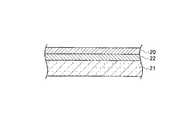
例えば、従来の半導体発光素子は、図23に示すように、GaAs基板15上に配置されたAu-Sn合金層14と、Au-Sn合金層14上に配置されたバリアメタル層13と、バリアメタル層13上に配置されたp型クラッド層10と、p型クラッド層10上に配置されたMQW層9と、MQW層9上に配置されたn型クラッド層8と、n型クラッド層8上に配置されたウィンドウ層7とを備える。 For example, as shown in FIG. 23, a conventional semiconductor light emitting device includes an Au—
図23に示す従来の半導体発光素子は、貼付けに使われる金属は、Au−Sn合金である。このAu−Sn合金は融点が低いため、低温でLEDを構成するエピタキシャル成長層側のAu−Sn合金とGaAs基板15側のAu−Sn合金が溶け、貼り付けることができる。 In the conventional semiconductor light emitting device shown in FIG. 23, the metal used for pasting is an Au—Sn alloy. Since the Au—Sn alloy has a low melting point, the Au—Sn alloy on the epitaxial growth layer side and the Au—Sn alloy on the
しかし、Au−Sn合金層14を使用する場合、Snの熱拡散が起こるため、Snの拡散を防ぐために、図23に示すように、バリアメタル層13を入れる必要がある。また、Au−Sn合金層14は光の反射率が悪いという問題点がある。 However, when the Au—
例えば、従来の別の半導体発光素子は、図24に示すように、GaAs基板15上に配置された金属反射層16と、金属反射層16上に配置されたp型クラッド層10と、p型クラッド層10上に配置されたMQW層9と、MQW層9上に配置されたn型クラッド層8と、n型クラッド層8上に配置されたウィンドウ層7とを備える。図24に示す従来の半導体発光素子は、GaAs基板15を貼り付けて作った金属反射層16では、金属と半導体との界面で光の吸収が起こり、効率よく光を反射することができないという問題点がある。すなわち、p型クラッド層10と金属反射層16の界面で光の吸収が起こるという問題点がある。 For example, as shown in FIG. 24, another conventional semiconductor light emitting device includes a
半導体発光素子(LED)を高輝度化するには、光の反射層としてGaAs基板と活性層(MQW)の間に分布ブラック反射(DBR:Distributed Bragg Reflector)層を入れる方法もある。DBRを入れない構造のLEDでは、MQW層で発光した光がGaAs基板に吸収されてしまうために暗くなる。そのため、GaAs基板を用いるLEDを高輝度化するために、光の反射層としてDBRが用いられている。 In order to increase the brightness of a semiconductor light emitting device (LED), there is also a method in which a distributed black reflection (DBR) layer is provided between a GaAs substrate and an active layer (MQW) as a light reflection layer. In an LED without a DBR structure, light emitted from the MQW layer is absorbed by the GaAs substrate and becomes dark. Therefore, DBR is used as a light reflection layer in order to increase the brightness of LEDs using a GaAs substrate.
すなわち、従来の更に別の半導体発光素子は、図25に示すように、GaAs基板15上に配置されたDBR層19と、DBR層19上に配置されたp型クラッド層10と、p型クラッド層10上に配置されたMQW層9と、MQW層9上に配置されたn型クラッド層8と、n型クラッド層8上に配置されたウィンドウ層7とを備える。図25に示す従来の半導体発光素子は、GaAs基板15とMQW層9との間に光の反射層としてDBR層19を用いているが、DBR層19はある一方向から入射した光のみ反射し、入射角が変わるとDBRは光を反射せず、それ以外の角度から入射した光はDBR層19で反射せず透過してしまうという問題点がある。そのため、透過した光はGaAs基板15に吸収されてしまい、半導体発光素子(LED)の発光輝度が低下するという問題点がある。
ウェハボンディング技術により形成した従来の半導体発光素子は、貼付けに使われる金属としてAu−Sn合金層を使用する場合、Snの熱拡散を防ぐために、バリアメタル層を入れる必要がある。また、Au−Sn合金層は光の反射率が悪い。 When a conventional semiconductor light emitting device formed by wafer bonding technology uses an Au—Sn alloy layer as a metal used for pasting, it is necessary to insert a barrier metal layer in order to prevent thermal diffusion of Sn. Further, the Au—Sn alloy layer has poor light reflectivity.
また、基板を貼り付けることによって金属反射層を形成したとしても、金属と半導体の界面で光の吸収が起こり、効率よく光を反射することができない。 Even if the metal reflective layer is formed by attaching the substrate, light absorption occurs at the interface between the metal and the semiconductor, and light cannot be efficiently reflected.
また、反射層としてDBR層を用いている場合、DBR層はある一方向から入射した光のみ反射し、入射角が変わるとDBR層で反射せず透過してしまい、GaAs基板に吸収されてしまい、LEDの発光輝度が低下する。 In addition, when a DBR layer is used as the reflective layer, the DBR layer reflects only light incident from one direction, and if the incident angle changes, it is transmitted without being reflected by the DBR layer and absorbed by the GaAs substrate. , LED emission brightness decreases.
そこで、本発明の目的は、GaAsやSi等の不透明な半導体基板を用いて、基板の貼付けを行い、金属反射層を形成して高輝度の半導体発光素子およびその製造方法を提供することにある。 Accordingly, an object of the present invention is to provide a high-luminance semiconductor light-emitting device and a method for manufacturing the same by pasting the substrate using an opaque semiconductor substrate such as GaAs or Si and forming a metal reflective layer. .
また、本発明の目的は、金属と半導体との間に透明な絶縁膜を入れることにより、半導体と金属との接触を避け、半導体と金属との界面での光の吸収を防ぎ、反射率の良い金属反射層を形成した、高輝度の半導体発光素子およびその製造方法を提供することにある。 Another object of the present invention is to prevent contact between the semiconductor and the metal by inserting a transparent insulating film between the metal and the semiconductor, prevent light absorption at the interface between the semiconductor and the metal, and improve the reflectance. An object of the present invention is to provide a high-luminance semiconductor light-emitting device having a good metal reflection layer and a method for manufacturing the same.
また、本発明の目的は、光の反射層にDBRではなく、金属層を用いて、あらゆる角度の光を反射させることが可能となり、高輝度の半導体発光素子およびその製造方法を提供することにある。 It is another object of the present invention to provide a high-intensity semiconductor light emitting device and a method for manufacturing the same, by using a metal layer instead of a DBR as a light reflection layer and reflecting light at any angle. is there.
上記目的を達成するための本発明の半導体発光素子の一態様は、GaAs層と、前記GaAs層の表面に配置された第1金属バッファ層と、前記第1金属バッファ層上に配置された第1金属層と、前記GaAs層の裏面に配置された第2金属バッファ層と、前記第2金属バッファ層の前記GaAs層と反対側の表面に配置された第2金属層とを備えるGaAs基板構造と、前記GaAs基板構造上に配置され、第3金属層と、前記第3金属層上に配置される金属コンタクト層と、前記金属コンタクト層上に配置されるp型クラッド層と、前記p型クラッド層に配置される多重量子井戸層と、前記多重量子井戸層上に配置されるn型クラッド層と、前記n型クラッド層上に配置されるウィンドウ層を備える発光ダイオード構造とから構成され、前記第1金属層および前記第3金属層は、いずれもAu層で形成され、前記第1金属層および前記第3金属層を用いて、前記GaAs基板構造と、前記発光ダイオード構造を貼り付け、前記発光ダイオード構造は、前記第3金属層と前記p型クラッド層との間に、前記金属コンタクト層と略同じ厚みであって、パターニングされた開口部を有する絶縁層を含み、前記絶縁層の前記開口部に前記金属コンタクト層が形成されており、前記金属コンタクト層は、Auを含む金属からなり、前記多重量子井戸層は、GaAs/GaAlAs層からなるヘテロ接合ペアを積層した多重量子井戸構造からなり、前記絶縁層は、前記多重量子井戸層からの発光波長に対して透明であることを特徴とする。In order to achieve the above object, one embodiment of a semiconductor light emitting device of the present invention includes a GaAs layer, a first metal buffer layer disposed on the surface of the GaAs layer, and a first metal buffer layer disposed on the first metal buffer layer. A GaAs substrate structure comprising: one metal layer; a second metal buffer layer disposed on the back surface of the GaAs layer; and a second metal layer disposed on the surface of the second metal buffer layer opposite to the GaAs layer. A third metal layer disposed on the GaAs substrate structure; a metal contact layer disposed on the third metal layer; a p-type cladding layer disposed on the metal contact layer; and the p-type A light emitting diode structure including a multiple quantum well layer disposed on the cladding layer, an n-type cladding layer disposed on the multiple quantum well layer, and a window layer disposed on the n-type cladding layer; Serial first metal layer and the third metal layer are both formed of an Au layer, using the first metal layer and the third metal layer, affixed with the GaAs substrate structure, the light emitting diodestructure, The light emitting diode structure includes an insulating layer between the third metal layer and the p-type cladding layer, having an approximately same thickness as the metal contact layer and having a patterned opening, The metal contact layer is formed in the opening, the metal contact layer is made of a metal containing Au, and the multiple quantum well layer is a multi-quantum well structure in which heterojunction pairs made of GaAs / GaAlAs layers are stacked. The insulating layer is transparent to the emission wavelength from the multiple quantum well layer .
本発明の半導体発光素子の他の態様は、GaAs基板と、前記GaAs基板上に配置される金属層と、前記金属層上に配置され,パターニングされた金属コンタクト層および絶縁層と、パターニングされた前記金属コンタクト層および前記絶縁層上に配置されるp型クラッド層10と、前記p型クラッド層上に配置される多重量子井戸層と、前記多重量子井戸層上に配置されるn型クラッド層と、前記n型クラッド層上に配置されるウィンドウ層を備える発光ダイオード構造とから構成され、前記金属層を用いて、前記GaAs基板と、前記発光ダイオード構造を貼り付け、前記金属コンタクト層は、所定のパターン構造が所定の間隔で配置されており、前記金属コンタクト層のパターン幅は5μm〜11μmであり、前記絶縁層は、前記金属コンタクト層と略同じ厚みであって、パターニングされた開口部を有し、前記絶縁層の前記開口部に前記金属コンタクト層が形成されており、前記金属コンタクト層は、Auを含む金属からなり、前記多重量子井戸層は、GaAs/GaAlAs層からなるヘテロ接合ペアを積層した多重量子井戸構造からなり、前記絶縁層は、前記多重量子井戸層からの発光波長に対して透明であることを特徴とする。According to another aspect of the semiconductor light emitting device of the present invention, a patterned GaAs substrate, a metal layer disposed on the GaAs substrate, a patterned metal contact layer and an insulating layer disposed on the metal layer, and patterned A p-
本発明の半導体発光素子の他の態様は、GaAs基板と、前記GaAs基板の表面に配置された第1金属層とを備えるGaAs基板構造と、当該GaAs基板構造上に配置され、第2金属層と、前記第2金属層上に配置されるp型クラッド層と、前記p型クラッド層上に配置される多重量子井戸層と、前記多重量子井戸層上に配置されるn型クラッド層と、前記n型クラッド層上に配置されるウィンドウ層を備える発光ダイオード構造とから構成され、前記第1金属層および前記第2金属層は、いずれもAu層で形成され、前記第1金属層および前記第2金属層を用いて、前記GaAs基板と、前記発光ダイオード構造を貼り付け、前記発光ダイオード構造は、前記第2金属層と前記p型クラッド層との間に、前記金属コンタクト層と略同じ厚みであって、パターニングされた開口部を有する絶縁層を含み、前記絶縁層の前記開口部に前記金属コンタクト層が形成されており、前記金属コンタクト層は、Auを含む金属からなり、前記多重量子井戸層は、GaAs/GaAlAs層からなるヘテロ接合ペアを積層した多重量子井戸構造からなり、前記絶縁層は、前記多重量子井戸層からの発光波長に対して透明であることを特徴とする。According to another aspect of the semiconductor light emitting device of the present invention, a GaAs substrate structure comprising a GaAs substrate and a first metal layer disposed on the surface of the GaAs substrate, and a second metal layer disposed on the GaAs substrate structure. A p-type cladding layer disposed on the second metal layer, a multiple quantum well layer disposed on the p-type cladding layer, an n-type cladding layer disposed on the multiple quantum well layer, A light emitting diode structure including a window layer disposed on the n-type cladding layer, wherein the first metal layer and the second metal layer are both formed of an Au layer, and the first metal layer and the second metal layer using the second metal layer, wherein the GaAs substrate, adhered the light emitting diodestructure, the light emitting diode structure, between the p-type cladding layer and the second metal layer, substantially the same as the metal contact layer An insulating layer having a patterned opening, wherein the metal contact layer is formed in the opening of the insulating layer, and the metal contact layer is made of a metal containing Au, and The quantum well layer has a multiple quantum well structure in which heterojunction pairs made of GaAs / GaAlAs layers are stacked, and the insulating layer is transparent to an emission wavelength from the multiple quantum well layer .
本発明の半導体発光素子の他の態様は、シリコン基板と、前記シリコン基板上に配置されるチタン層と、前記チタン層上に配置される第1金属層とから構成されるシリコン基板構造と、前記第1金属層上に配置される第2金属層と、前記第2金属層上に配置され,パターニングされた金属コンタクト層および絶縁層と、パターニングされた前記金属コンタクト層および前記絶縁層上に配置され,露出された表面にフロスト処理領域を有するエピタキシャル成長層と、前記エピタキシャル成長層上に配置され,パターニングされたn型GaAs層と、前記n型GaAs層上に配置され,パターニングされた表面電極層とから構成されるLED構造とを備え、前記第1金属層および前記第2金属層を用いて、前記シリコン基板構造と、前記発光ダイオード構造を貼り付け、前記金属コンタクト層は、所定のパターン構造が所定の間隔で配置されており、前記金属コンタクト層のパターン幅は5μm〜11μmであり、前記絶縁層は、前記金属コンタクト層と略同じ厚みであって、パターニングされた開口部を有し、前記絶縁層の前記開口部に前記金属コンタクト層が形成されており、前記金属コンタクト層は、Auを含む金属からなり、前記エピタキシャル成長層は、GaAs/GaAlAs層からなるヘテロ接合ペアを積層した多重量子井戸構造からなる多重量子井戸層を含み、前記絶縁層は、前記多重量子井戸層からの発光波長に対して透明であることを特徴とする。Another aspect of the semiconductor light emitting device of the present invention is a silicon substrate structure comprising a silicon substrate, a titanium layer disposed on the silicon substrate, and a first metal layer disposed on the titanium layer, A second metal layer disposed on the first metal layer; a patterned metal contact layer and insulating layer disposed on the second metal layer; and the patterned metal contact layer and insulating layer. An epitaxially grown layer having a frosted region disposed on the exposed surface, an n-type GaAs layer disposed on the epitaxially grown layer and patterned, and a surface electrode layer disposed on the n-type GaAs layer and patterned An LED structure including the silicon substrate structure and the light emitting diode using the first metal layer and the second metal layer. Paste diode structure, the metal contact layer is a predetermined pattern structure are arranged at predetermined intervals, the pattern width of the metal contact layerRi 5μm~11μmder, the insulating layer, the metal contact layer The metal contact layer is formed in the opening of the insulating layer, the metal contact layer is made of a metal containing Au, and the epitaxial growth is performed. The layer includes a multiple quantum well layer having a multiple quantum well structure in which heterojunction pairs made of GaAs / GaAlAs layers are stacked, and the insulating layer is transparent to an emission wavelength from the multiple quantum well layer. Features.
本発明の半導体発光素子の他の態様は、GaAs基板と、前記GaAs基板上に配置される金属バッファ層と、前記金属バッファ層上に配置される第1金属層とから構成されるGaAs基板構造と、前記第1金属層上に配置される第2金属層と、前記第2金属層上に配置され,パターニングされた金属コンタクト層および絶縁層と、パターニングされた前記金属コンタクト層および前記絶縁層上に配置され,露出された表面にフロスト処理領域を有するエピタキシャル成長層と、前記エピタキシャル成長層上に配置され,パターニングされたn型GaAs層と、前記n型GaAs層上に配置され,パターニングされた表面電極層とから構成されるLED構造を備え、前記第1金属層および前記第2金属層を用いて、前記GaAs基板構造と、前記発光ダイオード構造を貼り付け、前記金属コンタクト層は、所定のパターン構造が所定の間隔で配置されており、前記金属コンタクト層のパターン幅は5μm〜11μmであり、前記絶縁層は、前記金属コンタクト層と略同じ厚みであって、パターニングされた開口部を有し、前記絶縁層の前記開口部に前記金属コンタクト層が形成されており、前記金属コンタクト層は、Auを含む金属からなり、前記エピタキシャル成長層は、GaAs/GaAlAs層からなるヘテロ接合ペアを積層した多重量子井戸構造からなる多重量子井戸層を含み、前記絶縁層は、前記多重量子井戸層からの発光波長に対して透明であることを特徴とする。Another aspect of the semiconductor light emitting device of the present invention is a GaAs substrate structure comprising a GaAs substrate, a metal buffer layer disposed on the GaAs substrate, and a first metal layer disposed on the metal buffer layer. A second metal layer disposed on the first metal layer, a patterned metal contact layer and insulating layer disposed on the second metal layer, and the patterned metal contact layer and insulating layer. An epitaxially grown layer having a frosted region disposed on the exposed surface, an n-type GaAs layer disposed on and patterned on the epitaxially grown layer, and a patterned surface disposed on the n-type GaAs layer An LED structure comprising an electrode layer, and using the first metal layer and the second metal layer, the GaAs substrate structure; Serial paste emitting diode structure, the metal contact layer is a predetermined pattern structure are arranged at predetermined intervals, the pattern width of the metal contact layerRi 5μm~11μmder, the insulating layer, the metal It has substantially the same thickness as the contact layer, has a patterned opening, and the metal contact layer is formed in the opening of the insulating layer, and the metal contact layer is made of a metal containing Au, The epitaxially grown layer includes a multiple quantum well layer having a multiple quantum well structure in which heterojunction pairs made of GaAs / GaAlAs layers are stacked, and the insulating layer is transparent to an emission wavelength from the multiple quantum well layer. It is characterized by that.
本発明の半導体発光素子の製造方法の一態様は、貼付け用の半導体基板構造、および貼付け用の発光ダイオード構造を準備する工程と、半導体基板構造においては、半導体基板上に第1金属層を形成する工程と、発光ダイオード構造においては、GaAs基板上のAlInGaP層、n型GaAs層、エピタキシャル成長層を順次形成する工程と、前記エピタキシャル成長層上に、パターニングされた絶縁層に対して、金属コンタクト層および第2金属層を形成する工程と、前記貼付け用の半導体基板構造、および前記貼付け用のLED構造を熱圧着により貼り付ける工程と、前記GaAs基板をエッチングにより除去する工程と、前記AlInGaP層を除去する工程と、表面電極層をパターン形成する工程と、フロスト処理を実施して、表面電極層の直下のn型GaAs層以外のn型GaAs層の除去を行う工程とを有し、前記金属コンタクト層は、所定のパターン構造が所定の間隔で配置されており、前記金属コンタクト層のパターン幅は5μm〜11μmであり、前記絶縁層は、前記金属コンタクト層と略同じ厚みであって、パターニングされた開口部を有し、前記絶縁層の前記開口部に前記金属コンタクト層が形成されており、前記金属コンタクト層は、Auを含む金属からなり、前記エピタキシャル成長層は、GaAs/GaAlAs層からなるヘテロ接合ペアを積層した多重量子井戸構造からなる多重量子井戸層を含み、前記絶縁層は、前記多重量子井戸層からの発光波長に対して透明であることを特徴とする。One aspect of a method for producing a semiconductor light emitting device of the present invention includes a step of preparing a semiconductor substrate structure for pasting and a light emitting diode structure for pasting, and in the semiconductor substrate structure, a first metal layer is formed on the semiconductor substrate. A step of sequentially forming an AlInGaP layer, an n-type GaAs layer, and an epitaxial growth layer on a GaAs substrate, and a metal contact layer and a patterned insulating layer on the epitaxial growth layer. A step of forming a second metal layer, a step of attaching the semiconductor substrate structure for pasting and the LED structure for pasting by thermocompression bonding, a step of removing the GaAs substrate by etching, and removing theAlInGaP layer Performing the process, patterning the surface electrode layer, and frosting, A step of removing an n-type GaAs layer other than the n-type GaAs layer directly under the surface electrode layer, wherein the metal contact layer has a predetermined pattern structure arranged at a predetermined interval, and the metal contact layer pattern width ofRi 5μm~11μmder, the insulating layer is a thickness substantially the same as the metal contact layer has a patterned opening, said metal contact layer on the opening of the insulating layer The metal contact layer is made of a metal containing Au, and the epitaxial growth layer includes a multiple quantum well layer having a multiple quantum well structure in which heterojunction pairs made of GaAs / GaAlAs layers are stacked, and the insulating layer The layer is transparent to the emission wavelength from the multiple quantum well layer .
本発明の半導体発光素子およびその製造方法によれば、Au−Sn合金層によるSn拡散の問題を解決するために、Auからなる金属層を用いてエピタキシャル成長層と半導体基板を貼り付けることにより、バリアメタルが不要となり、Auからなる金属層を用いることで光の反射率の良い金属反射層をLED側の構造に形成することができるので、LEDの高輝度化を図ることができる。 According to the semiconductor light emitting device and the manufacturing method thereof of the present invention, in order to solve the problem of Sn diffusion due to the Au—Sn alloy layer, the barrier layer is formed by attaching the epitaxial growth layer and the semiconductor substrate using a metal layer made of Au. Since no metal is required and a metal reflective layer with good light reflectivity can be formed in the LED side structure by using a metal layer made of Au, the brightness of the LED can be increased.
本発明の半導体発光素子およびその製造方法によれば、金属反射層と半導体層との間に透明な絶縁膜を入れることにより、半導体層と金属反射層との接触を避け、半導体層と金属反射層との界面における光の吸収を防ぎ、反射率の良い金属反射層を形成することができるので、LEDの高輝度化を図ることができる。 According to the semiconductor light emitting device and the method for manufacturing the same of the present invention, by placing a transparent insulating film between the metal reflective layer and the semiconductor layer, contact between the semiconductor layer and the metal reflective layer is avoided, and the semiconductor layer and the metal reflective are Since light absorption at the interface with the layer can be prevented and a metal reflective layer with good reflectance can be formed, the brightness of the LED can be increased.
本発明の半導体発光素子およびその製造方法によれば、GaAs基板への光の吸収を防ぐために、反射層に金属を用いて光を全反射させ、GaAs基板への吸収を防ぎ、あらゆる角度の光を反射することが可能になるので、LEDを高輝度化することができる。 According to the semiconductor light emitting device and the method of manufacturing the same of the present invention, in order to prevent the light absorption to the GaAs substrate, the reflection layer is made of a metal to totally reflect the light to prevent the light absorption at the GaAs substrate. Can be reflected, so that the brightness of the LED can be increased.
次に、図面を参照して、本発明の実施の形態を説明する。以下の図面の記載において、同一または類似の部分には同一または類似の符号を付している。ただし、図面は模式的なものであり、現実のものとは異なることに留意すべきである。また、図面相互間においても互いの寸法の関係や比率が異なる部分が含まれていることはもちろんである。 Next, embodiments of the present invention will be described with reference to the drawings. In the following description of the drawings, the same or similar parts are denoted by the same or similar reference numerals. However, it should be noted that the drawings are schematic and different from the actual ones. Moreover, it is a matter of course that portions having different dimensional relationships and ratios are included between the drawings.
また、以下に示す実施の形態は、この発明の技術的思想を具体化するための装置や方法を例示するものであって、この発明の技術的思想は、各構成部品の配置などを下記のものに特定するものでない。この発明の技術的思想は、特許請求の範囲において、種々の変更を加えることができる。 Further, the embodiment described below exemplifies an apparatus and a method for embodying the technical idea of the present invention. The technical idea of the present invention is the arrangement of each component as described below. It is not something specific. The technical idea of the present invention can be variously modified within the scope of the claims.
[第1の実施の形態]
(素子構造)
本発明の第1の実施の形態に係る半導体発光素子およびその製造方法に適用されるGaAs基板の導電型としては、p型、n型のいずれにおいても適用可能である。図1は、本発明の第1の実施の形態に係る半導体発光素子およびその製造方法に適用されるp型GaAs基板の模式的断面構造を示し、図2は、n型GaAs基板の模式的断面構造を示す。また、図3は、本発明の第1の実施の形態に係る半導体発光素子およびその製造方法に適用されるLEDの模式的断面構造を示す。[First embodiment]
(Element structure)
The conductivity type of the GaAs substrate applied to the semiconductor light emitting device and the manufacturing method thereof according to the first embodiment of the present invention can be applied to either p-type or n-type. FIG. 1 shows a schematic cross-sectional structure of a p-type GaAs substrate applied to the semiconductor light emitting device and the manufacturing method thereof according to the first embodiment of the present invention, and FIG. 2 shows a schematic cross-section of the n-type GaAs substrate. The structure is shown. FIG. 3 shows a schematic cross-sectional structure of an LED applied to the semiconductor light emitting device and the manufacturing method thereof according to the first embodiment of the present invention.
図4は、図1乃至図2に示したp型乃至n型GaAs基板と、図3に示したLEDをウェハボンディング技術によって互いに貼り付けて形成した本発明の第1の実施の形態に係る半導体発光素子の模式的断面構造を示す。 FIG. 4 shows a semiconductor according to the first embodiment of the present invention formed by bonding the p-type to n-type GaAs substrate shown in FIGS. 1 and 2 and the LED shown in FIG. 3 to each other by a wafer bonding technique. 1 shows a schematic cross-sectional structure of a light-emitting element.
本発明の第1の実施の形態に係る半導体発光素子およびその製造方法に適用されるp型GaAs基板は、図1に示すように、p型GaAs層3と、p型GaAs層3の表面に配置された金属バッファ層2と、金属バッファ層2上に配置された金属層1と、p型GaAs層3の裏面に配置された金属バッファ層4と、金属バッファ層4のp型GaAs層3と反対側の表面に配置された金属層5とを備える。 As shown in FIG. 1, the p-type GaAs substrate applied to the semiconductor light emitting device and the manufacturing method thereof according to the first embodiment of the present invention is formed on the p-
本発明の第1の実施の形態に係る半導体発光素子およびその製造方法に適用されるn型GaAs基板は、図2に示すように、n型GaAs層6と、n型GaAs層6の表面に配置された金属バッファ層2と、金属バッファ層2上に配置された金属層1と、n型GaAs層6の裏面に配置された金属バッファ層4と、金属バッファ層4のn型GaAs層6と反対側の表面に配置された金属層5とを備える。 The n-type GaAs substrate applied to the semiconductor light emitting device and the manufacturing method thereof according to the first embodiment of the present invention has an n-
図1の構造において、金属層1、5はいずれもAu層によって形成され、金属バッファ層2、4は、p型GaAs層3とコンタクトを取るために、例えばAuBe層によって形成可能である。また、図2の構造において、金属層1、5はいずれもAu層によって形成され、金属バッファ層2、4は、n型GaAs層6とコンタクトを取るために、例えばAuGe層によって形成可能である。 In the structure of FIG. 1, the
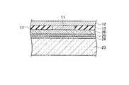
本発明の第1の実施の形態に係る半導体発光素子およびその製造方法に適用されるLEDの模式的断面構造は、図3に示すように、金属層12と、金属層12上に配置される金属コンタクト層11と、金属コンタクト層11上に配置されるp型クラッド層10と、p型クラッド層10上に配置されるMQW層9と、MQW層9上に配置されるn型クラッド層8と、n型クラッド層8上に配置されるウィンドウ層7を備える。 A schematic cross-sectional structure of an LED applied to the semiconductor light emitting device and the method for manufacturing the same according to the first embodiment of the present invention is arranged on a
図3の構造において、金属層12は、例えばAu層で形成される。また、金属コンタクト層は、例えばAuBe層あるいはAuBeとNiとの合金層などで形成される。p型クラッド層10は、例えばAlGaAs層若しくは導電型をp-型とするAlGaAs層と導電型をp+型とするAlGaAs層との多層構造によって形成され、厚さは、例えば約0.1μm程度である。MQW層9は、例えばGaAs/GaAlAs層からなるヘテロ接合ペアを約100ペア積層した多重量子井戸構造からなり、厚さは、例えば約1.6μm程度に形成される。n型クラッド層8は、例えばn型AlGaAs層によって形成され、厚さは、例えば約0.1μm程度である。ウィンドウ層7は、例えばAlGaAs層の多層構造とAlGaAs層の多層構造上に形成されたGaAs層からなり、全体の厚さは、約0.95μm程度である。In the structure of FIG. 3, the
本発明の第1の実施の形態に係る半導体発光素子は、図4に示すように、図1乃至図2に示したp型乃至n型GaAs基板と、図3に示したLED構造をウェハボンディング技術によって互いに貼り付けて形成する。 As shown in FIG. 4, the semiconductor light emitting device according to the first embodiment of the present invention includes a p-type to n-type GaAs substrate shown in FIGS. 1 and 2 and an LED structure shown in FIG. Paste each other by technology.
すなわち、本発明の第1の実施の形態に係る半導体発光素子は、図4に示すように、p(n)型GaAs層3(6)と、p(n)型GaAs層3(6)の表面に配置された金属バッファ層2と、金属バッファ層2上に配置された金属層1と、p(n)型GaAs層3(6)の裏面に配置された金属バッファ層4と、金属バッファ層4のp(n)型GaAs層3(6)と反対側の表面に配置された金属層5とを備えるp(n)型GaAs基板構造と、当該p(n)型GaAs基板上に配置され、金属層12と、金属層12上に配置される金属コンタクト層11と、金属コンタクト層11上に配置されるp型クラッド層10と、p型クラッド層10上に配置されるMQW層9と、MQW層9上に配置されるn型クラッド層8と、n型クラッド層8上に配置されるウィンドウ層7を備えるLED構造とから構成される。 That is, the semiconductor light emitting device according to the first embodiment of the present invention includes a p (n) type GaAs layer 3 (6) and a p (n) type GaAs layer 3 (6) as shown in FIG. A
Au−Sn合金層からのSn拡散の問題点を解決するために、金属層1および金属層12を用いて、p(n)型GaAs基板構造と、エピタキシャル成長層からなるLED構造を貼り付けることにより、バリアメタルが不要で、反射率のよい金属反射層を形成することを可能にしている。金属反射層は、予め、LED構造側に配置された金属層12によって形成される。LEDからの放射光は、p型クラッド層10と、金属層12との界面によってミラー面が形成されるため、当該ミラー面において反射される。金属コンタクト層11は金属層12とp型クラッド層10とのオーミックコンタクトを取るための層であるが、金属層12とp型クラッド層10との界面に介在し、ミラー面の一部を形成している。 In order to solve the problem of Sn diffusion from the Au—Sn alloy layer, the metal layer 1 and the
本発明の第1の実施の形態に係る半導体発光素子は、図4に示すように、金属層1および金属層12をともにAu層によって形成することで、GaAs基板側の金属層1とエピタキシャル成長層からなるLED構造側の金属層12を熱圧着によって貼り付けることができる。 As shown in FIG. 4, the semiconductor light emitting device according to the first embodiment of the present invention is formed by forming both the metal layer 1 and the
貼付けの条件は、例えば、約250℃〜700℃、望ましくは300℃〜400℃であり、熱圧着の圧力は、例えば、約10MPa〜20MPa程度である。 The pasting condition is, for example, about 250 ° C. to 700 ° C., desirably 300 ° C. to 400 ° C., and the pressure of thermocompression bonding is, for example, about 10 MPa to 20 MPa.
本発明の第1の実施の形態に係る半導体発光素子によれば、Auからなる金属層12を用いることで光の反射率の良い金属反射層をLED側の構造に形成することができるので、LEDの高輝度化を図ることができる。 According to the semiconductor light emitting device according to the first embodiment of the present invention, a metal reflective layer with good light reflectivity can be formed in the LED side structure by using the
[第2の実施の形態]
(素子構造)
図5は、本発明の第2の実施の形態に係る半導体発光素子およびその製造方法に適用されるLEDの模式的断面構造を示す。また、図6は、本発明の第2の実施の形態の変形例に係る半導体発光素子およびその製造方法に適用されるLEDの模式的断面構造を示す。[Second Embodiment]
(Element structure)
FIG. 5 shows a schematic cross-sectional structure of an LED applied to the semiconductor light emitting device and the method for manufacturing the same according to the second embodiment of the present invention. FIG. 6 shows a schematic cross-sectional structure of an LED applied to a semiconductor light emitting device and a method for manufacturing the same according to a modification of the second embodiment of the present invention.
図7は、p型乃至n型GaAs基板15と、図6に示したLEDをウェハボンディング技術によって互いに貼り付けて形成した本発明の第2の実施の形態に係る半導体発光素子の模式的断面構造を示す。尚、図7において、GaAs基板15上に配置される、例えばAu層からなる金属層は、図示を省略している。或いはまた、GaAs基板15上にはAu層などの金属層を配置せず、金属層12のみでGaAs基板15とLED構造を貼り付けることも可能である。 FIG. 7 is a schematic cross-sectional structure of a semiconductor light emitting device according to the second embodiment of the present invention formed by bonding the p-type to n-
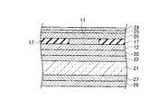
本発明の第2の実施の形態に係る半導体発光素子およびその製造方法に適用されるLEDは、図5に示すように、金属層12と、金属層12上に配置され,パターニングされた金属コンタクト層11および絶縁層17と、パターニングされた金属コンタクト層11および絶縁層17上に配置されるp型クラッド層10と、p型クラッド層10上に配置されるMQW層9と、MQW層9上に配置されるn型クラッド層8と、n型クラッド層8上に配置されるウィンドウ層7を備える。 As shown in FIG. 5, the LED applied to the semiconductor light emitting device and the manufacturing method thereof according to the second embodiment of the present invention has a
図5の構造において、金属層12は、例えばAu層で形成され、例えば厚さは約2.5〜5μm程度である。また、金属コンタクト層11は、例えばAuBe層あるいはAuBeとNiとの合金層などで形成され、例えば厚さは、絶縁層17と同程度であり、約450nm程度である。絶縁層17は、例えばシリコン酸化膜、シリコン窒化膜、SiON膜、SiOxNy膜、或いはこれらの多層膜などで形成される。p型クラッド層10は、例えばAlGaAs層若しくは導電型をp-型とするAlGaAs層と導電型をp+型とするAlGaAs層との多層構造によって形成され、厚さは、例えば約0.1μm程度である。MQW層9は、例えばGaAs/GaAlAs層からなるヘテロ接合ペアを約100ペア積層した多重量子井戸構造からなり、厚さは、例えば約1.6μm程度に形成される。n型クラッド層8は、例えばn型AlGaAs層によって形成され、厚さは、例えば約0.1μm程度である。ウィンドウ層7は、例えばAlGaAs層の多層構造とAlGaAs層の多層構造上に形成されたGaAs層からなり、全体の厚さは、約0.95μm程度である。In the structure of FIG. 5, the
(第2の実施の形態の変形例)
本発明の第2の実施の形態の変形例に係る半導体発光素子およびその製造方法に適用されるLEDは、図6に示すように、金属層12と、金属層12上に配置される金属バッファ層18と、金属バッファ層18上に配置され,パターニングされた金属コンタクト層11および絶縁層17と、パターニングされた金属コンタクト層11および絶縁層17上に配置されるp型クラッド層10と、p型クラッド層10上に配置されるMQW層9と、MQW層9上に配置されるn型クラッド層8と、n型クラッド層8上に配置されるウィンドウ層7を備える。(Modification of the second embodiment)
As shown in FIG. 6, the LED applied to the semiconductor light emitting device and the manufacturing method thereof according to the modification of the second embodiment of the present invention includes a
図6の構造において、金属バッファ層18は、例えばAg、Al、Ni、Cr若しくはW層で形成される。Au層からなる金属層12は青色光、紫外光を吸収するため、このような短波長側の光を反射するためには、Ag、Alなどからなる金属バッファ層18を備えることが望ましい。図6の構造において、金属バッファ層18以外の各層は、図5の構造と同様に形成されるため、説明を省略する。 In the structure of FIG. 6, the
本発明の第2の実施の形態に係る半導体発光素子は、図7に示すように、図5乃至図6に示したLED構造と、GaAs基板15をウェハボンディング技術によって互いに貼り付けて形成する。 As shown in FIG. 7, the semiconductor light emitting device according to the second embodiment of the present invention is formed by bonding the LED structure shown in FIGS. 5 to 6 and the
すなわち、本発明の第2の実施の形態に係る半導体発光素子は、図7に示すように、GaAs基板15と、GaAs基板15上に配置される金属層12と、金属層12上に配置される金属バッファ層18と、金属バッファ層18上に配置され,パターニングされた金属コンタクト層11および絶縁層17と、パターニングされた金属コンタクト層11および絶縁層17上に配置されるp型クラッド層10と、p型クラッド層10上に配置されるMQW層9と、MQW層9上に配置されるn型クラッド層8と、n型クラッド層8上に配置されるウィンドウ層7を備えるLED構造とから構成される。 That is, the semiconductor light emitting device according to the second embodiment of the present invention is disposed on the
金属層12を用いて、GaAs基板15と、エピタキシャル成長層からなるLED構造を貼り付けることにより、反射率のよい金属反射層を形成することを可能にしている。金属反射層は、予め、LED構造側に配置された金属層12によって形成される。LEDからの放射光は、絶縁層17と、金属層12若しくは金属バッファ層18との界面によってミラー面が形成されるため、当該ミラー面において反射される。金属コンタクト層11は、金属層12若しくは金属バッファ層18とp型クラッド層10とのオーミックコンタクトを取るための層であるが、金属層12とp型クラッド層10との界面に介在し、絶縁層17と同程度の厚さを有する。 By using the
金属コンタクト層11のパターン幅が広い場合には、実質的な発光領域が制限されるため、面積効率が低下し発光効率が減少する。一方、金属コンタクト層11のパターン幅が狭い場合には、金属コンタクト層11の面積抵抗が増大し、LEDの順方向電圧Vfが上昇するため、最適なパターン幅およびパターン構造が存在する。幾つかのパターン例では、六角形を基本とするハニカムパターン構造、或いは、円形を基本とするドットパターン構造が存在する。これらのパターン形状については、第4の実施の形態に関連して、図13および図14において説明する。 When the pattern width of the
本発明の第2の実施の形態に係る半導体発光素子は、図4に示すように、GaAs基板上に配置される金属層、およびLED側に配置される金属層12をともにAu層によって形成することで、GaAs基板側の金属層(図示省略)とエピタキシャル成長層からなるLED構造側の金属層12を熱圧着によって貼り付けることができる。 In the semiconductor light emitting device according to the second embodiment of the present invention, as shown in FIG. 4, both the metal layer disposed on the GaAs substrate and the
貼付けの条件は、例えば、約250℃〜700℃、望ましくは300℃〜400℃であり、熱圧着の圧力は、例えば、約10MPa〜20MPa程度である。 The pasting condition is, for example, about 250 ° C. to 700 ° C., desirably 300 ° C. to 400 ° C., and the pressure of thermocompression bonding is, for example, about 10 MPa to 20 MPa.
本発明の第2の実施の形態に係る半導体発光素子によれば、金属反射層となる金属層12若しくは金属バッファ層18と、p型クラッド層10などの半導体層との間に透明な絶縁層17を形成することにより、p型クラッド層10などの半導体層と金属層12との接触を避け、光の吸収を防ぎ、反射率の良い金属反射層を形成することができる。 According to the semiconductor light emitting device according to the second embodiment of the present invention, a transparent insulating layer is provided between the
透明な絶縁層17をパターニング形成し、オーミックをとるために、AuBeなどからなる金属コンタクト層11をリフトオフによって蒸着する。 A transparent insulating
その後、絶縁層17の上にGaAs基板15と貼付けるために用いるAu層を蒸着し、金属層12を形成する。 Thereafter, an Au layer used for adhering to the
本発明の第2の実施の形態に係る半導体発光素子によれば、金属反射層と半導体層との間に透明な絶縁層17を介在させることにより、p型クラッド層10などの半導体層と金属層12との接触を避け、光の吸収を防ぎ、反射率の良い金属反射層を形成することができるので、LEDの高輝度化を図ることができる。 According to the semiconductor light emitting device of the second embodiment of the present invention, the transparent insulating
また、本発明の第2の実施の形態に係る半導体発光素子によれば、絶縁層17と金属層12との間に、AgやAlなどからなる金属バッファ層18を形成することで、Auでは反射率の低い紫外線などの短波長の光を効率よく反射することができ、LEDの高輝度化を図ることができる。 In addition, according to the semiconductor light emitting device according to the second embodiment of the present invention, by forming the
また、本発明の第2の実施の形態に係る半導体発光素子によれば、p型クラッド層と金属反射層の界面において光が吸収されないため、LEDの高輝度化を図ることができる。 Further, according to the semiconductor light emitting device according to the second embodiment of the present invention, light is not absorbed at the interface between the p-type cladding layer and the metal reflection layer, so that the brightness of the LED can be increased.
[第3の実施の形態]
(素子構造)
図8は、本発明の第3の実施の形態に係る半導体発光素子およびその製造方法に適用されるGaAs基板の模式的断面構造を示す。また、図9は、本発明の第3の実施の形態に係る半導体発光素子およびその製造方法に適用されるLEDの模式的断面構造を示す。[Third embodiment]
(Element structure)
FIG. 8 shows a schematic cross-sectional structure of a GaAs substrate applied to the semiconductor light emitting device and the method for manufacturing the same according to the third embodiment of the present invention. FIG. 9 shows a schematic cross-sectional structure of an LED applied to the semiconductor light emitting device and the method for manufacturing the same according to the third embodiment of the present invention.
図10は、図8に示した金属層20を備えるGaAs基板15と、図9に示したLEDをウェハボンディング技術によって互いに貼り付けて形成した本発明の第3の実施の形態に係る半導体発光素子の模式的断面構造を示す。 FIG. 10 shows a semiconductor light emitting device according to the third embodiment of the present invention formed by bonding the
本発明の第3の実施の形態に係る半導体発光素子およびその製造方法に適用されるp型若しくはn型GaAs基板構造は、図8に示すように、GaAs基板15と、GaAs基板15の表面に配置された金属層20を備える。 As shown in FIG. 8, the p-type or n-type GaAs substrate structure applied to the semiconductor light emitting device and the method for manufacturing the same according to the third embodiment of the present invention has a
図8の構造において、金属層20は、例えばAu層によって形成される。 In the structure of FIG. 8, the
本発明の第3の実施の形態に係る半導体発光素子およびその製造方法に適用されるLEDの模式的断面構造は、図9に示すように、金属層12と、金属層12上に配置されるp型クラッド層10と、p型クラッド層10上に配置されるMQW層9と、MQW層9上に配置されるn型クラッド層8と、n型クラッド層8上に配置されるウィンドウ層7を備える。 A schematic cross-sectional structure of an LED applied to a semiconductor light emitting device and a method for manufacturing the same according to a third embodiment of the present invention is arranged on a
図9の構造において、金属層12は、例えばAu層で形成され、厚さは例えば、約1μm程度である。また、p型クラッド層10は、例えばAlGaAs層若しくは導電型をp-型とするAlGaAs層と導電型をp+型とするAlGaAs層との多層構造によって形成され、全体の厚さは、例えば約0.1μm程度に形成される。MQW層9は、例えばGaAs/GaAlAs層からなるヘテロ接合ペアを約80〜100ペア積層した多重量子井戸構造からなり、全体の厚さは、例えば約1.6μm程度に形成される。n型クラッド層8は、例えばn型AlGaAs層によって形成され、厚さは、例えば約0.1μm程度である。ウィンドウ層7は、例えばAlGaAs層の多層構造とAlGaAs層の多層構造上に形成されたGaAs層からなり、全体の全体の厚さは、約0.95μm程度である。In the structure of FIG. 9, the
本発明の第3の実施の形態に係る半導体発光素子は、図10に示すように、図8に示したp型乃至n型GaAs基板と、図9に示したLED構造をウェハボンディング技術によって互いに貼り付けて形成する。 As shown in FIG. 10, the semiconductor light emitting device according to the third embodiment of the present invention has a p-type to n-type GaAs substrate shown in FIG. 8 and the LED structure shown in FIG. Paste to form.
すなわち、本発明の第3の実施の形態に係る半導体発光素子は、図10に示すように、GaAs基板15と、GaAs基板15の表面に配置された金属層20とを備えるGaAs基板構造と、当該GaAs基板構造上に配置され、金属層12と、金属層12上に配置されるp型クラッド層10と、p型クラッド層10上に配置されるMQW層9と、MQW層9上に配置されるn型クラッド層8と、n型クラッド層8上に配置されるウィンドウ層7を備えるLED構造とから構成される。 That is, the semiconductor light-emitting device according to the third embodiment of the present invention includes a GaAs substrate structure including a
金属反射層は、予め、LED構造側に配置された金属層12によって形成される。LEDからの放射光は、p型クラッド層10と、金属層12との界面によってミラー面が形成されるため、当該ミラー面において反射される。 The metal reflection layer is formed in advance by the
本発明の第3の実施の形態に係る半導体発光素子は、図10に示すように、金属層20および金属層12をともにAu層によって形成することで、GaAs基板側の金属層20とエピタキシャル成長層からなるLED構造側の金属層12を熱圧着によって貼り付けることができる。 As shown in FIG. 10, the semiconductor light emitting device according to the third embodiment of the present invention is formed by forming both the
貼付けの条件は、例えば、約250℃〜700℃、望ましくは300℃〜400℃であり、熱圧着の圧力は、例えば、約10MPa〜20MPa程度である。 The pasting condition is, for example, about 250 ° C. to 700 ° C., desirably 300 ° C. to 400 ° C., and the pressure of thermocompression bonding is, for example, about 10 MPa to 20 MPa.
本発明の第3の実施の形態に係る半導体発光素子およびその製造方法によれば、GaAs基板への光の吸収を防ぐために、反射層に金属を用いて光を全反射させ、GaAs基板への吸収を防ぐようにした点に特徴を有する。貼付ける半導体基板の材料としては、GaAs、Siなどの不透明な半導体基板材料を用いる。 According to the semiconductor light emitting device and the manufacturing method thereof according to the third embodiment of the present invention, in order to prevent light absorption to the GaAs substrate, the light is totally reflected using a metal in the reflective layer, It is characterized in that absorption is prevented. As a material of the semiconductor substrate to be pasted, an opaque semiconductor substrate material such as GaAs or Si is used.
GaAs基板15側の金属層20としてAu層を用い、エピタキシャル成長層を備えるLED側の金属層12としてもAu層を用い、金属層20と金属層12を結合させ、結合に用いた金属層12を金属反射層として光の反射層とする。 An Au layer is used as the
本発明の第3の実施の形態に係る半導体発光素子およびその製造方法によれば、GaAs基板への光の吸収を防ぐために、反射層に金属を用いて光を全反射させ、GaAs基板への吸収を防ぎ、あらゆる角度の光を反射することが可能になるので、LEDを高輝度化することができる。 According to the semiconductor light emitting device and the manufacturing method thereof according to the third embodiment of the present invention, in order to prevent light absorption to the GaAs substrate, the light is totally reflected using a metal in the reflective layer, Since it becomes possible to prevent absorption and reflect light at all angles, the LED can be made brighter.
[第4の実施の形態]
(素子構造)
図11は、本発明の第4の実施の形態に係る半導体発光素子およびその製造方法に適用されるシリコン基板の模式的断面構造を示す。また、図12は、本発明の第4の実施の形態に係る半導体発光素子およびその製造方法に適用されるLEDの模式的断面構造を示す。図13は、本発明の第4の実施の形態に係る半導体発光素子およびその製造方法に適用されるLEDの模式的平面パターン構造を示し、図14は、別の模式的平面パターン構造を示す。[Fourth embodiment]
(Element structure)
FIG. 11 shows a schematic cross-sectional structure of a silicon substrate applied to the semiconductor light emitting device and the method for manufacturing the same according to the fourth embodiment of the present invention. FIG. 12 shows a schematic cross-sectional structure of an LED applied to the semiconductor light emitting device and the method for manufacturing the same according to the fourth embodiment of the present invention. FIG. 13 shows a schematic planar pattern structure of an LED applied to the semiconductor light emitting device and the manufacturing method thereof according to the fourth embodiment of the present invention, and FIG. 14 shows another schematic planar pattern structure.
本発明の第4の実施の形態に係る半導体発光素子およびその製造方法に適用されるシリコン基板21は、図11に示すように、シリコン基板21と、シリコン基板21の表面に配置されたチタン(Ti)層22と、チタン(Ti)層22をの表面に配置された金属層20を備える。 As shown in FIG. 11, the
図11の構造において、シリコン基板21の厚さは、例えば約130μm程度であり、金属層20は、例えばAu層によって形成され、厚さは約2.5μm程度である。 In the structure of FIG. 11, the thickness of the
本発明の第4の実施の形態に係る半導体発光素子およびその製造方法に適用されるLEDは、図12に示すように、GaAs基板23と、GaAs基板23上に配置されるAlInGaP層24と、AlInGaP層24上に配置されるn型GaAs層25と、n型GaAs層25上に配置されるエピタキシャル成長層26と、エピタキシャル成長層26上に配置され,パターニングされた金属コンタクト層11および絶縁層17と、パターニングされた金属コンタクト層11および絶縁層17上に配置される金属層12とを備える。 As shown in FIG. 12, the LED applied to the semiconductor light emitting device and the manufacturing method thereof according to the fourth embodiment of the present invention includes a
図12の構造において、GaAs基板23は、厚さは、例えば約300μm程度であり、AlInGaP層24は、厚さは、例えば約350nm程度である。また、n型GaAs層25は、AlInGaP層24を介して、GaAs基板23とエピタキシャル成長層26との間のコンタクト層として働き、厚さは、例えば約500nm程度である。エピタキシャル成長層26は、AlGaAs層からなるn型ウィンドウ層およびn型クラッド層、GaAs/AlGaAsのヘテロ接合の複数の対からなるMQW層と、AlGaAs層からなるn型クラッド層およびAlGaAs層/GaP層からなるp型ウィンドウ層とを備える。MQW層は、例えばGaAs/GaAlAs層からなるヘテロ接合ペアを約100ペア積層した多重量子井戸構造からなり、厚さは、例えば約1.6μm程度に形成される。 In the structure of FIG. 12, the
また、金属コンタクト層11は、例えばAuBe層あるいはAuBeとNiとの合金層などで形成され、例えば厚さは、絶縁層17と同程度であり、約450nm程度である。 The
金属コンタクト層11は、例えばAu/AuBe−Ni合金/Auなどの積層構造として形成してもよい。絶縁層17は、例えばシリコン酸化膜、シリコン窒化膜、SiON膜、SiOxNy膜、或いはこれらの多層膜などで形成される。The
金属層12は、例えばAu層で形成され、例えば厚さは約2.5〜5μm程度である。エピタキシャル成長層26内のp型クラッド層は、例えばAlGaAs層若しくは導電型をp-型とするAlGaAs層と導電型をp+型とするAlGaAs層との多層構造によって形成され、厚さは、例えば約0.1μm程度である。エピタキシャル成長層26内のn型クラッド層は、例えばn型AlGaAs層によって形成され、厚さは、例えば約0.1μm程度である。n型ウィンドウ層は、例えばAlGaAs層の多層構造とAlGaAs層の多層構造上に形成されたGaAs層からなり、全体の厚さは、例えば、約0.95μm程度である。p型ウィンドウ層は、例えばAlGaAs層の多層構造とAlGaAs層の多層構造上に形成されたGaP層からなり、全体の厚さは、例えば、約0.32μm程度である。The
本発明の第4の実施の形態に係る半導体発光素子は、図20に示すように、図11に示したシリコン基板構造と、図12に示したLED構造をウェハボンディング技術によって互いに貼り付けて形成する。 As shown in FIG. 20, the semiconductor light emitting device according to the fourth embodiment of the present invention is formed by bonding the silicon substrate structure shown in FIG. 11 and the LED structure shown in FIG. 12 to each other by wafer bonding technology. To do.
すなわち、本発明の第4の実施の形態に係る半導体発光素子は、図20に示すように、シリコン基板21と、シリコン基板21上に配置されるチタン層22と、チタン層22上に配置される金属層20とから構成されるシリコン基板構造と、金属層20上に配置される金属層12と、金属層12上に配置され,パターニングされた金属コンタクト層11および絶縁層17と、パターニングされた金属コンタクト層11および絶縁層17上に配置され,露出された表面にフロスト処理領域30(露出されたn型GaAs層25をフロスト処理して形成された領域)を有するエピタキシャル成長層26と、エピタキシャル成長層26上に配置され,パターニングされたn型GaAs層25と、n型GaAs層25上に配置され,同様にパターニングされた表面電極層29とから構成されるLED構造を備える。尚、シリコン基板構造において、シリコン基板21の裏面には、チタン層27と、裏面電極層28が配置される。また、エピタキシャル成長層26とn型GaAs層25の間には、後述する図21、図22に示すように、電流集中を防止するための阻止層31を配置しても良い。この場合の阻止層31の材料としては、GaAsを適用することができ、厚さは、例えば約500nm程度である。 That is, the semiconductor light emitting device according to the fourth embodiment of the present invention is disposed on the
本発明の第4の実施の形態に係る半導体発光素子においても、図20に示すように、金属層12を用いて、シリコン基板構造と、エピタキシャル成長層からなるLED構造を貼り付けることにより、反射率のよい金属反射層を形成することを可能にしている。金属反射層は、予め、LED構造側に配置された金属層12によって形成される。LEDからの放射光は、絶縁層17と金属層12との界面によってミラー面が形成されるため、当該ミラー面において反射される。金属コンタクト層11は、金属層12とエピタキシャル成長層26とのオーミックコンタクトを取るための層であるが、金属層12とエピタキシャル成長層26との界面に介在し、絶縁層17と同程度の厚さを有する。 Also in the semiconductor light emitting device according to the fourth embodiment of the present invention, as shown in FIG. 20, by using a
(平面パターン構造)
金属コンタクト層11のパターン幅が広い場合には、実質的な発光領域が制限されるため、面積効率が低下し発光効率が減少する。一方、金属コンタクト層11のパターン幅が狭い場合には、金属コンタクト層11の面積抵抗が増大し、LEDの順方向電圧Vfが上昇する。このため、最適なパターン幅WおよびパターンピッチD1が存在する。幾つかのパターン例では、六角形を基本とするハニカムパターン構造、或いは、円形ドット形状を基本構造とする円形ドットパターン構造が存在する。(Plane pattern structure)
When the pattern width of the
本発明の第4の実施の形態に係る半導体発光素子およびその製造方法に適用されるLEDの模式的平面パターン構造は、例えば図13に示すように、六角形を基本構造とするハニカムパターン構造を有する。図13において、幅Wで示される形状部分が図12における例えばAuBe層あるいはAuBeとNiとの合金層などで形成される金属コンタクト層11のパターンを示し、幅D1を有する六角形パターンは、絶縁層17の部分に相当し、LEDからの放射光が導光する領域を表す。幅D1は、例えば約100μm程度であり、線幅Wは、約5μm〜約11μm程度である。 The schematic planar pattern structure of the LED applied to the semiconductor light emitting device and the manufacturing method thereof according to the fourth embodiment of the present invention is a honeycomb pattern structure having a hexagonal basic structure as shown in FIG. Have. In FIG. 13, the shape portion indicated by the width W indicates the pattern of the
本発明の第4の実施の形態に係る半導体発光素子およびその製造方法に適用されるLEDの別の模式的平面パターン構造は、例えば図14に示すように、円形を基本とするドットパターン構造を有する。図14において、幅dで示される形状部分が図12における例えばAuBe層あるいはAuBeとNiとの合金層などで形成される金属コンタクト層11のパターンを示し、幅D2を有するパターンピッチで配置されている。図14において、幅d、パターンピッチD2を有する円形のパターン部分以外の領域が、絶縁層17の部分に相当し、LEDからの放射光が導光する領域を表す。パターンピッチD2は、例えば約100μm程度であり、幅dは、約5μm〜約11μm程度である。 Another schematic planar pattern structure of the LED applied to the semiconductor light emitting element and the manufacturing method thereof according to the fourth embodiment of the present invention is a dot pattern structure based on a circle, for example, as shown in FIG. Have. 14, the shape portion indicated by the width d indicates the pattern of the
また、本発明の第4の実施の形態に係る半導体発光素子およびその製造方法に適用されるLEDの模式的平面パターン構造は、六角形ハニカムパターン、円形ドットパターンに限定されるものではなく、三角形パターン、矩形パターン、六角形パターン、八角形パターン、円形ドットパターンなどをランダムに配置するランダムパターンを適用することもできる。 In addition, the schematic planar pattern structure of the LED applied to the semiconductor light emitting device and the manufacturing method thereof according to the fourth embodiment of the present invention is not limited to the hexagonal honeycomb pattern and the circular dot pattern, but a triangle. A random pattern in which a pattern, a rectangular pattern, a hexagonal pattern, an octagonal pattern, a circular dot pattern, etc. are randomly arranged can also be applied.
本発明の第4の実施の形態に係る半導体発光素子に適用されるLEDの模式的平面パターン構造は、導光領域の面積を確保してLEDからの発光輝度を低下させず、かつをLEDの順方向電圧Vfが上昇しない程度の金属配線パターン幅を確保できればよい。 The schematic planar pattern structure of the LED applied to the semiconductor light emitting device according to the fourth embodiment of the present invention secures the area of the light guide region and does not decrease the light emission luminance from the LED. It is only necessary to secure a metal wiring pattern width that does not increase the forward voltage Vf.
(製造方法)
本発明の第4の実施の形態に係る半導体発光素子の製造方法を以下に説明する。(Production method)
A method for manufacturing a semiconductor light emitting element according to the fourth embodiment of the present invention will be described below.
図11乃至図20は、本発明の第4の実施の形態に係る半導体発光素子の製造方法の一工程を説明する模式的断面構造を示す。 11 to 20 show a schematic cross-sectional structure for explaining one process of the method for manufacturing the semiconductor light emitting device according to the fourth embodiment of the present invention.
(a)まず、図11に示すように、貼付け用のシリコン基板構造、および図12に示すように、貼付け用のLED構造を準備する。(A) First, as shown in FIG. 11, a silicon substrate structure for pasting and an LED structure for pasting as shown in FIG. 12 are prepared.
シリコン基板構造においては、シリコン基板21上にチタン層22およびAuなどからなる金属層20をスパッタリング法、真空蒸着法などを用いて順次形成する。 In the silicon substrate structure, a
LED構造においては、GaAs基板23上のAlInGaP層24、n型GaAs層25、エピタキシャル成長層26は、分子線エピタキシャル成長法(MBE:Molecular Beam Epitaxy)、MOCVD(Metal Organic Chemical Vapor Deposition)法などを用いて順次形成する。次に、エピタキシャル成長層26上にリフトオフ法を用いて、パターニングされた絶縁層17に対して、金属コンタクト層11および金属層12を形成する。 In the LED structure, the
(b)次に、図15に示すように、図11に示す貼付け用のシリコン基板構造、および図12に示す貼付け用のLED構造を貼り付ける。貼り付け工程においては、例えばプレス機を用いて、熱圧着温度として約340℃程度、熱圧着の圧力として約18MPa程度、熱圧着の時間として約10分程度の条件で実施する。(B) Next, as shown in FIG. 15, the silicon substrate structure for pasting shown in FIG. 11 and the LED structure for pasting shown in FIG. 12 are pasted. In the attaching step, for example, using a press machine, the thermocompression bonding temperature is about 340 ° C., the thermocompression bonding pressure is about 18 MPa, and the thermocompression bonding time is about 10 minutes.
(c)次に、図16に示すように、シリコン基板21の裏面に対して、チタン層27およびAuなどからなる裏面電極層28をスパッタリング法、真空蒸着法などを用いて順次形成する。チタン層27をAu層とシリコン基板21との間に介在させない場合、オーミックコンタクトをとるためにシンタリングを実施するとシリコン基板21とAu層との接合部のAuがAuSiシリサイドとなり反射率が低下する。したがって、チタン層27は、シリコン基板21とAu層との接着用の金属である。AuSiシリサイド化を防ぐためには、バリアメタルとしてタングステン(W)が必要であり、そのときの構造として、基板側から、シリコン基板/Ti/W/Auで金属層を形成する必要がある。(C) Next, as shown in FIG. 16, a
(d)次に、図17に示すように、裏面電極層28をレジストなどで保護した後、GaAs基板23をエッチングにより除去する。例えばアンモニア/過酸化水素水からなるエッチング液を用い、エッチング時間は、約65〜85分程度である。ここで、AlInGaP層24がエッチングストッパとして重要な働きをする。(D) Next, as shown in FIG. 17, after the
(e)次に、図18に示すように、塩酸系のエッチング液を用いて、AlInGaP層24を除去する。エッチング時間は、例えば約1分半程度である。(E) Next, as shown in FIG. 18, the
(f)次に、図19に示すように、表面電極層29をスパッタリング法、真空蒸着法などを用いて形成後、パターニングする。表面電極層29のパターンは金属コンタクト層11のパターンに略一致させている。表面電極層29の材料としては、例えばAu/AuGe−Ni合金/Auからなる積層構造を用いることができる。ここで、n型GaAs層25は表面電極層29の剥がれ防止機能を有する。(F) Next, as shown in FIG. 19, the
(g)次に、図20に示すように、フロスト処理を実施して、表面電極層29の直下のn型GaAs層25以外のn型GaAs層25の除去を行う。フロスト処理の条件としては、例えば硝酸―硫酸系のエッチング液を約30℃〜50℃,時間約5sec〜15sec程度で行なうことができる。尚、フロスト処理の前処理としては、フッ酸の薄い液を用いてn型GaAs層25をエッチングして、表面に形成されたGaO2膜を除去することができる。エッチング時間としては、例えば約3分程度である。(G) Next, as shown in FIG. 20, a frost process is performed to remove the n-
尚、チタン層22およびチタン層27の代りとして、例えばタングステン(W)バリアメタル、白金(Pt)バリアメタルなどを用いることもできる。 In place of the
以上の説明により、 図20に示すように、シリコン基板21を用いた本発明の第4の実施の形態に係る半導体発光素子が完成される。 As described above, as shown in FIG. 20, the semiconductor light emitting device according to the fourth embodiment of the present invention using the
(第4の実施の形態の変形例)
図21は、本発明の第4の実施の形態の変形例に係る半導体発光素子の製造方法の一工程を説明する模式的断面構造を示す。また、図22は、本発明の第4の実施の形態の別の変形例に係る半導体発光素子の製造方法の一工程を説明する模式的断面構造を示す。(Modification of the fourth embodiment)
FIG. 21 shows a schematic cross-sectional structure for explaining one step of a method for manufacturing a semiconductor light emitting device according to a modification of the fourth embodiment of the present invention. FIG. 22 shows a schematic cross-sectional structure for explaining one process of a method for manufacturing a semiconductor light emitting element according to another modification of the fourth embodiment of the present invention.
本発明の第4の実施の形態の変形例に係る半導体発光素子は、図21に示すように、図11に示したシリコン基板構造と、図12に示したLED構造をウェハボンディング技術によって互いに貼り付けて形成する。 As shown in FIG. 21, the semiconductor light emitting device according to the modification of the fourth embodiment of the present invention is bonded to the silicon substrate structure shown in FIG. 11 and the LED structure shown in FIG. Add and form.
すなわち、本発明の第4の実施の形態に係る半導体発光素子は、図20に示すように、GaAs基板15と、GaAs基板15上に配置される金属バッファ層(AuGe−Ni合金層)32と、金属バッファ層32上に配置される金属層(Au層)33とから構成されるGaAs基板構造と、金属層33上に配置される金属層12と、金属層12上に配置され,パターニングされた金属コンタクト層11および絶縁層17と、パターニングされた金属コンタクト層11および絶縁層17上に配置され,露出された表面にフロスト処理領域30(露出されたn型GaAs層25をフロスト処理して形成された領域)を有するエピタキシャル成長層26と、エピタキシャル成長層26上に配置され,パターニングされたn型GaAs層25と、n型GaAs層25上に配置され,同様にパターニングされた表面電極層29とから構成されるLED構造を備える。尚、GaAs基板構造において、GaAs基板15の裏面には、金属バッファ層(AuGe−Ni合金層)34と、裏面電極層35が配置される。また、エピタキシャル成長層26とn型GaAs層25の間には、図22に示すように、電流集中を防止するための阻止層31を配置しても良い。この場合の阻止層31の材料としては、GaAsを適用することができ、厚さは、例えば約500nm程度である。 That is, the semiconductor light emitting device according to the fourth embodiment of the present invention includes a
本発明の第4の実施の形態の変形例に係る半導体発光素子においても、図21に示すように、金属層12を用いて、GaAs基板構造と、エピタキシャル成長層からなるLED構造を貼り付けることにより、反射率のよい金属反射層を形成することを可能にしている。金属反射層は、予め、LED構造側に配置された金属層12によって形成される。LEDからの放射光は、絶縁層17と金属層12との界面によってミラー面が形成されるため、当該ミラー面において反射される。金属コンタクト層11は、金属層12とエピタキシャル成長層26とのオーミックコンタクトを取るための層であるが、金属層12とエピタキシャル成長層26との界面に介在し、絶縁層17と同程度の厚さを有する。 Also in the semiconductor light emitting device according to the modification of the fourth embodiment of the present invention, as shown in FIG. 21, by using the
図21および図22の構造において、GaAs基板15の裏面に形成される金属バッファ層34は、例えばAuGe−Ni合金層で形成され、厚さは約100nm程度である。また、裏面電極層35は、Au層で形成され、厚さは約500nm程度である。GaAs基板15の表面に形成される金属バッファ層32は、例えばAuGe−Ni合金層で形成され、厚さは約100nm程度である。さらに金属層33は、Au層で形成され、厚さは約1μm程度である。 21 and FIG. 22, the
図11乃至図20に示された本発明の第4の実施の形態に係る半導体発光素子の製造方法の各工程は、本発明の第4の実施の形態の変形例に係る半導体発光素子の製造方法においても同様であるため説明を省略する。 Each process of the manufacturing method of the semiconductor light emitting device according to the fourth embodiment of the present invention shown in FIGS. 11 to 20 includes the steps of manufacturing the semiconductor light emitting device according to the modification of the fourth embodiment of the present invention. Since the method is the same, the description thereof is omitted.
本発明の第4の実施の形態の変形例に係る半導体発光素子およびその製造方法に適用されるLEDの模式的平面パターン構造も、図13或いは図14と同様の構造を適用可能である。 The schematic planar pattern structure of the LED applied to the semiconductor light emitting device and the method for manufacturing the same according to the modification of the fourth embodiment of the present invention can also be applied to the same structure as FIG. 13 or FIG.
また、本発明の第4の実施の形態およびその変形例に係る半導体発光素子においても第2の実施の形態の変形例において説明した、絶縁層17と金属層12との間に、AgやAlなどからなる金属バッファ層18(図6参照)を形成することも有効である。AgやAlなどからなる金属バッファ層18を形成することことで、Auでは反射率の低い紫外線などの短波長の光を効率よく反射することができるからである。 Further, in the semiconductor light emitting device according to the fourth embodiment of the present invention and the modification thereof, Ag or Al is interposed between the insulating
本発明の第4の実施の形態およびその変形例に係る半導体発光素子およびその製造方法によれば、金属反射層と半導体層との間に透明な絶縁層17を介在させることにより、エピタキシャル成長層26と金属層12との接触を避け、光の吸収を防ぎ、反射率の良い金属反射層を形成することができるので、LEDの高輝度化を図ることができる。 According to the semiconductor light emitting device and the manufacturing method thereof according to the fourth embodiment of the present invention and the modification thereof, the
また、本発明の第4の実施の形態およびその変形例に係る半導体発光素子およびその製造方法によれば、絶縁層17と金属層12,20との間に、AgやAlなどからなる金属バッファ層を形成することで、Auでは反射率の低い紫外線などの短波長の光を効率よく反射することができ、LEDの高輝度化を図ることができる。 In addition, according to the semiconductor light emitting device and the manufacturing method thereof according to the fourth embodiment of the present invention and the modification thereof, the metal buffer made of Ag, Al, or the like between the insulating
また、本発明の第4の実施の形態およびその変形例に係る半導体発光素子およびその製造方法によれば、エピタキシャル成長層26と金属層12との接触を避け、エピタキシャル成長層26と金属反射層の界面において光が吸収されないため、LEDの高輝度化を図ることができる。 Further, according to the semiconductor light emitting device and the manufacturing method thereof according to the fourth embodiment of the present invention and the modification thereof, the contact between the
本発明の第4の実施の形態およびその変形例に係る半導体発光素子およびその製造方法によれば、シリコン基板若しくはGaAs基板への光の吸収を防ぐために、反射層に金属を用いて光を全反射させ、シリコン基板若しくはGaAs基板への吸収を防ぎ、あらゆる角度の光を反射することが可能になるので、LEDを高輝度化することができる。 According to the semiconductor light emitting device and the method for manufacturing the same according to the fourth embodiment of the present invention and the modification thereof, the reflection layer is made of metal to prevent light from being absorbed into the silicon substrate or the GaAs substrate. The light can be reflected to prevent absorption into the silicon substrate or the GaAs substrate, and light at any angle can be reflected, so that the brightness of the LED can be increased.
[その他の実施の形態]
上記のように、本発明は第1乃至第4の実施の形態によって記載したが、この開示の一部をなす論述および図面はこの発明を限定するものであると理解すべきではない。この開示から当業者には様々な代替実施の形態、実施例および運用技術が明らかとなろう。[Other embodiments]
As described above, the present invention has been described according to the first to fourth embodiments. However, it should not be understood that the description and drawings constituting a part of this disclosure limit the present invention. From this disclosure, various alternative embodiments, examples and operational techniques will be apparent to those skilled in the art.
本発明の第1乃至第4の実施の形態に係る半導体発光素子およびその製造方法においては、半導体基板として主としてシリコン基板、GaAs基板を例に説明したが、Ge、SiGe、SiC、GaN基板、或いはSiC上のGaNエピタキシャル基板なども充分に利用可能である。 In the semiconductor light emitting device and the manufacturing method thereof according to the first to fourth embodiments of the present invention, the silicon substrate and the GaAs substrate are mainly described as examples of the semiconductor substrate. However, the Ge, SiGe, SiC, GaN substrate, or A GaN epitaxial substrate on SiC or the like can be sufficiently used.
本発明の第1乃至第4の実施の形態に係る半導体発光素子として、主としてLEDを例に説明したが、レーザダイオード(LD:Laser Diode)を構成してもよく、その場合には、分布帰還型(DFB:Distributed Feedback)LD、分布ブラッグ反射型(DBR)LD、面発光LDなどを構成しても良い。 As the semiconductor light emitting device according to the first to fourth embodiments of the present invention, description has been made mainly using the LED as an example. However, a laser diode (LD) may be configured, and in that case, distributed feedback is possible. A DFB (Distributed Feedback) LD, a distributed Bragg reflection type (DBR) LD, a surface emitting LD, or the like may be configured.
このように、本発明はここでは記載していない様々な実施の形態などを含むことは勿論である。したがって、本発明の技術的範囲は上記の説明から妥当な特許請求の範囲に係る発明特定事項によってのみ定められるものである。 As described above, the present invention naturally includes various embodiments that are not described herein. Therefore, the technical scope of the present invention is defined only by the invention specifying matters according to the scope of claims reasonable from the above description.
本発明の実施の形態に係る半導体発光素子およびその製造方法は、GaAs基板、Si基板等の不透明基板を有するLED素子,LD素子等の半導体発光素子全般に利用可能である。 The semiconductor light emitting device and the method for manufacturing the same according to the embodiment of the present invention can be used for general semiconductor light emitting devices such as LED devices and LD devices having an opaque substrate such as a GaAs substrate and a Si substrate.
1、5、12、20、33…金属層(Au層)
2、4、18…金属バッファ層
3…p型GaAs層
6…n型GaAs層
7…ウィンドウ層
8…n型クラッド層
9…多重量子井戸(MQW)層
10…p型クラッド層
11…金属コンタクト層(AuBe−Ni合金)
15、23…GaAs基板
17…絶縁層
21…シリコン(Si)基板
22、27…チタン(Ti)層
24…AlInGaP層
25…n型GaAs層
26…エピタキシャル成長層
29…表面電極層
30…フロスト処理領域
31…阻止層
32、34…金属バッファ層(AuGe−Ni合金)
28、35…裏面電極層1, 5, 12, 20, 33 ... metal layer (Au layer)
2, 4, 18 ...
DESCRIPTION OF
28, 35 ... back electrode layer
Claims (40)
Translated fromJapanese前記GaAs基板構造上に配置され、前記第3金属層上に配置される金属コンタクト層と、前記金属コンタクト層上に配置されるp型クラッド層と、前記p型クラッド層に配置される多重量子井戸層と、前記多重量子井戸層上に配置されるn型クラッド層と、前記n型クラッド層上に配置されるウィンドウ層を備える発光ダイオード構造とから構成され、
前記第1金属層および前記第3金属層は、いずれもAu層で形成され、前記第1金属層および前記第3金属層を用いて、前記GaAs基板構造と、前記発光ダイオード構造を貼り付け、
前記発光ダイオード構造は、前記第3金属層と前記p型クラッド層との間に、前記金属コンタクト層と略同じ厚みであって、パターニングされた開口部を有する絶縁層を含み、前記絶縁層の前記開口部に前記金属コンタクト層が形成されており、前記金属コンタクト層は、Auを含む金属からなり、
前記多重量子井戸層は、GaAs/GaAlAs層からなるヘテロ接合ペアを積層した多重量子井戸構造からなり、前記絶縁層は、前記多重量子井戸層からの発光波長に対して透明であることを特徴とする半導体発光素子。A GaAs layer; a first metal buffer layer disposed on a surface of the GaAs layer; a first metal layer disposed on the first metal buffer layer; and a second metal buffer disposed on a back surface of the GaAs layer. A GaAs substrate structure comprising: a layer; and a second metal layer disposed on a surface of the second metal buffer layer opposite to the GaAs layer;
A metal contact layer disposed on the GaAs substrate structure and disposed on the third metal layer, a p-type cladding layer disposed on the metal contact layer, and a multiple quantum disposed on the p-type cladding layer A light emitting diode structure comprising a well layer, an n-type cladding layer disposed on the multiple quantum well layer, and a window layer disposed on the n-type cladding layer;
The first metal layer and the third metal layer are both formed of an Au layer, and the GaAs substrate structure and the light emitting diode structure are pasted using the first metal layer and the third metal layer,
The light emitting diode structure includes an insulating layer between the third metal layer and the p-type cladding layer, having an approximately same thickness as the metal contact layer and having a patterned opening, The metal contact layer is formed in the opening, and the metal contact layer is made of a metal containing Au,
The multiple quantum well layer has a multiple quantum well structure in which heterojunction pairs made of GaAs / GaAlAs layers are stacked, and the insulating layer is transparent to the emission wavelength from the multiple quantum well layer. A semiconductor light emitting device.
前記GaAs基板上に配置される金属層と、
前記金属層上に配置され,パターニングされた金属コンタクト層および絶縁層と、
パターニングされた前記金属コンタクト層および前記絶縁層上に配置されるp型クラッド層10と、
前記p型クラッド層上に配置される多重量子井戸層と、
前記多重量子井戸層上に配置されるn型クラッド層と、
前記n型クラッド層上に配置されるウィンドウ層を備える発光ダイオード構造とから構成され、
前記金属層を用いて、前記GaAs基板と、前記発光ダイオード構造を貼り付け、
前記金属コンタクト層は、所定のパターン構造が所定の間隔で配置されており、前記金属コンタクト層のパターン幅は5μm〜11μmであり、
前記絶縁層は、前記金属コンタクト層と略同じ厚みであって、パターニングされた開口部を有し、前記絶縁層の前記開口部に前記金属コンタクト層が形成されており、前記金属コンタクト層は、Auを含む金属からなり、
前記多重量子井戸層は、GaAs/GaAlAs層からなるヘテロ接合ペアを積層した多重量子井戸構造からなり、前記絶縁層は、前記多重量子井戸層からの発光波長に対して透明であることを特徴とする半導
ことを特徴とする半導体発光素子。A GaAs substrate;
A metal layer disposed on the GaAs substrate;
A metal contact layer and an insulating layer disposed on and patterned on the metal layer;
A p-type cladding layer 10 disposed on the patterned metal contact layer and the insulating layer;
A multiple quantum well layer disposed on the p-type cladding layer;
An n-type cladding layer disposed on the multiple quantum well layer;
A light emitting diode structure comprising a window layer disposed on the n-type cladding layer,
Using the metal layer, the GaAs substrate and the light emitting diode structure are attached,
The metal contact layer is a predetermined pattern structure are arranged at predetermined intervals, the pattern width of the metal contact layerRi 5μm~11μmder,
The insulating layer has substantially the same thickness as the metal contact layer, has a patterned opening, and the metal contact layer is formed in the opening of the insulating layer. Made of metal containing Au,
The multiple quantum well layer has a multiple quantum well structure in which heterojunction pairs made of GaAs / GaAlAs layers are stacked, and the insulating layer is transparent to the emission wavelength from the multiple quantum well layer. A semiconductor light emitting device characterized in that the semiconductor light emitting device.
当該GaAs基板構造上に配置され、第2金属層と、前記第2金属層上に配置されるp型クラッド層と、前記p型クラッド層上に配置される多重量子井戸層と、前記多重量子井戸層上に配置されるn型クラッド層と、前記n型クラッド層上に配置されるウィンドウ層を備える発光ダイオード構造とから構成され、
前記第1金属層および前記第2金属層は、いずれもAu層で形成され、前記第1金属層および前記第2金属層を用いて、前記GaAs基板と、前記発光ダイオード構造を貼り付け、
前記発光ダイオード構造は、前記第2金属層と前記p型クラッド層との間に、前記金属コンタクト層と略同じ厚みであって、パターニングされた開口部を有する絶縁層を含み、前記絶縁層の前記開口部に前記金属コンタクト層が形成されており、前記金属コンタクト層は、Auを含む金属からなり、
前記多重量子井戸層は、GaAs/GaAlAs層からなるヘテロ接合ペアを積層した多重量子井戸構造からなり、前記絶縁層は、前記多重量子井戸層からの発光波長に対して透明であることを特徴とする半導体発光素子。A GaAs substrate structure comprising a GaAs substrate and a first metal layer disposed on a surface of the GaAs substrate;
A second metal layer disposed on the GaAs substrate structure; a p-type cladding layer disposed on the second metal layer; a multiple quantum well layer disposed on the p-type cladding layer; and the multiple quantum An n-type cladding layer disposed on the well layer, and a light emitting diode structure including a window layer disposed on the n-type cladding layer,
The first metal layer and the second metal layer are both formed of an Au layer, and the GaAs substrate and the light emitting diode structure are attached using the first metal layer and the second metal layer,
The light emitting diode structure includes an insulating layer between the second metal layer and the p-type cladding layer, having an approximately same thickness as the metal contact layer and having a patterned opening, The metal contact layer is formed in the opening, and the metal contact layer is made of a metal containing Au,
The multiple quantum well layer has a multiple quantum well structure in which heterojunction pairs made of GaAs / GaAlAs layers are stacked, and the insulating layer is transparent to the emission wavelength from the multiple quantum well layer. A semiconductor light emitting device.
前記第1金属層上に配置される第2金属層と、前記第2金属層上に配置され,パターニングされた金属コンタクト層および絶縁層と、パターニングされた前記金属コンタクト層および前記絶縁層上に配置され,露出された表面にフロスト処理領域を有するエピタキシャル成長層と、前記エピタキシャル成長層上に配置され,パターニングされたn型GaAs層と、前記n型GaAs層上に配置され,パターニングされた表面電極層とから構成されるLED構造とを備え、
前記第1金属層および前記第2金属層を用いて、前記シリコン基板構造と、前記発光ダイオード構造を貼り付け、
前記金属コンタクト層は、所定のパターン構造が所定の間隔で配置されており、前記金属コンタクト層のパターン幅は5μm〜11μmであり、
前記絶縁層は、前記金属コンタクト層と略同じ厚みであって、パターニングされた開口部を有し、前記絶縁層の前記開口部に前記金属コンタクト層が形成されており、前記金属コンタクト層は、Auを含む金属からなり、
前記エピタキシャル成長層は、GaAs/GaAlAs層からなるヘテロ接合ペアを積層した多重量子井戸構造からなる多重量子井戸層を含み、前記絶縁層は、前記多重量子井戸層からの発光波長に対して透明であることを特徴とする半導体発光素子。A silicon substrate structure composed of a silicon substrate, a first titanium layer disposed on the silicon substrate, and a first metal layer disposed on the first titanium layer;
A second metal layer disposed on the first metal layer; a patterned metal contact layer and insulating layer disposed on the second metal layer; and the patterned metal contact layer and insulating layer. An epitaxially grown layer having a frosted region disposed on the exposed surface, an n-type GaAs layer disposed on the epitaxially grown layer and patterned, and a surface electrode layer disposed on the n-type GaAs layer and patterned An LED structure composed of
Using the first metal layer and the second metal layer, the silicon substrate structure and the light emitting diode structure are pasted,
The metal contact layer is a predetermined pattern structure are arranged at predetermined intervals, the pattern width of the metal contact layerRi 5μm~11μmder,
The insulating layer has substantially the same thickness as the metal contact layer, has a patterned opening, and the metal contact layer is formed in the opening of the insulating layer. Made of metal containing Au,
The epitaxially grown layer includes a multiple quantum well layer having a multiple quantum well structure in which heterojunction pairs made of GaAs / GaAlAs layers are stacked, and the insulating layer is transparent to an emission wavelength from the multiple quantum well layer. A semiconductor light emitting element characterized by the above.
前記第1金属層上に配置される第2金属層と、前記第2金属層上に配置され,パターニングされた金属コンタクト層および絶縁層と、パターニングされた前記金属コンタクト層および前記絶縁層上に配置され,露出された表面にフロスト処理領域を有するエピタキシャル成長層と、前記エピタキシャル成長層上に配置され,パターニングされたn型GaAs層と、前記n型GaAs層上に配置され,パターニングされた表面電極層とから構成されるLED構造を備え、
前記第1金属層および前記第2金属層を用いて、前記GaAs基板構造と、前記発光ダイオード構造を貼り付け、
前記金属コンタクト層は、所定のパターン構造が所定の間隔で配置されており、前記金属コンタクト層のパターン幅は5μm〜11μmであり、
前記絶縁層は、前記金属コンタクト層と略同じ厚みであって、パターニングされた開口部を有し、前記絶縁層の前記開口部に前記金属コンタクト層が形成されており、前記金属コンタクト層は、Auを含む金属からなり、
前記エピタキシャル成長層は、GaAs/GaAlAs層からなるヘテロ接合ペアを積層した多重量子井戸構造からなる多重量子井戸層を含み、前記絶縁層は、前記多重量子井戸層からの発光波長に対して透明であることを特徴とする半導体発光素子。A GaAs substrate structure comprising a GaAs substrate, a metal buffer layer disposed on the GaAs substrate, and a first metal layer disposed on the metal buffer layer;
A second metal layer disposed on the first metal layer; a patterned metal contact layer and insulating layer disposed on the second metal layer; and the patterned metal contact layer and insulating layer. An epitaxially grown layer having a frosted region disposed on the exposed surface, an n-type GaAs layer disposed on the epitaxially grown layer and patterned, and a surface electrode layer disposed on the n-type GaAs layer and patterned LED structure composed of
Using the first metal layer and the second metal layer, the GaAs substrate structure and the light emitting diode structure are pasted,
The metal contact layer is a predetermined pattern structure are arranged at predetermined intervals, the pattern width of the metal contact layerRi 5μm~11μmder,
The insulating layer has substantially the same thickness as the metal contact layer, has a patterned opening, and the metal contact layer is formed in the opening of the insulating layer. Made of metal containing Au,
The epitaxially grown layer includes a multiple quantum well layer having a multiple quantum well structure in which heterojunction pairs made of GaAs / GaAlAs layers are stacked, and the insulating layer is transparent to an emission wavelength from the multiple quantum well layer. A semiconductor light emitting element characterized by the above.
半導体基板構造においては、半導体基板上に第1金属層を形成する工程と、
発光ダイオード構造においては、GaAs基板上のAlInGaP層、n型GaAs層、エピタキシャル成長層を順次形成する工程と、
前記エピタキシャル成長層上に、パターニングされた絶縁層に対して、金属コンタクト層および第2金属層を形成する工程と、
前記貼付け用の半導体基板構造、および前記貼付け用のLED構造を熱圧着により貼り付ける工程と、
前記GaAs基板をエッチングにより除去する工程と、
前記AlInGaP層を除去する工程と、
表面電極層をパターン形成する工程と、
フロスト処理を実施して、表面電極層の直下のn型GaAs層以外のn型GaAs層の除去を行う工程と
を有し、
前記金属コンタクト層は、所定のパターン構造が所定の間隔で配置されており、前記金属コンタクト層のパターン幅は5μm〜11μmであり、
前記絶縁層は、前記金属コンタクト層と略同じ厚みであって、パターニングされた開口部を有し、前記絶縁層の前記開口部に前記金属コンタクト層が形成されており、前記金属コンタクト層は、Auを含む金属からなり、
前記エピタキシャル成長層は、GaAs/GaAlAs層からなるヘテロ接合ペアを積層した多重量子井戸構造からなる多重量子井戸層を含み、前記絶縁層は、前記多重量子井戸層からの発光波長に対して透明であることを特徴とする半導体発光素子の製造方法。Preparing a semiconductor substrate structure for pasting and a light emitting diode structure for pasting;
In the semiconductor substrate structure, forming a first metal layer on the semiconductor substrate;
In the light emitting diode structure, a step of sequentially forming an AlInGaP layer, an n-type GaAs layer, and an epitaxial growth layer on a GaAs substrate;
Forming a metal contact layer and a second metal layer on the epitaxially grown layer with respect to the patterned insulating layer;
The step of attaching the semiconductor substrate structure for pasting and the LED structure for pasting by thermocompression bonding,
Removing the GaAs substrate by etching;
Removing theAlInGaP layer ;
Patterning the surface electrode layer;
Performing a frost treatment to remove an n-type GaAs layer other than the n-type GaAs layer directly under the surface electrode layer,
The metal contact layer is a predetermined pattern structure are arranged at predetermined intervals, the pattern width of the metal contact layerRi 5μm~11μmder,
The insulating layer has substantially the same thickness as the metal contact layer, has a patterned opening, and the metal contact layer is formed in the opening of the insulating layer. Made of metal containing Au,
The epitaxially grown layer includes a multiple quantum well layer having a multiple quantum well structure in which heterojunction pairs made of GaAs / GaAlAs layers are stacked, and the insulating layer is transparent to an emission wavelength from the multiple quantum well layer. A method for manufacturing a semiconductor light emitting device.
Priority Applications (17)
| Application Number | Priority Date | Filing Date | Title |
|---|---|---|---|
| JP2007107130AJP5346443B2 (en) | 2007-04-16 | 2007-04-16 | Semiconductor light emitting device and manufacturing method thereof |
| CN201410587684.XACN104409588B (en) | 2007-04-16 | 2008-04-11 | Semiconductor light-emitting elements |
| PCT/JP2008/057176WO2008129963A1 (en) | 2007-04-16 | 2008-04-11 | Semiconductor light-emitting device and method for manufacturing the same |
| US12/596,004US8106412B2 (en) | 2007-04-16 | 2008-04-11 | Semiconductor light emitting device and fabrication method for the same |
| KR1020097023683AKR101446370B1 (en) | 2007-04-16 | 2008-04-11 | Semiconductor light emitting device and manufacturing method thereof |
| CN200880012118ACN101657912A (en) | 2007-04-16 | 2008-04-11 | Semiconductor light emitting element and method for manufacturing the same |
| EP08740273.1AEP2139052B1 (en) | 2007-04-16 | 2008-04-11 | Semiconductor light-emitting device and method for manufacturing the same |
| TW097113675ATWI481065B (en) | 2007-04-16 | 2008-04-15 | Semiconductor light emitting element and manufacturing method thereof |
| US13/327,860US8536598B2 (en) | 2007-04-16 | 2011-12-16 | Semiconductor light emitting device and fabrication method for the same |
| US14/024,696US9018650B2 (en) | 2007-04-16 | 2013-09-12 | Semiconductor light emitting device |
| US14/286,696US9196808B2 (en) | 2007-04-16 | 2014-05-23 | Semiconductor light emitting device |
| US14/928,349US9450145B2 (en) | 2007-04-16 | 2015-10-30 | Semiconductor light emitting device |
| US15/248,332US9786819B2 (en) | 2007-04-16 | 2016-08-26 | Semiconductor light emitting device |
| US15/716,452US10032961B2 (en) | 2007-04-16 | 2017-09-26 | Semiconductor light emitting device |
| US16/015,282US10483435B2 (en) | 2007-04-16 | 2018-06-22 | Semiconductor light emitting device |
| US16/657,403US11616172B2 (en) | 2007-04-16 | 2019-10-18 | Semiconductor light emitting device with frosted semiconductor layer |
| US18/169,555US20230197906A1 (en) | 2007-04-16 | 2023-02-15 | Semiconductor light emitting device |
Applications Claiming Priority (1)
| Application Number | Priority Date | Filing Date | Title |
|---|---|---|---|
| JP2007107130AJP5346443B2 (en) | 2007-04-16 | 2007-04-16 | Semiconductor light emitting device and manufacturing method thereof |
Related Child Applications (1)
| Application Number | Title | Priority Date | Filing Date |
|---|---|---|---|
| JP2013121691ADivisionJP5584331B2 (en) | 2013-06-10 | 2013-06-10 | Semiconductor light emitting device |
Publications (2)
| Publication Number | Publication Date |
|---|---|
| JP2008270261A JP2008270261A (en) | 2008-11-06 |
| JP5346443B2true JP5346443B2 (en) | 2013-11-20 |
Family
ID=39875491
Family Applications (1)
| Application Number | Title | Priority Date | Filing Date |
|---|---|---|---|
| JP2007107130AActiveJP5346443B2 (en) | 2007-04-16 | 2007-04-16 | Semiconductor light emitting device and manufacturing method thereof |
Country Status (7)
| Country | Link |
|---|---|
| US (10) | US8106412B2 (en) |
| EP (1) | EP2139052B1 (en) |
| JP (1) | JP5346443B2 (en) |
| KR (1) | KR101446370B1 (en) |
| CN (2) | CN104409588B (en) |
| TW (1) | TWI481065B (en) |
| WO (1) | WO2008129963A1 (en) |
Cited By (1)
| Publication number | Priority date | Publication date | Assignee | Title |
|---|---|---|---|---|
| US8907363B2 (en) | 2009-05-04 | 2014-12-09 | Lg Innotek Co., Ltd. | Light emitting device, light emitting device package and lighting system including the same |
Families Citing this family (20)
| Publication number | Priority date | Publication date | Assignee | Title |
|---|---|---|---|---|
| JP5346443B2 (en) | 2007-04-16 | 2013-11-20 | ローム株式会社 | Semiconductor light emitting device and manufacturing method thereof |
| WO2009129353A1 (en)* | 2008-04-15 | 2009-10-22 | Purdue Research Foundation | Metallized silicon substrate for indium gallium nitride light-emitting diode |
| KR101363022B1 (en)* | 2008-12-23 | 2014-02-14 | 삼성디스플레이 주식회사 | Organic light emitting diode display |
| JP2011129724A (en)* | 2009-12-18 | 2011-06-30 | Dowa Electronics Materials Co Ltd | Semiconductor light-emitting element and method of manufacturing the same |
| TW201145577A (en)* | 2010-06-11 | 2011-12-16 | Hon Hai Prec Ind Co Ltd | Light-emitting diode unit and method for making it |
| CN102280552B (en)* | 2010-06-14 | 2015-06-03 | 鸿富锦精密工业(深圳)有限公司 | Light emitting diode crystal grain and manufacture method thereof |
| US9601657B2 (en)* | 2011-03-17 | 2017-03-21 | Epistar Corporation | Light-emitting device |
| US9269870B2 (en) | 2011-03-17 | 2016-02-23 | Epistar Corporation | Light-emitting device with intermediate layer |
| US8686398B2 (en) | 2012-03-02 | 2014-04-01 | Kabushiki Kaisha Toshiba | Semiconductor light emitting device |
| US9450152B2 (en) | 2012-05-29 | 2016-09-20 | Micron Technology, Inc. | Solid state transducer dies having reflective features over contacts and associated systems and methods |
| JP2014022401A (en) | 2012-07-12 | 2014-02-03 | Toshiba Corp | Nitride semiconductor light-emitting element |
| JP5954185B2 (en)* | 2012-12-04 | 2016-07-20 | 日亜化学工業株式会社 | Manufacturing method of semiconductor device |
| TWI613838B (en)* | 2014-03-06 | 2018-02-01 | 晶元光電股份有限公司 | Light-emitting element |
| CN104502878B (en)* | 2014-12-26 | 2018-07-31 | 中国电子科技集团公司第十三研究所 | Microwave GaAs substrate is in piece S parameter microstrip line TRL calibrating devices |
| CN105785304B (en)* | 2016-05-11 | 2018-09-18 | 中国电子科技集团公司第十三研究所 | For calibrating the standard component in piece high value resistor measuring system |
| DE102017115252A1 (en)* | 2017-07-07 | 2019-01-10 | Osram Opto Semiconductors Gmbh | Method for producing a layer stack and layer stack |
| US10522708B2 (en) | 2017-12-14 | 2019-12-31 | Lumileds Llc | Method of preventing contamination of LED die |
| JP7308831B2 (en)* | 2017-12-14 | 2023-07-14 | ルミレッズ リミテッド ライアビリティ カンパニー | Method to prevent LED die contamination |
| JP2021012936A (en)* | 2019-07-05 | 2021-02-04 | 株式会社ディスコ | How to relocate optical devices |
| TWI763377B (en)* | 2021-03-16 | 2022-05-01 | 兆勁科技股份有限公司 | light-emitting element |
Family Cites Families (49)
| Publication number | Priority date | Publication date | Assignee | Title |
|---|---|---|---|---|
| US5376580A (en) | 1993-03-19 | 1994-12-27 | Hewlett-Packard Company | Wafer bonding of light emitting diode layers |
| JP3511970B2 (en)* | 1995-06-15 | 2004-03-29 | 日亜化学工業株式会社 | Nitride semiconductor light emitting device |
| DE19537544A1 (en)* | 1995-10-09 | 1997-04-10 | Telefunken Microelectron | Luminescence diode |
| US5917202A (en)* | 1995-12-21 | 1999-06-29 | Hewlett-Packard Company | Highly reflective contacts for light emitting semiconductor devices |
| US6608330B1 (en)* | 1998-09-21 | 2003-08-19 | Nichia Corporation | Light emitting device |
| US6803596B2 (en)* | 1999-12-27 | 2004-10-12 | Sanyo Electric Co., Ltd. | Light emitting device |
| US6586762B2 (en)* | 2000-07-07 | 2003-07-01 | Nichia Corporation | Nitride semiconductor device with improved lifetime and high output power |
| US6803604B2 (en)* | 2001-03-13 | 2004-10-12 | Ricoh Company, Ltd. | Semiconductor optical modulator, an optical amplifier and an integrated semiconductor light-emitting device |
| TW541710B (en)* | 2001-06-27 | 2003-07-11 | Epistar Corp | LED having transparent substrate and the manufacturing method thereof |
| JP4833456B2 (en) | 2001-08-28 | 2011-12-07 | 古河電気工業株式会社 | Manufacturing method of semiconductor device |
| US6784462B2 (en) | 2001-12-13 | 2004-08-31 | Rensselaer Polytechnic Institute | Light-emitting diode with planar omni-directional reflector |
| JP3782357B2 (en) | 2002-01-18 | 2006-06-07 | 株式会社東芝 | Manufacturing method of semiconductor light emitting device |
| DE10239045A1 (en)* | 2002-08-26 | 2004-03-11 | Osram Opto Semiconductors Gmbh | Method for producing an electromagnetic radiation-emitting semiconductor chip and electromagnetic radiation-emitting semiconductor chip |
| JP4004378B2 (en)* | 2002-10-24 | 2007-11-07 | ローム株式会社 | Semiconductor light emitting device |
| US20050205886A1 (en) | 2002-11-29 | 2005-09-22 | Sanken Electric Co., Ltd. | Gallium-containing light-emitting semiconductor device and method of fabrication |
| WO2004051758A1 (en)* | 2002-11-29 | 2004-06-17 | Sanken Electric Co., Ltd. | Semiconductor light-emitting device and method for manufacturing same |
| JP2003282946A (en) | 2003-02-06 | 2003-10-03 | Matsushita Electric Ind Co Ltd | Light emitting diode device and method of manufacturing the same |
| TWI230473B (en) | 2003-03-10 | 2005-04-01 | Sanken Electric Co Ltd | Semiconductor light emitting device and manufacturing method thereof |
| US20040227151A1 (en)* | 2003-03-31 | 2004-11-18 | Hitachi Cable, Ltd. | Light emitting diode |
| JP2005123530A (en)* | 2003-10-20 | 2005-05-12 | Shin Etsu Handotai Co Ltd | Method for manufacturing light emitting element |
| EP2320482B1 (en)* | 2003-12-09 | 2016-11-16 | The Regents of The University of California | Highly efficient gallium nitride based light emitting diodes via surface roughening |
| JP2005259820A (en) | 2004-03-09 | 2005-09-22 | Sharp Corp | III-V compound semiconductor light emitting device and method for manufacturing the same |
| TWM255518U (en)* | 2004-04-23 | 2005-01-11 | Super Nova Optoelectronics Cor | Vertical electrode structure of Gallium Nitride based LED |
| JP4154731B2 (en)* | 2004-04-27 | 2008-09-24 | 信越半導体株式会社 | Light emitting device manufacturing method and light emitting device |
| US8049243B2 (en)* | 2004-05-26 | 2011-11-01 | Showa Denko K.K. | Gallium nitride-based compound semiconductor light emitting device |
| US7508001B2 (en)* | 2004-06-21 | 2009-03-24 | Panasonic Corporation | Semiconductor laser device and manufacturing method thereof |
| JP2006013381A (en) | 2004-06-29 | 2006-01-12 | Shin Etsu Handotai Co Ltd | Luminous element |
| JP4644193B2 (en) | 2004-07-12 | 2011-03-02 | ローム株式会社 | Semiconductor light emitting device |
| JP4592388B2 (en)* | 2004-11-04 | 2010-12-01 | シャープ株式会社 | III-V compound semiconductor light emitting device and method for manufacturing the same |
| US8097897B2 (en)* | 2005-06-21 | 2012-01-17 | Epistar Corporation | High-efficiency light-emitting device and manufacturing method thereof |
| US20060287480A1 (en) | 2005-06-17 | 2006-12-21 | Crawford Emmett D | Outdoor shelters comprising polyester compositions formed from 2,2,4,4-tetramethyl-1,3-cyclobutanediol and 1,4-cyclohexanedimethanol |
| JP4899348B2 (en)* | 2005-05-31 | 2012-03-21 | 信越半導体株式会社 | Method for manufacturing light emitting device |
| JP2007012688A (en)* | 2005-06-28 | 2007-01-18 | Toshiba Corp | Semiconductor light emitting device |
| KR101232881B1 (en) | 2005-08-03 | 2013-02-13 | 스탄레 덴끼 가부시키가이샤 | Semiconductor light emitting device and its manufacture method |
| JP4362125B2 (en)* | 2006-03-15 | 2009-11-11 | ローム株式会社 | Side light emitting semiconductor device and method for manufacturing side light emitting semiconductor device |
| JP2008047672A (en)* | 2006-08-14 | 2008-02-28 | Sumitomo Electric Ind Ltd | Semiconductor optical device |
| JP4462251B2 (en)* | 2006-08-17 | 2010-05-12 | 日立電線株式会社 | III-V nitride semiconductor substrate and III-V nitride light emitting device |
| JP4835377B2 (en) | 2006-10-20 | 2011-12-14 | 日立電線株式会社 | Semiconductor light emitting device |
| JP5346443B2 (en)* | 2007-04-16 | 2013-11-20 | ローム株式会社 | Semiconductor light emitting device and manufacturing method thereof |
| US8546818B2 (en)* | 2007-06-12 | 2013-10-01 | SemiLEDs Optoelectronics Co., Ltd. | Vertical LED with current-guiding structure |
| JP5123573B2 (en)* | 2007-06-13 | 2013-01-23 | ローム株式会社 | Semiconductor light emitting device and manufacturing method thereof |
| KR20100059820A (en)* | 2007-07-26 | 2010-06-04 | 더 리전츠 오브 더 유니버시티 오브 캘리포니아 | Light emitting diodes with a p-type surface |
| US9634191B2 (en)* | 2007-11-14 | 2017-04-25 | Cree, Inc. | Wire bond free wafer level LED |
| KR100975659B1 (en)* | 2007-12-18 | 2010-08-17 | 포항공과대학교 산학협력단 | Light emitting element and manufacturing method thereof |
| JP2009200178A (en)* | 2008-02-20 | 2009-09-03 | Hitachi Cable Ltd | Semiconductor light-emitting device |
| US8179937B2 (en)* | 2009-01-08 | 2012-05-15 | Quantum Electro Opto Systems Sdn. Bhd. | High speed light emitting semiconductor methods and devices |
| JP4375497B1 (en)* | 2009-03-11 | 2009-12-02 | 住友電気工業株式会社 | Group III nitride semiconductor device, epitaxial substrate, and method of manufacturing group III nitride semiconductor device |
| US7906795B2 (en)* | 2009-05-08 | 2011-03-15 | Epistar Corporation | Light-emitting device |
| JP2014120695A (en)* | 2012-12-19 | 2014-06-30 | Rohm Co Ltd | Semiconductor light-emitting element |
- 2007
- 2007-04-16JPJP2007107130Apatent/JP5346443B2/enactiveActive
- 2008
- 2008-04-11EPEP08740273.1Apatent/EP2139052B1/enactiveActive
- 2008-04-11KRKR1020097023683Apatent/KR101446370B1/enactiveActive
- 2008-04-11USUS12/596,004patent/US8106412B2/enactiveActive
- 2008-04-11CNCN201410587684.XApatent/CN104409588B/enactiveActive
- 2008-04-11WOPCT/JP2008/057176patent/WO2008129963A1/enactiveApplication Filing
- 2008-04-11CNCN200880012118Apatent/CN101657912A/enactivePending
- 2008-04-15TWTW097113675Apatent/TWI481065B/ennot_activeIP Right Cessation
- 2011
- 2011-12-16USUS13/327,860patent/US8536598B2/enactiveActive
- 2013
- 2013-09-12USUS14/024,696patent/US9018650B2/enactiveActive
- 2014
- 2014-05-23USUS14/286,696patent/US9196808B2/enactiveActive
- 2015
- 2015-10-30USUS14/928,349patent/US9450145B2/enactiveActive
- 2016
- 2016-08-26USUS15/248,332patent/US9786819B2/enactiveActive
- 2017
- 2017-09-26USUS15/716,452patent/US10032961B2/enactiveActive
- 2018
- 2018-06-22USUS16/015,282patent/US10483435B2/enactiveActive
- 2019
- 2019-10-18USUS16/657,403patent/US11616172B2/enactiveActive
- 2023
- 2023-02-15USUS18/169,555patent/US20230197906A1/enactivePending
Cited By (2)
| Publication number | Priority date | Publication date | Assignee | Title |
|---|---|---|---|---|
| US8907363B2 (en) | 2009-05-04 | 2014-12-09 | Lg Innotek Co., Ltd. | Light emitting device, light emitting device package and lighting system including the same |
| US9343640B2 (en) | 2009-05-04 | 2016-05-17 | Lg Innotek Co., Ltd. | Light emitting device, light emitting device package and lighting system including the same |
Also Published As
| Publication number | Publication date |
|---|---|
| US20120132889A1 (en) | 2012-05-31 |
| US20230197906A1 (en) | 2023-06-22 |
| US10483435B2 (en) | 2019-11-19 |
| CN101657912A (en) | 2010-02-24 |
| EP2139052B1 (en) | 2018-11-21 |
| WO2008129963A1 (en) | 2008-10-30 |
| TWI481065B (en) | 2015-04-11 |
| US20140264267A1 (en) | 2014-09-18 |
| US9786819B2 (en) | 2017-10-10 |
| US20180019381A1 (en) | 2018-01-18 |
| US9018650B2 (en) | 2015-04-28 |
| CN104409588B (en) | 2017-05-31 |
| US20160056332A1 (en) | 2016-02-25 |
| JP2008270261A (en) | 2008-11-06 |
| US8536598B2 (en) | 2013-09-17 |
| EP2139052A4 (en) | 2014-01-01 |
| US20160365489A1 (en) | 2016-12-15 |
| US20140008610A1 (en) | 2014-01-09 |
| US11616172B2 (en) | 2023-03-28 |
| EP2139052A1 (en) | 2009-12-30 |
| US20200052163A1 (en) | 2020-02-13 |
| KR20090130127A (en) | 2009-12-17 |
| TW200847492A (en) | 2008-12-01 |
| CN104409588A (en) | 2015-03-11 |
| US9450145B2 (en) | 2016-09-20 |
| US10032961B2 (en) | 2018-07-24 |
| KR101446370B1 (en) | 2014-10-01 |
| US8106412B2 (en) | 2012-01-31 |
| US20180301599A1 (en) | 2018-10-18 |
| US9196808B2 (en) | 2015-11-24 |
| US20100133507A1 (en) | 2010-06-03 |
Similar Documents
| Publication | Publication Date | Title |
|---|---|---|
| JP5346443B2 (en) | Semiconductor light emitting device and manufacturing method thereof | |
| JP5123573B2 (en) | Semiconductor light emitting device and manufacturing method thereof | |
| JP2002217450A (en) | Semiconductor light-emitting device and method of manufacturing the same | |
| JP5075786B2 (en) | Light emitting device and manufacturing method thereof | |
| KR20080041888A (en) | Vertical Light Emitting Diode Having Ohmic Electrode Pattern and Manufacturing Method Thereof | |
| JP5584331B2 (en) | Semiconductor light emitting device | |
| KR20080076344A (en) | Vertical Light Emitting Diode and Manufacturing Method Thereof | |
| JP5981493B2 (en) | Semiconductor light emitting device | |
| JP5396526B2 (en) | Semiconductor light emitting device | |
| KR100564303B1 (en) | AlGaInP Light Emitting Diode and Manufacturing Method Thereof |
Legal Events
| Date | Code | Title | Description |
|---|---|---|---|
| A621 | Written request for application examination | Free format text:JAPANESE INTERMEDIATE CODE: A621 Effective date:20100325 | |
| A131 | Notification of reasons for refusal | Free format text:JAPANESE INTERMEDIATE CODE: A131 Effective date:20120828 | |
| A521 | Request for written amendment filed | Free format text:JAPANESE INTERMEDIATE CODE: A523 Effective date:20121022 | |
| A02 | Decision of refusal | Free format text:JAPANESE INTERMEDIATE CODE: A02 Effective date:20130319 | |
| A521 | Request for written amendment filed | Free format text:JAPANESE INTERMEDIATE CODE: A523 Effective date:20130610 | |
| A911 | Transfer to examiner for re-examination before appeal (zenchi) | Free format text:JAPANESE INTERMEDIATE CODE: A911 Effective date:20130717 | |
| TRDD | Decision of grant or rejection written | ||
| A01 | Written decision to grant a patent or to grant a registration (utility model) | Free format text:JAPANESE INTERMEDIATE CODE: A01 Effective date:20130813 | |
| A61 | First payment of annual fees (during grant procedure) | Free format text:JAPANESE INTERMEDIATE CODE: A61 Effective date:20130819 | |
| R150 | Certificate of patent or registration of utility model | Ref document number:5346443 Country of ref document:JP Free format text:JAPANESE INTERMEDIATE CODE: R150 Free format text:JAPANESE INTERMEDIATE CODE: R150 | |
| R250 | Receipt of annual fees | Free format text:JAPANESE INTERMEDIATE CODE: R250 | |
| R250 | Receipt of annual fees | Free format text:JAPANESE INTERMEDIATE CODE: R250 | |
| R250 | Receipt of annual fees | Free format text:JAPANESE INTERMEDIATE CODE: R250 | |
| R250 | Receipt of annual fees | Free format text:JAPANESE INTERMEDIATE CODE: R250 | |
| R250 | Receipt of annual fees | Free format text:JAPANESE INTERMEDIATE CODE: R250 | |
| R250 | Receipt of annual fees | Free format text:JAPANESE INTERMEDIATE CODE: R250 | |
| R250 | Receipt of annual fees | Free format text:JAPANESE INTERMEDIATE CODE: R250 |