JP5345363B2 - Light emitting device - Google Patents
Light emitting deviceDownload PDFInfo
- Publication number
- JP5345363B2 JP5345363B2JP2008269858AJP2008269858AJP5345363B2JP 5345363 B2JP5345363 B2JP 5345363B2JP 2008269858 AJP2008269858 AJP 2008269858AJP 2008269858 AJP2008269858 AJP 2008269858AJP 5345363 B2JP5345363 B2JP 5345363B2
- Authority
- JP
- Japan
- Prior art keywords
- light
- glass
- layer
- emitting device
- substrate
- Prior art date
- Legal status (The legal status is an assumption and is not a legal conclusion. Google has not performed a legal analysis and makes no representation as to the accuracy of the status listed.)
- Active
Links
Images


Classifications
- H—ELECTRICITY
- H10—SEMICONDUCTOR DEVICES; ELECTRIC SOLID-STATE DEVICES NOT OTHERWISE PROVIDED FOR
- H10H—INORGANIC LIGHT-EMITTING SEMICONDUCTOR DEVICES HAVING POTENTIAL BARRIERS
- H10H20/00—Individual inorganic light-emitting semiconductor devices having potential barriers, e.g. light-emitting diodes [LED]
- H10H20/80—Constructional details
- H10H20/85—Packages
- H10H20/857—Interconnections, e.g. lead-frames, bond wires or solder balls
- H—ELECTRICITY
- H01—ELECTRIC ELEMENTS
- H01L—SEMICONDUCTOR DEVICES NOT COVERED BY CLASS H10
- H01L24/00—Arrangements for connecting or disconnecting semiconductor or solid-state bodies; Methods or apparatus related thereto
- H01L24/93—Batch processes
- H01L24/95—Batch processes at chip-level, i.e. with connecting carried out on a plurality of singulated devices, i.e. on diced chips
- H01L24/97—Batch processes at chip-level, i.e. with connecting carried out on a plurality of singulated devices, i.e. on diced chips the devices being connected to a common substrate, e.g. interposer, said common substrate being separable into individual assemblies after connecting
- H—ELECTRICITY
- H01—ELECTRIC ELEMENTS
- H01L—SEMICONDUCTOR DEVICES NOT COVERED BY CLASS H10
- H01L25/00—Assemblies consisting of a plurality of semiconductor or other solid state devices
- H01L25/03—Assemblies consisting of a plurality of semiconductor or other solid state devices all the devices being of a type provided for in a single subclass of subclasses H10B, H10D, H10F, H10H, H10K or H10N, e.g. assemblies of rectifier diodes
- H01L25/04—Assemblies consisting of a plurality of semiconductor or other solid state devices all the devices being of a type provided for in a single subclass of subclasses H10B, H10D, H10F, H10H, H10K or H10N, e.g. assemblies of rectifier diodes the devices not having separate containers
- H01L25/075—Assemblies consisting of a plurality of semiconductor or other solid state devices all the devices being of a type provided for in a single subclass of subclasses H10B, H10D, H10F, H10H, H10K or H10N, e.g. assemblies of rectifier diodes the devices not having separate containers the devices being of a type provided for in group H10H20/00
- H01L25/0753—Assemblies consisting of a plurality of semiconductor or other solid state devices all the devices being of a type provided for in a single subclass of subclasses H10B, H10D, H10F, H10H, H10K or H10N, e.g. assemblies of rectifier diodes the devices not having separate containers the devices being of a type provided for in group H10H20/00 the devices being arranged next to each other
- H—ELECTRICITY
- H10—SEMICONDUCTOR DEVICES; ELECTRIC SOLID-STATE DEVICES NOT OTHERWISE PROVIDED FOR
- H10H—INORGANIC LIGHT-EMITTING SEMICONDUCTOR DEVICES HAVING POTENTIAL BARRIERS
- H10H20/00—Individual inorganic light-emitting semiconductor devices having potential barriers, e.g. light-emitting diodes [LED]
- H10H20/80—Constructional details
- H10H20/85—Packages
- H10H20/851—Wavelength conversion means
- H—ELECTRICITY
- H10—SEMICONDUCTOR DEVICES; ELECTRIC SOLID-STATE DEVICES NOT OTHERWISE PROVIDED FOR
- H10H—INORGANIC LIGHT-EMITTING SEMICONDUCTOR DEVICES HAVING POTENTIAL BARRIERS
- H10H20/00—Individual inorganic light-emitting semiconductor devices having potential barriers, e.g. light-emitting diodes [LED]
- H10H20/80—Constructional details
- H10H20/85—Packages
- H10H20/852—Encapsulations
- H10H20/854—Encapsulations characterised by their material, e.g. epoxy or silicone resins
- H—ELECTRICITY
- H10—SEMICONDUCTOR DEVICES; ELECTRIC SOLID-STATE DEVICES NOT OTHERWISE PROVIDED FOR
- H10H—INORGANIC LIGHT-EMITTING SEMICONDUCTOR DEVICES HAVING POTENTIAL BARRIERS
- H10H20/00—Individual inorganic light-emitting semiconductor devices having potential barriers, e.g. light-emitting diodes [LED]
- H10H20/80—Constructional details
- H10H20/85—Packages
- H10H20/855—Optical field-shaping means, e.g. lenses
- H10H20/856—Reflecting means
- H—ELECTRICITY
- H10—SEMICONDUCTOR DEVICES; ELECTRIC SOLID-STATE DEVICES NOT OTHERWISE PROVIDED FOR
- H10H—INORGANIC LIGHT-EMITTING SEMICONDUCTOR DEVICES HAVING POTENTIAL BARRIERS
- H10H20/00—Individual inorganic light-emitting semiconductor devices having potential barriers, e.g. light-emitting diodes [LED]
- H10H20/80—Constructional details
- H10H20/85—Packages
- H10H20/858—Means for heat extraction or cooling
- H10H20/8581—Means for heat extraction or cooling characterised by their material
- F—MECHANICAL ENGINEERING; LIGHTING; HEATING; WEAPONS; BLASTING
- F21—LIGHTING
- F21K—NON-ELECTRIC LIGHT SOURCES USING LUMINESCENCE; LIGHT SOURCES USING ELECTROCHEMILUMINESCENCE; LIGHT SOURCES USING CHARGES OF COMBUSTIBLE MATERIAL; LIGHT SOURCES USING SEMICONDUCTOR DEVICES AS LIGHT-GENERATING ELEMENTS; LIGHT SOURCES NOT OTHERWISE PROVIDED FOR
- F21K9/00—Light sources using semiconductor devices as light-generating elements, e.g. using light-emitting diodes [LED] or lasers
- F21K9/20—Light sources comprising attachment means
- F21K9/23—Retrofit light sources for lighting devices with a single fitting for each light source, e.g. for substitution of incandescent lamps with bayonet or threaded fittings
- F—MECHANICAL ENGINEERING; LIGHTING; HEATING; WEAPONS; BLASTING
- F21—LIGHTING
- F21Y—INDEXING SCHEME ASSOCIATED WITH SUBCLASSES F21K, F21L, F21S and F21V, RELATING TO THE FORM OR THE KIND OF THE LIGHT SOURCES OR OF THE COLOUR OF THE LIGHT EMITTED
- F21Y2115/00—Light-generating elements of semiconductor light sources
- F21Y2115/10—Light-emitting diodes [LED]
- H—ELECTRICITY
- H01—ELECTRIC ELEMENTS
- H01L—SEMICONDUCTOR DEVICES NOT COVERED BY CLASS H10
- H01L2224/00—Indexing scheme for arrangements for connecting or disconnecting semiconductor or solid-state bodies and methods related thereto as covered by H01L24/00
- H01L2224/01—Means for bonding being attached to, or being formed on, the surface to be connected, e.g. chip-to-package, die-attach, "first-level" interconnects; Manufacturing methods related thereto
- H01L2224/42—Wire connectors; Manufacturing methods related thereto
- H01L2224/47—Structure, shape, material or disposition of the wire connectors after the connecting process
- H01L2224/48—Structure, shape, material or disposition of the wire connectors after the connecting process of an individual wire connector
- H01L2224/4805—Shape
- H01L2224/4809—Loop shape
- H01L2224/48091—Arched
- H—ELECTRICITY
- H01—ELECTRIC ELEMENTS
- H01L—SEMICONDUCTOR DEVICES NOT COVERED BY CLASS H10
- H01L2224/00—Indexing scheme for arrangements for connecting or disconnecting semiconductor or solid-state bodies and methods related thereto as covered by H01L24/00
- H01L2224/01—Means for bonding being attached to, or being formed on, the surface to be connected, e.g. chip-to-package, die-attach, "first-level" interconnects; Manufacturing methods related thereto
- H01L2224/42—Wire connectors; Manufacturing methods related thereto
- H01L2224/47—Structure, shape, material or disposition of the wire connectors after the connecting process
- H01L2224/48—Structure, shape, material or disposition of the wire connectors after the connecting process of an individual wire connector
- H01L2224/481—Disposition
- H01L2224/48151—Connecting between a semiconductor or solid-state body and an item not being a semiconductor or solid-state body, e.g. chip-to-substrate, chip-to-passive
- H01L2224/48221—Connecting between a semiconductor or solid-state body and an item not being a semiconductor or solid-state body, e.g. chip-to-substrate, chip-to-passive the body and the item being stacked
- H01L2224/48225—Connecting between a semiconductor or solid-state body and an item not being a semiconductor or solid-state body, e.g. chip-to-substrate, chip-to-passive the body and the item being stacked the item being non-metallic, e.g. insulating substrate with or without metallisation
- H01L2224/48227—Connecting between a semiconductor or solid-state body and an item not being a semiconductor or solid-state body, e.g. chip-to-substrate, chip-to-passive the body and the item being stacked the item being non-metallic, e.g. insulating substrate with or without metallisation connecting the wire to a bond pad of the item
- H01L2224/48228—Connecting between a semiconductor or solid-state body and an item not being a semiconductor or solid-state body, e.g. chip-to-substrate, chip-to-passive the body and the item being stacked the item being non-metallic, e.g. insulating substrate with or without metallisation connecting the wire to a bond pad of the item the bond pad being disposed in a recess of the surface of the item
- H—ELECTRICITY
- H01—ELECTRIC ELEMENTS
- H01L—SEMICONDUCTOR DEVICES NOT COVERED BY CLASS H10
- H01L2224/00—Indexing scheme for arrangements for connecting or disconnecting semiconductor or solid-state bodies and methods related thereto as covered by H01L24/00
- H01L2224/01—Means for bonding being attached to, or being formed on, the surface to be connected, e.g. chip-to-package, die-attach, "first-level" interconnects; Manufacturing methods related thereto
- H01L2224/42—Wire connectors; Manufacturing methods related thereto
- H01L2224/47—Structure, shape, material or disposition of the wire connectors after the connecting process
- H01L2224/49—Structure, shape, material or disposition of the wire connectors after the connecting process of a plurality of wire connectors
- H01L2224/491—Disposition
- H01L2224/4911—Disposition the connectors being bonded to at least one common bonding area, e.g. daisy chain
- H01L2224/49113—Disposition the connectors being bonded to at least one common bonding area, e.g. daisy chain the connectors connecting different bonding areas on the semiconductor or solid-state body to a common bonding area outside the body, e.g. converging wires
- H—ELECTRICITY
- H01—ELECTRIC ELEMENTS
- H01L—SEMICONDUCTOR DEVICES NOT COVERED BY CLASS H10
- H01L2224/00—Indexing scheme for arrangements for connecting or disconnecting semiconductor or solid-state bodies and methods related thereto as covered by H01L24/00
- H01L2224/73—Means for bonding being of different types provided for in two or more of groups H01L2224/10, H01L2224/18, H01L2224/26, H01L2224/34, H01L2224/42, H01L2224/50, H01L2224/63, H01L2224/71
- H01L2224/732—Location after the connecting process
- H01L2224/73251—Location after the connecting process on different surfaces
- H01L2224/73265—Layer and wire connectors
- H—ELECTRICITY
- H01—ELECTRIC ELEMENTS
- H01L—SEMICONDUCTOR DEVICES NOT COVERED BY CLASS H10
- H01L2224/00—Indexing scheme for arrangements for connecting or disconnecting semiconductor or solid-state bodies and methods related thereto as covered by H01L24/00
- H01L2224/93—Batch processes
- H01L2224/95—Batch processes at chip-level, i.e. with connecting carried out on a plurality of singulated devices, i.e. on diced chips
- H01L2224/97—Batch processes at chip-level, i.e. with connecting carried out on a plurality of singulated devices, i.e. on diced chips the devices being connected to a common substrate, e.g. interposer, said common substrate being separable into individual assemblies after connecting
- H—ELECTRICITY
- H01—ELECTRIC ELEMENTS
- H01L—SEMICONDUCTOR DEVICES NOT COVERED BY CLASS H10
- H01L2924/00—Indexing scheme for arrangements or methods for connecting or disconnecting semiconductor or solid-state bodies as covered by H01L24/00
- H01L2924/01—Chemical elements
- H01L2924/01005—Boron [B]
- H—ELECTRICITY
- H01—ELECTRIC ELEMENTS
- H01L—SEMICONDUCTOR DEVICES NOT COVERED BY CLASS H10
- H01L2924/00—Indexing scheme for arrangements or methods for connecting or disconnecting semiconductor or solid-state bodies as covered by H01L24/00
- H01L2924/01—Chemical elements
- H01L2924/01006—Carbon [C]
- H—ELECTRICITY
- H01—ELECTRIC ELEMENTS
- H01L—SEMICONDUCTOR DEVICES NOT COVERED BY CLASS H10
- H01L2924/00—Indexing scheme for arrangements or methods for connecting or disconnecting semiconductor or solid-state bodies as covered by H01L24/00
- H01L2924/01—Chemical elements
- H01L2924/01012—Magnesium [Mg]
- H—ELECTRICITY
- H01—ELECTRIC ELEMENTS
- H01L—SEMICONDUCTOR DEVICES NOT COVERED BY CLASS H10
- H01L2924/00—Indexing scheme for arrangements or methods for connecting or disconnecting semiconductor or solid-state bodies as covered by H01L24/00
- H01L2924/01—Chemical elements
- H01L2924/01013—Aluminum [Al]
- H—ELECTRICITY
- H01—ELECTRIC ELEMENTS
- H01L—SEMICONDUCTOR DEVICES NOT COVERED BY CLASS H10
- H01L2924/00—Indexing scheme for arrangements or methods for connecting or disconnecting semiconductor or solid-state bodies as covered by H01L24/00
- H01L2924/01—Chemical elements
- H01L2924/0102—Calcium [Ca]
- H—ELECTRICITY
- H01—ELECTRIC ELEMENTS
- H01L—SEMICONDUCTOR DEVICES NOT COVERED BY CLASS H10
- H01L2924/00—Indexing scheme for arrangements or methods for connecting or disconnecting semiconductor or solid-state bodies as covered by H01L24/00
- H01L2924/01—Chemical elements
- H01L2924/01024—Chromium [Cr]
- H—ELECTRICITY
- H01—ELECTRIC ELEMENTS
- H01L—SEMICONDUCTOR DEVICES NOT COVERED BY CLASS H10
- H01L2924/00—Indexing scheme for arrangements or methods for connecting or disconnecting semiconductor or solid-state bodies as covered by H01L24/00
- H01L2924/01—Chemical elements
- H01L2924/0103—Zinc [Zn]
- H—ELECTRICITY
- H01—ELECTRIC ELEMENTS
- H01L—SEMICONDUCTOR DEVICES NOT COVERED BY CLASS H10
- H01L2924/00—Indexing scheme for arrangements or methods for connecting or disconnecting semiconductor or solid-state bodies as covered by H01L24/00
- H01L2924/01—Chemical elements
- H01L2924/01033—Arsenic [As]
- H—ELECTRICITY
- H01—ELECTRIC ELEMENTS
- H01L—SEMICONDUCTOR DEVICES NOT COVERED BY CLASS H10
- H01L2924/00—Indexing scheme for arrangements or methods for connecting or disconnecting semiconductor or solid-state bodies as covered by H01L24/00
- H01L2924/01—Chemical elements
- H01L2924/01038—Strontium [Sr]
- H—ELECTRICITY
- H01—ELECTRIC ELEMENTS
- H01L—SEMICONDUCTOR DEVICES NOT COVERED BY CLASS H10
- H01L2924/00—Indexing scheme for arrangements or methods for connecting or disconnecting semiconductor or solid-state bodies as covered by H01L24/00
- H01L2924/01—Chemical elements
- H01L2924/0104—Zirconium [Zr]
- H—ELECTRICITY
- H01—ELECTRIC ELEMENTS
- H01L—SEMICONDUCTOR DEVICES NOT COVERED BY CLASS H10
- H01L2924/00—Indexing scheme for arrangements or methods for connecting or disconnecting semiconductor or solid-state bodies as covered by H01L24/00
- H01L2924/01—Chemical elements
- H01L2924/01047—Silver [Ag]
- H—ELECTRICITY
- H01—ELECTRIC ELEMENTS
- H01L—SEMICONDUCTOR DEVICES NOT COVERED BY CLASS H10
- H01L2924/00—Indexing scheme for arrangements or methods for connecting or disconnecting semiconductor or solid-state bodies as covered by H01L24/00
- H01L2924/01—Chemical elements
- H01L2924/01056—Barium [Ba]
- H—ELECTRICITY
- H01—ELECTRIC ELEMENTS
- H01L—SEMICONDUCTOR DEVICES NOT COVERED BY CLASS H10
- H01L2924/00—Indexing scheme for arrangements or methods for connecting or disconnecting semiconductor or solid-state bodies as covered by H01L24/00
- H01L2924/01—Chemical elements
- H01L2924/01058—Cerium [Ce]
- H—ELECTRICITY
- H01—ELECTRIC ELEMENTS
- H01L—SEMICONDUCTOR DEVICES NOT COVERED BY CLASS H10
- H01L2924/00—Indexing scheme for arrangements or methods for connecting or disconnecting semiconductor or solid-state bodies as covered by H01L24/00
- H01L2924/01—Chemical elements
- H01L2924/01063—Europium [Eu]
- H—ELECTRICITY
- H01—ELECTRIC ELEMENTS
- H01L—SEMICONDUCTOR DEVICES NOT COVERED BY CLASS H10
- H01L2924/00—Indexing scheme for arrangements or methods for connecting or disconnecting semiconductor or solid-state bodies as covered by H01L24/00
- H01L2924/01—Chemical elements
- H01L2924/01074—Tungsten [W]
- H—ELECTRICITY
- H01—ELECTRIC ELEMENTS
- H01L—SEMICONDUCTOR DEVICES NOT COVERED BY CLASS H10
- H01L2924/00—Indexing scheme for arrangements or methods for connecting or disconnecting semiconductor or solid-state bodies as covered by H01L24/00
- H01L2924/01—Chemical elements
- H01L2924/01078—Platinum [Pt]
- H—ELECTRICITY
- H01—ELECTRIC ELEMENTS
- H01L—SEMICONDUCTOR DEVICES NOT COVERED BY CLASS H10
- H01L2924/00—Indexing scheme for arrangements or methods for connecting or disconnecting semiconductor or solid-state bodies as covered by H01L24/00
- H01L2924/01—Chemical elements
- H01L2924/01079—Gold [Au]
- H—ELECTRICITY
- H01—ELECTRIC ELEMENTS
- H01L—SEMICONDUCTOR DEVICES NOT COVERED BY CLASS H10
- H01L2924/00—Indexing scheme for arrangements or methods for connecting or disconnecting semiconductor or solid-state bodies as covered by H01L24/00
- H01L2924/095—Indexing scheme for arrangements or methods for connecting or disconnecting semiconductor or solid-state bodies as covered by H01L24/00 with a principal constituent of the material being a combination of two or more materials provided in the groups H01L2924/013 - H01L2924/0715
- H01L2924/097—Glass-ceramics, e.g. devitrified glass
- H01L2924/09701—Low temperature co-fired ceramic [LTCC]
- H—ELECTRICITY
- H01—ELECTRIC ELEMENTS
- H01L—SEMICONDUCTOR DEVICES NOT COVERED BY CLASS H10
- H01L2924/00—Indexing scheme for arrangements or methods for connecting or disconnecting semiconductor or solid-state bodies as covered by H01L24/00
- H01L2924/10—Details of semiconductor or other solid state devices to be connected
- H01L2924/11—Device type
- H01L2924/12—Passive devices, e.g. 2 terminal devices
- H01L2924/1204—Optical Diode
- H01L2924/12041—LED
- H—ELECTRICITY
- H01—ELECTRIC ELEMENTS
- H01L—SEMICONDUCTOR DEVICES NOT COVERED BY CLASS H10
- H01L2924/00—Indexing scheme for arrangements or methods for connecting or disconnecting semiconductor or solid-state bodies as covered by H01L24/00
- H01L2924/15—Details of package parts other than the semiconductor or other solid state devices to be connected
- H01L2924/151—Die mounting substrate
- H01L2924/156—Material
- H01L2924/15786—Material with a principal constituent of the material being a non metallic, non metalloid inorganic material
- H01L2924/15787—Ceramics, e.g. crystalline carbides, nitrides or oxides
- H—ELECTRICITY
- H01—ELECTRIC ELEMENTS
- H01L—SEMICONDUCTOR DEVICES NOT COVERED BY CLASS H10
- H01L2924/00—Indexing scheme for arrangements or methods for connecting or disconnecting semiconductor or solid-state bodies as covered by H01L24/00
- H01L2924/15—Details of package parts other than the semiconductor or other solid state devices to be connected
- H01L2924/151—Die mounting substrate
- H01L2924/156—Material
- H01L2924/15786—Material with a principal constituent of the material being a non metallic, non metalloid inorganic material
- H01L2924/15788—Glasses, e.g. amorphous oxides, nitrides or fluorides
- H—ELECTRICITY
- H01—ELECTRIC ELEMENTS
- H01L—SEMICONDUCTOR DEVICES NOT COVERED BY CLASS H10
- H01L2924/00—Indexing scheme for arrangements or methods for connecting or disconnecting semiconductor or solid-state bodies as covered by H01L24/00
- H01L2924/15—Details of package parts other than the semiconductor or other solid state devices to be connected
- H01L2924/181—Encapsulation
- H—ELECTRICITY
- H01—ELECTRIC ELEMENTS
- H01L—SEMICONDUCTOR DEVICES NOT COVERED BY CLASS H10
- H01L2924/00—Indexing scheme for arrangements or methods for connecting or disconnecting semiconductor or solid-state bodies as covered by H01L24/00
- H01L2924/19—Details of hybrid assemblies other than the semiconductor or other solid state devices to be connected
- H01L2924/191—Disposition
- H01L2924/19101—Disposition of discrete passive components
- H01L2924/19107—Disposition of discrete passive components off-chip wires
- H—ELECTRICITY
- H10—SEMICONDUCTOR DEVICES; ELECTRIC SOLID-STATE DEVICES NOT OTHERWISE PROVIDED FOR
- H10H—INORGANIC LIGHT-EMITTING SEMICONDUCTOR DEVICES HAVING POTENTIAL BARRIERS
- H10H20/00—Individual inorganic light-emitting semiconductor devices having potential barriers, e.g. light-emitting diodes [LED]
- H10H20/01—Manufacture or treatment
- H10H20/036—Manufacture or treatment of packages
- H10H20/0364—Manufacture or treatment of packages of interconnections
- H—ELECTRICITY
- H10—SEMICONDUCTOR DEVICES; ELECTRIC SOLID-STATE DEVICES NOT OTHERWISE PROVIDED FOR
- H10H—INORGANIC LIGHT-EMITTING SEMICONDUCTOR DEVICES HAVING POTENTIAL BARRIERS
- H10H20/00—Individual inorganic light-emitting semiconductor devices having potential barriers, e.g. light-emitting diodes [LED]
- H10H20/80—Constructional details
- H10H20/84—Coatings, e.g. passivation layers or antireflective coatings
- H10H20/841—Reflective coatings, e.g. dielectric Bragg reflectors
Landscapes
- Engineering & Computer Science (AREA)
- Microelectronics & Electronic Packaging (AREA)
- Power Engineering (AREA)
- Computer Hardware Design (AREA)
- Physics & Mathematics (AREA)
- Condensed Matter Physics & Semiconductors (AREA)
- General Physics & Mathematics (AREA)
- Led Device Packages (AREA)
- Led Devices (AREA)
- Non-Portable Lighting Devices Or Systems Thereof (AREA)
Abstract
Description
Translated fromJapanese本発明は、発光ダイオード(LED)チップと、当該LEDチップからの光を効率よく外部に取り出すための反射層とを備えた発光装置に関し、特に、上記反射層の変質、劣化、ならびに反射率の低下を防ぐ発光装置に関するものである。 The present invention relates to a light emitting device including a light emitting diode (LED) chip and a reflective layer for efficiently extracting light from the LED chip to the outside, and in particular, alteration, deterioration, and reflectance of the reflective layer. The present invention relates to a light emitting device that prevents a decrease.
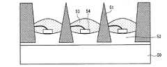
図11は、LTCC(低温同時焼成セラミックス)基板を使用した従来の発光装置を示す断面図である(特許文献1参照)。上記発光装置は、LTCC基板50、銀エポキシ52、反射障壁51、透明エポキシ53、およびLEDダイ54から成っている。本従来例において、LEDダイ54からの出射光は反射障壁51によって反射され、出射光のロスが低減されている。またLEDダイ54からの熱は、反射障壁51によって、関連する熱拡散部(図示せず)、及びLTCC基板50に放熱される。LTCC基板を用いた発光装置のLTCCパッケージングは、密に詰め込まれたLEDダイまたはLEDアレイによって発生した熱を分散するのに特に適する。 FIG. 11 is a cross-sectional view showing a conventional light emitting device using an LTCC (low temperature co-fired ceramics) substrate (see Patent Document 1). The light emitting device includes an
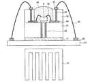
図12は、ワイヤボンディングを有するLTCCチップキャリアを示す断面図である(特許文献2参照)。このLTCCチップキャリアはマザーボード65上に順にヒートスプレッダ67、第2層LTCC61、及び頂部層LTCC60を備えている。頂部層LTCC60は中央に空洞を有している。空洞内には第2層LTCC61を貫くように形成された熱的ビア62上に、1つのLEDチップ4が接着剤等で固定されている。LEDチップ4は第2層LTCC61上に形成された第2層端子64に、ワイヤ90によりワイヤ・ボンディング接続されている。第2層端子64は、頂部層LTCC60上に形成された頂部端子63にビア68を介して接続されている。さらに頂部端子63は、マザーボード65上に形成された外部端子66に、ワイヤ91によりワイヤ・ボンディング接続されている。頂部端子63、第2層端子64、外部端子66、及びヒートスプレッダ67は同時焼成可能な導体により形成される。LEDチップを含む頂部層LTCC60内の空洞は、エポキシ樹脂69または他の有機材料によって封止される。さらに熱散逸のために、マザーボード65の下側に、種々の方法によってヒートシンク70が設置される。 FIG. 12 is a cross-sectional view showing an LTCC chip carrier having wire bonding (see Patent Document 2). The LTCC chip carrier includes a
LTCCは、有機材料より高い固有の熱伝導率を有している。また熱的ビア62及びメタライゼーションされた導体面を備えることでさらに熱伝導率を高め、発光装置の放熱性を改善することができる。 LTCC has a higher intrinsic thermal conductivity than organic materials. Further, by providing the thermal via 62 and the metallized conductor surface, the thermal conductivity can be further increased and the heat dissipation of the light emitting device can be improved.
また、LEDの発光効率を向上するための技術として、LEDの発光層と支持基板との間に、金属反射層を設ける技術が提案されている(非特許文献1参照)。これは、LEDから照射される支持基板側への光を金属反射層が反射することにより、LEDの発光量を高めることができるというものである。
しかしながら、上記従来の構成では、下記の問題を生じる。 However, the conventional configuration causes the following problems.
LTCC基板は、セラミックスとガラスとの複合材料から成る基板である。材料によってはLTCC基板がLEDチップからの光を透過または吸収することにより、発光出力の低下を招く。しかしながら、特許文献1、2に挙げた上記従来の構成では、LTCC基板表面での光反射および光透過対策については何ら対策がとられていない。また、上記従来の構成では、LEDチップ搭載面の横に段差がある構造をとっているため出射光のロスとなる。そのため、上記従来の構成は、ハイパワーLEDを実現する構成になっていない。 The LTCC substrate is a substrate made of a composite material of ceramics and glass. Depending on the material, the LTCC substrate transmits or absorbs light from the LED chip, leading to a decrease in light emission output. However, in the conventional configurations described in
また、非特許文献1が示す構成では、上記金属反射層は、例えば外界の水分または酸素等により、変質または劣化、さらにはそれに起因した反射率の低下が生じるという問題がある。 Further, in the configuration shown in Non-Patent Document 1, there is a problem that the metal reflective layer is altered or deteriorated due to, for example, external moisture or oxygen, and the reflectance is reduced due to it.
本発明は、上記の問題点に鑑みてなされたものであり、その目的は、光の取り出し効率を高くし、かつ、反射層の変質、劣化、ならびに反射率の低下を防ぐ発光装置を提供することにある。 The present invention has been made in view of the above problems, and an object of the present invention is to provide a light-emitting device that increases light extraction efficiency and prevents alteration and deterioration of the reflective layer and reduction in reflectance. There is.
本発明に係る発光装置は、基板上に光を出射する半導体装置及び複数の外部接続端子を有する発光装置において、前記基板上に形成され、前記半導体装置からの出射光を反射する光反射層と、少なくとも前記光反射層を被覆し、かつ、前記光反射層にて反射した光を透過する被覆層とを備え、前記半導体装置は、前記被覆層上に接着用樹脂を介して設置されるとともに、前記外部接続端子と接続部を介して電気的に接続されており、前記半導体装置と前記接続部とを覆うように封止樹脂で封止されている。
本発明に係る発光装置は、基板上に光を出射する半導体装置及び複数の外部接続端子を有する発光装置において、前記基板上に形成され、前記半導体装置からの出射光を反射する光反射層と、少なくとも前記光反射層を被覆し、かつ、前記光反射層にて反射した光を透過する被覆層とを備え、前記半導体装置は、前記被覆層上に形成されるとともに、前記外部接続端子と接続部を介して電気的に接続されており、前記半導体装置と前記接続部とを覆うように封止樹脂で封止されており、前記半導体装置は、発光ダイオードチップであり、前記被覆層は、ガラスから成り、前記接続部は配線パターン及びボンディングワイヤから成り、前記配線パターンは、前記基板上もしくは前記被覆層上に、互いに平行に、かつ、互いに距離をおいて形成され、前記半導体装置は、前記配線パターン間に複数設置されており、前記配線パターンと前記半導体装置とは前記ボンディングワイヤによって接続されている。
本発明に係る発光装置は、基板上に光を出射する半導体装置及び複数の外部接続端子を有し、前記基板上に形成され前記半導体装置からの出射光を反射する光反射層と、少なくとも前記光反射層を被覆し、かつ、前記光反射層にて反射した光を透過する被覆層とを備え、前記半導体装置は、前記被覆層上に形成されるとともに、前記外部接続端子と接続部を介して電気的に接続されており、前記半導体装置と前記接続部とを覆うように封止樹脂で封止されていることを特徴としている。A light emitting device according to the present invention is a semiconductor device that emits light on a substrate and a light emitting device having a plurality of external connection terminals. The light reflecting layer is formed on the substrate and reflects light emitted from the semiconductor device. A coating layer that covers at least the light reflection layer and transmits light reflected by the light reflection layer, and the semiconductor device is disposed on the coating layer via an adhesive resin. The external connection terminal is electrically connected through a connection portion, and is sealed with a sealing resin so as to cover the semiconductor device and the connection portion.
A light emitting device according to the present invention is a semiconductor device that emits light on a substrate and a light emitting device having a plurality of external connection terminals. The light reflecting layer is formed on the substrate and reflects light emitted from the semiconductor device. A coating layer that covers at least the light reflection layer and transmits the light reflected by the light reflection layer, and the semiconductor device is formed on the coating layer and has the external connection terminal It is electrically connected via a connection part, and is sealed with a sealing resin so as to cover the semiconductor device and the connection part, the semiconductor device is a light-emitting diode chip, and the covering layer is The connecting portion is made of a wiring pattern and a bonding wire, and the wiring pattern is formed on the substrate or the coating layer in parallel with each other and at a distance from each other. The semiconductor device has a plurality of installed between the wiring pattern, the said wiring pattern and the semiconductor device are connected by the bonding wire.
A light emitting device according to the present invention includes a semiconductor device that emits light on a substrate and a plurality of external connection terminals, a light reflecting layer that is formed on the substrate and reflects light emitted from the semiconductor device, and at least the A coating layer that covers the light reflection layer and transmits the light reflected by the light reflection layer, and the semiconductor device is formed on the coating layer and includes the external connection terminal and the connection portion. And is sealed with a sealing resin so as to cover the semiconductor device and the connection portion.
上記の構成によれば、半導体装置から下側(基板側)への出射光を光反射層が反射することにより、出射光のロスを減少させ有効に活用できるため、発光装置の発光量を高めることができ、光反射層を被覆層で被覆しているため光反射層の変質または劣化、さらにはそれに起因した反射率の低下を抑制するという効果を奏する。 According to the above configuration, since the light reflecting layer reflects the outgoing light from the semiconductor device to the lower side (substrate side), the loss of the outgoing light can be reduced and effectively used. In addition, since the light reflecting layer is covered with the coating layer, the light reflecting layer can be prevented from being deteriorated or deteriorated, and further, the reflectance can be prevented from decreasing.
前記光反射層は、90%以上の光反射率を有することが好ましい。 The light reflecting layer preferably has a light reflectance of 90% or more.
上記の構成によれば、光反射層が高い光反射率を有するためさらに発光装置の発光量を増すことができる。 According to said structure, since the light reflection layer has a high light reflectance, the emitted light amount of a light-emitting device can be increased further.
前記光反射層は、銀、または銀を主成分とする銀合金から成ることが好ましい。 The light reflecting layer is preferably made of silver or a silver alloy containing silver as a main component.
上記の構成によれば、銀または銀合金層で光反射層を形成することにより、半導体装置の発熱を基板の面方向に放散し、発光装置の放熱性を高めることができる。これにより、発光装置の発熱による色ズレを抑制することができる。 According to said structure, by forming a light reflection layer with a silver or silver alloy layer, the heat_generation | fever of a semiconductor device can be dissipated in the surface direction of a board | substrate, and the heat dissipation of a light-emitting device can be improved. Thereby, the color shift by the heat_generation | fever of a light-emitting device can be suppressed.
本発明に係る発光装置は、前記基板が、セラミックスを基材としてもよい。さらに前記基板は、低温同時焼成セラミックスを基材としてもよい。 In the light emitting device according to the present invention, the substrate may have ceramic as a base material. Furthermore, the substrate may be made of a low-temperature co-fired ceramic.
上記の構成によれば、低温同時焼成セラミックスは一般の有機材料より熱伝導率が高いため、発光装置の放熱性をさらに高めることができ、半導体装置の集積化を可能とする。
本発明に係る発光装置では、前記被覆層は前記基板表面と接触しており、前記被覆層及び前記基板は、共に、構成材料にガラス材料を含んでもよい。According to the above configuration, since the low-temperature co-fired ceramic has higher thermal conductivity than a general organic material, the heat dissipation of the light-emitting device can be further increased, and the semiconductor device can be integrated.
In the light emitting device according to the present invention, the coating layer is in contact with the substrate surface, and both the coating layer and the substrate may include a glass material as a constituent material.
本発明に係る発光装置は、前記基板が、ガラス粉末とセラミック粉末とを材料として焼成したものであることが好ましい。前記ガラス粉末は、例えばシリカガラス、ソーダ石灰ガラス、ほう珪酸ガラス、アルミノホウ珪酸ガラス、ほう珪酸亜鉛ガラス、アルミノ珪酸ガラスまたは燐酸ガラスを含むものを使用することができる。また前記セラミック粉末は、例えばSiO2、Al2O3、ZrO2、TiO2、ZnO、MgAl2O4、ZnAl2O4、MgSiO3、MgSiO4、Zn2SiO4、Zn2TiO4、SrTiO3、CaTiO3、MgTiO3、BaTiO3、CaMgSi2O6、SrAl2Si2O8、BaAl2Si2O8、CaAl2Si2O8、Mg2Al4Si5O18、Zn2Al4Si5O18、AlN、SiC、ムライトまたはゼオライトを含むものを使用することができる。In the light-emitting device according to the present invention, it is preferable that the substrate is fired using glass powder and ceramic powder as materials. As the glass powder, for example, one containing silica glass, soda lime glass, borosilicate glass, aluminoborosilicate glass, zinc borosilicate glass, aluminosilicate glass or phosphate glass can be used. The ceramic powder is, for example, SiO2 , Al2 O3 , ZrO2 , TiO2 , ZnO, MgAl2 O4 , ZnAl2 O4 , MgSiO3 , MgSiO4 , Zn2 SiO4 , Zn2 TiO4 , SrTiO4 .3 , CaTiO3 , MgTiO3 , BaTiO3 , CaMgSi2 O6 , SrAl2 Si2 O8 , BaAl2 Si2 O8 , CaAl2 Si2 O8 , Mg2 Al4 Si5 O18 , Zn2 Al4 Those containing Si5 O18 , AlN, SiC, mullite or zeolite can be used.
本発明に係る発光装置は、前記被覆層がガラスから成り、前記ガラスは、例えばシリカガラス、ソーダ石灰ガラス、ほう珪酸ガラス、アルミノホウ珪酸ガラス、ほう珪酸亜鉛ガラス、アルミノ珪酸ガラスまたは燐酸ガラスを含むものを使用することができる。 In the light emitting device according to the present invention, the covering layer is made of glass, and the glass includes, for example, silica glass, soda lime glass, borosilicate glass, aluminoborosilicate glass, borosilicate zinc glass, aluminosilicate glass, or phosphate glass. Can be used.
上記の構成によれば、基板及び被覆層がガラス粉末を含んでおり、基板と被覆層との密着性が良好になり、光反射層の劣化等による経年変化をさらに抑制し、反射率の低下を抑制することができる。特にほう珪酸ガラス(Na2O−B2O3−SiO2)は熱膨張係数が小さく、熱衝撃温度が高く、酸化ホウ素が多く含まれているため化学的な耐久性が高いため、さらに光反射層を保護する効果が高い。According to said structure, a board | substrate and a coating layer contain glass powder, the adhesiveness of a board | substrate and a coating layer becomes favorable, further suppresses the secular change by deterioration of a light reflection layer, etc., and a reflectance falls Can be suppressed. In particular, borosilicate glass (Na2 O—B2 O3 —SiO2 ) has a low thermal expansion coefficient, a high thermal shock temperature, and a high chemical durability because it contains a large amount of boron oxide. The effect of protecting the reflective layer is high.
本発明に係る発光装置は、前記半導体装置が、発光ダイオードチップであり、前記被覆層は、ガラスから成り、前記接続部は配線パターン及びボンディングワイヤから成り、前記配線パターンは、前記基板上もしくは前記被覆層上に、互いに平行に、かつ、互いに距離をおいて形成され、前記半導体装置は、前記配線パターン間に複数設置されており、前記配線パターンと前記半導体装置とは前記ボンディングワイヤによって接続されていてもよい。 In the light emitting device according to the present invention, the semiconductor device is a light emitting diode chip, the covering layer is made of glass, the connecting portion is made of a wiring pattern and a bonding wire, and the wiring pattern is formed on the substrate or the above A plurality of the semiconductor devices are disposed between the wiring patterns on the coating layer in parallel to each other and at a distance from each other, and the wiring patterns and the semiconductor devices are connected by the bonding wires. It may be.
上記の構成によれば、半導体装置の数を自由に調整することができ、発光装置の輝度調整、色度調整、及び発熱対策が容易になる。
本発明に係る発光装置では、前記被覆層及び前記基板に含まれる上記ガラス材料は同組成の材料であってもよい。According to said structure, the number of semiconductor devices can be adjusted freely and the brightness | luminance adjustment of a light-emitting device, chromaticity adjustment, and the countermeasure against heat_generation | fever become easy.
In the light emitting device according to the present invention, the glass material contained in the coating layer and the substratebut it may also be a material of the samecomposition.
本発明に係る発光装置は、前記基板内に、前記光反射層、前記外部接続端子、もしくはその双方とそれぞれ接合される、金属から成る放熱ビアを備えていることが好ましい。 The light-emitting device according to the present invention preferably includes a heat dissipation via made of metal that is bonded to the light reflecting layer, the external connection terminal, or both in the substrate.
上記の構成によれば、光反射層または外部接続端子、に接続された放熱ビアにより、発光装置の放熱性をさらに高めることができる。 According to said structure, the heat dissipation of a light-emitting device can further be improved with the thermal radiation via connected to the light reflection layer or the external connection terminal.
前記放熱ビアは、前記基板表面に対して垂直方向に形成されていることが好ましい。 The heat dissipation via is preferably formed in a direction perpendicular to the substrate surface.
さらに前記放熱ビアは、銀、または銀を主成分とする銀合金から成ることが好ましい。 Further, the heat dissipation via is preferably made of silver or a silver alloy containing silver as a main component.
上記の構成によれば、光反射層による基板平面方向への放熱に加え、基板垂直方向への放熱性が高まるため、発光装置の放熱性がさらに高まる。これにより小領域への半導体装置の集積化が可能となる。 According to the above configuration, in addition to the heat radiation in the substrate plane direction by the light reflecting layer, the heat radiation property in the substrate vertical direction is enhanced, so that the heat radiation property of the light emitting device is further enhanced. As a result, the semiconductor device can be integrated in a small area.
本発明に係る発光装置は、前記配線パターンは金から成ることが好ましい。 In the light emitting device according to the present invention, the wiring pattern is preferably made of gold.
上記の構成によれば、配線パターンが金で形成されているため、配線パターンの劣化等による経年変化を抑制することができる。 According to said structure, since the wiring pattern is formed with gold | metal | money, secular change by deterioration etc. of a wiring pattern can be suppressed.
本発明に係る発光装置は、前記配線パターンと前記被覆層との間に、ニッケルまたはクロム層が形成されていることが好ましい。 In the light emitting device according to the present invention, it is preferable that a nickel or chrome layer is formed between the wiring pattern and the covering layer.
上記の構成によれば、ガラスからなる被覆層と配線パターンとの密着性が向上し、配線パターンの劣化等による経年変化を抑制することができる。 According to said structure, the adhesiveness of the coating layer which consists of glass, and a wiring pattern improves, and secular change by deterioration etc. of a wiring pattern can be suppressed.
本発明に係る発光装置は、前記半導体装置が、前記被覆層上に接着用樹脂を介して設置されていてもよい。 In the light emitting device according to the present invention, the semiconductor device may be installed on the coating layer via an adhesive resin.
本発明に係る発光装置は、前記封止樹脂は、蛍光体を含んでいることが好ましい。 In the light emitting device according to the present invention, the sealing resin preferably contains a phosphor.
上記の構成によれば、蛍光体が半導体装置からの光を吸収し、別の波長の光を発することにより、単一光を発する半導体装置を用いてそれ以外の光(例えば白色光)を発する発光装置を得ることができる。 According to the above configuration, the phosphor absorbs light from the semiconductor device and emits light of another wavelength, so that other light (for example, white light) is emitted using the semiconductor device that emits single light. A light emitting device can be obtained.
本発明に係る発光装置は、前記封止樹脂は、蛍光体を含んでいる蛍光体含有樹脂部、及び前記蛍光体含有樹脂部を覆うように形成されている透明樹脂部、により構成されていることが好ましい。 In the light emitting device according to the present invention, the sealing resin includes a phosphor-containing resin portion containing a phosphor and a transparent resin portion formed so as to cover the phosphor-containing resin portion. It is preferable.
上記の構成によれば、蛍光体含有樹脂部を透明樹脂部によって保護することができる。 According to said structure, a fluorescent substance containing resin part can be protected by a transparent resin part.
本発明に係る発光装置は、前記封止樹脂の外形形状がドーム型であることが好ましい。 In the light emitting device according to the present invention, the outer shape of the sealing resin is preferably a dome shape.
本発明に係る発光装置は、前記蛍光体含有樹脂部の外形形状、及び前記透明樹脂部の外形形状がドーム型であることが好ましい。 In the light-emitting device according to the present invention, it is preferable that the outer shape of the phosphor-containing resin portion and the outer shape of the transparent resin portion be a dome shape.
上記の構成によれば、封止樹脂の光照射方向側に角となる部分がないので、照射光の屈折方向が連続的に変化する。よって、照射光の強度のむらが低減できるという効果を奏する。 According to said structure, since there is no corner | angular part in the light irradiation direction side of sealing resin, the refractive direction of irradiation light changes continuously. Therefore, there is an effect that unevenness of the intensity of irradiation light can be reduced.
本発明に係る発光装置は、発光ダイオードチップと、該発光ダイオードチップをチップ載置部にダイボンディングするとともに、前記発光ダイオードチップの出射光を反射する銀反射層を備えたパッケージと前記発光ダイオードチップを被覆する封止樹脂を備えた発光装置であって、前記銀反射層はガラス層により被覆されてなることを特徴とする。 A light-emitting device according to the present invention includes a light-emitting diode chip, a package including a silver reflective layer for die-bonding the light-emitting diode chip to a chip mounting portion and reflecting light emitted from the light-emitting diode chip, and the light-emitting diode chip A light emitting device comprising a sealing resin for coating the silver reflective layer, wherein the silver reflective layer is coated with a glass layer.
本発明に係る発光装置は、前記封止樹脂の材質がジメチルシリコーンもしくはメチルゴムであることが好ましい。 In the light emitting device according to the present invention, it is preferable that a material of the sealing resin is dimethyl silicone or methyl rubber.
本発明に係る発光装置は、前記封止樹脂は前記発光ダイオードチップから発する1次光の少なくとも一部を吸収して前記1次光よりも長波長の2次光に変換する蛍光体を分散させたものであることが好ましい。 In the light emitting device according to the present invention, the sealing resin disperses a phosphor that absorbs at least part of the primary light emitted from the light emitting diode chip and converts it into secondary light having a longer wavelength than the primary light. It is preferable that
本発明に係る発光装置は、前記銀反射層が、前記発光装置の出射面の周縁部に形成されることが好ましい。 In the light emitting device according to the present invention, it is preferable that the silver reflective layer is formed on a peripheral portion of an emission surface of the light emitting device.
本発明に係る発光装置は、前記チップ載置部に凹陥部が形成され、前記凹陥部の底面に電極パッドが形成されることが好ましい。 In the light emitting device according to the present invention, it is preferable that a recess is formed in the chip mounting portion, and an electrode pad is formed on the bottom surface of the recess.
本発明に係る発光装置用パッケージの製造方法は、アルミナを主材料とする複数のグリーンシートを準備する工程と、前記グリーンシートの一部に孔開け加工する工程と、前記孔に金属ペーストまたはガラスペーストの少なくとも一方を充填する工程と、前記複数のグリーンシートを、前記金属ペーストが前記ガラスペーストにより被覆されるように積層し焼成する工程を順に有する。 A method for manufacturing a package for a light emitting device according to the present invention includes a step of preparing a plurality of green sheets mainly made of alumina, a step of punching a part of the green sheet, and a metal paste or glass in the holes. A step of filling at least one of the pastes and a step of laminating and firing the plurality of green sheets so that the metal paste is covered with the glass paste are sequentially provided.
本発明に係る発光装置は、基板上に光を出射する半導体装置及び複数の外部接続端子を有し、前記基板上に形成され前記半導体装置からの出射光を反射する光反射層と、少なくとも前記光反射層を被覆し、かつ、前記光反射層にて反射した光を透過する被覆層とを備え、前記半導体装置は、前記被覆層上に形成されるとともに、前記外部接続端子と接続部を介して電気的に接続されており、前記半導体装置と前記接続部とを覆うように封止樹脂で封止されていることを特徴としている。 A light emitting device according to the present invention includes a semiconductor device that emits light on a substrate and a plurality of external connection terminals, a light reflecting layer that is formed on the substrate and reflects light emitted from the semiconductor device, and at least the A coating layer that covers the light reflection layer and transmits the light reflected by the light reflection layer, and the semiconductor device is formed on the coating layer and includes the external connection terminal and the connection portion. And is sealed with a sealing resin so as to cover the semiconductor device and the connection portion.
上記の構成によれば、半導体装置から下側(基板側)への出射光を光反射層が反射することにより、出射光のロスを減少させ有効に活用できるため発光装置の発光量を高めることができ、光反射層を被覆層で被覆しているため光反射層の変質、または劣化、さらにはそれに起因した反射率の低下を抑制するという効果を奏する。 According to the above configuration, the light reflection layer reflects the outgoing light from the semiconductor device to the lower side (substrate side), thereby reducing the loss of the outgoing light and increasing the amount of light emitted from the light emitting device. In addition, since the light reflection layer is covered with the coating layer, the light reflection layer can be prevented from being deteriorated or deteriorated, and further, the reflectance can be prevented from lowering.
また、本発明に係る発光装置は、上記光反射層を被覆層によって十分保護しているため、封止樹脂として、ガス封止性がやや低い場合があるものの、耐熱性が高く、ガラスとの密着性が高いジメチルシリコーンやメチルゴムを好適に用いることができる。 Moreover, since the light-emitting device according to the present invention sufficiently protects the light reflecting layer with a coating layer, the sealing resin may have a slightly low gas sealing property, but has a high heat resistance and is not Dimethyl silicone or methyl rubber having high adhesion can be preferably used.
本発明に係る発光装置用パッケージの製造方法は、グリーンシートを積層した基板素材を焼成すると同時に反射層とその被覆層を焼成して発光装置用パッケージを製造するものであるため、焼成工程が1回で済み低コストになる。 The method for manufacturing a light emitting device package according to the present invention is a method for manufacturing a light emitting device package by firing a substrate material on which green sheets are laminated and simultaneously firing a reflective layer and its coating layer. Saves time and costs.
[実施の形態1]
図1に本発明の実施の形態の一つによる発光装置1000を上面から見た模式図を示す。発光装置1000は、低温同時焼成セラミックス(LTCC)基板1上に、順に銀反射層(図示せず)及びガラス層(被覆層)3が形成された構造を持ち、その上に発光部1001を備えている。発光部1001は蛍光体含有封止樹脂6で封止されている。LTCC基板1上にはさらに、正電極外部接続端子8及び負電極外部接続端子7が設けられており、それぞれの外部接続端子には外部配線15が接続されている。外部配線15はLTCC基板1に設けられた外部配線用穴16を通って外部に配線される。LTCC基板1は発光装置1000をネジによって他の装置へ固定するための取り付け部13を有する。ここで、発光装置1000の外形形状をほぼ正方形状にし、発光部1001の形状はほぼ長方形状とした。[Embodiment 1]
FIG. 1 shows a schematic view of a
図2は発光装置1000の配線パターン等を示す平面図である。LTCC基板1上に形成されたガラス層3の上に、細長い長方形状の配線パターン(接続部)9が互いに平行に、かつ、互いに距離をおいて複数形成されている。配線パターン9は正電極外部接続端子8と、負電極外部接続端子7とに接続されている。配線パターン9間にはLEDチップ(半導体装置)を搭載するためのチップ載置部41が設けられている。 FIG. 2 is a plan view showing a wiring pattern and the like of the
図3(a)〜図3(d)及び図4は発光装置1000の製造方法を示す概略断面図である。 FIG. 3A to FIG. 3D and FIG. 4 are schematic sectional views showing a method for manufacturing the
(a)厚さ2mmのLTCC基板1上に、メッキ法を用いて銀膜を形成し、厚さ0.2mmの銀反射層(光反射層)2を形成する。 (A) A silver film is formed on the LTCC substrate 1 having a thickness of 2 mm by using a plating method to form a silver reflecting layer (light reflecting layer) 2 having a thickness of 0.2 mm.
前記銀反射層2上に厚さ0.006mmのガラス層3を形成する。 A
前記ガラス層3上にスクリーン印刷法を用いて配線パターン9(厚さ0.07mm、幅0.45mm、間隔2mm)を形成する。ここではガラス層の表面粗化を行うことなくガラス表面を清浄化して湿潤性を与え、次に化学的結合を強化する特殊な処理をした後、触媒活性化し、ガラス素材用に調整された無電解ニッケルめっきを直接施す方法を用いた。 A wiring pattern 9 (thickness 0.07 mm, width 0.45 mm,
ここで、LTCC基板1は、ほう珪酸ガラス(Na2O−B2O3−SiO2)とSiO2との混合材料から成っている。銀反射層2は、銀、または銀を主成分とする銀合金(Ag、AgPt、Ag−Bi、Ag−Nd系合金)から成っている。ガラス層3は、透明ほう珪酸ガラス(Na2O−B2O3−SiO2)をドクターブレード法(セラミックスをシート状に成形する方法の一つ。キャリヤ(キャリヤフィルム、エンドレスベルト)上に載せて運ばれるスリップ(原料粉末を溶剤に分散してスラリー化したその泥漿)の厚さをナイフエッジ(ドクターブレード)とキャリヤとの間隔を調節することによって精密に制御して作製できる成形方法。参考:http://www.oit.ac.jp/www-ee/server/aplab/res/slurry.html)を用いて作製した。Here, the LTCC substrate 1 is made of a mixed material of borosilicate glass (Na2 O—B2 O3 —SiO2 ) and SiO2 . The
(b)ガラス層3上の配線パターン9の間にLEDチップ4(短辺幅0.24mm、長辺0.48mm、厚み0.14mm、36個)をシリコーン樹脂を用いて固定する。次いで、LEDチップ4と配線パターン9をボンディングワイヤ(接続部)Wを用いて電気的に接続する。なお、LEDチップ4は、一般的に用いられているLEDチップの構成を備えている。 (B) LED chips 4 (short side width 0.24 mm, long side 0.48 mm, thickness 0.14 mm, 36 pieces) are fixed between the
(c)LEDチップ4が設置された領域を囲うように略長方形状のシリコーンゴムシート5を配置し、ガラス層3上に密着させる。 (C) A substantially rectangular
(d)次に、シリコーンゴムシート5内に蛍光体(Eu:BOSE((Ba・Sr)2SiO4:Eu))を含む封止樹脂(シリコーン)6を注入し、この蛍光体を含む封止樹脂を熱硬化させる。(D) Next, a sealing resin (silicone) 6 containing a phosphor (Eu: BOSE ((Ba · Sr)2 SiO4 : Eu)) is injected into the
蛍光物質と透光性樹脂であるシリコーン樹脂とが混合されたものを前記シリコーンゴムシート5の枠内に注入した後、30分間温度を150℃に保持し樹脂を硬化させ、蛍光体を含む封止樹脂6を形成する。その後シリコーンゴムシート5を取り除く。 After injecting a mixture of a fluorescent substance and a silicone resin, which is a translucent resin, into the frame of the
図4は、こうしてLTCC基板1上に形成された発光部1001を示す断面図である。 FIG. 4 is a cross-sectional view showing the
蛍光体を含有した封止樹脂6から、CIEの色度表でx、y=(0.345、0.35)となる光が得られるように形成した。こうして、発光部1001が製造される。 The sealing
前記のように構成することで、LEDチップ4からの出射光のうち、特に、下面(基板側)方向からの光はLTCC基板1とガラス層3とで挟まれた銀反射層2で反射されるので、LEDチップ4からの出射光がロスなく有効に活用される。したがって発光装置1000の発光量を高めることができる。また、銀反射層2は、光反射層としての機能と、LEDチップ4で発生した熱をパッケージの面方向(LTCC基板1に対し水平方向)に放散させる機能とを持つ。また、熱伝導率が高く放熱性のよいLTCC基板1を用いているために、LEDチップ4の集積化が可能となる。したがって、熱による発光装置の変形を抑えることができ、色ズレなどを抑制することができる。 With the configuration as described above, among the light emitted from the
また本実施の形態では、銀反射層2をガラス層3で覆っているので、反射層の変質、劣化、及び反射率の低下を抑制することができる。ガラス層3は一般の樹脂に比べ酸素または水分等に対する隔絶性が高く、銀反射層2の経年変化を抑制することができる。またLTCC基板1及びガラス層3がともにガラスを含んでおり、基板とガラス層との密着性が良好になるため、銀反射層2を酸素または水分等から隔絶する効果がさらに高い。 Moreover, in this Embodiment, since the
反射層の材料としては前記した銀または銀合金の他に、LEDチップからの出射光を反射する任意の金属または非金属の材料を用いることができる。例えば、90%以上の光反射率を有する任意の金属または非金属の材料を用いると、LTCC基板1側への出射光を有効に活用でき、発光部1001の発光量を高めることができる。 As the material of the reflective layer, any metal or non-metal material that reflects the light emitted from the LED chip can be used in addition to the above-described silver or silver alloy. For example, when an arbitrary metal or non-metal material having a light reflectance of 90% or more is used, the emitted light toward the LTCC substrate 1 can be effectively used, and the light emission amount of the
また、配線パターン9としては化学的に安定な金を含む材料をもちいることが好ましい。さらに本実施の形態では配線パターン9とガラス層3との間にニッケル層を形成しているので、金から成る配線パターン9とガラス層3との密着性が向上し、配線パターン9の劣化等による経年変化をさらに抑制することができる。またニッケル層の代わりにクロム層を形成してもよい。 The
ここで、ガラス層3及びLTCC基板1の材料としてのガラス粉末は、Na2O−B2O3−SiO2の組成から成るホウケイ酸ガラスが好ましい。熱膨張係数が小さく、熱衝撃温度が高く、酸化ホウ素が多く含まれているため化学的に大変耐久性があるためである。Here, the glass powder as a material of the
シリコーンゴムシート5(図3(d)参照)は蛍光体を含有した透光性樹脂を塗布する際のダム(樹脂漏れを防ぐ)のような機能を有している。従って、前記シリコーンゴムシート5はダムシートと呼べるような特徴を有している。また、前記ダムシートは、何度も使用することが可能である。また、前記ダムシートの形状を変えることにより発光部1001の形状(蛍光体含有封止樹脂6の形状)を容易に様々な形状に変えられることを特徴としている。 The silicone rubber sheet 5 (see FIG. 3D) has a function like a dam (prevents resin leakage) when a translucent resin containing a phosphor is applied. Therefore, the
ガラス層3及び銀反射層2は、シリコーンゴムシート5で囲われているLEDチップ4の搭載面全面にわたって形成されている。 The
ここで、LEDチップ4の載置領域を本構成のようにすることにより、LEDチップ4の載置ピッチを配線パターン9との平行方向に沿って自在に決めることができるために、発光装置の輝度調整、色度調整、及び発熱対策が容易にできる。 Here, by setting the mounting area of the
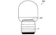
発光装置1000を用いて作製した照明器具の応用例として、図5に蛍光灯形LEDランプ7000、図6に電球形LEDランプ9000の模式図を示す。電球形LEDランプ9000は口金14を有している。蛍光灯形LEDランプ7000ならびに電球形LEDランプ9000の構成は、発光装置1000を備えていること以外は一般的な蛍光灯形LEDランプならびに電球形LEDランプの構成と同様である。 As an application example of a lighting fixture manufactured using the
[実施の形態2]
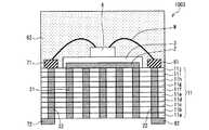
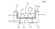
図7(a)は本発明の他の実施の形態による発光装置1002を示す模式断面図であり、図7(b)はその平面図である。なお、説明の便宜上、実施の形態1で用いた部材と同一の機能を有する部材には同一の部材番号を付記し、その説明を省略する。発光装置1002は、低温同時焼成セラミックス(LTCC)基板10、LTCC基板10上に形成された銀反射層2、銀反射層2を覆うガラス層3、ガラス層3の上に設置されたLEDチップ4、及びガラス層3の上に形成された正電極外部接続端子81と負電極外部接続端子71と、から成る。LEDチップ4とそれぞれの外部接続端子81、71はボンディングワイヤWで電気接続されている。LEDチップ4とボンディングワイヤWとはドーム状の蛍光体含有封止樹脂61で封止されている。外部接続端子81、71はLTCC基板10のそれぞれ反対側の側面まで延びて形成されている。[Embodiment 2]
FIG. 7A is a schematic cross-sectional view showing a
LTCC基板10は多層(10層)のLTCC層10a〜10jから成っており、銀で形成された複数の放熱ビア21が、LTCC基板10の各層を貫通して、すなわちLTCC基板10に対して垂直方向に、それぞれ形成され、かつ、それぞれ銀反射層2に接続されている。ここで、LTCC基板10はグリーンシートを10枚積層して作製される。尚、本実施の形態はLEDチップ4を4個設置したものであるが、図7(a)には簡単のため1つのLEDチップの断面を示す。 The
以下に発光装置1002の製造方法を示す。 A method for manufacturing the
工程(1):セラミックス粉末(Al2O3粉末 30重量%)とガラス粉末(ほう珪酸ガラス粉末 70重量%)とを一定比率で配合・混合し原料とする。混合された原料に有機系のバインダ(アクリル樹脂)と溶剤(トルエン)とを加え、均一になるまで分散させ、スラリーと呼ばれるグリーンシートのもとになる材料を作製する。スラリーはドクターブレード成形機でPETフィルム上に一定の厚さで塗布され、乾燥工程を経て巻き取られる。ここで作製されたシート状の材料はグリーンシート(厚さ0.1mm)と呼ばれる。前記グリーンシートを最適な大きさに切断する。放熱ビア21用のビアとなる穴開け加工(パンチング加工)を施す。前記の穴へ放熱材料(銀ペースト)を充填し、一層のLTCC層(厚さ0.1mm)を作製する。こうして作製された各LTCC層(10a,10b,10c,10d,10e,10f,10g,10h,10i,10j)を積層(10層)し、加熱圧着し、焼成工程(850℃)を経てLTCC基板10が作製される。Step (1): Ceramic powder (Al2 O3 powder 30% by weight) and glass powder (
工程(2):LTCC基板10(厚さ1mm)上に、銀膜(厚さ0.25mm)をメッキ法を用いて形成し、銀反射層2を形成する。ここで、グリーンシートのガラス粉末としてほう珪酸ガラス(Na2O−B2O3−SiO2)、セラミックス粉末としてAl2O3を用いた。Step (2): On the LTCC substrate 10 (thickness 1 mm), a silver film (thickness 0.25 mm) is formed using a plating method, and the silver
工程(3):前記銀反射層2上にガラス層3(厚さ0.01mm)を形成する。ここで、ガラス層3は、透明ほう珪酸ガラス(Na2O−B2O3−SiO2)をドクターブレード法を用いて作製した。Step (3): A glass layer 3 (thickness: 0.01 mm) is formed on the silver
工程(4):前記ガラス層3上にスクリーン印刷法を用いて外部接続端子71、81(厚さ0.7mm、幅0.45mm)を金で形成する。 Step (4):
工程(5):ガラス層3上にLEDチップ4(短辺幅0.24mm、長辺0.48mm、厚み0.14mm、4個)をシリコーン樹脂(図示せず)を用いて固定する。次いでLEDチップ4と外部接続端子71、81とを、ボンディングワイヤWを用いて電気的接続する。 Step (5): The LED chip 4 (short side width 0.24 mm, long side 0.48 mm, thickness 0.14 mm, 4 pieces) is fixed on the
工程(6)次に、蛍光体(Eu:BOSE)を含む封止樹脂(シリコーン)61を形成し、この蛍光体含有封止樹脂61を熱硬化させる。蛍光体含有封止樹脂61は、蛍光物質と透光性樹脂であるシリコーン樹脂とを混合したものを、30分間温度を150℃に保持し樹脂を硬化させ形成される。尚、本実施の形態では蛍光体含有封止樹脂61がCIEの色度表でx、y=(0.345、0.35)となる光が得られるように形成した。こうして発光部が製造される。 Step (6) Next, a sealing resin (silicone) 61 containing a phosphor (Eu: BOSE) is formed, and the phosphor-containing
ここで銀反射層2はLEDチップ4からLTCC基板10の方向へ出射された光を外部へ取り出すのに有効である。また本実施の形態では、銀反射層2をガラス層3で覆っているので、反射層の変質、劣化、及び反射率の低下を抑制することができる。ガラス層3は一般の樹脂に比べ酸素または水分等に対する隔絶性が高く、銀反射層2の経年変化を抑制することができる。 Here, the
また、銀で形成された放熱ビア21はLEDチップ4から生じる熱を基板の垂直方向へ伝えるために、効果的に外部に放熱させることができる。この効果は、銀反射層2と放熱ビア21とが接触していることによって、LEDチップ4から発生した熱が銀反射層2を介して放熱ビア21に効率よく伝わるために、より顕著となる。放熱ビア21は、銀だけでなく、任意の金属で形成することができる。また銀反射層2と同じように銀を主成分とする銀合金(AgPt、Ag−Bi、Ag−Nd系合金)によって形成してもよい。 In addition, the heat dissipation via 21 formed of silver can effectively dissipate the heat to the outside in order to transfer the heat generated from the
また、発光装置1002のLTCC基板10の下側にヒートシンク(図示せず)を設置してもよい。それにより、さらに発光装置の放熱性を高め、発熱による色ズレを抑制することができる。その際、放熱ビア21はヒートシンクと接触していることが好ましい。 Further, a heat sink (not shown) may be installed below the
なお、放熱ビア21は、LTCC基板10内に透過してきたLEDチップ4からの光を反射する効果があり、LTCC基板10表面から見て銀反射層2が形成されていない領域に放熱ビア21を延ばして配置することで、LTCC基板10表面側への光の取り出しをさらに改善できる。 The heat dissipation via 21 has an effect of reflecting the light from the
[実施の形態3]
図8は本発明の他の実施の形態による発光装置1005を示す模式断面図である。なお、説明の便宜上、実施の形態2で用いた部材と同一の機能を有する部材には同一の部材番号を付記し、その説明を省略する。本実施の形態が実施の形態2と違うのは、蛍光体含有封止樹脂の代わりに、蛍光体を含んだ蛍光体含有樹脂部63と、蛍光体含有樹脂部63を覆うように形成された透明樹脂部64とからなるドーム形状の封止樹脂によって、LEDチップ4とボンディングワイヤWとが封止されている点である。蛍光体含有樹脂部63及び透明樹脂部64はそれぞれドーム形状をしている。[Embodiment 3]
FIG. 8 is a schematic cross-sectional view showing a
前記のように構成することで、蛍光体含有樹脂部63を透明樹脂部64によって保護することができる。また、封止樹脂及び各樹脂部がドーム形状であるため、LEDチップ4からの照射光の屈折方向は連続的に変化する。そのため、照射光の強度の空間的なむらを低減することができる。 By configuring as described above, the phosphor-containing
透明樹脂部64としては、透明度が確保でき、かつ硬度の高い素材を用いるのが好ましいが、材料に特に限定はない。 As the
[実施の形態4]
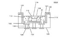
図9は本発明の他の実施の形態による発光装置1003を示す模式断面図である。なお、説明の便宜上、実施の形態2で用いた部材と同一の機能を有する部材には同一の部材番号を付記し、その説明を省略する。発光装置1003は、低温同時焼成セラミックス(LTCC)基板11、LTCC基板11上に形成された銀反射層2、LTCC基板11上で銀反射層2だけを覆うガラス層3、ガラス層3の上に設置されたLEDチップ4、及びLTCC基板11上に形成された正電極外部接続端子81と負電極外部接続端子71と、から成る。LEDチップ4とそれぞれの外部接続端子81、71とはボンディングワイヤWで電気接続されている。LEDチップ4とボンディングワイヤWと外部接続端子81,71とは蛍光体含有封止樹脂62で封止されている。LTCC基板11は多層(10層)のLTCC層11a〜11jから成り、銀で形成された複数の放熱ビア21が、各層を貫通して、すなわちLTCC基板11に対して垂直方向に、それぞれ形成され銀反射層2に接続されている。また、外部接続端子81、71はLTCC基板11を貫通する2つの配線ビア(放熱ビア)22にそれぞれ接続されており、各配線ビア22はLTCC基板11の下面側に形成された外部端子82、72にそれぞれ接続されている。ここで、LTCC基板11はグリーンシートを10枚積層して作製される。尚、本実施の形態はLEDチップ4を4個設置したものであるが、図9には簡単のため1つのLEDチップの断面を示す。[Embodiment 4]
FIG. 9 is a schematic cross-sectional view showing a
以下に発光装置1003の製造方法を示す。 A method for manufacturing the
工程(1):セラミックス粉末(Al2O3粉末 30重量%)とガラス粉末(ほう珪酸ガラス粉末 70重量%)を一定比率で配合・混合する。混合された原料に有機系のバインダ(アクリル樹脂)と溶剤(トルエン)とを加え、均一になるまで分散させ、スラリーと呼ばれるグリーンシートのもとになる材料を作製する。スラリーはドクターブレード成形機でPETフィルム上に一定の厚さで塗布され、乾燥工程を経て巻き取られる。ここで作製されたシート状の材料はグリーンシート(厚さ0.1mm)と呼ばれる。前記グリーンシートを最適な大きさに切断する。放熱ビア21及び配線ビア22用のビアとなる穴開け加工(パンチング加工)を施す。放熱ビア21及び配線ビア22となる穴へ材料(銀ペースト)を充填し、一層のLTCC層(厚さ0.1mm)を作製する。こうして作製された各LTCC層(11a,11b,11c,11d,11e,11f,11g,11h,11i,11j)を積層(10層)し、加熱圧着し、焼成工程(850℃)を経てLTCC基板11が作製される。 Step (1): Ceramic powder (Al2O3 powder 30% by weight) and glass powder (
工程(2):LTCC基板11(厚さ1mm)上に、銀膜2(厚さ0.25mm)をメッキ法を用いて形成し、銀反射層2を形成する。ここで、グリーンシートのガラス粉末としてほう珪酸ガラス(Na2O−B2O3−SiO2)、セラミックス粉末としてAl2O3を用いた。Step (2): On the LTCC substrate 11 (thickness 1 mm), a silver film 2 (thickness 0.25 mm) is formed using a plating method, and the silver
工程(3):前記銀反射層2上にガラス層3(厚さ0.007mm)を形成する。ここで、ガラス層3は、透明ほう珪酸ガラス(Na2O−B2O3−SiO2)をドクターブレード法を用いて作製した。Step (3): A glass layer 3 (thickness 0.007 mm) is formed on the silver
工程(4):前記LTCC基板11の配線ビア22上に、スクリーン印刷法を用いてガラス層3を挟むように外部接続端子81,71(厚さ0.7mm、幅0.45mm)を金で形成する。 Step (4):
工程(5):ガラス層3上にLEDチップ4(短辺幅0.24mm、長辺0.48mm、厚み0.14mm、4個)をシリコーン樹脂を用いて固定する。LEDチップ4と外部接続端子81,71とをボンディングワイヤWを用いて電気的接続する。 Step (5): The LED chip 4 (short side width 0.24 mm, long side 0.48 mm, thickness 0.14 mm, 4 pieces) is fixed on the
工程(6):次に、蛍光体(Eu:BOSE)を含む封止樹脂(シリコーン)62を形成し、この蛍光体含有封止樹脂62を熱硬化させる。蛍光体含有封止樹脂62は、蛍光物質と透光性樹脂であるシリコーン樹脂とを混合したものを、30分間温度を150℃に保持し樹脂を硬化させ形成される。尚、本実施の形態では、蛍光体含有封止樹脂62がCIEの色度表でx、y=(0.345、0.35)となる光が得られるように形成した。こうして発光部が製造される。 Step (6): Next, a sealing resin (silicone) 62 including a phosphor (Eu: BOSE) is formed, and the phosphor-containing
ここで、LEDチップ4からの熱がボンディングワイヤWを介して外部接続端子81,71に伝わる。LTCC基板11の下側に形成された外部端子82,72はそれぞれ外部接続端子81,71と配線ビア22を介して接続している。そのため、外部接続端子81,71に伝わった熱は外部端子82、72に伝わり放熱されることになる。この効果は、外部接続端子81,71と配線ビア22とが接触していることによって、LEDチップ4から発生した熱がボンディングワイヤWを介して配線ビア22に効率よく伝わるために、より顕著となる。配線ビア22は、銀だけでなく、任意の金属で形成することができる。また銀反射層2と同じように銀を主成分とする銀合金(AgPt、Ag−Bi、Ag−Nd系合金)によって形成してもよい。尚、LTCC基板11上の外部接続端子81,71に接続する配線ビア22を設けることができるのは、ガラス層3が銀反射層2だけを覆っているためである。 Here, heat from the
ここで銀反射層2はLEDチップ4からLTCC基板10の方向へ出射された光を外部へ取り出すのに有効である。また本実施の形態では、銀反射層2をガラス層3で覆っているので、反射層の変質、劣化、及び反射率の低下を抑制することができる。ガラス層3は一般の樹脂に比べ酸素または水分等に対する隔絶性が高く、銀反射層2の経年変化を抑制することができる。 Here, the
ここで、発光装置1003のLTCC基板11の下側にヒートシンク(図示せず)を設置してもよい。その際、放熱ビア21はヒートシンクと接触していることが好ましい。 Here, a heat sink (not shown) may be installed below the
[実施の形態5]
図10は本発明の他の実施の形態による発光装置1004を示す模式断面図である。なお、説明の便宜上、実施の形態4で用いた部材と同一の機能を有する部材には同一の部材番号を付記し、その説明を省略する。発光装置1004は、アルミナ基板12、アルミナ基板12上に形成された銀反射層2、銀反射層2だけを覆うガラス層3、ガラス層3の上に設置されたLEDチップ4、及びアルミナ基板12上に形成された正電極外部接続端子81と負電極外部接続端子71と、から成る。LEDチップ4とそれぞれの外部接続端子81、71とはボンディングワイヤWで電気接続されている。LEDチップ4とボンディングワイヤWと外部接続端子81,71とは蛍光体含有封止樹脂62で封止されているが、図10の奥行き方向に関しては、アルミナ基板12の全面を覆っているわけではない。アルミナ基板12上には正電極接続ランド81及び負電極接続ランド71を表面に露出させ、外部電源(図示せず)と接続できるようするために、封止されていない領域がある。尚、本実施の形態はLEDチップ4を36個設置したものであるが、図9には簡単のため1つのLEDチップの断面を示す。[Embodiment 5]
FIG. 10 is a schematic cross-sectional view showing a
以下に発光装置1004の製造方法を示す。 A method for manufacturing the
工程(1):アルミナ基板12(厚さ2mm)上に銀膜2(厚さ0.2mm)をメッキ法を用いて形成し、銀反射層2を形成する。 Step (1): A silver film 2 (thickness 0.2 mm) is formed on an alumina substrate 12 (
工程(2):前記銀反射層2上にガラス層3(厚さ0.006mm)を形成する。ここで、ガラス層3は、透明ほう珪酸ガラス(Na2O−B2O3−SiO2)をドクターブレード法を用いて作製した。Step (2): A glass layer 3 (thickness 0.006 mm) is formed on the silver
工程(3):前記アルミナ基板12上にスクリーン印刷法を用いて外部接続端子81,71(厚さ0.07mm、幅0.45mm、長さ2mm)を形成する。 Step (3):
工程(4):ガラス層3上にLEDチップ4(短辺幅0.24mm、長辺0.48mm、厚み0.14mm、36個)をシリコーン樹脂を用いて固定する。次いでLEDチップ4と外部接続端子81,71とをボンディングワイヤWを用いて電気的接続する。 Process (4): LED chip 4 (short side width 0.24mm, long side 0.48mm, thickness 0.14mm, 36 pieces) is fixed on the
工程(5):次に、蛍光体(Eu:BOSE)を含む封止樹脂(シリコーン)62を注入し、この蛍光体含有封止樹脂を熱硬化させる。蛍光体含有封止樹脂62は、蛍光物質と透光性樹脂であるシリコーン樹脂とを混合したものを、30分間温度を150℃に保持し樹脂を硬化させ形成される。尚、本実施の形態では、蛍光体含有封止樹脂62がCIEの色度表でx、y=(0.345、0.35)となる光が得られるように形成した。こうして発光部が製造される。 Step (5): Next, a sealing resin (silicone) 62 containing a phosphor (Eu: BOSE) is injected, and the phosphor-containing sealing resin is thermally cured. The phosphor-containing
また本実施の形態では、銀反射層2をガラス層3で覆っているので、反射層の変質、劣化、及び反射率の低下を抑制することができる。ガラス層3は一般の樹脂に比べ酸素または水分等に対する隔絶性が高く、銀反射層2の経年変化を抑制することができる。 Moreover, in this Embodiment, since the
また、ガラス層3上の外部接続端子81,71としては化学的に安定な金を含む材料をもちいることが好ましい。 The
各実施の形態において、ガラス層及びLTCC基板の材料であるガラス粉末としては、シリカガラス、ソーダ石灰ガラス、ほう珪酸ガラス、アルミノホウ珪酸ガラス、ほう珪酸亜鉛ガラス、アルミノ珪酸ガラス及び/または燐酸ガラスなどが挙げられ、特に、ほう珪酸系ガラスが好適である。 In each embodiment, the glass powder that is a material of the glass layer and the LTCC substrate includes silica glass, soda-lime glass, borosilicate glass, aluminoborosilicate glass, zinc borosilicate glass, aluminosilicate glass, and / or phosphate glass. In particular, borosilicate glass is suitable.
また、LTCC基板の材料であるセラミック粉末は、SiO2、Al2O3、ZrO2、TiO2、ZnO、MgAl2O4、ZnAl2O4、MgSiO3、MgSiO4、Zn2SiO4、Zn2TiO4、SrTiO3、CaTiO3、MgTiO3、BaTiO3、CaMgSi2O6、SrAl2Si2O8、BaAl2Si2O8、CaAl2Si2O8、Mg2Al4Si5O18、Zn2Al4Si5O18、AlN、SiC、ムライト及びゼオライトなどが挙げられる。また、LTCC基板は、セラミックスを基材とする基板に代替可能である。Moreover, the ceramic powder which is the material of the LTCC substrate is SiO2 , Al2 O3 , ZrO2 , TiO2 , ZnO, MgAl2 O4 , ZnAl2 O4 , MgSiO3 , MgSiO4 , Zn2 SiO4 ,
封止樹脂の材料としては、エポキシ樹脂、ユリア樹脂またはシリコーン樹脂などの耐候性に優れた透明樹脂、または、耐光性に優れたシリカゾルまたは硝子などの透光性無機材料、が好適に用いられる。また、封止樹脂には蛍光体と共に拡散剤を含有させても良い。具体的な拡散剤としては、チタン酸バリウム、酸化チタン、酸化アルミニウム、酸化珪素、炭酸カルシウム、または二酸化珪素等が好適に用いられる。 As the material of the sealing resin, a transparent resin excellent in weather resistance such as epoxy resin, urea resin or silicone resin, or a light-transmitting inorganic material such as silica sol or glass excellent in light resistance is suitably used. Further, the sealing resin may contain a diffusing agent together with the phosphor. As a specific diffusing agent, barium titanate, titanium oxide, aluminum oxide, silicon oxide, calcium carbonate, silicon dioxide or the like is preferably used.
LEDチップとしては、サファイア基板上に窒化ガリウム系の発光部を形成した青色LEDチップを用いている。 As the LED chip, a blue LED chip in which a gallium nitride-based light emitting portion is formed on a sapphire substrate is used.
蛍光体としては、Ce:YAG(セリウム賦活イットリウム・アルミニウム・ガーネット)蛍光体、Eu:BOSEあるいはSOSE(ユーロピウム賦活ストロンチウム・バリウム・オルソシリケート)蛍光体、ユーロピウム賦活αサイアロン蛍光体等を好適に用いることができる。 As the phosphor, a Ce: YAG (cerium-activated yttrium / aluminum / garnet) phosphor, Eu: BOSE or SOSE (europium-activated strontium / barium / orthosilicate) phosphor, a europium-activated α-sialon phosphor, or the like is preferably used. Can do.
なお、樹脂封止体(蛍光体含有封止樹脂)を形成する際にモールド用の封止樹脂を滴下していてもよい。また、金型を用いて樹脂封止体を形成してもよく、この樹脂封止体の形状として、樹脂封止体を例えば上方に凸となる半球状の形状に形成して樹脂封止体にレンズとしての機能を持たせることも可能である。 In addition, when forming the resin sealing body (phosphor containing sealing resin), the sealing resin for molds may be dripped. Further, the resin sealing body may be formed by using a mold. As the shape of the resin sealing body, for example, the resin sealing body is formed in a hemispherical shape that protrudes upward. It is also possible to provide a lens function.
ここで、LEDチップの接着は熱硬化性樹脂(接着用樹脂)などによって行うことができる。具体的には、シリコーン樹脂、エポキシ樹脂、アクリル樹脂及びイミド樹脂などが挙げられる。 Here, the LED chip can be bonded with a thermosetting resin (adhesive resin) or the like. Specific examples include silicone resins, epoxy resins, acrylic resins, and imide resins.
前記した各実施の形態においては、LEDチップとして窒化ガリウム系化合物半導体より成る青色系LEDチップを使用したが、ZnO(酸化亜鉛)系化合物半導体より成る青色系のLEDチップを使用してもよい。また、InGaAlP系、AlGaAs系化合物半導体のLEDチップを用いてもよいことは言うまでもない。 In each of the embodiments described above, a blue LED chip made of a gallium nitride compound semiconductor is used as the LED chip, but a blue LED chip made of a ZnO (zinc oxide) compound semiconductor may be used. It goes without saying that InGaAlP-based and AlGaAs-based compound semiconductor LED chips may be used.
なお、各実施の形態においてLEDチップの一方の面にP側電極及びN側電極が形成され、その面を上面として2本のワイヤーボンディングを行った状態を示したが、LEDチップの接続形状はこれに限らない。ガラス層上に配線を形成し、LEDチップの端子をはんだ等で直接配線に接続してもよい。また、LEDチップとして青色発光を示したが、発光色はこれに限定されず、例えば紫外線発光のものや緑色発光のものを用いてもよい。また、LEDチップから発する光を蛍光体によって変換して、白色を得る方法を示したが、蛍光体を用いずに例えば赤、緑、青の3色のLEDチップをそれぞれ用いて白色または電球色など照明に必要な色を得ても良い。 In each embodiment, the P-side electrode and the N-side electrode are formed on one surface of the LED chip, and two wire bondings are performed with the surface as the upper surface. However, the connection shape of the LED chip is as follows. Not limited to this. Wiring may be formed on the glass layer, and the terminals of the LED chip may be directly connected to the wiring with solder or the like. Moreover, although blue light emission was shown as an LED chip, the luminescent color is not limited to this, For example, you may use the thing of ultraviolet light emission and the thing of green light emission. In addition, the method of obtaining white by converting the light emitted from the LED chip with a phosphor has been shown, but without using the phosphor, for example, red, green, and blue LED chips are used for each white or light bulb color. You may obtain the color necessary for lighting.
[実施の形態6]
(発光装置)
実施の形態6の発光装置の構造を示す平面図および断面図を図13(a)及び図13(b)に示す。図13(b)において、発光装置2001は、カップ状の凹部108を備えたパッケージ110と、LEDチップ112と、蛍光体114を備える。LEDチップ112は凹部108底面の略中央部であるチップ載置部113にダイボンディングされ、蛍光体114が分散された封止樹脂116により被覆されている。LEDチップ112が発する1次光(例えば波長が400nm以上500nm以下の青色波長領域に発光ピークを有する青色光)と、1次光により励起された蛍光体114が発する2次光(例えば波長が550nm以上600nm以下の黄色波長領域に発光ピークを有する黄色光)とが混合し、凹部108の開口した側の面である出射面118より白色光として出射するように構成されている。[Embodiment 6]
(Light emitting device)
FIGS. 13A and 13B are a plan view and a cross-sectional view showing the structure of the light-emitting device of
凹部108の内壁面及び底面の表面は高い反射率を備えるようにAgなど金属からなる銀反射層120が被着され、反射率が長期間にわたって維持されるよう、ガラス層121により被覆されている。 The inner wall surface and the bottom surface of the
図13(a)において、凹部108の底面は、銀反射層120の一部が離間して形成された、一対の電極パッド123を備える。LEDチップ112はチップ載置部113にダイボンディングされるとともに、LEDチップ112の電極パッド122とパッケージ110の電極パッド123とがワイヤボンディングにより電気的に接続される。なお、電極パッド123はワイヤWが接続される部分において表面が露出させられており、ガラス層121による被覆がなされていない。 In FIG. 13A, the bottom surface of the
発光装置2001の下面は、実装基板(図示しない)に相対する実装面126であって、該実装面126には外部接続端子128が形成され、電極パッド123と、外部接続端子128との間に導電性のビア130が介在している。ビア130は、外部接続端子128が実装基板に形成された配線パターンに接続されることにより、LEDチップ112への電流経路をなしている。 The lower surface of the
(製造方法)
続いて発光装置2001の製造方法について説明する。図14は発光装置の製造方法を示すフローチャート、図15は積層体の構成を示す断面図、図16は発光装置の製造方法を示す断面図である。(Production method)
Next, a method for manufacturing the
以下パッケージの形成方法から順に説明する。本実施の形態に示されるパッケージはグリーンシートと呼ばれるシート状の材料に孔開け、ペースト充填などの加工がなされたものが積層された積層体が焼成されることにより形成された低温同時焼成セラミックスパッケージ(LTCC)である。 Hereinafter, the package forming method will be described in order. The package shown in the present embodiment is a low-temperature co-fired ceramic package formed by firing a laminated body in which a sheet-like material called a green sheet is punched and processed such as paste filling is laminated. (LTCC).
以下、グリーンシート150の形成方法から説明する。まず主材料であるアルミナセラミックスの粉末とガラスの混合材料に有機系バインダと溶剤を調合し均一に分散させ、スラリーと呼ばれる材料を準備する。次いで、スラリーは成膜装置によりPETフィルム上に一定の厚さで塗布され、乾燥工程を経て巻き取られることによりグリーンシート150が得られる。次いでグリーンシート150を、所定の大きさに切断の上、凹部108、ビア130、電極パッド123、およびガラス層121などパッケージ110の構成要素が形成されるべき部分に孔開け、ペースト充填などの加工を施す。これらを正確に位置合わせして積層し、積層体155を形成する(図15(d))。 Hereinafter, a method for forming the
例えば図15に示すように、ビア130、電極パッド123、およびチップ載置部113は、グリーンシート150に設けられた孔にAgなどの金属が分散させられた金属ペーストが充填されたもの(図15(a))を積層することにより形成される。なお金属ペーストは上下に隣り合う層間で導通し、電極パッド123と外部接続端子128とが導通させられている。また一対の電極パッド123は互いに離間され、絶縁分離させられている。 For example, as shown in FIG. 15, the via 130, the
ガラス層121は、金属ペーストの層にガラスペーストの層が積層あるいは被着されることにより形成される。例えばチップ載置部113はグリーンシート150に設けられた孔にガラスペーストが充填されたもの(図15(b))により銀反射層120が被覆され、ガラス層121が形成される。 The
なお、電極パッド123の表面はガラス被覆されることなく、露出させられている。この部分は、ガラスペーストが充填された部分の、電極パッド123の表面が露出させられるべき部分に孔が設けられたもの(図15(b)、(c))を積層することにより、形成されている。しかして電極パッド123の表面は露出させられているため、変質し難い材質であることが好ましく、金属ペーストとしてAuペーストなどにより形成することが好ましい。 The surface of the
なお、グリーンシート150には複数のパッケージ110が同時に形成されるように、孔開けやペースト充填などが施された加工パターンが繰り返し複数形成される。 The
次いで積層体155が700℃から1000℃、例えば850℃から900℃で焼成される。これによりグリーンシート150の素材であるアルミナ粉末、銀反射層120の素材である金属ペースト、銀反射層120を被覆するガラスペースト、電極パッド123の素材であるAuペースト、が同時に焼成され、パッケージ110が完成する。この時ガラスペーストに含まれていたガラスの成分が溶融し銀反射層120の表面を平滑に被覆する。また各素材が同時に焼成されることにより、各層の界面での応力が緩和される効果がある。 Next, the
なお、パッケージ110を構成する層の、それぞれの層厚の例として、チップ載置部113から実装面126に至る層は0.5mm、銀反射層120は0.005mm、ガラス層121は0.01mmとして形成することができる。 As examples of the layer thicknesses of the layers constituting the
続いてLEDチップ112の実装以降の工程を図16に基づいて説明する。なお図16においてビア130の記載は省略されている。 Next, steps after the mounting of the
焼成のなされた積層体155の、各凹部108のチップ載置部113にシリコーンペースト等のロウ材(図示しない)を塗布し、その上にLEDチップ112をダイボンディングする。次いでLEDチップ112の電極パッド122とパッケージ110の電極パッド123とをワイヤボンディングにより接続する。この時パッケージ110の電極パッド123はガラス被覆されていないため、良好にワイヤボンディングすることができる(図16(a)、(b))。 A brazing material (not shown) such as silicone paste is applied to the
次いで、予め蛍光体114が分散された封止樹脂116を凹部108に充填し硬化させることにより、LEDチップ112を被覆する。封止樹脂116は、耐熱性が高く、ガラスとの密着性が高いジメチルシリコーンやメチルゴムを好適に用いることができる。例えば、ジメチルシリコーンとしてKER2500(信越化学製)を用いた場合、100℃60分の条件により硬化、150℃300分の条件によりアフターキュアされる。ジメチルシリコーンやメチルゴムは有機変性シリコーン等に比べガス封止性が低いが、銀反射層120の表面はガラス被覆されているため、表面の変質を抑制することができる。 Next, the sealing
最後に、個々の発光装置に分割される。分割の方法として例えば、UVシートを用いる方法がある。これは、実装面126をUVシート158に貼り付けたものをステージに載置し、積層体155の所定の位置をカッターによりダイシングする。次いでUVシート158の粘着材をUV光照射により硬化させ、個片に分離する方法がある。 Finally, it is divided into individual light emitting devices. As a dividing method, for example, there is a method using a UV sheet. In this method, the mounting
前述の構成によると、ジメチルシリコーンやメチルゴムとガラスとは密着性が高く、銀反射層120を被覆するガラス層121と封止樹脂116との剥離を抑制することができる。密着性が高い理由の一つは、ガラスの表面は水酸基が露出しており、シリコーン樹脂との結合力が高いためと推定される。また、ジメチルシリコーンやメチルゴムは有機変性シリコーン等に比べ弾力性が高いため、熱膨張や収縮など体積の変化が吸収され易いためと推定される。 According to the above configuration, dimethylsilicone or methyl rubber and glass have high adhesion, and peeling between the
また、封止樹脂116の連続耐熱温度は120℃以上であることが好ましい。ここで、パッケージ110の熱抵抗を200℃/W、LEDチップ112の発熱を0.06Wとした場合、パッケージ110の温度上昇は、たかだか12℃に過ぎない。しかしながら発光装置2001に要求される寿命は、例えば4万時間という非常に長期間であり、この信頼性を満足する為に前述のような連続耐熱温度が要求されるのである。 The continuous heat resistance temperature of the sealing
なお、蛍光体114は、例えばBOSE(Ba、O、Sr、Si、Eu)などを好適に用いることができる。またBOSEの他、SOSE(Sr、Ba、Si、O、Eu)、YAG(Ce賦活イットリウム・アルミニウム・ガーネット)、αサイアロン((Ca)、Si、Al、O、N、Eu)、βサイアロン(Si、Al、O、N、Eu)等を好適に用いることができる。また、LEDチップ112を青色発光のものに代え、例えば発光ピーク波長が390nmから420nmの紫外(近紫外)LEDとすることにより、さらなる発光効率の向上を図ることができる。 For example, BOSE (Ba, O, Sr, Si, Eu) can be suitably used as the
このように、銀反射層120と、これを被覆するガラス層121と、シリコーン樹脂による樹脂封止とを備えた発光装置2001は、ガス封止性の高さ、耐熱性の高さと密着性の高さとが相まって、信頼性が高い。 As described above, the
なお、本実施の形態は、封止樹脂116に蛍光体114が分散させられた構成であるが、必ずしもこれに限定されない。例えば、蛍光体114をLEDチップ112の近傍のみに被着したものを封止樹脂116で被覆した構成であっても良いし、蛍光体114を備えない構成であってもよい。また、銀反射層120は凹部108の内壁だけではなく出射面118の周縁部を環状に取り囲む土手131の部分まで形成されているが、土手131の部分まで形成されていない構成をとることもできる。要は、封止樹脂116と銀反射層120やパッケージ110の表面との間にガラス層121が介在する構成であれば、信頼性の向上を得ることができる。 Note that although the present embodiment has a configuration in which the
[実施の形態7]
図17は実施の形態7の発光装置の構造を示す断面図である。発光装置2002は、ガラス層121に代え、蛍光体114が分散された、蛍光体入りガラス層160を備えることを特徴とし、LEDチップ112が発する青色光である1次光と、1次光により励起された蛍光体114が発する黄色光である2次光とが混合し、凹部108の開口した側の面である出射面118より白色光として出射するように構成されている。[Embodiment 7]
FIG. 17 is a cross-sectional view showing the structure of the light-emitting device of the seventh embodiment. The light-emitting
発光装置2002は、蛍光体入りガラス層160が、金属ペーストの層に蛍光体入りガラスペーストの層が積層あるいは被着されることにより形成される点を除き、実施の形態6と同等である。なお蛍光体入りガラスペーストは、ガラスの粉末に、前述のBOSE、SOSE、YAG、αサイアロン、βサイアロン等の蛍光体114が分散されてなるものである。 The
本実施の形態によると蛍光体114は、蛍光体入りガラスペースト中において沈降が少ないため、蛍光体入りガラス層160における蛍光体114の密度を、より均一に形成することができる。その結果、出射光の色度ばらつきを抑制することができる。蛍光体114の沈降が少ない理由の一つとして、蛍光体入りガラスペースト中に含有されたガラスの粉末が蛍光体114の沈降を抑制させる作用を呈するためと推定される。 According to the present embodiment, the
なお図17によると、封止樹脂116には蛍光体114が分散されていないが、分散させられた構成とすることもできる。 According to FIG. 17, the
また蛍光体入りガラス層160の態様として、蛍光体入りガラス層160の全て、あるいは一部分を蛍光体入りとすることができる。好ましくは図17に示すように、封止樹脂116に接する部分に蛍光体が含有され、土手131の部分には蛍光体が含有されていない態様である。これにより、土手131において蛍光体114が外光により励起され黄色光を発するといった作用を抑制することができる。 Moreover, as an aspect of the
[実施の形態8]
図18は実施の形態8の発光装置の構造を示す断面図である。本実施の形態は、パッケージ110の凹部108の底面に凹陥部が設けられ、凹陥部の底面に電極パッド123が形成されるとともに、電極パッド123と銀反射層120との間に、絶縁層132が介在することを特徴とする。それ以外の部分については実施の形態1と同等である。[Embodiment 8]
FIG. 18 is a cross-sectional view showing the structure of the light emitting device of the eighth embodiment. In this embodiment, a recess is provided on the bottom surface of the
パッケージ110の電極パッド123近傍においては、電極パッド123を互いに離間し絶縁させるため、電極パッド123を取り囲むように、パッケージ110の素材であるセラミックスが露出させられている。従って、この部分で出射光の一部が漏れるため、出射効率が低下する。実施の形態6に示す発光装置2001ではセラミックスの露出部分はチップ載置部113と略同一平面上に形成されている。一方、本実施の形態では、セラミックスの露出部分は出射光の届きにくい凹陥部の奥まった部分に存在する。従って、電極パッド123近傍のセラミックスの露出部分より漏れる光が抑制され、光の取出し効率の向上を図ることができる。 In the vicinity of the
[実施の形態9]
図19(a)、(b)は実施の形態9の面光源の構造を示す模式図である。本実施の形態における面光源2004は、前述の実施の形態6から8の何れかに記載の構成を備えた発光装置305と該発光装置305の出射光を導光し面状発光として出射面316より出射させる導光板310とを備え、発光装置305の出射面118は導光板310の入射端面312に正対されて配置されている。なお、導光板310の入射端面312における屈折等は省略して示されている。[Embodiment 9]
19A and 19B are schematic views showing the structure of the surface light source of the ninth embodiment. The
発光装置305の出射光は入射端面312を照射するが、一部は導光板310の入射端面312や終端面314で反射され、発光装置305の出射面118に戻る。一方、発光装置305の銀反射層120は凹部108の内壁だけではなく出射面118を環状に取り囲む土手131の部分まで形成されている。従って、出射光が導光板310の入射端面312で反射した光や、導光板310の終端面314で反射して戻ってきた光を再び反射させて、入射させることができるため、光の利用効率が高い。 Light emitted from the
本発明は上述した各実施の形態に限定されるものではなく、請求項に示した範囲で種々の変更が可能であり、異なる実施の形態にそれぞれ開示された技術的手段を適宜組み合わせて得られる実施の形態についても本発明の技術的範囲に含まれる。 The present invention is not limited to the above-described embodiments, and various modifications are possible within the scope shown in the claims, and can be obtained by appropriately combining technical means disclosed in different embodiments. Embodiments are also included in the technical scope of the present invention.
本発明は照明装置または液晶ディスプレイのバックライトに適用することができる。 The present invention can be applied to an illumination device or a backlight of a liquid crystal display.
1、10、11 LTCC基板(基板)
2、120 銀反射層(光反射層)
3、121 ガラス層
4、112 LEDチップ
W ボンディングワイヤ(接続部)
6、61、62 蛍光体含有封止樹脂(封止樹脂)
7、71 負電極外部接続端子(外部接続端子)
8、81 正電極外部接続端子(外部接続端子)
9 配線パターン(接続部)
10a〜10j、11a〜11j LTCC層
12 アルミナ基板(基板)
21 放熱ビア
22 配線ビア
41、113 チップ載置部
63 蛍光体含有樹脂部
64 透明樹脂部
110 パッケージ
114 蛍光体
1000、1002、1003、1004、1005、2001、2002、2003 発光装置
1001 発光部
2004 面光源1, 10, 11 LTCC substrate (substrate)
2,120 Silver reflection layer (light reflection layer)
3, 121
6, 61, 62 Phosphor-containing sealing resin (sealing resin)
7, 71 Negative electrode external connection terminal (external connection terminal)
8, 81 Positive electrode external connection terminal (external connection terminal)
9 Wiring pattern (connection part)
10a to 10j, 11a to 11j
21 Radiation via 22 Wiring via 41, 113
Claims (7)
Translated fromJapanese前記基板上に形成され、前記半導体装置からの出射光を反射する光反射層と、
少なくとも前記光反射層を被覆し、かつ、前記光反射層にて反射した光を透過する被覆層とを備え、
前記半導体装置は、前記被覆層上に接着用樹脂を介して設置されるとともに、前記外部接続端子と接続部を介して電気的に接続されており、
前記半導体装置と前記接続部とを覆うように封止樹脂で封止されており、
前記光反射層は、90%以上の光反射率を有し、
前記光反射層は、銀、または銀を主成分とする銀合金から成り、
前記基板は、低温同時焼成セラミックスを基材とし、
前記被覆層は前記基板表面と接触しており、前記被覆層及び前記基板は、共に、構成材料にガラス材料を含むことを特徴とする発光装置。In a light emitting device having a semiconductor device that emits light on a substrate and a plurality of external connection terminals,
A light reflecting layer that is formed on the substrate and reflects light emitted from the semiconductor device;
A coating layer that covers at least the light reflection layer and transmits light reflected by the light reflection layer;
The semiconductor device is installed on the coating layer via an adhesive resin, and is electrically connected to the external connection terminal via a connection portion,
It is sealed with a sealing resin so as to cover the semiconductor device and the connection part,
The light reflecting layer has a light reflectance of 90% or more;
The light reflecting layer is made of silver or a silver alloy containing silver as a main component,
The substrate is based on a low-temperature co-fired ceramic,
The coating layer is in contact with the substrate surface, and both the coating layer and the substrate include a glass material as a constituent material.
前記配線パターンは、前記基板上もしくは前記被覆層上に、互いに平行に、かつ、互いに距離をおいて形成され、
前記半導体装置は、前記配線パターン間に複数設置されており、
前記配線パターンと前記半導体装置とは前記ボンディングワイヤによって接続されていることを特徴とする請求項1〜5の何れか1項に記載の発光装置。The connecting portion is composed of a wiring pattern and a bonding wire,
The wiring patterns are formed on the substrate or the coating layer in parallel to each other and at a distance from each other,
A plurality of the semiconductor devices are installed between the wiring patterns,
The light emitting device according to claim 1, wherein the wiring pattern and the semiconductor device are connected by the bonding wire.
Priority Applications (7)
| Application Number | Priority Date | Filing Date | Title |
|---|---|---|---|
| JP2008269858AJP5345363B2 (en) | 2008-06-24 | 2008-10-20 | Light emitting device |
| US12/490,192US8680546B2 (en) | 2008-06-24 | 2009-06-23 | Light-emitting apparatus, surface light source, and method for manufacturing package for light-emitting apparatus |
| CN2009101503454ACN101614339B (en) | 2008-06-24 | 2009-06-23 | Light-emitting apparatus, surface light source, and method for manufacturing package for light-emitting apparatus |
| US14/105,638US8835970B2 (en) | 2008-06-24 | 2013-12-13 | Light-emitting apparatus |
| US14/467,836US9178125B2 (en) | 2008-06-24 | 2014-08-25 | Light-emitting apparatus |
| US14/866,060US9461224B2 (en) | 2008-06-24 | 2015-09-25 | Light-emitting apparatus |
| US15/240,684US9960332B2 (en) | 2008-06-24 | 2016-08-18 | Light-emitting apparatus |
Applications Claiming Priority (3)
| Application Number | Priority Date | Filing Date | Title |
|---|---|---|---|
| JP2008164910 | 2008-06-24 | ||
| JP2008164910 | 2008-06-24 | ||
| JP2008269858AJP5345363B2 (en) | 2008-06-24 | 2008-10-20 | Light emitting device |
Related Child Applications (1)
| Application Number | Title | Priority Date | Filing Date |
|---|---|---|---|
| JP2013032608ADivisionJP5450854B2 (en) | 2008-06-24 | 2013-02-21 | Light emitting device |
Publications (2)
| Publication Number | Publication Date |
|---|---|
| JP2010034487A JP2010034487A (en) | 2010-02-12 |
| JP5345363B2true JP5345363B2 (en) | 2013-11-20 |
Family
ID=41430293
Family Applications (1)
| Application Number | Title | Priority Date | Filing Date |
|---|---|---|---|
| JP2008269858AActiveJP5345363B2 (en) | 2008-06-24 | 2008-10-20 | Light emitting device |
Country Status (3)
| Country | Link |
|---|---|
| US (5) | US8680546B2 (en) |
| JP (1) | JP5345363B2 (en) |
| CN (1) | CN101614339B (en) |
Families Citing this family (124)
| Publication number | Priority date | Publication date | Assignee | Title |
|---|---|---|---|---|
| USD738832S1 (en) | 2006-04-04 | 2015-09-15 | Cree, Inc. | Light emitting diode (LED) package |
| US9780268B2 (en)* | 2006-04-04 | 2017-10-03 | Cree, Inc. | Submount based surface mount device (SMD) light emitter components and methods |
| US9041042B2 (en) | 2010-09-20 | 2015-05-26 | Cree, Inc. | High density multi-chip LED devices |
| US10008637B2 (en)* | 2011-12-06 | 2018-06-26 | Cree, Inc. | Light emitter devices and methods with reduced dimensions and improved light output |
| US8304660B2 (en) | 2008-02-07 | 2012-11-06 | National Taiwan University | Fully reflective and highly thermoconductive electronic module and method of manufacturing the same |
| TWI426206B (en)* | 2008-12-25 | 2014-02-11 | Au Optronics Corp | Light-emitting diode device |
| KR20100094246A (en)* | 2009-02-18 | 2010-08-26 | 엘지이노텍 주식회사 | Light emitting device package and method for fabricating the same |
| DE102009025972B4 (en)* | 2009-06-15 | 2018-12-27 | Sage Electrochromics, Inc. | Laminated glass pane and its use |
| JP4823396B2 (en)* | 2009-06-22 | 2011-11-24 | 三菱電機株式会社 | Semiconductor package and mounting structure of the semiconductor package |
| US9583678B2 (en) | 2009-09-18 | 2017-02-28 | Soraa, Inc. | High-performance LED fabrication |
| JP2011071242A (en)* | 2009-09-24 | 2011-04-07 | Toshiba Lighting & Technology Corp | Light emitting device and illuminating device |
| JP5655302B2 (en)* | 2009-12-24 | 2015-01-21 | 東芝ライテック株式会社 | Lighting device |
| JP2011151268A (en) | 2010-01-22 | 2011-08-04 | Sharp Corp | Light emitting device |
| JP2011176302A (en)* | 2010-01-28 | 2011-09-08 | Asahi Glass Co Ltd | Substrate for mounting light emitting element and method for manufacturing the same |
| JPWO2011092945A1 (en)* | 2010-01-28 | 2013-05-30 | 旭硝子株式会社 | Light-emitting element mounting substrate, manufacturing method thereof, and light-emitting device |
| TW201126765A (en)* | 2010-01-29 | 2011-08-01 | Advanced Optoelectronic Tech | Package structure of compound semiconductor and manufacturing method thereof |
| US10147850B1 (en) | 2010-02-03 | 2018-12-04 | Soraa, Inc. | System and method for providing color light sources in proximity to predetermined wavelength conversion structures |
| US20110186874A1 (en)* | 2010-02-03 | 2011-08-04 | Soraa, Inc. | White Light Apparatus and Method |
| JP5206770B2 (en)* | 2010-02-19 | 2013-06-12 | 旭硝子株式会社 | Light emitting element mounting substrate and light emitting device |
| JP5381800B2 (en)* | 2010-02-23 | 2014-01-08 | 旭硝子株式会社 | Light-emitting element mounting substrate and light-emitting device using the substrate |
| JP5381799B2 (en)* | 2010-02-23 | 2014-01-08 | 旭硝子株式会社 | Light-emitting element mounting substrate and light-emitting device using the substrate |
| JP2011176106A (en)* | 2010-02-24 | 2011-09-08 | Asahi Glass Co Ltd | Substrate for mounting light-emitting element, and light-emitting device using the substrate |
| JP2011176107A (en)* | 2010-02-24 | 2011-09-08 | Asahi Glass Co Ltd | Substrate for mounting light-emitting element, and light-emitting device using the substrate |
| CN102770977A (en)* | 2010-02-25 | 2012-11-07 | 旭硝子株式会社 | Substrate for mounting light-emitting element and light-emitting device |
| JP4932064B2 (en)* | 2010-03-11 | 2012-05-16 | パナソニック株式会社 | Light emitting module, light source device, liquid crystal display device, and method for manufacturing light emitting module |
| JP5640632B2 (en)* | 2010-03-12 | 2014-12-17 | 旭硝子株式会社 | Light emitting device |
| CN102201524A (en) | 2010-03-24 | 2011-09-28 | 旭硝子株式会社 | Substrate for light-emitting element and light-emitting device |
| TW201138029A (en)* | 2010-03-26 | 2011-11-01 | Kyocera Corp | Light-reflecting substrate, substrate which can be mounted in light-emitting element, light-emitting device, and process for production of substrate which can be mounted in light-emitting element |
| CN102208392A (en)* | 2010-03-29 | 2011-10-05 | 段维新 | A high reflection and high thermal conductivity electrical component and its manufacturing method |
| KR20110111243A (en)* | 2010-04-02 | 2011-10-10 | 아사히 가라스 가부시키가이샤 | Light emitting element mounting substrate and light emitting device using the substrate |
| JP2011222858A (en)* | 2010-04-13 | 2011-11-04 | Cirocomm Technology Corp | Manufacturing method and structure of light core material of light-emitting diode (led) bulb |
| JP5768435B2 (en) | 2010-04-16 | 2015-08-26 | 日亜化学工業株式会社 | Light emitting device |
| WO2011142097A1 (en)* | 2010-05-13 | 2011-11-17 | パナソニック株式会社 | Mounting board, method for manufacturing same, light emitting module, and illuminating apparatus |
| JP5429038B2 (en)* | 2010-05-14 | 2014-02-26 | 旭硝子株式会社 | Light emitting element mounting substrate and light emitting device |
| JP5596410B2 (en) | 2010-05-18 | 2014-09-24 | スタンレー電気株式会社 | Semiconductor light emitting device |
| JP5846408B2 (en) | 2010-05-26 | 2016-01-20 | 東芝ライテック株式会社 | Light emitting device and lighting device |
| JP2011249610A (en)* | 2010-05-27 | 2011-12-08 | Arisawa Manufacturing Co Ltd | Transparent print board and manufacturing method therefor |
| JP2011258866A (en)* | 2010-06-11 | 2011-12-22 | Asahi Glass Co Ltd | Substrate for mounting light emitting element and light emitting device |
| JP5720454B2 (en)* | 2010-07-26 | 2015-05-20 | 旭硝子株式会社 | Light-emitting element mounting substrate, method for manufacturing the same, and light-emitting device |
| CN102347426A (en) | 2010-07-26 | 2012-02-08 | 旭硝子株式会社 | Substrate for mounting light-emitting element, production process thereof and light-emitting device |
| JP5486431B2 (en)* | 2010-07-27 | 2014-05-07 | 日東電工株式会社 | LIGHT EMITTING DEVICE COMPONENT, LIGHT EMITTING DEVICE, AND ITS MANUFACTURING METHOD |
| JP5546390B2 (en)* | 2010-08-27 | 2014-07-09 | 京セラ株式会社 | Light-emitting element mounting substrate and manufacturing method thereof |
| JP5725029B2 (en)* | 2010-09-17 | 2015-05-27 | 旭硝子株式会社 | Light emitting element mounting substrate and light emitting device |
| JP2012069834A (en)* | 2010-09-27 | 2012-04-05 | Toshiba Lighting & Technology Corp | Light-emitting device and lighting unit |
| CN102456822A (en)* | 2010-10-27 | 2012-05-16 | 展晶科技(深圳)有限公司 | Light emitting diode packaging structure |
| TWI517452B (en)* | 2011-03-02 | 2016-01-11 | 建準電機工業股份有限公司 | Polycrystalline package structure of luminescent crystal |
| JP2012204370A (en)* | 2011-03-23 | 2012-10-22 | Sony Corp | Light source circuit unit, lighting device, and display device |
| DE102011015821B4 (en)* | 2011-04-01 | 2023-04-20 | OSRAM Opto Semiconductors Gesellschaft mit beschränkter Haftung | Optoelectronic semiconductor chip |
| JP2013004815A (en) | 2011-06-17 | 2013-01-07 | Sony Corp | Light source circuit unit, lighting device, and display device |
| US10211380B2 (en) | 2011-07-21 | 2019-02-19 | Cree, Inc. | Light emitting devices and components having improved chemical resistance and related methods |
| JP2014525146A (en) | 2011-07-21 | 2014-09-25 | クリー インコーポレイテッド | Light emitting device, package, component, and method for improved chemical resistance and related methods |
| US10686107B2 (en) | 2011-07-21 | 2020-06-16 | Cree, Inc. | Light emitter devices and components with improved chemical resistance and related methods |
| JP2013026510A (en) | 2011-07-22 | 2013-02-04 | Rohm Co Ltd | Led module and mounting structure of the same |
| WO2013021922A1 (en)* | 2011-08-09 | 2013-02-14 | 旭硝子株式会社 | Glass ceramic body, substrate for mounting light-emitting element, and light-emitting device |
| WO2013036481A2 (en)* | 2011-09-06 | 2013-03-14 | Cree, Inc. | Light emitter packages and devices having improved wire bonding and related methods |
| US9496466B2 (en) | 2011-12-06 | 2016-11-15 | Cree, Inc. | Light emitter devices and methods, utilizing light emitting diodes (LEDs), for improved light extraction |
| WO2013100995A1 (en)* | 2011-12-28 | 2013-07-04 | Intel Corporation | Photonic package architecture |
| CN102531392B (en)* | 2012-02-01 | 2014-09-03 | 云南云天化股份有限公司 | Low-temperature co-fired ceramic material and preparation method thereof |
| US9343441B2 (en) | 2012-02-13 | 2016-05-17 | Cree, Inc. | Light emitter devices having improved light output and related methods |
| US9240530B2 (en) | 2012-02-13 | 2016-01-19 | Cree, Inc. | Light emitter devices having improved chemical and physical resistance and related methods |
| AT14124U1 (en)* | 2012-02-13 | 2015-04-15 | Tridonic Jennersdorf Gmbh | LED module with Flächenverguß |
| JP6293995B2 (en)* | 2012-03-23 | 2018-03-14 | 新光電気工業株式会社 | Light emitting element mounting package, method for manufacturing the same, and light emitting element package |
| US10134961B2 (en) | 2012-03-30 | 2018-11-20 | Cree, Inc. | Submount based surface mount device (SMD) light emitter components and methods |
| US10222032B2 (en) | 2012-03-30 | 2019-03-05 | Cree, Inc. | Light emitter components and methods having improved electrical contacts |
| US9735198B2 (en) | 2012-03-30 | 2017-08-15 | Cree, Inc. | Substrate based light emitter devices, components, and related methods |
| US20150091029A1 (en)* | 2012-04-06 | 2015-04-02 | Citizen Electronics Co., Ltd. | Led light emitting apparatus |
| KR101226282B1 (en)* | 2012-04-19 | 2013-01-25 | 엔티이엔지 주식회사 | Light emitting diode module and manufacturing method thereof |
| TWI505440B (en) | 2012-06-04 | 2015-10-21 | Lextar Electronics Corp | Light source module |
| WO2014017261A1 (en)* | 2012-07-24 | 2014-01-30 | シャープ株式会社 | Light emitting apparatus |
| CN102788275A (en)* | 2012-07-31 | 2012-11-21 | 苏州晶雷光电照明科技有限公司 | LED (Light Emitting Diode) fluorescent lamp |
| CN104521014B (en) | 2012-08-06 | 2018-06-22 | 夏普株式会社 | light emitting device |
| JP2014063780A (en)* | 2012-09-20 | 2014-04-10 | Nippon Steel & Sumikin Electronics Devices Inc | Light-emitting element mounting substrate and manufacturing method therefor |
| KR20140039740A (en)* | 2012-09-25 | 2014-04-02 | 엘지이노텍 주식회사 | Light emitting device package |
| WO2014050655A1 (en)* | 2012-09-28 | 2014-04-03 | 日亜化学工業株式会社 | Linking body for multiple light-emitting devices |
| US9978904B2 (en) | 2012-10-16 | 2018-05-22 | Soraa, Inc. | Indium gallium nitride light emitting devices |
| JPWO2014083714A1 (en)* | 2012-11-27 | 2017-01-05 | シチズン電子株式会社 | Mounting substrate and light emitting device using the mounting substrate |
| TWI550920B (en)* | 2012-12-13 | 2016-09-21 | 鴻海精密工業股份有限公司 | Light-emitting diode |
| CN103047624B (en)* | 2012-12-19 | 2014-07-23 | 山西光宇半导体照明股份有限公司 | Light source fixing structure |
| US9761763B2 (en) | 2012-12-21 | 2017-09-12 | Soraa, Inc. | Dense-luminescent-materials-coated violet LEDs |
| CN104969368B (en)* | 2013-01-31 | 2017-08-25 | 克利公司 | Surface mount device (SMD) luminescence component and method based on substrate |
| JP6116949B2 (en)* | 2013-03-14 | 2017-04-19 | 新光電気工業株式会社 | WIRING BOARD FOR MOUNTING LIGHT EMITTING ELEMENT, LIGHT EMITTING DEVICE, MANUFACTURING METHOD FOR WIRING BOARD FOR LIGHT EMITTING ELEMENT MOUNTING, AND MANUFACTURING METHOD FOR LIGHT EMITTING DEVICE |
| US9637409B2 (en)* | 2013-04-18 | 2017-05-02 | Ferro Corporation | Low melting glass compositions |
| KR20140126598A (en)* | 2013-04-23 | 2014-10-31 | 삼성전자주식회사 | semiconductor package and method for manufacturing of the same |
| CN103219455B (en)* | 2013-04-27 | 2015-08-19 | 友达光电(厦门)有限公司 | Light-emitting diode (LED) module and backlight module |
| CN106195924B (en) | 2013-06-08 | 2019-05-03 | 深圳光峰科技股份有限公司 | A wavelength conversion device, a method for making the same, and a related light-emitting device |
| JP5693800B1 (en)* | 2013-06-28 | 2015-04-01 | シチズンホールディングス株式会社 | LED device |
| JP2015012212A (en)* | 2013-07-01 | 2015-01-19 | 株式会社ディスコ | Light emitting chip |
| DE102013110320B3 (en)* | 2013-09-19 | 2014-09-25 | AEMtec GmbH, Berlin | Sensor device for monitoring a lubricant state and method for manufacturing the sensor device |
| JP6179857B2 (en) | 2013-09-24 | 2017-08-16 | パナソニックIpマネジメント株式会社 | Light emitting device |
| US9419189B1 (en) | 2013-11-04 | 2016-08-16 | Soraa, Inc. | Small LED source with high brightness and high efficiency |
| CN104633486B (en)* | 2013-11-07 | 2018-09-07 | 陈宗烈 | A kind of LED bulb |
| JP6171921B2 (en) | 2013-12-24 | 2017-08-02 | 日亜化学工業株式会社 | Wiring board and light emitting device |
| TWM479522U (en)* | 2014-01-27 | 2014-06-01 | Chunghwa Picture Tubes Ltd | LED package and lighting device |
| CN105431953B (en)* | 2014-06-05 | 2018-03-16 | 上海富迪照明电器有限公司 | Embedded white light LED packaging structure and manufacturing method based on solid-state fluorescent material |
| CN105278225B (en)* | 2014-07-21 | 2018-05-15 | 深圳市光峰光电技术有限公司 | Wavelength converter and preparation method thereof, related lighting fixtures and projection arrangement |
| KR102256593B1 (en)* | 2014-10-08 | 2021-05-26 | 서울반도체 주식회사 | Light emitting diode package |
| CN106796979B (en)* | 2014-10-22 | 2019-03-05 | 株式会社村田制作所 | Installation base plate |
| DE102015116263A1 (en)* | 2015-09-25 | 2017-03-30 | Osram Opto Semiconductors Gmbh | Production of an electronic component |
| JP6615557B2 (en)* | 2015-09-30 | 2019-12-04 | 日亜化学工業株式会社 | Light emitting device and manufacturing method thereof |
| WO2017142606A1 (en) | 2016-02-19 | 2017-08-24 | Ferro Corporation | Sintering aid glasses for machinable phyllosilicate based structures |
| JP6825273B2 (en)* | 2016-09-09 | 2021-02-03 | 日亜化学工業株式会社 | Light emitting device |
| JP6356202B2 (en)* | 2016-11-16 | 2018-07-11 | シャープ株式会社 | Light emitting device |
| JP2018105925A (en)* | 2016-12-22 | 2018-07-05 | ルネサスエレクトロニクス株式会社 | Semiconductor device and manufacturing method thereof |
| US10541209B2 (en) | 2017-08-03 | 2020-01-21 | General Electric Company | Electronics package including integrated electromagnetic interference shield and method of manufacturing thereof |
| US10804115B2 (en)* | 2017-08-03 | 2020-10-13 | General Electric Company | Electronics package with integrated interconnect structure and method of manufacturing thereof |
| US10541153B2 (en) | 2017-08-03 | 2020-01-21 | General Electric Company | Electronics package with integrated interconnect structure and method of manufacturing thereof |
| KR102452484B1 (en)* | 2017-08-11 | 2022-10-11 | 삼성전자주식회사 | Light emitting device package and light emitting device pakage module |
| DE102017118490B4 (en)* | 2017-08-14 | 2025-03-27 | Tdk Electronics Ag | Arrangement with LED module |
| DE102017126268A1 (en) | 2017-11-09 | 2019-05-09 | Osram Opto Semiconductors Gmbh | A support, substrate and support assembly and method of making a support |
| CN107978669A (en)* | 2017-11-15 | 2018-05-01 | 维沃移动通信有限公司 | A kind of area source and preparation method thereof |
| CN108767090B (en)* | 2018-06-15 | 2019-11-01 | 南通沃特光电科技有限公司 | A kind of light-emitting diode encapsulation structure and its manufacturing method |
| DE102018116928B4 (en)* | 2018-07-12 | 2022-11-03 | OSRAM Opto Semiconductors Gesellschaft mit beschränkter Haftung | Optoelectronic semiconductor component and method for producing an optoelectronic semiconductor component |
| CN111162062A (en)* | 2018-11-08 | 2020-05-15 | 佛山市国星光电股份有限公司 | LED packaging structure and manufacturing method thereof |
| CN113228314B (en) | 2018-12-27 | 2025-02-18 | 电化株式会社 | Phosphor substrate, light-emitting substrate, and lighting device |
| US12040436B2 (en) | 2018-12-27 | 2024-07-16 | Denka Company Limited | Phosphor substrate, light emitting substrate, and lighting device |
| JP7425750B2 (en) | 2018-12-27 | 2024-01-31 | デンカ株式会社 | Phosphor substrates, light emitting substrates and lighting devices |
| CN113228316B (en)* | 2018-12-27 | 2025-01-10 | 电化株式会社 | Phosphor substrate, light-emitting substrate, and lighting device |
| JP7410881B2 (en) | 2018-12-27 | 2024-01-10 | デンカ株式会社 | Phosphor substrates, light emitting substrates and lighting devices |
| CN111668357A (en)* | 2019-03-06 | 2020-09-15 | 隆达电子股份有限公司 | package |
| KR20220119119A (en)* | 2019-12-25 | 2022-08-26 | 덴카 주식회사 | lamp |
| CN113503469A (en)* | 2021-07-14 | 2021-10-15 | 深圳市定千亿电子有限公司 | Novel LED chip packaging technology light source |
| CN113764387B (en)* | 2021-09-03 | 2024-08-30 | 泗洪明芯半导体有限公司 | Integral frame rectifier bridge and processing technology thereof |
| CN114628568B (en)* | 2022-03-11 | 2025-02-21 | 上海天马微电子有限公司 | Light-emitting panel and display device |
| CN116404091B (en)* | 2023-04-18 | 2023-11-24 | 永林电子股份有限公司 | An efficient light-emitting LED lamp bead |
Family Cites Families (35)
| Publication number | Priority date | Publication date | Assignee | Title |
|---|---|---|---|---|
| JP3795298B2 (en)* | 2000-03-31 | 2006-07-12 | 豊田合成株式会社 | Method for manufacturing group III nitride compound semiconductor light emitting device |
| US6486561B1 (en) | 2000-09-12 | 2002-11-26 | Luminary Logic, Ltd. | Semiconductor light emitting element formed on a clear or translucent substrate |
| JP4045781B2 (en)* | 2001-08-28 | 2008-02-13 | 松下電工株式会社 | Light emitting device |
| US20060065879A1 (en)* | 2002-04-16 | 2006-03-30 | Beimel Thomas D | Luminous cementitious composition and methods of making and using the same |
| JP2004200537A (en) | 2002-12-20 | 2004-07-15 | Hiroshi Ninomiya | Surface emitting plate |
| JP2004266168A (en)* | 2003-03-03 | 2004-09-24 | Sanyu Rec Co Ltd | Electronic device provided with light emitting body and its manufacturing method |
| DE102004034166B4 (en)* | 2003-07-17 | 2015-08-20 | Toyoda Gosei Co., Ltd. | Light-emitting device |
| CN2665935Y (en)* | 2003-09-25 | 2004-12-22 | 洪瑞华 | High-brightness LED |
| JP4444609B2 (en) | 2003-09-26 | 2010-03-31 | スタンレー電気株式会社 | LED lamp and manufacturing method |
| JP4325412B2 (en) | 2004-01-21 | 2009-09-02 | 日亜化学工業株式会社 | LIGHT EMITTING DEVICE AND LIGHT EMITTING DEVICE MANUFACTURING METHOD |
| JP4530739B2 (en) | 2004-01-29 | 2010-08-25 | 京セラ株式会社 | Light emitting element mounting substrate and light emitting device |
| US20050225222A1 (en)* | 2004-04-09 | 2005-10-13 | Joseph Mazzochette | Light emitting diode arrays with improved light extraction |
| JP4619080B2 (en) | 2004-09-28 | 2011-01-26 | 京セラ株式会社 | Light emitting device |
| JP2006128511A (en) | 2004-10-29 | 2006-05-18 | Ngk Spark Plug Co Ltd | Ceramic substrate for light emitting element |
| KR101154801B1 (en) | 2004-12-03 | 2012-07-03 | 엔지케이 스파크 플러그 캄파니 리미티드 | Ceramic package for receiving ceramic substrate and light emitting device |
| JP2006303419A (en) | 2004-12-03 | 2006-11-02 | Ngk Spark Plug Co Ltd | Ceramic substrate |
| US8029439B2 (en) | 2005-01-28 | 2011-10-04 | Stryker Corporation | Disposable attachable light source unit for an endoscope |
| JP4868331B2 (en)* | 2005-02-18 | 2012-02-01 | ミネベア株式会社 | Surface lighting device |
| US20070200133A1 (en) | 2005-04-01 | 2007-08-30 | Akira Hashimoto | Led assembly and manufacturing method |
| US7578058B2 (en)* | 2005-04-19 | 2009-08-25 | Tdk Corporation | Production method of a multilayer ceramic substrate |
| JP2006303351A (en) | 2005-04-25 | 2006-11-02 | Sumitomo Metal Electronics Devices Inc | Package for storing light emitting element |
| CN101213890B (en)* | 2005-07-12 | 2012-02-01 | 株式会社村田制作所 | Multilayer circuit board and manufacturing method thereof |
| US7550319B2 (en)* | 2005-09-01 | 2009-06-23 | E. I. Du Pont De Nemours And Company | Low temperature co-fired ceramic (LTCC) tape compositions, light emitting diode (LED) modules, lighting devices and method of forming thereof |
| JP4001178B2 (en) | 2005-09-20 | 2007-10-31 | 松下電工株式会社 | Light emitting device |
| CN100487936C (en) | 2005-12-27 | 2009-05-13 | 夏普株式会社 | Semiconductor light emitting device, semiconductor element, and method for fabricating the semiconductor light emitting device |
| JP2007201420A (en)* | 2005-12-27 | 2007-08-09 | Sharp Corp | Semiconductor light emitting device, semiconductor light emitting element, and method for manufacturing semiconductor light emitting device |
| WO2007136097A1 (en)* | 2006-05-23 | 2007-11-29 | Meijo University | Semiconductor light emitting element |
| JP4973011B2 (en)* | 2006-05-31 | 2012-07-11 | 豊田合成株式会社 | LED device |
| JP2008071955A (en)* | 2006-09-14 | 2008-03-27 | Nichia Chem Ind Ltd | Light emitting device |
| JP2008078401A (en) | 2006-09-21 | 2008-04-03 | Toshiba Lighting & Technology Corp | Lighting device |
| JP2008109079A (en) | 2006-09-26 | 2008-05-08 | Kyocera Corp | SURFACE MOUNT LIGHT EMITTING DEVICE WIRING BOARD AND LIGHT EMITTING DEVICE |
| JP2008251618A (en)* | 2007-03-29 | 2008-10-16 | Citizen Electronics Co Ltd | Light emitting diode and manufacturing method thereof |
| CN201044521Y (en)* | 2007-05-18 | 2008-04-02 | 深圳市国冶星光电子有限公司 | White light LED |
| JP2009135353A (en)* | 2007-12-03 | 2009-06-18 | Panasonic Corp | Semiconductor device and resin adhesive used for manufacturing the same |
| JP2009275196A (en)* | 2008-05-19 | 2009-11-26 | Sony Corp | Curable resin material composition, optical material, light emitting device, method for producing the same, and electronic device |
- 2008
- 2008-10-20JPJP2008269858Apatent/JP5345363B2/enactiveActive
- 2009
- 2009-06-23CNCN2009101503454Apatent/CN101614339B/enactiveActive
- 2009-06-23USUS12/490,192patent/US8680546B2/enactiveActive
- 2013
- 2013-12-13USUS14/105,638patent/US8835970B2/enactiveActive
- 2014
- 2014-08-25USUS14/467,836patent/US9178125B2/enactiveActive
- 2015
- 2015-09-25USUS14/866,060patent/US9461224B2/enactiveActive
- 2016
- 2016-08-18USUS15/240,684patent/US9960332B2/enactiveActive
Also Published As
| Publication number | Publication date |
|---|---|
| US20160359095A1 (en) | 2016-12-08 |
| US9178125B2 (en) | 2015-11-03 |
| US8680546B2 (en) | 2014-03-25 |
| US20090315057A1 (en) | 2009-12-24 |
| US20160013387A1 (en) | 2016-01-14 |
| CN101614339A (en) | 2009-12-30 |
| JP2010034487A (en) | 2010-02-12 |
| US9960332B2 (en) | 2018-05-01 |
| US20140159092A1 (en) | 2014-06-12 |
| CN101614339B (en) | 2013-04-24 |
| US9461224B2 (en) | 2016-10-04 |
| US8835970B2 (en) | 2014-09-16 |
| US20140361331A1 (en) | 2014-12-11 |
Similar Documents
| Publication | Publication Date | Title |
|---|---|---|
| JP5345363B2 (en) | Light emitting device | |
| JP6058195B2 (en) | Light emitting device | |
| JP6205897B2 (en) | Light emitting device and manufacturing method thereof | |
| CN112838156A (en) | light-emitting device | |
| US10873008B2 (en) | Light emitting device and method of manufacturing same | |
| JP6171749B2 (en) | Light emitting device and manufacturing method thereof | |
| US10644208B2 (en) | Method of manufacturing light emitting device | |
| JP6460189B2 (en) | Light emitting device and manufacturing method thereof | |
| KR101173398B1 (en) | Light Emitting Diode Package and Method for Manufacturing Same | |
| JP2007201354A (en) | Light emitting module | |
| JP6912743B2 (en) | Light emitting device and its manufacturing method | |
| JP7037044B2 (en) | Light emitting device and its manufacturing method |
Legal Events
| Date | Code | Title | Description |
|---|---|---|---|
| A621 | Written request for application examination | Free format text:JAPANESE INTERMEDIATE CODE: A621 Effective date:20110223 | |
| A977 | Report on retrieval | Free format text:JAPANESE INTERMEDIATE CODE: A971007 Effective date:20121018 | |
| A131 | Notification of reasons for refusal | Free format text:JAPANESE INTERMEDIATE CODE: A131 Effective date:20121023 | |
| A521 | Request for written amendment filed | Free format text:JAPANESE INTERMEDIATE CODE: A523 Effective date:20121210 | |
| A131 | Notification of reasons for refusal | Free format text:JAPANESE INTERMEDIATE CODE: A131 Effective date:20121225 | |
| A521 | Request for written amendment filed | Free format text:JAPANESE INTERMEDIATE CODE: A523 Effective date:20130221 | |
| A131 | Notification of reasons for refusal | Free format text:JAPANESE INTERMEDIATE CODE: A131 Effective date:20130604 | |
| A521 | Request for written amendment filed | Free format text:JAPANESE INTERMEDIATE CODE: A523 Effective date:20130704 | |
| TRDD | Decision of grant or rejection written | ||
| A01 | Written decision to grant a patent or to grant a registration (utility model) | Free format text:JAPANESE INTERMEDIATE CODE: A01 Effective date:20130716 | |
| A61 | First payment of annual fees (during grant procedure) | Free format text:JAPANESE INTERMEDIATE CODE: A61 Effective date:20130814 | |
| R150 | Certificate of patent or registration of utility model | Ref document number:5345363 Country of ref document:JP Free format text:JAPANESE INTERMEDIATE CODE: R150 Free format text:JAPANESE INTERMEDIATE CODE: R150 | |
| S531 | Written request for registration of change of domicile | Free format text:JAPANESE INTERMEDIATE CODE: R313531 | |
| R350 | Written notification of registration of transfer | Free format text:JAPANESE INTERMEDIATE CODE: R350 | |
| S111 | Request for change of ownership or part of ownership | Free format text:JAPANESE INTERMEDIATE CODE: R313113 | |
| R350 | Written notification of registration of transfer | Free format text:JAPANESE INTERMEDIATE CODE: R350 | |
| R250 | Receipt of annual fees | Free format text:JAPANESE INTERMEDIATE CODE: R250 | |
| R250 | Receipt of annual fees | Free format text:JAPANESE INTERMEDIATE CODE: R250 | |
| R250 | Receipt of annual fees | Free format text:JAPANESE INTERMEDIATE CODE: R250 | |
| R250 | Receipt of annual fees | Free format text:JAPANESE INTERMEDIATE CODE: R250 | |
| R250 | Receipt of annual fees | Free format text:JAPANESE INTERMEDIATE CODE: R250 | |
| R250 | Receipt of annual fees | Free format text:JAPANESE INTERMEDIATE CODE: R250 |