JP5344013B2 - Power converter - Google Patents
Power converterDownload PDFInfo
- Publication number
- JP5344013B2 JP5344013B2JP2011193677AJP2011193677AJP5344013B2JP 5344013 B2JP5344013 B2JP 5344013B2JP 2011193677 AJP2011193677 AJP 2011193677AJP 2011193677 AJP2011193677 AJP 2011193677AJP 5344013 B2JP5344013 B2JP 5344013B2
- Authority
- JP
- Japan
- Prior art keywords
- capacitor
- bus bar
- power
- input terminal
- frame
- Prior art date
- Legal status (The legal status is an assumption and is not a legal conclusion. Google has not performed a legal analysis and makes no representation as to the accuracy of the status listed.)
- Active
Links
Images


Classifications
- H—ELECTRICITY
- H05—ELECTRIC TECHNIQUES NOT OTHERWISE PROVIDED FOR
- H05K—PRINTED CIRCUITS; CASINGS OR CONSTRUCTIONAL DETAILS OF ELECTRIC APPARATUS; MANUFACTURE OF ASSEMBLAGES OF ELECTRICAL COMPONENTS
- H05K7/00—Constructional details common to different types of electric apparatus
- H05K7/20—Modifications to facilitate cooling, ventilating, or heating
- H05K7/2089—Modifications to facilitate cooling, ventilating, or heating for power electronics, e.g. for inverters for controlling motor
- H05K7/20927—Liquid coolant without phase change
Landscapes
- Engineering & Computer Science (AREA)
- Microelectronics & Electronic Packaging (AREA)
- Physics & Mathematics (AREA)
- Thermal Sciences (AREA)
- Inverter Devices (AREA)
Abstract
Description
Translated fromJapanese本発明は、半導体素子を内蔵した半導体モジュールと、該半導体モジュールに加わる直流電圧を平滑化するコンデンサとを備えた電力変換装置に関する。 The present invention relates to a power conversion device including a semiconductor module incorporating a semiconductor element and a capacitor that smoothes a DC voltage applied to the semiconductor module.
従来から、例えば直流電力と交流電力との間で電力変換を行うための電力変換装置として、半導体素子を内蔵した複数の半導体モジュールを備えたものが知られている(下記特許文献1参照)。図11〜図13に、従来の電力変換装置の一例を示す。この電力変換装置9では、パワー端子920を備えた複数の半導体モジュール92と、該半導体モジュール92を冷却する複数の冷却管98とを積層して積層体910を構成してある。積層体910は、他の部品と共に収納ケース96に収納されている。 2. Description of the Related Art Conventionally, as a power conversion device for performing power conversion between DC power and AC power, for example, a device including a plurality of semiconductor modules incorporating semiconductor elements is known (see
半導体モジュール92のパワー端子920には、バスバー93が接続している。バスバー93には、直流電源(図示しない)の正電極に接続される正極バスバー93aと、直流電源の負電極に接続される負極バスバー93bと、交流負荷に接続される交流バスバー93cとがある。交流バスバー93cの端子939(図13参照)は、出力端子台913に載置されている。 A
また、図11、図12に示すごとく、電力変換装置9はコンデンサ94を備える。コンデンサ94は、正極バスバー93aおよび負極バスバー93bにそれぞれ接続する一対のバスバー接続端子940と、上記直流電源に接続される一対の入力端子941とを備える。コンデンサ94は、正極バスバー93aと負極バスバー93bとに加わる直流電圧を平滑化している。コンデンサ94は、積層体910に対して、パワー端子920の突出方向(Z方向)に隣接する位置に配置されている。 Further, as shown in FIGS. 11 and 12, the
コンデンサ94の入力端子941には、直流電源に接続するための接続部材99が取り付けられている。接続部材99の先端990は、入力端子台912に載置されている。この先端990に、直流電源の接続端子(図示しない)を重ね合わせ、ボルト(図示しない)を使って締結するようになっている。ボルトは、収納ケース96の開口部960から挿入される。そのため入力端子台912は、締結作業を行いやすいように、開口部960に近い位置に設けられている。 A
しかしながら従来の電力変換装置9は、入力端子台912が、コンデンサ94に対してZ方向に離れた位置に設けられているため、Z方向における接続部材99の長さを長くする必要があった。そのため、接続部材99に多くの金属材料が必要となり、電力変換装置9の製造コストが上昇しやすくなるという問題があった。 However, in the
また、接続部材99の長さが長いと、収納ケース96内のスペースを多くとるため、電力変換装置9全体のサイズが大きくなりやすいという問題もある。 Further, if the length of the connecting
本発明は、かかる背景に鑑みてなされたもので、小型化しやすく、製造コストを低減できる電力変換装置を提供しようとするものである。 The present invention has been made in view of such a background, and an object of the present invention is to provide a power converter that can be easily miniaturized and can reduce manufacturing costs.
本発明の一態様は、半導体素子を内蔵した本体部からパワー端子が突出した複数の半導体モジュールと、該半導体モジュールを冷却する冷媒が流れる複数の冷媒流路とを積層した積層体と、
上記パワー端子に接続した複数のバスバーとを備えた電力変換装置であって、
上記複数のバスバーには、直流電源の正電極に接続される正極バスバーと、上記直流電源の負電極に接続される負極バスバーと、交流負荷に接続される交流バスバーとがあり、
上記正極バスバーおよび上記負極バスバーにそれぞれ接続した一対のバスバー接続端子と、上記直流電源に接続される一対の入力端子とを有し、上記正極バスバーと上記負極バスバーとの間に加わる直流電圧を平滑化するコンデンサと、
上記入力端子を載置する入力端子台とを備え、
上記コンデンサは、上記積層体に対して、該積層体の積層方向に隣接する位置に配されており、
上記入力端子台は、上記パワー端子の突出方向における、上記パワー端子を設けた側とは反対側の、上記コンデンサの端部付近に設けられていることを特徴とする電力変換装置にある(請求項1)。One aspect of the present invention is a laminate in which a plurality of semiconductor modules in which power terminals protrude from a main body portion incorporating a semiconductor element, and a plurality of refrigerant flow paths through which a refrigerant that cools the semiconductor modules flows,
A power conversion device comprising a plurality of bus bars connected to the power terminal,
The plurality of bus bars include a positive bus bar connected to a positive electrode of a DC power source, a negative bus bar connected to a negative electrode of the DC power source, and an AC bus bar connected to an AC load.
A pair of bus bar connection terminals respectively connected to the positive electrode bus bar and the negative electrode bus bar, and a pair of input terminals connected to the DC power source, and smoothes the DC voltage applied between the positive electrode bus bar and the negative electrode bus bar. A capacitor
An input terminal block on which the input terminal is placed;
The capacitor is disposed at a position adjacent to the stacked body in the stacking direction of the stacked body,
The input terminal block is provided in a power conversion device, wherein the input terminal block is provided near an end of the capacitor on a side opposite to a side where the power terminal is provided in a protruding direction of the power terminal (claim) Item 1).
上記電力変換装置においては、上記コンデンサを、上記積層体に対して、上記積層方向に隣接する位置に配置してある。
このようにすると、従来の電力変換装置9(図11参照)のようにコンデンサと積層体とが上記突出方向に隣接しなくなり、電力変換装置の、上記突出方向における長さを短くすることができる。そのため、電力変換装置の周囲に配された他の機器との関係で、上記突出方向における電力変換装置の長さを短くすることが要求されている場合に有効である。In the power converter, the capacitor is disposed at a position adjacent to the stacked body in the stacking direction.
If it does in this way, like the conventional power converter device 9 (refer to Drawing 11), a capacitor and a layered product will not adjoin to the above-mentioned projection direction, and the length in the above-mentioned projection direction of a power converter device can be shortened. . Therefore, it is effective when it is required to shorten the length of the power converter in the protruding direction in relation to other devices arranged around the power converter.
また、上記構成にすると、入力端子台を、上記突出方向における、パワー端子を設けた側とは反対側の、コンデンサの端部付近に設けることができる。つまり、コンデンサの近くに入力端子台を配置できる。そのため、コンデンサの入力端子を短くすることができる。これにより、従来の電力変換装置のように長い接続部材99(図11参照)を用いる必要がなくなり、電力変換装置の製造コストを低減することが可能となる。また、電力変換装置を小型化しやすくなる。 In addition, with the above configuration, the input terminal block can be provided in the vicinity of the end portion of the capacitor on the side opposite to the side where the power terminal is provided in the protruding direction. That is, the input terminal block can be arranged near the capacitor. Therefore, the input terminal of the capacitor can be shortened. Thereby, it becomes unnecessary to use the long connection member 99 (refer FIG. 11) like the conventional power converter device, and it becomes possible to reduce the manufacturing cost of a power converter device. Moreover, it becomes easy to miniaturize a power converter device.
以上のごとく、本発明によれば、小型化しやすく、製造コストを低減できる電力変換装置を提供することができる。 As described above, according to the present invention, it is possible to provide a power converter that can be easily miniaturized and can reduce manufacturing costs.
上記電力変換装置は、ハイブリッド車や電気自動車等の車両に搭載される、車両用電力変換装置とすることができる。 The power conversion device can be a vehicle power conversion device mounted on a vehicle such as a hybrid vehicle or an electric vehicle.
上記電力変換装置において、上記積層体をその内側に固定するフレームと、上記コンデンサおよび上記フレームを収納する収納ケースと、上記収納ケースの内面から上記冷媒流路の長手方向に延出し上記フレームと上記コンデンサとの間に介在するフレーム固定梁およびコンデンサ固定梁とを備え、上記フレームは上記フレーム固定梁に固定され、上記コンデンサは上記コンデンサ固定梁に固定されていることが好ましい(請求項2)。
この場合には、上記フレームの、上記積層方向における一方の端部を収納ケースに固定でき、他方の端部を上記フレーム固定梁に固定できる。また、コンデンサの、上記積層方向における一方の端部を上記コンデンサ固定梁に固定でき、他方の端部を収納ケースに固定できる。すなわち、フレームおよびコンデンサの、上記積層方向における両端部を固定できるようになる。これにより、フレームおよびコンデンサをしっかりと固定でき、電力変換装置の耐振性を高めることが可能になる。In the power conversion device, a frame for fixing the laminate to the inside thereof, a storage case for storing the capacitor and the frame, the frame extending from the inner surface of the storage case in the longitudinal direction of the refrigerant flow path, and the frame Preferably, a frame fixing beam and a capacitor fixing beam are provided between the capacitor, the frame is fixed to the frame fixing beam, and the capacitor is fixed to the capacitor fixing beam.
In this case, one end of the frame in the stacking direction can be fixed to the storage case, and the other end can be fixed to the frame fixing beam. In addition, one end of the capacitor in the stacking direction can be fixed to the capacitor fixing beam, and the other end can be fixed to the storage case. That is, both ends of the frame and the capacitor in the stacking direction can be fixed. Thereby, a flame | frame and a capacitor | condenser can be fixed firmly and it becomes possible to improve the vibration resistance of a power converter device.
また、上記フレーム固定梁と上記コンデンサ固定梁とが一本の共通梁によって構成されていることが好ましい(請求項3)。
この場合には、フレーム固定梁とコンデンサ固定梁とを共通化できるため、これらの固定梁を構成する材料(金属材料)の使用量を低減できる。これにより、電力変換装置の製造コストを低減でき、電力変換装置を軽量化することが可能になる。Preferably, the frame fixing beam and the capacitor fixing beam are constituted by a single common beam.
In this case, since the frame fixing beam and the capacitor fixing beam can be used in common, the amount of material (metal material) constituting these fixing beams can be reduced. Thereby, the manufacturing cost of a power converter device can be reduced and a power converter device can be reduced in weight.
また、上記収納ケースの内面から上記積層方向に延出した積層方向延出梁を備え、該積層方向延出梁は、上記収納ケースを、上記積層体および上記コンデンサを収納する第1部分と、上記入力端子台を収納する第2部分とに区画しており、上記共通梁は、上記長手方向における一方の端部が上記収納ケースに接続し、他方の端部が上記積層方向延出梁に接続していることが好ましい(請求項4)。
この場合には、収納ケースに上記積層方向延出梁を設け、上記共通梁の上記他方の端部を積層方向延出梁に接続してあるので、共通梁の他方の端部を入力端子台の付近まで延出させなくてすむ。そのため、共通梁が入力端子台と干渉することを防止できる。
また、上記構成にすると、共通梁の上記一方の端部を収納ケースに固定でき、他方の端部を積層方向延出梁に固定できるため、共通梁の両端を固定でき、耐振性をより高めることが可能になる。The stacking direction extending beam extends from the inner surface of the storage case in the stacking direction, the stacking direction extending beam includes the storage case, the first portion storing the stack and the capacitor, The common beam is divided into a second portion that houses the input terminal block, and the common beam has one end in the longitudinal direction connected to the housing case, and the other end serving as the stacking direction extending beam. It is preferable that they are connected (claim 4).
In this case, since the stacking direction extending beam is provided in the storage case and the other end of the common beam is connected to the stacking direction extending beam, the other end of the common beam is connected to the input terminal block. It is not necessary to extend to the vicinity. Therefore, it is possible to prevent the common beam from interfering with the input terminal block.
In addition, with the above configuration, the one end of the common beam can be fixed to the storage case, and the other end can be fixed to the beam extending in the stacking direction, so that both ends of the common beam can be fixed and vibration resistance is further improved. It becomes possible.
(実施例1)
上記電力変換装置に係る実施例について、図1〜図8を用いて説明する。
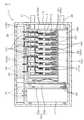
本例の電力変換装置1は、図1〜図3に示すごとく、複数の半導体モジュール2と複数の冷媒流路11(冷却管110)とを積層した積層体10と、複数のバスバー3と、コンデンサ4と、入力端子台12とを備える。
半導体モジュール2は、半導体素子を内蔵した本体部21と、該本体部21から突出したパワー端子20を有する。冷媒流路11には、半導体モジュール2を冷却する冷媒18が流れる。Example 1
The Example which concerns on the said power converter device is described using FIGS.
As shown in FIGS. 1 to 3, the
The
バスバー3は、半導体モジュール2のパワー端子20に接続している。図2に示すごとく、複数のバスバー3には、直流電源7(図6参照)の正電極に接続される正極バスバー3aと、直流電源7の負電極に接続される負極バスバー3bと、交流負荷70(図6参照)に接続される交流バスバー3cとがある。
コンデンサ4は、正極バスバー3aおよび負極バスバー3bにそれぞれ接続した一対のバスバー接続端子40(図5参照)と、直流電源7に接続される一対の入力端子41(図1参照)とを有する。コンデンサ4は、正極バスバー3aと負極バスバー3bとの間に加わる直流電圧を平滑化する。The
図1に示すごとく、入力端子台12には、コンデンサ4の入力端子41が載置される。
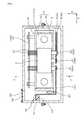
コンデンサ4は、積層体10に対して、積層体10の積層方向(X方向)に隣接する位置に配されている。
図3、図7に示すごとく、入力端子台12は、パワー端子20の突出方向(Z方向)における、パワー端子20を設けた側とは反対側の、コンデンサ4の端部45付近に設けられている。As shown in FIG. 1, the
The
As shown in FIGS. 3 and 7, the
図7に示すごとく、入力端子41は、コンデンサ4の上記端部45付近から、Y方向に突出している。入力端子41には、Z方向に貫通した貫通孔410が形成されている。また、入力端子台12にはナット120がインサートされている。上記直流電源7の接続端子(図示しない)を入力端子41に重ね合わせ、ボルトを貫通孔410に挿入し、ナット120に螺合することにより、直流電源7の接続端子と入力端子41とを締結するようになっている。 As shown in FIG. 7, the
図2に示すごとく、半導体モジュール2は、複数のパワー端子20と、制御端子22とを有する。複数のパワー端子20には、正極バスバー3aが接続する正極端子20aと、負極バスバー3bが接続する負極端子20bと、交流バスバー3cが接続する交流端子20cとがある。また、制御端子22には、制御回路基板14が接続している。制御回路基板14に形成した制御回路140が、半導体モジュール2のスイッチング動作を制御することにより、正極端子20aと負極端子20bとの間に印加される直流電圧を交流電圧に変換し、交流端子20cから出力するようになっている。 As shown in FIG. 2, the
図5に示すごとく、電力変換装置1は、6個の交流バスバー3cを有する。これら6個の交流バスバー3cの端子30は、それぞれ3個ずつのセットになって、出力端子台13に載置されている。2個の出力端子台13(13a,13b)には、それぞれ別の交流負荷70(図6参照)の接続端子が取り付けられる。 As shown in FIG. 5, the
また、図1に示すごとく、複数の冷却管110は、連結管15によって互いに連結されている。複数の冷却管110のうち、X方向における一端に位置する冷却管110aには、積層体10に冷媒18を導入するための導入パイプ16と、冷媒18を導出するための導出パイプ17とが取り付けられている。導入パイプ16から冷媒18を導入すると、冷媒18は連結管15を通って全ての冷却管110を流れ、導出パイプ17から導出する。これにより、半導体モジュール2を冷却するようになっている。 Further, as shown in FIG. 1, the plurality of cooling
積層体10は、平面視が略矩形状を呈する金属製のフレーム5内に固定されている。フレーム5の、X方向に直交する二つの壁部50a,50bのうち、一方の壁部50aと、積層体10との間には、弾性部材19(板ばね)が介在している。この弾性部材19によって、積層体10を他方の壁部50bに向けて押圧し、固定している。 The laminate 10 is fixed in a
なお、本例では、フレーム5の一方の壁部50aと積層体10との間に弾性部材19を配置したが、他方の壁部50b(パイプ16,17を設けた側の壁部)と積層体10との間に弾性部材19を配置してもよい。この場合には、積層体10は一方の壁部50aに向けて押圧されることになる。 In this example, the
また、本例の電力変換装置1は、フレーム5(積層体10)と、コンデンサ4と、入力端子台12と、出力端子台13とを収納する収納ケース6を備える。収納ケース6の内面66から、冷却管110の長手方向(Y方向)に向って、フレーム固定梁61(図4参照)とコンデンサ固定梁62とが延出している。フレーム固定梁61とコンデンサ固定梁62は、それぞれフレーム5とコンデンサ4との間に介在している。 The
図3に示すごとく、フレーム5は、X方向における両端部から、それぞれX方向に突出したリブ部51,52を有する。また、コンデンサ4は、X方向における両端部から、それぞれX方向に突出したコンデンサリブ部46,47を有する。フレーム5の、X方向における一方側に設けたリブ部51は、収納ケース6にボルト固定されている。また、フレーム5の、X方向における他方側に設けたリブ部52は、フレーム固定梁61にボルト固定されている。
コンデンサ4の、X方向における一方側に設けたコンデンサリブ部46は、コンデンサ固定梁62にボルト固定されている。また、X方向における他方側に設けたコンデンサリブ部47は、収納ケース6にボルト固定されている。As shown in FIG. 3, the
A
フレーム固定梁61とコンデンサ固定梁62とは、一本の共通梁60によって構成されている。フレーム固定梁61とコンデンサ固定梁62は、それぞれ板状に形成されている。フレーム固定梁61の法線方向はZ方向に平行であり、コンデンサ固定梁62の法線方向はX方向に平行である。共通梁60は、断面形状が略L字状を呈する。 The
フレーム固定梁61と、上記リブ部52とには、Z方向に貫通したボルト挿通孔がそれぞれ形成されている。このボルト挿通孔にボルト520を挿入し、袋ナット610に螺合することにより、リブ部52をフレーム固定梁61に固定するようになっている。また、フレーム5の、X方向における一方側に設けたリブ部51も同様に、ボルト520によって収納ケース6に固定されている。 Bolt insertion holes penetrating in the Z direction are formed in the
コンデンサ固定梁62の、Z方向における、制御回路基板14を配置した側とは反対側の端部625には、雌螺子部620が形成されている。また、コンデンサ4の上記コンデンサリブ部46には、Z方向に貫通したボルト挿通孔が形成されている。このボルト挿通孔にボルト530を挿入し、雌螺子部620に螺合することにより、コンデンサリブ部46をコンデンサ固定梁62に固定している。また、コンデンサ4の、X方向における他方側に設けたコンデンサリブ部47も同様に、ボルト530によって収納ケース6に固定されている。 A
また、図1に示すごとく、本例の電力変換装置1は、収納ケース6の内面66から積層方向(X方向)に延出した積層方向延出梁63を備える。積層方向延出梁63は、収納ケース6を、積層体10およびコンデンサ4を収納する第1部分S1(図4参照)と、入力端子台12および出力端子台13を収納する第2部分S2とに区画している。共通梁60の、Y方向における一方の端部651は収納ケース6に接続し、他方の端部652は積層方向延出梁63に接続している。 As shown in FIG. 1, the
図3に示すごとく、収納ケース6は、第1部分6aと第2部分6bとの2つの部分をボルト締結してなる。収納ケース6の第1部分6aには、Z方向に貫通した開口部68と、Y方向に貫通した3個の端子挿入穴67(67a〜67c;図1参照)が形成されている。入力端子台12及び出力端子台13は、開口部68および端子挿入穴67付近に設けられている。 As shown in FIG. 3, the
電力変換装置1と直流電源7(図6参照)とを電気的に接続する際には、直流電源7の接続端子(図示しない)を端子挿入穴67aに差し込み、収納ケース6の開口部68からボルトを挿入して、接続端子と入力端子41とを締結する。同様に、電力変換装置1と交流負荷70(図6参照)とを電気的に接続する際には、交流負荷70の接続端子を端子挿入穴67b、67cから差し込み、開口部68からボルトを挿入して、交流バスバー3cの端子30と上記接続端子とを締結する。これらの締結作業が完了した後、開口部68にカバー69を取り付ける。 When the
一方、図5に示すごとく、負極バスバー3bは、金属板からなる板状本体部350と、該板状本体部350に設けられた櫛歯状部351とを有する。この櫛歯状部351が、半導体モジュール2の負極端子20bに接続している。正極バスバー3aも同様の構造になっている。正極バスバー3aと負極バスバー3bは、コンデンサ4のバスバー接続端子40に接続している。 On the other hand, as shown in FIG. 5, the negative
次に、電力変換装置1の電気回路の説明をする。図6に示すごとく、本例の電力変換装置1は、9個の半導体モジュール2を備える。個々の半導体モジュール2は、2個の半導体素子23(IGBT素子)と、該半導体素子23に逆並列接続したフリーホイールダイオード24とを備える。半導体素子23には、正極バスバー3aに接続した上アーム半導体素子23aと、負極バスバー3bに接続した下アーム半導体素子23bとがある。上アーム半導体素子23aのコレクタ端子は、上述した正極端子20aとなっている。また、下アーム半導体素子23bのエミッタ端子は、負極端子20bとなっている。上アーム半導体素子23aのエミッタ端子と、下アーム半導体素子23bのコレクタ端子とは、それぞれ交流端子20cに接続している。正極端子20aは、正極バスバー3aを介して直流電源7の正電極に接続しており、負極端子20bは、負極バスバー3bを介して直流電源7の負電極に接続している。また、交流端子20cは、交流バスバー3cを介して交流負荷70(三相交流モータ)に接続している。 Next, the electric circuit of the
本例の作用効果について説明する。本例では図3に示すごとく、コンデンサ4を、積層体10に対してX方向に隣接する位置に配置してある。
このようにすると、従来の電力変換装置9(図11参照)のようにコンデンサ4と積層体10とがZ方向に隣接しなくなり、電力変換装置1の、Z方向における長さを短くすることができる。そのため、電力変換装置1の周辺に配された他の機器との関係で、Z方向における電力変換装置1の長さを短くすることが要求されている場合に有効である。The effect of this example will be described. In this example, as shown in FIG. 3, the
If it does in this way, like the conventional power converter device 9 (refer to Drawing 11),
また、本例では、入力端子台12を、Z方向における、パワー端子20を設けた側とは反対側の、コンデンサ4の端部45付近に設けてある。つまり、コンデンサ4の近くに入力端子台12を配置してある。そのため、コンデンサ4の入力端子41を短くすることができる。これにより、従来の電力変換装置1のように長い接続部材99(図9参照)を用いる必要がなくなり、電力変換装置1の製造コストを低減することが可能となる。また、接続部材99が不要となるため、電力変換装置1を小型化しやすくなる。 In this example, the
また、図1、図3に示すごとく、本例の電力変換装置1は、フレーム固定梁61およびコンデンサ固定梁62を備える。そして、フレーム5をフレーム固定梁61に固定し、コンデンサ4をコンデンサ固定梁62に固定してある。
このようにすると、フレーム5およびコンデンサ4の、X方向における両端部(リブ部51,52およびコンデンサリブ部46,47)を固定できるようになる。これにより、フレーム5およびコンデンサ4をしっかりと固定でき、電力変換装置1の耐振性を高めることが可能になる。As shown in FIGS. 1 and 3, the
If it does in this way, both ends (
また、本例の電力変換装置1は、ハイブリッド車や電気自動車等の車両に搭載される。車両が走行すると振動が発生するため、車両用の電力変換装置1には特に高い耐振性が要求されている。本例の電力変換装置1は、上述したように高い耐振性を備えるため、車両の走行時に大きな振動が発生しても、充分に耐えることができる。 The
また、本例では図1、図3に示すごとく、フレーム固定梁61とコンデンサ固定梁62とが一本の共通梁60によって構成されている。
このようにすると、フレーム固定梁61とコンデンサ固定梁62とを共通化できるため、これらの固定梁61,62を構成する材料(金属材料)の使用量を低減できる。これにより、電力変換装置1の製造コストを低減でき、電力変換装置1を軽量化することが可能になる。In this example, as shown in FIGS. 1 and 3, the
In this way, since the
また、本例では図1に示すごとく、上記積層方向延出梁63を備える。そして、共通梁60は、Y方向における一方の端部651が収納ケース6に接続し、他方の端部652が積層方向延出梁63に接続している。
このようにすると、共通梁60の他方の端部652を積層方向延出梁63に接続してあるので、共通梁60の他方の端部652を入力端子台12や出力端子台13の付近まで延出させなくてすむ。そのため、共通梁60が入力端子台12や出力端子台13と干渉することを防止できる。
また、上記構成にすると、共通梁60の一方の端部651を収納ケース6に固定でき、他方の端部652を積層方向延出梁63に固定できるため、共通梁60の両端を固定でき、耐振性をより高めることが可能になる。In this example, as shown in FIG. 1, the stacking
In this way, the
Further, with the above configuration, since one
以上のごとく、本例によれば、小型化しやすく、製造コストを低減できる電力変換装置を提供することができる。 As described above, according to this example, it is possible to provide a power conversion device that can be easily miniaturized and can reduce manufacturing costs.
なお、本例では、冷媒流路11を内部に有する複数の冷却管110と、複数の半導体モジュール2とを積層して積層体10を構成したが、図8に示すごとく、半導体素子を内蔵した本体部21と枠体28とを一体に備えた冷却器一体型半導体モジュール29を積層することにより、半導体モジュール2と冷媒流路11とが積層される構造にしてもよい。冷却器一体型半導体モジュール29の枠体28は、本体部21よりもX方向における幅が大きい。また、枠体28と本体部21との間には空間が設けられている。この空間が、冷媒流路11となる。 In addition, in this example, although the
(実施例2)
本例は図9に示すごとく、入力端子台12を、コンデンサ4に対してX方向に隣接する位置に配置した例である。本例では、コンデンサ4の入力端子41は、X方向における積層体10を設けた側とは反対側に突出している。そして、この入力端子41を、入力端子台12に載置してある。
このようにすると、電力変換装置1の周囲に配置された他の機器との関係で、入力端子台12を、コンデンサ4に対してY方向に隣接する位置に配置できない場合等に有効である。
その他、実施例1と同様の構成および作用効果を有する。(Example 2)
In this example, as shown in FIG. 9, the
This is effective when the
In addition, the configuration and operational effects are the same as those of the first embodiment.
(実施例3)
本例は、図10に示すごとく、コンデンサ4の入力端子41の形状を変更した例である。本例のコンデンサ4は、第1入力端子41aと第2入力端子41bとの2つの入力端子41を有する。第1入力端子41aは、コンデンサ4の端部45に対して、Z方向に少し離れた位置に設けられている。(Example 3)
In this example, as shown in FIG. 10, the shape of the
第2入力端子41bは、端子台12に形成された保持爪(図示しない)によって、端子台12に固定されている。第1入力端子41aと第2入力端子41bとは、締結部材415によって互いに締結されている。 The
第2入力端子41bは、第1入力端子41aに接続する第1部分411と、該第1部分411からZ方向に延びる第2部分412と、該第2部分412からY方向に延びる第3部分413とを備える。この第3部分413が、端子台12に載置されている。
その他、実施例1と同様の構成を備える。The
In addition, the same configuration as that of the first embodiment is provided.
本例の作用効果について説明する。上記構成にすると、コンデンサ4の第1入力端子41aを、上記端部45から離れた位置に形成することができるため、コンデンサ4の設計自由度を高めることができる。なお、第2入力端子41bのZ方向における長さは、短くすることが好ましい。あまり長くすると、第2入力端子41bを構成する金属材料の量が増え、第2入力端子41bの製造コストが上昇したり、電気抵抗が増加して発熱量が増える等の問題が発生するからである。
その他、実施例1と同様の作用効果を有する。The effect of this example will be described. With the above configuration, the
In addition, the same effects as those of the first embodiment are obtained.
1 電力変換装置
10 積層体
11 冷媒流路
12 入力端子台
13 出力端子台
2 半導体モジュール
3 バスバー
3a 正極バスバー
3b 負極バスバー
3c 交流バスバー
4 コンデンサ
41 入力端子DESCRIPTION OF
Claims (4)
Translated fromJapanese上記パワー端子に接続した複数のバスバーとを備えた電力変換装置であって、
上記複数のバスバーには、直流電源の正電極に接続される正極バスバーと、上記直流電源の負電極に接続される負極バスバーと、交流負荷に接続される交流バスバーとがあり、
上記正極バスバーおよび上記負極バスバーにそれぞれ接続した一対のバスバー接続端子と、上記直流電源に接続される一対の入力端子とを有し、上記正極バスバーと上記負極バスバーとの間に加わる直流電圧を平滑化するコンデンサと、
上記入力端子を載置する入力端子台とを備え、
上記コンデンサは、上記積層体に対して、該積層体の積層方向に隣接する位置に配されており、
上記入力端子台は、上記パワー端子の突出方向における、上記パワー端子を設けた側とは反対側の、上記コンデンサの端部付近に設けられていることを特徴とする電力変換装置。A laminated body in which a plurality of semiconductor modules in which power terminals protrude from a main body portion incorporating a semiconductor element, and a plurality of refrigerant flow paths through which a refrigerant for cooling the semiconductor modules flows;
A power conversion device comprising a plurality of bus bars connected to the power terminal,
The plurality of bus bars include a positive bus bar connected to a positive electrode of a DC power source, a negative bus bar connected to a negative electrode of the DC power source, and an AC bus bar connected to an AC load.
A pair of bus bar connection terminals respectively connected to the positive electrode bus bar and the negative electrode bus bar, and a pair of input terminals connected to the DC power source, and smoothes the DC voltage applied between the positive electrode bus bar and the negative electrode bus bar. A capacitor
An input terminal block on which the input terminal is placed;
The capacitor is disposed at a position adjacent to the stacked body in the stacking direction of the stacked body,
The power conversion device according to claim 1, wherein the input terminal block is provided near an end portion of the capacitor on a side opposite to a side where the power terminal is provided in a protruding direction of the power terminal.
Priority Applications (3)
| Application Number | Priority Date | Filing Date | Title |
|---|---|---|---|
| JP2011193677AJP5344013B2 (en) | 2011-09-06 | 2011-09-06 | Power converter |
| CN201210326560.7ACN103078534B (en) | 2011-09-06 | 2012-09-05 | Power converter permitted to be reduced in size and manufactured at decreased cost |
| US13/603,527US8792244B2 (en) | 2011-09-06 | 2012-09-05 | Power converter permitted to be reduced in size and manufactured at decreased cost |
Applications Claiming Priority (1)
| Application Number | Priority Date | Filing Date | Title |
|---|---|---|---|
| JP2011193677AJP5344013B2 (en) | 2011-09-06 | 2011-09-06 | Power converter |
Publications (2)
| Publication Number | Publication Date |
|---|---|
| JP2013055840A JP2013055840A (en) | 2013-03-21 |
| JP5344013B2true JP5344013B2 (en) | 2013-11-20 |
Family
ID=47753053
Family Applications (1)
| Application Number | Title | Priority Date | Filing Date |
|---|---|---|---|
| JP2011193677AActiveJP5344013B2 (en) | 2011-09-06 | 2011-09-06 | Power converter |
Country Status (3)
| Country | Link |
|---|---|
| US (1) | US8792244B2 (en) |
| JP (1) | JP5344013B2 (en) |
| CN (1) | CN103078534B (en) |
Families Citing this family (39)
| Publication number | Priority date | Publication date | Assignee | Title |
|---|---|---|---|---|
| JP2014078599A (en)* | 2012-10-10 | 2014-05-01 | Denso Corp | Power conversion device |
| JP5700022B2 (en) | 2012-10-29 | 2015-04-15 | 株式会社デンソー | Power converter |
| JP5655846B2 (en)* | 2012-12-04 | 2015-01-21 | 株式会社デンソー | Power converter |
| CN104981901B (en)* | 2012-12-07 | 2018-05-15 | Abb 技术有限公司 | Semiconductor subassembly |
| DE112014001321T5 (en)* | 2013-03-14 | 2016-01-14 | Yazaki Corporation | Electronic component assembly structure and electrical connection box |
| JP5821890B2 (en)* | 2013-04-17 | 2015-11-24 | トヨタ自動車株式会社 | Power converter |
| JP5747943B2 (en)* | 2013-05-30 | 2015-07-15 | 株式会社デンソー | Power converter |
| JP6135319B2 (en)* | 2013-06-14 | 2017-05-31 | 株式会社デンソー | Power converter |
| US9226431B2 (en)* | 2013-12-18 | 2015-12-29 | Caterpillar Inc. | Cast housing for a configurable power converter |
| JP6044559B2 (en) | 2014-02-05 | 2016-12-14 | 株式会社デンソー | Power converter |
| JP6331866B2 (en)* | 2014-08-18 | 2018-05-30 | 株式会社デンソー | Power converter |
| JP6375784B2 (en)* | 2014-08-29 | 2018-08-22 | 株式会社デンソー | Power converter |
| JP2016063641A (en)* | 2014-09-18 | 2016-04-25 | 株式会社デンソー | Power converter |
| JP6303961B2 (en)* | 2014-09-30 | 2018-04-04 | 株式会社デンソー | Power converter |
| JP6394262B2 (en) | 2014-10-14 | 2018-09-26 | 株式会社デンソー | Power converter |
| US9756755B2 (en)* | 2014-10-31 | 2017-09-05 | Denso Corporation | Electric power converter |
| JP6428252B2 (en)* | 2014-12-23 | 2018-11-28 | 株式会社デンソー | Power converter |
| JP6187448B2 (en)* | 2014-12-24 | 2017-08-30 | トヨタ自動車株式会社 | Laminated unit |
| JP6398800B2 (en) | 2015-03-06 | 2018-10-03 | 株式会社デンソー | Power converter |
| JP6459904B2 (en)* | 2015-11-02 | 2019-01-30 | 株式会社デンソー | Power converter |
| JP6488991B2 (en) | 2015-11-17 | 2019-03-27 | 株式会社デンソー | Power converter |
| JP6500756B2 (en) | 2015-11-17 | 2019-04-17 | 株式会社デンソー | Power converter |
| JP6583072B2 (en)* | 2016-03-15 | 2019-10-02 | 住友電気工業株式会社 | Semiconductor module |
| JP6583137B2 (en)* | 2016-05-19 | 2019-10-02 | 株式会社デンソー | Power converter |
| US10955202B2 (en)* | 2016-06-30 | 2021-03-23 | Advanced Thermal Solutions, Inc. | Cold plate heat exchanger |
| JP6596398B2 (en)* | 2016-08-29 | 2019-10-23 | 本田技研工業株式会社 | Power converter |
| JP6229776B2 (en)* | 2016-09-05 | 2017-11-15 | 株式会社デンソー | Power converter |
| US10136564B2 (en)* | 2016-09-30 | 2018-11-20 | Denso Corporation | Power converter |
| JP6758571B2 (en)* | 2016-12-13 | 2020-09-23 | 株式会社デンソー | Power converter |
| JP6784197B2 (en)* | 2017-03-09 | 2020-11-11 | 株式会社デンソー | Power converter |
| JP2019180113A (en)* | 2018-03-30 | 2019-10-17 | 本田技研工業株式会社 | Power conversion device |
| JP6717347B2 (en)* | 2018-07-25 | 2020-07-01 | 株式会社デンソー | Power converter |
| JP6583513B2 (en)* | 2018-11-01 | 2019-10-02 | 株式会社デンソー | Power converter |
| US11855528B2 (en) | 2018-12-26 | 2023-12-26 | Panasonic Intellectual Property Management Co., Ltd. | Power conversion apparatus |
| JP6769535B2 (en)* | 2019-09-05 | 2020-10-14 | 株式会社デンソー | Power converter |
| JP7156319B2 (en)* | 2020-01-22 | 2022-10-19 | 株式会社デンソー | power converter |
| US11502349B2 (en) | 2020-08-31 | 2022-11-15 | Borgwarner, Inc. | Cooling manifold assembly |
| JP7318615B2 (en)* | 2020-09-11 | 2023-08-01 | トヨタ自動車株式会社 | power converter |
| CN119673666B (en)* | 2025-02-14 | 2025-07-15 | 宁波新容电器科技有限公司 | Water-cooled built-in integrated capacitor |
Family Cites Families (13)
| Publication number | Priority date | Publication date | Assignee | Title |
|---|---|---|---|---|
| DE10058574B4 (en)* | 2000-11-24 | 2005-09-15 | Danfoss Drives A/S | Cooling unit for power semiconductors |
| JP4452605B2 (en)* | 2004-11-10 | 2010-04-21 | トヨタ自動車株式会社 | Semiconductor device |
| US7233494B2 (en)* | 2005-05-06 | 2007-06-19 | International Business Machines Corporation | Cooling apparatus, cooled electronic module and methods of fabrication thereof employing an integrated manifold and a plurality of thermally conductive fins |
| JP4848187B2 (en)* | 2006-01-17 | 2011-12-28 | 日立オートモティブシステムズ株式会社 | Power converter |
| JP4770490B2 (en)* | 2006-01-31 | 2011-09-14 | トヨタ自動車株式会社 | Power semiconductor element cooling structure and inverter |
| JP2007312545A (en)* | 2006-05-19 | 2007-11-29 | Fuji Electric Fa Components & Systems Co Ltd | Inverter casing structure and manufacturing method thereof |
| JP4442593B2 (en)* | 2006-07-20 | 2010-03-31 | 株式会社日立製作所 | Power converter |
| JP4905254B2 (en)* | 2007-05-25 | 2012-03-28 | トヨタ自動車株式会社 | Manufacturing method of bus bar with integrated capacitor |
| JP4452952B2 (en) | 2007-06-20 | 2010-04-21 | 日立オートモティブシステムズ株式会社 | Power converter |
| US7616442B1 (en)* | 2008-04-25 | 2009-11-10 | Rockwell Automation Technologies, Inc. | Power electronic module cooling system and method |
| JP5120221B2 (en)* | 2008-11-17 | 2013-01-16 | 株式会社デンソー | Power converter |
| JP5429151B2 (en)* | 2010-01-14 | 2014-02-26 | 株式会社デンソー | Power converter |
| JP5471567B2 (en)* | 2010-02-17 | 2014-04-16 | 株式会社デンソー | Power converter |
- 2011
- 2011-09-06JPJP2011193677Apatent/JP5344013B2/enactiveActive
- 2012
- 2012-09-05USUS13/603,527patent/US8792244B2/enactiveActive
- 2012-09-05CNCN201210326560.7Apatent/CN103078534B/enactiveActive
Also Published As
| Publication number | Publication date |
|---|---|
| US20130058068A1 (en) | 2013-03-07 |
| JP2013055840A (en) | 2013-03-21 |
| US8792244B2 (en) | 2014-07-29 |
| CN103078534B (en) | 2015-05-27 |
| CN103078534A (en) | 2013-05-01 |
Similar Documents
| Publication | Publication Date | Title |
|---|---|---|
| JP5344013B2 (en) | Power converter | |
| JP5799843B2 (en) | Power converter | |
| JP5344012B2 (en) | Power converter | |
| JP5655846B2 (en) | Power converter | |
| JP5505398B2 (en) | Power converter | |
| JP5760985B2 (en) | Power converter | |
| JP5621741B2 (en) | Power converter | |
| JP5531992B2 (en) | Power converter | |
| JP2014090629A (en) | Power conversion device | |
| JP6232315B2 (en) | Power converter | |
| JP5343928B2 (en) | Power converter | |
| JP5949273B2 (en) | Power converter | |
| JP5505080B2 (en) | Power converter | |
| JP2014057400A (en) | Electric power conversion apparatus | |
| JP2013099168A (en) | Power conversion device | |
| JP5978885B2 (en) | Power converter | |
| JP2013074722A (en) | Power conversion device | |
| JP6115430B2 (en) | Power converter | |
| JP5760995B2 (en) | Power converter | |
| JP5445446B2 (en) | Power converter | |
| JP2016149911A (en) | Power converter | |
| JP2018182075A (en) | Capacitor module | |
| JP5994717B2 (en) | Power converter | |
| JP5928269B2 (en) | Power converter | |
| JP5526843B2 (en) | Power converter |
Legal Events
| Date | Code | Title | Description |
|---|---|---|---|
| A621 | Written request for application examination | Free format text:JAPANESE INTERMEDIATE CODE: A621 Effective date:20121225 | |
| A977 | Report on retrieval | Free format text:JAPANESE INTERMEDIATE CODE: A971007 Effective date:20130708 | |
| TRDD | Decision of grant or rejection written | ||
| A01 | Written decision to grant a patent or to grant a registration (utility model) | Free format text:JAPANESE INTERMEDIATE CODE: A01 Effective date:20130716 | |
| A61 | First payment of annual fees (during grant procedure) | Free format text:JAPANESE INTERMEDIATE CODE: A61 Effective date:20130729 | |
| R151 | Written notification of patent or utility model registration | Ref document number:5344013 Country of ref document:JP Free format text:JAPANESE INTERMEDIATE CODE: R151 | |
| R250 | Receipt of annual fees | Free format text:JAPANESE INTERMEDIATE CODE: R250 | |
| R250 | Receipt of annual fees | Free format text:JAPANESE INTERMEDIATE CODE: R250 | |
| R250 | Receipt of annual fees | Free format text:JAPANESE INTERMEDIATE CODE: R250 | |
| R250 | Receipt of annual fees | Free format text:JAPANESE INTERMEDIATE CODE: R250 | |
| R250 | Receipt of annual fees | Free format text:JAPANESE INTERMEDIATE CODE: R250 | |
| R250 | Receipt of annual fees | Free format text:JAPANESE INTERMEDIATE CODE: R250 | |
| R250 | Receipt of annual fees | Free format text:JAPANESE INTERMEDIATE CODE: R250 | |
| R250 | Receipt of annual fees | Free format text:JAPANESE INTERMEDIATE CODE: R250 | |
| R250 | Receipt of annual fees | Free format text:JAPANESE INTERMEDIATE CODE: R250 | |
| R250 | Receipt of annual fees | Free format text:JAPANESE INTERMEDIATE CODE: R250 |