JP5340806B2 - Laser processing method of semiconductor wafer - Google Patents
Laser processing method of semiconductor waferDownload PDFInfo
- Publication number
- JP5340806B2 JP5340806B2JP2009123434AJP2009123434AJP5340806B2JP 5340806 B2JP5340806 B2JP 5340806B2JP 2009123434 AJP2009123434 AJP 2009123434AJP 2009123434 AJP2009123434 AJP 2009123434AJP 5340806 B2JP5340806 B2JP 5340806B2
- Authority
- JP
- Japan
- Prior art keywords
- semiconductor wafer
- laser processing
- laser
- laser beam
- pulse width
- Prior art date
- Legal status (The legal status is an assumption and is not a legal conclusion. Google has not performed a legal analysis and makes no representation as to the accuracy of the status listed.)
- Active
Links
Images


Classifications
- H—ELECTRICITY
- H01—ELECTRIC ELEMENTS
- H01L—SEMICONDUCTOR DEVICES NOT COVERED BY CLASS H10
- H01L21/00—Processes or apparatus adapted for the manufacture or treatment of semiconductor or solid state devices or of parts thereof
- H01L21/70—Manufacture or treatment of devices consisting of a plurality of solid state components formed in or on a common substrate or of parts thereof; Manufacture of integrated circuit devices or of parts thereof
- H01L21/77—Manufacture or treatment of devices consisting of a plurality of solid state components or integrated circuits formed in, or on, a common substrate
- H01L21/78—Manufacture or treatment of devices consisting of a plurality of solid state components or integrated circuits formed in, or on, a common substrate with subsequent division of the substrate into plural individual devices
- B—PERFORMING OPERATIONS; TRANSPORTING
- B23—MACHINE TOOLS; METAL-WORKING NOT OTHERWISE PROVIDED FOR
- B23K—SOLDERING OR UNSOLDERING; WELDING; CLADDING OR PLATING BY SOLDERING OR WELDING; CUTTING BY APPLYING HEAT LOCALLY, e.g. FLAME CUTTING; WORKING BY LASER BEAM
- B23K26/00—Working by laser beam, e.g. welding, cutting or boring
- B23K26/0006—Working by laser beam, e.g. welding, cutting or boring taking account of the properties of the material involved
- B—PERFORMING OPERATIONS; TRANSPORTING
- B23—MACHINE TOOLS; METAL-WORKING NOT OTHERWISE PROVIDED FOR
- B23K—SOLDERING OR UNSOLDERING; WELDING; CLADDING OR PLATING BY SOLDERING OR WELDING; CUTTING BY APPLYING HEAT LOCALLY, e.g. FLAME CUTTING; WORKING BY LASER BEAM
- B23K26/00—Working by laser beam, e.g. welding, cutting or boring
- B23K26/02—Positioning or observing the workpiece, e.g. with respect to the point of impact; Aligning, aiming or focusing the laser beam
- B23K26/06—Shaping the laser beam, e.g. by masks or multi-focusing
- B23K26/062—Shaping the laser beam, e.g. by masks or multi-focusing by direct control of the laser beam
- B23K26/0626—Energy control of the laser beam
- B—PERFORMING OPERATIONS; TRANSPORTING
- B23—MACHINE TOOLS; METAL-WORKING NOT OTHERWISE PROVIDED FOR
- B23K—SOLDERING OR UNSOLDERING; WELDING; CLADDING OR PLATING BY SOLDERING OR WELDING; CUTTING BY APPLYING HEAT LOCALLY, e.g. FLAME CUTTING; WORKING BY LASER BEAM
- B23K26/00—Working by laser beam, e.g. welding, cutting or boring
- B23K26/36—Removing material
- B23K26/40—Removing material taking account of the properties of the material involved
- H—ELECTRICITY
- H01—ELECTRIC ELEMENTS
- H01L—SEMICONDUCTOR DEVICES NOT COVERED BY CLASS H10
- H01L21/00—Processes or apparatus adapted for the manufacture or treatment of semiconductor or solid state devices or of parts thereof
- H01L21/67—Apparatus specially adapted for handling semiconductor or electric solid state devices during manufacture or treatment thereof; Apparatus specially adapted for handling wafers during manufacture or treatment of semiconductor or electric solid state devices or components ; Apparatus not specifically provided for elsewhere
- H01L21/67005—Apparatus not specifically provided for elsewhere
- H01L21/67011—Apparatus for manufacture or treatment
- H01L21/67132—Apparatus for placing on an insulating substrate, e.g. tape
- H—ELECTRICITY
- H01—ELECTRIC ELEMENTS
- H01L—SEMICONDUCTOR DEVICES NOT COVERED BY CLASS H10
- H01L21/00—Processes or apparatus adapted for the manufacture or treatment of semiconductor or solid state devices or of parts thereof
- H01L21/67—Apparatus specially adapted for handling semiconductor or electric solid state devices during manufacture or treatment thereof; Apparatus specially adapted for handling wafers during manufacture or treatment of semiconductor or electric solid state devices or components ; Apparatus not specifically provided for elsewhere
- H01L21/683—Apparatus specially adapted for handling semiconductor or electric solid state devices during manufacture or treatment thereof; Apparatus specially adapted for handling wafers during manufacture or treatment of semiconductor or electric solid state devices or components ; Apparatus not specifically provided for elsewhere for supporting or gripping
- H01L21/6835—Apparatus specially adapted for handling semiconductor or electric solid state devices during manufacture or treatment thereof; Apparatus specially adapted for handling wafers during manufacture or treatment of semiconductor or electric solid state devices or components ; Apparatus not specifically provided for elsewhere for supporting or gripping using temporarily an auxiliary support
- H01L21/6836—Wafer tapes, e.g. grinding or dicing support tapes
- B—PERFORMING OPERATIONS; TRANSPORTING
- B23—MACHINE TOOLS; METAL-WORKING NOT OTHERWISE PROVIDED FOR
- B23K—SOLDERING OR UNSOLDERING; WELDING; CLADDING OR PLATING BY SOLDERING OR WELDING; CUTTING BY APPLYING HEAT LOCALLY, e.g. FLAME CUTTING; WORKING BY LASER BEAM
- B23K2103/00—Materials to be soldered, welded or cut
- B23K2103/50—Inorganic material, e.g. metals, not provided for in B23K2103/02 – B23K2103/26
- B23K2103/56—Inorganic material, e.g. metals, not provided for in B23K2103/02 – B23K2103/26 semiconducting
- H—ELECTRICITY
- H01—ELECTRIC ELEMENTS
- H01L—SEMICONDUCTOR DEVICES NOT COVERED BY CLASS H10
- H01L21/00—Processes or apparatus adapted for the manufacture or treatment of semiconductor or solid state devices or of parts thereof
- H01L21/67—Apparatus specially adapted for handling semiconductor or electric solid state devices during manufacture or treatment thereof; Apparatus specially adapted for handling wafers during manufacture or treatment of semiconductor or electric solid state devices or components ; Apparatus not specifically provided for elsewhere
- H01L21/67005—Apparatus not specifically provided for elsewhere
- H01L21/67011—Apparatus for manufacture or treatment
- H01L21/67144—Apparatus for mounting on conductive members, e.g. leadframes or conductors on insulating substrates
- H—ELECTRICITY
- H01—ELECTRIC ELEMENTS
- H01L—SEMICONDUCTOR DEVICES NOT COVERED BY CLASS H10
- H01L2221/00—Processes or apparatus adapted for the manufacture or treatment of semiconductor or solid state devices or of parts thereof covered by H01L21/00
- H01L2221/67—Apparatus for handling semiconductor or electric solid state devices during manufacture or treatment thereof; Apparatus for handling wafers during manufacture or treatment of semiconductor or electric solid state devices or components; Apparatus not specifically provided for elsewhere
- H01L2221/683—Apparatus for handling semiconductor or electric solid state devices during manufacture or treatment thereof; Apparatus for handling wafers during manufacture or treatment of semiconductor or electric solid state devices or components; Apparatus not specifically provided for elsewhere for supporting or gripping
- H01L2221/68304—Apparatus for handling semiconductor or electric solid state devices during manufacture or treatment thereof; Apparatus for handling wafers during manufacture or treatment of semiconductor or electric solid state devices or components; Apparatus not specifically provided for elsewhere for supporting or gripping using temporarily an auxiliary support
- H01L2221/68327—Apparatus for handling semiconductor or electric solid state devices during manufacture or treatment thereof; Apparatus for handling wafers during manufacture or treatment of semiconductor or electric solid state devices or components; Apparatus not specifically provided for elsewhere for supporting or gripping using temporarily an auxiliary support used during dicing or grinding
- H01L2221/68336—Apparatus for handling semiconductor or electric solid state devices during manufacture or treatment thereof; Apparatus for handling wafers during manufacture or treatment of semiconductor or electric solid state devices or components; Apparatus not specifically provided for elsewhere for supporting or gripping using temporarily an auxiliary support used during dicing or grinding involving stretching of the auxiliary support post dicing
Landscapes
- Engineering & Computer Science (AREA)
- Physics & Mathematics (AREA)
- Optics & Photonics (AREA)
- General Physics & Mathematics (AREA)
- Mechanical Engineering (AREA)
- Condensed Matter Physics & Semiconductors (AREA)
- Plasma & Fusion (AREA)
- Manufacturing & Machinery (AREA)
- Computer Hardware Design (AREA)
- Microelectronics & Electronic Packaging (AREA)
- Power Engineering (AREA)
- Laser Beam Processing (AREA)
- Dicing (AREA)
Description
Translated fromJapanese本発明は、半導体ウエーハの分割予定ラインに沿ってレーザビームを照射して半導体ウエーハにレーザ加工溝を形成する半導体ウエーハの加工方法に関する。 The present invention relates to a semiconductor wafer processing method in which a laser processing groove is formed in a semiconductor wafer by irradiating a laser beam along a predetermined division line of the semiconductor wafer.
半導体デバイス製造プロセスにおいては、略円板形状であるシリコンウエーハ、ガリウム砒素ウエーハ等の半導体ウエーハの表面に格子状に形成されたストリートと呼ばれる分割予定ラインによって複数の領域が区画され、区画された各領域にIC、LSI等のデバイスを形成する。そして、半導体ウエーハは切削装置又はレーザ加工装置によって個々のデバイスに分割され、分割されたデバイスは携帯電話、パソコン等の各種電気機器に広く利用されている。 In the semiconductor device manufacturing process, a plurality of regions are defined by dividing lines called streets formed in a lattice shape on the surface of a semiconductor wafer such as a silicon wafer or a gallium arsenide wafer having a substantially disk shape. A device such as an IC or LSI is formed in the region. The semiconductor wafer is divided into individual devices by a cutting device or a laser processing device, and the divided devices are widely used in various electric devices such as mobile phones and personal computers.
切削装置としては一般にダイシング装置と呼ばれる切削装置が用いられており、この切削装置ではダイアモンドやCBN等の超砥粒をメタルやレジンで固めて厚さ30〜300μm程度とした切削ブレードが約30000rpmと高速回転しつつ半導体ウエーハへ切り込むことで切削が遂行される。 As a cutting device, a cutting device generally called a dicing device is used. In this cutting device, a cutting blade having a thickness of about 30 to 300 μm formed by hardening superabrasive grains such as diamond and CBN with metal or resin is about 30000 rpm. Cutting is performed by cutting into a semiconductor wafer while rotating at high speed.
一方、レーザ加工装置は、半導体ウエーハを保持するチャックテーブルと、該チャックテーブルに保持された半導体ウエーハにパルスレーザビームを照射するレーザビーム照射手段と、該チャックテーブルと該レーザビーム照射手段とを相対的に加工送りする加工送り手段とを少なくとも備えていて、半導体ウエーハの表面に形成された分割予定ラインに沿って半導体ウエーハに対して吸収性を有する波長のパルスレーザビームを照射してレーザ加工溝を形成し、次いで外力を付与してレーザ加工溝に沿って半導体ウエーハを破断して個々のデバイスに分割する(例えば、特開2007−19252号公報参照)。 On the other hand, the laser processing apparatus has a chuck table for holding a semiconductor wafer, a laser beam irradiation means for irradiating a semiconductor wafer held on the chuck table with a pulsed laser beam, and the chuck table and the laser beam irradiation means relative to each other. A laser processing groove by irradiating the semiconductor wafer with a pulsed laser beam having an absorptive wavelength along a predetermined division line formed on the surface of the semiconductor wafer. Then, an external force is applied, and the semiconductor wafer is broken along the laser processing groove to be divided into individual devices (see, for example, Japanese Patent Application Laid-Open No. 2007-19252).
しかし、切削ブレードを備えたダイシング装置によって半導体ウエーハを切削して形成したデバイスの抗折強度が800MPaであるのに対して、従来のレーザ加工方法によって形成したデバイスの抗折強度は400MPaと低く、電気機器の品質の低下を招くという問題がある。 However, the bending strength of a device formed by cutting a semiconductor wafer by a dicing apparatus equipped with a cutting blade is 800 MPa, whereas the bending strength of a device formed by a conventional laser processing method is as low as 400 MPa, There is a problem in that the quality of electrical equipment is degraded.
本発明はこのような点に鑑みてなされたものであり、その目的とするところは、抗折強度の高いデバイスを製造可能な半導体ウエーハのレーザ加工方法を提供することである。 The present invention has been made in view of these points, and an object of the present invention is to provide a laser processing method of a semiconductor wafer capable of manufacturing a device having high bending strength.
本発明によると、半導体ウエーハの加工方法であって、半導体ウエーハの分割予定ラインに沿って半導体ウエーハに対して吸収性を有する波長のパルスレーザビームを照射して半導体ウエーハにレーザ加工溝を形成する加工溝形成工程を具備し、該加工溝形成工程で照射されるパルスレーザビームのパルス幅が2ns以下であり、ピークエネルギー密度が5GW/cm2〜200GW/cm2であり、該加工溝形成工程では、半導体ウエーハに集光されるスポットがスポット径の16/20〜19/20の範囲内の重なり量でもって半導体ウエーハを加工送りして該加工溝を形成することを特徴とする半導体ウエーハのレーザ加工方法が提供される。According to the present invention, there is provided a method for processing a semiconductor wafer, wherein a laser processing groove is formed in a semiconductor wafer by irradiating the semiconductor wafer with a pulsed laser beam having an absorptivity with respect to the semiconductor wafer along a predetermined division line of the semiconductor wafer. comprising a groove forming step, the pulse width of the pulse laser beam irradiated in the groove forming step is not more 2ns or less,Ri peak energy density 5GW / cm2 ~200GW / cm2der, said groove forming In the process, the semiconductor wafer is formed by processing and feeding the semiconductor wafer with an overlapping amount of spots focused on the semiconductor wafer within a range of 16/20 to 19/20 of the spot diameter. A laser processing method is provided.
好ましくは、レーザービームのスポット径はφ5μm〜φ15μmの範囲内である。 Preferably, the spot diameter of the laser beam is in the range of φ5 μm to φ15 μm.
本発明によると、半導体ウエーハに対して吸収性を有する波長のパルスレーザビームのパルス幅を2ns以下に設定し、更にパルスレーザビームの1パルス当たりのピークエネルギー密度を5GW/cm2〜200GW/cm2に設定して半導体ウエーハにレーザ加工溝を形成するので、分割されたデバイスの抗折強度を800MPa以上にすることができる。According to the present invention, the pulse width of a pulse laser beam having a wavelength that is absorptive with respect to a semiconductor wafer is set to 2 ns or less, and the peak energy density per pulse of the pulse laser beam is set to 5 GW / cm2 to 200 GW / cm.Since the laser processing groove is formed in the semiconductor wafer by setting to2 , the bending strength of the divided device can be 800 MPa or more.
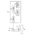
以下、本発明の実施形態を図面を参照して詳細に説明する。図1は、本発明の半導体ウエーハの加工方法を実施するのに適したレーザ加工装置の概略構成図を示している。 Hereinafter, embodiments of the present invention will be described in detail with reference to the drawings. FIG. 1 shows a schematic configuration diagram of a laser processing apparatus suitable for carrying out the semiconductor wafer processing method of the present invention.
レーザ加工装置2は、静止基台4上にX軸方向に移動可能に搭載された第1スライドブロック6を含んでいる。第1スライドブロック6は、ボールねじ8及びパルスモータ10から構成される加工送り手段12により一対のガイドレール14に沿って加工送り方向、すなわちX軸方向に移動される。 The
第1スライドブロック6上には第2スライドブロック16がY軸方向に移動可能に搭載されている。すなわち、第2スライドブロック16はボールねじ18及びパルスモータ20から構成される割り出し送り手段22により一対のガイドレール24に沿って割り出し方向、すなわちY軸方向に移動される。 A
第2スライドブロック16上には円筒支持部材26を介してチャックテーブル28が搭載されており、チャックテーブル28は加工送り手段12及び割り出し送り手段22によりX軸方向及びY軸方向に移動可能である。チャックテーブル28には、チャックテーブル28に吸引保持された半導体ウエーハをクランプするクランパ30が設けられている。 A chuck table 28 is mounted on the
静止基台4にはコラム32が立設されており、このコラム32にはレーザビーム照射ユニット34を収容するケーシング35が取り付けられている。レーザビーム照射ユニット34は、図3に示すように、YAGレーザ又はYVO4レーザを発振するレーザ発振器62と、繰り返し周波数設定手段64と、パルス幅調整手段66と、パワー調整手段68とを含んでいる。 A
レーザビーム照射ユニット34のパワー調整手段68により所定パワーに調整されたパルスレーザビームは、ケーシング35の先端に取り付けられた集光器36のミラー70で反射され、更に集光用対物レンズ72によって集光されてチャックテーブル28に保持されている半導体ウエーハWに照射される。 The pulse laser beam adjusted to a predetermined power by the power adjusting means 68 of the laser
ケーシング35の先端部には、集光器36とX軸方向に整列してレーザ加工すべき加工領域を検出する撮像手段38が配設されている。撮像手段38は、可視光によって半導体ウエーハの加工領域を撮像する通常のCCD等の撮像素子を含んでいる。 At the tip of the
撮像手段38は更に、半導体ウエーハに赤外線を照射する赤外線照射手段と、赤外線照射手段によって照射された赤外線を捕らえる光学系と、この光学系によって捕らえられた赤外線に対応した電気信号を出力する赤外線CCD等の赤外線撮像素子から構成される赤外線撮像手段を含んでおり、撮像した画像信号はコントローラ(制御手段)40に送信される。 The
コントローラ40はコンピュータによって構成されており、制御プログラムに従って演算処理する中央処理装置(CPU)42と、制御プログラム等を格納するリードオンリーメモリ(ROM)44と、演算結果等を格納する読み書き可能なランダムアクセスメモリ(RAM)46と、カウンタ48と、入力インターフェイス50と、出力インターフェイス52とを備えている。 The
56は案内レール14に沿って配設されたリニアスケール54と、第1スライドブロック6に配設された図示しない読み取りヘッドとから構成される加工送り量検出手段であり、加工送り量検出手段56の検出信号はコントローラ40の入力エンターフェイス50に入力される。
60はガイドレール24に沿って配設されたリニアスケール58と第2スライドブロック16に配設された図示しない読み取りヘッドとから構成される割り出し送り量検出手段であり、割り出し送り量検出手段60の検出信号はコントローラ40の入力インターフェイス50に入力される。
撮像手段38で撮像した画像信号もコントローラ40の入力インターフェイス50に入力される。一方、コントローラ40の出力インターフェイス52からはパルスモータ10、パルスモータ20、レーザビーム照射ユニット34等に制御信号が出力される。 An image signal picked up by the image pickup means 38 is also input to the
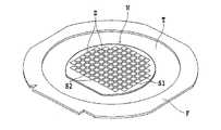
図2に示すように、レーザ加工装置2の加工対象である半導体ウエーハWの表面においては、第1のストリートS1と第2のストリートS2とが直交して形成されており、第1のストリートS1と第2のストリートS2とによって区画された領域に多数のデバイスDが形成されている。 As shown in FIG. 2, on the surface of the semiconductor wafer W to be processed by the
ウエーハWは粘着テープであるダイシングテープTに貼着され、ダイシングテープTの外周部は環状フレームFに貼着されている。これにより、ウエーハWはダイシングテープTを介して環状フレームFに支持された状態となり、図1に示すクランパ30により環状フレームFをクランプすることによりチャックテーブル28上に支持固定される。 The wafer W is attached to a dicing tape T that is an adhesive tape, and the outer periphery of the dicing tape T is attached to an annular frame F. As a result, the wafer W is supported by the annular frame F via the dicing tape T, and is supported and fixed on the chuck table 28 by clamping the annular frame F by the
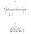
次に図4乃至図8を参照して、本発明実施形態の半導体ウエーハのレーザ加工方法について詳細に説明する。本発明の半導体ウエーハのレーザ加工方法では、図4及び図5(A)に示すように、半導体ウエーハWに対して吸収性を有する波長のパルスレーザビーム37を集光器36で集光して半導体ウエーハWの表面に照射しつつ、チャックテーブル28を図5(A)において一端(図5(A)で左端)から矢印X1で示す方向に所定の加工送り速度で移動させる。 Next, with reference to FIGS. 4 to 8, the laser processing method of the semiconductor wafer according to the embodiment of the present invention will be described in detail. In the laser processing method for a semiconductor wafer according to the present invention, as shown in FIGS. 4 and 5A, a
そして、ストリートS1の他端(図5(A)の右端)が集光器36の照射位置に達したら、パルスレーザビームの照射を停止すると共にチャックテーブル28の移動を停止する。その結果、半導体ウエーハWには、図5(B)に示すようにストリートS1に沿ってレーザ加工溝74が形成される。 When the other end of the street S1 (the right end in FIG. 5A) reaches the irradiation position of the
全ての第1のストリートS1に沿ってレーザ加工溝74を形成したら、チャックテーブル28を90度回転する。次いで、第1のストリートS1と直交する全ての第2のストリートS2に沿って同様なレーザ加工溝74を形成する。その結果、半導体ウエーハWには全てのストリートS1,S2に沿ってレーザ加工溝74が形成される。 When the
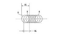
本発明のレーザ加工方法では、集光器36から出力されるパルスレーザビームの繰り返し周波数、パルス幅、スポット径D1及び加工送り速度を最適に設定することにより、図6に示すように、隣接するパルスレーザビームのスポットの加工送り方向の重なり量(オーバーラップ量)OLを以下の範囲内に調整するのが好ましい。スポット径をD1とすると、16D1/20≦OL≦19D1/20
このように全てのストリートS1,S2に沿ってレーザ加工溝74を形成したならば、次に図7に示すような分割装置80を使用して半導体ウエーハWをレーザ加工溝74に沿って個々のチップに分割するウエーハ分割工程を実施する。In the laser processing method of the present invention, the repetition frequency, pulse width, spot diameter D1 and processing feed speed of the pulse laser beam output from the
If the
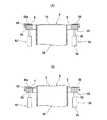
図7に示す分割装置80は、環状フレームFを保持するフレーム保持手段82と、フレーム保持手段82に保持された環状フレームFに装着された粘着テープTを拡張するテープ拡張手段84を具備している。 7 includes a
フレーム保持手段82は、環状のフレーム保持部材86と、フレーム保持部材86の外周に配設された固定手段としての複数のクランプ88から構成される。フレーム保持部86の上面は環状フレームFを載置する載置面86aを形成しており、この載置面86a上に環状フレームFが載置される。 The frame holding means 82 includes an annular
そして、載置面86a上に載置された環状フレームFは、クランプ88によってフレーム保持部材86に固定される。このように構成されたフレーム保持手段82はテープ拡張手段84によって上下方向に移動可能に支持されている。 The annular frame F placed on the
テープ拡張手段84は、環状のフレーム保持部材86の内側に配設された拡張ドラム90を具備している。この拡張ドラム90は、環状フレームFの内径より小さく、該環状フレームFに装着された粘着テープTに貼着される半導体ウエーハWの外径より大きい内径を有している。 The tape expansion means 84 includes an
拡張ドラム90はその下端に一体的に形成された支持フランジ92を有している。テープ拡張手段84は更に、環状のフレーム保持部材86を上下方向に移動する駆動手段94を具備している。この駆動手段94は支持フランジ92上に配設された複数のエアシリンダ96から構成されており、そのピストンロッド98がフレーム保持部材86の下面に連結されている。 The
複数のエアシリンダ96から構成される駆動手段94は、環状のフレーム保持部材86をその載置面86aが拡張ドラム90の上端と略同一高さとなる基準位置と、拡張ドラム90の上端より所定量下方の拡張位置の間を上下方向に移動する。 The driving means 94 composed of a plurality of
以上のように構成された分割装置80を用いて実施する半導体ウエーハ分割工程について図8(A)及び図8(B)を参照して説明する。図8(A)に示すように、半導体ウエーハWを粘着テープTを介して支持した環状フレームFを、フレーム保持部材86の載置面86a上に載置し、クランプ88によってフレーム保持部材86を固定する。このとき、フレーム保持部材86はその載置面86aが拡張ドラム90の上端と略同一高さとなる基準位置に位置付けられる。 A semiconductor wafer dividing step performed using the dividing
次いで、エアシリンダ96を駆動してフレーム保持部材86を図8(B)に示す拡張位置に下降する。これにより、フレーム保持部材86の載置面86a上に固定されている環状フレームFも下降するため、環状フレームFに装着された粘着テープTは拡張ドラム90の上端縁に当接して主に半径方向に拡張される。 Next, the
その結果、粘着テープTに貼着されている半導体ウエーハWには放射状に引張力が作用する。このように半導体ウエーハWに放射状に引張力が作用すると、半導体ウエーハWはレーザ加工溝74に沿って破断され、個々の半導体チップ(デバイス)Dに分割される。 As a result, a tensile force acts radially on the semiconductor wafer W adhered to the adhesive tape T. When a tensile force is applied to the semiconductor wafer W in a radial manner in this way, the semiconductor wafer W is broken along the
本発明の半導体ウエーハのレーザ加工方法では、半導体ウエーハWを分割して得られたデバイスの抗折強度の向上が目的であり、デバイスの抗折強度が800MPa以上となる加工条件を調べるために以下の実験を行った。 In the laser processing method of the semiconductor wafer of the present invention, the purpose is to improve the bending strength of the device obtained by dividing the semiconductor wafer W, and in order to investigate the processing conditions for the device to have a bending strength of 800 MPa or more, The experiment was conducted.
波長1064nm、532nm、355nmの各レーザビームについてパルス幅を30ns、10ns、5ns、3ns、2ns、1ns、100ps、50ps、10psと変化させるとともに、各パルス幅において出力を変化させて所望のレーザ加工が施される1パルス当たりのエネルギーを実験で求め、そのエネルギーをパルス幅で割り算するとともに、スポットの面積で割り算してピークエネルギー密度を算出し、パルス幅とピークエネルギー密度と抗折強度との関係を調べた。 For each laser beam having a wavelength of 1064 nm, 532 nm, and 355 nm, the pulse width is changed to 30 ns, 10 ns, 5 ns, 3 ns, 2 ns, 1 ns, 100 ps, 50 ps, and 10 ps, and the output is changed in each pulse width to perform desired laser processing. The energy per pulse to be applied is determined by experiment, and the energy is divided by the pulse width, and the peak energy density is calculated by dividing the energy by the area of the spot, and the relationship between the pulse width, the peak energy density, and the bending strength. I investigated.
ここで、ピークエネルギー密度(W/cm2)=平均出力(W)/(繰り返し周波数(Hz)×スポット面積(cm2)×パルス幅(s))の関係がある。その結果、波長1064nm、532nm、355nmの各レーザビームについてほとんど同様の以下の結果が得られた。Here, there is a relationship of peak energy density (W / cm2 ) = average output (W) / (repetition frequency (Hz) × spot area (cm2 ) × pulse width (s)). As a result, almost the following results were obtained for the laser beams with wavelengths of 1064 nm, 532 nm, and 355 nm.
(実験1) 繰り返し周波数:10kHz、平均出力:0.1W、パルス幅:2ns、スポット径:φ10μm、送り速度:10mm/s、ピークエネルギー密度:6.35GW/cm2で半導体ウエーハにレーザ加工溝を形成してから個々のデバイスに分割し、デバイスの抗折強度を測定したところ800MPaであった。(Experiment 1) Repetition frequency: 10 kHz, average output: 0.1 W, pulse width: 2 ns, spot diameter: φ10 μm, feed rate: 10 mm / s, peak energy density: 6.35 GW / cm2 , laser processing groove on semiconductor wafer After forming the film, it was divided into individual devices, and the bending strength of the devices was measured and found to be 800 MPa.
(実験2) 繰り返し周波数:100kHz、平均出力:0.1W、パルス幅:10ps、スポット径:φ10μm、送り速度:100mm/s、ピークエネルギー密度:63.66GW/cm2で半導体ウエーハにレーザ加工溝を形成してから個々のデバイスに分割し、デバイスの抗折強度を測定したところ1800MPaであった。(Experiment 2) Repetition frequency: 100 kHz, average output: 0.1 W, pulse width: 10 ps, spot diameter: φ10 μm, feed rate: 100 mm / s, peak energy density: 63.66 GW / cm2 , laser processing groove on semiconductor wafer After forming the film, it was divided into individual devices, and the bending strength of the devices was measured and found to be 1800 MPa.
(実験3) 繰り返し周波数:100kHz、平均出力:0.3W、パルス幅:10ps、スポット径:φ10μm、送り速度:100mm/s、ピークエネルギー密度:190.9GW/cm2で半導体ウエーハにレーザ加工溝を形成してから個々のデバイスに分割し、デバイスの抗折強度を測定したところ1000MPaであった。(Experiment 3) Repetition frequency: 100 kHz, average output: 0.3 W, pulse width: 10 ps, spot diameter: φ10 μm, feed rate: 100 mm / s, peak energy density: 190.9 GW / cm2 , laser processing groove on semiconductor wafer After forming the film, it was divided into individual devices, and the bending strength of the devices was measured and found to be 1000 MPa.
(実験4) 繰り返し周波数:100kHz、平均出力:0.4W、パルス幅:10ps、スポット径:φ10μm、送り速度:100mm/s、ピークエネルギー密度:254.6GW/cm2で半導体ウエーハにレーザ加工溝を形成してから個々のデバイスに分割し、デバイスの抗折強度を測定したところ500MPaであった。(Experiment 4) Repetition frequency: 100 kHz, average output: 0.4 W, pulse width: 10 ps, spot diameter: φ10 μm, feed rate: 100 mm / s, peak energy density: 254.6 GW / cm2 , laser processing groove on semiconductor wafer After forming the film, it was divided into individual devices, and the bending strength of the devices was measured and found to be 500 MPa.
(実験5) 繰り返し周波数:10kHz、平均出力:1.0W、パルス幅:10ns、スポット径:φ10μm、送り速度:10mm/s、ピークエネルギー密度:12.7GW/cm2で半導体ウエーハにレーザ加工溝を形成してから個々のデバイスに分割し、デバイスの抗折強度を測定したところ400MPaであった。(Experiment 5) Repetition frequency: 10 kHz, average output: 1.0 W, pulse width: 10 ns, spot diameter: φ10 μm, feed rate: 10 mm / s, peak energy density: 12.7 GW / cm2 , laser processing groove on semiconductor wafer After forming the film, it was divided into individual devices, and the bending strength of the devices was measured and found to be 400 MPa.
(実験6) 繰り返し周波数:10kHz、平均出力:1.0W、パルス幅:5ns、スポット径:φ10μm、送り速度:10mm/s、ピークエネルギー密度:25.4GW/cm2で半導体ウエーハにレーザ加工溝を形成してから個々のデバイスに分割し、デバイスの抗折強度を測定したところ500MPaであった。(Experiment 6) Repetition frequency: 10 kHz, average output: 1.0 W, pulse width: 5 ns, spot diameter: φ10 μm, feed rate: 10 mm / s, peak energy density: 25.4 GW / cm2 , laser processing groove on semiconductor wafer After forming the film, it was divided into individual devices, and the bending strength of the devices was measured and found to be 500 MPa.
(実験7) 繰り返し周波数:10kHz、平均出力:0.1W、パルス幅:3ns、スポット径:φ10μm、送り速度:10mm/s、ピークエネルギー密度:4.2GW/cm2で半導体ウエーハにレーザ加工溝を形成してから個々のデバイスに分割し、デバイスの抗折強度を測定したところ550MPaであった。(Experiment 7) Repetition frequency: 10 kHz, average output: 0.1 W, pulse width: 3 ns, spot diameter: φ10 μm, feed rate: 10 mm / s, peak energy density: 4.2 GW / cm2 , laser processing groove on semiconductor wafer After forming the film, it was divided into individual devices, and the bending strength of the devices was measured and found to be 550 MPa.
(実験8) 繰り返し周波数:10kHz、平均出力:0.2W、パルス幅:3ns、スポット径:φ10μm、送り速度:10mm/s、ピークエネルギー密度:8.2GW/cm2で半導体ウエーハにレーザ加工溝を形成してから個々のデバイスに分割し、デバイスの抗折強度を測定したところ500MPaであった。(Experiment 8) Repetition frequency: 10 kHz, average output: 0.2 W, pulse width: 3 ns, spot diameter: φ10 μm, feed rate: 10 mm / s, peak energy density: 8.2 GW / cm2 , laser processing groove on semiconductor wafer After forming the film, it was divided into individual devices, and the bending strength of the devices was measured and found to be 500 MPa.
(実験9) 繰り返し周波数:10kHz、平均出力:0.07W、パルス幅:2ns、スポット径:φ10μm、送り速度:10mm/s、ピークエネルギー密度:4.5GW/cm2で半導体ウエーハにレーザ加工溝を形成してから個々のデバイスに分割し、デバイスの抗折強度を測定したところ550MPaであった。(Experiment 9) Repetition frequency: 10 kHz, average output: 0.07 W, pulse width: 2 ns, spot diameter: φ10 μm, feed rate: 10 mm / s, peak energy density: 4.5 GW / cm2 , laser processing groove on semiconductor wafer After forming the film, it was divided into individual devices, and the bending strength of the devices was measured and found to be 550 MPa.
以上の実験結果から、抗折強度が800MPa以上のデバイスを得るためには、照射されるパルスレーザビームのパルス幅が2ns以下であり、且つピークエネルギー密度が5GW/cm2〜200GW/cm2の範囲内であることが必要であると結論される。From the above experimental results, in order to obtain a device having a bending strength of 800 MPa or more, the pulse width of the irradiated pulse laser beam is 2 ns or less, and the peak energy density is 5 GW / cm2 to 200 GW / cm2 . It is concluded that it is necessary to be within range.
また、図6を参照して説明したように、隣接するスポットSの加工送り方向におけるオーバーラップ率が16/20〜19/20の範囲内にあることが好ましい。更に、半導体ウエーハW上でのレーザビームのスポット径はφ5μm〜φ15μmの範囲内にあることが好ましい。 In addition, as described with reference to FIG. 6, it is preferable that the overlap rate of the adjacent spots S in the processing feed direction is in the range of 16/20 to 19/20. Further, the spot diameter of the laser beam on the semiconductor wafer W is preferably in the range of φ5 μm to φ15 μm.
W 半導体ウエーハ
T 粘着テープ(ダイシングテープ)
F 環状フレーム
D デバイス
2 レーザ加工装置
28 チャックテーブル
34 レーザビーム照射ユニット
36 集光器
74 レーザ加工溝
80 分割装置
82 フレーム保持手段
84 テープ拡張手段
86 フレーム保持部材
90 拡張ドラム
96 エアシリンダW Semiconductor wafer T Adhesive tape (dicing tape)
F annular
Claims (2)
Translated fromJapanese半導体ウエーハの分割予定ラインに沿って半導体ウエーハに対して吸収性を有する波長のパルスレーザビームを照射して半導体ウエーハにレーザ加工溝を形成する加工溝形成工程を具備し、
該加工溝形成工程で照射されるパルスレーザビームのパルス幅が2ns以下であり、ピークエネルギー密度が5GW/cm2〜200GW/cm2であり、
該加工溝形成工程では、半導体ウエーハに集光されるスポットがスポット径の16/20〜19/20の範囲内の重なり量でもって半導体ウエーハを加工送りして該加工溝を形成することを特徴とする半導体ウエーハのレーザ加工方法。A method for processing a semiconductor wafer,
A processing groove forming step of forming a laser processing groove on a semiconductor wafer by irradiating a semiconductor wafer with a pulsed laser beam having a wavelength having an absorptivity along the division line of the semiconductor wafer;
The machining pulse width of the pulse laser beam emitted by the groove forming step is not more 2ns or less,Ri peak energy density 5GW / cm2 ~200GW / cm2der,
In the processing groove forming step, the processing groove is formed by processing and feeding the semiconductor wafer with an overlapping amount of spots focused on the semiconductor wafer within a range of 16/20 to 19/20 of the spot diameter. A semiconductor wafer laser processing method.
Priority Applications (5)
| Application Number | Priority Date | Filing Date | Title |
|---|---|---|---|
| JP2009123434AJP5340806B2 (en) | 2009-05-21 | 2009-05-21 | Laser processing method of semiconductor wafer |
| TW99107586ATWI473153B (en) | 2009-05-21 | 2010-03-16 | Semiconductor wafer laser processing method (a) |
| KR1020100032260AKR101597369B1 (en) | 2009-05-21 | 2010-04-08 | Laser processing method of semiconductor wafer |
| US12/771,749US8252667B2 (en) | 2009-05-21 | 2010-04-30 | Laser processing method for semiconductor wafer |
| CN201010185018.5ACN101890578B (en) | 2009-05-21 | 2010-05-21 | Laser processing method for semiconductor wafer |
Applications Claiming Priority (1)
| Application Number | Priority Date | Filing Date | Title |
|---|---|---|---|
| JP2009123434AJP5340806B2 (en) | 2009-05-21 | 2009-05-21 | Laser processing method of semiconductor wafer |
Publications (2)
| Publication Number | Publication Date |
|---|---|
| JP2010272697A JP2010272697A (en) | 2010-12-02 |
| JP5340806B2true JP5340806B2 (en) | 2013-11-13 |
Family
ID=43100007
Family Applications (1)
| Application Number | Title | Priority Date | Filing Date |
|---|---|---|---|
| JP2009123434AActiveJP5340806B2 (en) | 2009-05-21 | 2009-05-21 | Laser processing method of semiconductor wafer |
Country Status (5)
| Country | Link |
|---|---|
| US (1) | US8252667B2 (en) |
| JP (1) | JP5340806B2 (en) |
| KR (1) | KR101597369B1 (en) |
| CN (1) | CN101890578B (en) |
| TW (1) | TWI473153B (en) |
Families Citing this family (20)
| Publication number | Priority date | Publication date | Assignee | Title |
|---|---|---|---|---|
| JP5193326B2 (en)* | 2011-02-25 | 2013-05-08 | 三星ダイヤモンド工業株式会社 | Substrate processing apparatus and substrate processing method |
| US8648277B2 (en)* | 2011-03-31 | 2014-02-11 | Electro Scientific Industries, Inc. | Laser direct ablation with picosecond laser pulses at high pulse repetition frequencies |
| JP5912283B2 (en)* | 2011-04-20 | 2016-04-27 | 株式会社ディスコ | Processing method of adhesive tape and wafer |
| JP6000700B2 (en)* | 2012-07-10 | 2016-10-05 | 株式会社ディスコ | Laser processing method |
| JP2014104484A (en)* | 2012-11-27 | 2014-06-09 | Disco Abrasive Syst Ltd | Laser processing apparatus |
| EP2754524B1 (en)* | 2013-01-15 | 2015-11-25 | Corning Laser Technologies GmbH | Method of and apparatus for laser based processing of flat substrates being wafer or glass element using a laser beam line |
| JP6208430B2 (en)* | 2013-01-25 | 2017-10-04 | 株式会社ディスコ | Laser processing method |
| JP6334235B2 (en) | 2014-04-07 | 2018-05-30 | 株式会社ディスコ | Laser processing equipment |
| JP6285784B2 (en) | 2014-04-09 | 2018-02-28 | 株式会社ディスコ | Height position detector |
| KR20150130835A (en)* | 2014-05-14 | 2015-11-24 | 주식회사 이오테크닉스 | Laser processing method for cutting semiconductor with metal layer and laser processing apparatus |
| CN106031961B (en)* | 2015-03-20 | 2019-02-05 | 元壤实业(上海)有限公司 | A method of processing conducting foam wire casing |
| DE102016215473B4 (en)* | 2015-09-10 | 2023-10-26 | Disco Corporation | Method for processing a substrate |
| CN105215545A (en)* | 2015-11-11 | 2016-01-06 | 苏州天弘激光股份有限公司 | Wafer straight cutting machine |
| JP6666173B2 (en)* | 2016-03-09 | 2020-03-13 | 株式会社ディスコ | Laser processing equipment |
| CN107302042B (en)* | 2017-05-17 | 2019-11-29 | 华灿光电(浙江)有限公司 | Preparation method of light emitting diode chip and light conversion device |
| JP6980421B2 (en)* | 2017-06-16 | 2021-12-15 | 株式会社ディスコ | Wafer processing method |
| JP7066263B2 (en)* | 2018-01-23 | 2022-05-13 | 株式会社ディスコ | Machining method, etching equipment, and laser processing equipment |
| CN110480161A (en)* | 2019-07-04 | 2019-11-22 | 大族激光科技产业集团股份有限公司 | The cutting method and device of chip |
| CN111331262B (en)* | 2020-03-23 | 2021-12-24 | 广州兴森快捷电路科技有限公司 | Packaging carrier plate and method for processing inner groove of metal cavity |
| CN116921872A (en)* | 2023-06-27 | 2023-10-24 | 广东原点智能技术有限公司 | Laser plane grinding method |
Family Cites Families (13)
| Publication number | Priority date | Publication date | Assignee | Title |
|---|---|---|---|---|
| WO2000060668A1 (en)* | 1999-04-07 | 2000-10-12 | Siemens Solar Gmbh | Device and method for removing thin layers on a support material |
| JP3722731B2 (en)* | 2000-09-13 | 2005-11-30 | 浜松ホトニクス株式会社 | Laser processing method |
| JP3408805B2 (en)* | 2000-09-13 | 2003-05-19 | 浜松ホトニクス株式会社 | Cutting origin region forming method and workpiece cutting method |
| US6770544B2 (en)* | 2001-02-21 | 2004-08-03 | Nec Machinery Corporation | Substrate cutting method |
| EP2400539B1 (en)* | 2002-03-12 | 2017-07-26 | Hamamatsu Photonics K.K. | Substrate dividing method |
| US7015418B2 (en)* | 2002-05-17 | 2006-03-21 | Gsi Group Corporation | Method and system for calibrating a laser processing system and laser marking system utilizing same |
| US20050087522A1 (en)* | 2003-10-24 | 2005-04-28 | Yunlong Sun | Laser processing of a locally heated target material |
| JP2005228892A (en)* | 2004-02-12 | 2005-08-25 | Toshiba Corp | Semiconductor wafer, semiconductor element and manufacturing method thereof |
| US20060189091A1 (en)* | 2004-11-11 | 2006-08-24 | Bo Gu | Method and system for laser hard marking |
| JP4942313B2 (en) | 2005-07-07 | 2012-05-30 | 株式会社ディスコ | Wafer laser processing method |
| JP2007021528A (en)* | 2005-07-15 | 2007-02-01 | Matsushita Electric Ind Co Ltd | Laser processing apparatus and adjustment method thereof |
| JP2008071870A (en)* | 2006-09-13 | 2008-03-27 | Toshiba Corp | Manufacturing method of semiconductor device |
| JP2008227276A (en)* | 2007-03-14 | 2008-09-25 | Disco Abrasive Syst Ltd | Wafer division method |
- 2009
- 2009-05-21JPJP2009123434Apatent/JP5340806B2/enactiveActive
- 2010
- 2010-03-16TWTW99107586Apatent/TWI473153B/enactive
- 2010-04-08KRKR1020100032260Apatent/KR101597369B1/enactiveActive
- 2010-04-30USUS12/771,749patent/US8252667B2/enactiveActive
- 2010-05-21CNCN201010185018.5Apatent/CN101890578B/enactiveActive
Also Published As
| Publication number | Publication date |
|---|---|
| KR101597369B1 (en) | 2016-02-24 |
| TW201042714A (en) | 2010-12-01 |
| CN101890578B (en) | 2015-02-04 |
| JP2010272697A (en) | 2010-12-02 |
| TWI473153B (en) | 2015-02-11 |
| US20100297830A1 (en) | 2010-11-25 |
| US8252667B2 (en) | 2012-08-28 |
| CN101890578A (en) | 2010-11-24 |
| KR20100126185A (en) | 2010-12-01 |
Similar Documents
| Publication | Publication Date | Title |
|---|---|---|
| JP5340806B2 (en) | Laser processing method of semiconductor wafer | |
| JP5473414B2 (en) | Laser processing equipment | |
| JP5340808B2 (en) | Laser processing method of semiconductor wafer | |
| JP5473415B2 (en) | Laser processing equipment | |
| JP5528015B2 (en) | Laser processing equipment | |
| JP6308919B2 (en) | Wafer processing method | |
| JP2011108708A (en) | Method of processing wafer | |
| JP2016054205A (en) | Wafer processing method | |
| JP2016076520A (en) | Wafer processing method | |
| JP2017059684A (en) | Wafer processing method | |
| JP5340807B2 (en) | Processing method of semiconductor wafer | |
| JP5441629B2 (en) | Wafer processing method | |
| JP2016042516A (en) | Wafer processing method | |
| JP6308913B2 (en) | Wafer processing method | |
| JP6293017B2 (en) | Wafer processing method | |
| JP2016058429A (en) | Wafer processing method | |
| JP2017059688A (en) | Wafer | |
| JP2017092128A (en) | Processing method of wafer | |
| JP2016058430A (en) | Wafer processing method | |
| JP2016058431A (en) | Wafer processing method | |
| JP2016072278A (en) | Wafer processing method | |
| JP2017092126A (en) | Processing method of wafer | |
| JP2016072274A (en) | Wafer processing method | |
| JP2016054208A (en) | Wafer processing method | |
| JP2016042515A (en) | Wafer processing method |
Legal Events
| Date | Code | Title | Description |
|---|---|---|---|
| A621 | Written request for application examination | Free format text:JAPANESE INTERMEDIATE CODE: A621 Effective date:20120413 | |
| A131 | Notification of reasons for refusal | Free format text:JAPANESE INTERMEDIATE CODE: A131 Effective date:20130507 | |
| A521 | Request for written amendment filed | Free format text:JAPANESE INTERMEDIATE CODE: A523 Effective date:20130627 | |
| TRDD | Decision of grant or rejection written | ||
| A01 | Written decision to grant a patent or to grant a registration (utility model) | Free format text:JAPANESE INTERMEDIATE CODE: A01 Effective date:20130806 | |
| A61 | First payment of annual fees (during grant procedure) | Free format text:JAPANESE INTERMEDIATE CODE: A61 Effective date:20130807 | |
| R150 | Certificate of patent or registration of utility model | Ref document number:5340806 Country of ref document:JP Free format text:JAPANESE INTERMEDIATE CODE: R150 Free format text:JAPANESE INTERMEDIATE CODE: R150 | |
| R250 | Receipt of annual fees | Free format text:JAPANESE INTERMEDIATE CODE: R250 | |
| R250 | Receipt of annual fees | Free format text:JAPANESE INTERMEDIATE CODE: R250 | |
| R250 | Receipt of annual fees | Free format text:JAPANESE INTERMEDIATE CODE: R250 | |
| R250 | Receipt of annual fees | Free format text:JAPANESE INTERMEDIATE CODE: R250 | |
| R250 | Receipt of annual fees | Free format text:JAPANESE INTERMEDIATE CODE: R250 | |
| R250 | Receipt of annual fees | Free format text:JAPANESE INTERMEDIATE CODE: R250 | |
| R250 | Receipt of annual fees | Free format text:JAPANESE INTERMEDIATE CODE: R250 | |
| R250 | Receipt of annual fees | Free format text:JAPANESE INTERMEDIATE CODE: R250 | |
| R250 | Receipt of annual fees | Free format text:JAPANESE INTERMEDIATE CODE: R250 | |
| R250 | Receipt of annual fees | Free format text:JAPANESE INTERMEDIATE CODE: R250 |