JP5337751B2 - Polarizing plate and liquid crystal display device - Google Patents
Polarizing plate and liquid crystal display deviceDownload PDFInfo
- Publication number
- JP5337751B2 JP5337751B2JP2010056940AJP2010056940AJP5337751B2JP 5337751 B2JP5337751 B2JP 5337751B2JP 2010056940 AJP2010056940 AJP 2010056940AJP 2010056940 AJP2010056940 AJP 2010056940AJP 5337751 B2JP5337751 B2JP 5337751B2
- Authority
- JP
- Japan
- Prior art keywords
- polarizing layer
- dye
- liquid crystal
- polarizing
- base film
- Prior art date
- Legal status (The legal status is an assumption and is not a legal conclusion. Google has not performed a legal analysis and makes no representation as to the accuracy of the status listed.)
- Expired - Fee Related
Links
Images


Landscapes
- Liquid Crystal (AREA)
- Polarising Elements (AREA)
Abstract
Description
Translated fromJapanese本発明は、偏光板および液晶表示装置に関し、特に、液晶表示パネルに設ける偏光部材に適用して有効な技術に関するものである。 The present invention relates to a polarizing plate and a liquid crystal display device, and particularly to a technique effective when applied to a polarizing member provided in a liquid crystal display panel.
表示装置は、情報を視覚的に人間に伝えるデバイスであり、高度な情報社会となった現代では、人間、社会にとって重要な存在となっている。特に、液晶表示装置(LCD: Liquid Crystal Display)は、近年、性能が著しく向上しており、たとえば、携帯電話端末に搭載される表示装置、パーソナルコンピューターに接続して用いる表示装置、大画面テレビ等に採用されている。 A display device is a device that visually conveys information to a human being, and has become an important presence for human beings and society in the present age when it has become an advanced information society. In particular, the performance of liquid crystal display (LCD) has been remarkably improved in recent years. For example, a display device mounted on a mobile phone terminal, a display device connected to a personal computer, a large screen television, etc. Has been adopted.
液晶表示装置の多くは、一対の基板の間に液晶層を設けた液晶表示パネルと、バックライト(照明装置)とを有し、バックライトからの面状光線を液晶表示パネルで変調することにより、映像や画像などの情報を視覚的に人間に伝える。このとき、液晶表示パネルは、液晶層を挟んで配置される一対の偏光層を有する。従来の液晶表示パネルでは、偏光層としてフィルム状の偏光板(以下、フィルム偏光板と呼ぶ。)を用いることが多い。偏光層としてフィルム偏光板を用いる場合、当該フィルム偏光板は、それぞれの基板における液晶層と対向する面の裏面に接着材(粘着材を含む。)で貼り付けている。 Many liquid crystal display devices have a liquid crystal display panel in which a liquid crystal layer is provided between a pair of substrates, and a backlight (illumination device). By modulating a planar light beam from the backlight with the liquid crystal display panel, Visually convey information such as images and images to humans. At this time, the liquid crystal display panel has a pair of polarizing layers arranged with the liquid crystal layer interposed therebetween. In a conventional liquid crystal display panel, a film-like polarizing plate (hereinafter referred to as a film polarizing plate) is often used as a polarizing layer. When using a film polarizing plate as a polarizing layer, the said film polarizing plate is affixed on the back surface of the surface which opposes the liquid-crystal layer in each board | substrate with the adhesive material (an adhesive material is included).
液晶表示パネルにおける偏光層は、バックライトからの光の透過光量の制御に用いられるものであり、吸収軸および透過軸の方向が重要になる。液晶表示パネルにおける偏光層の吸収軸の方向は、当該液晶表示パネルにおける画素の構成によって決まり、たとえば、基板平面の端辺と平行にする場合もあるし、所定の角度だけ傾けることもある。 The polarizing layer in the liquid crystal display panel is used for controlling the amount of light transmitted from the backlight, and the directions of the absorption axis and the transmission axis are important. The direction of the absorption axis of the polarizing layer in the liquid crystal display panel is determined by the configuration of the pixels in the liquid crystal display panel, and may be, for example, parallel to the edge of the substrate plane or tilted by a predetermined angle.
フィルム偏光板は、たとえば、ポリビニルアルコール系の樹脂フィルムを一軸延伸し、その表面にヨウ素や二色性染料等を吸着配向させた偏光層を有するものであり、透過軸は延伸方向に限定される。そのため、液晶表示パネルにおける偏光層の吸収軸の方向を基板平面の端辺に対して所定の角度だけ傾ける場合、傾ける角度に合わせてフィルム偏光板を切断する必要があり、無駄になる部分が生じる。 The film polarizing plate has, for example, a polarizing layer obtained by uniaxially stretching a polyvinyl alcohol-based resin film and adsorbing and orienting iodine or a dichroic dye on the surface thereof, and the transmission axis is limited to the stretching direction. . Therefore, when the direction of the absorption axis of the polarizing layer in the liquid crystal display panel is tilted by a predetermined angle with respect to the edge of the substrate plane, it is necessary to cut the film polarizing plate in accordance with the tilt angle, resulting in useless portions. .
また、フィルム偏光板は、たとえば、上記のような偏光層を一対の保護フィルムで挟んだ構成になっている。またさらに、フィルム偏光板は、上記のように、接着材を用いて基板に貼り付ける必要がある。そのため、フィルム偏光板を貼り付ける液晶表示パネルの製造方法は、工程数が多くなり、たとえば、製造コストの低減に不利である。 Moreover, the film polarizing plate has a configuration in which the polarizing layer as described above is sandwiched between a pair of protective films, for example. Furthermore, as described above, the film polarizing plate needs to be attached to the substrate using an adhesive. Therefore, the method for manufacturing a liquid crystal display panel to which the film polarizing plate is attached has a large number of steps, which is disadvantageous in reducing manufacturing costs, for example.
以上のようなことから、近年の液晶表示パネルの製造方法では、たとえば、液晶層を挟む基板の表面に偏光層を直接形成する方法が提案されている(たとえば、特許文献1を参照。)。 From the above, in recent liquid crystal display panel manufacturing methods, for example, a method of directly forming a polarizing layer on the surface of a substrate sandwiching the liquid crystal layer has been proposed (see, for example, Patent Document 1).
基板の表面に偏光層を直接形成する場合、通常、当該基板の表面に設けるのは当該偏光層と、必要に応じて設ける保護層だけである。そのため、基板の表面に偏光層を直接形成する液晶表示パネルの製造方法は、フィルム偏光板を用いる液晶表示パネルの製造方法に比べて製造効率がよい。また、基板の表面に偏光層を直接形成する液晶表示パネルは、フィルム偏光板を用いる液晶表示パネルに比べて薄型化が可能である。 When the polarizing layer is directly formed on the surface of the substrate, usually, only the polarizing layer and a protective layer provided as necessary are provided on the surface of the substrate. Therefore, the manufacturing method of the liquid crystal display panel in which the polarizing layer is directly formed on the surface of the substrate is more efficient than the manufacturing method of the liquid crystal display panel using the film polarizing plate. Further, a liquid crystal display panel in which a polarizing layer is directly formed on the surface of a substrate can be made thinner than a liquid crystal display panel using a film polarizing plate.
基板の表面に偏光層を直接形成する場合、当該偏光層は、所定の材料(以下、偏光層材料と呼ぶ。)を一方向に圧力を加えながら引き伸ばすことで形成される。このとき、偏光層の色素は、偏光層材料を塗布したときに生じる当該材料の流動の方向、下地の濡れ性による流動の方向によって配向する。したがって、色素の配向性には、偏光層材料の流動の方向が重要である。 When the polarizing layer is directly formed on the surface of the substrate, the polarizing layer is formed by stretching a predetermined material (hereinafter referred to as a polarizing layer material) while applying pressure in one direction. At this time, the dye of the polarizing layer is oriented depending on the direction of flow of the material generated when the polarizing layer material is applied and the direction of flow due to the wettability of the base. Therefore, the direction of flow of the polarizing layer material is important for the orientation of the dye.
偏光層は、色素が一方向に並ぶことによって光学特性が向上する。液晶表示パネルの基板に偏光層を直接形成する場合、当該偏光層は、たとえば、ガラス基板の上に形成される。しかしながら、偏光層を直接ガラス基板に形成すると色素の配向性が低くなってしまう。これは、以下の理由が考えられる。 Optical properties of the polarizing layer are improved by arranging the dyes in one direction. When the polarizing layer is directly formed on the substrate of the liquid crystal display panel, the polarizing layer is formed on a glass substrate, for example. However, when the polarizing layer is formed directly on the glass substrate, the orientation of the dye is lowered. The following reasons can be considered for this.
偏光層材料では溶媒として、通常、好適である水を用いる。溶媒として水を用いた偏光層材料の場合、親水性の水酸基が存在するガラス基板の表面に塗布すると、当該偏光層材料は引き延ばす方向以外の方向にも濡れ広がる。そのため、偏光層には、引き延ばす方向とは異なる方向に配向する色素が多くなる。このように、ガラス基板に偏光層を直接形成すると、色素を一方向に配向させることが困難であり、偏光層の二色比が低下してしまうという問題がある。なお、二色比というのは、色素の配向性を表すパラメータであり、偏光層における吸収軸の吸光係数k1の対数log(k1)と透過軸の吸光係数k2の対数log(k2)との比log(k1)/log(k2)で表される。 In the polarizing layer material, water which is usually suitable is used as a solvent. In the case of a polarizing layer material using water as a solvent, when applied to the surface of a glass substrate having a hydrophilic hydroxyl group, the polarizing layer material wets and spreads in directions other than the extending direction. For this reason, the polarizing layer contains more dyes that are oriented in a direction different from the extending direction. Thus, when the polarizing layer is directly formed on the glass substrate, it is difficult to orient the dye in one direction, and there is a problem that the dichroic ratio of the polarizing layer is lowered. The dichroic ratio is a parameter representing the orientation of the dye, and is the ratio between the logarithm log (k1) of the absorption coefficient k1 of the absorption axis and the logarithm log (k2) of the absorption coefficient k2 of the transmission axis in the polarizing layer. It is represented by log (k1) / log (k2).
すなわち、偏光層の二色比が低下するということは、透過軸の吸光係数と吸収軸の吸光係数との差が小さくなるということである。したがって、偏光層をガラス基板に直接形成した液晶表示パネルを有する液晶表示装置では、透過率およびコントラスト比が低下してしまう。 That is, the decrease in the dichroic ratio of the polarizing layer means that the difference between the extinction coefficient of the transmission axis and the extinction coefficient of the absorption axis is reduced. Therefore, in a liquid crystal display device having a liquid crystal display panel in which a polarizing layer is directly formed on a glass substrate, the transmittance and contrast ratio are reduced.
このような問題に対しては、たとえば、偏光層と基板との間に色素の配向性を向上させるための下地膜を設けることが考えられる。下地膜は、たとえば、液晶表示パネルにおいて液晶層の電界無印加時の配向を制御するための配向膜を用いることが効果的である。しかしながら、下地膜として配向膜を設けると、当該配向膜による光吸収の影響が発生する。すなわち、偏光層を下地膜(配向膜)の上に形成すると、偏光層における色素の配向性は高くなるものの、透過率が低下してしまう。そのため、基板と偏光層との間に下地膜を設ける方法には、実効的な二色比が低下してしまうという問題がある。 For such a problem, for example, it is conceivable to provide a base film for improving the orientation of the dye between the polarizing layer and the substrate. For example, it is effective to use an alignment film for controlling the alignment of the liquid crystal layer when no electric field is applied in the liquid crystal display panel. However, when an alignment film is provided as a base film, the influence of light absorption by the alignment film occurs. That is, when the polarizing layer is formed on the base film (alignment film), although the orientation of the dye in the polarizing layer increases, the transmittance decreases. Therefore, the method of providing a base film between the substrate and the polarizing layer has a problem that the effective dichroic ratio is lowered.
また、基板と偏光層との間に下地膜を設ける方法には、たとえば、特許文献1のように、下地膜の表面(偏光層を形成する面)に凹凸を設ける方法がある。しかしながら、凹凸を有する下地膜(以下、凹凸下地膜と呼ぶ。)の上に偏光層を形成すると、充分な光学特性が得られないことが、本願発明者らの調査により判明した。 In addition, as a method of providing a base film between the substrate and the polarizing layer, for example, there is a method of providing unevenness on the surface of the base film (surface on which the polarizing layer is formed) as in
凹凸下地膜の上に偏光層材料を塗布した場合、当該偏光層材料の色素は、凹凸の長手方向が透過軸になるように流動し、配向する。しかしながら、凹凸下地膜が親水性膜であると、偏光層材料は凹凸の壁面に沿って流動し、凹凸の長手方向以外の方向に色素が配向してしまう。そのため、凹凸下地膜の上に偏光層を形成した場合、二色比が低下してしまう。 When the polarizing layer material is applied on the uneven base film, the dye of the polarizing layer material flows and is oriented so that the longitudinal direction of the unevenness becomes the transmission axis. However, when the uneven base film is a hydrophilic film, the polarizing layer material flows along the uneven wall surface, and the dye is oriented in a direction other than the longitudinal direction of the unevenness. Therefore, when the polarizing layer is formed on the uneven base film, the dichroic ratio is lowered.
また、特許文献1などに開示されている凹凸下地膜は、凹凸のピッチが可視光波長と近いので、凹凸下地膜の上に形成した偏光層に光が入射すると回折してしまう。そのため、偏光層を通過した光が正面以外の方向に広がり、たとえば、正面方向における透過率およびコントラスト比が低下してしまう。 Moreover, since the uneven | corrugated base film currently disclosed by
このように、従来の方法で基板の表面に偏光層を直接形成した液晶表示パネルを有する液晶表示装置では、偏光層の二色比の低下により、透過率およびコントラスト比が低下するという問題があった。 As described above, the liquid crystal display device having the liquid crystal display panel in which the polarizing layer is directly formed on the surface of the substrate by the conventional method has a problem that the transmittance and the contrast ratio are lowered due to the decrease in the dichroic ratio of the polarizing layer. It was.
またさらに、凹凸下地膜に光が入射すると、反射した光が凹凸によって干渉し、色つきの問題が生じる。そのため、基板と偏光層との間に凹凸下地膜が介在している液晶表示パネルを有する液晶表示装置では、たとえば、外光下における視認性が著しく低下してしまうという問題があった。 Furthermore, when light is incident on the uneven base film, the reflected light interferes with the unevenness, causing a problem of coloring. Therefore, in a liquid crystal display device having a liquid crystal display panel in which an uneven base film is interposed between the substrate and the polarizing layer, for example, there has been a problem that visibility under external light is significantly reduced.
本発明の目的は、たとえば、基板に偏光層が直接形成された液晶表示パネルを有する液晶表示装置の透過率およびコントラスト比を向上させることが可能な技術を提供することにある。 An object of the present invention is to provide a technique capable of improving the transmittance and contrast ratio of a liquid crystal display device having a liquid crystal display panel in which a polarizing layer is directly formed on a substrate, for example.
本発明の前記ならびにその他の目的と新規な特徴は、本明細書の記述および添付図面によって明らかになるであろう。 The above and other objects and novel features of the present invention will be apparent from the description of this specification and the accompanying drawings.
本願において開示される発明のうち、代表的なものの概略を説明すれば、以下の通りである。 The outline of typical inventions among the inventions disclosed in the present application will be described as follows.
(1)基材の上に偏光層が形成された偏光板であって、前記偏光層における前記基材と対向する面には、第1の材料と接している第1の領域と、第2の材料と接している第2の領域と、があり、かつ、前記第1の領域と前記第2の領域とがストライプ状に存在している偏光板である。 (1) A polarizing plate in which a polarizing layer is formed on a base material, wherein a surface of the polarizing layer facing the base material has a first region in contact with the first material, and a second material There is a second region in contact with the material, and the first region and the second region are in a stripe shape.
(2)一対の基板の間に液晶層が挟持された液晶表示パネルを有する液晶表示装置であって、前記一対の基板のうちの一方の基板は、絶縁性の基材と、前記基材における第1の面の上に形成された薄膜積層体と、前記基材における前記第1の面とは反対側の第2の面の上に形成された偏光層とを有し、前記偏光層における前記基材の前記第2の面と対向する面には、第1の材料と接している第1の領域と、第2の材料と接している第2の領域と、があり、かつ、前記第1の領域と前記第2の領域とがストライプ状に存在している液晶表示装置である。 (2) A liquid crystal display device having a liquid crystal display panel in which a liquid crystal layer is sandwiched between a pair of substrates, wherein one of the pair of substrates includes an insulating base material and a base material A thin film stack formed on the first surface, and a polarizing layer formed on the second surface of the substrate opposite to the first surface, the polarizing layer There is a first region in contact with the first material and a second region in contact with the second material on the surface of the base material facing the second surface, and In the liquid crystal display device, the first region and the second region exist in stripes.
本発明によれば、基材(基板)の上に偏光層を直接形成した偏光板における二色比を向上させることができる。そのため、基板に偏光層が直接形成された液晶表示パネルを有する液晶表示装置の透過率およびコントラスト比を向上させることができる。 ADVANTAGE OF THE INVENTION According to this invention, the dichroic ratio in the polarizing plate which formed the polarizing layer directly on the base material (board | substrate) can be improved. Therefore, the transmittance and contrast ratio of a liquid crystal display device having a liquid crystal display panel in which a polarizing layer is directly formed on a substrate can be improved.
以下、本発明について、図面を参照して実施の形態(実施例)とともに詳細に説明する。
なお、実施例を説明するための全図において、同一機能を有するものは、同一符号を付け、その繰り返しの説明は省略する。Hereinafter, the present invention will be described in detail together with embodiments (examples) with reference to the drawings.
In all the drawings for explaining the embodiments, parts having the same function are given the same reference numerals and their repeated explanation is omitted.
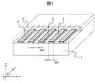
図1は、本発明による実施例1の偏光板の概略構成を示す模式斜視図である。 FIG. 1 is a schematic perspective view showing a schematic configuration of a polarizing plate of Example 1 according to the present invention.
実施例1の偏光板は、たとえば、図1に示すように、基材1、下地膜2、および偏光層3により構成される。このとき、偏光層3は、溶液状の偏光層材料を基材1の表面に塗布して形成されるものであり、フィルム偏光板のようなあらかじめ作製されたものを接着剤(粘着材を含む。)で基材1に貼り付けたものではない。このように基材1の表面に偏光層材料を塗布して形成された偏光層3のことを、本明細書では、基材1(または基板)に直接形成された偏光層と呼んでいる。 For example, as shown in FIG. 1, the polarizing plate of Example 1 includes a
また、基材1における偏光層3を形成する面(以下、基材1の表面と呼ぶ。)には、下地膜2がストライプ状に設けられている。すなわち、偏光層3における基材1と向かい合う面には、基材1に接している第1の領域と、下地膜2に接している第2の領域と、があり、かつ、第1の領域および第2の領域がストライプ状に延在している。 In addition, the
基材1は、透明な基板であり、たとえば、可視波長域の光の吸収が小さいガラス基板が好適である。 The
下地膜2は、偏光層3の色素の配向性を向上させるためのものであり、基材1の表面にストライプ状に設けられている。この下地膜2の幅W1と間隙W2の望ましい値については後述することにし、まず、下地膜2の形成方法について簡単に説明する。 The
下地膜2の材料としては、たとえば、ポリイミドの前駆体モノマーであるポリアミック酸モノマー、光硬化性樹脂モノマー、ポリエステル等が好適である。下地膜2を形成するときには、まず、所定の材料を溶液状にして基材1に塗布した後、乾燥等の後処理を行なってストライプ状ではない均一な下地膜を形成する。 As the material of the
次に、基材1の表面に形成された均一な下地膜に、フォトマスクを通してオゾン雰囲気中で紫外線を照射する。フォトマスクは、石英ガラスに紫外線が透過しにくい金属などの膜を形成し、その膜をフォトリソグラフィなどの技術によってパターニングしたものを用いる。このとき、フォトマスクには、前記金属で形成されたラインがストライプ状に並んだパターンを設ける。 Next, the uniform base film formed on the surface of the
また、紫外線の光源には低圧水銀ランプを用いるとよい。低圧水銀ランプから出た光は波長約185nmおよび約254nmの強度が大きい。この強度の大きい波長の光のエネルギーは、有機材料に含まれる成分(有機物)の化学結合エネルギーより大きいので、当該紫外線を照射することにより有機物の結合を切断できる。そのため、下地膜の上にフォトマスクを設置して紫外線を照射すると、下地膜のうちの、フォトマスクにおけるラインの間隙部分(スペース部分)と重なる領域は分解されて基材1が露出する。また、下地膜のうちのライン部分と重なる領域は紫外線がほとんど当たらないため下地膜2として残る。そのため、基材1の表面には、フォトマスクにおけるパターンを反映したストライプ状の下地膜2が形成される。 A low-pressure mercury lamp may be used as the ultraviolet light source. The light emitted from the low-pressure mercury lamp has a large intensity at wavelengths of about 185 nm and about 254 nm. Since the energy of light having a wavelength with a high intensity is larger than the chemical bond energy of the component (organic substance) contained in the organic material, the bond of the organic substance can be broken by irradiating the ultraviolet light. For this reason, when a photomask is placed on the base film and irradiated with ultraviolet rays, the
なお、下地膜2の膜厚は0.02μm以下とする。これは、たとえば、基材1の表面と下地膜2とで構成される凹凸の高低差が可視波長に近いと下地膜2に入射した光が回折してしまい、偏光板の透過率およびコントラスト比を低下させる原因になるからである。また、下地膜2の膜厚を0.02μm以下にするのには、たとえば、偏光板に入射した光が基材1の表面と下地膜2とで構成される凹凸部分で反射することにより干渉して色つきの問題が生じることを防ぐ目的もある。 The film thickness of the
ところで、上記のように下地膜の上にフォトマスクを設置して紫外線を照射することでストライプ状の下地膜2を形成する場合、下地膜2の幅W1および間隙W2は、それぞれ、フォトマスクにおけるラインの幅および間隙と概ね一致する。フォトマスクにおけるラインの幅および間隙は、フォトマスクの作製方法を考慮すると、それぞれ0.05μmから50μmの範囲にすることが望ましい。また、基材1としてガラス基板を用い、下地膜2を有しない基材1の表面に偏光層3を直接形成した場合、偏光層3に生じる色素の配向乱れのドメイン径は、主に20μmから50μmである。なお、ドメイン径というのは、色素があらかじめ定めた方向に配向している領域の中に点在する、当該定めた方向とは異なる方向に色素が配向した領域の寸法である。色素が定めた方向とは異なる方向に配向した領域は、たとえば、基材1の表面に偏光層3を直接形成した偏光板における吸収軸と、色素の配向性が高いフィルム偏光板の吸収軸とを直交配置(クロスニコル配置)にして光学顕微鏡で観察したときに光が透過して明るく見える。 By the way, when the stripe-shaped
色素に配向乱れが生じる原因としては、前述のように、親水性の水酸基が存在する基材1(ガラス基板)の表面に塗布された偏光層材料はあらかじめ定めた色素の配向方向とは異なる方向にも濡れ広がり、当該配向方向以外の方向にも配向方向と同等の流動が生じるためであると考えられる。このことから、偏光層3を形成する面における基材1(ガラス基板)のライン幅、すなわち下地膜2の間隙W2が上記のドメイン径よりも狭ければ、偏光層材料のガラス基板の露出面での濡れ広がり、言い換えると定めた方向とは異なる方向への色素の流動を抑制できる。したがって、ガラス基板(基材1)のライン幅(下地膜2の間隙W2)を0.5μmから50μmの範囲にすれば、偏光層3のうちのガラス基板の露出面上に位置する部分に生じる配向乱れのドメイン径を抑制(小さく)でき、ガラス基板の露出面上でも下地膜2の上に位置する部分と同等の色素配向性を実現できる。 As described above, the reason why the alignment disorder occurs in the dye is that the polarizing layer material applied to the surface of the base material 1 (glass substrate) in which the hydrophilic hydroxyl group is present is different from the predetermined alignment direction of the dye. It is thought that this is because wetting and spreading occur, and a flow equivalent to that in the orientation direction occurs in directions other than the orientation direction. Therefore, if the line width of the base material 1 (glass substrate) on the surface on which the
また、下地膜2の幅W1は、W2≧W1≧0.05μmであることが望ましい。これは、下地膜2の幅W1を上記の範囲よりも広くすると、基材1(ガラス基板)の表面に対する下地膜2の面積の比率が大きくなって光が下地膜2に吸収されやすくなり、偏光板の平行透過率および直交透過率が低下してしまうからである。なお、平行透過率は電気ベクトルの振動面が偏光層3の吸収軸と直交する直線偏光を入射した場合の透過率であり、直交透過率は電気ベクトルの振動面が偏光層3の吸収軸と平行な直線偏光を入射した場合の透過率である。 The width W1 of the
また、下地膜2の幅W1を上記の範囲よりも狭くすると、前述のように、フォトマスクの作製方法の観点から下地膜2を形成することが困難になる。したがって、下地膜2の幅W1をW2≧W1≧0.05μmとすれば、偏光層3の二色比の向上を実現でき、偏光板の透過率およびコントラスト比が向上できる。 Further, when the width W1 of the
またさらに、偏光層3の色素をあらかじめ定めた一方向に配向させるためには、偏光層材料を定めた一方向に流動させることが重要である。偏光層材料を定めた一方向に流動させるためには、偏光層材料を塗布する面(すなわち偏光層3を形成する面)に表面エネルギー異方性を持たせることが有効である。偏光層材料を塗布する面に表面エネルギー異方性があると、当該面に塗布された偏光層材料は濡れ広がり方に異方性が生じ、一方向に流動しやすくなる。すなわち、表面エネルギー異方性を持たせることで、色素が定めた一方向にさらに配向しやすくなる。 Furthermore, in order to orient the dye of the
図2は、実施例1の偏光板における作用効果の一例を説明するための模式図である。 FIG. 2 is a schematic diagram for explaining an example of the function and effect in the polarizing plate of Example 1. FIG.
実施例1の偏光板のように基材1の表面に当該基材1とは異なる材料でなる下地膜2をストライプ状に形成した場合、その面には表面エネルギー異方性を設けることができる。 When the
なお、表面エネルギーは当該表面における接触角θと相関があるので、実施例1では、表面エネルギーの代わりに接触角θの異方性について説明する。また、ガラス基板等の基材1の上に偏光層材料を塗布する場合、当該の偏光層材料の溶媒には好適な水が用いられる。そのため、以下の説明における接触角θは水に対する値とする。固体表面における水に対する接触角θには、下記数式1で表される関係がある。 In addition, since surface energy has correlation with the contact angle (theta) in the said surface, Example 1 demonstrates the anisotropy of contact angle (theta) instead of surface energy. Moreover, when apply | coating a polarizing layer material on the
γS=γSL+γLcosθ ・・・(数式1)γS = γSL + γL cos θ (Expression 1)
なお、数式1において、γLは水の表面張力、γSは固体の表面張力、γSLは水と固体との界面張力である。In
基材1の表面に設けたストライプ状の下地膜2が当該表面における接触角異方性を実現する理由としては、以下のことが考えられる。 The reason why the
まず、図2に示すように、下地膜2により構成されるストライプの長手方向(y軸方向)には下地膜2と基材1の露出面との境界(以下、ライン境界と呼ぶ。)が無いのに対し、ストライプの長手方向と直交する方向(x軸方向)にはライン境界が密に存在する。このとき、x軸方向の接触角θxは、ライン境界の存在が水の濡れ広がり対して抵抗となり、y軸方向の接触角θyよりも大きくなる。そのため、基材1の表面に接触角異方性が実現される。すなわち、基材1の表面にストライプ状の下地膜2を形成した場合、図2に示したように、当該表面におけるx軸方向の表面エネルギーUxとy軸方向の表面エネルギーUyとに差が生じる。なお、図4では、x軸方向の表面エネルギーUxおよびy軸方向の表面エネルギーUyの大きさを、矢印の長さで示している。First, as shown in FIG. 2, in the longitudinal direction (y-axis direction) of the stripe formed by the
このように、基材1の表面に接触角異方性があると、その面に塗布した偏光層材料の接触角にはストライプの方向に応じた接触角差が発現するので、当該偏光層材料があらかじめ定めた一方向(ストライプの長手方向)に流動しやすくなり、色素が定めた一方向に配向しやすくなる。すなわち、図2に示した領域ARに偏光層材料3’を滴下した場合、当該偏光層材料3’は、ストライプの長手方向(y軸方向)への流動量が、長手方向と直交する方向の流動量よりも大きくなる。そのため、実施例1の偏光板では、二色比の向上が実現できる。 Thus, if the surface of the
偏光層3の形成には、たとえば、スリットダイコータ、バーコータ、アプリケータ等を用いるとよく、特に、スリットダイコータを用いることが望ましい。スリットダイコータを用いた場合、基材1(基板)とスリットの先端部分には数十μmの間隔があり、下地膜2の膜厚にむらがあってもスリットが下地膜2と接触する可能性が低く、偏光層3の表面に傷ができにくい。また、スリットダイコータは溶液状態の偏光層材料を塗布面に供給しつつ、当該材料へ圧力を加えながら塗布方向に引き伸ばすことができる。この工程により偏光層材料の色素が配向し、その後乾燥することで偏光層3が形成される。スリットダイコータを用いて偏光層3を形成するときには、基材1の表面における接触角の小さい方向と偏光層材料の塗布方向を平行にすることが好適である。このようにすると、偏光層材料を塗布するときの圧力による流動の方向と基材1の表面における接触角異方性の影響による流動の方向とが平行になり、偏光層材料が定めた一方向(ストライプの長手方向)にさらに流動しやすくなるからである。これらのことから、基材1の表面に接触角異方性があると偏光層3における色素の配向性が向上する。そのため、実施例1の偏光板は、基材1の上に偏光層3を直接形成する従来の偏光板に比べて二色性が向上する。 For forming the
下記表1は、実施例1の偏光板における二色比が従来の偏光板に比べてどの程度向上するかを調べた結果である。 Table 1 below shows the results of examining how much the dichroic ratio in the polarizing plate of Example 1 is improved as compared with the conventional polarizing plate.

なお、表1におけるGWPは基材1の表面に設ける下地膜2の形状であり、下地膜2を設けていない場合(without)、平板状の場合(plane)、およびストライプ状(stripe)の場合の3通りで二色比DRを調べている。また、表1における二色比DRは、下地膜2を設けていない場合の二色比を1とする相対値である。また、ストライプ状の下地膜2は、下地膜2の幅W1および間隙W2をいずれも7μmとしており、基材平面(図1におけるxy平面)で見た基材1(ガラス基板)の表面と下地膜2の表面との面積比を1:1にしている。 Note that GWP in Table 1 is the shape of the
また、下地膜2を設けていない場合および平板状の下地膜2を設けた場合の偏光層3の膜厚は同じ厚さにしている。また、ストライプ状の下地膜2を設けた偏光板における偏光層3の膜厚は、下地膜2の上における膜厚が平板状の下地膜2を設けた場合の膜厚と等しくなるようにしている。 Further, the thickness of the
表1からわかるように、基材1の表面に下地膜2を設けた場合の二色比DRは、下地膜2を設けていない場合に比べて大きくなる。また、下地膜2を設ける場合、平板状よりも、実施例1のようなストライプ状の下地膜2にした方が二色比が大きくなる。このように、実施例1の偏光板は、下地膜2を設けていない従来の偏光板だけでなく、基材1の表面全体に下地膜2を設けている従来の偏光板と比べても二色比が向上している。 As can be seen from Table 1, the dichroic ratio DR when the
また、実施例1の偏光板は、基材1の表面にストライプ状の下地膜2を設けているので、下地膜2における光吸収の影響による偏光層3の二色比の低下も抑制できる。下地膜2の幅W1および間隙W2を同じ値にして、基材平面で見た基材1(ガラス基板)の表面と下地膜2の表面との面積比を1:1にした場合、下地膜2における光吸収の影響による透過率の低下の度合いは、基材1の表面全体に下地膜2を設けた場合の半分になる。 Moreover, since the polarizing plate of Example 1 is provided with the
以上説明したように、実施例1の偏光板は、基材1に偏光層3を直接形成する偏光板における二色比を向上させることができ、透過率およびコントラスト比を向上させることができる。また、実施例1の偏光板は、光の回折および干渉の影響による透過率およびコントラスト比の低下も抑制できる。 As described above, the polarizing plate of Example 1 can improve the dichroic ratio in the polarizing plate in which the
最後に、実施例1の偏光板の形成に用いる材料および形成方法の具体例を簡単に説明する。 Finally, specific examples of materials and forming methods used for forming the polarizing plate of Example 1 will be briefly described.
まず、基材1は、下地膜2の形成が可能であれば、特に限定されるものではない。そのため、基材1としては、たとえば、強度や耐性等の種々の機能性を有するものを用いることも可能であり、形成する偏光層3の種類や偏光板の使用目的等にあわせて適宜選択することができる。また、基材1は、可撓性を有するもの(たとえば、樹脂フィルム等)であってもよいし、可撓性を有しないもの(たとえば、ガラス基板等)であってもよい。なお、基材1は、可視波長域の光に対する光透過率が80%以上の透明なガラス基板もしくは樹脂フィルムであることが望ましい。このような樹脂フィルムとしては、たとえば、セルロース系樹脂、ノルボルネン系樹脂、シクロオレフィン系樹脂等のフィルム、さらにはポリカーボネート、ポリアリレート、ポリスルフォン、ポリエーテルスルホン等のフィルムが挙げられる。 First, the
また、基材1の厚さは、偏光板の使用目的等によって適宜選択すればよく、一般には100nmから1000μm(=1mm)の範囲内とすることが可能である。 The thickness of the
また、基材1の表面に下地膜2を形成するときには、下地膜を表面全体に付着させるための前処理、たとえば、基材1の洗浄や濡れ性を向上させるための処理を行うことが望ましい。 Moreover, when forming the
基材1の洗浄には、基材1に付着している汚れを良く溶かす、または良く除去できる溶媒や洗浄剤等を用いる。なお、基材1が樹脂の場合、たとえばアクリル樹脂やポリカーボネート樹脂の場合は、表面を溶解することによる曇りを発生させるような溶媒(テトラヒドロフラン、ジオキサン等)よりもメタノール、エタノール、プロパノール、ブタノール等のアルコール系溶媒が望ましい。また、基材1がガラスの場合は、塩基性の溶液(たとえば、水酸化ナトリウム水溶液等)に浸漬して表面を薄くエッチングすることで汚れも一緒に除去することが可能であり、浸漬時に加熱を併用するとエッチングが敏速に進行し好適である。しかしながら、長時間これを行うとエッチングが進行しすぎて表面に曇りを生じることもあるので、注意を要する。 For cleaning the
また、基材1の濡れ性を向上させると溶液状の材料が均一に塗布されるので、下地膜2や偏光層3の膜厚にばらつきが少なくなり、光学特性が良好となる。基材1の濡れ性を向上させる方法としては、プラズマ照射装置等の機器による表面改質方法と、酸または塩基溶液等を用いて表面を化学的に改質する方法が挙げられる。 Further, when the wettability of the
機器による表面改質方法としては、たとえば、酸素プラズマ照射、オゾン雰囲気に放置、紫外線照射等が挙げられる。いずれも活性な酸素が基材1の表面に作用し、水酸基やカルボキシル基等を生成する。これらの基は親水性なので、これらの基が生成した表面は濡れ性が向上する。そのため、溶液状の材料を塗布したときに均一な厚さの膜を得やすくなる。なお、紫外線照射は、紫外線によって空気中の酸素が活性な状態に変化し、これが表面を改質するものであるから、酸素プラズマ照射、オゾン雰囲気に放置と類似の効果が得られるものである。また、上記以外の方法としては、たとえば、アルゴンプラズマ照射が挙げられる。アルゴンプラズマを照射しても濡れ性は向上する。ただし、プラズマ発生装置の高周波電源の出力が同じ場合は酸素プラズマ照射よりも照射時間を長めにする必要がある。 Examples of the surface modification method using equipment include oxygen plasma irradiation, leaving in an ozone atmosphere, and ultraviolet irradiation. In any case, active oxygen acts on the surface of the
また、基材1がガラス基板の場合、たとえば、水酸化ナトリウム水溶液に浸漬することで表面を化学的に改質することができる。ガラスは、水酸化ナトリウム水溶液に浸漬すると表面のケイ素−酸素の結合が切断されて水酸基を生成するので、これにより濡れ性が向上する。また、アクリル樹脂の場合も、ガラス基板と同様塩基性の溶液に浸漬することで濡れ性が向上するが、この原理は表面のエステル基が加水分解して水酸基またはカルボキシル基が露出することによって親水性が向上するというものである。 Moreover, when the
基材1に対して上記の前処理を行ったら、表面に前述の手順でストライプ状の下地膜2を形成する。なお、下地膜2を形成するときには、たとえば、レーヨン布等でラビングして下地膜2に配向規制力を持たせてもよい。下地膜2をラビングすることにより、偏光層3の色素配向性のさらなる向上が期待できる。 When the above pretreatment is performed on the
ストライプ状の下地膜2を形成した後は、前述のように偏光層材料を塗布して偏光層3を形成する。偏光層材料は、溶媒として好適に用いられる水に対して通常可溶であり、リオトロピック液晶材料の一種である。偏光層材料には、可視波長域に吸収を有する有機色素を使用することができる。偏光層3に用いることができる色素としては、たとえば、アントラキノン系色素、フタロシアニン系色素、ポルフィリン系色素、ナフタロシアニン系色素、キナクリドン系色素、ジオキサジン系色素、インダンスレン系色素、アクリジン系色素、ペリレン系色素、ピラゾロン系色素、アクリドン系色素、ピランスロン系色素、およびイソビオラントロン系色素からなる群より選ばれる色素等を挙げることができる。 After the stripe-shaped
可視波長域に吸収を有する有機色素の具体例としては、たとえば、C.I.Direct Yellow 12、C.I.Direct Yellow 34、C.I.Direct Yellow 86、C.I.Direct Yellow 142、C.I.Direct Yellow 132、C.I.Acid Yellow 25、C.I.Direct Orange 39、C.I.Direct Orange 72、C.I.Direct Orange 79、C.I.Acid Orange 28、C.I.Direct Red 39、C.I.Direct Red 79、C.I.Direct Red 81、C.I.Direct Red 83、C.I.Direct Red 89、C.I.Acid Red 37、C.I.Direct Violet 9、C.I.Direct Violet 35、C.I.Direct Violet 48、C.I.Direct Violet 57、C.I.Direct Blue 1、C.I.Direct Blue 67、C.I.Direct Blue 83、C.I.Direct Blue 90、C.I.Direct Green 42、C.I.Direct Green 51、C.I.Direct Green 59等が挙げられる。なお、これらの色素は、1種が単独で含まれていてもよく、2種以上が任意の組み合わせおよび比率で含まれていてもよい。 Specific examples of organic dyes having absorption in the visible wavelength range include, for example,
図3は、本発明による実施例2の偏光板の概略構成を示す模式斜視図である。 FIG. 3 is a schematic perspective view showing a schematic configuration of the polarizing plate of Example 2 according to the present invention.
実施例2の偏光板は、たとえば、図2に示すように、基材1、下地膜2、および偏光層3により構成される。偏光層3は、実施例1の偏光板における偏光層3と同様、基板に直接形成された偏光層である。 For example, as shown in FIG. 2, the polarizing plate of Example 2 includes a
また、実施例2の偏光板では、基材1の表面に形成する下地膜2が、表面全体に形成されており、かつ、第1のライン2aと第2のライン2bとがストライプ状に配置された構成になっている。このとき、第1のライン2aと第2のライン2bとは、異なる材料、具体的には表面エネルギーの異なる材料でなる。なお、第1のライン2aの材料と第2のライン2bの材料とは、たとえば、組成が全く異なる材料であってもよいし、表面における特性基、官能基、置換基、および母化合物のいずれか一つが異なっている材料であってもよい。また、上記の4つのうちのいくつかが異なっていてもよい。すなわち、偏光層3における基材1と向かい合う面には、第1の材料(第1のライン2a)に接している第1の領域と、第2の材料(第2のライン2b)に接している第2の領域と、があり、かつ、第1の領域および第2の領域がストライプ状に延在している。 In the polarizing plate of Example 2, the
実施例2の偏光板における偏光層3を形成するときには、基板1の表面全体に形成された下地膜2の上に偏光層材料を塗布する。このとき、下地膜2の表面エネルギー(または接触角θ)に異方性があれば、実施例1で説明したように、塗布した偏光層材料をあらかじめ定めた一方向に流動させることができ、色素が定めた一方向に配向しやすくなる。 When forming the
接触角θを決める表面エネルギーγは、たとえば、下記数式2のように表すことができる。 The surface energy γ that determines the contact angle θ can be expressed, for example, by the following
γ=γd+γp ・・・(数式2)γ = γd + γp (Expression 2)
なお、数式2におけるγdおよびγpは、それぞれ表面エネルギーγの分散成分および極性成分である。In
数式2から、表面エネルギーγの異なる材料は、特性基の割合が異なるもの、官能基の割合が異なるもの、置換基の割合が異なるもの、または母化合物の割合が異なるものであればよいことがわかる。 From
特性基には、アルキル、ハロゲン、ヒドロキシ、アミノ、イミノ、N-オキシドN-ヒドロキシ、ヒドラジン、ニトロ、ニトロソ、アゾ、ジアゾ、アジド、オキシ、エポキシ、オキソ、カルボニル、フェニル、ホスフィノ、チオ、S-オキシド、チオキシ (=S)等がある。 Characteristic groups include alkyl, halogen, hydroxy, amino, imino, N-oxide N-hydroxy, hydrazine, nitro, nitroso, azo, diazo, azide, oxy, epoxy, oxo, carbonyl, phenyl, phosphino, thio, S- There are oxide, thioxy (= S), etc.
官能基には、ヒドロキシ基、ポリフェノール、ペルオキシ、ケトン、アシル基 、アセチル基、アルデヒド基、アセタール、ヘミアセタール、カルボキシル基、酸無水物、酸ハロゲン化物、酸ヒドラゾン、酸アジド、過酸、エステル、チオエステル 、硝酸エステル 、リン酸エステル、アミド、チオアミド 、イミド、アミジン 、シアノ、オキシム、チオール、スルフィド、ジスルフィド、スルホン酸 、スルフェン酸 、ウレア、ウレタン、グアニジン、チオ尿素、イソニトリル、アレン、ケテン、ジイミド、イソシアネート、チオイソシアネート、カルボニル基 、アミノ基、イミノ基、シアノ基、アゾ基、アジ基、チオール基、スルホ基、ニトロ基、エーテル結合、エステル結合、アミド結合、ウレタン結合、水酸基等がある。 Functional groups include hydroxy group, polyphenol, peroxy, ketone, acyl group, acetyl group, aldehyde group, acetal, hemiacetal, carboxyl group, acid anhydride, acid halide, acid hydrazone, acid azide, peracid, ester, Thioester, nitrate ester, phosphate ester, amide, thioamide, imide, amidine, cyano, oxime, thiol, sulfide, disulfide, sulfonic acid, sulfenic acid, urea, urethane, guanidine, thiourea, isonitrile, allene, ketene, diimide, Examples include isocyanate, thioisocyanate, carbonyl group, amino group, imino group, cyano group, azo group, azide group, thiol group, sulfo group, nitro group, ether bond, ester bond, amide bond, urethane bond, hydroxyl group and the like.
置換基には、上記の特性基および官能基以外のものとして、たとえば、アルキル基、ビニル基、シクロアルキル基、アリール基、フェニル基、ナフチル基、アラアルキル基、ベンジル基等がある。 Examples of the substituent other than the above-described characteristic group and functional group include an alkyl group, a vinyl group, a cycloalkyl group, an aryl group, a phenyl group, a naphthyl group, an araalkyl group, and a benzyl group.
母化合物には、アルカン、アルケン、アルキン、シクロアルカン、アリール、ヘテロアリール等がある。 Mother compounds include alkanes, alkenes, alkynes, cycloalkanes, aryls, heteroaryls and the like.
すなわち、第1のライン2aおよび第2のライン2bの材料は、これらの特性基、官能基、置換基、および母化合物の割合が異なる組み合わせにすることが望ましい。また、第1のライン2aおよび第2のライン2bの材料は、有機材料だけでなく、無機材料であってもよい。無機材料を用いる場合は、たとえば、光透過率が80%以上の結晶またはアモルファス結晶等が好適である。なお、アモルファス結晶とは、三次元的に規則正しい結晶構造を持たない固体物質のことである。 That is, it is desirable that the materials of the
そのため、実施例2の偏光板における下地膜2は、紫外線照射によって異なる材料に変化する光機能性自己組織化単分子膜などが好適である。紫外線照射によって異なる材料に変化するものであれば、フォトマスクを通して紫外線を照射することでナノ(nm)オーダーからミクロン(μm)オーダーのライン幅をパターニングできる。また、光機能性自己組織化単分子膜には、たとえば、感紫外線シランカップリング剤などを用いることが好ましい。またさらに、光機能性自己組織化単分子膜は分子1層の厚さで形成できるので、膜自体の吸収が非常に小さく、下地膜2による光吸収を抑制できる。 Therefore, the
実施例2の偏光板における下地膜2を形成するときには、たとえば、基材1の表面に感紫外線シランカップリング剤をスピンコートなどで塗布して下地膜2として用いる単分子膜を形成した後、当該単分子膜にフォトマスクを通して紫外線を照射する。単分子膜に紫外線を照射するときに使用するフォトマスクは、実施例1の偏光板において下地膜をストライプ状にするときに使用するフォトマスクと同じ構成でよい。 When forming the
単分子膜のうちの紫外線が照射された部分は、照射されていない部分とは異なる材料が出現する。そのため、実施例1で説明したようなフォトマスクを通して紫外線照射することで、単分子膜には、異なる材料でなる第1のライン2aおよび第2のライン2bによるストライプ構造が形成される。また、上記の手順で下地膜2を形成した場合、偏光層3における基材1と対向する面が平坦になる。そのため、実施例1の偏光板に比べて、入射した光の回折による透過率およびコントラスト比の低下をさらに抑制できる。 In the portion of the monomolecular film that has been irradiated with ultraviolet rays, a material different from the portion that has not been irradiated appears. Therefore, by irradiating ultraviolet rays through the photomask as described in the first embodiment, a stripe structure of the
なお、偏光層材料の溶媒が水であることから、第1のライン2aおよび第2のライン2bの材料は、親水性材料であることが望ましい。これは、下地膜2の材料に疎水性材料を用いると、偏光層材料を塗布したときに下地膜2の表面ではじかれてしまい、偏光層3を均一な膜厚で形成することが困難になるからである。なお、親水性材料とは、水に対する接触角θが90度以下の材料のことである。 In addition, since the solvent of the polarizing layer material is water, the material of the
また、第1のライン2aの材料と第2のライン2bの材料とは、屈折率の差が0.2以下であることが望ましい。第1のライン2aと第2のライン2bとの屈折率の差が大きいと、下地膜2に入射した光がライン境界における屈折率の差の影響により回折し、偏光板の透過率およびコントラスト比を低下させる原因になるからである。 Further, it is desirable that the difference in refractive index between the material of the
実施例2の偏光板における下地膜2は、ストライプの長手方向(y軸方向)にはライン境界(第1のライン2aと第2のライン2bとの境界)が無いのに対し、ストライプの長手方向と直交するx軸方向にはライン境界が密に存在する。また、第1のライン2aと第2のライン2bとは、前述のように材料(表面エネルギー)が異なる。したがって、実施例1で説明したように、ストライプの長手方向と直交するx軸方向の接触角は、ライン境界の存在が水の濡れ広がりに対して抵抗となり、y軸方向の接触角よりも大きくなる。そのため、下地膜2の表面に接触角異方性が実現され、偏光層3における色素の配向性の向上が期待できる。 The
以上説明したように、実施例2の偏光板は、基材1に偏光層3を直接形成する偏光板における二色比を向上させることができ、透過率およびコントラスト比を向上させることができる。また、実施例2の偏光板は、光の回折および干渉の影響による透過率およびコントラスト比の低下も抑制できる。 As described above, the polarizing plate of Example 2 can improve the dichroic ratio in the polarizing plate in which the
図4および図5は、本発明による実施例3の液晶表示パネルにおける主要部の概略構成を示す模式図である。
図4は、本発明による実施例3の液晶表示パネルにおける画素の平面構成の一例を示す模式平面図である。図5は、図4のA−A’線の位置における断面構成の一例を示す模式断面図である。4 and 5 are schematic views showing a schematic configuration of the main part of the liquid crystal display panel of Example 3 according to the present invention.
FIG. 4 is a schematic plan view illustrating an example of a planar configuration of pixels in the liquid crystal display panel according to
実施例1および実施例2で挙げた偏光板の構成は、たとえば、液晶表示パネルに適用することができる。液晶表示パネルは、たとえば、図4および図5に示すように、第1の基板4、第2の基板5、液晶層6、第1の偏光部材7、および第2の偏光部材8を有する。 The configuration of the polarizing plate described in Example 1 and Example 2 can be applied to a liquid crystal display panel, for example. For example, as shown in FIGS. 4 and 5, the liquid crystal display panel includes a
なお、図4および図5に示した画素構成は、IPS−Pro方式と呼ばれる液晶駆動方式の液晶表示パネルにおける画素構成の一例である。IPS−Pro方式の画素構成については公知であるため、実施例3では、液晶表示パネルにおいて本発明と直接関係の無い構成やその形成方法についての詳細な説明を省略する。 Note that the pixel configuration illustrated in FIGS. 4 and 5 is an example of a pixel configuration in a liquid crystal display panel of a liquid crystal driving method called an IPS-Pro method. Since the pixel configuration of the IPS-Pro method is publicly known, in Example 3, a detailed description of a configuration that is not directly related to the present invention and a method for forming the same in the liquid crystal display panel is omitted.
第1の基板4は、一般にTFT基板などと呼ばれている基板であり、第1の基材1aと、第1の基材1aの上に形成された第1の薄膜積層体からなる。第1の薄膜積層体は、たとえば、下地層9、TFTの半導体層10、第1の絶縁層11、走査信号線12、第2の絶縁層13、映像信号線14およびTFTのソース-ドレイン電極15、第3の絶縁層16、共通電極17、第4の絶縁層18、画素電極19、ならびに第1の配向膜20を有する。 The
第2の基板5は、一般に対向基板またはCF基板などと呼ばれている基板であり、第2の基材1bと、第2の基材1bの上に形成された第2の薄膜積層体からなる。第2の薄膜積層体は、たとえば、ブラックマトリクス21、カラーフィルタ22、平坦化層23、および第2の配向膜24を有する。 The
液晶層6は、第1の配向膜20および第2の配向膜24に施される配向処理により、その液晶分子長軸の配向方向が規定される。図4および図5に示した画素構成の場合、液晶層6は、電界無印加時の配向をホモジニアス配向とする。 In the
また、実施例3の液晶表示パネルでは、共通電極17および画素電極19のうちの液晶層6から近い位置にある画素電極19の平面形状がストライプ状(櫛歯状)であり、y軸方向を長手方向とする帯状電極部を複数本(図4に示した例では4本)有する。このとき、共通電極17と画素電極19との間に電位差を与えると、液晶層6にはフリンジ電界と呼ばれるアーチ状の電界が印加される。またこのとき、基板平面(xy平面)でみた電界Eの方向は、帯状電極部の長手方向と直交する方向(x軸方向)となる。そのため、液晶層6の電界無印加時の配向方向ADは、たとえば、電界Eと直交するy軸方向から角度αだけ傾いた方向にする。この角度αは、たとえば、5度から15度程度である。 Moreover, in the liquid crystal display panel of Example 3, the planar shape of the
第1の偏光部材7は、実施例1または実施例2で説明した構成、すなわち第1の基材1aの表面に直接形成された偏光層3を有し、かつ、第1の基材1aの表面にはストライプ状の下地膜2を有する構成にする。第2の偏光部材8も同様に、実施例1または実施例2で説明した構成、すなわち第2の基材1bの表面に直接形成された偏光層3を有し、かつ、第2の基材1bの表面にはストライプ状の下地膜2を有する構成にする。 The first
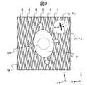
図6および図7は、実施例3の液晶表示パネルにおける偏光部材の構成を説明するための模式図である。
図6は、実施例3の液晶表示パネルにおける偏光部材の吸収軸と透過軸の方向の一例を示す模式平面図である。図7は、偏光部材に設ける下地膜の平面構成の一例を示す模式平面図である。6 and 7 are schematic views for explaining the configuration of the polarizing member in the liquid crystal display panel of Example 3. FIG.
FIG. 6 is a schematic plan view illustrating an example of directions of an absorption axis and a transmission axis of a polarizing member in the liquid crystal display panel of Example 3. FIG. 7 is a schematic plan view illustrating an example of a planar configuration of the base film provided on the polarizing member.
実施例3の液晶表示パネルでは、前述のように、電界無印加時の液晶層6の配向方向ADが画素電極19の帯状電極部の長手方向(y軸方向)に対して角度αだけ傾いている。また、液晶表示パネルは、xy平面でみた平面形状が通常長方形であり、当該長方形は、走査信号線12の長手方向(x軸方向)と平行な辺と、映像信号線14の長手方向(y軸方向)と平行な辺と、で構成される。そのため、第1の偏光部材7および第2の偏光部材8の平面形状も、図6に示したように、x軸方向と平行な辺およびy軸方向と平行な辺により構成される長方形になる。 In the liquid crystal display panel of Example 3, as described above, the alignment direction AD of the
また、実施例3の液晶表示パネルでは、電界無印加時の液晶層6の配向方向ADがy軸方向から角度αだけ傾いている。このとき、電界無印加時の液晶層6の配向方向ADをv軸方向とすると、たとえば、図6に示したように、第1の偏光部材7は透過軸TXがv軸方向と平行になり、第2の偏光部材8は吸収軸AXがv軸方向と平行になるように設けられる。なお、第1の偏光部材7および第2の偏光部材8は、これに限らず、たとえば、第1の偏光部材7の吸収軸AXおよび第2の偏光部材8の透過軸TXがv軸方向と平行になるように設けてもよい。 In the liquid crystal display panel of Example 3, the alignment direction AD of the
したがって、第1の基材1aの表面に第1の偏光部材7を形成するときには、たとえば、図7に示すように、第1の基材1aにおける端辺(y軸方向)に対して角度αだけ傾いたv軸方向がストライプ方向となるように下地膜2を形成する。なお、図7は、第1の基材1aを、偏光層を形成する面の上から見た平面図であり、図4に示した平面図とは左右が反転している。このようにすると、偏光層を形成する面は、u軸方向の表面エネルギーUu(接触角θu)が、v軸方向の表面エネルギーUv(接触角θv)よりも大きくなる。そのため、偏光層材料を塗布したときにあらかじめ定めた一方向(v軸方向)に流動しやすくなり、色素がv軸方向に配向しやすくなる。Therefore, when the first
また、図示は省略するが、第2の基材1bの表面に第2の偏光部材8を形成するときには、たとえば、第2の基材1bの端辺(x軸方向)に対して角度αだけ傾いたu軸方向がストライプ方向となるように下地膜2を形成する。このようにすると、偏光層を形成する面は、v軸方向の表面エネルギーUv(接触角θv)が、u軸方向の表面エネルギーUu(接触角θu)よりも大きく。そのため、偏光層材料を塗布したときにあらかじめ定めた一方向(u軸方向)に流動しやすくなり、色素がu軸方向に配向しやすくなる。Although illustration is omitted, when the second
第1の偏光部材7および第2の偏光部材8の構成を、実施例1または実施例2で説明した構成にした場合、それぞれの偏光部材において二色性が向上し、透過率およびコントラスト比が向上することはもちろんである。また、第1の偏光部材7および第2の偏光部材8における光の回折や干渉の影響による透過率およびコントラスト比の低下を抑制できることももちろんである。そのため、実施例3の液晶表示パネルを有する液晶表示装置は、透過率およびコントラスト比が向上する。 When the configurations of the first
図8は、実施例3の液晶表示パネルにおける画素の平面構成の別の一例を示す模式平面図である。 FIG. 8 is a schematic plan view illustrating another example of the planar configuration of the pixels in the liquid crystal display panel according to the third embodiment.
実施例3の液晶表示パネルにおける画素の平面構成の一例として図4に挙げた構成は、画素電極19の帯状電極部の長手方向がy軸方向と平行であった。しかしながら、画素電極19の帯状電極部は、これに限らず、たとえば、図8に示すように屈曲した形状であってもよい。この構成の場合、y軸方向における帯状電極部の屈曲位置を境界BLとして、境界BLより上の領域と下の領域では、電界Eの方向が反転する。そのため、電界無印加時の液晶層6の配向方向ADをy軸方向に設定すると、電界Eが印加されたときに、境界BLより上の領域の液晶分子は反時計回りに回転し、下の領域の液晶分子は時計回りに回転する。このように電界印加時の液晶分子の回転方向が逆になる領域が一画素内にあると、たとえば、視野角特性が向上する。 In the configuration shown in FIG. 4 as an example of the planar configuration of the pixel in the liquid crystal display panel of Example 3, the longitudinal direction of the strip electrode portion of the
このような液晶表示パネルに第1の偏光部材7および第2の偏光部材8を設ける場合は、たとえば、第1の偏光部材7における下地膜2のストライプ方向をy軸方向、第2の偏光部材8における下地膜2のストライプ方向をx軸方向にすればよい。 When the first
以上、本発明を、前記実施例に基づき具体的に説明したが、本発明は、前記実施例に限定されるものではなく、その要旨を逸脱しない範囲において、種々変更可能であることはもちろんである。 The present invention has been specifically described above based on the above-described embodiments. However, the present invention is not limited to the above-described embodiments, and various modifications can be made without departing from the scope of the present invention. is there.
たとえば、実施例3では、液晶表示パネルの一例として、IPS−Pro方式の液晶表示パネルを挙げたが、本発明は、これに限らず、他の液晶駆動方式(たとえば、TN方式やVA方式など)の液晶表示パネルにも適用できることはもちろんである。 For example, in the third embodiment, an IPS-Pro liquid crystal display panel is given as an example of the liquid crystal display panel. However, the present invention is not limited to this, and other liquid crystal driving methods (for example, TN method, VA method, etc.) Of course, it can also be applied to liquid crystal display panels.
また、本発明の偏光板を液晶表示パネルに適用する場合、当該液晶表示パネルは、たとえば、第1の基板4または第2の基板5のいずれか一方の基板にのみ偏光部材を設ける構成あってもよいことはもちろんである。このような液晶表示パネルでは、通常、第2の基板5にのみ偏光部材を設け、第2の基板5側から液晶表示パネルに入射した外光の反射率を画素毎に独立して制御することで映像や画像を表示する。 When the polarizing plate of the present invention is applied to a liquid crystal display panel, the liquid crystal display panel has a configuration in which a polarizing member is provided only on one of the
また、実施例1乃至実施例3では、基材1の表面に下地膜2および偏光層3を直接形成しているが、これに限らず、たとえば、基材1の表面に1層または2層以上の位相差膜を設け、当該位相差膜の上に下地膜2および偏光層3を形成してもよいことはもちろんである。またさらに、偏光層3の上に、当該偏光層3を保護するための保護膜を形成してもよいことは、言うまでもない。 Moreover, in Example 1 thru | or Example 3, although the
1,1a,1b 基材
2 下地膜
2a,2b (下地膜2の)ライン
3 偏光層
4 第1の基板
5 第2の基板
6 液晶層
7,8 偏光部材
9 下地層
10 半導体膜
11 第1の絶縁層
12 走査信号線
13 第2の絶縁層
14 映像信号線
15 ソース-ドレイン電極
16 第3の絶縁層
17 共通電極
18 第4の絶縁層
19 画素電極
20,24 配向膜
21 ブラックマトリクス
22 カラーフィルタ
23 平坦化層DESCRIPTION OF
Claims (9)
Translated fromJapanese前記偏光層における前記基材と対向する面には、前記偏光層が第1の材料と接している第1の領域と、前記偏光層が第2の材料と接している第2の領域と、があり、かつ、
前記第1の領域と前記第2の領域とがストライプ状に存在し、
前記基材と前記偏光層との間には、第1の材料でなる領域と第2の材料でなる領域がストライプ状に存在している一体の下地膜があり、
前記下地膜の前記偏光層に面した表面は平坦であり、
前記下地膜の前記第1の材料と前記第2の材料とは、特性基の割合、置換基の割合、官能基の割合、および母化合物の割合のうちの1つ以上が異なることを特徴とする偏光板。A polarizing plate having a polarizing layer formed on a substrate,
Wherein the substrate surface opposed to the polarizing layer has a first regionin which the polarizing layer is in contact with the first material, and a second regionin which the polarizing layer is in contact with the second material, And
The first region and the second region exist in a stripe shape,
Between the base material and the polarizing layer, there is anintegral base film in which a region made of the first material and a region made of the second material exist in a stripe shape,
The surface of the base film facing the polarizing layer is flat,
The first material and the second material of the base film are different in at least one of a ratio of a characteristic group, a ratio of a substituent, a ratio of a functional group, and a ratio of a mother compound. Polarizing plate.
前記一対の基板のうちの一方の基板は、絶縁性の基材と、前記基材における第1の面の上に形成された薄膜積層体と、前記基材における前記第1の面とは反対側の第2の面の上に形成された請求項1に記載の偏光層とを有することを特徴とする液晶表示装置。A liquid crystal display device having a liquid crystal display panel in which a liquid crystal layer is sandwiched between a pair of substrates,
One of the pair of substrates is opposite to the insulating base material, the thin film stack formed on the first surface of the base material, and the first surface of the base material. A liquid crystal display device comprising: the polarizing layer according to claim 1 formed on a second surface on the side.
Priority Applications (1)
| Application Number | Priority Date | Filing Date | Title |
|---|---|---|---|
| JP2010056940AJP5337751B2 (en) | 2010-03-15 | 2010-03-15 | Polarizing plate and liquid crystal display device |
Applications Claiming Priority (1)
| Application Number | Priority Date | Filing Date | Title |
|---|---|---|---|
| JP2010056940AJP5337751B2 (en) | 2010-03-15 | 2010-03-15 | Polarizing plate and liquid crystal display device |
Publications (2)
| Publication Number | Publication Date |
|---|---|
| JP2011191461A JP2011191461A (en) | 2011-09-29 |
| JP5337751B2true JP5337751B2 (en) | 2013-11-06 |
Family
ID=44796474
Family Applications (1)
| Application Number | Title | Priority Date | Filing Date |
|---|---|---|---|
| JP2010056940AExpired - Fee RelatedJP5337751B2 (en) | 2010-03-15 | 2010-03-15 | Polarizing plate and liquid crystal display device |
Country Status (1)
| Country | Link |
|---|---|
| JP (1) | JP5337751B2 (en) |
Families Citing this family (3)
| Publication number | Priority date | Publication date | Assignee | Title |
|---|---|---|---|---|
| EP2700987B1 (en) | 2012-08-24 | 2017-04-26 | Lumentum Operations LLC | Variable Optical Retarder |
| JP6160198B2 (en)* | 2013-04-17 | 2017-07-12 | 三菱ケミカル株式会社 | Manufacturing method of polarizer |
| WO2016092709A1 (en)* | 2014-12-12 | 2016-06-16 | 住友化学株式会社 | Cyclo-olefin resin film and polarizing plate using this |
Family Cites Families (8)
| Publication number | Priority date | Publication date | Assignee | Title |
|---|---|---|---|---|
| JP4438188B2 (en)* | 2000-06-29 | 2010-03-24 | 大日本印刷株式会社 | Color filter, manufacturing method thereof, and liquid crystal display device |
| JP4051997B2 (en)* | 2002-05-09 | 2008-02-27 | セイコーエプソン株式会社 | Liquid crystal display device and electronic device |
| JP4165167B2 (en)* | 2002-09-27 | 2008-10-15 | セイコーエプソン株式会社 | Illumination device and projection display device |
| JP2005352320A (en)* | 2004-06-11 | 2005-12-22 | Dainippon Printing Co Ltd | Polarizing plate and manufacturing method thereof |
| JP2007163722A (en)* | 2005-12-13 | 2007-06-28 | Epson Imaging Devices Corp | Liquid crystal device, its manufacturing method, optical retardation plate and electronic device |
| KR20070079833A (en)* | 2006-02-03 | 2007-08-08 | 삼성전자주식회사 | Flat panel and polarizer laminate and protective film attached thereto |
| JP2008106107A (en)* | 2006-10-24 | 2008-05-08 | Fujifilm Corp | Light control material |
| JP4695101B2 (en)* | 2007-01-24 | 2011-06-08 | 株式会社 日立ディスプレイズ | Polarizer and liquid crystal display device using the same |
- 2010
- 2010-03-15JPJP2010056940Apatent/JP5337751B2/ennot_activeExpired - Fee Related
Also Published As
| Publication number | Publication date |
|---|---|
| JP2011191461A (en) | 2011-09-29 |
Similar Documents
| Publication | Publication Date | Title |
|---|---|---|
| KR102747116B1 (en) | Optical film and method of manufacturing the same | |
| JP5026538B2 (en) | Display device | |
| KR102652054B1 (en) | Elliptical polarizing plate | |
| KR102710149B1 (en) | Phase difference plate with optical compensation function | |
| JP6401377B2 (en) | Method for producing polarizing plate and decolorizing solution | |
| JP7398868B2 (en) | Composition | |
| WO2019131949A1 (en) | Laminate, method for producing laminate, and image display device | |
| JP7443413B2 (en) | Vertical alignment liquid crystal cured film | |
| JP5337751B2 (en) | Polarizing plate and liquid crystal display device | |
| KR20160027603A (en) | Polarizing plate, image display device, and method of producing polarizing plate | |
| JP2008233448A (en) | Manufacturing method of wire grid polarizer, wire grid polarizer, polarizing plate, and liquid crystal display device | |
| WO2021006068A1 (en) | Long film | |
| KR102695096B1 (en) | Phase difference plate with optical compensation function for flexible display | |
| JPWO2009004746A1 (en) | Liquid crystal display | |
| JP6160198B2 (en) | Manufacturing method of polarizer | |
| JP6017212B2 (en) | Optical system, liquid crystal element, and method of manufacturing liquid crystal element | |
| JP2022182619A (en) | Optical element, laminate, display device, method for manufacturing optical element | |
| WO2019159886A1 (en) | Composition |
Legal Events
| Date | Code | Title | Description |
|---|---|---|---|
| A621 | Written request for application examination | Free format text:JAPANESE INTERMEDIATE CODE: A621 Effective date:20111102 | |
| A977 | Report on retrieval | Free format text:JAPANESE INTERMEDIATE CODE: A971007 Effective date:20121019 | |
| A131 | Notification of reasons for refusal | Free format text:JAPANESE INTERMEDIATE CODE: A131 Effective date:20121113 | |
| A521 | Request for written amendment filed | Free format text:JAPANESE INTERMEDIATE CODE: A523 Effective date:20121227 | |
| A131 | Notification of reasons for refusal | Free format text:JAPANESE INTERMEDIATE CODE: A131 Effective date:20130305 | |
| A521 | Request for written amendment filed | Free format text:JAPANESE INTERMEDIATE CODE: A523 Effective date:20130501 | |
| TRDD | Decision of grant or rejection written | ||
| A01 | Written decision to grant a patent or to grant a registration (utility model) | Free format text:JAPANESE INTERMEDIATE CODE: A01 Effective date:20130726 | |
| A61 | First payment of annual fees (during grant procedure) | Free format text:JAPANESE INTERMEDIATE CODE: A61 Effective date:20130805 | |
| R150 | Certificate of patent or registration of utility model | Ref document number:5337751 Country of ref document:JP Free format text:JAPANESE INTERMEDIATE CODE: R150 Free format text:JAPANESE INTERMEDIATE CODE: R150 | |
| R250 | Receipt of annual fees | Free format text:JAPANESE INTERMEDIATE CODE: R250 | |
| R250 | Receipt of annual fees | Free format text:JAPANESE INTERMEDIATE CODE: R250 | |
| R250 | Receipt of annual fees | Free format text:JAPANESE INTERMEDIATE CODE: R250 | |
| R250 | Receipt of annual fees | Free format text:JAPANESE INTERMEDIATE CODE: R250 | |
| R250 | Receipt of annual fees | Free format text:JAPANESE INTERMEDIATE CODE: R250 | |
| R250 | Receipt of annual fees | Free format text:JAPANESE INTERMEDIATE CODE: R250 | |
| LAPS | Cancellation because of no payment of annual fees |