JP5335992B2 - Thermocouple assembly with protected thermocouple junction - Google Patents
Thermocouple assembly with protected thermocouple junctionDownload PDFInfo
- Publication number
- JP5335992B2 JP5335992B2JP2012509857AJP2012509857AJP5335992B2JP 5335992 B2JP5335992 B2JP 5335992B2JP 2012509857 AJP2012509857 AJP 2012509857AJP 2012509857 AJP2012509857 AJP 2012509857AJP 5335992 B2JP5335992 B2JP 5335992B2
- Authority
- JP
- Japan
- Prior art keywords
- thermocouple
- support member
- sheath
- line
- assembly
- Prior art date
- Legal status (The legal status is an assumption and is not a legal conclusion. Google has not performed a legal analysis and makes no representation as to the accuracy of the status listed.)
- Active
Links
Images


Classifications
- G—PHYSICS
- G01—MEASURING; TESTING
- G01K—MEASURING TEMPERATURE; MEASURING QUANTITY OF HEAT; THERMALLY-SENSITIVE ELEMENTS NOT OTHERWISE PROVIDED FOR
- G01K7/00—Measuring temperature based on the use of electric or magnetic elements directly sensitive to heat ; Power supply therefor, e.g. using thermoelectric elements
- G01K7/02—Measuring temperature based on the use of electric or magnetic elements directly sensitive to heat ; Power supply therefor, e.g. using thermoelectric elements using thermoelectric elements, e.g. thermocouples
- G01K7/04—Measuring temperature based on the use of electric or magnetic elements directly sensitive to heat ; Power supply therefor, e.g. using thermoelectric elements using thermoelectric elements, e.g. thermocouples the object to be measured not forming one of the thermoelectric materials
Landscapes
- Physics & Mathematics (AREA)
- General Physics & Mathematics (AREA)
- Measuring Temperature Or Quantity Of Heat (AREA)
- Chemical Vapour Deposition (AREA)
Description
Translated fromJapanese本発明は、温度測定デバイスに関し、より具体的には本発明は、半導体処理で使用する熱電対アッセンブリに関する。The present invention relates to temperature measuring devices, and more particularly, the invention relates to thermocouple assemblies for use in semiconductor processing.
半導体処理チャンバは、基板の表面または表面上に様々な物質層を堆積するために使用される。処理チャンバは、低温処理、高温処理、またはその高温処理と低温処理の両方の組み合わせに使用されることができる。シリコンウェハなどの1つまたは複数の基板やワークは、処理チャンバ内のワーク支持体上に配置される。基板及びワーク支持体の双方は所望の温度に加熱される。典型的な化学蒸着(“CVD”)処理ステップでは、反応ガスが各加熱された基板上を通過し、それによって、CVD反応は、基板表面に反応ガスの反応物質の薄層を堆積する。また、処理は、原子層堆積(“ALD”)、プラズマ拡大原子層堆積(“PEALD”)、減圧CVD(“RPCVD”)又は基板上に材料の薄層を堆積させるための他のプロセスを含む。その後の工程を経て、これらの層は、集積回路に作られ、基板の大きさ及び回路の複雑さに応じて数十から数千又は何百万もの統合されたデバイスに作られる。Semiconductor processing chambers are used to deposit various material layers on or on the surface of a substrate. The processing chamber can be used for low temperature processing, high temperature processing, or a combination of both high temperature processing and low temperature processing. One or more substrates or workpieces such as silicon wafers are placed on a workpiece support in the processing chamber. Both the substrate and the workpiece support are heated to the desired temperature. In a typical chemical vapor deposition ("CVD") processing step, a reactive gas passes over each heated substrate, whereby the CVD reaction deposits a thin layer of reactive gas reactants on the substrate surface. Processing also includes atomic layer deposition (“ALD”), plasma enhanced atomic layer deposition (“PEALD”), low pressure CVD (“RPCVD”), or other processes for depositing a thin layer of material on a substrate. . Through subsequent steps, these layers are made into integrated circuits and into tens to thousands or even millions of integrated devices depending on the size of the substrate and the complexity of the circuit.
様々なプロセスパラメータは、得られた堆積層の高品質を確保するために慎重に制御する必要がある。そのような重要なパラメータは、各処理ステップ中の基板の温度である。CVD中、例えば、成膜ガスが基板上に薄い層を堆積させるために特定の温度で反応する。温度は、基板の表面全体にわたって大きく変化する場合、堆積層は、不均一になるかあるいは完成した基板の表面に使用不能の領域につながる可能性の欠陥を有する。したがって、反応ガスが処理チャンバに導入されている間、基板温度が安定して均一であることが重要である。Various process parameters need to be carefully controlled to ensure high quality of the resulting deposited layer. Such an important parameter is the temperature of the substrate during each processing step. During CVD, for example, the deposition gas reacts at a specific temperature to deposit a thin layer on the substrate. If the temperature varies greatly across the surface of the substrate, the deposited layer has defects that can become non-uniform or lead to unusable areas on the finished substrate surface. Therefore, it is important that the substrate temperature be stable and uniform while the reaction gas is introduced into the processing chamber.
同様に、他の熱処理中に基板全体の温度の不均一性や不安定性は、基板の表面上に生じる構造の均一性に影響を与える。温度制御が重要になる他の処理は、酸化、窒化、ドーパント拡散、スパッタ堆積、フォトリソグラフィー、ドライエッチング、プラズマプロセス、および高温アニールを含むがこれに限定しない。Similarly, temperature non-uniformity or instability across the substrate during other heat treatments affects the structural uniformity that occurs on the surface of the substrate. Other processes where temperature control is important include, but are not limited to, oxidation, nitridation, dopant diffusion, sputter deposition, photolithography, dry etching, plasma processes, and high temperature annealing.
処理される基板近傍の又は処理される基板に隣接する様々な位置で温度を測定するための方法及びシステムが知られている。一般的に、熱電対は、処理される基板の近くの様々な場所に配置されており、これらの熱電対は、基板の表面全体にわたってより均一な温度を提供することを支援するためにコントローラに作動的に接続される。例えば、バンビルゼンに発行された米国特許第6121061は、基板を囲む様々なポイントで温度を測定する複数のセンサを開示し、基板の前端近くに、後縁近くに、基板の側面に隣接して、及びそれらの中央近くの基板の下方に配置された熱電対を含む。Methods and systems are known for measuring temperature at various locations near oradjacent to the substrate being processed. In general, thermocouples are located at various locations near the substrate being processed, and these thermocouples provide a controller to assist in providing a more uniform temperature across the surface of the substrate. Operatively connected. For example, U.S. Pat.No. 6,212,061 issued to Van Bilzen discloses a plurality of sensors that measure temperature at various points surrounding a substrate, near the front edge of the substrate, near the trailing edge, adjacent to the side of the substrate, And thermocouples disposed below the substrate near their center.
半導体処理チャンバで使用されている熱電対は、通常、反応室内へ導入されるガス及び反応体からそれと共に配置された熱電対ワイヤを保護するための細長いシースを有する。また、熱電対は、通常、シースの長さを拡張し、それらがそれらの間に熱電対を形成するように異なる金属で形成された一対のワイヤを収容するように構成された支持部材を含む。より短い寿命は、スループット又は所定の時間にわたって処理されるワークの数が品質の重要な指標及びツール全体の所有コストである製造のより頻繁な休止時間を必要とするので、熱電対の寿命は、半導体処理ツールで重要である。したがって、熱電対は温度や圧力の周期的な変化に耐えることができることが重要である。短縮熱電対の寿命に関連する典型的な課題は、断線と一貫性のない温度測定を含む。熱電対の一貫性のない温度測定は、シースの測定チップに対するワイヤの接合(すなわち、熱電対の接点)の一貫性のない場所から生じる。ジャンクションの位置が変化すると、温度測定の精度と一貫性が減少する。熱電対で障害が発生したと考えられる場合の一例は、測定温度が正確でない場合、または測定から測定まで一貫性がないときである。反応チャンバは、その後、一時中止され、障害が発生した熱電対が取り除かれ、ツールの休止時間が収益性を低下させ、ツールの所有コストを増大する。従って、シースに対するジャンクションの移動を防止するためにジャンクションが配置されている一貫性のある位置を提供する熱電対の設計が必要である。Thermocouples used in semiconductor processing chambers typically have an elongate sheath to protect the thermocouple wires placed therewith from gases and reactants introduced into the reaction chamber. Thermocouples also typically include a support member configured to extend the length of the sheath and accommodate a pair of wires formed of different metals so that they form a thermocouple between them. . The shorter lifetime requires more frequent downtime of production, where throughput or the number of workpieces processed over a given time is an important indicator of quality and the cost of ownership of the entire tool, so the lifetime of the thermocouple is Important in semiconductor processing tools. Therefore, it is important that the thermocouple can withstand periodic changes in temperature and pressure. Typical challenges associated with shortened thermocouple life include temperature measurements that are inconsistent with wire breaks. Thermocouple inconsistent temperature measurements result from inconsistent locations of wire bonding (ie, thermocouple contacts) to the sheath measurement tip. Changing the position of the junction reduces the accuracy and consistency of the temperature measurement. An example of when a thermocouple is considered to have failed is when the measured temperature is not accurate or when there is inconsistency from measurement to measurement. The reaction chamber is then suspended, the failed thermocouple is removed, tool downtime decreases profitability, and tool ownership costs increase. Therefore, there is a need for a thermocouple design that provides a consistent location where the junction is located to prevent movement of the junction relative to the sheath.
必要性は、ジャンクションとシースとの間の間隙が続いて生産される熱電対間で容易に繰り返し可能であるように容易に製造可能なシースの測定チップから離間されたガード付きジャンクションを含む温度検知熱電対のために存在する。本発明の一態様では、反応器内の温度を測定するための熱電対アッセンブリが提供される。熱電対アッセンブリは、シースの遠位端に配置された測定チップを有するシースを含む。また、熱電対アッセンブリは、支持部材を含む。支持部材の少なくとも一部分がシース内に収容される。第1線及び第2線が異なる金属で形成され、支持部材内に収容される。第1線及び第2線の各端部は互いに融合されてそれらの間に熱電対ジャンクションを形成する。凹部領域が支持部材の遠位端に形成され、支持部材の遠位端がシース内に収容される。熱電対ジャンクションは、凹部領域のベースに接触して配置される。What is needed is a temperature sensing that includes a guarded junction spaced from an easily manufacturable sheath measuring tip so that the gap between the junction and the sheath is easily repeatable between subsequently produced thermocouples. Present for thermocouples. In one aspect of the invention, a thermocouple assembly is provided for measuring the temperature in the reactor. The thermocouple assembly includes a sheath having a measurement tip disposed at the distal end of the sheath. The thermocouple assembly also includes a support member. At least a portion of the support member is housed within the sheath. The first line and the second line are formed of different metals and are accommodated in the support member. The ends of the first line and the second line are fused together to form athermocouple junction therebetween. A recessed region is formed at the distal end of the support member, and the distal end of the support member is received within the sheath.The thermocouple junction is placed incontact with the base of the recessed area.
本発明の他の態様では、化学蒸着反応器内の温度を測定するための熱電対アッセンブリが提供される。熱電対アッセンブリは、細長い支持部材を含む。支持部材は、それと共に第1線及び第2線の少なくとも一部分を収容するように構成され、第1線及び第2線は異なる金属で形成される。また、熱電対アッセンブリは、測定チップを有する細長いシースを含む。シースは、支持部材の遠位端が測定チップでシースの内面と接するように支持部材を収容するように構成される。熱電対アッセンブリは、第1線及び第2線の各々の端部を融合することによって形成された熱電対ジャンクションを更に含む。凹部領域は、測定チップに隣接した支持部材の遠位端の中に形成され、熱電対ジャンクションは、シースの測定チップに対して実質的に固定された位置に維持される。In another aspect of the invention, a thermocouple assembly is provided for measuring temperature in a chemical vapor deposition reactor. The thermocouple assembly includes an elongated support member. The support member is configured to accommodate at least a portion of the first line and the second line together with the first line and the second line formed of different metals. The thermocouple assembly also includes an elongated sheath having a measurement tip. The sheath is configured to receive the support member such that the distal end of the support member contacts the inner surface of the sheath at the measurement tip. The thermocouple assembly further includes athermocouple junction formed by fusing the ends of each of the first and second wires. A recessed area is formed in the distal end of the support member adjacent to the measurement tip and thethermocouple junction is maintained in a substantially fixed position relative to the measurement tip of the sheath.
本発明のさらに他の態様では、半導体処理反応器で使用するための温度制御システムが提供される。温度制御システムは、反応器内に配置された少なくとも一つの熱要素を含む。また、温度制御システムは、少なくとも一つの熱要素に作動的に接続されたコントローラを含み、コントローラは、少なくとも一つの熱要素を制御するように構成される。さらに、温度制御システムは、反応器内に配置された少なくとも一つの温度センサを含み、温度センサは、コントローラに温度データを提供するためにコントローラに作動的に接続される。少なくとも一つの温度センサは、熱電対アッセンブリであり、熱電対アッセンブリは、シースの遠位端に配置された測定チップを有するシースを含む。また、熱電対アッセンブリは、支持部材を含み、支持部材の少なくとも一部分がシース内に収容される。また、熱電対アッセンブリは、異なる金属で形成された第1線及び第2線を含み、第1線及び第2線の一部分が支持部材内に収容される。第1線及び第2線の各端部が互いに融合されてそれらの間に熱電対ジャンクションを形成する。凹部領域は、支持部材の遠位端に形成され、支持部材の遠位端は、シースの測定チップと接する。熱電対ジャンクションは、シースの測定チップに対して実質的に固定された位置に配置される。In yet another aspect of the invention, a temperature control system for use in a semiconductor processing reactor is provided. The temperature control system includes at least one thermal element disposed within the reactor. The temperature control system also includes a controller operatively connected to the at least one thermal element, the controller configured to control the at least one thermal element. In addition, the temperature control system includes at least one temperature sensor disposed within the reactor, the temperature sensor being operatively connected to the controller to provide temperature data to the controller. The at least one temperature sensor is a thermocouple assembly, the thermocouple assembly including a sheath having a measurement tip disposed at the distal end of the sheath. The thermocouple assembly also includes a support member, and at least a portion of the support member is housed within the sheath. The thermocouple assembly includes a first line and a second line formed of different metals, and a part of the first line and the second line is accommodated in the support member. The ends of the first line and the second line are fused together to form athermocouple junction therebetween. A recessed area is formed at the distal end of the support member, which contacts the measurement tip of the sheath.The thermocouple junction is located at a substantially fixed position relative to the measurement tip of the sheath.
本発明の利点は、図示によって示され説明された本発明の実施形態の以下の説明から当業者に明らかになるであろう。実現されるように、本発明は、他の及び異なる実施形態が可能であり、その詳細は様々な点で変更が可能である。従って、図面及び説明は、本質的に例示し、制限的ではないとみなされる。Advantages of the present invention will become apparent to those skilled in the art from the following description of embodiments of the invention shown and described by way of illustration. As will be realized, the invention is capable of other and different embodiments, and its details are capable of modifications in various respects. Accordingly, the drawings and descriptions are to be regarded as illustrative in nature and not restrictive.
図1を参照すると、半導体基板を処理するための化学蒸着(“CVD”)反応器10の例示的な実施形態が示される。図示の実施形態は、単一の基板で水平方向に流れる冷壁反応器であるが、本明細書中に記載された熱電対概念は、半導体処理反応器の他のタイプに使用されると共に、正確な温度センサを必要とする他の非半導体処理アプリケーションで使用されることを当業者に理解されるべきである。CVD反応器10は、反応空間14を画定する反応チャンバ12と、反応チャンバ12の両側に配置された熱要素16と、基板支持構造18とを含む。反応チャンバ12は、反応空間14の中に反応ガスを導入するインレット20と、そこを通じて反応ガスとプロセスの副産物が反応空間14を出るアウトレット22を有する細長い部材である。実施形態では、反応チャンバ12は、透明な石英で形成されている。反応チャンバ12は、その中の堆積プロセスに対して実質的に非反応性であるのに十分な他の材料で形成されることができることを当業者によって理解されるべきである。Referring to FIG. 1, an exemplary embodiment of a chemical vapor deposition (“CVD”)
熱要素16は、図1に示されるように、上バンクと下バンクを形成する。熱要素16は、同じバンク内で隣接する熱要素16に対して離間して配向される。実施形態では、上バンクの熱要素16は、下バンクの熱要素16に対して実質的に垂直に配向される。熱要素16は、反応チャンバ12の壁によってかなり吸収することなく反応チャンバ12に放射エネルギを提供する。熱要素16は、処理される基板及び基板支持構造18の部分によって吸収される放射熱を提供するように構成される。The
基板支持構造18は、図1に示すように、その上に基板24が配置される基板ホルダ28と、サセプタ支持部材30とを含む。サセプタ支持部材30は、反応チャンバ12の下壁に依存するチューブ34を通じて下方に延びるシャフト32に接続される。モータ(図示せず)は、シャフト32を回転するように構成され、それによって、対応するように基板ホルダ28と基板24を回転する。実施形態では、基板ホルダ28は、シリコンカーバイド(SiC)被覆の黒鉛で形成され、サセプタ支持部材30は、透明な石英で形成される。基板支持機構18の部材が、反応チャンバ12の中に導入されたプロセスガスに関して実質的に不活性であり処理される基板24を支持するのに十分な材料で形成できることを当業者によって理解されるべきである。As shown in FIG. 1, the
図1−2に示すように、複数の温度センサは、基板24と、基板24の近くの様々な場所で温度を測定するための基板ホルダ28とに隣接して配置される。図示の実施形態では、温度センサは、基板ホルダ28の下面に形成された盲目の空洞内に配置された中央温度センサ36、先端温度センサ38、後端温度センサ40、及び少なくとも一方側端の温度センサ42を含む。先端温度センサ38及び後端温度センサ40は、反応空間14内のガスの流れの方向Aに対して基板24の前端及び後端に隣接して配置される。温度センサは、温度センサのチップを囲むローカライズされた領域で温度を測定するように構成される。CVD反応器10の温度制御システム44は、処理される基板24に隣接して配置された複数の温度センサ36、38、40、42を含み、温度センサは、コントローラ46に垂直な位置で温度データを提供する温度コントローラ46に作動的に接続される。コントローラ46は、基板24に隣接して配置された少なくとも一つの熱要素16に作動的に接続される。温度コントローラ46は、処理される基板24全体にわたってほぼ均一な温度分布を維持するために温度センサが提供するデータに応じて熱要素(複数の熱要素)16に供給されるエネルギを調整するように構成されている。温度制御システム44は、コントローラ46にデータを提供するためのさまざまな場所に配置された任意の数の温度センサを含むことができることを当業者によって理解されるべきである。As shown in FIG. 1-2, the plurality of temperature sensors are disposed adjacent to the substrate 24 and a
実施形態では、温度制御システム44で使用される温度センサは熱電対アッセンブリ48である。他の温度センサ36、38、40、42は、光高温計、当該分野で公知の熱電対及びそれらの組み合わせとして形成されることを当業者によって理解されるべきである。図3−4に示すように、熱電対アッセンブリの典型的な実施形態は、一般的に周知であり、シース50、支持部材52、カラー54、第1線56、第2線58、スプリング60、カップアッセンブリ62及びプラグ64を含む。シース50は、長手方向軸線を有する実質的に円筒形の細長い部材である。シース50は、温度測定が望まれる位置に隣接して配置されるように構成された測定チップを含む。また、支持部材52は、長手方向軸線を有する実質的に円筒形の細長い部材であり、支持部材52の一部分がシース50内に収容される。支持部材52は、あらゆるタイプのセラミック又は周期的温度変化及び熱電対アッセンブリ48がさらされる温度領域に耐えるのに十分な他の材料で形成されることができる。熱電対アッセンブリ48は、中央温度センサ36、先端温度センサ38、後端温度センサ40及び側端温度センサ42として使用されることができる。熱電対アッセンブリ48は、正確な温度センサが必要とされている他のアプリケーションで使用されることを当業者に理解されるべきである。図示の熱電対アッセンブリ48は、実質的に線形であるが、熱電対アッセンブリ48は、熱電対アッセンブリ48のチップが処理される基板又は処理される基板を支持する基板支持28に隣接した特に所望の位置に配置されるのを許容するのに十分な形状に形成されることができることを当業者に理解されるべきである。In an embodiment, the temperature sensor used in the
熱電対アッセンブリ48は、図4に示すように、第1線56と第2線58とを含み、第1線56及び第2線58は、異なる金属で形成される。実施形態では、第1線56は、プラチナで形成され、第2線58は、13%のロジウムを有するプラチナの合金で形成されている。第1線56及び第2線58は、それの間に熱電対を形成するのに十分な異なる材料で形成されることができることを当業者に理解されるべきである。第1線56及び第2線58は、支持部材52の長手方向軸線に沿って支持部材52の中心を通って形成された対応する穴68の中に収容される。第1線56及び第2線58の各々の一部は、シース50の測定チップ66に隣接して支持部材52の端部を超えて延びる。従来の熱電対アッセンブリでは、図4に示すように、第1線56及び第2線58の部分は、ビーズを形成するために互いに融合された測定チップ66又は熱電対ジャンクション70に隣接して支持部材52の端部を超えて延びる。スプリング60は、測定チップ66で熱電対の接点70とシース50の内面との間で一定の接触を確実にするように構成されている。スプリング60が一般的に、熱電対ジャンクション70をシース50と接触した状態に維持するために中央温度センサ36として使用された熱電対アッセンブリに使用されるが、スプリングは、前端、後端、又は側端の温度センサ38、40、42で使用した熱電対アッセンブリに必要ではないことを当業者に理解されるべきである。As shown in FIG. 4, the
熱電対ジャンクション70と熱電対アッセンブリ48温度を測定する位置との間の距離は、熱電対アッセンブリ48の設計の重要な特性である。熱電対アッセンブリ48を製造する工程では、測定チップ66内の熱電対ジャンクション70の位置が熱電対から熱電対まで実質的に一定であることが重要である。スプリング60は、支持部材52に一体に取り付けられたカラー54上にスプリング力を及ぼすように構成され、カラー54にかけられたスプリング力は、カラー54を測定チップ66の方に付勢し、熱電対ジャンクション70と測定チップ66との一定の接触を確実にする。以前の周知の熱電対アッセンブリの組み立て中、熱電対ジャンクション70は摺動し又は測定チップ66内でオフセットになり、それによって、熱電対アッセンブリ48によって測定された温度の精度が低下する。さらに、反応チャンバ12(図1)内の熱サイクル中に、温度変化は、熱電対ジャンクション70が摺動又は測定チップ66内でオフセットさせる。さらに、熱電対ジャンクション70は、シース50内で支持部材52の端部を超えて延びるので、熱電対ジャンクション70と第1線56及び第2線58の一部分とは、CVD反応器内で熱要素16にさらされる。この熱要素16に対する直接的な露呈は、反応チャンバ12の熱サイクル中で熱電対ジャンクション70と第1線56及び第2線58を損傷させる。さらに、熱電対ジャンクション70は支持部材52の端部を超えて延びるので熱電対ジャンクション70と第1線56及び第2線58は、反応チャンバ内で熱要素16にさらされる。このように、熱電対ジャンクション70がさらされる高温と組み合わせでスプリング60の圧縮力は、時間をかけて熱電対ジャンクション70の形状を変形する。この変形は、熱電対によって測定された温度の精度に悪影響を与える。The distance between the
改善された熱電対アッセンブリ100の例示的な実施形態が図5に示される。熱電対アッセンブリ100は、シース102、支持部材104、カラー106、第1線108、第2線110、スプリング112、カップアッセンブリ114及びプラグ116を含む。実施形態では、シース102は、長手方向軸線を有する実施的に円筒形の細長い部材である。シース102は、温度測定が望まれる位置に隣接して配置されるように構成された測定チップ118を含む。実施形態では、シース102は、透明な石英で形成されている。熱電対アッセンブリ100が反応チャンバ12内に収められる温度範囲に十分に耐えることができる材料で形成されることを当業者は理解されるべきである。また、支持部材104は、長手方向軸線を有する実質的に円筒形の細長い部材であり、支持部材104の一部分がシース102内に収容される。支持部材104は、シース102内に収容されるのに十分な形状として形成されることを当業者に理解されるべきである。支持部材104は、セラミック又は周期的温度変化及び熱電対アッセンブリ100がさらされる温度領域に耐えるのに十分な他の材料で形成されることができる。熱電対アッセンブリ100は、図2に示すように、中央温度センサ36、先端温度センサ38、後端温度センサ40及び側端温度センサ42として使用されることができる。熱電対アッセンブリ100は、正確な温度センサが必要とされている他のアプリケーションで使用されることを当業者に理解されるべきである。図示の熱電対アッセンブリ100は、実質的に線形であるが、熱電対アッセンブリ100は、熱電対アッセンブリ100のチップ118が特に所望の位置に配置されるのを許容するのに十分な形状に形成されることができることを当業者に理解されるべきである。An exemplary embodiment of an
熱電対アッセンブリ100は、図5に示すように、第1線108と第2線110とを含み、第1線108及び第2線110は、異なる金属で形成される。実施形態では、第1線108は、プラチナで形成され、第2線110は、13%のロジウムを有するプラチナの合金で形成されている。第1線108及び第2線110は、それの間に熱電対を形成するのに十分な異なる材料で形成されることができることを当業者に理解されるべきである。第1線108及び第2線110は、支持部材104の長手方向軸線に沿って支持部材104の中心を通って形成された対応する穴120の中に収容される。As shown in FIG. 5, the
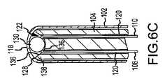
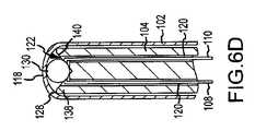
実施形態では、図6A−6Dに示すように、測定チップ118に隣接した支持部材104のチップは、凹部領域122を形成する。図6Aに示された実施形態では、凹部領域122は、傾斜した側面124を含む。傾斜した側面124は、傾斜した側面124が支持部材104の遠位端から離れる方向に延びるように支持部材104の長手方向軸線の方に内方に傾斜する。ベース126は、支持部材104の端部において凹部領域122に底面を形成する。ベース126は、実質的に平面である。凹部領域122は、支持部材104の端部の中に概ね頭を切断された円錐形状のくぼみを形成する。凹部領域122は、支持部材104の遠位端を形成する縁部128によって囲まれる。実施形態では、傾斜した側面124は、縁部128が実質的に平らな棚を形成するように支持部材104の外面から半径方向内方に離間される。他の実施形態では、傾斜した側面124は、支持部材104の遠位端が環状のリングを形成するように支持部材104の外面(図示せず)から延びる。実施形態では、凹部領域122は、支持部材104を成形するときに形成されることができる。他の実施形態では、凹部領域122は、支持部材104の一部分を切断又は粉砕することによって形成されることができる。凹部領域122は、熱電対ジャンクション130を保護するために構成された側壁138を提供するのに十分な方法によって形成されることを当業者によって理解されるべきである。In the embodiment, as shown in FIGS. 6A-6D, the tip of the
組み立て中に、図6Aに示されるように、第1線108及び第2線110の一部分は凹部領域122の中にそれらの対応する穴120から延びる。第1線108及び第2線110のさらされた部分は、ビーズ又は熱電対ジャンクション130を形成するために互いに融合される。熱電対ジャンクション130は、凹部領域122のベース126と接触して配置され、傾斜した側面124によって保護される。ひとたび熱電対ジャンクション130が形成されると、支持部材104は、縁部128が測定チップ118でシース102の内面と接するまでシース102の中に挿入される。組み立てられると、熱電対ジャンクション130は、シース102の測定チップ118に対して実質的に固定した位置に配置される。During assembly, portions of the
図6A−6Dは、シース102の内面と接する熱電対ジャンクション130を図示し、図6Eは、シースに対して離間された関係に配置された熱電対ジャンクション130を図示する。熱電対アッセンブリ100は、熱電対ジャンクション130がシース102と接するか隣接するが、熱電対ジャンクション130がスプリング112からスプリング力に従わないで測定チップ118に対して実質的に固定された場所又は位置に存在するように組み立てられることができることを当業者によって理解されるべきである。例えば、実施形態では、熱電対ジャンクション130は、熱電対ジャンクション130が測定チップ118でシース102の内面と接するように凹部領域122内に配置される。しかしながら、スプリング112は、シースの内面に対して支持部材104を付勢するので、熱電対ジャンクション130は、静止し、スプリング112からシース102に対するスプリング力を受けない。他の実施形態では、ジャンクションは、シース112の内面に隣接して離間配置されたように配置される。6A-6D illustrate the
図6Bに示す熱電対アッセンブリ100の他の実施形態では、凹部領域122は、側面132とベース134とを含む。側面132は、支持部材104の長手方向軸線に対して実質的に平行なように支持部材104の厚さの中に遠位端から延びる。ベース134は、支持部材104の端部で凹部領域122の底面を形成する。ベース134は、側面132に対して90度に形成された平面である。凹部領域122は、支持部材104の端部の中に概ね円筒形のくぼみを形成する。凹部領域122は、支持部材104の遠位端を形成する縁部128によって囲まれる。実施形態では、側面132は、縁部128が実質的に平らな棚を形成するように支持部材104の外面から半径方向内方に離間される。In another embodiment of the
組み立て中に、図6Bに示されるように、第1線108及び第2線110の一部分は凹部領域122の中にそれらの対応する穴120から延びる。第1線108及び第2線110のさらされた部分は、ビーズ又は熱電対ジャンクション130を形成するために互いに融合される。熱電対ジャンクション130は、凹部領域122のベース126と接触して配置され、側面132によって保護される。ひとたび熱電対ジャンクション130が形成されると、支持部材104は、縁部128が測定チップ118でシース102の内面と接するまでシース102の中に挿入される。組み立てられると、熱電対ジャンクション130は、シース102の測定チップ118に対して実質的に固定した位置に配置される。During assembly, portions of the
図6Cに示す実施形態では、凹部領域122は傾斜した面136を含む。傾斜した面136は、傾斜した面136が支持部材104の遠位端から離れる方向に延びるように支持部材104の長手方向軸線の方に内方に傾斜する。凹部領域122は、支持部材104の端部の中に概ね半球状のくぼみを形成する。凹部領域122は、支持部材104の遠位端を形成する縁部によって囲まれる。実施形態では、傾斜した側面136は、縁部128が実質的に平らな棚を形成するように支持部材104の外面から半径方向内方に離間される。他の実施形態では、傾斜した側面136は、支持部材104の遠位端が環状のリングを形成するように支持部材104の外面から延びる。実施形態では、凹部領域122は、支持部材104を成形するときに形成されることができる。他の実施形態では、凹部領域122は、支持部材104の一部分を切断又は粉砕することによって形成されることができる。凹部領域122は、熱電対ジャンクション130を保護するために構成された側壁138を提供するのに十分な方法によって形成されることを当業者によって理解されるべきである。In the embodiment shown in FIG. 6C, the recessed
組み立て中に、図6Cに示されるように、第1線108及び第2線110の一部分は凹部領域122の中にそれらの対応する穴120から延びる。第1線108及び第2線110のさらされた部分は、ビーズ又は熱電対ジャンクション130を形成するために互いに融合される。熱電対ジャンクション130は、凹部領域122のベース126と接触して配置され、傾斜した面136によって保護される。ひとたび熱電対ジャンクション130が形成されると、支持部材104は、縁部128が測定チップ118でシース102の内面と接するまでシース102の中に挿入される。組み立てられると、熱電対ジャンクション130は、シース102の測定チップ118に対して実質的に固定した位置に配置される。During assembly, portions of the
図6Dに示す実施形態では、凹部領域122は傾斜した面140を含む。傾斜した面140は、傾斜した面140が支持部材104の遠位端から離れる方向に延び、傾斜した面140が支持部材104の長手方向軸線上に又はその軸線に実質的に近傍にポイントを形成するように支持部材104の長手方向軸線の方に内方に傾斜する。凹部領域122は、支持部材104の端部の中に概ねV形状又は円錐形のくぼみを形成する。凹部領域122は、支持部材104の遠位端を形成する縁部128によって囲まれる。実施形態では、傾斜した面140は、縁部128が実質的に平らな棚を形成するように支持部材104の外面から半径方向内方に離間される。他の実施形態では、縁部128が半径方向に延びる厚さがほとんどない又は全くない棚を形成するように傾斜した側面136は支持部材104の外面から延びる。実施形態では、凹部領域122は、支持部材104の端部の中に傾斜した表面140を切断又は粉砕することによって形成されることができる。凹部領域122は、熱電対ジャンクション130を保護するために構成された側壁138を提供するのに十分な方法によって形成されることを当業者によって理解されるべきである。In the embodiment shown in FIG. 6D, the recessed
組み立て中に、図6Dに示されるように、第1線108及び第2線110の一部分は凹部領域122の中にそれらの対応する穴120から延びる。第1線108及び第2線110のさらされた部分は、ビーズ又は熱電対ジャンクション130を形成するために互いに融合される。熱電対ジャンクション130は、傾斜した面140が半径方向内方に延びるように傾斜した面140によって形成されたポイントに隣接して配置される。ひとたび熱電対ジャンクション130が形成されると、支持部材104は、縁部128が測定チップ118でシース102の内面と接するまでシース102の中に挿入される。組み立てられると、熱電対ジャンクション130は、シース102の測定チップ118に対して実質的に固定した位置に配置される。During assembly, portions of the
図6A−6Dに示された凹部領域122は、支持部材104の長手方向軸線に沿って実質的に対称なくぼみであるように示される。しかしながら、支持部材104の端部は、凹部領域122を含む必要はなく、その長手方向軸線を中心にして対称である必要はない。例えば、図6Eは、支持部材の端部が、支持部材の傾斜した面142が実質的に平らで支持部材104の長手方向軸線にたいして傾斜して形成されるように切り捨てられた実施形態を示す。それに隣接して熱電対ジャンクション130が平らに形成された支持部材104の端部がくぼみ又は凹部領域を含み、あるいは、熱電対ジャンクション130が測定チップ118でシース102の内面に対して相対的に配置されるのを許容するように形状づけられることを当業者に理解されるべきである。The recessed
実施形態では、熱電対ジャンクション130は、図6A−6Eに示されるように、測定チップ118でシース102の内面と接合関係である。支持部材104の側壁138とシース102との間の接触は、測定チップ118に対して熱電対ジャンクション130を付勢するスプリング力が実質的にないようにスプリング112によって支持部材104にかけられたスプリング力のほぼすべてを吸収する。スプリング力が支持部材104とシース102との間の接触によって吸収されるので、熱電対ジャンクション130は、スリップ又は変形しないで測定チップ118と接触して実質的に固定された位置にある。他の実施形態では、図6Eに示されるように、熱電対ジャンクション130は、測定チップ118でシース102の内面に隣接して配置され、それによって、熱電対ジャンクション130とシース102との間に少しの間隙を提供する。熱電対ジャンクション130は測定チップ118でシース102の内面と接触して又は内面から離れる方向に離間され、支持部材104とシース102との接触は、熱電対から熱電対まで測定チップ118に対して実施的に固定された位置に熱電対ジャンクション130が存在するのを許容するように、測定チップ118に対して熱電対ジャンクション130を典型的に付勢するスプリング力を減少又は排除するように構成されることを当業者に理解されるべきである。In an embodiment, the
図6Eに示された実施形態では、熱電対ジャンクション130が測定チップ118でシース102の内面から離間される距離は、約1mmである。他の実施形態では、熱電対ジャンクション130が測定チップ118でシース102の内面から離間される距離は、約0.5mmである。さらに他の実施形態では、熱電対ジャンクション130が測定チップ118でシース102の内面から離間される距離は、約5mmより小さく、より具体的には約1mmより小さい。他の実施形態では、熱電対ジャンクション130が測定チップ118でシース102の内面から離間される距離は、約0.1mm乃至1.5mmである。熱電対ジャンクション130との間の離間された距離は、あらゆる距離にすることができるが、離間された距離は、各熱電対アッセンブリ100に対する熱電対ジャンクション130と測定チップ118との間の離間された距離が実質的に同じであるように続いて製造される熱電対間のメンテナンスを容易にする必要がある。In the embodiment shown in FIG. 6E, the distance that the
図6A−6Dに示されるように、熱電対ジャンクション130は、支持部材104に形成された凹部領域122のベースに配置される。凹部領域122のベースに配置されると、スプリング112が熱電対アッセンブリ100の測定チップ118の方に支持部材104を付勢するようにスプリング112は熱電対ジャンクション130に圧縮力を伝えない。一般的に周知の中央熱電対では、スプリングは、ジャンクションと測定チップとの間に接触を維持するためにジャンクションを測定チップと接触状態に付勢する。しかしながら、ジャンクションにかけられたこのスプリング力は、シースの内面に対してジャンクションを圧縮させ、典型的に、熱電対の温度測定のエラー及び早期故障を生じるジャンクションの変形を生じる。これに対して、本発明の改善された熱電対アッセンブリ100の熱電対ジャンクション130は、スプリング112からのスプリング力によって支持部材104とシース102との間の一定の圧縮のもとに熱電対ジャンクション130があった場合に生じる熱電対ジャンクション130が測定チップ118に対して摺動せず又はオフセットにならないように、測定チップ118でシース102と接触してあるいはシース102に隣接して、凹部領域122内に実質的に固定された位置にあることができる。熱電対ジャンクション130は、シース102に対して摺動しない又はオフセットにならないで支持部材104の凹部領域122内に実質的に固定された位置にあるので、熱電対アッセンブリ100によって提供された温度データは、一貫性がある。さらに、シース102に対する熱電対ジャンクション130の不慮の摺動又はオフセットを防止することは、熱電対アッセンブリ100の温度データが反応チャンバ12内の多くの熱サイクル後に一貫性があるため、熱電対アッセンブリ100の寿命を増加させる。As shown in FIGS. 6A-6D, the
凹部領域122は、熱電対アッセンブリ100の支持部材104の遠位端の中に形成された概ねくぼんだ領域である。図6A−6Dに示す実施形態では、凹部領域122は、支持部材104の長手方向軸線を中心に実質的に対称である。凹部領域122は、支持部材104の長手方向軸線を中心に非対称にすることができることを当業者は理解されるべきである。また、凹部領域122の形状は、凹部領域122のベースに配置された熱電対ジャンクション130を実質的に囲むのに十分な形状にすることができることを当業者は理解されるべきである。凹部領域122によって形成されたくぼみは、側壁138が完全にジャンクションを囲むように支持部材104の遠位端の方に凹部領域122のベースから延びる側壁138を形成する。さらに、シース102の測定チップ118に対して実質的に固定された位置に熱電対ジャンクション130を維持することに加えて、凹部領域122の側壁138は、熱要素16(図1)によって生じた放射熱から熱電対ジャンクション130の保護を提供する。従って、熱電対ジャンクション130は、直接放射線から遮蔽され、それによって、熱電対ジャンクション130及び凹部領域122内の第1線108、第2線110のさらされた部分への損傷を減少する。The recessed
図6A−6Eに示されるように、シース102の測定チップ118は、シース102の遠位端にある曲がったチップとして形成される。代替的な実施形態では、測定チップ118は、シース102の側壁138に実質的に垂直に形成されることができる。測定チップ118の形状は、あらゆる形状にすることができることを当業者は理解されるべきである。凹部領域122のベースの実質的に固定された位置に形成されたジャンクション及び測定チップ118での支持部材104の縁部128とシース102の内面との間の接触は、熱電対ジャンクション130が続いて起こる熱電対100の製造中測定チップ118に対して実質的に同じ位置に配置されるのを許容する。熱電対ジャンクション130は、凹部領域122内に実質的に固定された位置に維持されるので、熱電対ジャンクション130と測定チップ118との間の関係は実質的に一定である。製造業の熱電対における重要な変数の一つは、シース102の測定チップ118に対し実質的に固定された位置に熱電対ジャンクション130を一貫して維持する能力である。続いて製造される熱電対の測定チップ118に対する熱電対ジャンクション130の実質的に一貫性のある位置を提供する能力は、製造中又は反応チャンバインサートの熱サイクル中にジャンクションが摺動し、圧縮された平坦になり、あるいは支持部材の遠位端でオフセットになる一般的に周知の熱電対以上の改善を提供する。As shown in FIGS. 6A-6E, the
本発明の好適な実施形態について説明したが、本発明は限定されず、変形は本発明から逸脱しないでなされることができる。本発明の範囲は添付の特許請求の範囲によって定義され、クレームの意味内に入るすべてのデバイス、プロセス、方法は、文字どおりに又は等価的にそこに包含されることが意図される。Although preferred embodiments of the present invention have been described, the present invention is not limited and modifications can be made without departing from the invention. The scope of the present invention is defined by the appended claims, and all devices, processes, methods that fall within the meaning of the claims are intended to be included literally or equivalently therein.
Claims (21)
Translated fromJapaneseシースの遠位端に配置された測定チップを有するシースと、
支持部材であって、支持部材の少なくとも一部分がシース内に収容される支持部材と、
異なる金属で形成された第1線及び第2線であって、第1線及び第2線の一部分が支持部材内に収容され、第1線及び第2線の各端部が互いに融合されてそれらの間に熱電対ジャンクションを形成する、第1線及び第2線と、
支持部材の遠位端に形成された凹部領域であって、支持部材の遠位端がシースと接し、熱電対ジャンクションが凹部領域のベースに接触して配置された、凹部領域とを備える、熱電対アッセンブリ。A thermocouple assembly for measuring a temperature in a chemical vapor deposition reactor,
A sheath having a measuring tip disposed at the distal end of the sheath;
A support member wherein at least a portion of the support member is housed within the sheath;
A first line and a second line made of different metals, wherein a part of the first line and the second line is accommodated in the support member, and ends of the first line and the second line are fused together. A first line and a second line forming athermocouple junction between them;
A recessed region formed at a distal end of the support member, wherein the distal end of the support member is incontact with the sheath and athermocouple junction is disposed incontact with the base of the recessed region. Versus assembly.
熱電対ジャンクションは、シースの測定チップから固定された離間された距離で配置される熱電対アッセンブリ。The thermocouple assembly of claim 1, wherein
The thermocouple junction is located at a fixed spaced distance from the measurement tip of the sheath.
熱電対ジャンクションとシースの測定チップとの間の固定された離間された距離は、5mmよりも小さい熱電対アッセンブリ。The thermocouple assembly of claim 2, wherein
A thermocouple assembly in which the fixed spaced distance between thethermocouple junction and the sheath measurement tip is less than 5 mm.
熱電対ジャンクションとシースの測定チップとの間の固定された離間された距離は、1mmよりも小さい熱電対アッセンブリ。The thermocouple assembly of claim 2, wherein
A thermocouple assembly in which the fixed spaced distance between thethermocouple junction and the sheath measurement tip is less than 1 mm.
熱電対ジャンクションは、シースの測定チップと接する熱電対アッセンブリ。The thermocouple assembly of claim 1, wherein
A thermocouple junction is a thermocouple assembly that contacts the measuring tip of the sheath.
縁部が支持部材の遠位端で凹部領域の回りに形成される熱電対アッセンブリ。The thermocouple assembly of claim 1, wherein
A thermocouple assembly in which an edge is formed around the recessed area at the distal end of the support member.
縁部は、支持部材の長手方向軸線に対して実質的に垂直に延びる棚である熱電対アッセンブリ。The thermocouple assembly of claim 6, wherein
The thermocouple assembly, wherein the edge is a shelf extending substantially perpendicular to the longitudinal axis of the support member.
縁部は、測定チップでシースの内面と接する熱電対アッセンブリ。The thermocouple assembly of claim 6, wherein
The edge is a thermocouple assembly that contacts the inner surface of the sheath at the measurement tip.
熱電対ジャンクションは、凹部領域のベースに対して実質的に固定した位置に維持される熱電対アッセンブリ。The thermocouple assembly of claim 1, wherein
A thermocouple assembly in which the thermocouple junction is maintained in a substantially fixed position relative to the base of the recessed area.
凹部領域の周りに形成された側壁を更に備え、側壁は、熱電対ジャンクションを保護する熱電対アッセンブリ。The thermocouple assembly of claim 1, wherein
Further comprising a sidewall formed around the recessed area, the side wall is a thermocouple assembly for protecting athermocouple junction.
凹部領域は、実質的に半球状のくぼみを形成する熱電対アッセンブリ。The thermocouple assembly of claim 1, wherein
The recessed area is a thermocouple assembly that forms a substantially hemispherical depression.
凹部領域は、実質的に円筒形のくぼみを形成する熱電対アッセンブリ。The thermocouple assembly of claim 1, wherein
The recessed area is a thermocouple assembly that forms a substantially cylindrical recess.
凹部領域は、先端が切り取られた円錐形のくぼみを形成する熱電対アッセンブリ。The thermocouple assembly of claim 1, wherein
The recessed area is a thermocouple assembly that forms a conical depression with a truncated tip.
凹部領域は、円錐形のくぼみを形成する熱電対アッセンブリ。The thermocouple assembly of claim 1, wherein
The recessed area is a thermocouple assembly that forms a conical depression.
第1線は、プラチナで形成され、第2線は、約13%のロジウムを有するプラチナの合金で形成される熱電対アッセンブリ。The thermocouple assembly of claim 1, wherein
The first wire is formed of platinum and the second wire is a thermocouple assembly formed of a platinum alloy having about 13% rhodium.
それと共に第1線及び第2線の少なくとも一部分を収容するように構成された細長い支持部材であって、第1線及び第2線は異なる金属で形成された細長い支持部材と、
測定チップを有する細長いシースであって、支持部材の遠位端が測定チップでシースの内面と接するように支持部材を収容するように構成された細長いシースと、
第1線及び第2線の各々の端部を融合することによって形成された熱電対ジャンクションと、
細長い支持部材の遠位端の中に形成された凹部領域であって、熱電対ジャンクションが凹部領域のベースに接触して配置されると共にシースの測定チップに対して実質的に固定された位置に維持される、凹部領域とを有する熱電対アッセンブリ。A thermocouple assembly for measuring a temperature in a chemical vapor deposition reactor,
And an elongate support member configured to receive at least a portion of the first line and the second line therewith, wherein the first line and the second line are formed of different metals;
An elongate sheath having a measurement tip, the elongate sheath configured to receive the support member such that the distal end of the support member contacts the inner surface of the sheath at the measurement tip;
Athermocouple junction formed by fusing the ends of each of the first and second wires;
A recessed area formed in the distal end of the elongated support member, wherein thethermocouple junction isdisposed in contact with the base of the recessed area and is in a substantially fixed position relative to the measurement tip of the sheath.A thermocouple assemblyhaving a recessed region that is maintained.
反応器内に配置された少なくとも一つの熱要素と、
少なくとも一つの熱要素に作動的に接続され、少なくとも一つの熱要素を制御するように構成されたコントローラと、
コントローラに温度データを提供するためにコントローラに作動的に接続された、反応器内に配置された少なくとも一つの温度センサであって、熱電対アッセンブリを備える少なくとも一つの温度センサとを備え、
熱電対アッセンブリは、
シースの遠位端に配置された測定チップを有するシースと、
支持部材であって、支持部材の少なくとも一部分がシース内に収容される支持部材と、
異なる金属で形成された第1線及び第2線であって、第1線及び第2線の一部分が支持部材内に収容され、第1線及び第2線の各端部が互いに融合されてそれらの間に熱電対ジャンクションを形成する、第1線及び第2線と、
支持部材の遠位端に形成された凹部領域であって、支持部材の遠位端がシースの測定チップと接し、熱電対ジャンクションが凹部領域のベースに接触して配置されると共にシースの測定チップに対して実質的に固定された位置に配置される、凹部領域とを有する温度制御システム。A temperature control system for use in a semiconductor processing reactor comprising:
At least one thermal element disposed in the reactor;
A controller operatively connected to the at least one thermal element and configured to control the at least one thermal element;
At least one temperature sensor disposed in the reactor operatively connected to the controller for providing temperature data to the controller, the thermosensor assembly comprising at least one temperature sensor;
The thermocouple assembly is
A sheath having a measuring tip disposed at the distal end of the sheath;
A support member wherein at least a portion of the support member is housed within the sheath;
A first line and a second line made of different metals, wherein a part of the first line and the second line is accommodated in the support member, and ends of the first line and the second line are fused together. A first line and a second line forming athermocouple junction between them;
A recess region formed at the distal end of the support member, wherein the distal end of the support member isin contact with the sheath measurement tip, and thethermocouple junction isdisposed in contact with the base of the recess region, and the sheath measurement tip And a recessed area disposed in a substantially fixed position relative to the temperature control system.
凹部領域は、熱電対ジャンクションを囲む側壁を形成し、それによって、少なくとも一つの熱要素からの放射エネルギから熱電対ジャンクションを保護する温度制御システム。The temperature control system according to claim 17, wherein
Recessed region forms a side wall surrounding thethermocouple junction, thereby the temperature control system to protect thethermocouple junction from the radiant energy from at least one heat element.
凹部領域は、支持部材の遠位端の実質的に半球状のくぼみとして形成される温度制御システム。The temperature control system according to claim 17, wherein
A temperature control system in which the recessed area is formed as a substantially hemispherical depression at the distal end of the support member.
凹部領域は、支持部材の遠位端の実質的に円筒形のくぼみとして形成される温度制御システム。The temperature control system according to claim 17, wherein
A temperature control system in which the recessed area is formed as a substantially cylindrical recess at the distal end of the support member.
支持部材の遠位端で凹部領域の周りに形成された縁部を更に備え、縁部は、熱電対ジャンクションと測定チップとの間に離間した距離を提供するためにシースの内面と接する温度制御システム。The temperature control system according to claim 17, wherein
Further comprising an edge formed around the recessed area at the distal end of the support member, the edge being in contact with the inner surface of the sheath to provide a spaced distance between thethermocouple junction and the measurement tip system.
Applications Claiming Priority (3)
| Application Number | Priority Date | Filing Date | Title |
|---|---|---|---|
| US12/436,300US8382370B2 (en) | 2009-05-06 | 2009-05-06 | Thermocouple assembly with guarded thermocouple junction |
| US12/436,300 | 2009-05-06 | ||
| PCT/US2010/033244WO2010129428A1 (en) | 2009-05-06 | 2010-04-30 | Thermocouple assembly with guarded thermocouple junction |
Publications (2)
| Publication Number | Publication Date |
|---|---|
| JP2012526282A JP2012526282A (en) | 2012-10-25 |
| JP5335992B2true JP5335992B2 (en) | 2013-11-06 |
Family
ID=43050380
Family Applications (1)
| Application Number | Title | Priority Date | Filing Date |
|---|---|---|---|
| JP2012509857AActiveJP5335992B2 (en) | 2009-05-06 | 2010-04-30 | Thermocouple assembly with protected thermocouple junction |
Country Status (4)
| Country | Link |
|---|---|
| US (2) | US8382370B2 (en) |
| JP (1) | JP5335992B2 (en) |
| TW (1) | TWI489526B (en) |
| WO (1) | WO2010129428A1 (en) |
Families Citing this family (370)
| Publication number | Priority date | Publication date | Assignee | Title |
|---|---|---|---|---|
| US8123405B2 (en)* | 2006-06-22 | 2012-02-28 | Bae Systems Information Solutions Inc. | Programmable circuit for drift compensation |
| US20090052498A1 (en)* | 2007-08-24 | 2009-02-26 | Asm America, Inc. | Thermocouple |
| US10378106B2 (en) | 2008-11-14 | 2019-08-13 | Asm Ip Holding B.V. | Method of forming insulation film by modified PEALD |
| US8262287B2 (en) | 2008-12-08 | 2012-09-11 | Asm America, Inc. | Thermocouple |
| US9394608B2 (en) | 2009-04-06 | 2016-07-19 | Asm America, Inc. | Semiconductor processing reactor and components thereof |
| US9297705B2 (en) | 2009-05-06 | 2016-03-29 | Asm America, Inc. | Smart temperature measuring device |
| US8100583B2 (en)* | 2009-05-06 | 2012-01-24 | Asm America, Inc. | Thermocouple |
| US8382370B2 (en) | 2009-05-06 | 2013-02-26 | Asm America, Inc. | Thermocouple assembly with guarded thermocouple junction |
| US8802201B2 (en) | 2009-08-14 | 2014-08-12 | Asm America, Inc. | Systems and methods for thin-film deposition of metal oxides using excited nitrogen-oxygen species |
| US8734012B2 (en)* | 2009-08-21 | 2014-05-27 | Therm-O-Disc, Incorporated | Temperature sensor |
| US9312155B2 (en) | 2011-06-06 | 2016-04-12 | Asm Japan K.K. | High-throughput semiconductor-processing apparatus equipped with multiple dual-chamber modules |
| US10364496B2 (en) | 2011-06-27 | 2019-07-30 | Asm Ip Holding B.V. | Dual section module having shared and unshared mass flow controllers |
| US10854498B2 (en) | 2011-07-15 | 2020-12-01 | Asm Ip Holding B.V. | Wafer-supporting device and method for producing same |
| US20130023129A1 (en) | 2011-07-20 | 2013-01-24 | Asm America, Inc. | Pressure transmitter for a semiconductor processing environment |
| US9017481B1 (en) | 2011-10-28 | 2015-04-28 | Asm America, Inc. | Process feed management for semiconductor substrate processing |
| EP2700923B1 (en)* | 2012-07-04 | 2017-06-21 | Services Pétroliers Schlumberger | Apparatus for determining fluid characteristics |
| US9659799B2 (en) | 2012-08-28 | 2017-05-23 | Asm Ip Holding B.V. | Systems and methods for dynamic semiconductor process scheduling |
| US10714315B2 (en) | 2012-10-12 | 2020-07-14 | Asm Ip Holdings B.V. | Semiconductor reaction chamber showerhead |
| US20160376700A1 (en) | 2013-02-01 | 2016-12-29 | Asm Ip Holding B.V. | System for treatment of deposition reactor |
| USD702188S1 (en) | 2013-03-08 | 2014-04-08 | Asm Ip Holding B.V. | Thermocouple |
| US9484191B2 (en) | 2013-03-08 | 2016-11-01 | Asm Ip Holding B.V. | Pulsed remote plasma method and system |
| US9589770B2 (en) | 2013-03-08 | 2017-03-07 | Asm Ip Holding B.V. | Method and systems for in-situ formation of intermediate reactive species |
| KR102261013B1 (en)* | 2013-03-14 | 2021-06-03 | 어플라이드 머티어리얼스, 인코포레이티드 | Temperature measurement in multi-zone heater |
| US9240412B2 (en) | 2013-09-27 | 2016-01-19 | Asm Ip Holding B.V. | Semiconductor structure and device and methods of forming same using selective epitaxial process |
| US10683571B2 (en) | 2014-02-25 | 2020-06-16 | Asm Ip Holding B.V. | Gas supply manifold and method of supplying gases to chamber using same |
| US10167557B2 (en) | 2014-03-18 | 2019-01-01 | Asm Ip Holding B.V. | Gas distribution system, reactor including the system, and methods of using the same |
| US11015245B2 (en) | 2014-03-19 | 2021-05-25 | Asm Ip Holding B.V. | Gas-phase reactor and system having exhaust plenum and components thereof |
| US10858737B2 (en) | 2014-07-28 | 2020-12-08 | Asm Ip Holding B.V. | Showerhead assembly and components thereof |
| US9890456B2 (en) | 2014-08-21 | 2018-02-13 | Asm Ip Holding B.V. | Method and system for in situ formation of gas-phase compounds |
| US9657845B2 (en) | 2014-10-07 | 2017-05-23 | Asm Ip Holding B.V. | Variable conductance gas distribution apparatus and method |
| US10941490B2 (en) | 2014-10-07 | 2021-03-09 | Asm Ip Holding B.V. | Multiple temperature range susceptor, assembly, reactor and system including the susceptor, and methods of using the same |
| KR102263121B1 (en) | 2014-12-22 | 2021-06-09 | 에이에스엠 아이피 홀딩 비.브이. | Semiconductor device and manufacuring method thereof |
| US10529542B2 (en) | 2015-03-11 | 2020-01-07 | Asm Ip Holdings B.V. | Cross-flow reactor and method |
| US10276355B2 (en) | 2015-03-12 | 2019-04-30 | Asm Ip Holding B.V. | Multi-zone reactor, system including the reactor, and method of using the same |
| US10728956B2 (en)* | 2015-05-29 | 2020-07-28 | Watlow Electric Manufacturing Company | Resistive heater with temperature sensing power pins |
| CN107852836B (en)* | 2015-06-17 | 2020-08-14 | 巴斯威技术有限公司 | Device, method and system for bus duct power distribution |
| US10458018B2 (en) | 2015-06-26 | 2019-10-29 | Asm Ip Holding B.V. | Structures including metal carbide material, devices including the structures, and methods of forming same |
| US10600673B2 (en) | 2015-07-07 | 2020-03-24 | Asm Ip Holding B.V. | Magnetic susceptor to baseplate seal |
| US9960072B2 (en) | 2015-09-29 | 2018-05-01 | Asm Ip Holding B.V. | Variable adjustment for precise matching of multiple chamber cavity housings |
| US10186437B2 (en)* | 2015-10-05 | 2019-01-22 | Lam Research Corporation | Substrate holder having integrated temperature measurement electrical devices |
| US10211308B2 (en) | 2015-10-21 | 2019-02-19 | Asm Ip Holding B.V. | NbMC layers |
| US10373794B2 (en) | 2015-10-29 | 2019-08-06 | Lam Research Corporation | Systems and methods for filtering radio frequencies from a signal of a thermocouple and controlling a temperature of an electrode in a plasma chamber |
| US10322384B2 (en) | 2015-11-09 | 2019-06-18 | Asm Ip Holding B.V. | Counter flow mixer for process chamber |
| US11139308B2 (en) | 2015-12-29 | 2021-10-05 | Asm Ip Holding B.V. | Atomic layer deposition of III-V compounds to form V-NAND devices |
| US10529554B2 (en) | 2016-02-19 | 2020-01-07 | Asm Ip Holding B.V. | Method for forming silicon nitride film selectively on sidewalls or flat surfaces of trenches |
| US10468251B2 (en) | 2016-02-19 | 2019-11-05 | Asm Ip Holding B.V. | Method for forming spacers using silicon nitride film for spacer-defined multiple patterning |
| US10501866B2 (en) | 2016-03-09 | 2019-12-10 | Asm Ip Holding B.V. | Gas distribution apparatus for improved film uniformity in an epitaxial system |
| US10343920B2 (en) | 2016-03-18 | 2019-07-09 | Asm Ip Holding B.V. | Aligned carbon nanotubes |
| US9892913B2 (en) | 2016-03-24 | 2018-02-13 | Asm Ip Holding B.V. | Radial and thickness control via biased multi-port injection settings |
| US10190213B2 (en) | 2016-04-21 | 2019-01-29 | Asm Ip Holding B.V. | Deposition of metal borides |
| US10865475B2 (en) | 2016-04-21 | 2020-12-15 | Asm Ip Holding B.V. | Deposition of metal borides and silicides |
| US10367080B2 (en) | 2016-05-02 | 2019-07-30 | Asm Ip Holding B.V. | Method of forming a germanium oxynitride film |
| US10032628B2 (en) | 2016-05-02 | 2018-07-24 | Asm Ip Holding B.V. | Source/drain performance through conformal solid state doping |
| KR102592471B1 (en) | 2016-05-17 | 2023-10-20 | 에이에스엠 아이피 홀딩 비.브이. | Method of forming metal interconnection and method of fabricating semiconductor device using the same |
| US11453943B2 (en) | 2016-05-25 | 2022-09-27 | Asm Ip Holding B.V. | Method for forming carbon-containing silicon/metal oxide or nitride film by ALD using silicon precursor and hydrocarbon precursor |
| US10388509B2 (en) | 2016-06-28 | 2019-08-20 | Asm Ip Holding B.V. | Formation of epitaxial layers via dislocation filtering |
| US9859151B1 (en) | 2016-07-08 | 2018-01-02 | Asm Ip Holding B.V. | Selective film deposition method to form air gaps |
| US10612137B2 (en) | 2016-07-08 | 2020-04-07 | Asm Ip Holdings B.V. | Organic reactants for atomic layer deposition |
| US10714385B2 (en) | 2016-07-19 | 2020-07-14 | Asm Ip Holding B.V. | Selective deposition of tungsten |
| KR102354490B1 (en) | 2016-07-27 | 2022-01-21 | 에이에스엠 아이피 홀딩 비.브이. | Method of processing a substrate |
| KR102532607B1 (en) | 2016-07-28 | 2023-05-15 | 에이에스엠 아이피 홀딩 비.브이. | Substrate processing apparatus and method of operating the same |
| US10395919B2 (en) | 2016-07-28 | 2019-08-27 | Asm Ip Holding B.V. | Method and apparatus for filling a gap |
| US9887082B1 (en) | 2016-07-28 | 2018-02-06 | Asm Ip Holding B.V. | Method and apparatus for filling a gap |
| US9812320B1 (en) | 2016-07-28 | 2017-11-07 | Asm Ip Holding B.V. | Method and apparatus for filling a gap |
| CN106289558A (en)* | 2016-08-19 | 2017-01-04 | 宁波中家院电器技术有限公司 | A kind of method measuring microwave-oven-heating uniformity is improved |
| KR102613349B1 (en) | 2016-08-25 | 2023-12-14 | 에이에스엠 아이피 홀딩 비.브이. | Exhaust apparatus and substrate processing apparatus and thin film fabricating method using the same |
| US10410943B2 (en) | 2016-10-13 | 2019-09-10 | Asm Ip Holding B.V. | Method for passivating a surface of a semiconductor and related systems |
| US10643826B2 (en) | 2016-10-26 | 2020-05-05 | Asm Ip Holdings B.V. | Methods for thermally calibrating reaction chambers |
| US11532757B2 (en) | 2016-10-27 | 2022-12-20 | Asm Ip Holding B.V. | Deposition of charge trapping layers |
| US10435790B2 (en) | 2016-11-01 | 2019-10-08 | Asm Ip Holding B.V. | Method of subatmospheric plasma-enhanced ALD using capacitively coupled electrodes with narrow gap |
| US10643904B2 (en) | 2016-11-01 | 2020-05-05 | Asm Ip Holdings B.V. | Methods for forming a semiconductor device and related semiconductor device structures |
| US10714350B2 (en) | 2016-11-01 | 2020-07-14 | ASM IP Holdings, B.V. | Methods for forming a transition metal niobium nitride film on a substrate by atomic layer deposition and related semiconductor device structures |
| US10229833B2 (en) | 2016-11-01 | 2019-03-12 | Asm Ip Holding B.V. | Methods for forming a transition metal nitride film on a substrate by atomic layer deposition and related semiconductor device structures |
| US10134757B2 (en) | 2016-11-07 | 2018-11-20 | Asm Ip Holding B.V. | Method of processing a substrate and a device manufactured by using the method |
| KR102546317B1 (en) | 2016-11-15 | 2023-06-21 | 에이에스엠 아이피 홀딩 비.브이. | Gas supply unit and substrate processing apparatus including the same |
| US10340135B2 (en) | 2016-11-28 | 2019-07-02 | Asm Ip Holding B.V. | Method of topologically restricted plasma-enhanced cyclic deposition of silicon or metal nitride |
| KR102762543B1 (en) | 2016-12-14 | 2025-02-05 | 에이에스엠 아이피 홀딩 비.브이. | Substrate processing apparatus |
| US11581186B2 (en) | 2016-12-15 | 2023-02-14 | Asm Ip Holding B.V. | Sequential infiltration synthesis apparatus |
| US11447861B2 (en) | 2016-12-15 | 2022-09-20 | Asm Ip Holding B.V. | Sequential infiltration synthesis apparatus and a method of forming a patterned structure |
| KR102700194B1 (en) | 2016-12-19 | 2024-08-28 | 에이에스엠 아이피 홀딩 비.브이. | Substrate processing apparatus |
| US10269558B2 (en) | 2016-12-22 | 2019-04-23 | Asm Ip Holding B.V. | Method of forming a structure on a substrate |
| US10867788B2 (en) | 2016-12-28 | 2020-12-15 | Asm Ip Holding B.V. | Method of forming a structure on a substrate |
| US11390950B2 (en) | 2017-01-10 | 2022-07-19 | Asm Ip Holding B.V. | Reactor system and method to reduce residue buildup during a film deposition process |
| US10655221B2 (en) | 2017-02-09 | 2020-05-19 | Asm Ip Holding B.V. | Method for depositing oxide film by thermal ALD and PEALD |
| US10468261B2 (en) | 2017-02-15 | 2019-11-05 | Asm Ip Holding B.V. | Methods for forming a metallic film on a substrate by cyclical deposition and related semiconductor device structures |
| US10529563B2 (en) | 2017-03-29 | 2020-01-07 | Asm Ip Holdings B.V. | Method for forming doped metal oxide films on a substrate by cyclical deposition and related semiconductor device structures |
| US10283353B2 (en) | 2017-03-29 | 2019-05-07 | Asm Ip Holding B.V. | Method of reforming insulating film deposited on substrate with recess pattern |
| KR102457289B1 (en) | 2017-04-25 | 2022-10-21 | 에이에스엠 아이피 홀딩 비.브이. | Method for depositing a thin film and manufacturing a semiconductor device |
| US10446393B2 (en) | 2017-05-08 | 2019-10-15 | Asm Ip Holding B.V. | Methods for forming silicon-containing epitaxial layers and related semiconductor device structures |
| US10892156B2 (en) | 2017-05-08 | 2021-01-12 | Asm Ip Holding B.V. | Methods for forming a silicon nitride film on a substrate and related semiconductor device structures |
| US10770286B2 (en) | 2017-05-08 | 2020-09-08 | Asm Ip Holdings B.V. | Methods for selectively forming a silicon nitride film on a substrate and related semiconductor device structures |
| RU174817U1 (en)* | 2017-05-10 | 2017-11-03 | федеральное государственное бюджетное образовательное учреждение высшего образования "Омский государственный университет им. Ф.М. Достоевского" | Microcalorimeter with evacuated measuring cell |
| US10504742B2 (en) | 2017-05-31 | 2019-12-10 | Asm Ip Holding B.V. | Method of atomic layer etching using hydrogen plasma |
| US10886123B2 (en) | 2017-06-02 | 2021-01-05 | Asm Ip Holding B.V. | Methods for forming low temperature semiconductor layers and related semiconductor device structures |
| US12040200B2 (en) | 2017-06-20 | 2024-07-16 | Asm Ip Holding B.V. | Semiconductor processing apparatus and methods for calibrating a semiconductor processing apparatus |
| US11306395B2 (en) | 2017-06-28 | 2022-04-19 | Asm Ip Holding B.V. | Methods for depositing a transition metal nitride film on a substrate by atomic layer deposition and related deposition apparatus |
| US10685834B2 (en) | 2017-07-05 | 2020-06-16 | Asm Ip Holdings B.V. | Methods for forming a silicon germanium tin layer and related semiconductor device structures |
| KR20190009245A (en) | 2017-07-18 | 2019-01-28 | 에이에스엠 아이피 홀딩 비.브이. | Methods for forming a semiconductor device structure and related semiconductor device structures |
| US11018002B2 (en) | 2017-07-19 | 2021-05-25 | Asm Ip Holding B.V. | Method for selectively depositing a Group IV semiconductor and related semiconductor device structures |
| US10541333B2 (en) | 2017-07-19 | 2020-01-21 | Asm Ip Holding B.V. | Method for depositing a group IV semiconductor and related semiconductor device structures |
| US11374112B2 (en) | 2017-07-19 | 2022-06-28 | Asm Ip Holding B.V. | Method for depositing a group IV semiconductor and related semiconductor device structures |
| US10605530B2 (en) | 2017-07-26 | 2020-03-31 | Asm Ip Holding B.V. | Assembly of a liner and a flange for a vertical furnace as well as the liner and the vertical furnace |
| US10590535B2 (en) | 2017-07-26 | 2020-03-17 | Asm Ip Holdings B.V. | Chemical treatment, deposition and/or infiltration apparatus and method for using the same |
| US10312055B2 (en) | 2017-07-26 | 2019-06-04 | Asm Ip Holding B.V. | Method of depositing film by PEALD using negative bias |
| TWI815813B (en) | 2017-08-04 | 2023-09-21 | 荷蘭商Asm智慧財產控股公司 | Showerhead assembly for distributing a gas within a reaction chamber |
| US10770336B2 (en) | 2017-08-08 | 2020-09-08 | Asm Ip Holding B.V. | Substrate lift mechanism and reactor including same |
| US10692741B2 (en) | 2017-08-08 | 2020-06-23 | Asm Ip Holdings B.V. | Radiation shield |
| US11769682B2 (en) | 2017-08-09 | 2023-09-26 | Asm Ip Holding B.V. | Storage apparatus for storing cassettes for substrates and processing apparatus equipped therewith |
| US10249524B2 (en) | 2017-08-09 | 2019-04-02 | Asm Ip Holding B.V. | Cassette holder assembly for a substrate cassette and holding member for use in such assembly |
| US11139191B2 (en) | 2017-08-09 | 2021-10-05 | Asm Ip Holding B.V. | Storage apparatus for storing cassettes for substrates and processing apparatus equipped therewith |
| USD900036S1 (en) | 2017-08-24 | 2020-10-27 | Asm Ip Holding B.V. | Heater electrical connector and adapter |
| US11830730B2 (en) | 2017-08-29 | 2023-11-28 | Asm Ip Holding B.V. | Layer forming method and apparatus |
| US11056344B2 (en) | 2017-08-30 | 2021-07-06 | Asm Ip Holding B.V. | Layer forming method |
| KR102491945B1 (en) | 2017-08-30 | 2023-01-26 | 에이에스엠 아이피 홀딩 비.브이. | Substrate processing apparatus |
| US11295980B2 (en) | 2017-08-30 | 2022-04-05 | Asm Ip Holding B.V. | Methods for depositing a molybdenum metal film over a dielectric surface of a substrate by a cyclical deposition process and related semiconductor device structures |
| KR102401446B1 (en) | 2017-08-31 | 2022-05-24 | 에이에스엠 아이피 홀딩 비.브이. | Substrate processing apparatus |
| US10607895B2 (en) | 2017-09-18 | 2020-03-31 | Asm Ip Holdings B.V. | Method for forming a semiconductor device structure comprising a gate fill metal |
| KR102630301B1 (en) | 2017-09-21 | 2024-01-29 | 에이에스엠 아이피 홀딩 비.브이. | Method of sequential infiltration synthesis treatment of infiltrateable material and structures and devices formed using same |
| US10844484B2 (en) | 2017-09-22 | 2020-11-24 | Asm Ip Holding B.V. | Apparatus for dispensing a vapor phase reactant to a reaction chamber and related methods |
| US10658205B2 (en) | 2017-09-28 | 2020-05-19 | Asm Ip Holdings B.V. | Chemical dispensing apparatus and methods for dispensing a chemical to a reaction chamber |
| US10403504B2 (en) | 2017-10-05 | 2019-09-03 | Asm Ip Holding B.V. | Method for selectively depositing a metallic film on a substrate |
| US10319588B2 (en) | 2017-10-10 | 2019-06-11 | Asm Ip Holding B.V. | Method for depositing a metal chalcogenide on a substrate by cyclical deposition |
| US10923344B2 (en) | 2017-10-30 | 2021-02-16 | Asm Ip Holding B.V. | Methods for forming a semiconductor structure and related semiconductor structures |
| RU181370U1 (en)* | 2017-11-07 | 2018-07-11 | федеральное государственное бюджетное образовательное учреждение высшего образования "Омский государственный университет им. Ф.М. Достоевского" | Microcalorimeter with evacuated measuring cell |
| US10910262B2 (en) | 2017-11-16 | 2021-02-02 | Asm Ip Holding B.V. | Method of selectively depositing a capping layer structure on a semiconductor device structure |
| KR102443047B1 (en) | 2017-11-16 | 2022-09-14 | 에이에스엠 아이피 홀딩 비.브이. | Method of processing a substrate and a device manufactured by the same |
| US11022879B2 (en) | 2017-11-24 | 2021-06-01 | Asm Ip Holding B.V. | Method of forming an enhanced unexposed photoresist layer |
| WO2019103613A1 (en) | 2017-11-27 | 2019-05-31 | Asm Ip Holding B.V. | A storage device for storing wafer cassettes for use with a batch furnace |
| CN111344522B (en) | 2017-11-27 | 2022-04-12 | 阿斯莫Ip控股公司 | Including clean mini-environment device |
| US10290508B1 (en) | 2017-12-05 | 2019-05-14 | Asm Ip Holding B.V. | Method for forming vertical spacers for spacer-defined patterning |
| US10872771B2 (en) | 2018-01-16 | 2020-12-22 | Asm Ip Holding B. V. | Method for depositing a material film on a substrate within a reaction chamber by a cyclical deposition process and related device structures |
| KR102695659B1 (en) | 2018-01-19 | 2024-08-14 | 에이에스엠 아이피 홀딩 비.브이. | Method for depositing a gap filling layer by plasma assisted deposition |
| TWI799494B (en) | 2018-01-19 | 2023-04-21 | 荷蘭商Asm 智慧財產控股公司 | Deposition method |
| USD903477S1 (en) | 2018-01-24 | 2020-12-01 | Asm Ip Holdings B.V. | Metal clamp |
| US11018047B2 (en) | 2018-01-25 | 2021-05-25 | Asm Ip Holding B.V. | Hybrid lift pin |
| US10535516B2 (en) | 2018-02-01 | 2020-01-14 | Asm Ip Holdings B.V. | Method for depositing a semiconductor structure on a surface of a substrate and related semiconductor structures |
| USD880437S1 (en) | 2018-02-01 | 2020-04-07 | Asm Ip Holding B.V. | Gas supply plate for semiconductor manufacturing apparatus |
| US11081345B2 (en) | 2018-02-06 | 2021-08-03 | Asm Ip Holding B.V. | Method of post-deposition treatment for silicon oxide film |
| US10896820B2 (en) | 2018-02-14 | 2021-01-19 | Asm Ip Holding B.V. | Method for depositing a ruthenium-containing film on a substrate by a cyclical deposition process |
| WO2019158960A1 (en) | 2018-02-14 | 2019-08-22 | Asm Ip Holding B.V. | A method for depositing a ruthenium-containing film on a substrate by a cyclical deposition process |
| US10731249B2 (en) | 2018-02-15 | 2020-08-04 | Asm Ip Holding B.V. | Method of forming a transition metal containing film on a substrate by a cyclical deposition process, a method for supplying a transition metal halide compound to a reaction chamber, and related vapor deposition apparatus |
| US10658181B2 (en) | 2018-02-20 | 2020-05-19 | Asm Ip Holding B.V. | Method of spacer-defined direct patterning in semiconductor fabrication |
| KR102636427B1 (en) | 2018-02-20 | 2024-02-13 | 에이에스엠 아이피 홀딩 비.브이. | Substrate processing method and apparatus |
| US10975470B2 (en) | 2018-02-23 | 2021-04-13 | Asm Ip Holding B.V. | Apparatus for detecting or monitoring for a chemical precursor in a high temperature environment |
| US11473195B2 (en) | 2018-03-01 | 2022-10-18 | Asm Ip Holding B.V. | Semiconductor processing apparatus and a method for processing a substrate |
| US11629406B2 (en) | 2018-03-09 | 2023-04-18 | Asm Ip Holding B.V. | Semiconductor processing apparatus comprising one or more pyrometers for measuring a temperature of a substrate during transfer of the substrate |
| US11114283B2 (en) | 2018-03-16 | 2021-09-07 | Asm Ip Holding B.V. | Reactor, system including the reactor, and methods of manufacturing and using same |
| KR102646467B1 (en) | 2018-03-27 | 2024-03-11 | 에이에스엠 아이피 홀딩 비.브이. | Method of forming an electrode on a substrate and a semiconductor device structure including an electrode |
| US10510536B2 (en) | 2018-03-29 | 2019-12-17 | Asm Ip Holding B.V. | Method of depositing a co-doped polysilicon film on a surface of a substrate within a reaction chamber |
| US11230766B2 (en) | 2018-03-29 | 2022-01-25 | Asm Ip Holding B.V. | Substrate processing apparatus and method |
| US11088002B2 (en) | 2018-03-29 | 2021-08-10 | Asm Ip Holding B.V. | Substrate rack and a substrate processing system and method |
| KR102501472B1 (en) | 2018-03-30 | 2023-02-20 | 에이에스엠 아이피 홀딩 비.브이. | Substrate processing method |
| KR102600229B1 (en) | 2018-04-09 | 2023-11-10 | 에이에스엠 아이피 홀딩 비.브이. | Substrate supporting device, substrate processing apparatus including the same and substrate processing method |
| US12025484B2 (en) | 2018-05-08 | 2024-07-02 | Asm Ip Holding B.V. | Thin film forming method |
| TWI811348B (en) | 2018-05-08 | 2023-08-11 | 荷蘭商Asm 智慧財產控股公司 | Methods for depositing an oxide film on a substrate by a cyclical deposition process and related device structures |
| US12272527B2 (en) | 2018-05-09 | 2025-04-08 | Asm Ip Holding B.V. | Apparatus for use with hydrogen radicals and method of using same |
| KR20190129718A (en) | 2018-05-11 | 2019-11-20 | 에이에스엠 아이피 홀딩 비.브이. | Methods for forming a doped metal carbide film on a substrate and related semiconductor device structures |
| KR102596988B1 (en) | 2018-05-28 | 2023-10-31 | 에이에스엠 아이피 홀딩 비.브이. | Method of processing a substrate and a device manufactured by the same |
| US11718913B2 (en) | 2018-06-04 | 2023-08-08 | Asm Ip Holding B.V. | Gas distribution system and reactor system including same |
| TWI840362B (en) | 2018-06-04 | 2024-05-01 | 荷蘭商Asm Ip私人控股有限公司 | Wafer handling chamber with moisture reduction |
| US11286562B2 (en) | 2018-06-08 | 2022-03-29 | Asm Ip Holding B.V. | Gas-phase chemical reactor and method of using same |
| KR102568797B1 (en) | 2018-06-21 | 2023-08-21 | 에이에스엠 아이피 홀딩 비.브이. | Substrate processing system |
| US10797133B2 (en) | 2018-06-21 | 2020-10-06 | Asm Ip Holding B.V. | Method for depositing a phosphorus doped silicon arsenide film and related semiconductor device structures |
| TWI873894B (en) | 2018-06-27 | 2025-02-21 | 荷蘭商Asm Ip私人控股有限公司 | Cyclic deposition methods for forming metal-containing material and films and structures including the metal-containing material |
| KR102854019B1 (en) | 2018-06-27 | 2025-09-02 | 에이에스엠 아이피 홀딩 비.브이. | Periodic deposition method for forming a metal-containing material and films and structures comprising the metal-containing material |
| US10612136B2 (en) | 2018-06-29 | 2020-04-07 | ASM IP Holding, B.V. | Temperature-controlled flange and reactor system including same |
| KR102686758B1 (en) | 2018-06-29 | 2024-07-18 | 에이에스엠 아이피 홀딩 비.브이. | Method for depositing a thin film and manufacturing a semiconductor device |
| US10755922B2 (en) | 2018-07-03 | 2020-08-25 | Asm Ip Holding B.V. | Method for depositing silicon-free carbon-containing film as gap-fill layer by pulse plasma-assisted deposition |
| US10388513B1 (en) | 2018-07-03 | 2019-08-20 | Asm Ip Holding B.V. | Method for depositing silicon-free carbon-containing film as gap-fill layer by pulse plasma-assisted deposition |
| US10767789B2 (en) | 2018-07-16 | 2020-09-08 | Asm Ip Holding B.V. | Diaphragm valves, valve components, and methods for forming valve components |
| US10483099B1 (en) | 2018-07-26 | 2019-11-19 | Asm Ip Holding B.V. | Method for forming thermally stable organosilicon polymer film |
| US11053591B2 (en) | 2018-08-06 | 2021-07-06 | Asm Ip Holding B.V. | Multi-port gas injection system and reactor system including same |
| US10883175B2 (en) | 2018-08-09 | 2021-01-05 | Asm Ip Holding B.V. | Vertical furnace for processing substrates and a liner for use therein |
| US10829852B2 (en) | 2018-08-16 | 2020-11-10 | Asm Ip Holding B.V. | Gas distribution device for a wafer processing apparatus |
| US11430674B2 (en) | 2018-08-22 | 2022-08-30 | Asm Ip Holding B.V. | Sensor array, apparatus for dispensing a vapor phase reactant to a reaction chamber and related methods |
| KR102707956B1 (en) | 2018-09-11 | 2024-09-19 | 에이에스엠 아이피 홀딩 비.브이. | Method for deposition of a thin film |
| US11024523B2 (en) | 2018-09-11 | 2021-06-01 | Asm Ip Holding B.V. | Substrate processing apparatus and method |
| US11049751B2 (en) | 2018-09-14 | 2021-06-29 | Asm Ip Holding B.V. | Cassette supply system to store and handle cassettes and processing apparatus equipped therewith |
| CN110970344B (en) | 2018-10-01 | 2024-10-25 | Asmip控股有限公司 | Substrate holding apparatus, system comprising the same and method of using the same |
| US11232963B2 (en) | 2018-10-03 | 2022-01-25 | Asm Ip Holding B.V. | Substrate processing apparatus and method |
| KR102592699B1 (en) | 2018-10-08 | 2023-10-23 | 에이에스엠 아이피 홀딩 비.브이. | Substrate support unit and apparatuses for depositing thin film and processing the substrate including the same |
| US10847365B2 (en) | 2018-10-11 | 2020-11-24 | Asm Ip Holding B.V. | Method of forming conformal silicon carbide film by cyclic CVD |
| US10811256B2 (en) | 2018-10-16 | 2020-10-20 | Asm Ip Holding B.V. | Method for etching a carbon-containing feature |
| KR102546322B1 (en) | 2018-10-19 | 2023-06-21 | 에이에스엠 아이피 홀딩 비.브이. | Substrate processing apparatus and substrate processing method |
| KR102605121B1 (en) | 2018-10-19 | 2023-11-23 | 에이에스엠 아이피 홀딩 비.브이. | Substrate processing apparatus and substrate processing method |
| USD948463S1 (en) | 2018-10-24 | 2022-04-12 | Asm Ip Holding B.V. | Susceptor for semiconductor substrate supporting apparatus |
| US10381219B1 (en) | 2018-10-25 | 2019-08-13 | Asm Ip Holding B.V. | Methods for forming a silicon nitride film |
| US12378665B2 (en) | 2018-10-26 | 2025-08-05 | Asm Ip Holding B.V. | High temperature coatings for a preclean and etch apparatus and related methods |
| US11087997B2 (en) | 2018-10-31 | 2021-08-10 | Asm Ip Holding B.V. | Substrate processing apparatus for processing substrates |
| KR102748291B1 (en) | 2018-11-02 | 2024-12-31 | 에이에스엠 아이피 홀딩 비.브이. | Substrate support unit and substrate processing apparatus including the same |
| US11572620B2 (en) | 2018-11-06 | 2023-02-07 | Asm Ip Holding B.V. | Methods for selectively depositing an amorphous silicon film on a substrate |
| US11031242B2 (en) | 2018-11-07 | 2021-06-08 | Asm Ip Holding B.V. | Methods for depositing a boron doped silicon germanium film |
| US10847366B2 (en) | 2018-11-16 | 2020-11-24 | Asm Ip Holding B.V. | Methods for depositing a transition metal chalcogenide film on a substrate by a cyclical deposition process |
| US10818758B2 (en) | 2018-11-16 | 2020-10-27 | Asm Ip Holding B.V. | Methods for forming a metal silicate film on a substrate in a reaction chamber and related semiconductor device structures |
| US10559458B1 (en) | 2018-11-26 | 2020-02-11 | Asm Ip Holding B.V. | Method of forming oxynitride film |
| US12040199B2 (en) | 2018-11-28 | 2024-07-16 | Asm Ip Holding B.V. | Substrate processing apparatus for processing substrates |
| US11217444B2 (en) | 2018-11-30 | 2022-01-04 | Asm Ip Holding B.V. | Method for forming an ultraviolet radiation responsive metal oxide-containing film |
| KR102636428B1 (en) | 2018-12-04 | 2024-02-13 | 에이에스엠 아이피 홀딩 비.브이. | A method for cleaning a substrate processing apparatus |
| US11158513B2 (en) | 2018-12-13 | 2021-10-26 | Asm Ip Holding B.V. | Methods for forming a rhenium-containing film on a substrate by a cyclical deposition process and related semiconductor device structures |
| TWI874340B (en) | 2018-12-14 | 2025-03-01 | 荷蘭商Asm Ip私人控股有限公司 | Method of forming device structure, structure formed by the method and system for performing the method |
| CN111413002A (en)* | 2019-01-08 | 2020-07-14 | 日新离子机器株式会社 | Substrate temperature measuring device and semiconductor manufacturing device |
| TWI866480B (en) | 2019-01-17 | 2024-12-11 | 荷蘭商Asm Ip 私人控股有限公司 | Methods of forming a transition metal containing film on a substrate by a cyclical deposition process |
| KR102727227B1 (en) | 2019-01-22 | 2024-11-07 | 에이에스엠 아이피 홀딩 비.브이. | Semiconductor processing device |
| CN111524788B (en) | 2019-02-01 | 2023-11-24 | Asm Ip私人控股有限公司 | Method for forming topologically selective films of silicon oxide |
| KR102626263B1 (en) | 2019-02-20 | 2024-01-16 | 에이에스엠 아이피 홀딩 비.브이. | Cyclical deposition method including treatment step and apparatus for same |
| TWI845607B (en) | 2019-02-20 | 2024-06-21 | 荷蘭商Asm Ip私人控股有限公司 | Cyclical deposition method and apparatus for filling a recess formed within a substrate surface |
| TWI838458B (en) | 2019-02-20 | 2024-04-11 | 荷蘭商Asm Ip私人控股有限公司 | Apparatus and methods for plug fill deposition in 3-d nand applications |
| TWI873122B (en) | 2019-02-20 | 2025-02-21 | 荷蘭商Asm Ip私人控股有限公司 | Method of filling a recess formed within a surface of a substrate, semiconductor structure formed according to the method, and semiconductor processing apparatus |
| TWI842826B (en) | 2019-02-22 | 2024-05-21 | 荷蘭商Asm Ip私人控股有限公司 | Substrate processing apparatus and method for processing substrate |
| KR102782593B1 (en) | 2019-03-08 | 2025-03-14 | 에이에스엠 아이피 홀딩 비.브이. | Structure Including SiOC Layer and Method of Forming Same |
| US11742198B2 (en) | 2019-03-08 | 2023-08-29 | Asm Ip Holding B.V. | Structure including SiOCN layer and method of forming same |
| KR102858005B1 (en) | 2019-03-08 | 2025-09-09 | 에이에스엠 아이피 홀딩 비.브이. | Method for Selective Deposition of Silicon Nitride Layer and Structure Including Selectively-Deposited Silicon Nitride Layer |
| JP2020167398A (en) | 2019-03-28 | 2020-10-08 | エーエスエム・アイピー・ホールディング・ベー・フェー | Door openers and substrate processing equipment provided with door openers |
| KR102809999B1 (en) | 2019-04-01 | 2025-05-19 | 에이에스엠 아이피 홀딩 비.브이. | Method of manufacturing semiconductor device |
| KR20200123380A (en) | 2019-04-19 | 2020-10-29 | 에이에스엠 아이피 홀딩 비.브이. | Layer forming method and apparatus |
| KR20200125453A (en) | 2019-04-24 | 2020-11-04 | 에이에스엠 아이피 홀딩 비.브이. | Gas-phase reactor system and method of using same |
| US11289326B2 (en) | 2019-05-07 | 2022-03-29 | Asm Ip Holding B.V. | Method for reforming amorphous carbon polymer film |
| KR20200130121A (en) | 2019-05-07 | 2020-11-18 | 에이에스엠 아이피 홀딩 비.브이. | Chemical source vessel with dip tube |
| KR20200130652A (en) | 2019-05-10 | 2020-11-19 | 에이에스엠 아이피 홀딩 비.브이. | Method of depositing material onto a surface and structure formed according to the method |
| JP7598201B2 (en) | 2019-05-16 | 2024-12-11 | エーエスエム・アイピー・ホールディング・ベー・フェー | Wafer boat handling apparatus, vertical batch furnace and method |
| JP7612342B2 (en) | 2019-05-16 | 2025-01-14 | エーエスエム・アイピー・ホールディング・ベー・フェー | Wafer boat handling apparatus, vertical batch furnace and method |
| USD947913S1 (en) | 2019-05-17 | 2022-04-05 | Asm Ip Holding B.V. | Susceptor shaft |
| USD975665S1 (en) | 2019-05-17 | 2023-01-17 | Asm Ip Holding B.V. | Susceptor shaft |
| USD935572S1 (en) | 2019-05-24 | 2021-11-09 | Asm Ip Holding B.V. | Gas channel plate |
| USD922229S1 (en) | 2019-06-05 | 2021-06-15 | Asm Ip Holding B.V. | Device for controlling a temperature of a gas supply unit |
| KR20200141002A (en) | 2019-06-06 | 2020-12-17 | 에이에스엠 아이피 홀딩 비.브이. | Method of using a gas-phase reactor system including analyzing exhausted gas |
| KR20200141931A (en) | 2019-06-10 | 2020-12-21 | 에이에스엠 아이피 홀딩 비.브이. | Method for cleaning quartz epitaxial chambers |
| KR20200143254A (en) | 2019-06-11 | 2020-12-23 | 에이에스엠 아이피 홀딩 비.브이. | Method of forming an electronic structure using an reforming gas, system for performing the method, and structure formed using the method |
| USD944946S1 (en) | 2019-06-14 | 2022-03-01 | Asm Ip Holding B.V. | Shower plate |
| USD931978S1 (en) | 2019-06-27 | 2021-09-28 | Asm Ip Holding B.V. | Showerhead vacuum transport |
| KR20210005515A (en) | 2019-07-03 | 2021-01-14 | 에이에스엠 아이피 홀딩 비.브이. | Temperature control assembly for substrate processing apparatus and method of using same |
| JP7499079B2 (en) | 2019-07-09 | 2024-06-13 | エーエスエム・アイピー・ホールディング・ベー・フェー | Plasma device using coaxial waveguide and substrate processing method |
| CN112216646A (en) | 2019-07-10 | 2021-01-12 | Asm Ip私人控股有限公司 | Substrate supporting assembly and substrate processing device comprising same |
| KR20210010307A (en) | 2019-07-16 | 2021-01-27 | 에이에스엠 아이피 홀딩 비.브이. | Substrate processing apparatus |
| KR20210010816A (en) | 2019-07-17 | 2021-01-28 | 에이에스엠 아이피 홀딩 비.브이. | Radical assist ignition plasma system and method |
| KR102860110B1 (en) | 2019-07-17 | 2025-09-16 | 에이에스엠 아이피 홀딩 비.브이. | Methods of forming silicon germanium structures |
| US11643724B2 (en) | 2019-07-18 | 2023-05-09 | Asm Ip Holding B.V. | Method of forming structures using a neutral beam |
| TWI839544B (en) | 2019-07-19 | 2024-04-21 | 荷蘭商Asm Ip私人控股有限公司 | Method of forming topology-controlled amorphous carbon polymer film |
| KR20210010817A (en) | 2019-07-19 | 2021-01-28 | 에이에스엠 아이피 홀딩 비.브이. | Method of Forming Topology-Controlled Amorphous Carbon Polymer Film |
| TWI851767B (en) | 2019-07-29 | 2024-08-11 | 荷蘭商Asm Ip私人控股有限公司 | Methods for selective deposition utilizing n-type dopants and/or alternative dopants to achieve high dopant incorporation |
| CN112309899A (en) | 2019-07-30 | 2021-02-02 | Asm Ip私人控股有限公司 | Substrate processing apparatus |
| US12169361B2 (en) | 2019-07-30 | 2024-12-17 | Asm Ip Holding B.V. | Substrate processing apparatus and method |
| CN112309900A (en) | 2019-07-30 | 2021-02-02 | Asm Ip私人控股有限公司 | Substrate processing apparatus |
| US11227782B2 (en) | 2019-07-31 | 2022-01-18 | Asm Ip Holding B.V. | Vertical batch furnace assembly |
| US11587815B2 (en) | 2019-07-31 | 2023-02-21 | Asm Ip Holding B.V. | Vertical batch furnace assembly |
| US11587814B2 (en) | 2019-07-31 | 2023-02-21 | Asm Ip Holding B.V. | Vertical batch furnace assembly |
| CN112323048B (en) | 2019-08-05 | 2024-02-09 | Asm Ip私人控股有限公司 | Liquid level sensor for chemical source container |
| CN112342526A (en) | 2019-08-09 | 2021-02-09 | Asm Ip私人控股有限公司 | Heater assembly including cooling device and method of using same |
| USD965524S1 (en) | 2019-08-19 | 2022-10-04 | Asm Ip Holding B.V. | Susceptor support |
| USD965044S1 (en) | 2019-08-19 | 2022-09-27 | Asm Ip Holding B.V. | Susceptor shaft |
| JP2021031769A (en) | 2019-08-21 | 2021-03-01 | エーエスエム アイピー ホールディング ビー.ブイ. | Production apparatus of mixed gas of film deposition raw material and film deposition apparatus |
| USD940837S1 (en) | 2019-08-22 | 2022-01-11 | Asm Ip Holding B.V. | Electrode |
| KR20210024423A (en) | 2019-08-22 | 2021-03-05 | 에이에스엠 아이피 홀딩 비.브이. | Method for forming a structure with a hole |
| USD949319S1 (en) | 2019-08-22 | 2022-04-19 | Asm Ip Holding B.V. | Exhaust duct |
| USD930782S1 (en) | 2019-08-22 | 2021-09-14 | Asm Ip Holding B.V. | Gas distributor |
| USD979506S1 (en) | 2019-08-22 | 2023-02-28 | Asm Ip Holding B.V. | Insulator |
| US11286558B2 (en) | 2019-08-23 | 2022-03-29 | Asm Ip Holding B.V. | Methods for depositing a molybdenum nitride film on a surface of a substrate by a cyclical deposition process and related semiconductor device structures including a molybdenum nitride film |
| KR20210024420A (en) | 2019-08-23 | 2021-03-05 | 에이에스엠 아이피 홀딩 비.브이. | Method for depositing silicon oxide film having improved quality by peald using bis(diethylamino)silane |
| KR102806450B1 (en) | 2019-09-04 | 2025-05-12 | 에이에스엠 아이피 홀딩 비.브이. | Methods for selective deposition using a sacrificial capping layer |
| KR102733104B1 (en) | 2019-09-05 | 2024-11-22 | 에이에스엠 아이피 홀딩 비.브이. | Substrate processing apparatus |
| US11562901B2 (en) | 2019-09-25 | 2023-01-24 | Asm Ip Holding B.V. | Substrate processing method |
| CN112593212B (en) | 2019-10-02 | 2023-12-22 | Asm Ip私人控股有限公司 | Method for forming topologically selective silicon oxide film by cyclic plasma enhanced deposition process |
| TWI846953B (en) | 2019-10-08 | 2024-07-01 | 荷蘭商Asm Ip私人控股有限公司 | Substrate processing device |
| KR20210042810A (en) | 2019-10-08 | 2021-04-20 | 에이에스엠 아이피 홀딩 비.브이. | Reactor system including a gas distribution assembly for use with activated species and method of using same |
| TW202128273A (en) | 2019-10-08 | 2021-08-01 | 荷蘭商Asm Ip私人控股有限公司 | Gas injection system, reactor system, and method of depositing material on surface of substratewithin reaction chamber |
| TWI846966B (en) | 2019-10-10 | 2024-07-01 | 荷蘭商Asm Ip私人控股有限公司 | Method of forming a photoresist underlayer and structure including same |
| US12009241B2 (en) | 2019-10-14 | 2024-06-11 | Asm Ip Holding B.V. | Vertical batch furnace assembly with detector to detect cassette |
| TWI834919B (en) | 2019-10-16 | 2024-03-11 | 荷蘭商Asm Ip私人控股有限公司 | Method of topology-selective film formation of silicon oxide |
| US11637014B2 (en) | 2019-10-17 | 2023-04-25 | Asm Ip Holding B.V. | Methods for selective deposition of doped semiconductor material |
| KR102845724B1 (en) | 2019-10-21 | 2025-08-13 | 에이에스엠 아이피 홀딩 비.브이. | Apparatus and methods for selectively etching films |
| KR20210050453A (en) | 2019-10-25 | 2021-05-07 | 에이에스엠 아이피 홀딩 비.브이. | Methods for filling a gap feature on a substrate surface and related semiconductor structures |
| US11646205B2 (en) | 2019-10-29 | 2023-05-09 | Asm Ip Holding B.V. | Methods of selectively forming n-type doped material on a surface, systems for selectively forming n-type doped material, and structures formed using same |
| KR20210054983A (en) | 2019-11-05 | 2021-05-14 | 에이에스엠 아이피 홀딩 비.브이. | Structures with doped semiconductor layers and methods and systems for forming same |
| US11501968B2 (en) | 2019-11-15 | 2022-11-15 | Asm Ip Holding B.V. | Method for providing a semiconductor device with silicon filled gaps |
| KR102861314B1 (en) | 2019-11-20 | 2025-09-17 | 에이에스엠 아이피 홀딩 비.브이. | Method of depositing carbon-containing material on a surface of a substrate, structure formed using the method, and system for forming the structure |
| CN112951697B (en) | 2019-11-26 | 2025-07-29 | Asmip私人控股有限公司 | Substrate processing apparatus |
| US11450529B2 (en) | 2019-11-26 | 2022-09-20 | Asm Ip Holding B.V. | Methods for selectively forming a target film on a substrate comprising a first dielectric surface and a second metallic surface |
| CN112885692B (en) | 2019-11-29 | 2025-08-15 | Asmip私人控股有限公司 | Substrate processing apparatus |
| CN120432376A (en) | 2019-11-29 | 2025-08-05 | Asm Ip私人控股有限公司 | Substrate processing apparatus |
| JP7527928B2 (en) | 2019-12-02 | 2024-08-05 | エーエスエム・アイピー・ホールディング・ベー・フェー | Substrate processing apparatus and substrate processing method |
| KR20210070898A (en) | 2019-12-04 | 2021-06-15 | 에이에스엠 아이피 홀딩 비.브이. | Substrate processing apparatus |
| CN111141401B (en)* | 2019-12-12 | 2020-10-27 | 西安交通大学 | Probe type thin film thermocouple and preparation method thereof |
| KR20210078405A (en) | 2019-12-17 | 2021-06-28 | 에이에스엠 아이피 홀딩 비.브이. | Method of forming vanadium nitride layer and structure including the vanadium nitride layer |
| KR20210080214A (en) | 2019-12-19 | 2021-06-30 | 에이에스엠 아이피 홀딩 비.브이. | Methods for filling a gap feature on a substrate and related semiconductor structures |
| JP7730637B2 (en) | 2020-01-06 | 2025-08-28 | エーエスエム・アイピー・ホールディング・ベー・フェー | Gas delivery assembly, components thereof, and reactor system including same |
| JP7636892B2 (en) | 2020-01-06 | 2025-02-27 | エーエスエム・アイピー・ホールディング・ベー・フェー | Channeled Lift Pins |
| US11993847B2 (en) | 2020-01-08 | 2024-05-28 | Asm Ip Holding B.V. | Injector |
| KR20210093163A (en) | 2020-01-16 | 2021-07-27 | 에이에스엠 아이피 홀딩 비.브이. | Method of forming high aspect ratio features |
| KR102675856B1 (en) | 2020-01-20 | 2024-06-17 | 에이에스엠 아이피 홀딩 비.브이. | Method of forming thin film and method of modifying surface of thin film |
| TWI889744B (en) | 2020-01-29 | 2025-07-11 | 荷蘭商Asm Ip私人控股有限公司 | Contaminant trap system, and baffle plate stack |
| TW202513845A (en) | 2020-02-03 | 2025-04-01 | 荷蘭商Asm Ip私人控股有限公司 | Semiconductor structures and methods for forming the same |
| KR20210100010A (en) | 2020-02-04 | 2021-08-13 | 에이에스엠 아이피 홀딩 비.브이. | Method and apparatus for transmittance measurements of large articles |
| US11776846B2 (en) | 2020-02-07 | 2023-10-03 | Asm Ip Holding B.V. | Methods for depositing gap filling fluids and related systems and devices |
| KR20210103956A (en) | 2020-02-13 | 2021-08-24 | 에이에스엠 아이피 홀딩 비.브이. | Substrate processing apparatus including light receiving device and calibration method of light receiving device |
| TW202146691A (en) | 2020-02-13 | 2021-12-16 | 荷蘭商Asm Ip私人控股有限公司 | Gas distribution assembly, shower plate assembly, and method of adjusting conductance of gas to reaction chamber |
| TWI855223B (en) | 2020-02-17 | 2024-09-11 | 荷蘭商Asm Ip私人控股有限公司 | Method for growing phosphorous-doped silicon layer |
| CN113410160A (en) | 2020-02-28 | 2021-09-17 | Asm Ip私人控股有限公司 | System specially used for cleaning parts |
| KR20210113043A (en) | 2020-03-04 | 2021-09-15 | 에이에스엠 아이피 홀딩 비.브이. | Alignment fixture for a reactor system |
| KR20210116240A (en) | 2020-03-11 | 2021-09-27 | 에이에스엠 아이피 홀딩 비.브이. | Substrate handling device with adjustable joints |
| US11876356B2 (en) | 2020-03-11 | 2024-01-16 | Asm Ip Holding B.V. | Lockout tagout assembly and system and method of using same |
| KR102775390B1 (en) | 2020-03-12 | 2025-02-28 | 에이에스엠 아이피 홀딩 비.브이. | Method for Fabricating Layer Structure Having Target Topological Profile |
| US12173404B2 (en) | 2020-03-17 | 2024-12-24 | Asm Ip Holding B.V. | Method of depositing epitaxial material, structure formed using the method, and system for performing the method |
| KR102755229B1 (en) | 2020-04-02 | 2025-01-14 | 에이에스엠 아이피 홀딩 비.브이. | Thin film forming method |
| TWI887376B (en) | 2020-04-03 | 2025-06-21 | 荷蘭商Asm Ip私人控股有限公司 | Method for manufacturing semiconductor device |
| TWI888525B (en) | 2020-04-08 | 2025-07-01 | 荷蘭商Asm Ip私人控股有限公司 | Apparatus and methods for selectively etching silcon oxide films |
| KR20210128343A (en) | 2020-04-15 | 2021-10-26 | 에이에스엠 아이피 홀딩 비.브이. | Method of forming chromium nitride layer and structure including the chromium nitride layer |
| US11821078B2 (en) | 2020-04-15 | 2023-11-21 | Asm Ip Holding B.V. | Method for forming precoat film and method for forming silicon-containing film |
| US11996289B2 (en) | 2020-04-16 | 2024-05-28 | Asm Ip Holding B.V. | Methods of forming structures including silicon germanium and silicon layers, devices formed using the methods, and systems for performing the methods |
| KR20210130646A (en) | 2020-04-21 | 2021-11-01 | 에이에스엠 아이피 홀딩 비.브이. | Method for processing a substrate |
| CN113555279A (en) | 2020-04-24 | 2021-10-26 | Asm Ip私人控股有限公司 | Methods of forming vanadium nitride-containing layers and structures comprising the same |
| KR20210132612A (en) | 2020-04-24 | 2021-11-04 | 에이에스엠 아이피 홀딩 비.브이. | Methods and apparatus for stabilizing vanadium compounds |
| KR20210132600A (en) | 2020-04-24 | 2021-11-04 | 에이에스엠 아이피 홀딩 비.브이. | Methods and systems for depositing a layer comprising vanadium, nitrogen, and a further element |
| KR102866804B1 (en) | 2020-04-24 | 2025-09-30 | 에이에스엠 아이피 홀딩 비.브이. | Vertical batch furnace assembly comprising a cooling gas supply |
| TW202208671A (en) | 2020-04-24 | 2022-03-01 | 荷蘭商Asm Ip私人控股有限公司 | Methods of forming structures including vanadium boride and vanadium phosphide layers |
| KR102783898B1 (en) | 2020-04-29 | 2025-03-18 | 에이에스엠 아이피 홀딩 비.브이. | Solid source precursor vessel |
| KR20210134869A (en) | 2020-05-01 | 2021-11-11 | 에이에스엠 아이피 홀딩 비.브이. | Fast FOUP swapping with a FOUP handler |
| JP7726664B2 (en) | 2020-05-04 | 2025-08-20 | エーエスエム・アイピー・ホールディング・ベー・フェー | Substrate processing system for processing a substrate |
| KR102788543B1 (en) | 2020-05-13 | 2025-03-27 | 에이에스엠 아이피 홀딩 비.브이. | Laser alignment fixture for a reactor system |
| TW202146699A (en) | 2020-05-15 | 2021-12-16 | 荷蘭商Asm Ip私人控股有限公司 | Method of forming a silicon germanium layer, semiconductor structure, semiconductor device, method of forming a deposition layer, and deposition system |
| KR20210143653A (en) | 2020-05-19 | 2021-11-29 | 에이에스엠 아이피 홀딩 비.브이. | Substrate processing apparatus |
| KR102795476B1 (en) | 2020-05-21 | 2025-04-11 | 에이에스엠 아이피 홀딩 비.브이. | Structures including multiple carbon layers and methods of forming and using same |
| KR20210145079A (en) | 2020-05-21 | 2021-12-01 | 에이에스엠 아이피 홀딩 비.브이. | Flange and apparatus for processing substrates |
| TWI873343B (en) | 2020-05-22 | 2025-02-21 | 荷蘭商Asm Ip私人控股有限公司 | Reaction system for forming thin film on substrate |
| KR20210146802A (en) | 2020-05-26 | 2021-12-06 | 에이에스엠 아이피 홀딩 비.브이. | Method for depositing boron and gallium containing silicon germanium layers |
| TWI876048B (en) | 2020-05-29 | 2025-03-11 | 荷蘭商Asm Ip私人控股有限公司 | Substrate processing device |
| TW202212620A (en) | 2020-06-02 | 2022-04-01 | 荷蘭商Asm Ip私人控股有限公司 | Apparatus for processing substrate, method of forming film, and method of controlling apparatus for processing substrate |
| TW202208659A (en) | 2020-06-16 | 2022-03-01 | 荷蘭商Asm Ip私人控股有限公司 | Method for depositing boron containing silicon germanium layers |
| TW202218133A (en) | 2020-06-24 | 2022-05-01 | 荷蘭商Asm Ip私人控股有限公司 | Method for forming a layer provided with silicon |
| TWI873359B (en) | 2020-06-30 | 2025-02-21 | 荷蘭商Asm Ip私人控股有限公司 | Substrate processing method |
| US12431354B2 (en) | 2020-07-01 | 2025-09-30 | Asm Ip Holding B.V. | Silicon nitride and silicon oxide deposition methods using fluorine inhibitor |
| TW202202649A (en) | 2020-07-08 | 2022-01-16 | 荷蘭商Asm Ip私人控股有限公司 | Substrate processing method |
| US11815403B2 (en) | 2020-07-16 | 2023-11-14 | Solar Manufacturing, Inc. | Specialty control thermocouple for vacuum heat treat furnaces |
| KR20220010438A (en) | 2020-07-17 | 2022-01-25 | 에이에스엠 아이피 홀딩 비.브이. | Structures and methods for use in photolithography |
| KR20220011092A (en) | 2020-07-20 | 2022-01-27 | 에이에스엠 아이피 홀딩 비.브이. | Method and system for forming structures including transition metal layers |
| TWI878570B (en) | 2020-07-20 | 2025-04-01 | 荷蘭商Asm Ip私人控股有限公司 | Method and system for depositing molybdenum layers |
| US12322591B2 (en) | 2020-07-27 | 2025-06-03 | Asm Ip Holding B.V. | Thin film deposition process |
| KR20220021863A (en) | 2020-08-14 | 2022-02-22 | 에이에스엠 아이피 홀딩 비.브이. | Method for processing a substrate |
| US12040177B2 (en) | 2020-08-18 | 2024-07-16 | Asm Ip Holding B.V. | Methods for forming a laminate film by cyclical plasma-enhanced deposition processes |
| TW202228863A (en) | 2020-08-25 | 2022-08-01 | 荷蘭商Asm Ip私人控股有限公司 | Method for cleaning a substrate, method for selectively depositing, and reaction system |
| US11725280B2 (en) | 2020-08-26 | 2023-08-15 | Asm Ip Holding B.V. | Method for forming metal silicon oxide and metal silicon oxynitride layers |
| TW202229601A (en) | 2020-08-27 | 2022-08-01 | 荷蘭商Asm Ip私人控股有限公司 | Method of forming patterned structures, method of manipulating mechanical property, device structure, and substrate processing system |
| TW202217045A (en) | 2020-09-10 | 2022-05-01 | 荷蘭商Asm Ip私人控股有限公司 | Methods for depositing gap filing fluids and related systems and devices |
| USD990534S1 (en) | 2020-09-11 | 2023-06-27 | Asm Ip Holding B.V. | Weighted lift pin |
| KR20220036866A (en) | 2020-09-16 | 2022-03-23 | 에이에스엠 아이피 홀딩 비.브이. | Silicon oxide deposition method |
| USD1012873S1 (en) | 2020-09-24 | 2024-01-30 | Asm Ip Holding B.V. | Electrode for semiconductor processing apparatus |
| TWI889903B (en) | 2020-09-25 | 2025-07-11 | 荷蘭商Asm Ip私人控股有限公司 | Semiconductor processing method |
| US12009224B2 (en) | 2020-09-29 | 2024-06-11 | Asm Ip Holding B.V. | Apparatus and method for etching metal nitrides |
| KR20220045900A (en) | 2020-10-06 | 2022-04-13 | 에이에스엠 아이피 홀딩 비.브이. | Deposition method and an apparatus for depositing a silicon-containing material |
| CN114293174A (en) | 2020-10-07 | 2022-04-08 | Asm Ip私人控股有限公司 | Gas supply unit and substrate processing apparatus including the same |
| TW202229613A (en) | 2020-10-14 | 2022-08-01 | 荷蘭商Asm Ip私人控股有限公司 | Method of depositing material on stepped structure |
| TW202232565A (en) | 2020-10-15 | 2022-08-16 | 荷蘭商Asm Ip私人控股有限公司 | Method of manufacturing semiconductor device, and substrate treatment apparatus using ether-cat |
| TW202217037A (en) | 2020-10-22 | 2022-05-01 | 荷蘭商Asm Ip私人控股有限公司 | Method of depositing vanadium metal, structure, device and a deposition assembly |
| TW202223136A (en) | 2020-10-28 | 2022-06-16 | 荷蘭商Asm Ip私人控股有限公司 | Method for forming layer on substrate, and semiconductor processing system |
| TW202229620A (en) | 2020-11-12 | 2022-08-01 | 特文特大學 | Deposition system, method for controlling reaction condition, method for depositing |
| TW202229795A (en) | 2020-11-23 | 2022-08-01 | 荷蘭商Asm Ip私人控股有限公司 | A substrate processing apparatus with an injector |
| TW202235649A (en) | 2020-11-24 | 2022-09-16 | 荷蘭商Asm Ip私人控股有限公司 | Methods for filling a gap and related systems and devices |
| TW202235675A (en) | 2020-11-30 | 2022-09-16 | 荷蘭商Asm Ip私人控股有限公司 | Injector, and substrate processing apparatus |
| US12255053B2 (en) | 2020-12-10 | 2025-03-18 | Asm Ip Holding B.V. | Methods and systems for depositing a layer |
| TW202233884A (en) | 2020-12-14 | 2022-09-01 | 荷蘭商Asm Ip私人控股有限公司 | Method of forming structures for threshold voltage control |
| US11946137B2 (en) | 2020-12-16 | 2024-04-02 | Asm Ip Holding B.V. | Runout and wobble measurement fixtures |
| TW202232639A (en) | 2020-12-18 | 2022-08-16 | 荷蘭商Asm Ip私人控股有限公司 | Wafer processing apparatus with a rotatable table |
| TW202242184A (en) | 2020-12-22 | 2022-11-01 | 荷蘭商Asm Ip私人控股有限公司 | Precursor capsule, precursor vessel, vapor deposition assembly, and method of loading solid precursor into precursor vessel |
| TW202226899A (en) | 2020-12-22 | 2022-07-01 | 荷蘭商Asm Ip私人控股有限公司 | Plasma treatment device having matching box |
| TW202231903A (en) | 2020-12-22 | 2022-08-16 | 荷蘭商Asm Ip私人控股有限公司 | Transition metal deposition method, transition metal layer, and deposition assembly for depositing transition metal on substrate |
| USD980814S1 (en) | 2021-05-11 | 2023-03-14 | Asm Ip Holding B.V. | Gas distributor for substrate processing apparatus |
| USD1023959S1 (en) | 2021-05-11 | 2024-04-23 | Asm Ip Holding B.V. | Electrode for substrate processing apparatus |
| USD981973S1 (en) | 2021-05-11 | 2023-03-28 | Asm Ip Holding B.V. | Reactor wall for substrate processing apparatus |
| USD980813S1 (en) | 2021-05-11 | 2023-03-14 | Asm Ip Holding B.V. | Gas flow control plate for substrate processing apparatus |
| USD990441S1 (en) | 2021-09-07 | 2023-06-27 | Asm Ip Holding B.V. | Gas flow control plate |
| USD1060598S1 (en) | 2021-12-03 | 2025-02-04 | Asm Ip Holding B.V. | Split showerhead cover |
Family Cites Families (175)
| Publication number | Priority date | Publication date | Assignee | Title |
|---|---|---|---|---|
| US154695A (en) | 1874-09-01 | Improvement in processes of brightening tobacco | ||
| US2059480A (en) | 1933-09-20 | 1936-11-03 | John A Obermaier | Thermocouple |
| US2266416A (en) | 1939-01-14 | 1941-12-16 | Western Electric Co | Control apparatus |
| US2563931A (en)* | 1946-04-02 | 1951-08-14 | Honeywell Regulator Co | Rate responsive thermocouple |
| US2480557A (en)* | 1946-08-02 | 1949-08-30 | Harry S Cummins | Detachable thermocouple housing |
| US2660061A (en) | 1949-03-05 | 1953-11-24 | Dominion Eng Works Ltd | Immersion type thermocouple temperature measuring device |
| GB752277A (en) | 1953-10-28 | 1956-07-11 | Canadian Ind 1954 Ltd | Improved thermocouple unit |
| US3011006A (en) | 1958-11-10 | 1961-11-28 | Carborundum Co | Process and apparatus for measuring high temperatures |
| US3038951A (en)* | 1961-01-19 | 1962-06-12 | Leeds & Northrup Co | Fast acting totally expendable immersion thermocouple |
| US3263502A (en) | 1964-01-21 | 1966-08-02 | Redwood L Springfield | Multiple thermocouple support |
| FR1408266A (en) | 1964-06-30 | 1965-08-13 | Realisations Electr Et Electro | Connection socket for thermocouples |
| US3588192A (en) | 1969-06-02 | 1971-06-28 | Trw Inc | Hydraulic skid control system |
| CA1002299A (en) | 1971-06-24 | 1976-12-28 | William H. Trembley | Installation tool |
| FR2181175A5 (en)* | 1972-04-20 | 1973-11-30 | Commissariat Energie Atomique | |
| JPS5132766B2 (en) | 1972-07-25 | 1976-09-14 | ||
| US4217463A (en) | 1978-03-13 | 1980-08-12 | National Distillers And Chemical Corporation | Fast responsive, high pressure thermocouple |
| US4234449A (en) | 1979-05-30 | 1980-11-18 | The United States Of America As Represented By The United States Department Of Energy | Method of handling radioactive alkali metal waste |
| JPS5611329A (en) | 1979-07-09 | 1981-02-04 | Nippon Kokan Kk <Nkk> | Measuring method of melted metal temperature in vessel |
| US4355912A (en) | 1980-09-12 | 1982-10-26 | Haak Raymond L | Spring loaded sensor fitting |
| JPS5819462A (en) | 1981-07-24 | 1983-02-04 | Kawasaki Steel Corp | Electric welded steel pipe |
| US4454370A (en) | 1982-09-07 | 1984-06-12 | Wahl Instruments, Inc. | Thermocouple surface probe |
| US4444990A (en)* | 1982-09-08 | 1984-04-24 | Servo Corporation Of America | Heat sensing device |
| US4527005A (en) | 1984-03-13 | 1985-07-02 | The United States Of America As Represented By The United States Department Of Energy | Spring loaded thermocouple module |
| US4590326A (en) | 1984-06-14 | 1986-05-20 | Texaco Inc. | Multi-element thermocouple |
| US4692556A (en) | 1984-06-29 | 1987-09-08 | Electro-Nite Company | Repeating temperature sensing immersion probe |
| US4592307A (en) | 1985-02-28 | 1986-06-03 | Rca Corporation | Vapor phase deposition apparatus |
| JPS61234789A (en) | 1985-04-10 | 1986-10-20 | Mitsui Toatsu Chem Inc | Recovery of indole from triptophane |
| US4721534A (en)* | 1985-09-12 | 1988-01-26 | System Planning Corporation | Immersion pyrometer |
| JPS62134936A (en) | 1985-12-05 | 1987-06-18 | アニコン・インコ−ポレ−テツド | Corrosion resistant wafer boat and manufacture of the same |
| US4749416A (en) | 1986-08-01 | 1988-06-07 | System Planning Corporation | Immersion pyrometer with protective structure for sidewall use |
| US4721533A (en) | 1986-08-01 | 1988-01-26 | System Planning Corporation | Protective structure for an immersion pyrometer |
| US4976996A (en) | 1987-02-17 | 1990-12-11 | Lam Research Corporation | Chemical vapor deposition reactor and method of use thereof |
| US5198034A (en) | 1987-03-31 | 1993-03-30 | Epsilon Technology, Inc. | Rotatable substrate supporting mechanism with temperature sensing device for use in chemical vapor deposition equipment |
| JPH0648217B2 (en) | 1987-12-24 | 1994-06-22 | 川惣電機工業株式会社 | Continuous temperature measuring device for molten metal |
| US4830515A (en) | 1987-12-28 | 1989-05-16 | Omega Engineering, Inc. | Mounting clip for a thermocouple assembly |
| FR2628985B1 (en) | 1988-03-22 | 1990-12-28 | Labo Electronique Physique | EPITAXY REACTOR WITH WALL PROTECTION |
| US4978567A (en) | 1988-03-31 | 1990-12-18 | Materials Technology Corporation, Subsidiary Of The Carbon/Graphite Group, Inc. | Wafer holding fixture for chemical reaction processes in rapid thermal processing equipment and method for making same |
| JP2859632B2 (en) | 1988-04-14 | 1999-02-17 | キヤノン株式会社 | Film forming apparatus and film forming method |
| IT1227708B (en) | 1988-07-29 | 1991-05-06 | Pomini Farrel Spa | TEMPERATURE DETECTION DEVICE OF THE MATERIAL CONTAINED WITHIN A CLOSED APPLIANCE. |
| US5158128A (en) | 1988-09-01 | 1992-10-27 | Sumitec, Inc. | Thermocouple for a continuous casting machine |
| JPH0523079Y2 (en) | 1988-11-19 | 1993-06-14 | ||
| JPH02185038A (en) | 1989-01-11 | 1990-07-19 | Nec Corp | Thermal treatment equipment |
| US4934831A (en)* | 1989-03-20 | 1990-06-19 | Claud S. Gordon Company | Temperature sensing device |
| US5360269A (en) | 1989-05-10 | 1994-11-01 | Tokyo Kogyo Kabushiki Kaisha | Immersion-type temperature measuring apparatus using thermocouple |
| US5061083A (en) | 1989-06-19 | 1991-10-29 | The United States Of America As Represented By The Department Of Energy | Temperature monitoring device and thermocouple assembly therefor |
| DE68927182T2 (en) | 1989-11-22 | 1997-01-30 | Nippon Steel Corp | THERMOCOUPLE-LIKE TEMPERATURE PROBE AND METHOD FOR TEMPERATURE MEASURING LIQUID STEEL |
| LU87693A1 (en) | 1990-03-07 | 1991-10-08 | Wurth Paul Sa | PROBE FOR TAKING GAS SAMPLES AND THERMAL MEASUREMENTS IN A TANK OVEN |
| JPH0464025A (en)* | 1990-07-02 | 1992-02-28 | Matsushita Electric Ind Co Ltd | Temperature sensor for cooking apparatus |
| JP2780866B2 (en) | 1990-10-11 | 1998-07-30 | 大日本スクリーン製造 株式会社 | Light irradiation heating substrate temperature measurement device |
| US5228114A (en) | 1990-10-30 | 1993-07-13 | Tokyo Electron Sagami Limited | Heat-treating apparatus with batch scheme having improved heat controlling capability |
| US5071258A (en)* | 1991-02-01 | 1991-12-10 | Vesuvius Crucible Company | Thermocouple assembly |
| US5104514A (en) | 1991-05-16 | 1992-04-14 | The United States Of America As Represented By The Secretary Of The Navy | Protective coating system for aluminum |
| CN2101223U (en) | 1991-06-10 | 1992-04-08 | 李国飞 | Protective sleeve for thermal-couple thermometer |
| JP3040212B2 (en) | 1991-09-05 | 2000-05-15 | 株式会社東芝 | Vapor phase growth equipment |
| JPH0523079U (en)* | 1991-09-06 | 1993-03-26 | 川崎炉材株式会社 | Thermocouple device |
| US5294778A (en) | 1991-09-11 | 1994-03-15 | Lam Research Corporation | CVD platen heater system utilizing concentric electric heating elements |
| JPH05118928A (en) | 1991-10-25 | 1993-05-14 | Tokyo Electron Ltd | Contact type temperature measuring method |
| US5193912A (en) | 1991-11-18 | 1993-03-16 | Saunders Roger I | Probe for sensing and measuring temperature |
| US5455069A (en) | 1992-06-01 | 1995-10-03 | Motorola, Inc. | Method of improving layer uniformity in a CVD reactor |
| US5271967A (en) | 1992-08-21 | 1993-12-21 | General Motors Corporation | Method and apparatus for application of thermal spray coatings to engine blocks |
| US6438502B1 (en) | 1992-10-07 | 2002-08-20 | Dallas Semiconductor Corporation | Environmental condition sensor device and method |
| US6235858B1 (en) | 1992-10-30 | 2001-05-22 | Ppg Industries Ohio, Inc. | Aminoplast curable film-forming compositions providing films having resistance to acid etching |
| DE4244189C2 (en) | 1992-12-24 | 1995-06-01 | Busch Dieter & Co Prueftech | Contact temperature sensor |
| US5421893A (en) | 1993-02-26 | 1995-06-06 | Applied Materials, Inc. | Susceptor drive and wafer displacement mechanism |
| US5456761A (en) | 1993-07-15 | 1995-10-10 | Alcan International Limited | High temperature and abrasion resistant temperature measuring device |
| JPH07209093A (en) | 1994-01-20 | 1995-08-11 | Tokyo Electron Ltd | Thermometer |
| US5474618A (en) | 1994-04-19 | 1995-12-12 | Rdc Controle Ltee | Protective ceramic device for immersion pyrometer |
| US5493987A (en) | 1994-05-16 | 1996-02-27 | Ag Associates, Inc. | Chemical vapor deposition reactor and method |
| JP3137164B2 (en) | 1994-06-02 | 2001-02-19 | 信越半導体株式会社 | Heat treatment furnace |
| DE4429825C1 (en) | 1994-08-23 | 1995-11-09 | Heraeus Quarzglas | Coated component made of quartz glass |
| US5669713A (en) | 1994-09-27 | 1997-09-23 | Rosemount Inc. | Calibration of process control temperature transmitter |
| US5514439A (en) | 1994-10-14 | 1996-05-07 | Sibley; Thomas | Wafer support fixtures for rapid thermal processing |
| US5716133A (en) | 1995-01-17 | 1998-02-10 | Applied Komatsu Technology, Inc. | Shielded heat sensor for measuring temperature |
| US5663899A (en) | 1995-06-05 | 1997-09-02 | Advanced Micro Devices | Redundant thermocouple |
| US6093252A (en) | 1995-08-03 | 2000-07-25 | Asm America, Inc. | Process chamber with inner support |
| US5791782A (en)* | 1995-09-21 | 1998-08-11 | Fusion Systems Corporation | Contact temperature probe with unrestrained orientation |
| JPH0989676A (en) | 1995-09-21 | 1997-04-04 | Casio Comput Co Ltd | Electronic thermometer |
| US5697706A (en) | 1995-12-26 | 1997-12-16 | Chrysler Corporation | Multi-point temperature probe |
| KR100212132B1 (en) | 1996-04-24 | 1999-08-02 | 윤종용 | Profile thermocouple in horizontal diffuser |
| US5788799A (en) | 1996-06-11 | 1998-08-04 | Applied Materials, Inc. | Apparatus and method for cleaning of semiconductor process chamber surfaces |
| EP0818671A3 (en)* | 1996-07-12 | 1998-07-08 | Isuzu Ceramics Research Institute Co., Ltd. | A ceramic sheath type thermocouple |
| US5904778A (en) | 1996-07-26 | 1999-05-18 | Applied Materials, Inc. | Silicon carbide composite article particularly useful for plasma reactors |
| US5806980A (en)* | 1996-09-11 | 1998-09-15 | Novellus Systems, Inc. | Methods and apparatus for measuring temperatures at high potential |
| US5611265A (en) | 1996-09-13 | 1997-03-18 | Ronci; Fernando F. | Combination charbroiler and fryer with spinning food basket |
| US5857777A (en) | 1996-09-25 | 1999-01-12 | Claud S. Gordon Company | Smart temperature sensing device |
| JP3740587B2 (en) | 1996-11-25 | 2006-02-01 | 山里産業株式会社 | thermocouple |
| US5753835A (en)* | 1996-12-12 | 1998-05-19 | Caterpillar Inc. | Receptacle for holding a sensing device |
| US6120640A (en) | 1996-12-19 | 2000-09-19 | Applied Materials, Inc. | Boron carbide parts and coatings in a plasma reactor |
| JP3492135B2 (en) | 1997-02-13 | 2004-02-03 | 三菱重工業株式会社 | Heat flux meter |
| JPH10239165A (en)* | 1997-02-27 | 1998-09-11 | Sony Corp | Method and apparatus for measuring temperature of substrate, and heating method for substrate |
| JP3124506B2 (en)* | 1997-03-14 | 2001-01-15 | 白光株式会社 | Heater / sensor complex |
| US5910221A (en) | 1997-06-18 | 1999-06-08 | Applied Materials, Inc. | Bonded silicon carbide parts in a plasma reactor |
| EP0887632A1 (en) | 1997-06-24 | 1998-12-30 | Isuzu Ceramics Research Institute Co., Ltd. | A ceramic thermocouple for measuring temperature of molten metal |
| US6104011A (en) | 1997-09-04 | 2000-08-15 | Watlow Electric Manufacturing Company | Sheathed thermocouple with internal coiled wires |
| US6258170B1 (en) | 1997-09-11 | 2001-07-10 | Applied Materials, Inc. | Vaporization and deposition apparatus |
| AU1269499A (en) | 1997-10-07 | 1999-04-27 | Electronics Development Corporation | Transducer assembly with smart connector |
| JPH11118615A (en) | 1997-10-09 | 1999-04-30 | Kakunenryo Cycle Kaihatsu Kiko | Temperature sensor for object to be measured having stretchability |
| WO1999023690A1 (en) | 1997-11-03 | 1999-05-14 | Asm America, Inc. | Method of processing wafers with low mass support |
| EP1036406B1 (en) | 1997-11-03 | 2003-04-02 | ASM America, Inc. | Improved low mass wafer support system |
| KR20010031714A (en) | 1997-11-03 | 2001-04-16 | 러셀 엔. 페어뱅크스, 쥬니어 | Long life high temperature process chamber |
| JPH11183264A (en) | 1997-12-16 | 1999-07-09 | Tokyo Yogyo Co Ltd | Temperature measuring instrument with thermocouple |
| JPH11183265A (en) | 1997-12-16 | 1999-07-09 | Tokyo Yogyo Co Ltd | Temperature measuring instrument with thermocouple |
| US6193414B1 (en)* | 1998-01-06 | 2001-02-27 | Alfiero Balzano | Dual protected instant temperature detector |
| US6091062A (en)* | 1998-01-27 | 2000-07-18 | Kinetrix, Inc. | Method and apparatus for temperature control of a semiconductor electrical-test contractor assembly |
| JPH11281497A (en) | 1998-03-27 | 1999-10-15 | Kawasaki Steel Corp | Mounting method of sheath thermocouple for measuring temperature inside metal body |
| US6129808A (en) | 1998-03-31 | 2000-10-10 | Lam Research Corporation | Low contamination high density plasma etch chambers and methods for making the same |
| JPH11287715A (en)* | 1998-04-02 | 1999-10-19 | Canon Inc | thermocouple |
| US6170429B1 (en) | 1998-09-30 | 2001-01-09 | Lam Research Corporation | Chamber liner for semiconductor process chambers |
| US6257758B1 (en) | 1998-10-09 | 2001-07-10 | Claud S. Gordon Company | Surface temperature sensor |
| US6462671B2 (en) | 1998-10-20 | 2002-10-08 | Brendyl Trent Bushner | Remote securities based data reception and order system |
| KR100317238B1 (en) | 1998-11-03 | 2002-02-19 | 윤종용 | Spike Thermocouple Device for Temperature Detection of Furnace_ |
| DE19936942A1 (en) | 1999-08-05 | 2001-02-08 | Bosch Gmbh Robert | Fuel injector |
| US6227140B1 (en) | 1999-09-23 | 2001-05-08 | Lam Research Corporation | Semiconductor processing equipment having radiant heated ceramic liner |
| US6293700B1 (en) | 1999-09-24 | 2001-09-25 | Fluke Corporation | Calibrated isothermal assembly for a thermocouple thermometer |
| JP5331282B2 (en) | 1999-10-13 | 2013-10-30 | ジーイー・エナジー・ユーエスエー・エルエルシー | Sapphire reinforced thermocouple protection tube |
| US6342691B1 (en) | 1999-11-12 | 2002-01-29 | Mattson Technology, Inc. | Apparatus and method for thermal processing of semiconductor substrates |
| WO2001078115A2 (en) | 2000-04-06 | 2001-10-18 | Asm America, Inc. | Barrier coating for vitreous materials |
| US6878906B2 (en) | 2000-08-30 | 2005-04-12 | Ibiden Co., Ltd. | Ceramic heater for semiconductor manufacturing and inspecting equipment |
| KR20020086763A (en) | 2001-05-10 | 2002-11-20 | 주식회사 엘지이아이 | Thermocouple for continuous polymerizing system using plasma |
| US7008802B2 (en) | 2001-05-29 | 2006-03-07 | Asm America, Inc. | Method and apparatus to correct water drift |
| US20030002562A1 (en) | 2001-06-27 | 2003-01-02 | Yerlikaya Y. Denis | Temperature probe adapter |
| JP2003035574A (en) | 2001-07-23 | 2003-02-07 | Mitsubishi Heavy Ind Ltd | Responsive sensor and application measurement system |
| US6658895B2 (en) | 2001-08-16 | 2003-12-09 | Richter Precision, Inc. | Carbon nitride coating for optical media discs |
| SE0104252D0 (en) | 2001-12-17 | 2001-12-17 | Sintercast Ab | New device |
| US6580050B1 (en) | 2002-01-16 | 2003-06-17 | Pace, Incorporated | Soldering station with built-in self-calibration function |
| JP4157914B2 (en) | 2002-03-20 | 2008-10-01 | 坂野 數仁 | Temperature measuring apparatus and temperature measuring method |
| US20030231698A1 (en) | 2002-03-29 | 2003-12-18 | Takatomo Yamaguchi | Apparatus and method for fabricating a semiconductor device and a heat treatment apparatus |
| US20030192435A1 (en) | 2002-04-11 | 2003-10-16 | Mcnair John Duncan | Cooking appliance |
| KR20030092305A (en) | 2002-05-29 | 2003-12-06 | 삼성전자주식회사 | A MEAN MEASURING ON A TEMPERATURE OF A CHAMBER's OUTER WALL IN A MACHINE DEPOSITING HTUSG |
| JP4231953B2 (en) | 2002-09-24 | 2009-03-04 | ペガサスネット株式会社 | Ear hole type SAW thermometer and body temperature management system using the thermometer |
| JP3671951B2 (en)* | 2002-10-08 | 2005-07-13 | 住友電気工業株式会社 | Temperature measuring device and ceramic heater using the same |
| US6676290B1 (en)* | 2002-11-15 | 2004-01-13 | Hsueh-Yu Lu | Electronic clinical thermometer |
| US7223014B2 (en) | 2003-03-28 | 2007-05-29 | Intempco Controls Ltd. | Remotely programmable integrated sensor transmitter |
| US20090204403A1 (en) | 2003-05-07 | 2009-08-13 | Omega Engineering, Inc. | Speech generating means for use with signal sensors |
| DE10328660B3 (en) | 2003-06-26 | 2004-12-02 | Infineon Technologies Ag | Determining temperature of semiconductor wafer at instant of contact with sensor, records varying sensor output over time, to deduce initial wafer temperature |
| US20050101843A1 (en) | 2003-11-06 | 2005-05-12 | Welch Allyn, Inc. | Wireless disposable physiological sensor |
| JP2005172489A (en) | 2003-12-09 | 2005-06-30 | Tokyo Yogyo Co Ltd | Temperature measuring probe for molten metal |
| WO2005086331A2 (en) | 2004-03-02 | 2005-09-15 | Rosemount, Inc. | Process device with improved power generation |
| US7363195B2 (en) | 2004-07-07 | 2008-04-22 | Sensarray Corporation | Methods of configuring a sensor network |
| US7689687B2 (en) | 2004-07-30 | 2010-03-30 | Fisher-Rosemount Systems, Inc. | Communication controller with automatic time stamping |
| JP4698190B2 (en) | 2004-09-22 | 2011-06-08 | 川惣電機工業株式会社 | Temperature measuring device |
| US7806587B2 (en)* | 2004-09-29 | 2010-10-05 | Citizen Holdings Co., Ltd. | Electronic clinical thermometer and method of producing the same |
| JP2006153706A (en) | 2004-11-30 | 2006-06-15 | Taiyo Nippon Sanso Corp | Thermometer and vapor phase growth apparatus |
| JP4214124B2 (en)* | 2005-03-14 | 2009-01-28 | 株式会社バイオエコーネット | Ear thermometer |
| US20060275933A1 (en)* | 2005-06-02 | 2006-12-07 | Applied Materials, Inc. | Thermally conductive ceramic tipped contact thermocouple |
| TW200702647A (en)* | 2005-07-13 | 2007-01-16 | Actherm Inc | Heat conductive structure of electronic clinical thermometer and clinical thermometer with the same |
| JP5017950B2 (en) | 2005-09-21 | 2012-09-05 | 株式会社Sumco | Temperature control method for epitaxial growth equipment |
| US7561982B2 (en) | 2005-11-10 | 2009-07-14 | Shake Awake Products, LLC | Physical attribute recording method and system |
| US7857506B2 (en) | 2005-12-05 | 2010-12-28 | Sencal Llc | Disposable, pre-calibrated, pre-validated sensors for use in bio-processing applications |
| US7963917B2 (en) | 2005-12-05 | 2011-06-21 | Echo Therapeutics, Inc. | System and method for continuous non-invasive glucose monitoring |
| CN1815155A (en) | 2006-02-24 | 2006-08-09 | 吴加伦 | Linear dynamic surface electric coupler and its detection and temperature-measuring method |
| EP2008068A2 (en) | 2006-03-31 | 2008-12-31 | Mesoscribe Technologies, Inc. | Thermocouples |
| US7997795B2 (en)* | 2006-05-02 | 2011-08-16 | Watlow Electric Manufacturing Company | Temperature sensors and methods of manufacture thereof |
| JP5027573B2 (en) | 2006-07-06 | 2012-09-19 | 株式会社小松製作所 | Temperature sensor and temperature controller |
| DE502007004378D1 (en)* | 2006-09-06 | 2010-08-26 | Kistler Holding Ag | Temperature sensor with machinable front |
| TW200822253A (en) | 2006-10-02 | 2008-05-16 | Matsushita Electric Industrial Co Ltd | Component crimping apparatus control method, component crimping apparatus, and measuring tool |
| JP4270284B2 (en) | 2007-01-30 | 2009-05-27 | トヨタ自動車株式会社 | Wheel state monitoring system and wheel state detection device |
| JP4569638B2 (en)* | 2007-01-31 | 2010-10-27 | 株式会社デンソー | Temperature sensor |
| US7871198B2 (en) | 2007-02-26 | 2011-01-18 | Battelle Energy Alliance, Llc | High-temperature thermocouples and related methods |
| US7621672B2 (en)* | 2007-03-19 | 2009-11-24 | Babcock & Wilcox Technical Services Y-12, Llc | Thermocouple shield |
| GB0709723D0 (en) | 2007-05-22 | 2007-06-27 | Goodrich Control Sys Ltd | Temperature sensing |
| US7874726B2 (en) | 2007-05-24 | 2011-01-25 | Asm America, Inc. | Thermocouple |
| US7651269B2 (en)* | 2007-07-19 | 2010-01-26 | Lam Research Corporation | Temperature probes having a thermally isolated tip |
| US20090034582A1 (en)* | 2007-08-02 | 2009-02-05 | Tokyo Electron Limited Tbs Broadcast Center | Apparatus for hot plate substrate monitoring and control |
| US20090052498A1 (en) | 2007-08-24 | 2009-02-26 | Asm America, Inc. | Thermocouple |
| US7993057B2 (en) | 2007-12-20 | 2011-08-09 | Asm America, Inc. | Redundant temperature sensor for semiconductor processing chambers |
| US8496377B2 (en)* | 2007-12-31 | 2013-07-30 | Covidien Lp | Thermometer having molded probe component |
| US7946762B2 (en) | 2008-06-17 | 2011-05-24 | Asm America, Inc. | Thermocouple |
| US8185443B2 (en) | 2008-10-27 | 2012-05-22 | Ebay, Inc. | Method and apparatus for authorizing a payment via a remote device |
| US8262287B2 (en) | 2008-12-08 | 2012-09-11 | Asm America, Inc. | Thermocouple |
| US8118484B2 (en) | 2009-03-31 | 2012-02-21 | Rosemount Inc. | Thermocouple temperature sensor with connection detection circuitry |
| US9297705B2 (en) | 2009-05-06 | 2016-03-29 | Asm America, Inc. | Smart temperature measuring device |
| US8100583B2 (en)* | 2009-05-06 | 2012-01-24 | Asm America, Inc. | Thermocouple |
| US8382370B2 (en) | 2009-05-06 | 2013-02-26 | Asm America, Inc. | Thermocouple assembly with guarded thermocouple junction |
| JP5819462B2 (en) | 2014-03-25 | 2015-11-24 | 彰浩 田坂 | Hand arm separation type cover |
- 2009
- 2009-05-06USUS12/436,300patent/US8382370B2/enactiveActive
- 2010
- 2010-04-30JPJP2012509857Apatent/JP5335992B2/enactiveActive
- 2010-04-30WOPCT/US2010/033244patent/WO2010129428A1/enactiveApplication Filing
- 2010-05-05TWTW099114330Apatent/TWI489526B/enactive
- 2013
- 2013-02-06USUS13/760,160patent/US9267850B2/enactiveActive
Also Published As
| Publication number | Publication date |
|---|---|
| US20100282163A1 (en) | 2010-11-11 |
| WO2010129428A1 (en) | 2010-11-11 |
| JP2012526282A (en) | 2012-10-25 |
| TW201115627A (en) | 2011-05-01 |
| US8382370B2 (en) | 2013-02-26 |
| TWI489526B (en) | 2015-06-21 |
| US9267850B2 (en) | 2016-02-23 |
| US20130148693A1 (en) | 2013-06-13 |
Similar Documents
| Publication | Publication Date | Title |
|---|---|---|
| JP5335992B2 (en) | Thermocouple assembly with protected thermocouple junction | |
| US7946762B2 (en) | Thermocouple | |
| EP2370996B1 (en) | Thermocouple | |
| EP2156155B1 (en) | Thermocouple | |
| US20090052498A1 (en) | Thermocouple | |
| US9297705B2 (en) | Smart temperature measuring device | |
| US8100583B2 (en) | Thermocouple | |
| JP4669476B2 (en) | Holder for supporting wafers during semiconductor manufacturing | |
| JP5915026B2 (en) | Plate for temperature measurement and temperature measurement apparatus provided with the same | |
| KR101803513B1 (en) | Wafer processing apparatus | |
| JP2007266439A (en) | Substrate processing apparatus and substrate processing method | |
| US20140146854A1 (en) | Temperature calibration and control for semiconductor reactors | |
| WO2023049074A1 (en) | Lamp filament having a pitch gradient and method of making |
Legal Events
| Date | Code | Title | Description |
|---|---|---|---|
| A977 | Report on retrieval | Free format text:JAPANESE INTERMEDIATE CODE: A971007 Effective date:20130311 | |
| A131 | Notification of reasons for refusal | Free format text:JAPANESE INTERMEDIATE CODE: A131 Effective date:20130313 | |
| A521 | Request for written amendment filed | Free format text:JAPANESE INTERMEDIATE CODE: A523 Effective date:20130613 | |
| TRDD | Decision of grant or rejection written | ||
| A01 | Written decision to grant a patent or to grant a registration (utility model) | Free format text:JAPANESE INTERMEDIATE CODE: A01 Effective date:20130702 | |
| A61 | First payment of annual fees (during grant procedure) | Free format text:JAPANESE INTERMEDIATE CODE: A61 Effective date:20130731 | |
| R150 | Certificate of patent or registration of utility model | Ref document number:5335992 Country of ref document:JP Free format text:JAPANESE INTERMEDIATE CODE: R150 Free format text:JAPANESE INTERMEDIATE CODE: R150 | |
| R250 | Receipt of annual fees | Free format text:JAPANESE INTERMEDIATE CODE: R250 | |
| R250 | Receipt of annual fees | Free format text:JAPANESE INTERMEDIATE CODE: R250 | |
| R250 | Receipt of annual fees | Free format text:JAPANESE INTERMEDIATE CODE: R250 | |
| R250 | Receipt of annual fees | Free format text:JAPANESE INTERMEDIATE CODE: R250 | |
| R250 | Receipt of annual fees | Free format text:JAPANESE INTERMEDIATE CODE: R250 | |
| S111 | Request for change of ownership or part of ownership | Free format text:JAPANESE INTERMEDIATE CODE: R313113 | |
| R350 | Written notification of registration of transfer | Free format text:JAPANESE INTERMEDIATE CODE: R350 | |
| R250 | Receipt of annual fees | Free format text:JAPANESE INTERMEDIATE CODE: R250 | |
| R250 | Receipt of annual fees | Free format text:JAPANESE INTERMEDIATE CODE: R250 | |
| R250 | Receipt of annual fees | Free format text:JAPANESE INTERMEDIATE CODE: R250 | |
| R250 | Receipt of annual fees | Free format text:JAPANESE INTERMEDIATE CODE: R250 |