JP5331497B2 - Semiconductor device and manufacturing method thereof - Google Patents
Semiconductor device and manufacturing method thereofDownload PDFInfo
- Publication number
- JP5331497B2 JP5331497B2JP2009013512AJP2009013512AJP5331497B2JP 5331497 B2JP5331497 B2JP 5331497B2JP 2009013512 AJP2009013512 AJP 2009013512AJP 2009013512 AJP2009013512 AJP 2009013512AJP 5331497 B2JP5331497 B2JP 5331497B2
- Authority
- JP
- Japan
- Prior art keywords
- region
- layer
- gate
- silicon oxide
- insulating film
- Prior art date
- Legal status (The legal status is an assumption and is not a legal conclusion. Google has not performed a legal analysis and makes no representation as to the accuracy of the status listed.)
- Active
Links
Images


Classifications
- H—ELECTRICITY
- H10—SEMICONDUCTOR DEVICES; ELECTRIC SOLID-STATE DEVICES NOT OTHERWISE PROVIDED FOR
- H10D—INORGANIC ELECTRIC SEMICONDUCTOR DEVICES
- H10D89/00—Aspects of integrated devices not covered by groups H10D84/00 - H10D88/00
- H10D89/60—Integrated devices comprising arrangements for electrical or thermal protection, e.g. protection circuits against electrostatic discharge [ESD]
- H10D89/601—Integrated devices comprising arrangements for electrical or thermal protection, e.g. protection circuits against electrostatic discharge [ESD] for devices having insulated gate electrodes, e.g. for IGFETs or IGBTs
- H10D89/611—Integrated devices comprising arrangements for electrical or thermal protection, e.g. protection circuits against electrostatic discharge [ESD] for devices having insulated gate electrodes, e.g. for IGFETs or IGBTs using diodes as protective elements
Landscapes
- Metal-Oxide And Bipolar Metal-Oxide Semiconductor Integrated Circuits (AREA)
- Electrodes Of Semiconductors (AREA)
- Semiconductor Integrated Circuits (AREA)
Abstract
Description
Translated fromJapanese本発明は、半導体装置およびその製造方法に関する。 The present invention relates to a semiconductor device and a manufacturing method thereof.
従来、MOSトランジスタと、外部からの静電気による静電放電(ESD:Electrostatic Discharge)からMOSトランジスタを保護するために、静電破壊保護素子としてポリシリコンダイオードとを同一基板上に形成した半導体装置が知られている(例えば、特許文献1参照。)。 2. Description of the Related Art Conventionally, there has been known a semiconductor device in which a MOS transistor and a polysilicon diode as an electrostatic breakdown protection element are formed on the same substrate in order to protect the MOS transistor from electrostatic discharge (ESD) due to external static electricity. (For example, refer to Patent Document 1).
特許文献1に開示された半導体装置は、ドリフト領域の上部に厚さ30〜150nmのゲート絶縁膜が形成され、電界緩和領域の上部にゲート絶縁膜と同じ厚さの薄いフィールド酸化膜が形成されている。フィールド酸化膜上に、ポリシリコンダイオードが形成されている。 In the semiconductor device disclosed in
通常、ポリシリコンダイオードは、MOSトランジスタを形成する際に同時に形成される。MOSトランジスタの高性能化、微細化に応じてゲート絶縁膜が薄くなるので、同時にポリシリコンダイオードの下地酸化膜も薄くなる。
その結果、下地の電位の影響を受けてポリシリコンダイオードの整流性に不具合が生じる問題がある。Usually, the polysilicon diode is formed simultaneously with the formation of the MOS transistor. Since the gate insulating film becomes thinner as the performance and miniaturization of the MOS transistor become thinner, the underlying oxide film of the polysilicon diode also becomes thinner at the same time.
As a result, there is a problem that a malfunction occurs in the rectification of the polysilicon diode due to the influence of the ground potential.
これに対して、ゲート酸化膜よりも厚い酸化膜上にポリシリコンダイオードが形成された半導体装置が知られている(例えば、特許文献2参照。)。
特許文献2に開示された半導体装置は、半導体基板の表面を熱酸化し、更に窒化膜をマスクとして選択酸化を行い、MOSトランジスタを形成するアクティブ領域に厚さが30nm程度の薄い酸化膜と、ポリシリコンダイオードを形成するフィールド領域に厚さが100nm程度の厚い酸化膜を形成している。
次に、アクティブ領域にトレンチを形成し、トレンチの壁面にゲート酸化膜を形成してMOSトランジスタを形成している。On the other hand, a semiconductor device in which a polysilicon diode is formed on an oxide film thicker than a gate oxide film is known (see, for example, Patent Document 2).
The semiconductor device disclosed in
Next, a trench is formed in the active region, and a gate oxide film is formed on the wall of the trench to form a MOS transistor.
然しながら、特許文献2に開示された半導体装置は、ポリシリコンダイオードの下地の厚い酸化膜を形成するのに高温長時間の熱処理が必要で、半導体基板に歪が生じやすく、半導体装置の信頼性に影響を及ぼす恐れがある。
また、アクティブ領域の厚い酸化膜とMOSトランジスタの薄いゲート酸化膜とは、別々に形成しているので、製造工程数が増加するという問題がある。
更に、アクティブ領域に厚い酸化膜を形成すると半導体基板の平坦性が低下するので、その後のリソグラフィ工程において焦点深度マージンが低下しマスクの合せズレが生じる、薄いレジストのカバレージが低下することなどにより、MOSトランジスタの微細化が困難になるという問題がある。However, the semiconductor device disclosed in
Further, since the thick oxide film in the active region and the thin gate oxide film of the MOS transistor are formed separately, there is a problem that the number of manufacturing steps increases.
Furthermore, since the flatness of the semiconductor substrate is reduced when a thick oxide film is formed in the active region, the depth of focus margin is reduced in the subsequent lithography process, mask misalignment occurs, and the coverage of the thin resist is reduced. There is a problem that miniaturization of MOS transistors becomes difficult.
本発明は、高い信頼性を有し、微細化に好適な構造の保護ダイオードを備えた半導体装置およびその製造方法を提供する。 The present invention provides a semiconductor device having a high-reliability protective diode having a structure suitable for miniaturization and a method for manufacturing the same.
本発明の一態様の半導体装置は、半導体基板の第1領域に形成された絶縁ゲート電界効果トランジスタと、前記第1領域に形成されたゲート絶縁膜と、前記第1領域に隣接する第2領域に形成された酸化層と、前記第2領域に形成され、前記ゲート絶縁膜及び前記酸化層よりも厚く、且つ不純物を含有する第1シリコン酸化層と、前記第1シリコン酸化層上に形成されたポリシリコン層内に複数のPN接合を有するとともに、前記絶縁ゲート電界効果トランジスタのゲートとソースとの間に接続される保護ダイオードと、を具備することを特徴としている。A semiconductor device of one embodiment of the present invention includes an insulated gate field effect transistor formed in a first region of a semiconductor substrate, a gateinsulating film formed in the first region, and a second region adjacent to the first region. oxide layer formed, is formed on the second region, the gate insulating layer and thicker than the oxide layer, and a first silicon oxide layer containing an impurity, is formed on the first silicon oxidelayer And a protective diode having a plurality of PN junctions in the polysilicon layer and connected between the gate and the source of the insulated gate field effect transistor.
また、本発明の一態様の半導体装置の製造方法は、半導体基板の第1領域に絶縁ゲート電界効果トランジスタを有し、前記第1領域に隣接する第2領域に前記絶縁ゲート電界効果トランジスタのゲートとソースとの間に接続される保護ダイオードを有する半導体装置の製造方法であって、前記第1領域を被覆して、前記第2領域に対し選択的に、前記第1領域より高濃度に不純物をイオン注入して第1イオン注入層を形成する工程と、前記第1領域及び前記第2領域を熱処理酸化することにより、前記第1領域にゲート絶縁膜を形成するとともに、前記第1イオン注入層を酸化して前記ゲート絶縁膜より厚い第1シリコン酸化層を形成する工程と、前記ゲート絶縁膜および前記第1シリコン酸化層上にポリシリコン層を形成する工程と、前記第2領域の前記ポリシリコン層内に複数のPN接合を形成する工程と、異方性エッチングにより前記ポリシリコン層を選択的に除去し、前記第1領域にゲート電極を形成する工程と、を具備することを特徴としている。The method for manufacturing a semiconductor device of one embodiment of the present invention includes an insulated gate field effect transistor in a first region of a semiconductor substrate, and a gate of the insulated gate field effect transistor in a second region adjacent to the first region. and a method of manufacturing a semiconductor device having aconnection to the protection diode between the source, the first region covering the said selectivelyagainst the secondregion, a high impurity concentration than the first region Forming a first ion-implanted layer by ion implantation ofthe first region, and heat-treating the first region and the second regionto form a gate insulating film in the first region, andto formthe first ion-implant forming a first silicon oxidelayerthicker than the gate insulating film by oxidizing thelayer, forming a polysilicon layer on thegate insulating film andthe first silicon oxide layer, wherein Comprising forming a plurality of PN junction in the second region the polysilicon layer ofthe steps of the polysilicon layer is selectively removed by anisotropic etchingto form a gate electrode on the first region, the It is characterized by doing.
本発明によれば、高い信頼性を有し、微細化に好適な構造の保護ダイオードを備えた半導体装置およびその製造方法が得られる。 According to the present invention, it is possible to obtain a semiconductor device including a protection diode having a high reliability and a structure suitable for miniaturization, and a manufacturing method thereof.
以下、本発明の実施例について図面を参照しながら説明する。 Embodiments of the present invention will be described below with reference to the drawings.
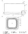
本発明の実施例1に係る半導体装置について、図1乃至図7を用いて説明する。図1は半導体装置を示す図で、図1(a)はその平面図、図1(b)は要部を示す拡大図、図2は半導体装置の等価回路を示す図、図3は半導体装置を示す図で、図3(a)は図1のA−A線に沿って切断し矢印方向に眺めた断面図、図3(b)は要部を示す拡大図、図4は半導体装置の効果を比較例と対比して示す図で、図4(a)が本実施例を示す図、図4(b)が比較例を示す図、図5乃至図7は半導体装置の製造工程を順に示す断面図である。 A semiconductor device according to
本実施例はトレンチゲートを有する絶縁ゲート電界効果トランジスタ(以後、単にMOSトランジスタという)と、両極性の静電放電からMOSトランジスタのゲート破壊を防止する保護ダイオードとを有する半導体装置の例である。 This embodiment is an example of a semiconductor device having an insulated gate field effect transistor (hereinafter simply referred to as a MOS transistor) having a trench gate and a protection diode for preventing gate breakdown of the MOS transistor from bipolar electrostatic discharge.
図1に示すように、本実施例の半導体装置10は、半導体基板の第1領域11に形成されたMOSトランジスタ12と、第1領域11に隣接した第2領域13に形成され、MOSトランジスタ12のゲート絶縁膜より厚く、且つ高濃度に不純物、例えば砒素を含有する図示されないシリコン酸化膜(第1シリコン酸化膜)と、シリコン酸化膜(第1シリコン酸化膜)上に形成されたポリシリコン層内に複数のPN接合を有するとともに、MOSトランジスタ12のゲートとソースとの間に接続され、MOSトランジスタ12のゲート破壊を防止する保護ダイオード14と、を具備している。 As shown in FIG. 1, the
第1領域11は、例えば角部が切り欠かれた矩形状の領域であり、第2領域13は角部の切り欠かれた領域である。
MOSトランジスタ12は、例えばストライプ状のトレンチゲート(図示せず)を有する縦型PチャネルMOSトランジスタである。The
The
保護ダイオード14は、例えばP+層15a、15c、15eとN−層15b、15dとが交互にリング状に接合した平面形状を有するポリシリコンダイオードである。
P+層15aをN−層15bが囲繞し、N−層15bをP+層15cが囲繞し、P+層15cをN−層15dが囲繞し、N−層15dをP+層15eが囲繞している。
周知のように、リング状のPN接合を有する保護ダイオード14は、PN接合のエッジ部を有しないので、エッジでの耐圧などの特性劣化が生じないという利点を有している。The
The P+ layer 15a N- layer 15b is surrounded, N- layer 15b surrounding theP +
As is well known, the
図2に示すように、MOSトランジスタ12は、ゲートがゲート配線20を介して外部入力端子21に接続され、ソースに電源Vddが供給され、ドレインが基準電位GNDに接続される。 As shown in FIG. 2, the
保護ダイオード14は、P+/N−/P+/N−/P+構造であり、等価的に4個のツェナーダイオードが交互に逆極性に直列接続(バック・ツー・バック接続)された双方向の保護ダイオードである。保護ダイオード14の一方がMOSトランジスタ12のゲートに接続され他方がソースに接続されている。The
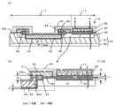
図3(a)に示すように、半導体装置10は、P+シリコン基板30と、P+シリコン基板30上に形成されたP−半導体層31とを有する半導体基板32と、半導体基板32のP−半導体層31に形成されたNベース層33とを具備し、半導体基板32の第1領域11にMOSトランジスタ12が形成され、半導体基板32の第2領域13に保護ダイオード14が形成されている。
ここで、保護ダイオード14は、リング状のP+/N−/P+/N−/P+構造の左半分のみを示している。As shown in FIG. 3 (a), the
Here, the
半導体基板32の第1領域11には、Nベース層33を貫通しP−半導体層31に達する図示されないトレンチの内壁にゲート絶縁膜(ゲート酸化膜)34が形成され、トレンチにゲート電極35が埋め込まれている。
Nベース層33の上部に、ゲート電極35をゲート長方向に挟むようにソース36が形成され、ソース36をゲート長方向に挟むようにソースコンタクト(メタル)37が形成されている。In the
A
P−半導体層31はキャリアのドリフト層となり、P+シリコン基板30はドレインとなる。
第1領域11の第2領域13側のNベース層33上には、ゲート絶縁膜34と同じ絶縁膜38が形成され、絶縁膜38上に一端がゲート電極35に接続され、他端が外部入力端子21に接続されるゲート配線20が形成されている。The P− semiconductor layer 31 becomes a carrier drift layer, and the P+ silicon substrate 30 becomes a drain.
The same insulating
図3(b)に示すように、半導体基板32の第2領域13には、ゲート絶縁膜34より厚く、且つ高濃度に砒素(As)を含有するシリコン酸化膜(第1シリコン酸化膜)40が形成されている。
シリコン酸化膜40上に、P+層15a、15c、15eとN−層15b、15dとが交互にリング状に接合して形成されている。As shown in FIG. 3B, the
On the
ゲート絶縁膜34の厚さt1は、例えば30nm程度であり、砒素を含有するシリコン酸化膜40の厚さt2はゲート絶縁膜34の厚さの3倍以上、例えば100nm程度に形成されている。
厚いシリコン酸化膜40は、周知のように、高濃度に砒素を含有するシリコンの増速酸化を利用して形成されている。増速酸化によれば、砒素の含有量、熱酸化条件に応じて、Asを含有しないシリコンに比べて2倍から10倍程度厚い熱酸化膜を得ることが容易である。The thickness t1 of the
As is well known, the thick
ゲート配線20および保護ダイオード14の周りには、それぞれシリコン酸化膜41、42が形成されている。
また、Nベース層33とソースコンタクト37との界面には、アバランシェ破壊を防止するために、キャリア濃度の高いN+型半導体層43が形成されている。
ゲート電極35上に保護膜44、ゲート配線20および保護ダイオード14上に保護膜45、46が形成されている。
Further, an N+
A
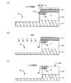
図4は半導体装置10の効果を比較例と対比して示す図で、図4(a)が本実施例を示す図、図4(b)が比較例を示す図である。ここで、比較例とは、保護ダイオード14がゲート絶縁膜34と等しい厚さのシリコン酸化膜上に形成されている半導体装置のことである。始めに、比較例について説明する。 4A and 4B are diagrams showing the effects of the
図4(b)に示すように、比較例ではシリコン酸化50がゲート絶縁膜34と同程度に薄いので、シリコン酸化膜50をゲート絶縁膜とし、Nベース層33をゲートとし、P+層15e、15c、15aをソース・ドレインとし、N−層15d、15bをベース層とするP型の寄生MOSトランジスタ51、52の直列回路が形成される。As shown in FIG. 4B, in the comparative example, since the
P+層15aが接続されたゲート電極35が順バイアスされ、P+層15eが接続されたソース36が逆バイアスされると、即ちゲート電極35が正電位、ソース36が接地電位GNDになるときに、ゲートとなるNベース層33の電位はソースコンタクト37、N+型半導体層43を介してソース36の電位とつながっているので、N−層15d、15bの底部の導電型がN型からP型に反転し、2つのP型の寄生MOSトランジスタ51、52がオンされる。
これにより、保護ダイオード14のP+層15aとP+層15e間にリーク電流ILが流れるので、保護ダイオード14の機能が損なわれ、信頼性に支障をきたす。When the
As a result, the leakage current IL flows between the P+ layer 15a and the P+ layer 15e of the
一方、図4(a)に示すように、本実施例では、シリコン酸化膜40がゲート絶縁膜34より3倍以上厚いので、保護ダイオード14は下地のNベース層33と完全に絶縁され、N−層15d、15bの底部の導電型がN型からP型に反転することは無く、保護ダイオード14の機能を維持し、高い信頼性を得ることが可能である。On the other hand, as shown in FIG. 4A, in this embodiment, since the
次に、半導体装置10の製造方法について説明する。図5乃至図7は半導体装置10の製造工程を順に示す断面図である。 Next, a method for manufacturing the
図5(a)に示すように、P+シリコン基板30と、P+シリコン基板30上にエピタキシャル成長により形成されたP−半導体層31とを有する半導体基板32に、例えば熱酸化法により厚さ200nm程度のシリコン酸化膜60を形成する。
次に、シリコン酸化膜60上にNベース層33に対応する開口を有するレジスト膜61を形成し、レジスト膜61をマスクとして、半導体基板32のP−半導体層31にシリコン酸化膜60を通して燐(P)をイオン注入し、Pイオン注入層62を形成する。As shown in FIG. 5A, a
Next, a resist
次に、図5(b)に示すように、レジスト膜61を除去した後、熱処理を施し、イオン注入したPを活性化し、N型半導体層63を形成する。
次に、シリコン酸化膜60上に第2領域13に対応する開口を有するレジスト膜64を形成し、レジスト膜64をマスクとして、第2領域13にシリコン酸化膜60を通して選択的にAsを高濃度(ドーズ量〜1E15atoms/cm2)にイオン注入し、Asイオン注入層(第1イオン注入層)65を形成する。Next, as shown in FIG. 5B, after removing the resist
Next, a resist
次に、図5(c)に示すように、レジスト膜64を除去した後、シリコン酸化膜60上にトレンチに対応する開口を有するマスク材66、例えばシリコン窒化膜を形成し、マスク材66を用いて、異方性エッチングにより第1領域11のP−半導体層31に所定の深さのトレンチ67を形成する。
この段階においては、半導体基板32の表面は平坦性が保たれているので、フォトリソグラフィ法により微細なトレンチパターンを形成することが可能である。Next, as shown in FIG. 5C, after removing the resist
At this stage, since the surface of the
次に、図6(a)に示すように、マスク材66を除去し、シリコン酸化膜60を除去し、半導体基板32の表面を露出させる。
次に、図6(b)に示すように、例えば温度1000℃、ドライ雰囲気で、第1領域11および第2領域13に熱処理を施す。Next, as shown in FIG. 6A, the
Next, as shown in FIG. 6B, heat treatment is performed on the
これにより、第1領域11および第2領域13のN型半導体層63中のPが熱拡散して、N型ベース層33が形成される。 Thereby, P in the N-
更に、第1領域11が熱酸化され、第1領域11のトレンチ67の内面に厚さ30nm程度のゲート絶縁膜34が形成され、Nベース層33の表面にゲート絶縁膜34と同じ厚さの絶縁膜38が形成される。
一方、高濃度にAsを含有する第2領域13は増速酸化され、第2領域13にゲート絶縁膜34より厚く、且つ高濃度にAsを含有する厚さ100nm程度のシリコン膜40が形成される。Further, the
On the other hand, the
次に、図6(c)に示すように、第1領域11および第2領域13の全面に、トレンチ67を埋め込むように、例えばCVD法により厚さ200nm程度のアンドープのポリシリコン層68を形成する。 Next, as shown in FIG. 6C, an
次に、図7(a)に示すように、ポリシリコン層68の全面にPをイオン注入(ドーズ量〜1E14atoms/cm2)し、ポリシリコン層68の導電型をN−型にする。
次に、図7(b)に示すように、第2領域13のポリシリコン層68上に2重リング状にレジスト膜69を形成し、レジスト膜69をマスクとして第1領域11および第2領域13のポリシリコン層68に硼素(B)をイオン注入(ドーズ量〜1E15atoms/cm2)し、ポリシリコン層68の導電型をN−型からP+型へ反転させ、第2領域13のポリシリコン層68内に複数のPN接合を形成する。Next, as shown in FIG. 7A, P is ion-implanted (dose amount˜1E14 atoms / cm2 ) into the entire surface of the
Next, as shown in FIG. 7B, a resist
次に、図7(c)に示すように、異方性エッチングにより、ポリシリコン層68を選択的に除去することにより、第1領域11にゲート電極35およびゲート電極を外部に電気的に接続するゲート配線20を形成し、同時に第2領域13にP+層とN−層が交互にリング状に接合する平面形状を有する保護ダイオード14を形成する。Next, as shown in FIG. 7C, the
次に、ゲート電極35を挟むようにソース36、ソースコンタクト37を形成し、P+シリコン基板30の裏面にドレイン電極(図示せず)を形成して、半導体装置10が得られる。Next, a
以上説明したように、本実施例では、第2領域13にAsを選択的にイオン注入し、高濃度にAsを含有するシリコンの増速酸化作用により、ゲート絶縁膜34より厚く、且つ高濃度にAsを含有するシリコン酸化膜40を形成し、シリコン酸化膜40上に保護ダイオード14を形成している。 As described above, in this embodiment, As is selectively ion-implanted into the
その結果、MOSトランジスタの性能向上を目的に、MOSトランジスタの微細化に応じて、ゲート絶縁膜を、例えば30nm以下に薄くしても、シリコン酸化膜40の厚さを100nm以上に維持することができる。 As a result, for the purpose of improving the performance of the MOS transistor, the thickness of the
これにより、ゲート電極35が順バイアスされ、ソース36が逆バイアスされたときに、寄生MOSトランジスタ51、52がオンし、保護ダイオード14の機能が損なわれることが防止することができる。
従って、高い信頼性を有し、微細化に好適な構造の保護ダイオードを備えた半導体装置およびその製造方法が得られる。Thereby, when the
Therefore, it is possible to obtain a semiconductor device including a protection diode having a high reliability and a structure suitable for miniaturization, and a manufacturing method thereof.
また、シリコン酸化膜40上に保護ダイオード14を形成する前に、トレンチ67を形成しているので、保護ダイオード14による半導体基板32の平坦性低下の影響を受けることなく微細なトレンチを容易に形成することができる。
更に、保護ダイオード14と同時にゲート配線20が形成できるので、製造工程を削減することができる。In addition, since the
Furthermore, since the
また、厚いシリコン酸化膜40の形成に高温長時間の熱酸化が不要なので、半導体基板32側から染み出した不純物が、MOSトランジスタ12のドレイン・ソース間の耐圧を低下させるなどの半導体装置の特性に支障をきたす恐れがない。 Further, since the thermal oxidation for a long time at high temperature is not required for forming the thick
ここでは、半導体装置10のMOSトランジスタ12がP−MOSトランジスタである場合について説明したが、N−MOSトランジスタであっても同様である。
MOSトランジスタ12がトレンチゲートを有する縦型MOSトランジスタである場合について説明したが、横型MOSトランジスタとすることもできる。ゲート電極は、トレンチ型だけでなく、プレーナ型とすることもできる。Although the case where the
Although the case where the
保護ダイオード14が4個のツェナーダイオードが互いに逆極性に接続されたダイオードである場合について説明したが、接続するツェナーダイオードの個数は特に限定されない。偶数個でも奇数個でも構わない。ツェナーダイオードの個数に応じて、ゲート電極34とソース36との間のゲート耐圧が増加する。 Although the case where the
保護ダイオード14がP+/N−/P+/N−/P+構造である場合について説明したが、N+/P−/N+/P−/N+構造することもできる。いずれの構造でも、同様の効果が得られる。Although the case where the
ポリシリコン層68がアンドープである場合について説明したが、N型不純物、例えばPを添加したドープドポリシリコンとすることもできる。その場合、Pをイオン注入してポリシリコン層68の導電型をN−型にする工程が削減できる利点がある。
第2領域13に選択的に注入する不純物がAsである場合について説明したが、PおよびBでも同様の効果を得ることができる。Although the case where the
Although the case where the impurity selectively implanted into the
本発明の実施例2に係る半導体装置について、図8乃至図12を用いて説明する。図8は半導体装置を示す図で、図8(a)はその平面図、図8(b)は要部を示す拡大図、図9は半導体装置を示す図で、図9(a)は図8のB−B線に沿って切断し矢印方向に眺めた断面図、図9(b)は要部を示す拡大図、図10乃至図12は半導体装置の製造工程の要部を順に示す断面図、図13は半導体装置の要部を比較例と対比して示す図で、図13(a)が本実施例の要部を示す図、図13(b)が比較例の要部を示す図である。 A semiconductor device according to Example 2 of the present invention will be described with reference to FIGS. 8A and 8B are diagrams showing the semiconductor device, FIG. 8A is a plan view thereof, FIG. 8B is an enlarged view showing the main part, FIG. 9 is a diagram showing the semiconductor device, and FIG. FIG. 9B is an enlarged view showing the main part, and FIGS. 10 to 12 are cross-sectional views showing the main part of the manufacturing process of the semiconductor device in order. FIGS. 13A and 13B are diagrams showing the main part of the semiconductor device in comparison with the comparative example. FIG. 13A shows the main part of this embodiment, and FIG. 13B shows the main part of the comparative example. FIG.
本実施例において、上記実施例1と同一の構成部分には同一符号を付してその部分の説明は省略し、異なる部分について説明する。
本実施例が実施例1と異なる点は、MOSトランジスタのゲート電極引き出し部をゲート絶縁膜より厚く、且つ高濃度にAsを含有するシリコン酸化膜上に形成したことにある。In the present embodiment, the same components as those in the first embodiment are denoted by the same reference numerals, description thereof will be omitted, and different portions will be described.
This embodiment is different from the first embodiment in that the gate electrode lead portion of the MOS transistor is formed on a silicon oxide film that is thicker than the gate insulating film and contains As at a high concentration.
即ち、図8に示すように本実施例の半導体装置80のMOSトランジスタ81は、ストライプ状のゲート電極82と、ゲート絶縁膜より厚く、且つ高濃度にAsを含有する第2シリコン酸化膜83と、第2シリコン酸化膜83を覆うように形成されたゲート配線84とを具備している。
ゲート電極82の端部82aとゲート配線84の側部84aとがオーバラップして接触し、ゲート電極引き出し部85を構成している。ゲート配線84は複数のゲート電極82を取り囲むように形成され、ゲート電極82の両方の端部がオーバラップしてゲート配線84に接触している。
具体的には、図9に示すように、ゲート電極82は、半導体基板32の第1領域11の主面32aに形成された図示されないトレンチ67内に、ゲート絶縁膜34を介してポリシリコン層68が埋め込まれて形成されている。That is, as shown in FIG. 8, the
The
Specifically, as shown in FIG. 9, the
第2シリコン酸化膜83は、半導体基板32の主面32aとトレンチ67の端部の側面とにより構成される角部86に形成されている。第2シリコン酸化膜83は、シリコン酸化膜40と同じく高濃度のAsを含有し、同じ厚さt2を有している。 The second
ゲート配線84は、第2シリコン酸化膜83を含んで角部86を覆うように形成されたポリシリコン層68を有し、ゲート電極82の端部82aの上面とゲート配線84の側部84aの下面とがオーバラップして接触している。 The
次に、半導体装置80の製造方法について説明する。図10および図11は半導体装置80の製造工程の要部を順に示す断面図である。
図10(a)に示すように、図5(b)に示す不純物をイオン注入する工程において、第1領域11を被覆するシリコン酸化膜60(図示せず)上に形成された開口を有するレジスト膜64(被覆材)をマスクとし、シリコン酸化膜60を通して選択的にAsを高濃度(ドーズ量〜1E15atoms/cm2)にイオン注入し、Asイオン注入層(第2イオン注入層)90を第2領域13のAsイオン注入層65と同時に形成する。Next, a method for manufacturing the
As shown in FIG. 10A, in the step of ion-implanting the impurity shown in FIG. 5B, a resist having an opening formed on a silicon oxide film 60 (not shown) covering the
次に、図10(b)に示すように、レジスト膜64を除去した後、図5(c)に示すトレンチを形成する工程において、トレンチ67に対応する開口を有するマスク材91、ここではアンドープのシリコン酸化膜の形成を、Asイオン注入層90の一部90a(端部から長さL1まで)がトレンチ67の端部の側面を構成するように行う。 Next, as shown in FIG. 10B, after removing the resist
次に、図10(c)に示すように、マスク材91を用いて、異方性エッチングにより第1領域11のP−半導体層31に至る所定の深さのトレンチ67を形成する。これにより、Asイオン注入層90の一部90aがトレンチ67の端部67aの側面を構成する。Next, as shown in FIG. 10C, a
次に、図11(a)に示すように、マスク材91をフッ化水素酸(HF)とフッ化アンモニウム(NH4F)を混合したバッファードフッ酸(BHF)を用いて部分的にエッチングし、マスク材91の厚さを目減りさせながら、マスク材91をトレンチ67の端部67aより長さL2だけ後退させる。Next, as shown in FIG. 11A, the
次に、図11(b)に示すように、マスク材91をマスクとして塩素系/フッ素系ガスを用いたCDE(Chemical Dry Etching)法により、トレンチ67の内壁を等方性エッチング、所謂エッチバックして、トレンチ67の内壁のダメージを除去し、ラフネスを改善する。
このとき、マスク材91の直下のトレンチ67の端部67aはシリコンのエッチングレートが遅くなるため、角部86が鋭角を有するようになる。Next, as shown in FIG. 11B, the inner wall of the
At this time, the
次に、図11(c)に示すように、図6(a)の工程において、マスク材91およびシリコン酸化膜60を除去し、半導体基板32の主面32aを露出させる。 Next, as shown in FIG. 11C, in the step of FIG. 6A, the
次に、図12(a)に示すように、図6(b)に示す半導体基板32に熱処理を施す工程において、高濃度にAsを含有するAsイオン注入層90は増速酸化されるので、角部86にゲート絶縁膜34より厚く、且つ高濃度にAsを含有する第2シリコン酸化膜83が、シリコン酸化膜40と同時に形成される。 Next, as shown in FIG. 12A, in the step of performing a heat treatment on the
次に、図12(b)に示すように、図6(c)に示すポリシリコン層68を形成する工程において、トレンチ67を埋め込み、第2シリコン酸化膜83を覆うようにポリシリコン層68を形成する。 Next, as shown in FIG. 12B, in the step of forming the
次に、図12(c)に示すように、図7(c)に示すポリシリコンを選択的に除去する工程において、ゲート電極としてトレンチ67内にゲート絶縁膜34を介してポリシリコン層68が埋め込まれたゲート電極82を形成し、ゲート電極82の端部82aの上面に側部84aの下面がオーバラップして接触したゲート配線84を形成する。これにより、上述したゲート電極引き出し部85が得られる。 Next, as shown in FIG. 12C, in the step of selectively removing the polysilicon shown in FIG. 7C, the
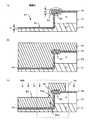
図13は半導体装置80の要部を比較例と対比して示す図で、図13(a)が本実施例の要部を示す図、図13(b)が比較例の要部を示す図である。ここで、比較例とは、Asイオン注入層90を形成しないで製造された半導体装置のことである。始めに、比較例について説明する。 FIG. 13 is a diagram showing the main part of the
比較例では図10(a)に示すAsイオン注入層90を形成しないで、図11(c)に示すトレンチ67を形成した後、半導体基板32に熱処理を施している。
その結果、図13(b)に示すように、鋭角を有する角部86において酸化に供されるシリコンの量が少ないため、形成されるシリコン酸化膜93の膜厚t3はゲート絶縁膜34の膜厚t1より薄くなる。
鋭角を有する角部86には機械的・熱的応力集中および電界集中が生じ易いことに加え、角部86のシリコン酸化膜93はゲート絶縁膜34より薄いので破壊耐量が低下する問題がある。In the comparative example, the As
As a result, as shown in FIG. 13B, since the amount of silicon subjected to oxidation is small at the
The
一方、図13(a)に示す本実施例では、上述したように角部86に高濃度にAsを含有するAsイオン注入層90を形成し、トレンチ67を形成した後、半導体基板32に熱処理を施している。
その結果、Asイオン注入層90が増速酸化されるので、鋭角を有する角部86において形成される第2シリコン酸化膜83の膜厚はゲート絶縁膜34の膜厚t1より厚いt2になる。
これにより、角部86に機械的・熱的応力集中および電界集中が生じても、角部86のシリコン酸化膜83はゲート絶縁膜34より厚いのでの破壊耐量を向上させることができる。On the other hand, in the present embodiment shown in FIG. 13A, as described above, the As ion-implanted
As a result, the As ion-implanted
Thereby, even if mechanical / thermal stress concentration and electric field concentration occur in the
以上説明したように、本実施例では、半導体基板32の主面32aとトレンチ67の端部67aの側面とにより構成される角部86にAsを選択的にイオン注入し、高濃度にAsを含有するシリコンの増速酸化作用により、ゲート絶縁膜34より厚く、且つ高濃度にAsを含有する第2シリコン酸化膜83を形成し、第2シリコン酸化膜83を含む角部86を覆うようにゲート配線84を形成している。 As described above, in the present embodiment, As is selectively ion-implanted into the
その結果、MOSトランジスタの性能向上を目的に、MOSトランジスタの微細化に応じて、ゲート絶縁膜34を、例えば30nm以下に薄くしても、第2シリコン酸化膜83の厚さを100nm以上に維持することができる。従って、角部86のシリコン酸化膜の破壊耐量を向上させることができる利点がある。 As a result, for the purpose of improving the performance of the MOS transistor, the thickness of the second
本発明は、以下の付記に記載されているような構成が考えられる。
(付記1) 複数の前記ゲート電極を有し、前記ゲート配線が複数の前記ゲート電極を取り囲み、前記ゲート電極の両方の端部が前記ゲート配線に接触している請求項2に記載の半導体装置。The present invention can be configured as described in the following supplementary notes.
(Supplementary note 1) The semiconductor device according to
10、80 半導体装置
11 第1領域
12、81 MOSトランジスタ
13 第2領域
14 保護ダイオード
15a、15c、15e P+層
15b、15d N−層
20、84 ゲート配線
21 外部入力端子
30 P+シリコン基板
31 P−半導体層
32 半導体基板
32a 主面
33 Nベース層
34 ゲート絶縁膜
35、82 ゲート電極
36 ソース
37 ソースコンタクト
38 絶縁膜
40、41、42、50、60、93 シリコン酸化膜
43 N+型半導体層
44、45、46 保護膜
51、52 寄生MOSトランジスタ
61、64、69 レジスト膜
62 Pイオン注入層
63 N型半導体層
65、90 Asイオン注入層
66、91 マスク材
67 トレンチ
68 ポリシリコン層
IL リーク電流
82a 端部
83 第2シリコン酸化膜
84a 側部
85 ゲート電極引き出し部
86 角部DESCRIPTION OF
Claims (5)
Translated fromJapanese前記第1領域に形成されたゲート絶縁膜と、
前記第1領域に隣接する第2領域に形成された酸化層と、
前記第2領域に形成され、前記ゲート絶縁膜及び前記酸化層よりも厚く、且つ不純物を含有する第1シリコン酸化層と、
前記第1シリコン酸化層上に形成されたポリシリコン層内に複数のPN接合を有するとともに、前記絶縁ゲート電界効果トランジスタのゲートとソースとの間に接続される保護ダイオードと、
を具備することを特徴とする半導体装置。An insulated gate field effect transistor formed in the first region of the semiconductor substrate;
A gateinsulating film formed in the first region;
An oxide layer formed in a second region adjacent to the first region;
A first silicon oxide layer formed in the second region, thicker than the gate insulating film and the oxide layer and containing impurities;
A protection diode having a plurality of PN junctions in a polysilicon layer formed on the first silicon oxidelayer and connected between a gate and a source of the insulated gate field effect transistor;
A semiconductor device comprising:
前記第1領域を被覆して、前記第2領域に対し選択的に、前記第1領域より高濃度に不純物をイオン注入して第1イオン注入層を形成する工程と、
前記第1領域及び前記第2領域を熱処理酸化することにより、前記第1領域にゲート絶縁膜を形成するとともに、前記第1イオン注入層を酸化して前記ゲート絶縁膜より厚い第1シリコン酸化層を形成する工程と、
前記ゲート絶縁膜および前記第1シリコン酸化層上にポリシリコン層を形成する工程と、
前記第2領域の前記ポリシリコン層内に複数のPN接合を形成する工程と、
異方性エッチングにより前記ポリシリコン層を選択的に除去し、前記第1領域にゲート電極を形成する工程と、
を具備することを特徴とする半導体装置の製造方法。A semiconductor device having an insulated gate field effect transistor in a first region of a semiconductor substrate, anda protection diode connected between a gate and a source of the insulated gate field effect transistor in a second region adjacent to the first region A manufacturing method of
And covering the first region, selectivelyagainst the secondregion, forming a first ion-implantation layer by implanting impurity at a high concentration than said first region,
A first silicon oxidelayerthicker than thegate insulating film is formed by forming a gate insulating film in the first region byoxidizing the first region and the second region by heat treatment and oxidizingthe first ion implantationlayer. Forming a step;
Forming a polysilicon layer onthegate insulating film andthe first silicon oxide layer ;
Forming a plurality of PN junctions in the polysilicon layer of the second region;
Selectively removing the polysilicon layer by anisotropic etchingand forming a gate electrode in the first region ;
A method for manufacturing a semiconductor device, comprising:
前記第1イオン注入層を形成する工程において、前記第1領域を被覆する被覆材に形成された開口を通して、前記第1領域において選択的に、前記第1領域より高濃度に前記不純物がイオン注入された第2イオン注入層を形成し、
前記トレンチを形成する工程において、前記第2イオン注入層の一部が端部の側面を構成するようにトレンチを形成し、
前記熱処理酸化を施す工程において、ゲート絶縁膜を前記トレンチの内側に形成し、前記第2イオン注入層を酸化して前記絶縁層より厚い第2シリコン酸化層を形成し、
前記ポリシリコン層を形成する工程において、前記トレンチを埋め込み、前記第2シリコン酸化層を覆うように前記ポリシリコン層を形成し、
前記ポリシリコン層を選択的に除去する工程において、前記ゲート電極として前記トレンチ内に前記ゲート絶縁膜を介して前記ポリシリコン層が埋め込まれたゲート電極を形成し、前記ゲート電極の端部に接触したゲート配線を形成することを特徴とする請求項4に記載の半導体装置の製造方法。And a step of forming a trench in the first region by following the anisotropic etching step of formingthe first ion implantation layerthe impurity is ion-implanted,
Inthe step of formingthe first ion implantation layer through an opening formed in the covering material that covers the first region, theOite selectively to said firstregion, said impurity concentration higher than said first region Forming a second ion-implanted ion-implanted layer;
In the step of forming the trench, the trench is formed such that a part of the second ion implantation layer constitutes a side surface of the end portion,
In the heat treatment oxidation step, agate insulating film is formed inside the trench, the second ion implantation layer is oxidized to form a second silicon oxidelayerthicker than theinsulating layer ,
In the step of forming the polysilicon layer, the polysilicon layer is formed so as to fill the trench and cover the second silicon oxidelayer ,
In the step of selectively removing the polysilicon layer, a gate electrode in which the polysilicon layer is embedded in the trench via the gate insulating film is formed as the gate electrode, and is in contact with an end portion of the gate electrode 5. The method of manufacturing a semiconductor device according to claim 4, wherein the gate wiring is formed.
Priority Applications (2)
| Application Number | Priority Date | Filing Date | Title |
|---|---|---|---|
| JP2009013512AJP5331497B2 (en) | 2008-11-27 | 2009-01-23 | Semiconductor device and manufacturing method thereof |
| US12/626,414US8183606B2 (en) | 2008-11-27 | 2009-11-25 | Semiconductor device and method of manufacturing the same |
Applications Claiming Priority (3)
| Application Number | Priority Date | Filing Date | Title |
|---|---|---|---|
| JP2008302103 | 2008-11-27 | ||
| JP2008302103 | 2008-11-27 | ||
| JP2009013512AJP5331497B2 (en) | 2008-11-27 | 2009-01-23 | Semiconductor device and manufacturing method thereof |
Publications (2)
| Publication Number | Publication Date |
|---|---|
| JP2010153762A JP2010153762A (en) | 2010-07-08 |
| JP5331497B2true JP5331497B2 (en) | 2013-10-30 |
Family
ID=42195437
Family Applications (1)
| Application Number | Title | Priority Date | Filing Date |
|---|---|---|---|
| JP2009013512AActiveJP5331497B2 (en) | 2008-11-27 | 2009-01-23 | Semiconductor device and manufacturing method thereof |
Country Status (2)
| Country | Link |
|---|---|
| US (1) | US8183606B2 (en) |
| JP (1) | JP5331497B2 (en) |
Families Citing this family (6)
| Publication number | Priority date | Publication date | Assignee | Title |
|---|---|---|---|---|
| KR101194973B1 (en)* | 2010-04-27 | 2012-10-25 | 에스케이하이닉스 주식회사 | Transistor of semiconductor device and method of forming the same |
| JP5788678B2 (en)* | 2011-01-05 | 2015-10-07 | ローム株式会社 | Semiconductor device and manufacturing method thereof |
| WO2014024595A1 (en)* | 2012-08-09 | 2014-02-13 | 富士電機株式会社 | Semiconductor device and method for producing same |
| ITMI20121599A1 (en)* | 2012-09-25 | 2014-03-26 | St Microelectronics Srl | ELECTRONIC DEVICE INCLUDING A VTMOS TRANSISTOR AND AN INTEGRATED THERMAL DIODE |
| US10090294B2 (en) | 2016-03-04 | 2018-10-02 | Rohm Co., Ltd. | Semiconductor device |
| JP6430424B2 (en)* | 2016-03-08 | 2018-11-28 | 株式会社東芝 | Semiconductor device |
Family Cites Families (30)
| Publication number | Priority date | Publication date | Assignee | Title |
|---|---|---|---|---|
| JPS62165951A (en)* | 1986-01-17 | 1987-07-22 | Sanyo Electric Co Ltd | Manufacture of semiconductor device |
| US5644157A (en)* | 1992-12-25 | 1997-07-01 | Nippondenso Co., Ltd. | High withstand voltage type semiconductor device having an isolation region |
| US20020036326A1 (en)* | 1994-08-11 | 2002-03-28 | Harris Corporation | Analog-to-digital converter and method of fabrication |
| US6049108A (en)* | 1995-06-02 | 2000-04-11 | Siliconix Incorporated | Trench-gated MOSFET with bidirectional voltage clamping |
| JPH1187336A (en)* | 1997-09-12 | 1999-03-30 | New Japan Radio Co Ltd | Manufacture of semiconductor device |
| TW501230B (en)* | 1997-10-04 | 2002-09-01 | United Microelectronics Corp | Manufacture method shallow trench isolation |
| JPH11330458A (en)* | 1998-05-08 | 1999-11-30 | Toshiba Corp | Semiconductor device and manufacturing method thereof |
| US6413822B2 (en)* | 1999-04-22 | 2002-07-02 | Advanced Analogic Technologies, Inc. | Super-self-aligned fabrication process of trench-gate DMOS with overlying device layer |
| US6365932B1 (en)* | 1999-08-20 | 2002-04-02 | Denso Corporation | Power MOS transistor |
| JP4846106B2 (en)* | 2001-02-16 | 2011-12-28 | 三菱電機株式会社 | Field effect semiconductor device and method for manufacturing the same |
| US6635537B2 (en)* | 2001-04-06 | 2003-10-21 | United Microelectronics Corp. | Method of fabricating gate oxide |
| JP3551947B2 (en) | 2001-08-29 | 2004-08-11 | サンケン電気株式会社 | Semiconductor device and manufacturing method thereof |
| JP4740523B2 (en) | 2003-01-27 | 2011-08-03 | ルネサスエレクトロニクス株式会社 | Insulated gate semiconductor device |
| JP4136778B2 (en)* | 2003-05-07 | 2008-08-20 | 富士電機デバイステクノロジー株式会社 | Insulated gate bipolar transistor |
| US6943396B2 (en)* | 2003-06-17 | 2005-09-13 | Infineon Technologies Ag | Electro-static discharge protection circuit and method for making the same |
| JP4955222B2 (en)* | 2005-05-20 | 2012-06-20 | ルネサスエレクトロニクス株式会社 | Manufacturing method of semiconductor device |
| JP2007189192A (en)* | 2005-12-15 | 2007-07-26 | Toshiba Corp | Semiconductor device |
| US20070176239A1 (en)* | 2006-01-31 | 2007-08-02 | M-Mos Semiconductor Sdn. Bhd. | Trenched MOSFETS with improved ESD protection capability |
| JP2007220814A (en)* | 2006-02-15 | 2007-08-30 | Sanyo Electric Co Ltd | Semiconductor device |
| US7633119B2 (en)* | 2006-02-17 | 2009-12-15 | Alpha & Omega Semiconductor, Ltd | Shielded gate trench (SGT) MOSFET devices and manufacturing processes |
| DE102007063728B4 (en)* | 2006-03-07 | 2018-12-13 | Infineon Technologies Ag | Semiconductor device arrangement with a trench transistor |
| JP5044950B2 (en)* | 2006-03-14 | 2012-10-10 | 株式会社デンソー | Semiconductor device |
| JP5048273B2 (en)* | 2006-05-10 | 2012-10-17 | オンセミコンダクター・トレーディング・リミテッド | Insulated gate semiconductor device |
| JP5222466B2 (en)* | 2006-08-09 | 2013-06-26 | ルネサスエレクトロニクス株式会社 | Semiconductor device and manufacturing method thereof |
| JP4286877B2 (en)* | 2007-03-13 | 2009-07-01 | Okiセミコンダクタ株式会社 | Silicon carbide semiconductor device and manufacturing method thereof |
| US7511357B2 (en)* | 2007-04-20 | 2009-03-31 | Force-Mos Technology Corporation | Trenched MOSFETs with improved gate-drain (GD) clamp diodes |
| US7585705B2 (en)* | 2007-11-29 | 2009-09-08 | Alpha & Omega Semiconductor, Inc. | Method for preventing gate oxide damage of a trench MOSFET during wafer processing while adding an ESD protection module atop |
| US7825431B2 (en)* | 2007-12-31 | 2010-11-02 | Alpha & Omega Semicondictor, Ltd. | Reduced mask configuration for power MOSFETs with electrostatic discharge (ESD) circuit protection |
| US7897997B2 (en)* | 2008-02-23 | 2011-03-01 | Force Mos Technology Co., Ltd. | Trench IGBT with trench gates underneath contact areas of protection diodes |
| US8022470B2 (en)* | 2008-09-04 | 2011-09-20 | Infineon Technologies Austria Ag | Semiconductor device with a trench gate structure and method for the production thereof |
- 2009
- 2009-01-23JPJP2009013512Apatent/JP5331497B2/enactiveActive
- 2009-11-25USUS12/626,414patent/US8183606B2/enactiveActive
Also Published As
| Publication number | Publication date |
|---|---|
| JP2010153762A (en) | 2010-07-08 |
| US20100127330A1 (en) | 2010-05-27 |
| US8183606B2 (en) | 2012-05-22 |
Similar Documents
| Publication | Publication Date | Title |
|---|---|---|
| US5872037A (en) | Method for manufacturing a vertical mosfet including a back gate electrode | |
| US6518623B1 (en) | Semiconductor device having a buried-channel MOS structure | |
| JP5172654B2 (en) | Semiconductor device | |
| JP5703790B2 (en) | Semiconductor device and manufacturing method thereof | |
| JP2008078654A (en) | Semiconductor device and manufacturing method thereof | |
| KR101355282B1 (en) | Semiconductor device and method of manufacturing the same | |
| JP5331497B2 (en) | Semiconductor device and manufacturing method thereof | |
| CN102315219A (en) | Semiconductor device and manufacturing approach thereof | |
| JP2800702B2 (en) | Semiconductor device | |
| JP2014203851A (en) | Semiconductor device and manufacturing method of the same | |
| TWI725356B (en) | Semiconductor device and method for manufacturing the same | |
| JP5360735B2 (en) | Semiconductor device | |
| JP4783050B2 (en) | Semiconductor device and manufacturing method thereof | |
| JP2010177292A (en) | Semiconductor device and method for manufacturing the same | |
| JP2009158621A (en) | Semiconductor device | |
| JP4579512B2 (en) | Semiconductor device and manufacturing method thereof | |
| JP4961686B2 (en) | Semiconductor device | |
| CN113644135B (en) | Field effect transistor and method of manufacturing the same | |
| JP2006013450A (en) | Semiconductor device and manufacturing method thereof | |
| JP6707917B2 (en) | Semiconductor device and manufacturing method thereof | |
| JP2010212588A (en) | Semiconductor element, semiconductor device and method for manufacturing the semiconductor element | |
| JP6641958B2 (en) | Semiconductor device and manufacturing method thereof | |
| JP4950648B2 (en) | Semiconductor device and manufacturing method thereof | |
| JP5071652B2 (en) | Semiconductor device | |
| JPH03129777A (en) | Semiconductor device provided with fet and manufacture thereof |
Legal Events
| Date | Code | Title | Description |
|---|---|---|---|
| A621 | Written request for application examination | Free format text:JAPANESE INTERMEDIATE CODE: A621 Effective date:20110223 | |
| RD02 | Notification of acceptance of power of attorney | Free format text:JAPANESE INTERMEDIATE CODE: A7422 Effective date:20111125 | |
| RD04 | Notification of resignation of power of attorney | Free format text:JAPANESE INTERMEDIATE CODE: A7424 Effective date:20111205 | |
| A977 | Report on retrieval | Free format text:JAPANESE INTERMEDIATE CODE: A971007 Effective date:20130123 | |
| A131 | Notification of reasons for refusal | Free format text:JAPANESE INTERMEDIATE CODE: A131 Effective date:20130125 | |
| A521 | Request for written amendment filed | Free format text:JAPANESE INTERMEDIATE CODE: A523 Effective date:20130319 | |
| A131 | Notification of reasons for refusal | Free format text:JAPANESE INTERMEDIATE CODE: A131 Effective date:20130405 | |
| A521 | Request for written amendment filed | Free format text:JAPANESE INTERMEDIATE CODE: A523 Effective date:20130426 | |
| TRDD | Decision of grant or rejection written | ||
| A01 | Written decision to grant a patent or to grant a registration (utility model) | Free format text:JAPANESE INTERMEDIATE CODE: A01 Effective date:20130705 | |
| A61 | First payment of annual fees (during grant procedure) | Free format text:JAPANESE INTERMEDIATE CODE: A61 Effective date:20130729 | |
| R151 | Written notification of patent or utility model registration | Ref document number:5331497 Country of ref document:JP Free format text:JAPANESE INTERMEDIATE CODE: R151 |