Movatterモバイル変換


[0]ホーム

URL:


JP5330944B2 - Light emitting device - Google Patents

Light emitting device
Download PDF

Info

Publication number
JP5330944B2
JP5330944B2JP2009217335AJP2009217335AJP5330944B2JP 5330944 B2JP5330944 B2JP 5330944B2JP 2009217335 AJP2009217335 AJP 2009217335AJP 2009217335 AJP2009217335 AJP 2009217335AJP 5330944 B2JP5330944 B2JP 5330944B2
Authority
JP
Japan
Prior art keywords
light
columnar body
emitting device
light emitting
light source
Prior art date
Legal status (The legal status is an assumption and is not a legal conclusion. Google has not performed a legal analysis and makes no representation as to the accuracy of the status listed.)
Active
Application number
JP2009217335A
Other languages
Japanese (ja)
Other versions
JP2011066307A (en
Inventor
良二 横谷
Current Assignee (The listed assignees may be inaccurate. Google has not performed a legal analysis and makes no representation or warranty as to the accuracy of the list.)
Panasonic Corp
Panasonic Holdings Corp
Original Assignee
Panasonic Corp
Matsushita Electric Industrial Co Ltd
Priority date (The priority date is an assumption and is not a legal conclusion. Google has not performed a legal analysis and makes no representation as to the accuracy of the date listed.)
Filing date
Publication date
Application filed by Panasonic Corp, Matsushita Electric Industrial Co LtdfiledCriticalPanasonic Corp
Priority to JP2009217335ApriorityCriticalpatent/JP5330944B2/en
Priority to CN2010102877861Aprioritypatent/CN102022643A/en
Publication of JP2011066307ApublicationCriticalpatent/JP2011066307A/en
Application grantedgrantedCritical
Publication of JP5330944B2publicationCriticalpatent/JP5330944B2/en
Activelegal-statusCriticalCurrent
Anticipated expirationlegal-statusCritical

Links

Images

Classifications

Landscapes

Abstract

The invention discloses a light producing device which can ensure control of light distribution by means of optical elements and reduce unevenness of illuminance of light on an irradiated surface. The light producing device (10) herein comprises a light source part (9) which contains a plurality of LED chips (optical elements) (1), at least one portion which is internally provided with the said light source part (9), an optical element (2) which enables a reflection surface which reflects light from the light source part (9) to become a rotary surface, wherein the light source part (9) inside the optical element (2) comprises a polygonal column body (3) which runs along a rotary shaft (A) on the rotary surface in length direction and a light conversion component (4) which encloses the column body (3) for absorbing at least part of the light emitted by LED chips (1) which are disposed on side wall (3a) of the column body (3) and subsequently change the wavelength of the side light absorbed.

Description

Translated fromJapanese

本発明は、複数個の発光素子を用いた発光装置に関するものである。  The present invention relates to a light emitting device using a plurality of light emitting elements.

近年、半導体を用いた発光素子と、該発光素子からの光の一部を吸収して波長変換した光を発する蛍光体との組み合わせにより、白色光などの混色光を発光可能な発光装置が開発されている。このような発光装置は、より光出力特性の優れた発光素子が急激な勢いで開発されてきていることから、一部には照明用途までにも利用され始めている。  In recent years, a light-emitting device capable of emitting mixed-color light such as white light has been developed by combining a light-emitting element using a semiconductor and a phosphor that emits light whose wavelength is converted by absorbing part of the light from the light-emitting element. Has been. Such light-emitting devices have begun to be used partially for lighting applications because light-emitting elements with more excellent light output characteristics have been developed at a rapid pace.

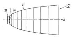
この種の発光装置として、図16には、発光素子たるLEDチップ1を円板状の放熱板31上に配置した光源部と、該光源部を円錐筒状の回転曲面反射鏡における開口部2aを塞ぐように配置し、内面が前記光源部からの光を外部に反射する前記回転曲面反射鏡の回転面とする光学素子2と、を備えた発光装置10’が知られている(たとえば、特許文献1を参照。)。なお、光学素子2の前記回転面における回転軸Aが、発光装置10’の光軸となる。また、LEDチップ1は、1個でもよいし複数個でもよく、蛍光体付きのLEDであってもよいことが開示されている。  As a light-emitting device of this type, FIG. 16 shows a light source part in which anLED chip 1 as a light-emitting element is arranged on a disk-shaped heat sink 31 and an opening 2a in a conical cylindrical rotary curved reflector. And alight emitting device 10 ′ including anoptical element 2 whose inner surface is a rotating surface of the rotating curved reflecting mirror that reflects light from the light source unit to the outside (for example, (See Patent Document 1). The rotation axis A on the rotation surface of theoptical element 2 is the optical axis of the light emitting device 10 '. Further, it is disclosed that theLED chip 1 may be one or plural, and may be an LED with a phosphor.

これにより、発光装置10’は、光学素子2がLEDチップ1からの光を反射して、所望の配光特性を得ることができる、とされている。  Thereby, in thelight emitting device 10 ′, theoptical element 2 reflects the light from theLED chip 1, and a desired light distribution characteristic can be obtained.

しかしながら、LEDチップ1自身から放出される光の指向性は、強い。そのため、図16に示す発光装置10’では、LEDチップ1を面光源として光学素子2の開口部2aに配置させて前記光源部から略均一な輝度分布で発光させたとしても、光学素子2に入射することなく発光装置10’の回転軸A方向へ放射される直接光が多くを占め、光学素子2による配光制御が困難となる。  However, the directivity of light emitted from theLED chip 1 itself is strong. Therefore, in thelight emitting device 10 ′ shown in FIG. 16, even if theLED chip 1 is arranged as a surface light source in the opening 2a of theoptical element 2 and light is emitted from the light source part with a substantially uniform luminance distribution, Direct light radiated in the direction of the rotation axis A of thelight emitting device 10 ′ without entering the light occupies a large amount, and light distribution control by theoptical element 2 becomes difficult.

発光装置10’からの照射光により形成される照射パターンには、主として、被照射面の略中央に光学素子2で制御された光が多くなる高照度領域と、該高照射領域の外側にLEDチップ1からの直接光で形成されるリング状の低照度領域とで形成される照度むらが生ずることになる。  The irradiation pattern formed by the irradiation light from thelight emitting device 10 ′ mainly includes a high illuminance region where light controlled by theoptical element 2 is increased in the approximate center of the irradiated surface, and an LED outside the high irradiation region. Irradiance unevenness formed by the ring-shaped low illuminance region formed by direct light from thechip 1 occurs.

また、図17に示す、複数個の発光素子たるLEDチップ1を備えた光源部9’と、光源部9’を内部に配し、内面が光源部9’からの光を外部に反射させる反射板からなる光学素子2とを備えた発光装置10’であって、光源部9’が、光学素子2の光軸Xに沿って長手方向が配される多角形状の柱状体3と、該柱状体3の側面3aに複数個のLEDチップ1を実装した長尺の実装基板5とを有する発光装置10’も提案されている(たとえば、特許文献2、特許文献3を参照。)
なお、図17に示す発光装置10’では、柱状体3の先端部に、発光装置10’の中心が暗くなるのを抑制しつつ放熱性を確保する別体の反射部材8’を一体的に配置してある。
In addition, alight source unit 9 ′ having a plurality of light emittingelements LED chip 1 shown in FIG. 17 and alight source unit 9 ′ are arranged inside, and the inner surface reflects light from thelight source unit 9 ′ to the outside. A light-emitting device 10 ′ having a plate-shapedoptical element 2, wherein alight source unit 9 ′ is a polygonalcolumnar body 3 whose longitudinal direction is arranged along the optical axis X of theoptical element 2, and the columnar shape Alight emitting device 10 ′ having along mounting substrate 5 in which a plurality ofLED chips 1 are mounted on aside surface 3a of thebody 3 has also been proposed (see, for example,Patent Document 2 and Patent Document 3).
In thelight emitting device 10 ′ shown in FIG. 17, a separate reflectingmember 8 ′ that secures heat dissipation while integrally suppressing the dark center of thelight emitting device 10 ′ is integrally formed at the tip of thecolumnar body 3. It is arranged.

図17の発光装置10’は、複数個のLEDチップ1を列状に実装した実装基板5を多角柱状をした柱状体3の側面3aに搭載した光源部9’とすることにより、光学素子2の配光制御性を高め、上述の照射パターンが、主として、被照射面の略中央の高照度領域と、該高照射領域の外側に形成される低照度領域とで形成される照度むらを抑制することが可能となる。  In thelight emitting device 10 ′ of FIG. 17, amounting substrate 5 on which a plurality ofLED chips 1 are mounted in a row is used as alight source unit 9 ′ mounted on aside surface 3a of acolumnar body 3 having a polygonal columnar shape, whereby anoptical element 2 is obtained. The above-mentioned irradiation pattern mainly suppresses illuminance unevenness formed by the high illuminance region at the approximate center of the irradiated surface and the low illuminance region formed outside the high irradiation region. It becomes possible to do.

特開2007−235079号公報JP 2007-235079 A特開2006−310502号公報JP 2006-310502 A特開2004−342574号公報JP 2004-342574 A

しかしながら、発光装置10’は、コスト低減や低消費電力を目的として、LEDチップ1の数を減らす傾向にあり、LEDチップ1を柱状体3の側面3a上に隙間なく立体的に配置させるのは難しい。そのため、図17の発光装置10’では、実装基板5に実装されたLEDチップ1間だけでなく、隣接する実装基板5に搭載されたLEDチップ1との間も非発光部となり、光源部9’自体に輝度むらが生ずることになる。これは、LEDチップ1を上述の蛍光体付きのLEDに単に置き換えても同様に生ずる。このため、発光装置10’は、光学素子2で光源部9’からの光を制御するように設計しても、発光装置10’からの照射光により形成される照射パターンに光源部9’の輝度むらが反映される。特に、発光装置10’は、光学素子2が光源部9’からの光を広角よりも狭角に絞る設計構造の場合、発光装置10’から照射された光に光源部9’の輝度むらに起因する照度むらが顕著に生ずる傾向にある。  However, thelight emitting device 10 ′ tends to reduce the number ofLED chips 1 for the purpose of cost reduction and low power consumption, and theLED chips 1 are arranged three-dimensionally on theside surface 3 a of thecolumnar body 3 without a gap. difficult. Therefore, in thelight emitting device 10 ′ of FIG. 17, not only between theLED chips 1 mounted on themounting substrate 5 but also between theLED chips 1 mounted on theadjacent mounting substrate 5 becomes a non-light emitting portion, and the light source unit 9 'It will cause uneven brightness. This similarly occurs even when theLED chip 1 is simply replaced with the LED with the phosphor described above. For this reason, even if thelight emitting device 10 ′ is designed so that the light from thelight source unit 9 ′ is controlled by theoptical element 2, thelight source unit 9 ′ has an irradiation pattern formed by the irradiation light from thelight emitting device 10 ′. Uneven brightness is reflected. In particular, when thelight emitting device 10 ′ has a design structure in which theoptical element 2 narrows the light from thelight source unit 9 ′ to a narrower angle than the wide angle, the luminance of thelight source unit 9 ′ is uneven in the light emitted from thelight emitting device 10 ′. The resulting illuminance unevenness tends to be noticeable.

特に、照明器具にまで適用可能な発光装置には、より配光制御性に優れ、照度むらのより少ないことが求められることから、上述の発光装置10’では十分ではなく、更なる改良が求められている。  In particular, a light-emitting device applicable to lighting fixtures is required to have better light distribution controllability and less uneven illuminance, and thus the above-described light-emitting device 10 ′ is not sufficient and further improvement is required. It has been.

本発明は上記事由に鑑みて為されたものであり、その目的は、光学素子を用いて配光制御性を確保しつつ、被照射面での光の照度むらを低減することが可能な発光装置を提供することにある。  The present invention has been made in view of the above-described reasons, and the object thereof is light emission capable of reducing unevenness of light illuminance on an irradiated surface while ensuring light distribution controllability using an optical element. To provide an apparatus.

請求項1の発明は、複数個の発光素子を備えた光源部と、該光源部の少なくとも一部を内部に配置し、内面が前記光源部からの光を外部に反射する反射面を回転面とする光学素子と、を有する発光装置であって、前記光学素子の前記内部における光源部は、前記回転面の回転軸に沿って長手方向が配される多角形状の柱状体と、該柱状体を囲み、該柱状体の側面に配置された前記発光素子が発光する光の少なくとも一部を吸収して波長変換した光を発する光変換部材と、前記柱状体の長手方向の先端部に該柱状体を覆って設けられ前記先端部と対向する面側に光を反射する反射部材とを有することを特徴とする。According to the first aspect of the present invention, a light source unit including a plurality of light emitting elements, and at least a part of the light source unit is disposed inside, and an inner surface reflects a reflection surface that reflects light from the light source unit to the outside. A light emitting device having a polygonal columnar body whose longitudinal direction is arranged along a rotation axis of the rotating surface, and the columnar body. A light conversion member that emits light that is wavelength-converted by absorbing at least a part of light emitted from the light emitting element disposed on the side surface of thecolumnar body, and the columnar shape at the longitudinal end of the columnar body And a reflecting member that covers the body and reflects light on a surface facing the tip .

この発明によれば、発光装置は、光学素子の回転軸に沿って長手方向が配される多角形状の柱状体を備えており、発光素子は前記柱状体の側面に配置されるので、前記発光素子からの光が前記光学素子の反射面の方向へ向かう。  According to the present invention, the light emitting device includes the polygonal columnar body whose longitudinal direction is arranged along the rotation axis of the optical element, and the light emitting element is disposed on a side surface of the columnar body. Light from the element travels toward the reflecting surface of the optical element.

発光装置は、前記発光素子からの光のうち前記光学素子への入射成分が、該光学素子の一端部に面光源として設けられる光源部を備えた発光装置と比較して増加するため、前記光学素子により配光の制御が容易となる。また、発光装置は、前記発光素子から直接外部に放出される直接光が、前記光学素子の一端部に面光源として前記光源部を備えた発光装置と比較して、少なくなることから、物の見えづらさや不快感を生じさせるような眩輝を低減することも可能となる。  In the light emitting device, the incident component to the optical element out of the light from the light emitting element is increased as compared with the light emitting device including a light source unit provided as a surface light source at one end of the optical element. The light distribution can be easily controlled by the element. In addition, the light emitting device has less direct light directly emitted from the light emitting element to the outside as compared with a light emitting device having the light source unit as a surface light source at one end of the optical element. It is also possible to reduce glare that causes difficulty in viewing and discomfort.

さらに、発光装置は、光変換部材が前記光学素子の回転軸に沿って長手方向が配される前記柱状体を囲み、複数個の前記発光素子を覆っているため、前記柱状体の隣接する前記側面に設けられた前記発光素子間の前方となる前記光変換部材も近傍の前記発光素子からの光の入射や前記光学素子からの反射光を受けて発光することができる。  Further, in the light emitting device, the light conversion member surrounds the columnar body whose longitudinal direction is arranged along the rotation axis of the optical element and covers a plurality of the light emitting elements. The light conversion member provided in front of the light emitting elements provided on the side surface can also emit light upon receiving incident light from the nearby light emitting elements or reflected light from the optical elements.

そのため、発光装置は、前記光源部全体の輝度むらが小さく、前記光学素子によって制御され被照射面での光の照度むらを低減させることが可能となる。また、この発明によれば、前記柱状体の先端部に該先端部と対向する面側に光を反射する反射部材を設けることにより、前記発光素子の端面から前記光学素子の前記外部に直接に放射される光を抑制し、配光特性の制御性を高めることができる。Therefore, the light emitting device has a small luminance unevenness of the entire light source unit, and can be controlled by the optical element to reduce the unevenness of the illuminance of light on the irradiated surface. Further, according to the present invention, the reflection member that reflects light is provided on the front end portion of the columnar body on the surface facing the front end portion, so that the end surface of the light emitting element is directly connected to the outside of the optical element. The emitted light can be suppressed and the controllability of the light distribution characteristics can be enhanced.

請求項2の発明は、請求項1に記載の発明において、前記光学素子の前記内部の前記光源部は、光を放出させる前記外部に向かって先細りするテーパ形状であることを特徴とする。  According to a second aspect of the present invention, in the first aspect of the present invention, the light source section inside the optical element has a tapered shape that tapers toward the outside for emitting light.

この発明によれば、前記光源部が光を放出させる前記外部に向かって先細りするテーパ形状であることにより、前記発光素子や前記光変換部材から発した光を前記外部に放出させ易くなるため、発光装置の光取出効率をより向上させることができる。  According to the present invention, since the light source portion is tapered so as to taper toward the outside from which light is emitted, light emitted from the light emitting element and the light conversion member can be easily emitted to the outside. The light extraction efficiency of the light emitting device can be further improved.

請求項3の発明は、請求項1または請求項2に記載の発明において、前記柱状体は、導電性を有し、前記発光素子が実装される実装基板の一表面側に形成された導体パターン、前記実装基板の厚み方向に貫設されたビア、該ビアと接続され前記実装基板の他表面側に形成された導体パターンを介して、前記柱状体の側面に配置される前記発光素子と電気的に接続しており、前記発光素子に給電する導電通路の一部を形成してなることを特徴とする。The invention according toclaim 3, inthe invention describedinclaim1 orclaim 2, wherein the columnar body has aconductive, conductor the calling optical element is formed on one surface side of the mounting board mounted Alight emitting element disposed on a side surface of the columnar body viaa pattern, a via penetrating in the thickness direction of the mounting substrate, and a conductor pattern connected to the via and formed on the other surface side of the mounting substrate; electrical inconnect is characterized by comprising forming part of theguide Dentsu pathfor supplying power to the light emittingelement.

この発明によれば、前記柱状体が前記発光素子に給電する導電通路の一部を兼ねていることから、発光装置の結線が容易となる。  According to the present invention, since the columnar body also serves as a part of a conductive path for supplying power to the light emitting element, it is easy to connect the light emitting device.

請求項4の発明は、請求項1ないし請求項3のいずれか1項に記載の発明において、前記柱状体は、内部が中空であって、内周面が炭素系の熱伝導性部材と接していることを特徴とする。According to afourth aspect of the present invention, inthe invention accordingto any one of the first tothird aspects, the columnar body has a hollow interior and an inner peripheral surface is in contact with the carbon-based heat conductive member. It is characterized by.

この発明によれば、前記柱状体からの熱を、熱伝導性部材を介して発光装置の外部などへ放熱させることが可能となる。これにより、前記柱状体の前記側面に配置された前記発光素子の点灯で生じる熱により、前記発光素子などの発光効率や寿命が低下することを抑制することができる。  According to this invention, it becomes possible to radiate the heat from the columnar body to the outside of the light emitting device through the heat conductive member. Thereby, it can suppress that the light emission efficiency and lifetime of the said light emitting element etc. fall by the heat | fever which arises by lighting of the said light emitting element arrange | positioned at the said side surface of the said columnar body.

請求項5の発明は、請求項1ないし請求項4のいずれか1項に記載の発明において、前記柱状体と前記光変換部材との間に、少なくとも前記発光素子を被覆する樹脂材料あるいは無機材料からなる透光性部材が設けられていることを特徴とする。According to afifth aspect of the present invention, there is provided a resin material or an inorganic material that covers at least the light emitting element between the columnar body and the light conversion member according to any one of the first tofourth aspects. The translucent member which consists of is provided, It is characterized by the above-mentioned.

この発明によれば、前記柱状体と前記光変換部材との間で空気よりも屈折率の高い透光性部材により前記発光素子が被覆されるため、たとえば、前記発光素子と前記透光性部材および前記透光性部材と前記光変換部材との屈折率差を小さくさせて発光装置の光取り出し効率を高めることが可能となる。  According to this invention, since the light emitting element is covered with the light transmissive member having a higher refractive index than air between the columnar body and the light converting member, for example, the light emitting element and the light transmissive member. In addition, it is possible to increase the light extraction efficiency of the light emitting device by reducing the difference in refractive index between the light transmissive member and the light conversion member.

請求項6の発明は、請求項5に記載の発明において、前記透光性部材は、前記発光素子からの光を拡散させる光拡散材を有することを特徴とする。The invention ofclaim6 is the invention according toclaim5 , wherein the translucent member has a light diffusing material for diffusing light from the light emitting element.

この発明によれば、前記発光素子からの光が光拡散材で拡散されて前記光変換部材に入射するため、前記光源部の輝度むらをより低減することが可能となる。特に、前記発光素子が可視光を発光し、前記光変換部材が前記発光素子の光と異なる色の光を放出する場合は、色むらも低減することが可能となる。  According to this invention, since the light from the light emitting element is diffused by the light diffusing material and enters the light conversion member, it is possible to further reduce the luminance unevenness of the light source unit. In particular, when the light-emitting element emits visible light and the light conversion member emits light having a color different from that of the light-emitting element, color unevenness can be reduced.

請求項7の発明は、請求項5または請求項6に記載の発明において、前記透光性部材と前記光変換部材との間に、空気層を介在させてなることを特徴とする。The inventionofclaim 7,claim 5 or in the invention ofclaim 6, between the light converting member and the translucent member, characterized by comprising by interposing an air layer.

これにより、前記光源部の前記光変換部材を容易に交換することができ、前記光変換部材の交換により前記光源部の前記発光素子をそのままにして他の色が発光可能な発光装置とすることが可能となる。また、前記透光性部材と前記光変換部材との間に空気層を設けていることで、前記発光素子が発光した光の指向性を弱めることができる。そのため、発光装置は、前記光源部の輝度むらを抑制し、より均一な発光をえることが可能となる。  As a result, the light conversion member of the light source unit can be easily replaced, and a light emitting device capable of emitting other colors without changing the light emitting element of the light source unit by replacing the light conversion member. Is possible. Moreover, by providing an air layer between the translucent member and the light conversion member, the directivity of light emitted from the light emitting element can be weakened. For this reason, the light emitting device can suppress uneven brightness of the light source unit and obtain more uniform light emission.

請求項8の発明は、請求項1ないし請求項7のいずれか1項に記載の発明において、前記光変換部材は、該光変換部材の内側面あるいは外側面の少なくとも一方に接する透光性の無機部材で被覆されてなることを特徴とする。According to aneighth aspect of the present invention, inthe invention accordingto any one of the first toseventh aspects, the light conversion member is a light-transmitting material that contacts at least one of an inner surface or an outer surface of the light conversion member. It is characterized by being coated with an inorganic member.

この発明によれば、前記光変換部材で生ずるなどした熱が透光性の無機部材によって拡散され、前記光変換部材で偏った温度分布が生じても前記無機部材により、均一に平準化させることができる。そのため、前記光変換部材は、該光変換部材の温度消光などにより一部分の変換効率だけが低下して生ずる輝度むらを抑制することが可能となる。特に、前記発光素子が可視光を発光し、前記光変換部材が前記発光素子の光と異なる色の光を放出する場合は、色むらも低減することが可能となる。  According to this invention, even if the heat generated in the light conversion member is diffused by the light-transmitting inorganic member and a biased temperature distribution occurs in the light conversion member, the inorganic member can uniformly level the heat. Can do. Therefore, the light conversion member can suppress luminance unevenness caused by a decrease in only a part of the conversion efficiency due to temperature quenching of the light conversion member. In particular, when the light-emitting element emits visible light and the light conversion member emits light having a color different from that of the light-emitting element, color unevenness can be reduced.

請求項9の発明は、請求項8に記載の発明において、前記無機部材は、前記光変換部材と反対の側面側が光を散乱させる凹凸形状であることを特徴とする。Aninth aspect of the invention is characterized in that, inthe invention of theeighth aspect, the inorganic member has a concavo-convex shape in which the side surface opposite to the light conversion member scatters light.

この発明によれば、前記無機部材の前記光変換部材と反対の側面側となる内側面が凹凸形状の場合、発光装置は、前記無機部材の前記内側面で表面反射成分の再入射が促進され前記光源部の輝度むらをより低減させることが可能となる。また、前記無機部材の前記光変換部材と反対の側面側となる外側面が凹凸形状の場合、発光装置は、前記無機部材の前記外側面での全反射成分を低減させることにより、光取り出しを向上させることが可能となる。  According to this invention, when the inner surface of the inorganic member, which is the side surface opposite to the light conversion member, has an uneven shape, the light emitting device promotes re-incident surface reflection components on the inner surface of the inorganic member. It is possible to further reduce the luminance unevenness of the light source unit. In addition, when the outer surface of the inorganic member that is the side surface opposite to the light conversion member is uneven, the light emitting device can extract light by reducing the total reflection component on the outer surface of the inorganic member. It becomes possible to improve.

請求項1の発明では、光学素子の内部における光源部が、前記光学素子の回転面の回転軸に沿って長手方向が配される多角形状の柱状体と、該柱状体を囲み、該柱状体の側面に配置された発光素子が発光する光の少なくとも一部を吸収して波長変換した光を発する光変換部材とを有することにより、前記光学素子を用いて配光制御性を確保しつつ、被照射面での光の照度むらを低減することが可能な発光装置を提供できるという顕著な効果がある。  In the invention ofclaim 1, the light source section inside the optical element includes a polygonal columnar body whose longitudinal direction is arranged along the rotation axis of the rotation surface of the optical element, and surrounds the columnar body. By having a light conversion member that emits light that has been wavelength-converted by absorbing at least part of the light emitted by the light emitting element disposed on the side surface of the light source, while ensuring light distribution controllability using the optical element, There is a remarkable effect that it is possible to provide a light emitting device capable of reducing unevenness in the illuminance of light on the irradiated surface.

実施形態1の発光装置を示し、(a)は概略断面図、(b)は要部断面図である。The light-emitting device ofEmbodiment 1 is shown, (a) is a schematic sectional drawing, (b) is principal part sectional drawing.同上の発光装置に用いられる実装基板を示し、(a)は一表面側の模式的斜視図、(b)は他表面側の模式的斜視図である。The mounting board | substrate used for the light-emitting device same as the above is shown, (a) is a schematic perspective view of one surface side, (b) is a schematic perspective view of the other surface side.同上の発光装置の要部の製造工程を説明する説明図である。It is explanatory drawing explaining the manufacturing process of the principal part of a light-emitting device same as the above.同上の発光装置の別の要部を示し、(a),(b)は構造の異なる発光素子を備えた要部断面図である。The other principal part of a light-emitting device same as the above is shown, (a), (b) is principal part sectional drawing provided with the light emitting element from which a structure differs.同上の発光装置の更に別の要部を示し、(a)は要部断面図、(b)は柱状体の説明図である。The main part of another light emitting apparatus same as the above is shown, (a) is principal part sectional drawing, (b) is explanatory drawing of a columnar body.同上の発光装置の他の要部を示し、(a),(b)は実装基板上の発光素子の配置が異なる要部断面図である。The other principal part of a light-emitting device same as the above is shown, (a), (b) is principal part sectional drawing from which arrangement | positioning of the light emitting element on a mounting substrate differs.同上の発光装置の更に他の要部を示し、(a)は要部断面図、(b)は実装基板の模式的斜視図である。The main part of another light emitting apparatus same as the above is shown, (a) is principal part sectional drawing, (b) is a typical perspective view of a mounting substrate.実施形態2の発光装置の要部を示し、(a)は要部断面図、(b),(c)は実装基板の模式的斜視図である。The principal part of the light-emitting device ofEmbodiment 2 is shown, (a) is principal part sectional drawing, (b), (c) is a typical perspective view of a mounting substrate.実施形態3の発光装置における要部断面図である。6 is a cross-sectional view of a main part of a light emitting device according toEmbodiment 3.実施形態4の発光装置における要部を示し、(a),(b)は異なる形状の光変換部材を備えた要部断面図、(c)は実装基板の模式的斜視図である。The principal part in the light-emitting device ofEmbodiment 4 is shown, (a), (b) is principal part sectional drawing provided with the light conversion member of a different shape, (c) is a typical perspective view of a mounting substrate.実施形態5の発光装置における要部断面図である。FIG. 10 is a cross-sectional view of a main part of a light emitting device according to a fifth embodiment.実施形態6の発光装置における要部を示し、(a),(b)は光変換部材に異なる側面に無機部材を備えた要部断面図である。The principal part in the light-emitting device ofEmbodiment 6 is shown, (a), (b) is principal part sectional drawing which provided the inorganic member in the side surface which differs in the light conversion member.実施形態7の発光装置における要部を示し、(a),(b)は光変換部材に異なる側面に無機部材を備えた要部断面図である。The principal part in the light-emitting device ofEmbodiment 7 is shown, (a), (b) is principal part sectional drawing which provided the inorganic member in the side surface which differs in the light conversion member.実施形態8の発光装置における要部断面図である。FIG. 10 is a cross-sectional view of a main part of a light emitting device according to an eighth embodiment.実施形態9の発光装置における要部断面図である。10 is a cross-sectional view of a main part of a light emitting device according toEmbodiment 9. FIG.従来の発光装置を示す概略断面図である。It is a schematic sectional drawing which shows the conventional light-emitting device.従来の別の発光装置を示す概略断面図である。It is a schematic sectional drawing which shows another conventional light-emitting device.

(実施形態1)
以下、本実施形態の発光装置について図1および図2に基づいて説明する。
(Embodiment 1)
Hereinafter, the light-emitting device of this embodiment will be described with reference to FIGS. 1 and 2.

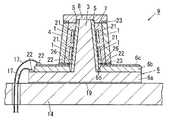
本実施形態の発光装置10は、青色光を放射する複数個の発光素子たるLEDチップ1を備えた光源部9と、該光源部9の少なくとも一部を内部に配し、内面2cが光源部9からの光を外部に反射する反射面を回転面とする光学素子2と、を有する発光装置10である。特に、光学素子2の前記内部における光源部9は、前記回転面の回転軸Aに沿って長手方向が配される多角形状の柱状体3と、該柱状体3を囲み、該柱状体3の側面3aに配置されたLEDチップ1が発光する青色光の一部を吸収して波長変換した黄色光を発する光変換部材4とを有している。  The light-emittingdevice 10 of the present embodiment includes alight source unit 9 including anLED chip 1 as a plurality of light-emitting elements that emit blue light, and at least a part of thelight source unit 9 is disposed inside, and an inner surface 2c is a light source unit. 9 is a light-emittingdevice 10 having anoptical element 2 having a reflecting surface that reflects light from 9 to the outside as a rotating surface. In particular, thelight source unit 9 in the inside of theoptical element 2 surrounds thecolumnar body 3 with a polygonalcolumnar body 3 whose longitudinal direction is arranged along the rotation axis A of the rotation surface, and thecolumnar body 3. It has thelight conversion member 4 which emits the yellow light which absorbed a part of blue light whichLED chip 1 arrange | positioned in theside surface 3a light-emitted, and wavelength-converted.

より具体的には、本実施形態の発光装置10は、図1(a)の断面図に示すように、発光装置10の筐体14が有底円筒状に形成されており、有底円筒状の内底面の中央部に光源部9を配置している。光源部9は、筐体14の底壁に対して固定螺子15により螺子止めされている。ここで、光源部9と、筐体14の内底面との間には熱伝導性シート19を挟み込んでいる。また、筐体14内には、光源部9から放出される光の配光を制御する上述の光学素子2が収納されている。光学素子2は、椀状に形成され、底部に光源部9が挿入される開口部2aを有している。椀状の光学素子2は、内面2cが光源部9からの光を外部に反射する回転放物面形状の回転面となっており、光学素子2の焦点Fを前記回転面の回転軸Aにおける後述する光源部9の複数個のLEDチップ1間における略中心と一致するように配置させている。光学素子2は、アルミニウム材料で構成され、アルミニウム蒸着あるは銀蒸着などの鏡面加工処理が施された反射面を有している。  More specifically, in thelight emitting device 10 of the present embodiment, as shown in the cross-sectional view of FIG. 1A, thecasing 14 of thelight emitting device 10 is formed in a bottomed cylindrical shape, and the bottomed cylindrical shape is Alight source unit 9 is arranged at the center of the inner bottom surface. Thelight source unit 9 is screwed to the bottom wall of thehousing 14 by a fixingscrew 15. Here, a heatconductive sheet 19 is sandwiched between thelight source unit 9 and the inner bottom surface of thehousing 14. Thehousing 14 houses the above-describedoptical element 2 that controls the light distribution of the light emitted from thelight source unit 9. Theoptical element 2 is formed in a bowl shape and has anopening 2a into which thelight source unit 9 is inserted at the bottom. In the bowl-shapedoptical element 2, the inner surface 2 c is a rotating paraboloid-shaped rotating surface that reflects light from thelight source unit 9 to the outside, and the focal point F of theoptical element 2 is on the rotation axis A of the rotating surface. It arrange | positions so that it may correspond with the approximate center between the someLED chips 1 of thelight source part 9 mentioned later. Theoptical element 2 is made of an aluminum material, and has a reflective surface that has been subjected to mirror finishing such as aluminum deposition or silver deposition.

また、光源部9からの光を外部に放射する光学素子2の開口径の大きい開口部側は、開口端から突出した外鍔部2bが設けられている。光学素子2の外鍔部2bは、外鍔部2b上に周部を重ねて設けた透光性のアクリル樹脂からなる円板状の透光性カバー11と共に、取付枠12により筐体14との間で狭持させ、複数本(ここでは、2本)の取付螺子13で取付け固定している。  Further, anouter flange portion 2b that protrudes from the opening end is provided on the opening side of theoptical element 2 that radiates light from thelight source unit 9 to the outside. Theouter flange portion 2b of theoptical element 2 is attached to thecasing 14 by a mountingframe 12 together with a disc-shapedtranslucent cover 11 made of a translucent acrylic resin provided with a circumferential portion overlapped on theouter flange portion 2b. And are fixed by a plurality of (two in this case) mounting screws 13.

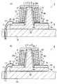
光源部9は、図1(b)に示すように、配線基板6の中央部に立設した多角形状の柱状体3と、柱状体3の各側面3aそれぞれ配置され各別に複数個のLEDチップ1が実装された複数枚の実装基板5と、柱状体3の長手方向に沿って柱状体3の外周を覆うように配置される円筒形状の光変換部材4とを備えている。また、柱状体3と光変換部材4との間には、LEDチップ1を被覆するシリコーン樹脂からなる透光性部材7が設けられている。ここで、配線基板6は、円板状に形成されており、アルミニウム材料からなる金属部6aにガラスエポキシ樹脂基板などからなる絶縁部6bが重ね合わされ、絶縁部6b上に配線パターン6cが形成されている。柱状体3は、配線基板6の中央部で立設できるように、配線基板6の金属部6bと熱伝導率の高い熱硬化型の接着剤からなる接合部20で接合してある。  As shown in FIG. 1B, thelight source unit 9 is arranged in a polygonalcolumnar body 3 erected at the center of thewiring substrate 6, and eachside surface 3 a of thecolumnar body 3. 1 is mounted, and a cylindricallight conversion member 4 disposed so as to cover the outer periphery of thecolumnar body 3 along the longitudinal direction of thecolumnar body 3. Further, atranslucent member 7 made of a silicone resin that covers theLED chip 1 is provided between thecolumnar body 3 and thelight conversion member 4. Here, thewiring substrate 6 is formed in a disk shape, and an insulatingportion 6b made of a glass epoxy resin substrate or the like is superimposed on ametal portion 6a made of an aluminum material, and awiring pattern 6c is formed on the insulatingportion 6b. ing. Thecolumnar body 3 is bonded to themetal portion 6b of thewiring board 6 by abonding portion 20 made of a thermosetting adhesive having a high thermal conductivity so that thecolumnar body 3 can be erected at the center of thewiring board 6.

LEDチップ1が実装された実装基板5が配置される本実施形態の柱状体3は、四角柱状の柱状体3の各側面3aの形状が実装基板5と略相似形で、かつ実装基板5を保持できる大きさとしている。また、柱状体3は、銅材料からなり、柱状体3の各側面3aと実装基板5とを、柱状体3を金属部6aに固定させたものと同じ接着剤からなる接合部20を用いて固定している。  In thecolumnar body 3 of the present embodiment on which the mountingsubstrate 5 on which theLED chip 1 is mounted is disposed, the shape of eachside surface 3a of the rectangular columnarcolumnar body 3 is substantially similar to that of the mountingsubstrate 5, and the mountingsubstrate 5 is The size can be held. Further, thecolumnar body 3 is made of a copper material, and theside surface 3a of thecolumnar body 3 and the mountingsubstrate 5 are used by using ajoint portion 20 made of the same adhesive as that in which thecolumnar body 3 is fixed to themetal portion 6a. It is fixed.

実装基板5は、図2で示すように、LEDチップ1が一表面5a側に搭載される長尺状の矩形平板に形成されている。実装基板5は、実装基板5の長辺が、数個(ここでは、2個)のLEDチップ1同士が接触しない間隔で配置可能であり、短辺が、1つのLEDチップ1を実装可能な大きさにしている。ここで、LEDチップ1間の中心は、実装基板5の長尺方向の中心よりも一方の短辺側にずれて配置させている。  As shown in FIG. 2, the mountingsubstrate 5 is formed in a long rectangular plate on which theLED chip 1 is mounted on the onesurface 5a side. The mountingsubstrate 5 can be arranged such that the long sides of the mountingsubstrate 5 are spaced apart from each other by several (here, two)LED chips 1 and the short side can mount oneLED chip 1. It is in size. Here, the center between theLED chips 1 is shifted from the center in the longitudinal direction of the mountingsubstrate 5 toward one short side.

本実施形態では、実装基板5をアルミナセラミック基板を用いて構成させており、実装基板5の一表面5a側に、NiメッキおよびAuメッキが形成されて、LEDチップ1と電気的に接続させる導体パターン5cを備えている。また、導体パターン5cの端部には、各LEDチップ1と電気的にされ給電させるための一対のランド5d,5dが形成されている。複数個のLEDチップ1は、実装基板5の一表面5a側に設けられた導体パターン5cによって直列接続されている。一対のランド5d,5dは、LEDチップ1間の中心が、片寄っている実装基板5の一方の短辺と反対の他方の短辺側に設けられている。また、実装基板5の一表面5aと反対の他表面5bの略全面にも、NiメッキおよびAuメッキを形成させて、矩形状の導体パターン5eとしている。  In the present embodiment, the mountingsubstrate 5 is configured using an alumina ceramic substrate, and Ni plating and Au plating are formed on the onesurface 5a side of the mountingsubstrate 5 so as to be electrically connected to theLED chip 1. Apattern 5c is provided. In addition, a pair oflands 5d and 5d are formed at the end of theconductor pattern 5c to be electrically connected to theLED chips 1 and to supply power. The plurality ofLED chips 1 are connected in series by aconductor pattern 5 c provided on the onesurface 5 a side of the mountingsubstrate 5. The pair oflands 5d, 5d are provided on the other short side opposite to the one short side of the mountingsubstrate 5 where the center between theLED chips 1 is offset. Further, Ni plating and Au plating are formed on substantially the entireother surface 5b opposite to the onesurface 5a of the mountingsubstrate 5 to form arectangular conductor pattern 5e.

実装基板5に実装される複数個のLEDチップ1は、それぞれ矩形平板の実装基板5の一表面5a側に形成された導体パターン5cと電気的に接続して固定できるように複数個の金属バンプ(たとえば、Auバンプや半田バンプなど)21(図1(b)を参照)を用いてフリップチップ実装している。なお、各LEDチップ1は、青色光が発光可能な発光素子として、絶縁性基板(たとえば、サファイア基板やスピネル基板など)上にp型およびn型の窒化ガリウム系化合物半導体層が形成されてpn接合を備え、該LEDチップ1の同一面側にp型およびn型の各窒化ガリウム系化合物半導体層と接続される正負の各電極を備えている。  The plurality ofLED chips 1 mounted on the mountingsubstrate 5 are each formed of a plurality of metal bumps so as to be electrically connected and fixed to theconductor pattern 5c formed on the onesurface 5a side of the rectangularflat mounting substrate 5. Flip chip mounting is performed using 21 (see, for example, Au bump, solder bump, etc.) 21 (see FIG. 1B). EachLED chip 1 has a p-type and n-type gallium nitride compound semiconductor layer formed on an insulating substrate (for example, a sapphire substrate, a spinel substrate, etc.) as a light emitting element capable of emitting blue light. Each of the positive and negative electrodes connected to the p-type and n-type gallium nitride compound semiconductor layers is provided on the same surface side of theLED chip 1.

柱状体3の側面3aに配置される実装基板5の一表面5a側の導体パターン5cにおける一対のランド5d,5dは、Au材料からなる金属配線25で、円板状の配線基板6の絶縁部6b上に形成された複数個の配線パターン6cとそれぞれ電気的に接続される。配線基板6上の複数個の配線パターン6cには、配線パターン6cの端部に設けられた電極端子6e,6e(図3(b),(d)を参照)に発光装置10外の電源ユニット(図示せず)からの一対の電源線17,17がそれぞれ半田部22,22によって電気的に接続されている。  A pair oflands 5d and 5d in theconductor pattern 5c on the onesurface 5a side of the mountingsubstrate 5 arranged on theside surface 3a of thecolumnar body 3 aremetal wirings 25 made of Au material, and an insulating portion of the disk-shapedwiring substrate 6 Each of thewiring patterns 6c formed on 6b is electrically connected. The plurality ofwiring patterns 6c on thewiring board 6 include power terminals outside thelight emitting device 10 onelectrode terminals 6e and 6e (see FIGS. 3B and 3D) provided at the ends of thewiring pattern 6c. A pair ofpower lines 17 and 17 from (not shown) are electrically connected bysolder portions 22 and 22, respectively.

また、光源部9は、LEDチップ1が側面3aに配置され、前記回転面の回転軸Aに沿って長手方向が配される柱状体3が立設された配線基板6上に、たとえば、シリコーン樹脂などの固定材23で円筒形状の光変換部材4を固着しており、光変換部材4の円筒形状における中心軸を回転軸Aと略一致して配置させている。  Thelight source unit 9 includes, for example, silicone on awiring board 6 in which theLED chip 1 is disposed on theside surface 3a and thecolumnar body 3 is disposed in the longitudinal direction along the rotation axis A of the rotation surface. The cylindricallight conversion member 4 is fixed by a fixingmaterial 23 such as a resin, and the central axis of thelight conversion member 4 in the cylindrical shape is arranged substantially coincident with the rotation axis A.

光学素子2の回転軸Aに沿った光変換部材4の長さは、配線基板6に立設された柱状体3の長手方向の長さと略同じにしており、円筒形状の光変換部材4の内部に柱状体3の各側面3aに配置された複数個のLEDチップ1が配置されることになる。なお、本実施形態の円筒形状の光変換部材4の内側と柱状体3との間には、シリコーン樹脂からなる透光性部材7が充填されており、柱状体3の側面3aに配置されたLEDチップ1を被覆されている。  The length of thelight conversion member 4 along the rotation axis A of theoptical element 2 is substantially the same as the length in the longitudinal direction of thecolumnar body 3 erected on thewiring board 6. A plurality ofLED chips 1 arranged on eachside surface 3a of thecolumnar body 3 are arranged inside. In addition, between the inner side of the cylindricallight conversion member 4 of this embodiment and thecolumnar body 3, thetranslucent member 7 which consists of silicone resin is filled, and it has arrange | positioned at theside surface 3a of thecolumnar body 3. TheLED chip 1 is covered.

光変換部材4には、シリコーン樹脂中にLEDチップ1から放出された青色光により励起されて、青色光の励起光よりも長波長の黄色光を放出する粒子状の蛍光体を含有させたものを用いている。  Thelight conversion member 4 contains a particulate phosphor that is excited by the blue light emitted from theLED chip 1 and emits yellow light having a longer wavelength than the excitation light of the blue light in the silicone resin. Is used.

本実施形態の発光装置10では、柱状体3の長手方向の先端部3bに柱状体3を覆って設けられ、先端部3bと対向する面側に光を反射するアルミニウムからなる円板状の反射部材8を設けている。したがって、円板状の反射部材8は、柱状体3側が、LEDチップ1や光変換部材4からの光を反射することができる。反射部材8の柱状体3側の中央部には、窪みが設けられており、柱状体3の先端部3bを反射部材8の窪みに挿入して固定している。発光装置10は、外部からLEDチップ1に給電することにより光源部9を点灯させ、光学素子2を用いて配光制御性を確保しつつ、照度むらがより少ない均一な白色光を放射することができる。  In thelight emitting device 10 of the present embodiment, a disk-shaped reflection made of aluminum that is provided on thefront end portion 3b in the longitudinal direction of thecolumnar body 3 so as to cover thecolumnar body 3 and reflects light on the surface facing thefront end portion 3b. Amember 8 is provided. Therefore, the disk-shaped reflectingmember 8 can reflect the light from theLED chip 1 and thelight converting member 4 on thecolumnar body 3 side. A recess is provided in the center of the reflectingmember 8 on thecolumnar body 3 side, and thetip 3b of thecolumnar body 3 is inserted into the recess of the reflectingmember 8 and fixed. Thelight emitting device 10 emits uniform white light with less illuminance unevenness while lighting thelight source unit 9 by supplying power to theLED chip 1 from the outside and ensuring the light distribution controllability using theoptical element 2. Can do.

以下、本実施形態の発光装置10を製造工程について説明する。  Hereinafter, the manufacturing process of thelight emitting device 10 of the present embodiment will be described.

本願の発光装置10の光源部9を構成するため、図3(a)に示す円板状の金属部6aの中央部に四角柱形状の柱状体3を、接着剤からなる接合部20(図1(b)を参照)を用いて接合することで立設させる。柱状体3が立設した配線基板6の金属部6a上に、金属部6aと外形が略同じ円板状であって、中央部に柱状体3を挿入する柱状体3より大きく柱状体3の外形と相似形の開口部を備えた絶縁部6bを重ね合わせる。なお、絶縁部6bの表面には、配線パターン6cや配線パターン6cの端部に設けられた電極端子6e,6eが予め形成されている。これにより、柱状体3を備えた配線基板6を形成することができる。  In order to constitute thelight source unit 9 of thelight emitting device 10 of the present application, the rectangularcolumnar body 3 is formed at the center of the disk-shapedmetal unit 6a shown in FIG. 1 (see (b)). On themetal part 6a of thewiring board 6 on which thecolumnar body 3 is erected, the outer shape of thecolumnar body 3 is larger than that of thecolumnar body 3 which is substantially the same disk shape as themetal part 6a and into which thecolumnar body 3 is inserted. The insulatingportion 6b having an opening similar to the outer shape is overlapped. Note that, on the surface of the insulatingportion 6b, thewiring pattern 6c andelectrode terminals 6e and 6e provided at the ends of thewiring pattern 6c are formed in advance. Thereby, thewiring board 6 provided with thecolumnar body 3 can be formed.

その後、LEDチップ1を一表面5aに実装した実装基板5の他表面5b側に接合部20となる接着剤を塗布し、柱状体3の側面3aと配線基板6の絶縁部6bとの隙間に形成される凹部6dに、実装基板5を挿入して柱状体3の側面3aに付着させる(図3(b)を参照)。  Thereafter, an adhesive to be thejoint portion 20 is applied to theother surface 5b side of the mountingsubstrate 5 on which theLED chip 1 is mounted on onesurface 5a, and the gap between theside surface 3a of thecolumnar body 3 and the insulatingportion 6b of thewiring substrate 6 is applied. The mountingsubstrate 5 is inserted into the formedrecess 6d and adhered to theside surface 3a of the columnar body 3 (see FIG. 3B).

次に、図3(c)に示す平板状冶具24の窪み(図示せず)内に柱状体3の先端部3bおよび各実装基板5の先端部側(図3(c)の上側)を収納させる。この状態で配線基板6などを加熱し、前記接着剤を加熱硬化させることで、柱状体3の各側面3aに各実装基板5をそれぞれ固定する。  Next, thefront end portion 3b of thecolumnar body 3 and the front end portion side of each mounting substrate 5 (upper side in FIG. 3C) are accommodated in the recesses (not shown) of theflat jig 24 shown in FIG. Let In this state, thewiring board 6 and the like are heated to heat and cure the adhesive, thereby fixing the mountingboards 5 to the side surfaces 3a of thecolumnar body 3, respectively.

その後、平板状冶具24を取り除き、各LEDチップ1に外部から給電できるように各実装基板5のランド5dと配線基板6の配線パターン6cとを金属配線などにより電気的に接続させる(図示していない)。次に、円筒形状の光変換部材4の周端部に、固定材23となるシリコーン樹脂を塗布して柱状体3を囲むように配線基板6上に設置し加熱硬化して固定材23により固定する。  Thereafter, theflat jig 24 is removed, and theland 5d of each mountingsubstrate 5 and thewiring pattern 6c of thewiring substrate 6 are electrically connected to eachLED chip 1 by metal wiring or the like so that power can be supplied from the outside (not shown). Absent). Next, a silicone resin to be the fixingmaterial 23 is applied to the peripheral end portion of the cylindricallight conversion member 4, is placed on thewiring board 6 so as to surround thecolumnar body 3, is heated and cured, and is fixed by the fixingmaterial 23. To do.

続いて、減圧環境下において、光変換部材4と各実装基板5が側面3aに固定され配線基板6から立設した柱状体3との間に、透光性部材7となるシリコーン樹脂を各LEDチップ1が被覆されるまで充填させる(図1(b)を参照)。  Subsequently, in a reduced pressure environment, a silicone resin serving as atranslucent member 7 is placed between thelight conversion member 4 and thecolumnar body 3 erected from thewiring substrate 6 with each mountingsubstrate 5 fixed to theside surface 3a. Fill until thechip 1 is covered (see FIG. 1B).

透光性部材7となるシリコーン樹脂が充填され、光変換部材4および実装基板5が固定された柱状体3の先端部3bに、反射部材8を固定材23となるシリコーン樹脂を介して配置し、前記各シリコーン樹脂を加熱硬化させることで光源部9を形成させることができる(図3(d)を参照)。  Thereflective member 8 is disposed on thetip 3b of thecolumnar body 3 filled with the silicone resin to be thetranslucent member 7 and to which thelight conversion member 4 and the mountingsubstrate 5 are fixed via the silicone resin to be the fixingmaterial 23. Thelight source unit 9 can be formed by heating and curing the silicone resins (see FIG. 3D).

このような光源部9を、図1(a)で示す円板状の配線基板6の周端部で、柱状体3が立設された一表面側から有底円筒状に形成された筐体14の底壁に対して、熱伝導性シート19を介して圧接して固定螺子15により螺子止めする。  Such alight source portion 9 is a casing formed in a cylindrical shape with a bottom from the one surface side where thecolumnar body 3 is erected at the peripheral end portion of the disc-like wiring board 6 shown in FIG. Thebottom wall 14 is pressed against the bottom wall via a heatconductive sheet 19 and fixed with a fixingscrew 15.

続いて、光源部9から放出される光を反射させて配光を制御する光学素子2を、筐体14内に収納し、光学素子2の開口縁から突出した外鍔部2bと、筐体14の開口内部を保護する透光性カバー11とを狭持する形で筐体14の開口縁との間に円環状の取付枠12を筐体14に対して複数本(ここでは、2本)の取付螺子13により固定する。これにより、光学素子2を用いて配光制御しつつ、発光装置10から照射された光の照度むらを抑制することが可能な発光装置10を製造することができる。  Subsequently, theoptical element 2 that controls the light distribution by reflecting the light emitted from thelight source unit 9 is housed in thecasing 14, and thecasing 2 b protruding from the opening edge of theoptical element 2, and the casing A plurality of annular mounting frames 12 with respect to the casing 14 (two here) are provided between the opening edges of thecasing 14 so as to sandwich thetranslucent cover 11 that protects the inside of the opening of thecasing 14. ). Accordingly, it is possible to manufacture thelight emitting device 10 that can suppress unevenness in the illuminance of the light emitted from thelight emitting device 10 while controlling the light distribution using theoptical element 2.

以下、本実施形態の発光装置10に用いられる各構成について詳述する。  Hereinafter, each component used for the light-emittingdevice 10 of this embodiment is explained in full detail.

本実施形態における発光素子は、光変換部材4が吸収して波長変換することができる光を発光可能な半導体を用いた発光素子である。発光素子として、たとえば、青色光や紫外線を高出力に発光可能なpn接合を備えた窒化ガリウム系化合物半導体からなるLEDチップ1などを利用することができる。LEDチップ1は、たとえば、結晶成長用基板としてサファイア、スピネル、GaN、SiCや酸化亜鉛などの基板を用い、該基板上にp型およびn型の窒化ガリウム系化合物半導体層がそれぞれ形成され、前記p型およびn型窒化ガリウム系化合物半導体層と各別に電気的に接続される正負の各電極を備えたものが挙げられる。  The light emitting element in the present embodiment is a light emitting element using a semiconductor capable of emitting light that can be absorbed and converted by thelight conversion member 4. As the light emitting element, for example, theLED chip 1 made of a gallium nitride compound semiconductor having a pn junction capable of emitting blue light or ultraviolet light with high output can be used. TheLED chip 1 uses, for example, a substrate such as sapphire, spinel, GaN, SiC or zinc oxide as a crystal growth substrate, and p-type and n-type gallium nitride compound semiconductor layers are formed on the substrate, respectively. Examples include those having positive and negative electrodes electrically connected to the p-type and n-type gallium nitride compound semiconductor layers.

図1(b)に示す発光装置10の光源部9には、同一面側に正負の各電極を形成させたLEDチップ1を用い、LEDチップ1を実装基板5にフェースダウンで実装しているが、図4(b)で示すように発光装置10の光源部9は、同一面側に正負の各電極を形成させたLEDチップ1を用い、LEDチップ1を実装基板5にフェースアップで実装してもよい。  In thelight source unit 9 of thelight emitting device 10 shown in FIG. 1B, theLED chip 1 in which positive and negative electrodes are formed on the same surface side is used, and theLED chip 1 is mounted on the mountingsubstrate 5 face down. However, as shown in FIG. 4B, thelight source unit 9 of thelight emitting device 10 uses theLED chip 1 in which positive and negative electrodes are formed on the same surface side, and theLED chip 1 is mounted on the mountingsubstrate 5 face up. May be.

LEDチップ1がフェースダウンで実装される場合、LEDチップ1の正負の各電極と、実装基板5の各導体パターン5c,5cとを金属バンプ(たとえば、Auバンプや半田バンプなど)21やAgペーストなどを介して電気的に接続させることができる。また、LEDチップ1がフェースアップで実装される場合、LEDチップ1を実装基板5にエポキシ樹脂等で固定させた後、LEDチップ1の正負の各電極と、実装基板5の各導体パターン5c,5cとをそれぞれワイヤ(たとえば、金線やアルミニウム線)16で電気的に接続させればよい。  When theLED chip 1 is mounted face down, the positive and negative electrodes of theLED chip 1 and theconductor patterns 5c and 5c of the mountingsubstrate 5 are connected to metal bumps 21 (for example, Au bumps or solder bumps) 21 or Ag paste. It can be electrically connected through such as. When theLED chip 1 is mounted face up, after fixing theLED chip 1 to the mountingsubstrate 5 with epoxy resin or the like, the positive and negative electrodes of theLED chip 1 and theconductor patterns 5c of the mountingsubstrate 5 are provided. What is necessary is just to electrically connect 5c with the wire (for example, gold wire or aluminum wire) 16, respectively.

また、発光装置10は、導電性基板(たとえば、窒化ガリウム基板、SiC基板や酸化亜鉛基板など)を用い、LEDチップ1の厚み方向の両面に正負の各電極が形成された発光素子を用いてもよい。図4(a)に示す発光装置10の光源部9は、厚み方向の両面に正負の各電極が形成されたLEDチップ1を実装基板5上にAuSn、Agペースト等で固定させ実装基板5の一方の導体パターン5cとLEDチップ1の一方の電極と電気的に接続させた後、LEDチップ1の他方の電極と、実装基板5の他方の導体パターン5cとをワイヤ16で電気的に接続させればよい。なお、図4は、図1と同様の構成要素には同一の符号を付している。  The light-emittingdevice 10 uses a light-emitting element in which positive and negative electrodes are formed on both surfaces in the thickness direction of theLED chip 1 using a conductive substrate (for example, a gallium nitride substrate, a SiC substrate, or a zinc oxide substrate). Also good. Thelight source unit 9 of thelight emitting device 10 shown in FIG. 4A is configured such that theLED chip 1 having positive and negative electrodes formed on both surfaces in the thickness direction is fixed on the mountingsubstrate 5 with AuSn, Ag paste or the like. After electrically connecting oneconductor pattern 5 c and one electrode of theLED chip 1, the other electrode of theLED chip 1 and theother conductor pattern 5 c of the mountingsubstrate 5 are electrically connected by awire 16. Just do it. In FIG. 4, the same components as those in FIG.

LEDチップ1は、同種のものを用いてもよいし、異なる発光波長を発光する複数個のLEDチップ1を用いてもよい。たとえば、発光色を調整するなどの目的で青色光が発光可能なLEDチップ1に加え、赤色光が発光可能なLEDチップを備えていてもよい。また、LEDチップ1は、所望に応じて同一の実装基板5上に複数個設けることができ、各々を実装基板5上に設けた導体パターン5cを用いて電気的に直列接続、並列接続や直並列接続させてもよい。なお、LEDチップ1は、実装基板5上にサブマウント(図示せず)を介して実装させてもよい。  The same type ofLED chip 1 may be used, or a plurality ofLED chips 1 that emit different emission wavelengths may be used. For example, in addition to theLED chip 1 capable of emitting blue light for the purpose of adjusting the emission color, an LED chip capable of emitting red light may be provided. Further, a plurality ofLED chips 1 can be provided on the same mountingsubstrate 5 as desired, and each of them is electrically connected in series, in parallel or directly using aconductor pattern 5c provided on the mountingsubstrate 5. You may connect in parallel. TheLED chip 1 may be mounted on the mountingsubstrate 5 via a submount (not shown).

本実施形態に用いられる光学素子2は、光源部9からの光を配光制御して外部に反射することが可能なものである。  Theoptical element 2 used in this embodiment is capable of controlling the light distribution from thelight source unit 9 and reflecting it to the outside.

光学素子2は、光源部9から放射された光を透光性カバー11側へ反射させ狭角配光などが得られるように内面2cの形状が設計されており、内面2cが柱状体3の側面3aに配置させたLEDチップ1間の略中心を焦点Fとする回転放物面状に形成されている。光学素子2の内面2cの形状は、放物面状だけでなく、回転体となる楕円面状や双曲面状に形成させてもよい。また、光学素子2は、所望の配光特性に応じて、光源部9から離れるにつれて開口面積が徐々に大きくなる複数種類の回転面を備えた異なる形状の組み合わせからなる椀状の形状などに形成することもできる。  Theoptical element 2 is designed to have an inner surface 2 c that reflects light emitted from thelight source unit 9 toward thetranslucent cover 11 to obtain a narrow-angle light distribution, and the inner surface 2 c is thecolumnar body 3. It is formed in the shape of a rotating paraboloid with the focal point F as the approximate center between theLED chips 1 arranged on theside surface 3a. The shape of the inner surface 2c of theoptical element 2 may be formed not only in the shape of a paraboloid but also in the shape of an ellipse or hyperboloid as a rotating body. Further, theoptical element 2 is formed in a bowl-like shape composed of a combination of different shapes having a plurality of types of rotating surfaces whose opening area gradually increases as the distance from thelight source unit 9 increases according to desired light distribution characteristics. You can also

光学素子2の材料としては、たとえば、LEDチップ1や光変換部材4から放射される光の波長を効率よく反射する金属(たとえば、アルミニウムやステンレスなど)や高耐熱性の樹脂(たとえば、PBTなど)などが挙げられる。また、光学素子2の内面2cは、発光装置10からの光を効率よく反射させるため、所望に応じて、アルミニウム蒸着や銀蒸着などの鏡面加工処理を施してもよいし、白色などの塗料を塗布することもできる。  Examples of the material of theoptical element 2 include a metal (for example, aluminum and stainless steel) that efficiently reflects the wavelength of light emitted from theLED chip 1 and thelight conversion member 4 and a high heat resistant resin (for example, PBT). ) And the like. In addition, the inner surface 2c of theoptical element 2 may be subjected to mirror processing such as aluminum vapor deposition or silver vapor deposition as desired in order to efficiently reflect the light from thelight emitting device 10, or a paint such as white may be used. It can also be applied.

本実施形態に用いられる柱状体3は、光源部9の一部を構成し、柱状体3の側面3aにLEDチップ1を配置することができるものである。  Thecolumnar body 3 used in the present embodiment constitutes a part of thelight source unit 9, and theLED chip 1 can be disposed on theside surface 3 a of thecolumnar body 3.

柱状体3の各側面3aに、LEDチップ1が実装された実装基板5を配置する場合は、側面3aの形状が実装基板5と相似形でかつ実装基板5を保持できる大きさとすることが好ましい。また、柱状体3の各側面3aに実装基板5を熱伝導率の高い熱硬化型の接着剤からなる接合部20で固定する場合、接合部20の材料としては、たとえば、シリカやAgフィラーが含有されたエポキシ樹脂などが挙げられ、半田を用いてもよい。  When the mountingsubstrate 5 on which theLED chip 1 is mounted is disposed on eachside surface 3 a of thecolumnar body 3, it is preferable that the shape of theside surface 3 a is similar to the mountingsubstrate 5 and is large enough to hold the mountingsubstrate 5. . Moreover, when fixing the mountingsubstrate 5 to eachside surface 3a of thecolumnar body 3 with thejoint part 20 which consists of a thermosetting adhesive with high thermal conductivity, as a material of thejoint part 20, for example, silica or Ag filler is used. Examples thereof include an epoxy resin, and solder may be used.

柱状体3は、配線基板6に嵌め込みや接着などにより立設させてもよいし、柱状体3と配線基板6とを一体的に形成させてもよい。また、柱状体3の材質としては、LEDチップ1で生じた熱を外部に放熱できるように熱伝導性の高いなど各種合金、窒化アルミニウム、銅やアルミニウムの金属材料などを用いることができる。  Thecolumnar body 3 may be erected on thewiring substrate 6 by fitting or bonding, or thecolumnar body 3 and thewiring substrate 6 may be integrally formed. Moreover, as a material of thecolumnar body 3, various alloys such as high thermal conductivity such as heat generated in theLED chip 1 can be dissipated to the outside, aluminum nitride, copper, and a metal material of aluminum can be used.

なお、柱状体3の長手方向と垂直な横断面は、正方形だけでなく適宜多角形状とすることができる。また、柱状体3の各側面3aの大きさは、必ずしも同じ大きさで形成させる必要もなく、たとえば、柱状体3の外形を六角錐台形状とし、一つ置きに3つの側面3aを他の3つの側面3aより大きく形成させてもよい。また、柱状体3の側面3aに配置されるLEDチップ1は、光学素子2から必要とする配光パターンが得られる限り、必ずしも全ての各側面3aに同様に配置させる必要もない。  In addition, the cross section perpendicular | vertical to the longitudinal direction of thecolumnar body 3 can be not only a square but polygonal shape suitably. Further, the size of eachside surface 3a of thecolumnar body 3 does not necessarily have to be the same size. For example, thecolumnar body 3 has an outer shape of a hexagonal frustum and everyother side surface 3a has a different shape. It may be formed larger than the threeside surfaces 3a. Further, theLED chip 1 disposed on theside surface 3a of thecolumnar body 3 does not necessarily need to be disposed in the same manner on all the side surfaces 3a as long as the required light distribution pattern is obtained from theoptical element 2.

また、LEDチップ1は、必ずしも実装基板5に設けられる必要もなく、図5(a)の発光装置10の光源部9に示すように表面に導体パターン5cを形成させた柱状体3に直接実装させてもよい。なお、柱状体3をアルミニウムや銅などの金属により形成させる場合、導体パターン5cと柱状体3の側面3aとの間に適宜の絶縁層を設ければよい。  Further, theLED chip 1 is not necessarily provided on the mountingsubstrate 5, and is directly mounted on thecolumnar body 3 having theconductor pattern 5 c formed on the surface as shown in thelight source unit 9 of thelight emitting device 10 of FIG. You may let them. When thecolumnar body 3 is formed of a metal such as aluminum or copper, an appropriate insulating layer may be provided between theconductor pattern 5 c and theside surface 3 a of thecolumnar body 3.

さらに、柱状体3は、必ずしも1体で形成させる必要もなく、各側面3aに配置されるLEDチップ1を損傷することなく、ダイボンダなどの実装装置で実装できるように、たとえば、図5(b)に示すように、発光装置10の回転軸Aをとおる面で対称に2分割してもよい。2分割で構成される柱状体3は、分割面同士を密着するように構成し、配線基板6に立設して固定すればよい。柱状体3は、2分割だけでなく必要に応じて複数個に分けて形成することができる。なお、図5は、図1と同様の構成要素には同一の符号を付している。  Further, thecolumnar body 3 is not necessarily formed as a single body, and can be mounted by a mounting apparatus such as a die bonder without damaging theLED chip 1 disposed on eachside surface 3a. ), The light-emittingdevice 10 may be divided in two symmetrically on the plane passing through the rotation axis A. Thecolumnar body 3 composed of two parts may be configured so that the divided surfaces are in close contact with each other, and may be erected and fixed on thewiring board 6. Thecolumnar body 3 can be formed not only in two parts but also in a plurality of parts as required. In FIG. 5, the same components as those in FIG. 1 are denoted by the same reference numerals.

ところで、光学素子2は、一般的に、光学素子2の焦点Fを光源部9中心の擬似的な点光源に合わせて設計する。しかし、実際の光源部9は、ある大きさを持ち、光学素子2の焦点Fから離れるため、光源部9からの光が光学素子9で反射されても焦点がぼやけた光となる。このため、発光装置10では、光源部9からの光をできるだけ集光(狭角配光)するために、光を放射する光源部9の大きさが光学素子2の焦点Fに近いほど好ましい。  By the way, theoptical element 2 is generally designed so that the focal point F of theoptical element 2 matches a pseudo point light source at the center of thelight source unit 9. However, since the actuallight source unit 9 has a certain size and is away from the focal point F of theoptical element 2, even if the light from thelight source unit 9 is reflected by theoptical element 9, the light is blurred. For this reason, in the light-emittingdevice 10, in order to collect the light from thelight source unit 9 as much as possible (narrow-angle light distribution), it is preferable that the size of thelight source unit 9 that emits light is closer to the focal point F of theoptical element 2.

本実施形態の光源部9のLEDチップ1は、柱状体3の側面3aに備えられ、立体的に配置されている。そのため、光学素子2の焦点Fと、光を放射する光源部9との距離を、光学素子2の一端部に面光源としてLEDチップ1を配置させるものと比較して小さくでき、焦点のぼやけた光の割合を小さくすることができる。このような立体的な光源部9を備えた発光装置10は、主に光学素子2により配光制御された光で構成される照射パターンの主要部となる被照射面の中央の光成分を増加させ、より均一な照射パターンを得ることに寄与できる。  TheLED chip 1 of thelight source unit 9 of the present embodiment is provided on theside surface 3a of thecolumnar body 3 and is arranged three-dimensionally. Therefore, the distance between the focal point F of theoptical element 2 and thelight source unit 9 that emits light can be made smaller than that in which theLED chip 1 is arranged as a surface light source at one end of theoptical element 2, and the focal point is blurred. The proportion of light can be reduced. Thelight emitting device 10 having such a three-dimensionallight source unit 9 increases the light component at the center of the irradiated surface, which is the main part of the irradiation pattern mainly composed of light whose light distribution is controlled by theoptical element 2. Can contribute to obtaining a more uniform irradiation pattern.

本実施形態に用いられる光変換部材4は、光源部9の一部を構成し、光学素子2の回転軸Aに沿って長手方向が配される多角形状の柱状体3を囲み、該柱状体3の側面3aに配置されたLEDチップ1が発光する光の少なくとも一部を吸収して波長変換した光を発するものである。光変換部4は、たとえば、LEDチップ1が実装された実装基板5を備えた柱状体3の長手方向に沿って、柱状体3の外周を囲む円筒形状とすることができる。また、光変換部材4は、LEDチップ1が発光する光の少なくとも一部を吸収して波長変換した光を発するため、たとえば、シリコーン樹脂、アクリル樹脂、ポリカーボネート樹脂などの有機材料やガラスなど無機材料からなる透光性材料中に蛍光体を含有したものが挙げられる。  Thelight conversion member 4 used in the present embodiment constitutes a part of thelight source unit 9, surrounds the polygonalcolumnar body 3 whose longitudinal direction is arranged along the rotation axis A of theoptical element 2, and the columnar body. 3 emits light whose wavelength is converted by absorbing at least part of the light emitted by theLED chip 1 disposed on theside surface 3a. Thelight conversion part 4 can be made into the cylindrical shape surrounding the outer periphery of thecolumnar body 3 along the longitudinal direction of thecolumnar body 3 provided with the mountingsubstrate 5 on which theLED chip 1 is mounted, for example. In addition, thelight conversion member 4 absorbs at least a part of the light emitted from theLED chip 1 and emits light whose wavelength is converted. For example, thelight conversion member 4 is an organic material such as silicone resin, acrylic resin, or polycarbonate resin, or an inorganic material such as glass. The thing which contained the fluorescent substance in the translucent material which consists of is mentioned.

光変換部材4に用いられる前記蛍光体としては、たとえば、LEDチップ1から放出された青色光を吸収して黄色光を発光可能なものが挙げられる。前記蛍光体は、前記透光性材料中に均一に分散して含有させることができる。  Examples of the phosphor used in thelight conversion member 4 include those capable of absorbing blue light emitted from theLED chip 1 and emitting yellow light. The phosphor can be uniformly dispersed in the translucent material.

光変換部材4に用いられる前記蛍光体は、LEDチップ1から放出された光により励起されて、励起光よりも長波長の光を放出する粒子状の蛍光体(たとえば、青色光により励起され発光波長域がブロードな黄色系の光を放出する蛍光体や紫外線により励起され青色、緑色および赤色をそれぞれ発光可能な3種類の蛍光体など)を用いることができる。青色光を吸収して黄色光を発光する前記蛍光体としては、たとえば、Ceで付活されたYAl12、Ceで付活されたTbAl12などのアルミネート系の蛍光体のほか、Euが付活されたBaSiOなどのアルカリ土類珪酸塩系の蛍光体、CaBOClなどのファロボレート系の蛍光体などを採用することもできる。また、光変換部材4に含有される前記蛍光体は黄色蛍光体に限らず、緑色蛍光体あるいは橙色蛍光体や赤色蛍光体あるいはそれらの組み合わせの前記蛍光体を用いてもよい。たとえば、色調整や演色性を高めるなどの目的で複数種類の蛍光体を用いてもよく、本実施形態の黄色蛍光体の代わりに、赤色蛍光体と緑色蛍光体を含有させても、白色光を得ることができる。The phosphor used in thelight conversion member 4 is excited by light emitted from theLED chip 1 and emits light having a wavelength longer than that of the excitation light (for example, excited by blue light to emit light). A phosphor that emits yellow light having a broad wavelength range, or three types of phosphors that are excited by ultraviolet rays and can emit blue, green, and red, respectively) can be used. Examples of the phosphor that absorbs blue light and emits yellow light include aluminate-based phosphors such as Y3 Al5 O12 activated with Ce and Tb3 Al5 O12 activated with Ce. In addition to the phosphor, an alkaline earth silicate phosphor such as Ba2 SiO4 activated with Eu, and a faroborate phosphor such as Ca2 BO3 Cl2 can also be used. The phosphor contained in thelight conversion member 4 is not limited to a yellow phosphor, and a green phosphor, an orange phosphor, a red phosphor, or a combination thereof may be used. For example, a plurality of types of phosphors may be used for the purpose of improving color adjustment and color rendering, and white light can be used even if a red phosphor and a green phosphor are included instead of the yellow phosphor of this embodiment. Can be obtained.

ところで、発光装置10からの光を白色光にする場合、青色光を吸収して黄色光を放出する蛍光体が含有された樹脂で青色光を発光するLEDチップ1を被覆した白色LEDも知られており、本実施形態におけるLEDチップ1および光変換部材4を用いる代わりに、単に、白色LEDを用いる場合も考えられる。しかしながら、このような白色LEDを単に柱状体3の側面3aに配置させると、白色LED間は非発光部となるため、光源部9全体として輝度むらが生じ、発光装置10から放出される光に輝度むらが目立ってしまう恐れがある。また、複数個の白色LEDを用いた場合、各白色LED間のばらつきが目立ってしまう場合もある。特に、照明装置にまで用いられる高出力の発光装置10において、上述の補色となる光を混色させた白色LEDを用いた場合では、混色光の少しの色ずれが補色関係にずれるため、人間の目には、顕著に視認される傾向にある。  By the way, when making the light from the light-emittingdevice 10 white light, white LED which coat | coveredLED chip 1 which light-emits blue light with the resin containing the fluorescent substance which absorbs blue light and discharge | releases yellow light is also known. In addition, instead of using theLED chip 1 and thelight conversion member 4 in the present embodiment, a case of simply using a white LED may be considered. However, when such a white LED is simply arranged on theside surface 3a of thecolumnar body 3, since the white LED becomes a non-light emitting portion, unevenness in luminance occurs in thelight source unit 9 as a whole, and the light emitted from thelight emitting device 10 is reduced. There is a risk of uneven brightness. Moreover, when using several white LED, the dispersion | variation between each white LED may become conspicuous. In particular, in the high-output light-emittingdevice 10 used for the lighting device, in the case of using a white LED in which the above-described complementary color light is mixed, a slight color shift of the mixed color light shifts to a complementary color relationship. The eyes tend to be noticeable.

本実施形態の発光装置10においては、光源部9全体が光変換部材4で覆われており、かつLEDチップ1と光変換部材4との間に間隔を有しているため、柱状体3の異なる平面となる各側面3aに配置されたLEDチップ1間の前方や側面3aの同一平面側に配置されたLEDチップ1間の前方にあたる光変換部材4の部位にもLEDチップ1から発した光が到達し、白色光を発することができる。したがって、発光装置10は、光源部9全体がより均一な輝度分布となり、放射された光の色むらや輝度むらを改善することができる。  In thelight emitting device 10 of the present embodiment, the entirelight source unit 9 is covered with thelight conversion member 4 and there is a gap between theLED chip 1 and thelight conversion member 4. The light emitted from theLED chip 1 also in the portion of thelight conversion member 4 which is in front of theLED chips 1 arranged on the side surfaces 3a which are different planes and in front of theLED chip 1 arranged on the same plane side of theside surface 3a. Can reach and emit white light. Therefore, in thelight emitting device 10, the entirelight source unit 9 has a more uniform luminance distribution, and it is possible to improve color unevenness and luminance unevenness of emitted light.

また、本実施形態の発光装置10においては、光源部9から放射される光が、光学素子2によって反射され単純に回転軸Aに沿って外部に放射されるものだけでなく、光源部9から放射され光学素子2によって光源部9に再び向かう光もある。このような光源部9に向かう光は、光変換部材4に入射されたり、光変換部材4で反射されたりして、光学素子2により外部に再び放射される場合がある。  In thelight emitting device 10 according to the present embodiment, the light emitted from thelight source unit 9 is not only reflected from theoptical element 2 and simply emitted outside along the rotation axis A, but also from thelight source unit 9. There is also light that is emitted and travels again toward thelight source unit 9 by theoptical element 2. The light traveling toward thelight source unit 9 may be incident on thelight conversion member 4 or reflected by thelight conversion member 4 and may be emitted to the outside again by theoptical element 2.

したがって、発光装置10は、光源部9が多角形状の柱状体3の側面3aだけにLEDチップ1を配置させていても、柱状体3の隣接する側面3aに設けられたLEDチップ1間も光学素子2からの反射光などによって光変換部材4が発光などするため、放射された光の色むらや輝度むらを改善できると考えられる。  Therefore, in thelight emitting device 10, even if theLED chip 1 is disposed only on theside surface 3 a of the polygonalcolumnar body 3 in thelight source unit 9, theLED chip 1 provided on theadjacent side surface 3 a of thecolumnar body 3 is optically connected. Since thelight conversion member 4 emits light by reflected light from theelement 2 or the like, it is considered that unevenness in color and brightness of emitted light can be improved.

本実施形態では、LEDチップ1が発光した光を吸収して波長変換した光を発する光変換部材4の形状が、LEDチップ1から放射される光の指向特性やLEDチップ1が実装される実装基板5の配置形状に合わせて設計されるのではなく、発光装置10の光学素子2の形状に合わせて光学的に設計することができる。すなわち、発光装置10は、光変換部材4の形状を光学素子2の回転軸Aと略同一の軸で回転させた円柱形状や円錐台形状とすることで、光学素子2によって制御された照射パターンの照度むらや上述の色むらをさらに低減させることが可能となる。  In the present embodiment, the shape of thelight conversion member 4 that emits light whose wavelength has been converted by absorbing light emitted from theLED chip 1 is configured so that the directivity characteristics of light emitted from theLED chip 1 and theLED chip 1 are mounted. It is not designed according to the arrangement shape of thesubstrate 5 but can be optically designed according to the shape of theoptical element 2 of thelight emitting device 10. That is, the light-emittingdevice 10 has an irradiation pattern controlled by theoptical element 2 by changing the shape of thelight conversion member 4 to a columnar shape or a truncated cone shape rotated about the same axis as the rotation axis A of theoptical element 2. It is possible to further reduce the illuminance unevenness and the color unevenness described above.

本実施形態に用いられる実装基板5は、LEDチップ1を柱状体3の側面3aに配置することを容易にするために用いられるものであって、一表面5aに導電性パターン5cが形成された基板を用いることができる。  The mountingsubstrate 5 used in the present embodiment is used for facilitating the placement of theLED chip 1 on theside surface 3a of thecolumnar body 3, and theconductive pattern 5c is formed on the onesurface 5a. A substrate can be used.

より具体的には、実装基板5は、セラミック基板(たとえば、アルミナセラミック基板、窒化アルミニウム基板など)からなる絶縁性基板の一表面5a側に金属材料(たとえば、Auなど)を用いた導体パターン5cが形成されたものを用いることができる。なお、実装基板5はセラミック基板に限られず、ガラスエポキシ樹脂基板や表面に絶縁層(たとえば、ガラス結晶層や金属酸化物層など)が形成された金属からなる金属ベース基板を用いることもできる。さらに、実装基板5は、柱状体3を覆うように巻き付けることが可能なフレキシブル基板を利用することもできる。  More specifically, the mountingsubstrate 5 is aconductive pattern 5c using a metal material (for example, Au) on onesurface 5a side of an insulating substrate made of a ceramic substrate (for example, an alumina ceramic substrate, an aluminum nitride substrate, etc.). Can be used. The mountingsubstrate 5 is not limited to a ceramic substrate, and a metal base substrate made of a metal having an insulating layer (for example, a glass crystal layer or a metal oxide layer) formed on the surface thereof can be used. Furthermore, the mountingsubstrate 5 can use a flexible substrate that can be wound around thecolumnar body 3.

実装基板5上の複数個のLEDチップ1は、図2で示すように実装基板5の長尺方向に沿って1列である必要もなく、図6(a)の光源部9で示すように実装基板5の長尺方向に沿って、LEDチップ1を複数列(ここでは、2列)に配置させてもよい。また、図2や図6(a)で示すように実装基板5の長尺方向に沿って、複数個のLEDチップ1を一直線状に配置させてもよいし、図6(b)の光源部9で示すように、実装基板5の長尺方向に沿って複数個のLEDチップ1を千鳥足状に配置させてもよい。これにより、LEDチップ1の側方から放射される放射光が隣接配置されるLEDチップ1へ吸収されることを抑制し、吸収損失を低減させることができる。なお、図6は、図1と同様の構成要素には同一の符号を付している。  The plurality ofLED chips 1 on the mountingsubstrate 5 do not need to be in one row along the longitudinal direction of the mountingsubstrate 5 as shown in FIG. 2, but as shown by thelight source unit 9 in FIG. The LED chips 1 may be arranged in a plurality of rows (here, two rows) along the longitudinal direction of the mountingsubstrate 5. Further, as shown in FIG. 2 and FIG. 6A, a plurality ofLED chips 1 may be arranged in a straight line along the longitudinal direction of the mountingsubstrate 5, or the light source section of FIG. As shown by 9, a plurality ofLED chips 1 may be arranged in a staggered pattern along the longitudinal direction of the mountingsubstrate 5. Thereby, it can suppress that the radiation light radiated | emitted from the side of theLED chip 1 is absorbed by theLED chip 1 arrange | positioned adjacently, and can reduce an absorption loss. In FIG. 6, the same components as those in FIG. 1 are denoted by the same reference numerals.

また、実装基板5は、図7(b)の実装基板5に示すように各実装基板5の長尺方向の一端部(図7(b)の下側)から導体パターン5cに接続された一対のビア5f,5fを介して実装基板5の内部で電気的に接続されているピン26,26を突出させて備えていてもよい。実装基板5のピン26,26は、図7(a)の光源部9に示された柱状体3が立設された配線基板6上に設けられた複数個のソケット27,27に挿入され、配線基板6の配線パターン6cと電気的に接続される。実装基板5は、実装基板5のピン26,26を配線基板6上のソケット27,27に挿入することで電気的な接続と機械的な固定とを行うことができる。これにより、実装基板5と配線基板6の配線パターン6cとを図1(b)で示す金属配線25,25を用いることなく、比較的容易に電気的に接続することができるため、接続信頼性のより高い発光装置10とすることが可能となる。なお、図7は、図1と同様の構成要素には同一の符号を付している。  Further, as shown in the mountingboard 5 in FIG. 7B, the mountingboard 5 is a pair connected to theconductor pattern 5 c from one end portion of the mountingboard 5 in the longitudinal direction (the lower side in FIG. 7B). Thepins 26 and 26 electrically connected inside the mountingsubstrate 5 through thevias 5f and 5f may be provided so as to protrude. Thepins 26 and 26 of the mountingboard 5 are inserted into a plurality ofsockets 27 and 27 provided on thewiring board 6 on which thecolumnar body 3 shown in thelight source unit 9 of FIG. Thewiring pattern 6c of thewiring board 6 is electrically connected. The mountingsubstrate 5 can be electrically connected and mechanically fixed by inserting thepins 26 and 26 of the mountingsubstrate 5 into thesockets 27 and 27 on thewiring substrate 6. Thereby, the mountingboard 5 and thewiring pattern 6c of thewiring board 6 can be electrically connected relatively easily without using themetal wirings 25 and 25 shown in FIG. Higherlight emitting device 10 can be obtained. In FIG. 7, the same components as those in FIG. 1 are denoted by the same reference numerals.

本実施形態に用いられる配線基板6は、光源部9の一部を構成するものであって、柱状体3を立設するために用いられている。そのため、配線基板6は、アルミニウム材料からなる金属部6aにガラスエポキシ樹脂などの絶縁部6bが重ね合わされ、絶縁部6b上に配線パターン6cが形成されたものに限らず、たとえば、アルミニウム材料からなる円板状の金属部6aと、表面に酸化膜などからなる絶縁部6bが形成され、絶縁部6b上に配線パターン6cを備えたものでもよい。さらに、配線基板6は、銅基板、窒化アルミニウム基板、アルミナセラミック基板やガラスエポキシ基板などを用いることができる。  Thewiring board 6 used in the present embodiment constitutes a part of thelight source unit 9 and is used for erecting thecolumnar body 3. For this reason, thewiring board 6 is not limited to one in which an insulatingportion 6b such as a glass epoxy resin is superimposed on ametal portion 6a made of an aluminum material, and thewiring pattern 6c is formed on the insulatingportion 6b. A disk-shapedmetal portion 6a and an insulatingportion 6b made of an oxide film on the surface may be formed, and awiring pattern 6c may be provided on the insulatingportion 6b. Further, thewiring substrate 6 can be a copper substrate, an aluminum nitride substrate, an alumina ceramic substrate, a glass epoxy substrate, or the like.

また、配線基板6の形状は、円板状である必要もなく三角形状、四角形状など多角形状の平板状など種々のものを用いることもできる。  Further, thewiring board 6 does not have to be a disk shape, and various shapes such as a triangular plate shape, a polygonal flat plate shape such as a square shape, and the like can be used.

本実施形態に用いられる透光性部材7は、柱状体3と光変換部材4との間に、少なくとも発光素子たるLEDチップ1を被覆する樹脂材料あるいは無機材料からなり、LEDチップ1の保護やLEDチップ1からの光を効率よく外部に取り出すなどのために設けられている。このような透光性部材7の具体的材料としては、たとえば、シリコーン樹脂、エポキシ樹脂、アクリル樹脂、ポリカーボネート樹脂やガラスなどが挙げられる。  Thetranslucent member 7 used in the present embodiment is made of a resin material or an inorganic material that covers at least theLED chip 1 that is a light emitting element between thecolumnar body 3 and thelight conversion member 4. It is provided for efficiently extracting light from theLED chip 1 to the outside. Specific examples of such atranslucent member 7 include silicone resin, epoxy resin, acrylic resin, polycarbonate resin, and glass.

また、透光性部材7には、発光素子たるLEDチップ1からの光を拡散させるシリカや酸化チタンなどからなる拡散材(図示せず)を含有させてもよし、透光性部材7中に設けた空孔により光を拡散させてもよい。  Thetranslucent member 7 may contain a diffusing material (not shown) made of silica, titanium oxide, or the like that diffuses light from theLED chip 1 that is a light emitting element. The light may be diffused by the provided holes.

本実施形態に用いられる反射部材8は、柱状体3の長手方向の先端部3bに柱状体3を覆って設けられ先端部3bと対向する面側に、LEDチップ1や光変換部材4からの光を反射させることができる。反射部材8の表面には、柱状体3側がLEDチップ1や光変換部材4からの光を拡散して反射する凹凸(図示していない)を備えてもよい。  The reflectingmember 8 used in the present embodiment is provided on thefront end portion 3b in the longitudinal direction of thecolumnar body 3 so as to cover thecolumnar body 3, and on the side facing thefront end portion 3b, from theLED chip 1 and thelight conversion member 4. It can reflect light. On the surface of thereflection member 8, thecolumnar body 3 side may be provided with unevenness (not shown) that diffuses and reflects light from theLED chip 1 or thelight conversion member 4.

また、実装基板5を柱状体3と配線基板6とで構成される凹部6dによって位置決め仮固定する場合、光源部9の製造を容易にするために、反射部材8の柱状体3側の中央部に窪みを設け、柱状体3の先端部3bを挿入して固定することで生産性を向上させることもできる。なお、上述した平板状冶具24を反射部材8に流用してもよい。  Further, when the mountingsubstrate 5 is temporarily positioned and fixed by therecess 6d formed by thecolumnar body 3 and thewiring substrate 6, in order to facilitate the manufacture of thelight source unit 9, the central portion of the reflectingmember 8 on thecolumnar body 3 side is provided. It is also possible to improve productivity by providing a recess in and inserting and fixing thetip 3b of thecolumnar body 3. Note that theflat jig 24 described above may be used for the reflectingmember 8.

反射部材8の材質としては、たとえば、アルミニウム、アルミナセラミック、窒化アルミニウムや白色樹脂等を用いることができる。反射部材8に金属など放熱性に優れた材料を用いた場合、LEDチップ1の点灯で生じた柱状体3の熱を放熱することに寄与することもできる。  As a material of the reflectingmember 8, for example, aluminum, alumina ceramic, aluminum nitride, white resin, or the like can be used. When a material excellent in heat dissipation such as metal is used for the reflectingmember 8, it can also contribute to radiating the heat of thecolumnar body 3 generated by lighting theLED chip 1.

本実施形態の透光性カバー11は、筐体14の内部に配置された光源部9や光学素子2を外部から保護するために好適に設けられ、たとえば、透光性の材料として、ガラスやアクリル樹脂などによって形成することができる。なお、透光性カバー11は、平板状に形成するだけでなく、発光装置10からの光を所望の配光が得られるように凸レンズ形状や凹レンズ形状に形成してもよい。  Thetranslucent cover 11 of the present embodiment is suitably provided to protect thelight source unit 9 and theoptical element 2 disposed inside thehousing 14 from the outside. For example, as a translucent material, glass or It can be formed of an acrylic resin or the like. Thetranslucent cover 11 may be formed not only in a flat plate shape but also in a convex lens shape or a concave lens shape so that a desired light distribution can be obtained from the light from thelight emitting device 10.

本実施形態の筐体14は、光源部9や光学素子2などを収納するものであって、たとえば、アルミニウムなどの金属材料により、種々の形状に形成することができる。  Thehousing 14 of the present embodiment accommodates thelight source unit 9, theoptical element 2, and the like, and can be formed into various shapes using, for example, a metal material such as aluminum.

本実施形態の熱伝導性シート19は、光源部9の熱を筐体14などに熱伝導させるために適宜用いられるものであって、たとえば、非粘着性の熱伝導性アクリル層に粘着性の熱伝導性低高度アクリル層が形成されたものなどを用いることができる。また、シリカなどの熱伝導性フィラーが含有されたシリコーン樹脂を用いてもよい。熱伝導性シート19は、電気絶縁性を有すると共に熱伝導率が高く、その弾性により接着面での密着性が高いことが好ましい。光源部9と筐体14の前記底壁との間に間隙が生じるのを熱伝導性シート19により防止できれば、光源部9と筐体14との密着不足による熱抵抗の増大を防止することができる。なお、光源部9と筐体14との間に設けられる熱伝導性シート19に接着性があれば、光源部9を筐体14に固定する固定螺子15を省略することもできる。  The heatconductive sheet 19 of the present embodiment is appropriately used for conducting heat of thelight source unit 9 to thehousing 14 and the like. For example, the heatconductive sheet 19 is adhesive to a non-adhesive heat conductive acrylic layer. The thing in which the heat conductive low advanced acrylic layer was formed can be used. A silicone resin containing a thermally conductive filler such as silica may be used. It is preferable that the heatconductive sheet 19 has electrical insulation and high thermal conductivity, and has high adhesion on the adhesive surface due to its elasticity. If the heatconductive sheet 19 can prevent a gap from being formed between thelight source unit 9 and the bottom wall of thehousing 14, an increase in thermal resistance due to insufficient adhesion between thelight source unit 9 and thehousing 14 can be prevented. it can. If the heatconductive sheet 19 provided between thelight source unit 9 and thehousing 14 has adhesiveness, the fixingscrew 15 that fixes thelight source unit 9 to thehousing 14 can be omitted.

(実施形態2)
本実施形態は、図1(b)の実施形態1の光源部9で示す柱状体3を、単に、LEDチップ1を配置させるために利用するのに加え、図8(a)の光源部9で示すように、導電性の柱状体3をLEDチップ1との導電通路の一部に利用した点が異なる。なお、実施形態1と同様の構成要素には、同一の符号を付して説明を適宜省略する。
(Embodiment 2)
In the present embodiment, in addition to using thecolumnar body 3 shown by thelight source unit 9 of the first embodiment of FIG. 1B simply for arranging theLED chip 1, thelight source unit 9 of FIG. As shown in FIG. 8, the conductivecolumnar body 3 is used as a part of the conductive path with theLED chip 1. In addition, the same code | symbol is attached | subjected to the component similar toEmbodiment 1, and description is abbreviate | omitted suitably.

本実施形態の実装基板5は、図8(b),(c)それぞれに示すように、実装基板5の一表面5a側には、金属バンプ21を用いてフリップチップ実装させたLEDチップ1の正負の各電極(図示せず)それぞれと電気的に接続される導体パターン5cが形成されている。実装基板5の一表面5a側の導体パターン5cは、実装基板5の厚み方向に貫設される金メッキが施されたビア5fを介して、実装基板5の一表面5a側と対向する他表面5b側に設けられた矩形状の導体パターン5eと電気的に接続している。  As shown in FIGS. 8B and 8C, the mountingsubstrate 5 of the present embodiment is anLED chip 1 that is flip-chip mounted on onesurface 5a side of the mountingsubstrate 5 using metal bumps 21.Conductive patterns 5c that are electrically connected to positive and negative electrodes (not shown) are formed. Theconductor pattern 5c on the onesurface 5a side of the mountingsubstrate 5 is connected to theother surface 5b opposite to the onesurface 5a side of the mountingsubstrate 5 through a via 5f plated with gold and penetrating in the thickness direction of the mountingsubstrate 5. It is electrically connected to arectangular conductor pattern 5e provided on the side.

また、本実施形態の図8(a)に示す光源部9における柱状体3は、導電性を有する金属材料(たとえば、銅材料)で構成され、配線基板6の金属部6aに導電性の接着剤からなる接合部20を介して固定している。柱状体3と実装基板5の他表面5b側に設けられた導体パターン5eとは、導電性の接合部20により、電気的に接続して固定している。  Further, thecolumnar body 3 in thelight source unit 9 shown in FIG. 8A of the present embodiment is made of a conductive metal material (for example, a copper material), and is electrically bonded to themetal unit 6a of thewiring board 6. It fixes via thejunction part 20 which consists of an agent. Thecolumnar body 3 and theconductor pattern 5e provided on theother surface 5b side of the mountingsubstrate 5 are electrically connected and fixed by a conductivejoint portion 20.

これにより、柱状体3は、導電性を有し、該柱状体3の側面3aに配置されるLEDチップ1と、該LEDチップ1が実装される実装基板5の一表面5a側に形成された導体パターン5c、実装基板5の厚み方向に貫設されたビア5f、該ビア5fと接続され実装基板5の他表面側5bに形成された導体パターン5eを介して電気的に接続させ、LEDチップ1との導電通路の一部を形成することになる。  Thereby, thecolumnar body 3 has conductivity, and is formed on theLED chip 1 disposed on theside surface 3a of thecolumnar body 3 and the onesurface 5a side of the mountingsubstrate 5 on which theLED chip 1 is mounted. The LED chip is electrically connected via theconductor pattern 5c, the via 5f penetrating in the thickness direction of the mountingsubstrate 5, and theconductor pattern 5e connected to the via 5f and formed on theother surface side 5b of the mountingsubstrate 5. A part of the conductive path with 1 is formed.

そのため、発光装置10は、LEDチップ1と外部電源(図示せず)との電気的接続が容易となり、実装基板5の導体パターン5cと配線基板6の配線パターン6cとを電気的に接続させる金属配線25の本数も削減することが可能となるため、金属配線25が断線などすることで生ずる光源部9の不灯もなく、発光装置10の信頼性をより高めることが可能となる。  Therefore, in thelight emitting device 10, the electrical connection between theLED chip 1 and an external power source (not shown) is facilitated, and the metal that electrically connects theconductor pattern 5 c of the mountingsubstrate 5 and thewiring pattern 6 c of thewiring substrate 6. Since the number ofwirings 25 can be reduced, thelight source unit 9 is not turned off when themetal wiring 25 is disconnected, and the reliability of thelight emitting device 10 can be further improved.

(実施形態3)
本実施形態は、図8(a)に示した実施形態2の光源部9が四角柱の柱状体3を用いて構成する代わりに、図9に示すように光学素子2の内部の光源部9を構成する柱状体3および光変換部材4を、光を放出させる外部に向かって先細りするテーパ形状にさせる点が相違する。なお、実施形態2と同様の構成要素には、同一の符号を付して説明を適宜省略する。
(Embodiment 3)
In the present embodiment, thelight source unit 9 of the second embodiment shown in FIG. 8A is configured by using the quadrangularcolumnar body 3, and thelight source unit 9 inside theoptical element 2 as shown in FIG. Are different in that thecolumnar body 3 and thelight conversion member 4 are tapered to taper toward the outside from which light is emitted. In addition, the same code | symbol is attached | subjected to the component similar toEmbodiment 2, and description is abbreviate | omitted suitably.

本実施形態の発光装置10の光源部9について、図9に基づいて説明する。  Thelight source unit 9 of thelight emitting device 10 of this embodiment will be described with reference to FIG.

光源部9の柱状体3は、柱状体3の外形を光を放出させる外部に向かって先細りするテーパ形状として四角錐台状にしており、柱状体3にLEDチップ1がフリップチップ実装された実装基板5を固定している。なお、柱状体3は、柱状体3と配線基板6の金属部6aとを一体的に形成させ、柱状体3を配線基板6に立設固定する導電性の接着剤からなる接合部20を省略している。  Thecolumnar body 3 of thelight source unit 9 has a quadrangular frustum shape that tapers the outer shape of thecolumnar body 3 toward the outside from which light is emitted, and theLED chip 1 is mounted on thecolumnar body 3 by flip chip mounting. Thesubstrate 5 is fixed. In thecolumnar body 3, thecolumnar body 3 and themetal portion 6a of thewiring board 6 are integrally formed, and thejoint portion 20 made of a conductive adhesive for standingly fixing thecolumnar body 3 to thewiring board 6 is omitted. doing.

光源部9の実装基板5は、実装基板5の導体パターン5cと電気的に接続させた導電性の金属材料からなるピン26を実装基板5の一表面5a側から略垂直方向に突出して形成している。実装基板5は、柱状体3に固定する際、実装基板5のピン26が配線基板6の配線パターン6c上となるように配置する。本実施形態の光源部9では、各実装基板5のピン26と、配線基板6の配線パターン6cとをそれぞれ半田部22によって電気的接続と固定とを行っている。  The mountingsubstrate 5 of thelight source unit 9 is formed by protrudingpins 26 made of a conductive metal material electrically connected to theconductor pattern 5c of the mountingsubstrate 5 from the onesurface 5a side of the mountingsubstrate 5 in a substantially vertical direction. ing. When the mountingsubstrate 5 is fixed to thecolumnar body 3, the mountingsubstrate 5 is arranged so that thepins 26 of the mountingsubstrate 5 are on thewiring pattern 6 c of thewiring substrate 6. In thelight source unit 9 of the present embodiment, thepins 26 of the respective mountingboards 5 and thewiring patterns 6c of thewiring board 6 are electrically connected and fixed by thesolder parts 22, respectively.

また、光源部9の光変換部材4は、柱状体3を囲む光変換部材4も光を放出させる外部に向かって先細りするテーパ形状とするために、内部が中空となる円錐台の筒形状に形成している。  In addition, thelight conversion member 4 of thelight source section 9 has a cylindrical shape of a truncated cone having a hollow inside so that thelight conversion member 4 surrounding thecolumnar body 3 also has a tapered shape that tapers toward the outside from which light is emitted. Forming.

本実施形態においては、LEDチップ1や光変換部材4から放射された光が全体的に外部に向かうように、光学素子2の内部における光源部9が、光を放出させる外部向かって先細りするテーパ形状にすることで、配線基板6側に入射して吸収される光を抑制し、光取り出し効率を、より高めることが可能となる。  In the present embodiment, thelight source unit 9 inside theoptical element 2 tapers toward the outside that emits light so that the light emitted from theLED chip 1 and thelight conversion member 4 is entirely directed to the outside. By adopting the shape, it is possible to suppress light incident on thewiring substrate 6 side and absorbed, and to further increase the light extraction efficiency.

(実施形態4)
本実施形態は、図1(b)に示した実施形態1の光源部9における柱状体3の先端部3bに反射部材8を設ける代わりに、図10(a),(b)に示すように柱状体3の先端部3bには、LEDチップ1を1個実装した実装基板5を固定させ光変換部材4で被覆させた点が相違する。なお、実施形態1と同様の構成要素には、同一の符号を付して説明を適宜省略する。
(Embodiment 4)
In this embodiment, as shown in FIGS. 10A and 10B, instead of providing the reflectingmember 8 at thetip 3b of thecolumnar body 3 in thelight source unit 9 of the first embodiment shown in FIG. Thetip 3b of thecolumnar body 3 is different in that a mountingsubstrate 5 on which oneLED chip 1 is mounted is fixed and covered with alight conversion member 4. In addition, the same code | symbol is attached | subjected to the component similar toEmbodiment 1, and description is abbreviate | omitted suitably.

本実施形態の発光装置10の光源部9について、図10(a),(b),(c)に基づいて説明する。  Thelight source unit 9 of thelight emitting device 10 of the present embodiment will be described based on FIGS. 10 (a), (b), and (c).

図10(a)に示した本実施形態の光源部9は、柱状体3の先端部3bに、LEDチップ1を1個フリップチップ実装した柱状体3の先端部3bと略等しい大きさの実装基板5を固定させ、柱状体3の先端部3bに設けられたLEDチップ1上を覆う平板部4aを備えた光変換部材4が設けられている。なお、各実装基板5の導体パターン5cは、各LEDチップ1が点灯できるように、配線基板6の配線パターン6cと金線である金属配線25で電気的に接続させている。このとき、柱状体3の先端部3bに配置したLEDチップ1は、該LEDチップ1を搭載した実装基板5の通電用ランド(図示せず)で金属配線25を介して柱状体3の側面3aに配置された図10(c)に示す実装基板5の一端部から他端部に通じる一対の導体パターン5gの一端部に配されるランド5dと接続され、実装基板5の一対の導体パターン5gの他端部に配されるランド5dが配線基板6の配線パターン6cと金属配線25でそれぞれ電気的に接続される。なお、柱状体3の先端部3bに設けられるLEDチップ1の数や実装基板5の形状は、柱状体3の形状や大きさに合わせて適宜変更すればよい。  Thelight source unit 9 of the present embodiment shown in FIG. 10A is mounted with a size substantially equal to thetip portion 3b of thecolumnar body 3 in which oneLED chip 1 is flip-chip mounted on thetip portion 3b of thecolumnar body 3. Alight conversion member 4 having aflat plate portion 4 a that fixes thesubstrate 5 and covers theLED chip 1 provided at thetip portion 3 b of thecolumnar body 3 is provided. Theconductor pattern 5c of each mountingsubstrate 5 is electrically connected to thewiring pattern 6c of thewiring substrate 6 by ametal wiring 25 which is a gold wire so that eachLED chip 1 can be lit. At this time, theLED chip 1 arranged at thedistal end portion 3b of thecolumnar body 3 is aside surface 3a of thecolumnar body 3 through themetal wiring 25 at the energization land (not shown) of the mountingsubstrate 5 on which theLED chip 1 is mounted. A pair ofconductor patterns 5g of the mountingsubstrate 5 are connected tolands 5d arranged at one end portions of a pair ofconductor patterns 5g extending from one end portion to the other end portion of the mountingsubstrate 5 shown in FIG.Lands 5d arranged at the other end of the wiring are electrically connected to thewiring pattern 6c of thewiring board 6 and themetal wiring 25, respectively. In addition, what is necessary is just to change suitably the number of theLED chips 1 provided in the front-end | tippart 3b of thecolumnar body 3, and the shape of the mountingsubstrate 5 according to the shape and magnitude | size of thecolumnar body 3. FIG.

本実施形態の発光装置10は、柱状体3の先端部3bにLEDチップ1と、LEDチップ1上を覆う平板部4aを備えた光変換部材4が設けられていることにより、発光装置10の正面遠方から発光装置10を見たときに光学素子2の内部全体が発光してみえるため、実施形態1の発光装置10と比較して、正面光度を向上させることができる。  Thelight emitting device 10 according to the present embodiment includes theLED chip 1 and thelight conversion member 4 including theflat plate portion 4 a covering theLED chip 1 at thetip 3 b of thecolumnar body 3. When thelight emitting device 10 is viewed from a distance from the front, the entire inside of theoptical element 2 appears to emit light, so that the front luminous intensity can be improved as compared with thelight emitting device 10 of the first embodiment.

また、図10(b)に示す他の発光装置10の光源部9は、柱状体3の先端部3bに図10(a)と同様にLEDチップ1が設けられ、柱状体3の先端部3bに設けられたLEDチップ1上を覆う外形が半球状で透光性部材7が内部に充填されたドーム部4bを備えた光変換部材4を有している。すなわち、本実施形態の光変換部材4は、図10(a)に示す平板部4aを備える代わりに、ドーム部4bを備えて構成している。図10(b)に示す光源部9は、柱状体3の先端部3bに設けられたLEDチップ1から発した光がドーム部4bの任意の内面に略同一の角度で入射するため、光変換部材4のドーム部4b内での光路長が均一となり、ドーム部4bでの輝度むらや色むらを改善することが可能となる。  Further, in thelight source unit 9 of the otherlight emitting device 10 shown in FIG. 10B, theLED chip 1 is provided at thetip 3b of thecolumnar body 3 in the same manner as in FIG. 10A, and thetip 3b of thecolumnar 3 is provided. Thelight conversion member 4 is provided with adome portion 4b in which the outer shape covering theLED chip 1 provided on the hemisphere is hemispherical and thetranslucent member 7 is filled therein. That is, thelight conversion member 4 of this embodiment includes adome portion 4b instead of theflat plate portion 4a shown in FIG. In thelight source unit 9 shown in FIG. 10B, the light emitted from theLED chip 1 provided at thetip 3b of thecolumnar body 3 is incident on an arbitrary inner surface of thedome 4b at substantially the same angle. The optical path length in thedome part 4b of themember 4 becomes uniform, and it becomes possible to improve unevenness in luminance and color in thedome part 4b.

(実施形態5)
本実施形態は、図9に示した実施形態3の光源部9における配線基板6の金属部6aと一体化して立設した柱状体3の内部に、図11の光源部9で示す柱状体3の長手方向に沿った貫通孔3cを形成し、内部が中空となる貫通孔3cの内周面が炭素系の熱伝導性部材28と接するように形成させている。なお、実施形態3と同様の構成要素には、同一の符号を付して説明を適宜省略する。
(Embodiment 5)
In the present embodiment, thecolumnar body 3 shown by thelight source unit 9 in FIG. 11 is provided inside thecolumnar body 3 that stands integrally with themetal part 6a of thewiring board 6 in thelight source unit 9 of the third embodiment shown in FIG. Are formed so that the inner peripheral surface of the through-hole 3c whose inside is hollow is in contact with the carbon-based heatconductive member 28. In addition, the same code | symbol is attached | subjected to the component similar toEmbodiment 3, and description is abbreviate | omitted suitably.

本実施形態の発光装置10の光源部9について、図11に基づいて説明する。  Thelight source unit 9 of thelight emitting device 10 of this embodiment will be described with reference to FIG.

光源部9における柱状体3は、外形が光を放出させる外部に向かって先細りするテーパ形状となる四角錐台状であって、配線基板6の金属部6aと一体的に形成している。金属部6aと一体的に形成された柱状体3の内部には、柱状体3の長手方向に沿って、柱状体3の先端部3bから該先端部3bと対向する金属部6aの一表面まで貫通孔3cが貫設している。柱状体3の内部は、貫通孔3cにより中空となっており、中空の内部に炭素系の熱伝導性部材28として短冊状のグラファイトシートを重ねて圧入させている。これにより、炭素系の熱伝導性部材28は、柱状体3の貫通孔3cの内周面と接することになる。  Thecolumnar body 3 in thelight source unit 9 has a quadrangular frustum shape whose outer shape tapers toward the outside from which light is emitted, and is integrally formed with themetal portion 6 a of thewiring substrate 6. In thecolumnar body 3 formed integrally with themetal portion 6a, along the longitudinal direction of thecolumnar body 3, from thefront end portion 3b of thecolumnar body 3 to one surface of themetal portion 6a facing thefront end portion 3b. A throughhole 3c is provided. The inside of thecolumnar body 3 is hollow by the through-hole 3c, and a strip-like graphite sheet is press-fitted into the hollow inside as a carbon-based heatconductive member 28. As a result, the carbon-based heatconductive member 28 comes into contact with the inner peripheral surface of the throughhole 3 c of thecolumnar body 3.

炭素系の熱伝導性部材28としては、たとえば、ポリイミド樹脂やポリカーボネート樹脂などの樹脂中に黒鉛を含有させてシート状に加工したグラファイトシートを用いることができる。このようなグラファイトシートは、たとえば、シートの面方向の熱伝導率が銅の熱伝導率の4倍から5倍も高く、効率よくLEDチップ1からの熱を放熱させることができる。また、黒鉛は、種々の形状をとることができ、たとえば、繊維状にした直径8〜10μm程度の黒鉛を、長さ数十μm〜数百μm単位に切断した短繊維のものを用いることもできる。  As the carbon-based thermallyconductive member 28, for example, a graphite sheet obtained by processing graphite into a resin such as polyimide resin or polycarbonate resin can be used. Such a graphite sheet, for example, has a thermal conductivity in the plane direction of the sheet that is four to five times higher than the thermal conductivity of copper, and can efficiently dissipate heat from theLED chip 1. Moreover, graphite can take various shapes. For example, a graphite fiber having a diameter of about 8 to 10 μm and cut into units of several tens of μm to several hundreds of μm may be used. it can.

また、繊維状にした直径8〜10μm程度の黒鉛を、長さ数十μm〜数百μm単位に切断した短繊維にしたものは、銅よりも約2倍の熱伝導率を有し、このような黒鉛のフィラー自体を、炭素系の熱伝導性部材28として、柱状体3の内部に圧入してもよい。  Moreover, what made the short fiber which cut | disconnected the graphite about 8-10 micrometers in diameter in the fiber shape into the unit | unit of several tens of micrometers-several hundreds of micrometers has a thermal conductivity of about twice that of copper, and this Such a graphite filler itself may be pressed into thecolumnar body 3 as the carbon-based heatconductive member 28.

これによって、LEDチップ1で生じた熱が柱状体3から炭素系の熱伝導性部材28を介して熱伝導し、効率よく筐体14側へ放熱させることが可能となるため、LEDチップ1などの温度上昇を抑制することができる。  As a result, the heat generated in theLED chip 1 can be conducted from thecolumnar body 3 through the carbon-based thermalconductive member 28 and efficiently radiated to thehousing 14 side. Temperature rise can be suppressed.

(実施形態6)
本実施形態は、図9に示した実施形態3と比較して、実施形態3の光源部9における円錐台の筒形状とした光変換部材4に、図12(a),(b)に示す透光性の無機部材29を光変換部材4の内側面4cあるいは外側面4dと接するように被覆した点が相違する。なお、実施形態3と同様の構成要素には、同一の符号を付して説明を適宜省略する。
(Embodiment 6)
This embodiment is shown in FIGS. 12A and 12B in thelight conversion member 4 having a truncated cone shape in thelight source unit 9 of the third embodiment, as compared with the third embodiment shown in FIG. The difference is that the translucentinorganic member 29 is coated so as to be in contact with the inner side surface 4c or theouter side surface 4d of thelight converting member 4. In addition, the same code | symbol is attached | subjected to the component similar toEmbodiment 3, and description is abbreviate | omitted suitably.

本実施形態の発光装置10について、図12(a),(b)に基づいて説明する。  The light-emittingdevice 10 of this embodiment is demonstrated based on Fig.12 (a), (b).

図12(a)に示す発光装置10の光源部9は、円錐台の円筒形状とした光変換部材4における内側面4cの全体をガラス材からなる透光性の無機部材29で覆っている。他方、図12(b)に示す発光装置10の光源部9は、円錐台の円筒形状とした光変換部材4における外側面4dの全体をガラス材からなる透光性の無機部材29で覆っている。  In thelight source unit 9 of thelight emitting device 10 shown in FIG. 12A, the entire inner side surface 4c of thelight conversion member 4 having a circular truncated cone shape is covered with a translucentinorganic member 29 made of a glass material. On the other hand, in thelight source unit 9 of thelight emitting device 10 shown in FIG. 12B, the entireouter surface 4d of thelight conversion member 4 having a circular truncated cone shape is covered with a translucentinorganic member 29 made of a glass material. Yes.

図12(a),(b)の光源部9は、いずれの場合も光変換部材4より内側の気密性を向上させることができる。また、光変換部材4で生じるなどした熱をガラス材からなる無機部材29よって熱拡散させることもできるため、光変換部材4の偏った温度分布が均一に平準化され、光変換部材4の変換効率の低下を抑制することが可能となる。なお、透光性の無機部材29は、光変換部材4の内側面4cあるいは外側面4dの一方の面を被覆するだけに限らず、光変換部材4の内側面4cおよび外側面4dの両面を被覆しても良いことはいうまでもない。  12A and 12B can improve the air tightness inside thelight conversion member 4 in any case. Further, since the heat generated in thelight conversion member 4 can be thermally diffused by theinorganic member 29 made of a glass material, the uneven temperature distribution of thelight conversion member 4 is uniformly leveled, and the conversion of thelight conversion member 4 is performed. It is possible to suppress a decrease in efficiency. The translucentinorganic member 29 is not limited to covering one surface of the inner surface 4c or theouter surface 4d of thelight conversion member 4, but covers both the inner surface 4c and theouter surface 4d of thelight conversion member 4. Needless to say, it may be coated.

(実施形態7)
本実施形態は、図12(a),(b)に示した実施形態6の光源部9における側面が平滑な無機部材29を用いる代わりに、図13(a),(b)に示すように無機部材29の光変換部材4と反対の側面側が光を散乱させる凹凸形状29aとしている点が相違する。なお、実施形態6と同様の構成要素には、同一の符号を付して説明を適宜省略する。
(Embodiment 7)
In this embodiment, as shown in FIGS. 13A and 13B, instead of using theinorganic member 29 having a smooth side surface in thelight source unit 9 of the sixth embodiment shown in FIGS. The difference is that the side surface side of theinorganic member 29 opposite to thelight conversion member 4 has anuneven shape 29a that scatters light. In addition, the same code | symbol is attached | subjected to the component similar toEmbodiment 6, and description is abbreviate | omitted suitably.

本実施形態の発光装置10の光源部9について、図13(a),(b)に基づいて説明する。図13(a)に示す光源部9は、光変換部材4の内側面4cの全体に密着するように、光変換部材4と反対の側面側が凹凸形状29aとなる透光性の無機部材29で覆っている。他方、図13(b)に示す光源部9は、光変換部材4の外側面4dの全体に密着するように、光変換部材4と反対の側面側が凹凸形状29aとなる透光性の無機部材29で覆っている。  Thelight source unit 9 of thelight emitting device 10 of this embodiment will be described with reference to FIGS. 13 (a) and 13 (b). Thelight source unit 9 shown in FIG. 13A is a translucentinorganic member 29 having a concavo-convex shape 29 a on the side surface opposite to thelight conversion member 4 so as to be in close contact with the entire inner surface 4 c of thelight conversion member 4. Covering. On the other hand, thelight source unit 9 shown in FIG. 13B is a translucent inorganic member having a concavo-convex shape 29a on the side surface opposite to thelight conversion member 4 so as to be in close contact with the entireouter surface 4d of thelight conversion member 4. 29.

図13(a)の光源部9を用いた発光装置10は、光変換部材4の内側面4cに接して設けられた透光性の無機部材29が、光変換部材4と反対の側面側に凹凸形状29aを備えることで、LEDチップ1が発光した光を凹凸形状29aにより散乱し、光変換部材4に入射させるため、多角形状の柱状体3の隣接する側面3aに配置されたLEDチップ1間の輝度むらをさらに低減させることができる。  In thelight emitting device 10 using thelight source unit 9 in FIG. 13A, the translucentinorganic member 29 provided in contact with the inner side surface 4 c of thelight conversion member 4 is on the side surface opposite to thelight conversion member 4. By providing the concavo-convex shape 29a, the light emitted from theLED chip 1 is scattered by the concavo-convex shape 29a and is incident on thelight conversion member 4, so that theLED chip 1 disposed on theadjacent side surface 3a of the polygonalcolumnar body 3 is used. The brightness unevenness between them can be further reduced.

他方、図13(b)の光源部9を用いた発光装置10は、光変換部材4の外側面4dに接して設けられた透光性の無機部材29が、光変換部材4と反対の側面側に凹凸形状29aを備えることで、光源部9の内部側に反射される光の全反射成分を低減させ、光取り出し効率をより向上させることが可能となる。  On the other hand, in thelight emitting device 10 using thelight source unit 9 of FIG. 13B, the translucentinorganic member 29 provided in contact with theouter side surface 4d of thelight conversion member 4 is the side surface opposite to thelight conversion member 4. By providing the concavo-convex shape 29a on the side, it is possible to reduce the total reflection component of the light reflected to the inner side of thelight source unit 9 and further improve the light extraction efficiency.

(実施形態8)
本実施形態の発光装置10における図14に示す光源部9は、図12(b)に示した実施形態6の光源部9における円錐台の筒形状である光変換部材4の内側に配置された透光性部材7に、LEDチップ1からの光を吸収して波長変換した光を発する蛍光体を含有させ、透光性部材7が光変換部材4を兼ねた構造と類似する。なお、実施形態6と同様の構成要素には、同一の符号を付して説明を適宜省略する。
(Embodiment 8)
Thelight source unit 9 shown in FIG. 14 in thelight emitting device 10 of the present embodiment is disposed inside thelight conversion member 4 that has a cylindrical shape of a truncated cone in thelight source unit 9 of the sixth embodiment shown in FIG. Thetranslucent member 7 contains a phosphor that emits light that has undergone wavelength conversion by absorbing light from theLED chip 1, and thetranslucent member 7 is similar to the structure that also serves as thelight conversion member 4. In addition, the same code | symbol is attached | subjected to the component similar toEmbodiment 6, and description is abbreviate | omitted suitably.

本実施形態の光源部9について、図14に基づいて説明する。  Thelight source part 9 of this embodiment is demonstrated based on FIG.

図14に示す光源部9は、LEDチップ1が配置された柱状体3の各側面3aを囲んで円錐台の円筒形状を有する透光性の無機部材29が設けられている。透光性の無機部材29の内側面側には、シリコーン樹脂中にLEDチップ1からの光を吸収して波長変換した光を発する蛍光体が含有された光変換部材4が充填されている。  Thelight source unit 9 shown in FIG. 14 is provided with a light-transmittinginorganic member 29 having a circular truncated cone shape surrounding eachside surface 3a of thecolumnar body 3 on which theLED chip 1 is disposed. The inner surface side of the translucentinorganic member 29 is filled with alight conversion member 4 containing a phosphor that emits light having a wavelength converted by absorbing light from theLED chip 1 in a silicone resin.

本実施形態の光源部9は、実施形態6の光源部9と比較して、透光性部材7が光変換部材4を兼ねた構造となるため、部品点数を減らして構成を簡略化することができる。  Compared with thelight source unit 9 of the sixth embodiment, thelight source unit 9 of the present embodiment has a structure in which thetranslucent member 7 also serves as thelight conversion member 4, and thus the number of parts is reduced and the configuration is simplified. Can do.

(実施形態9)
本実施形態は、図1(b)に示した実施形態1の光源部9における光変換部材4とLEDチップ1との間に、透光性部材7を充填させる代わりに、図15に示すように透光性部材7を透光性の封止部7aと透光性の筒状部7bとに機能分離させ、透光性部材7と光変換部材4との間に空気層30を介在させた点が相違する。なお、実施形態1と同様の構成要素には、同一の符号を付して説明を適宜省略する。
(Embodiment 9)
In the present embodiment, instead of filling the light-transmissive member 7 between thelight conversion member 4 and theLED chip 1 in thelight source unit 9 of the first embodiment shown in FIG. Thetranslucent member 7 is functionally separated into atranslucent sealing portion 7 a and a translucentcylindrical portion 7 b, and anair layer 30 is interposed between thetranslucent member 7 and thelight conversion member 4. The point is different. In addition, the same code | symbol is attached | subjected to the component similar toEmbodiment 1, and description is abbreviate | omitted suitably.

本実施形態の光源部9について、図15に基づいて説明する。  Thelight source part 9 of this embodiment is demonstrated based on FIG.

図15に示す光源部9は、透光性部材7を透光性を有する筒状部(たとえば、円筒状に成形させたシリコーン樹脂やガラスなど)7bと、LEDチップ1を側面3aに備えた柱状体3を囲むように封止する透光性の封止部7aとに機能分離して形成している。これにより、透光性部材7は、光変換部材4との間に空気層30が介在させることができる。  Thelight source unit 9 shown in FIG. 15 includes a translucent cylindrical portion (for example, a silicone resin or glass formed into a cylindrical shape) 7b and theLED chip 1 on theside surface 3a. The light-transmittingsealing portion 7 a is sealed so as to surround thecolumnar body 3. Accordingly, theair layer 30 can be interposed between thetranslucent member 7 and thelight conversion member 4.

光源部9は、透光性部材7と光変換部材4との間に空気層30を介在させることにより、光変換部材4を容易に交換することが可能となり、光変換部材4の交換により光源部9のLEDチップ1を共有にして異なる色を発する発光装置10を実現することができる。  Thelight source unit 9 can easily replace thelight conversion member 4 by interposing theair layer 30 between thetranslucent member 7 and thelight conversion member 4. It is possible to realize thelight emitting device 10 that emits different colors by sharing theLED chip 1 of theunit 9.

また、空気層30は、光変換部材4が波長変換した光を光源部9の内部に入射させることを抑制し、発光効率の向上に寄与することが可能となる。さらに、透光性部材7の筒状部7bは、筒状部7bと空気層30との界面でLEDチップ1が発光した光の指向性を、弱めることができるので、光源部9から放出される光の輝度分布をより均一にすることができる。なお、光源部9は、LEDチップ1の発熱で空気層30の熱膨張により破損しないように、貫通孔(図示せず)を設けてもよい。  In addition, theair layer 30 can prevent the light converted by thelight conversion member 4 from being incident on the inside of thelight source unit 9 and contribute to the improvement of the light emission efficiency. Furthermore, thecylindrical part 7b of thetranslucent member 7 can weaken the directivity of the light emitted from theLED chip 1 at the interface between thecylindrical part 7b and theair layer 30, so that it is emitted from thelight source part 9. The brightness distribution of light can be made more uniform. Thelight source unit 9 may be provided with a through hole (not shown) so that the heat generated by theLED chip 1 is not damaged by the thermal expansion of theair layer 30.

A 回転軸
1 LEDチップ(発光素子)
2 光学素子
2c 内面
3 柱状体
3a 側面
3b 先端部
4 光変換部材
4c 内側面
4d 外側面
5 実装基板
5a 一表面
5b 他表面
5c,5e 導体パターン
5f ビア
7 透光性部材
8 反射部材
9 光源部
10 発光装置
28 熱伝導性部材
29 無機部材
29a 凹凸形状
30 空気層
ARotating shaft 1 LED chip (light emitting element)
DESCRIPTION OFSYMBOLS 2 Optical element2c Inner surface 3Columnar body3a Side surface3b Tip part 4 Light conversion member 4cInner side surface 4dOuter side surface 5Mounting board 5a Onesurface 5bOther surface 5c, 5eConductive pattern 5f Via 7Translucent member 8Reflective member 9 Light source part DESCRIPTION OFSYMBOLS 10 Light-emittingdevice 28 Thermallyconductive member 29Inorganic member 29aUneven shape 30 Air layer

Claims (9)

Translated fromJapanese
複数個の発光素子を備えた光源部と、該光源部の少なくとも一部を内部に配置し、内面が前記光源部からの光を外部に反射する反射面を回転面とする光学素子と、を有する発光装置であって、
前記光学素子の前記内部における光源部は、前記回転面の回転軸に沿って長手方向が配される多角形状の柱状体と、該柱状体を囲み、該柱状体の側面に配置された前記発光素子が発光する光の少なくとも一部を吸収して波長変換した光を発する光変換部材と、前記柱状体の長手方向の先端部に該柱状体を覆って設けられ前記先端部と対向する面側に光を反射する反射部材とを有することを特徴とする発光装置。
A light source unit including a plurality of light emitting elements, and an optical element in which at least a part of the light source unit is disposed inside, and an inner surface is a reflection surface that reflects light from the light source unit to the outside. A light emitting device comprising:
The light source section in the inside of the optical element includes a polygonal columnar body whose longitudinal direction is arranged along the rotation axis of the rotating surface, and the light emission that surrounds the columnar body and is disposed on a side surface of the columnar body. A light converting member that emits light that has been wavelength-converted by absorbing at least a part of light emitted from the element; and a surface side that is provided at the front end of the columnar body so as to cover the columnar body and faces the front end And a reflecting member that reflects light.
前記光学素子の前記内部の前記光源部は、光を放出させる前記外部に向かって先細りするテーパ形状であることを特徴とする請求項1に記載の発光装置。  2. The light emitting device according to claim 1, wherein the light source portion inside the optical element has a tapered shape that tapers toward the outside for emitting light.前記柱状体は、導電性を有し、前記発光素子が実装される実装基板の一表面側に形成された導体パターン、前記実装基板の厚み方向に貫設されたビア、該ビアと接続され前記実装基板の他表面側に形成された導体パターンを介して、前記柱状体の側面に配置される前記発光素子と電気的に接続しており、前記発光素子に給電する導電通路の一部を形成していることを特徴とする請求項1または請求項2に記載の発光装置。The columnar body has conductivity, a conductor pattern formed on one surface side of the mounting substrate on which the light emitting element is mounted, a via penetrating in the thickness direction of the mounting substrate, and connected to the via. A conductor pattern formed on the other surface side of the mounting substrate is electrically connected to the light emitting element disposed on the side surface of the columnar body, and forms a part of a conductive path for supplying power to the light emitting element. the light emitting device according to claim 1 or claim 2, characterized inthat itis. 前記柱状体は、内部が中空であって、内周面が炭素系の熱伝導性部材と接していることを特徴とする請求項1ないし請求項3のいずれか1項に記載の発光装置。The light emitting device according to any one of claims 1 to 3, wherein the columnar body hasa hollow inside and an inner peripheral surface thereof is in contact with a carbon-based heat conductive member . 前記柱状体と前記光変換部材との間に、少なくとも前記発光素子を被覆する樹脂材料あるいは無機材料からなる透光性部材が設けられていることを特徴とする請求項1ないし請求項4のいずれか1項に記載の発光装置。5. Thetranslucent member made of at least a resin material or an inorganic material covering the light emitting element is provided between the columnarbody and the light conversion member. The light emitting device according to claim 1.前記透光性部材は、前記発光素子からの光を拡散させる光拡散材を有することを特徴とする請求項5に記載の発光装置。The light-emitting device according to claim5,wherein the translucent member includes a light diffusing material that diffuses light from the light-emitting element . 前記透光性部材と前記光変換部材との間に、空気層を介在させてなることを特徴とする請求項5または請求項6に記載の発光装置。Whereinbetween the light transmittingmember and the light conversion member, the light emitting device according toclaim 5 or claim 6, characterized bycomprising by interposing an air layer.前記光変換部材は、該光変換部材の内側面あるいは外側面の少なくとも一方に接する透光性の無機部材で被覆されてなることを特徴とする請求項1ないし請求項7のいずれか1項に記載の発光装置。The light conversion member,any one ofclaims1 to請 Motomeko7, characterized in thatis coated with a transparent inorganic member in contact with at least one of the inner surface or the outer surface of the light converting member the light emitting device accordingto.前記無機部材は、前記光変換部材と反対の側面側が光を散乱させる凹凸形状であることを特徴とする請求項8に記載の発光装置The light emitting device according to claim8,wherein the inorganic member has an uneven shape in which a side surface opposite to the light conversion member scatters light.
JP2009217335A2009-09-182009-09-18 Light emitting deviceActiveJP5330944B2 (en)

Priority Applications (2)

Application NumberPriority DateFiling DateTitle
JP2009217335AJP5330944B2 (en)2009-09-182009-09-18 Light emitting device
CN2010102877861ACN102022643A (en)2009-09-182010-09-17Light producing device

Applications Claiming Priority (1)

Application NumberPriority DateFiling DateTitle
JP2009217335AJP5330944B2 (en)2009-09-182009-09-18 Light emitting device

Publications (2)

Publication NumberPublication Date
JP2011066307A JP2011066307A (en)2011-03-31
JP5330944B2true JP5330944B2 (en)2013-10-30

Family

ID=43864261

Family Applications (1)

Application NumberTitlePriority DateFiling Date
JP2009217335AActiveJP5330944B2 (en)2009-09-182009-09-18 Light emitting device

Country Status (2)

CountryLink
JP (1)JP5330944B2 (en)
CN (1)CN102022643A (en)

Families Citing this family (6)

* Cited by examiner, † Cited by third party
Publication numberPriority datePublication dateAssigneeTitle
JP5253552B2 (en)*2011-09-302013-07-31シャープ株式会社 Lighting device
CN103375699B (en)*2012-04-202015-07-29广东量晶光电科技有限公司A kind of LED lamp
WO2016008738A1 (en)*2014-07-152016-01-21Koninklijke Philips N.V.Retrofit lamp for automotive headlights
CA2978871C (en)*2015-03-062023-04-25General Electric CompanyScintillator composition, radiation detection apparatus and related method
CN105114834A (en)*2015-07-302015-12-02邓放明Corn-shaped LED lamp with safely-exposed surface-mounted lamp beads
JP6731567B1 (en)*2017-07-202020-07-29シグニファイ ホールディング ビー ヴィSignify Holding B.V. Lighting module

Family Cites Families (10)

* Cited by examiner, † Cited by third party
Publication numberPriority datePublication dateAssigneeTitle
KR100537349B1 (en)*1996-06-262006-02-28오스람 게젤샤프트 미트 베쉬랭크터 하프퉁Light-emitting semiconductor component with luminescence conversion element
CN100468609C (en)*2001-12-292009-03-11杭州富阳新颖电子有限公司Super heat-conductive pipe lamp
US7048412B2 (en)*2002-06-102006-05-23Lumileds Lighting U.S., LlcAxial LED source
CN2681355Y (en)*2003-12-102005-02-23玄基光电半导体股份有限公司 Light-emitting diode packaging components made of metal substrates
JP4693152B2 (en)*2005-04-272011-06-01シチズン電子株式会社 Light emitting diode
JP5036222B2 (en)*2006-06-012012-09-26京セラ株式会社 Light emitting device
JP5007395B2 (en)*2006-06-232012-08-22シーシーエス株式会社 Solid light source
JP4979299B2 (en)*2006-08-032012-07-18豊田合成株式会社 Optical device and manufacturing method thereof
JP2011023375A (en)*2007-11-132011-02-03Helios Techno Holding Co LtdLight emitting device
CN101334153A (en)*2008-07-282008-12-31浙江大学 Self-heating LED fluorescent lamp

Also Published As

Publication numberPublication date
JP2011066307A (en)2011-03-31
CN102022643A (en)2011-04-20

Similar Documents

PublicationPublication DateTitle
US8106584B2 (en)Light emitting device and illumination apparatus
JP4789672B2 (en) Light emitting device and lighting device
JP5049382B2 (en) LIGHT EMITTING DEVICE AND LIGHTING DEVICE USING THE SAME
US6903380B2 (en)High power light emitting diode
CN101978513B (en) Semiconductor light-emitting component and its manufacturing method
CN102047449B (en) lighting device
JP3978451B2 (en) Light emitting device
JP4698412B2 (en) Light emitting device and lighting device
JP5036222B2 (en) Light emitting device
CN101124683B (en) Lighting device and lighting device
KR20130036218A (en)Led based pedestal-type lighting structure
CN103339751A (en) Light emitting module and lamp using the light emitting module
JP2007194675A (en) Light emitting device
JP2006237264A (en) Light emitting device and lighting device
JP5330944B2 (en) Light emitting device
JP4847793B2 (en) Light emitting device
JP2011096740A (en)Light-emitting device
JP2007214592A (en) Light emitting device
JP5374332B2 (en) Lighting device
JP5270991B2 (en) Light emitting device and lighting apparatus
JP2006066657A (en) Light emitting device and lighting device
JP2006013426A (en)Light emitting device and lighting apparatus
US9443832B2 (en)Light emitting device, light source for illumination, and illumination apparatus
JP2015082550A (en)Light-emitting module, lighting device, and lighting fixture
JP2008210960A (en) Light emitting device and lighting device

Legal Events

DateCodeTitleDescription
A711Notification of change in applicant

Free format text:JAPANESE INTERMEDIATE CODE: A712

Effective date:20120118

A621Written request for application examination

Free format text:JAPANESE INTERMEDIATE CODE: A621

Effective date:20120510

A977Report on retrieval

Free format text:JAPANESE INTERMEDIATE CODE: A971007

Effective date:20130130

A131Notification of reasons for refusal

Free format text:JAPANESE INTERMEDIATE CODE: A131

Effective date:20130402

A521Request for written amendment filed

Free format text:JAPANESE INTERMEDIATE CODE: A523

Effective date:20130603

TRDDDecision of grant or rejection written
A01Written decision to grant a patent or to grant a registration (utility model)

Free format text:JAPANESE INTERMEDIATE CODE: A01

Effective date:20130702

A61First payment of annual fees (during grant procedure)

Free format text:JAPANESE INTERMEDIATE CODE: A61

Effective date:20130726

R150Certificate of patent or registration of utility model

Ref document number:5330944

Country of ref document:JP

Free format text:JAPANESE INTERMEDIATE CODE: R150

Free format text:JAPANESE INTERMEDIATE CODE: R150


[8]ページ先頭

©2009-2025 Movatter.jp