JP5327233B2 - Semiconductor device and manufacturing method thereof - Google Patents
Semiconductor device and manufacturing method thereofDownload PDFInfo
- Publication number
- JP5327233B2 JP5327233B2JP2010547888AJP2010547888AJP5327233B2JP 5327233 B2JP5327233 B2JP 5327233B2JP 2010547888 AJP2010547888 AJP 2010547888AJP 2010547888 AJP2010547888 AJP 2010547888AJP 5327233 B2JP5327233 B2JP 5327233B2
- Authority
- JP
- Japan
- Prior art keywords
- layer
- semiconductor device
- film
- semiconductor substrate
- surface electrode
- Prior art date
- Legal status (The legal status is an assumption and is not a legal conclusion. Google has not performed a legal analysis and makes no representation as to the accuracy of the status listed.)
- Expired - Fee Related
Links
Images


Classifications
- H—ELECTRICITY
- H10—SEMICONDUCTOR DEVICES; ELECTRIC SOLID-STATE DEVICES NOT OTHERWISE PROVIDED FOR
- H10D—INORGANIC ELECTRIC SEMICONDUCTOR DEVICES
- H10D62/00—Semiconductor bodies, or regions thereof, of devices having potential barriers
- H10D62/80—Semiconductor bodies, or regions thereof, of devices having potential barriers characterised by the materials
- H10D62/83—Semiconductor bodies, or regions thereof, of devices having potential barriers characterised by the materials being Group IV materials, e.g. B-doped Si or undoped Ge
- H—ELECTRICITY
- H01—ELECTRIC ELEMENTS
- H01L—SEMICONDUCTOR DEVICES NOT COVERED BY CLASS H10
- H01L23/00—Details of semiconductor or other solid state devices
- H01L23/02—Containers; Seals
- H01L23/04—Containers; Seals characterised by the shape of the container or parts, e.g. caps, walls
- H01L23/043—Containers; Seals characterised by the shape of the container or parts, e.g. caps, walls the container being a hollow construction and having a conductive base as a mounting as well as a lead for the semiconductor body
- H01L23/051—Containers; Seals characterised by the shape of the container or parts, e.g. caps, walls the container being a hollow construction and having a conductive base as a mounting as well as a lead for the semiconductor body another lead being formed by a cover plate parallel to the base plate, e.g. sandwich type
- H—ELECTRICITY
- H01—ELECTRIC ELEMENTS
- H01L—SEMICONDUCTOR DEVICES NOT COVERED BY CLASS H10
- H01L24/00—Arrangements for connecting or disconnecting semiconductor or solid-state bodies; Methods or apparatus related thereto
- H01L24/01—Means for bonding being attached to, or being formed on, the surface to be connected, e.g. chip-to-package, die-attach, "first-level" interconnects; Manufacturing methods related thereto
- H01L24/02—Bonding areas ; Manufacturing methods related thereto
- H01L24/03—Manufacturing methods
- H—ELECTRICITY
- H01—ELECTRIC ELEMENTS
- H01L—SEMICONDUCTOR DEVICES NOT COVERED BY CLASS H10
- H01L24/00—Arrangements for connecting or disconnecting semiconductor or solid-state bodies; Methods or apparatus related thereto
- H01L24/01—Means for bonding being attached to, or being formed on, the surface to be connected, e.g. chip-to-package, die-attach, "first-level" interconnects; Manufacturing methods related thereto
- H01L24/02—Bonding areas ; Manufacturing methods related thereto
- H01L24/04—Structure, shape, material or disposition of the bonding areas prior to the connecting process
- H01L24/05—Structure, shape, material or disposition of the bonding areas prior to the connecting process of an individual bonding area
- H—ELECTRICITY
- H10—SEMICONDUCTOR DEVICES; ELECTRIC SOLID-STATE DEVICES NOT OTHERWISE PROVIDED FOR
- H10D—INORGANIC ELECTRIC SEMICONDUCTOR DEVICES
- H10D12/00—Bipolar devices controlled by the field effect, e.g. insulated-gate bipolar transistors [IGBT]
- H10D12/411—Insulated-gate bipolar transistors [IGBT]
- H10D12/441—Vertical IGBTs
- H10D12/461—Vertical IGBTs having non-planar surfaces, e.g. having trenches, recesses or pillars in the surfaces of the emitter, base or collector regions
- H10D12/481—Vertical IGBTs having non-planar surfaces, e.g. having trenches, recesses or pillars in the surfaces of the emitter, base or collector regions having gate structures on slanted surfaces, on vertical surfaces, or in grooves, e.g. trench gate IGBTs
- H—ELECTRICITY
- H10—SEMICONDUCTOR DEVICES; ELECTRIC SOLID-STATE DEVICES NOT OTHERWISE PROVIDED FOR
- H10D—INORGANIC ELECTRIC SEMICONDUCTOR DEVICES
- H10D64/00—Electrodes of devices having potential barriers
- H10D64/20—Electrodes characterised by their shapes, relative sizes or dispositions
- H10D64/23—Electrodes carrying the current to be rectified, amplified, oscillated or switched, e.g. sources, drains, anodes or cathodes
- H10D64/251—Source or drain electrodes for field-effect devices
- H10D64/252—Source or drain electrodes for field-effect devices for vertical or pseudo-vertical devices
- H—ELECTRICITY
- H10—SEMICONDUCTOR DEVICES; ELECTRIC SOLID-STATE DEVICES NOT OTHERWISE PROVIDED FOR
- H10D—INORGANIC ELECTRIC SEMICONDUCTOR DEVICES
- H10D64/00—Electrodes of devices having potential barriers
- H10D64/60—Electrodes characterised by their materials
- H10D64/62—Electrodes ohmically coupled to a semiconductor
- H—ELECTRICITY
- H01—ELECTRIC ELEMENTS
- H01L—SEMICONDUCTOR DEVICES NOT COVERED BY CLASS H10
- H01L2224/00—Indexing scheme for arrangements for connecting or disconnecting semiconductor or solid-state bodies and methods related thereto as covered by H01L24/00
- H01L2224/01—Means for bonding being attached to, or being formed on, the surface to be connected, e.g. chip-to-package, die-attach, "first-level" interconnects; Manufacturing methods related thereto
- H01L2224/02—Bonding areas; Manufacturing methods related thereto
- H01L2224/04—Structure, shape, material or disposition of the bonding areas prior to the connecting process
- H01L2224/04026—Bonding areas specifically adapted for layer connectors
- H—ELECTRICITY
- H01—ELECTRIC ELEMENTS
- H01L—SEMICONDUCTOR DEVICES NOT COVERED BY CLASS H10
- H01L2224/00—Indexing scheme for arrangements for connecting or disconnecting semiconductor or solid-state bodies and methods related thereto as covered by H01L24/00
- H01L2224/01—Means for bonding being attached to, or being formed on, the surface to be connected, e.g. chip-to-package, die-attach, "first-level" interconnects; Manufacturing methods related thereto
- H01L2224/02—Bonding areas; Manufacturing methods related thereto
- H01L2224/04—Structure, shape, material or disposition of the bonding areas prior to the connecting process
- H01L2224/05—Structure, shape, material or disposition of the bonding areas prior to the connecting process of an individual bonding area
- H01L2224/05001—Internal layers
- H01L2224/05075—Plural internal layers
- H01L2224/0508—Plural internal layers being stacked
- H—ELECTRICITY
- H01—ELECTRIC ELEMENTS
- H01L—SEMICONDUCTOR DEVICES NOT COVERED BY CLASS H10
- H01L2224/00—Indexing scheme for arrangements for connecting or disconnecting semiconductor or solid-state bodies and methods related thereto as covered by H01L24/00
- H01L2224/01—Means for bonding being attached to, or being formed on, the surface to be connected, e.g. chip-to-package, die-attach, "first-level" interconnects; Manufacturing methods related thereto
- H01L2224/02—Bonding areas; Manufacturing methods related thereto
- H01L2224/04—Structure, shape, material or disposition of the bonding areas prior to the connecting process
- H01L2224/05—Structure, shape, material or disposition of the bonding areas prior to the connecting process of an individual bonding area
- H01L2224/05001—Internal layers
- H01L2224/05099—Material
- H01L2224/051—Material with a principal constituent of the material being a metal or a metalloid, e.g. boron [B], silicon [Si], germanium [Ge], arsenic [As], antimony [Sb], tellurium [Te] and polonium [Po], and alloys thereof
- H01L2224/05101—Material with a principal constituent of the material being a metal or a metalloid, e.g. boron [B], silicon [Si], germanium [Ge], arsenic [As], antimony [Sb], tellurium [Te] and polonium [Po], and alloys thereof the principal constituent melting at a temperature of less than 400°C
- H01L2224/05111—Tin [Sn] as principal constituent
- H—ELECTRICITY
- H01—ELECTRIC ELEMENTS
- H01L—SEMICONDUCTOR DEVICES NOT COVERED BY CLASS H10
- H01L2224/00—Indexing scheme for arrangements for connecting or disconnecting semiconductor or solid-state bodies and methods related thereto as covered by H01L24/00
- H01L2224/01—Means for bonding being attached to, or being formed on, the surface to be connected, e.g. chip-to-package, die-attach, "first-level" interconnects; Manufacturing methods related thereto
- H01L2224/02—Bonding areas; Manufacturing methods related thereto
- H01L2224/04—Structure, shape, material or disposition of the bonding areas prior to the connecting process
- H01L2224/05—Structure, shape, material or disposition of the bonding areas prior to the connecting process of an individual bonding area
- H01L2224/05001—Internal layers
- H01L2224/05099—Material
- H01L2224/051—Material with a principal constituent of the material being a metal or a metalloid, e.g. boron [B], silicon [Si], germanium [Ge], arsenic [As], antimony [Sb], tellurium [Te] and polonium [Po], and alloys thereof
- H01L2224/05117—Material with a principal constituent of the material being a metal or a metalloid, e.g. boron [B], silicon [Si], germanium [Ge], arsenic [As], antimony [Sb], tellurium [Te] and polonium [Po], and alloys thereof the principal constituent melting at a temperature of greater than or equal to 400°C and less than 950°C
- H01L2224/05124—Aluminium [Al] as principal constituent
- H—ELECTRICITY
- H01—ELECTRIC ELEMENTS
- H01L—SEMICONDUCTOR DEVICES NOT COVERED BY CLASS H10
- H01L2224/00—Indexing scheme for arrangements for connecting or disconnecting semiconductor or solid-state bodies and methods related thereto as covered by H01L24/00
- H01L2224/01—Means for bonding being attached to, or being formed on, the surface to be connected, e.g. chip-to-package, die-attach, "first-level" interconnects; Manufacturing methods related thereto
- H01L2224/02—Bonding areas; Manufacturing methods related thereto
- H01L2224/04—Structure, shape, material or disposition of the bonding areas prior to the connecting process
- H01L2224/05—Structure, shape, material or disposition of the bonding areas prior to the connecting process of an individual bonding area
- H01L2224/0554—External layer
- H01L2224/0555—Shape
- H01L2224/05552—Shape in top view
- H01L2224/05553—Shape in top view being rectangular
- H—ELECTRICITY
- H01—ELECTRIC ELEMENTS
- H01L—SEMICONDUCTOR DEVICES NOT COVERED BY CLASS H10
- H01L2224/00—Indexing scheme for arrangements for connecting or disconnecting semiconductor or solid-state bodies and methods related thereto as covered by H01L24/00
- H01L2224/01—Means for bonding being attached to, or being formed on, the surface to be connected, e.g. chip-to-package, die-attach, "first-level" interconnects; Manufacturing methods related thereto
- H01L2224/02—Bonding areas; Manufacturing methods related thereto
- H01L2224/04—Structure, shape, material or disposition of the bonding areas prior to the connecting process
- H01L2224/05—Structure, shape, material or disposition of the bonding areas prior to the connecting process of an individual bonding area
- H01L2224/0554—External layer
- H01L2224/0555—Shape
- H01L2224/05552—Shape in top view
- H01L2224/05554—Shape in top view being square
- H—ELECTRICITY
- H01—ELECTRIC ELEMENTS
- H01L—SEMICONDUCTOR DEVICES NOT COVERED BY CLASS H10
- H01L2224/00—Indexing scheme for arrangements for connecting or disconnecting semiconductor or solid-state bodies and methods related thereto as covered by H01L24/00
- H01L2224/01—Means for bonding being attached to, or being formed on, the surface to be connected, e.g. chip-to-package, die-attach, "first-level" interconnects; Manufacturing methods related thereto
- H01L2224/02—Bonding areas; Manufacturing methods related thereto
- H01L2224/04—Structure, shape, material or disposition of the bonding areas prior to the connecting process
- H01L2224/05—Structure, shape, material or disposition of the bonding areas prior to the connecting process of an individual bonding area
- H01L2224/0554—External layer
- H01L2224/0556—Disposition
- H01L2224/05563—Only on parts of the surface of the internal layer
- H01L2224/05566—Both on and outside the bonding interface of the bonding area
- H—ELECTRICITY
- H01—ELECTRIC ELEMENTS
- H01L—SEMICONDUCTOR DEVICES NOT COVERED BY CLASS H10
- H01L2224/00—Indexing scheme for arrangements for connecting or disconnecting semiconductor or solid-state bodies and methods related thereto as covered by H01L24/00
- H01L2224/01—Means for bonding being attached to, or being formed on, the surface to be connected, e.g. chip-to-package, die-attach, "first-level" interconnects; Manufacturing methods related thereto
- H01L2224/02—Bonding areas; Manufacturing methods related thereto
- H01L2224/04—Structure, shape, material or disposition of the bonding areas prior to the connecting process
- H01L2224/05—Structure, shape, material or disposition of the bonding areas prior to the connecting process of an individual bonding area
- H01L2224/0554—External layer
- H01L2224/0556—Disposition
- H01L2224/05567—Disposition the external layer being at least partially embedded in the surface
- H—ELECTRICITY
- H01—ELECTRIC ELEMENTS
- H01L—SEMICONDUCTOR DEVICES NOT COVERED BY CLASS H10
- H01L2224/00—Indexing scheme for arrangements for connecting or disconnecting semiconductor or solid-state bodies and methods related thereto as covered by H01L24/00
- H01L2224/01—Means for bonding being attached to, or being formed on, the surface to be connected, e.g. chip-to-package, die-attach, "first-level" interconnects; Manufacturing methods related thereto
- H01L2224/02—Bonding areas; Manufacturing methods related thereto
- H01L2224/04—Structure, shape, material or disposition of the bonding areas prior to the connecting process
- H01L2224/05—Structure, shape, material or disposition of the bonding areas prior to the connecting process of an individual bonding area
- H01L2224/0554—External layer
- H01L2224/05599—Material
- H01L2224/056—Material with a principal constituent of the material being a metal or a metalloid, e.g. boron [B], silicon [Si], germanium [Ge], arsenic [As], antimony [Sb], tellurium [Te] and polonium [Po], and alloys thereof
- H01L2224/05638—Material with a principal constituent of the material being a metal or a metalloid, e.g. boron [B], silicon [Si], germanium [Ge], arsenic [As], antimony [Sb], tellurium [Te] and polonium [Po], and alloys thereof the principal constituent melting at a temperature of greater than or equal to 950°C and less than 1550°C
- H01L2224/05655—Nickel [Ni] as principal constituent
- H—ELECTRICITY
- H01—ELECTRIC ELEMENTS
- H01L—SEMICONDUCTOR DEVICES NOT COVERED BY CLASS H10
- H01L2224/00—Indexing scheme for arrangements for connecting or disconnecting semiconductor or solid-state bodies and methods related thereto as covered by H01L24/00
- H01L2224/01—Means for bonding being attached to, or being formed on, the surface to be connected, e.g. chip-to-package, die-attach, "first-level" interconnects; Manufacturing methods related thereto
- H01L2224/02—Bonding areas; Manufacturing methods related thereto
- H01L2224/04—Structure, shape, material or disposition of the bonding areas prior to the connecting process
- H01L2224/06—Structure, shape, material or disposition of the bonding areas prior to the connecting process of a plurality of bonding areas
- H01L2224/0601—Structure
- H01L2224/0603—Bonding areas having different sizes, e.g. different heights or widths
- H—ELECTRICITY
- H01—ELECTRIC ELEMENTS
- H01L—SEMICONDUCTOR DEVICES NOT COVERED BY CLASS H10
- H01L2224/00—Indexing scheme for arrangements for connecting or disconnecting semiconductor or solid-state bodies and methods related thereto as covered by H01L24/00
- H01L2224/01—Means for bonding being attached to, or being formed on, the surface to be connected, e.g. chip-to-package, die-attach, "first-level" interconnects; Manufacturing methods related thereto
- H01L2224/26—Layer connectors, e.g. plate connectors, solder or adhesive layers; Manufacturing methods related thereto
- H01L2224/31—Structure, shape, material or disposition of the layer connectors after the connecting process
- H01L2224/32—Structure, shape, material or disposition of the layer connectors after the connecting process of an individual layer connector
- H01L2224/321—Disposition
- H01L2224/32151—Disposition the layer connector connecting between a semiconductor or solid-state body and an item not being a semiconductor or solid-state body, e.g. chip-to-substrate, chip-to-passive
- H01L2224/32221—Disposition the layer connector connecting between a semiconductor or solid-state body and an item not being a semiconductor or solid-state body, e.g. chip-to-substrate, chip-to-passive the body and the item being stacked
- H01L2224/32245—Disposition the layer connector connecting between a semiconductor or solid-state body and an item not being a semiconductor or solid-state body, e.g. chip-to-substrate, chip-to-passive the body and the item being stacked the item being metallic
- H—ELECTRICITY
- H01—ELECTRIC ELEMENTS
- H01L—SEMICONDUCTOR DEVICES NOT COVERED BY CLASS H10
- H01L2224/00—Indexing scheme for arrangements for connecting or disconnecting semiconductor or solid-state bodies and methods related thereto as covered by H01L24/00
- H01L2224/01—Means for bonding being attached to, or being formed on, the surface to be connected, e.g. chip-to-package, die-attach, "first-level" interconnects; Manufacturing methods related thereto
- H01L2224/26—Layer connectors, e.g. plate connectors, solder or adhesive layers; Manufacturing methods related thereto
- H01L2224/31—Structure, shape, material or disposition of the layer connectors after the connecting process
- H01L2224/33—Structure, shape, material or disposition of the layer connectors after the connecting process of a plurality of layer connectors
- H01L2224/331—Disposition
- H01L2224/3318—Disposition being disposed on at least two different sides of the body, e.g. dual array
- H01L2224/33181—On opposite sides of the body
- H—ELECTRICITY
- H01—ELECTRIC ELEMENTS
- H01L—SEMICONDUCTOR DEVICES NOT COVERED BY CLASS H10
- H01L23/00—Details of semiconductor or other solid state devices
- H01L23/28—Encapsulations, e.g. encapsulating layers, coatings, e.g. for protection
- H01L23/31—Encapsulations, e.g. encapsulating layers, coatings, e.g. for protection characterised by the arrangement or shape
- H01L23/3107—Encapsulations, e.g. encapsulating layers, coatings, e.g. for protection characterised by the arrangement or shape the device being completely enclosed
- H—ELECTRICITY
- H01—ELECTRIC ELEMENTS
- H01L—SEMICONDUCTOR DEVICES NOT COVERED BY CLASS H10
- H01L2924/00—Indexing scheme for arrangements or methods for connecting or disconnecting semiconductor or solid-state bodies as covered by H01L24/00
- H01L2924/0001—Technical content checked by a classifier
- H01L2924/00014—Technical content checked by a classifier the subject-matter covered by the group, the symbol of which is combined with the symbol of this group, being disclosed without further technical details
- H—ELECTRICITY
- H01—ELECTRIC ELEMENTS
- H01L—SEMICONDUCTOR DEVICES NOT COVERED BY CLASS H10
- H01L2924/00—Indexing scheme for arrangements or methods for connecting or disconnecting semiconductor or solid-state bodies as covered by H01L24/00
- H01L2924/0001—Technical content checked by a classifier
- H01L2924/0002—Not covered by any one of groups H01L24/00, H01L24/00 and H01L2224/00
- H—ELECTRICITY
- H01—ELECTRIC ELEMENTS
- H01L—SEMICONDUCTOR DEVICES NOT COVERED BY CLASS H10
- H01L2924/00—Indexing scheme for arrangements or methods for connecting or disconnecting semiconductor or solid-state bodies as covered by H01L24/00
- H01L2924/01—Chemical elements
- H01L2924/01004—Beryllium [Be]
- H—ELECTRICITY
- H01—ELECTRIC ELEMENTS
- H01L—SEMICONDUCTOR DEVICES NOT COVERED BY CLASS H10
- H01L2924/00—Indexing scheme for arrangements or methods for connecting or disconnecting semiconductor or solid-state bodies as covered by H01L24/00
- H01L2924/01—Chemical elements
- H01L2924/01006—Carbon [C]
- H—ELECTRICITY
- H01—ELECTRIC ELEMENTS
- H01L—SEMICONDUCTOR DEVICES NOT COVERED BY CLASS H10
- H01L2924/00—Indexing scheme for arrangements or methods for connecting or disconnecting semiconductor or solid-state bodies as covered by H01L24/00
- H01L2924/01—Chemical elements
- H01L2924/01011—Sodium [Na]
- H—ELECTRICITY
- H01—ELECTRIC ELEMENTS
- H01L—SEMICONDUCTOR DEVICES NOT COVERED BY CLASS H10
- H01L2924/00—Indexing scheme for arrangements or methods for connecting or disconnecting semiconductor or solid-state bodies as covered by H01L24/00
- H01L2924/01—Chemical elements
- H01L2924/01013—Aluminum [Al]
- H—ELECTRICITY
- H01—ELECTRIC ELEMENTS
- H01L—SEMICONDUCTOR DEVICES NOT COVERED BY CLASS H10
- H01L2924/00—Indexing scheme for arrangements or methods for connecting or disconnecting semiconductor or solid-state bodies as covered by H01L24/00
- H01L2924/01—Chemical elements
- H01L2924/01014—Silicon [Si]
- H—ELECTRICITY
- H01—ELECTRIC ELEMENTS
- H01L—SEMICONDUCTOR DEVICES NOT COVERED BY CLASS H10
- H01L2924/00—Indexing scheme for arrangements or methods for connecting or disconnecting semiconductor or solid-state bodies as covered by H01L24/00
- H01L2924/01—Chemical elements
- H01L2924/01015—Phosphorus [P]
- H—ELECTRICITY
- H01—ELECTRIC ELEMENTS
- H01L—SEMICONDUCTOR DEVICES NOT COVERED BY CLASS H10
- H01L2924/00—Indexing scheme for arrangements or methods for connecting or disconnecting semiconductor or solid-state bodies as covered by H01L24/00
- H01L2924/01—Chemical elements
- H01L2924/01018—Argon [Ar]
- H—ELECTRICITY
- H01—ELECTRIC ELEMENTS
- H01L—SEMICONDUCTOR DEVICES NOT COVERED BY CLASS H10
- H01L2924/00—Indexing scheme for arrangements or methods for connecting or disconnecting semiconductor or solid-state bodies as covered by H01L24/00
- H01L2924/01—Chemical elements
- H01L2924/01022—Titanium [Ti]
- H—ELECTRICITY
- H01—ELECTRIC ELEMENTS
- H01L—SEMICONDUCTOR DEVICES NOT COVERED BY CLASS H10
- H01L2924/00—Indexing scheme for arrangements or methods for connecting or disconnecting semiconductor or solid-state bodies as covered by H01L24/00
- H01L2924/01—Chemical elements
- H01L2924/01028—Nickel [Ni]
- H—ELECTRICITY
- H01—ELECTRIC ELEMENTS
- H01L—SEMICONDUCTOR DEVICES NOT COVERED BY CLASS H10
- H01L2924/00—Indexing scheme for arrangements or methods for connecting or disconnecting semiconductor or solid-state bodies as covered by H01L24/00
- H01L2924/01—Chemical elements
- H01L2924/01029—Copper [Cu]
- H—ELECTRICITY
- H01—ELECTRIC ELEMENTS
- H01L—SEMICONDUCTOR DEVICES NOT COVERED BY CLASS H10
- H01L2924/00—Indexing scheme for arrangements or methods for connecting or disconnecting semiconductor or solid-state bodies as covered by H01L24/00
- H01L2924/01—Chemical elements
- H01L2924/0103—Zinc [Zn]
- H—ELECTRICITY
- H01—ELECTRIC ELEMENTS
- H01L—SEMICONDUCTOR DEVICES NOT COVERED BY CLASS H10
- H01L2924/00—Indexing scheme for arrangements or methods for connecting or disconnecting semiconductor or solid-state bodies as covered by H01L24/00
- H01L2924/01—Chemical elements
- H01L2924/01033—Arsenic [As]
- H—ELECTRICITY
- H01—ELECTRIC ELEMENTS
- H01L—SEMICONDUCTOR DEVICES NOT COVERED BY CLASS H10
- H01L2924/00—Indexing scheme for arrangements or methods for connecting or disconnecting semiconductor or solid-state bodies as covered by H01L24/00
- H01L2924/01—Chemical elements
- H01L2924/01047—Silver [Ag]
- H—ELECTRICITY
- H01—ELECTRIC ELEMENTS
- H01L—SEMICONDUCTOR DEVICES NOT COVERED BY CLASS H10
- H01L2924/00—Indexing scheme for arrangements or methods for connecting or disconnecting semiconductor or solid-state bodies as covered by H01L24/00
- H01L2924/01—Chemical elements
- H01L2924/0105—Tin [Sn]
- H—ELECTRICITY
- H01—ELECTRIC ELEMENTS
- H01L—SEMICONDUCTOR DEVICES NOT COVERED BY CLASS H10
- H01L2924/00—Indexing scheme for arrangements or methods for connecting or disconnecting semiconductor or solid-state bodies as covered by H01L24/00
- H01L2924/01—Chemical elements
- H01L2924/01078—Platinum [Pt]
- H—ELECTRICITY
- H01—ELECTRIC ELEMENTS
- H01L—SEMICONDUCTOR DEVICES NOT COVERED BY CLASS H10
- H01L2924/00—Indexing scheme for arrangements or methods for connecting or disconnecting semiconductor or solid-state bodies as covered by H01L24/00
- H01L2924/01—Chemical elements
- H01L2924/01079—Gold [Au]
- H—ELECTRICITY
- H01—ELECTRIC ELEMENTS
- H01L—SEMICONDUCTOR DEVICES NOT COVERED BY CLASS H10
- H01L2924/00—Indexing scheme for arrangements or methods for connecting or disconnecting semiconductor or solid-state bodies as covered by H01L24/00
- H01L2924/01—Chemical elements
- H01L2924/01082—Lead [Pb]
- H—ELECTRICITY
- H01—ELECTRIC ELEMENTS
- H01L—SEMICONDUCTOR DEVICES NOT COVERED BY CLASS H10
- H01L2924/00—Indexing scheme for arrangements or methods for connecting or disconnecting semiconductor or solid-state bodies as covered by H01L24/00
- H01L2924/013—Alloys
- H01L2924/0132—Binary Alloys
- H01L2924/01322—Eutectic Alloys, i.e. obtained by a liquid transforming into two solid phases
- H—ELECTRICITY
- H01—ELECTRIC ELEMENTS
- H01L—SEMICONDUCTOR DEVICES NOT COVERED BY CLASS H10
- H01L2924/00—Indexing scheme for arrangements or methods for connecting or disconnecting semiconductor or solid-state bodies as covered by H01L24/00
- H01L2924/013—Alloys
- H01L2924/014—Solder alloys
- H—ELECTRICITY
- H01—ELECTRIC ELEMENTS
- H01L—SEMICONDUCTOR DEVICES NOT COVERED BY CLASS H10
- H01L2924/00—Indexing scheme for arrangements or methods for connecting or disconnecting semiconductor or solid-state bodies as covered by H01L24/00
- H01L2924/049—Nitrides composed of metals from groups of the periodic table
- H01L2924/0494—4th Group
- H01L2924/04941—TiN
- H—ELECTRICITY
- H01—ELECTRIC ELEMENTS
- H01L—SEMICONDUCTOR DEVICES NOT COVERED BY CLASS H10
- H01L2924/00—Indexing scheme for arrangements or methods for connecting or disconnecting semiconductor or solid-state bodies as covered by H01L24/00
- H01L2924/10—Details of semiconductor or other solid state devices to be connected
- H01L2924/11—Device type
- H01L2924/13—Discrete devices, e.g. 3 terminal devices
- H01L2924/1304—Transistor
- H01L2924/1305—Bipolar Junction Transistor [BJT]
- H01L2924/13055—Insulated gate bipolar transistor [IGBT]
- H—ELECTRICITY
- H01—ELECTRIC ELEMENTS
- H01L—SEMICONDUCTOR DEVICES NOT COVERED BY CLASS H10
- H01L2924/00—Indexing scheme for arrangements or methods for connecting or disconnecting semiconductor or solid-state bodies as covered by H01L24/00
- H01L2924/30—Technical effects
- H01L2924/35—Mechanical effects
- H01L2924/351—Thermal stress
- H01L2924/3511—Warping
Landscapes
- Engineering & Computer Science (AREA)
- Computer Hardware Design (AREA)
- Microelectronics & Electronic Packaging (AREA)
- Power Engineering (AREA)
- Physics & Mathematics (AREA)
- Condensed Matter Physics & Semiconductors (AREA)
- General Physics & Mathematics (AREA)
- Manufacturing & Machinery (AREA)
- Electrodes Of Semiconductors (AREA)
- Internal Circuitry In Semiconductor Integrated Circuit Devices (AREA)
- Die Bonding (AREA)
Description
Translated fromJapanese本発明は、はんだ接合層を有する表面電極を備えた半導体装置と、その製造方法に関する。 The present invention relates to a semiconductor device including a surface electrode having a solder joint layer and a method for manufacturing the same.
パワーデバイスとしての半導体装置では、はんだ付けによって半導体装置を放熱板に接合し、この放熱板を介して半導体装置で発生した熱を放熱させることがある。このような半導体装置は、その裏面側に形成された裏面電極と、その表面側に形成された表面電極とを備えている。裏面電極と表面電極の双方は、それぞれ放熱板にはんだを介して接合される。これによって、半導体装置の表面側と裏面側の両側に接合された放熱板から、半導体装置で発生した熱を放熱させることができる。 In a semiconductor device as a power device, the semiconductor device may be joined to a heat sink by soldering, and heat generated in the semiconductor device may be radiated through the heat sink. Such a semiconductor device includes a back surface electrode formed on the back surface side and a surface electrode formed on the front surface side. Both the back electrode and the front electrode are joined to the heat sink via solder. As a result, heat generated in the semiconductor device can be radiated from the heat sinks bonded to both the front side and the back side of the semiconductor device.
はんだ付けを行うための表面電極は、半導体基板とオーミック接合するためのアルミニウム(Al)系金属層と、その表面に形成されるニッケル(Ni)層等のはんだ接合層とを備えている。Al系金属層の表面にNi層等を形成する場合には、例えば、特許文献1に示すように、亜鉛(Zn)置換処理を行ってAl系金属層の表面にZn置換膜を形成し、その後、無電解めっき等によってNi層等が形成される。Zn置換処理は、Znイオンを含む強アルカリ溶液であるZn置換処理液にAl系金属層を浸漬することによって行われる。 A surface electrode for performing soldering includes an aluminum (Al) -based metal layer for ohmic bonding with a semiconductor substrate and a solder bonding layer such as a nickel (Ni) layer formed on the surface thereof. When forming a Ni layer or the like on the surface of the Al-based metal layer, for example, as shown in Patent Document 1, a zinc (Zn) substitution process is performed to form a Zn substitution film on the surface of the Al-based metal layer, Thereafter, a Ni layer or the like is formed by electroless plating or the like. The Zn substitution treatment is performed by immersing the Al-based metal layer in a Zn substitution treatment liquid that is a strong alkali solution containing Zn ions.
表面電極にはんだ接合層を有する半導体装置では、ウェハの大口径化、薄板化に伴い、ウェハの反り発生やNi層等のはんだ接合層でのクラック発生がより起こり易くなっている。ウェハの反りやはんだ接合層でのクラックの発生は、その後の製造工程での作業を困難にし、製造した半導体装置の電気特性に支障を来す原因となる。 In a semiconductor device having a solder joint layer on a surface electrode, the wafer warp and cracks in the solder joint layer such as a Ni layer are more likely to occur as the diameter of the wafer increases and the thickness of the wafer decreases. The occurrence of cracks in the wafer warp and the solder joint layer makes it difficult to carry out the work in the subsequent manufacturing process, and causes a problem in the electrical characteristics of the manufactured semiconductor device.
ウェハの反りやはんだ接合層のクラックを抑制するためには、はんだ接合層を平坦性の良い膜にすることが効果的である。そして、はんだ接合層を平坦性の良い膜にするためには、Al系電極を平坦性の良い膜とすること、Zn置換膜を密着性と緻密性に優れた膜として成膜することが効果的である。 In order to suppress warpage of the wafer and cracks in the solder joint layer, it is effective to make the solder joint layer a film having good flatness. In order to make the solder bonding layer a film with good flatness, it is effective to make the Al-based electrode a film with good flatness and to form a Zn-substituted film as a film with excellent adhesion and denseness. Is.
本発明者らは、はんだ接合層を平坦性の良い膜にするために適したAl系電極層について検討した。その結果、半導体基板と表面電極とのオーミック接合を確保することと、はんだ接合層を平坦性の良い膜にすることとを両立させることが困難であることが分かった。 The present inventors examined an Al-based electrode layer suitable for making the solder joint layer a film having good flatness. As a result, it has been found that it is difficult to ensure both ohmic bonding between the semiconductor substrate and the surface electrode and making the solder bonding layer a film having good flatness.
本願は、かかる点に鑑みてなされたものであり、その目的とするところは、半導体基板と表面電極とのオーミック接合を確保することと、はんだ接合層を平坦性の良い膜にすることとを両立させることにある。 The present application has been made in view of such a point, and the purpose thereof is to ensure ohmic bonding between the semiconductor substrate and the surface electrode and to make the solder bonding layer a film having good flatness. It is to make it compatible.
本発明の半導体装置は、半導体基板と、その半導体基板の表面に積層されている表面電極とを備えており、その表面電極の少なくとも一部が、半導体基板の表面側に形成された第1層と、第1層の表面側に形成された第2層と、第2層の表面に接する第3層と、第3層の表面側に形成された第4層と、を含んでいる。第1層は、バリア金属層であり、第2層は、Al(アルミニウム)層であり、第3層は、Al−Si(アルミニウム−シリコン合金)層またはAl−Cu(アルミニウム−銅合金)層またはAl−Si−Cu(アルミニウム−シリコン−銅合金)層であり、第4層は、はんだ接合層である。 The semiconductor device of the present invention includes a semiconductor substrate and a surface electrode laminated on the surface of the semiconductor substrate, and at least a part of the surface electrode is a first layer formed on the surface side of the semiconductor substrate. And a second layer formed on the surface side of the first layer, a third layer in contact with the surface of the second layer, and a fourth layer formed on the surface side of the third layer. The first layer is a barrier metal layer, the second layer is an Al (aluminum) layer, and the third layer is an Al-Si (aluminum-silicon alloy) layer or an Al-Cu (aluminum-copper alloy) layer. Or it is an Al-Si-Cu (aluminum-silicon-copper alloy) layer, and a 4th layer is a solder joint layer.
ここで、上記の「半導体基板の表面側に形成された第1層」には、半導体基板の表面に接するように第1層が形成された場合も含まれる。このため、第1層は半導体基板の表面に接するように形成されていてもよいし、半導体基板と第1層の間に他の層が形成されていてもよい。なお、「第1層の表面側に形成された第2層」と「第3層の表面側に形成された第4層」についても、上記と同様の意味で用いられる。 Here, “the first layer formed on the surface side of the semiconductor substrate” includes the case where the first layer is formed so as to be in contact with the surface of the semiconductor substrate. For this reason, the first layer may be formed in contact with the surface of the semiconductor substrate, or another layer may be formed between the semiconductor substrate and the first layer. The “second layer formed on the surface side of the first layer” and the “fourth layer formed on the surface side of the third layer” are also used in the same meaning as described above.
この半導体装置では、半導体基板の表面側にバリア金属層である第1層が形成され、バリア金属層の表面側にAl層である第2層が形成されている。これによって、半導体基板と表面電極とのオーミック接合が確保される。さらに、Al層の表面に、Al−Si層またはAl−Cu層またはAl−Si−Cu層である第3層が形成されている。第3層の表面にZn置換処理を行うと、SiやCuを殆ど含まないAl層の表面にZn置換処理を行う場合と比較して、密着性と緻密性に優れたZn置換膜を成膜することができる。これによって、はんだ接合層である第4層を平坦性の良い膜にすることができる。 In this semiconductor device, a first layer that is a barrier metal layer is formed on the surface side of the semiconductor substrate, and a second layer that is an Al layer is formed on the surface side of the barrier metal layer. This ensures an ohmic junction between the semiconductor substrate and the surface electrode. Further, a third layer that is an Al—Si layer, an Al—Cu layer, or an Al—Si—Cu layer is formed on the surface of the Al layer. When the Zn substitution treatment is performed on the surface of the third layer, a Zn substitution film having excellent adhesion and denseness is formed as compared with the case of performing the Zn substitution treatment on the surface of the Al layer that hardly contains Si or Cu. can do. As a result, the fourth layer, which is a solder joint layer, can be made a film having good flatness.
また、第3層であるAl−Si層またはAl−Cu層またはAl−Si−Cu層よりも平坦性の良い膜を成膜し易いAl層が半導体基板の表面により近い位置に第2層として形成されている。このため、第3層の表面の平坦性を良好にすることができる。これによって、はんだ接合層である第4層を平坦性の良い膜にすることができる。 In addition, an Al layer that is easier to form a film having better flatness than the Al-Si layer, the Al-Cu layer, or the Al-Si-Cu layer, which is the third layer, is positioned as a second layer closer to the surface of the semiconductor substrate. Is formed. For this reason, the flatness of the surface of the third layer can be improved. As a result, the fourth layer, which is a solder joint layer, can be made a film having good flatness.
上記のとおり、この半導体装置によれば、半導体基板と表面電極とのオーミック接合を確保することと、はんだ接合層を平坦性の良い膜にすることとを両立することができる。従来、Zn置換膜を密着性と緻密性に優れた膜として成膜するために、Zn置換処理液に塩化第二鉄などの添加物を加える方法や、Zn置換処理に先立ってAl系金属層表面をエッチングする方法を行う必要があった。この半導体装置によれば、製造条件によっては、これらの方法が不要となり、製造工程の簡略化、低コスト化にも寄与し得る。 As described above, according to this semiconductor device, it is possible to ensure both ohmic contact between the semiconductor substrate and the surface electrode and to make the solder bonding layer a film having good flatness. Conventionally, in order to form a Zn-substituted film as a film having excellent adhesion and denseness, a method of adding an additive such as ferric chloride to a Zn-substituted treatment liquid, or an Al-based metal layer prior to the Zn-substituted process It was necessary to carry out a method of etching the surface. According to this semiconductor device, these methods are unnecessary depending on the manufacturing conditions, which can contribute to simplification of the manufacturing process and cost reduction.
本発明は、半導体基板と、半導体基板の表面に積層されている表面電極とを備えた半導体装置の製造方法を提供することもできる。この製造方法は、半導体基板の表面にバリア金属によって第1層を形成する第1工程と、第1工程の後に、第1層の表面にAlによって第2層を形成する第2工程と、第2工程の後に、第2層の表面にAl−SiまたはAl−CuまたはAl−Si−Cuによって第3層を形成する第3工程と、第3工程の後に、第3層の表面を亜鉛置換処理する第4工程と、第4工程の後に、第3層の表面にはんだ接合層である第4層を無電解めっきによって形成する第5工程とを含む。 The present invention can also provide a method of manufacturing a semiconductor device including a semiconductor substrate and a surface electrode laminated on the surface of the semiconductor substrate. The manufacturing method includes a first step of forming a first layer with a barrier metal on a surface of a semiconductor substrate, a second step of forming a second layer with Al on the surface of the first layer after the first step, After the second step, a third step of forming a third layer with Al-Si, Al-Cu or Al-Si-Cu on the surface of the second layer, and after the third step, the surface of the third layer is replaced with zinc. A fourth step of processing, and a fifth step of forming a fourth layer, which is a solder joint layer, on the surface of the third layer by electroless plating after the fourth step.
以下、本発明の実施例について、図面を参照しながら説明する。本実施例に係る半導体装置10は、図1に示すように、半導体モジュール1の内部に設置されている。半導体モジュール1はモールド材24で覆われており、裏面側には金属板22が露出しており、表面側には金属板23が露出している。金属板22にはリード221が接続されており、金属板23には、リード231が接続されている。 Embodiments of the present invention will be described below with reference to the drawings. A
半導体装置10は、半導体基板11、裏面電極12、表面電極13を備えている。表面電極13は、表面側金属板23にはんだ付けされている。裏面電極12は、裏面側金属板22にはんだ付けされている。これによって、半導体装置10は、2つの金属板22、23の間に固定される。半導体装置10は、半導体モジュール1の外部に露出する2つの金属板22、23と接合しているため、半導体装置10で発生した熱が、金属板22、23から放熱し易い構成となっている。 The
図2は、半導体装置10の表面電極13近傍の断面を模式的に示す図である。表面電極13の表面にはんだを塗布し、表面電極13を金属板23に接合することによって、半導体装置10は、半導体モジュール1に組み込まれる。尚、図2では、半導体装置10の図の横方向に繰返される構成を省略し、その一部を示している。 FIG. 2 is a diagram schematically showing a cross section near the
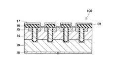
図2に示すように、半導体基板11には、パワーデバイスとして利用可能な縦型のトレンチゲート型IGBTが作り込まれている。半導体基板11には、その裏面側から、第1導電型のコレクタ領域18と、第2導電型のドリフト領域19と、第1導電型のボディ領域14が積層されている。ボディ領域14の表面には第2導電型のエミッタ領域15が形成されている。半導体基板11の表面側からボディ領域14を貫通するトレンチゲート17が設けられている。トレンチゲート17はエミッタ領域15と接している。トレンチゲート17は、ゲート絶縁膜によって覆われたゲート電極を備えている。ゲート電極の表面は、半導体基板11の表面の一部に形成された層間絶縁膜16によって覆われている。 As shown in FIG. 2, a vertical trench gate type IGBT that can be used as a power device is built in the
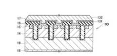
半導体基板11および層間絶縁膜16の表面に接して窒化チタン(TiN)層131が形成されている。さらにその表面にAl層132、Al−Si層133、Ni層134が形成されている。Al層132、Al−Si層133の表面の一部に保護膜としてのポリイミド層140が形成されており、Ni層134の側面と接している。 A titanium nitride (TiN)
TiN層131は、バリア金属層である第1層の一例であり、半導体基板11の表面(エミッタ領域15が形成されている側)に接している。第1層としては、窒化チタン(TiN)の他にも、チタンケイ素(TiSi)等を好適に用いることができる。 The
Al層132は、アルミニウム(Al)を主成分とする第2層の一例であり、TiN層131の表面に接している。第2層としてAl層を用いる場合には、不純物の質量濃度は0.1wt%以下であることが好ましい。第2層は、層間絶縁膜16等の段差を吸収できる厚さであることが好ましく、3〜4μm程度の厚さに形成されることが好ましい。 The
Al−Si層133は、第3層の一例であり、Al層132の表面に接している。第3層としてAl−Si層を用いる場合には、Siの質量濃度は0.1wt%以上かつ2wt%以下であることが好ましい。第3層は、1μm以上の厚さに形成されることが好ましい。 The Al—
第3層としては、Al−Si層の他に、Al−Cu層、Al−Si−Cu層を用いてもよい。第3層としてAl−Cu層を用いる場合、Cuの質量濃度は0.3wt%以上かつ2wt%以下であることが好ましい。第3層としてAl−Si−Cu層を用いる場合、Siの質量濃度は0.1wt%以上かつ2wt%以下であり、Cuの質量濃度は0.3wt%以上かつ2wt%以下であることが好ましい。 As the third layer, an Al—Cu layer or an Al—Si—Cu layer may be used in addition to the Al—Si layer. When an Al—Cu layer is used as the third layer, the mass concentration of Cu is preferably 0.3 wt% or more and 2 wt% or less. When an Al—Si—Cu layer is used as the third layer, the mass concentration of Si is preferably 0.1 wt% or more and 2 wt% or less, and the mass concentration of Cu is preferably 0.3 wt% or more and 2 wt% or less. .
Ni層134は、はんだ接合層である第4層の一例であり、本実施例においては、Al−Si層133の表面に接している。第4層は、第3層の表面に亜鉛置換処理を行った後に形成されたはんだ接合層である。後述するように、本実施例に係るNi層134も、Al−Si層133の表面に亜鉛置換処理を行った後に形成されたものである。第4層としては、はんだと共晶を形成できる材料を用いることができ、本実施例で用いているNiのほか、Cu等を好適に用いることができる。第4層は、3〜10μm程度の厚さに形成されることが好ましい。 The
尚、第4層の表面には、はんだ接合層の酸化を防止する酸化防止層が形成されていてもよい。酸化防止層としては、第4層の表面酸化を防止し、はんだとの濡れ性を確保できる材料を利用でき、金(Au)、銀(Ag)等を好適に用いることができる。 An anti-oxidation layer that prevents oxidation of the solder joint layer may be formed on the surface of the fourth layer. As the antioxidant layer, a material that can prevent surface oxidation of the fourth layer and ensure wettability with solder can be used, and gold (Au), silver (Ag), or the like can be suitably used.
次に、本実施例に係る表面電極の製造方法について説明する。図3に示すように、IGBTが形成された半導体基板11の表面に層間絶縁膜16を形成したシリコン製のウェハ100を用意する。ウェハ100の表面側に、第1層、第2層、第3層、第4層を形成することによって、表面電極を製造する。 Next, the manufacturing method of the surface electrode which concerns on a present Example is demonstrated. As shown in FIG. 3, a
(第1工程)
まず、ウェハ100の表面にスパッタ法によって、第1層としてのTiN層131を形成する。図9は、本実施例に係るTiN層131、Al層132、Al−Si層133を形成するためのスパッタ装置36を概念的に示す図である。スパッタ装置36は、チャンバ34内に、バッキングプレート361と、ターゲット362と、ステージ343とを備えている。スパッタ装置36は、ターゲット362と、ステージ343上に載置するウェハとの間に高電圧を印加することが可能な構成となっている。ターゲット362とステージ343とは、チャンバ34内において対向しており、離間して配置されている。ステージ343には、温度センサが設置されており、ステージ343上に載置されるウェハ100の温度(基板温度)を検知することができる。(First step)
First, a
ウェハ100をステージ343上に載置し、ターゲット362として用いる材料をTiNとし、スパッタを行うことによって、TiN層131をウェハ100の表面に形成することができる。ウェハ100は、層間絶縁膜16が形成されている表面側がターゲット362側となるように、ステージ343上に載置される。チャンバ34内を減圧し、ステージ343に設置された温度センサの検知値に基づき、基板温度が所定の温度となるように制御する。基板温度は、室温(25℃)以上300℃以下の範囲で設定することが好ましい。減圧が完了した後に、チャンバ34内にArガスの導入を開始し、ターゲット362と、ステージ343上に載置するウェハ100との間に高電圧を印加する。これによって、図4に示すように、ウェハ100の表面にTiN層131を形成することができる。 The
(第2工程)
次に、ウェハ100の表面にスパッタ法によって、第2層としてのAl層132を形成する。具体的には、ターゲット362として用いる材料を高純度Alとし、ステージ343に設置された温度センサの検知値に基づき、基板温度が所定の温度となるように制御して、スパッタを行う。基板温度は、室温(25℃)以上300℃以下の範囲で設定することが好ましい。これによって、図5に示すように、TiN層131の表面にAl層132を形成することができる。Al層132は、層間絶縁膜16の段差を覆う程度の厚さに形成されており、Al層132の表面は平坦性が良い状態となっている。(Second step)
Next, an
(第3工程)
次に、スパッタ法によって、第3層としてのAl−Si層133を形成する。具体的には、ターゲット362として用いる材料をAl−Si合金とし、ステージ343に設置された温度センサの検知値に基づき、基板温度が所定の温度となるように制御して、スパッタを行う。基板温度は、室温(25℃)以上300℃以下の範囲で設定することが好ましい。これによって、図6に示すように、Al層132の表面にAl−Si層133を形成することができる。Al層132の表面を平坦性が良い状態とすることによって、Al−Si層133の表面も平坦性が良い状態とすることができる。なお、平坦性の良いAl層132の表面にAl−Si層133を形成するため、Al−Si層133を低温でスパッタしても、Al−Si層133の表面の平坦性を確保することができる。Al−Si層133を低温でスパッタすることができるため、Siノジュールの発生が抑えられる。その結果、表面電極13と半導体基板11とのオーミック接合が確保される。(Third step)
Next, an Al—
なお、Al−Cu層またはAl−Si−Cu層を第3層として形成する場合も、上記と同様の方法を用いることができる。ターゲット362として用いる材料をAl−Cu合金、もしくはAl−Si−Cu合金とし、上記と同様にスパッタ法を行うことによって、Al−Cu層、Al−Si−Cu層を第3層として形成することができる。 Note that a method similar to the above can also be used in the case where an Al—Cu layer or an Al—Si—Cu layer is formed as the third layer. A material used as the
次に、ウェハ100をチャンバ34内から取り出して、図7に示すように、保護層としてのポリイミド層140を形成する。ポリイミド層140は、例えば、ポリアミド酸をウェハ100に塗布した後、アニール処理によって重合することによって形成することができる。 Next, the
(第4工程)
第3層であるAl−Si層133の表面に亜鉛(Zn)置換処理を行う。Zn置換処理では、100g/Lとなるように酸化亜鉛(ZnO)を500g/Lの水酸化ナトリウム(NaOH)溶液に溶解し、ジンケート処理液を調製する。このジンケート処理液中には、ジンケートイオンZnO22−が存在している。このジンケート処理液を用いて、ダブルジンケート処理を行う。(4th process)
Zinc (Zn) substitution treatment is performed on the surface of the Al—
ダブルジンケート処理では、まず、第3工程で形成したAl−Si層133の表面側を、ジンケート処理液に浸漬させる。これによって、Al−Si層133の表面側が溶解し、Zn粒子がAl−Si層133上に析出し、第1次のZn置換膜が形成される。 In the double zincate treatment, first, the surface side of the Al—
次に、硝酸溶液を用いて、第1次のZn置換膜を剥離する。このように、最初に形成した第1次のZn置換膜を一端剥離することによって、Zn置換膜の密着性、緻密性を向上させることができる。 Next, the first Zn substitution film is peeled off using a nitric acid solution. As described above, the first formed Zn-substituted film is peeled off once to improve the adhesion and the denseness of the Zn-substituted film.
第1次のZn置換膜を剥離した後、再び、Al−Si層133の表面側を、ジンケート処理液に浸漬させ、第2次のZn置換膜を形成し、Zn置換処理を終了する。 After peeling off the primary Zn substitution film, the surface side of the Al—
図10は、Al系金属をZn置換処理したときのAl系金属の電位の時間変化について説明する図である。縦軸は、Zn置換処理したときのAl系金属の電位を、Znの自然電位との電位差によって示している。横軸は、Zn置換処理を行う場合の置換時間を示している。図10には、Zn置換処理したAl系金属が第2層の材料であるAlの場合の時間変化と、第3層の材料であるAl−Si、Al−Cu、Al−Si−Cuの場合の時間変化とを図示している。置換時間がゼロの時のAl系金属とZnとの電位差は、そのAl系金属の自然電位とZnの自然電位との電位差を示している。Zn置換処理の時間が経過し、Al系金属の電位がZnの自然電位と同等となると、Al系金属に対してZn置換膜が形成され始める。 FIG. 10 is a diagram for explaining the temporal change in potential of the Al-based metal when the Al-based metal is subjected to Zn substitution treatment. The vertical axis shows the potential of the Al-based metal when the Zn substitution treatment is performed by the potential difference from the natural potential of Zn. The horizontal axis indicates the replacement time when performing the Zn replacement process. FIG. 10 shows a change in time when the Al-based metal subjected to Zn substitution treatment is Al as the material of the second layer, and the case of Al—Si, Al—Cu, and Al—Si—Cu as the materials of the third layer. The change with time is illustrated. The potential difference between the Al-based metal and Zn when the substitution time is zero indicates the potential difference between the natural potential of the Al-based metal and the natural potential of Zn. When the time of the Zn substitution process elapses and the potential of the Al-based metal becomes equal to the natural potential of Zn, a Zn-substituted film starts to be formed on the Al-based metal.
図10より明らかなように、Alの自然電位とZnの自然電位との差は大きい。このため、図10に示すように、Zn置換処理工程において、Alの電位がZnの自然電位と同等となるまでに要する時間は長い。すなわち、Alに対してZn置換処理を行う場合、Zn置換膜が形成され始めるまでに要する時間が長い。この場合、形成されるZn置換膜は、密着性、緻密性に劣った膜となる。 As is clear from FIG. 10, the difference between the natural potential of Al and the natural potential of Zn is large. For this reason, as shown in FIG. 10, it takes a long time for the Al potential to be equal to the natural potential of Zn in the Zn substitution process. That is, when performing Zn substitution treatment on Al, it takes a long time to start forming the Zn substitution film. In this case, the formed Zn-substituted film is a film having poor adhesion and denseness.
一方、Al−Si、Al−Cu、Al−Si−Cuの自然電位は、Alの場合と比較して、Znの自然電位との差が小さい。このため、図10に示すように、Zn置換処理工程において、Al−Si、Al−Cu、Al−Si−Cuの電位がZnの自然電位と同等となるまでに要する時間が短くなる。すなわち、Al−Si、Al−Cu、Al−Si−Cuに対してZn置換処理を行う場合、Zn置換膜が形成され始めるまでに要する時間が短い。このため、形成されるZn置換膜は、Alの場合と比較して、密着性、緻密性に優れた膜となる。本実施例では、第3層であるAl−Si層133の表面にZn置換処理を行うため、密着性、緻密性に優れたZn置換膜を形成することができる。第3層として、Al−Cu層、Al−Si−Cu層を形成する場合においても、同様に、密着性、緻密性に優れたZn置換膜を形成することができる。 On the other hand, the natural potential of Al—Si, Al—Cu, and Al—Si—Cu has a smaller difference from the natural potential of Zn as compared to the case of Al. For this reason, as shown in FIG. 10, in the Zn substitution treatment step, the time required until the potential of Al—Si, Al—Cu, Al—Si—Cu becomes equal to the natural potential of Zn is shortened. That is, in the case where Zn substitution treatment is performed on Al—Si, Al—Cu, and Al—Si—Cu, the time required to start forming the Zn substitution film is short. For this reason, the formed Zn-substituted film is a film having excellent adhesion and denseness as compared with the case of Al. In this embodiment, since the Zn substitution treatment is performed on the surface of the Al—
(第5工程)
Zn置換膜が形成されたAl−Si層133の表面に、図8に示すように、第4層として、Ni層134を無電解めっきによって形成する。Ni層134の無電解めっきは、例えば、還元剤に次亜リン酸ナトリウムを用いるニッケル−リン合金(Ni−P)めっき等によって行うことができる。(5th process)
As shown in FIG. 8, a
尚、第4層の表面に、酸化防止層を形成する場合には、図8に示す状態のウェハ100の表面に酸化防止層を形成する。例えば、酸化防止層としてAu層を形成する場合には、無電解めっき等の方法によって形成することが可能である。 In the case where an antioxidant layer is formed on the surface of the fourth layer, the antioxidant layer is formed on the surface of the
上記の方法によって図2に示す半導体装置10の表面電極13を製造することができる。半導体装置10は、その表面電極13にはんだ層を塗布した後、はんだリフロー工程を行うことによって、半導体モジュール1の表面側の金属板23に接合される。はんだリフロー工程で行われる熱処理によって、Ni層134とはんだ層との合金層が形成されることがある。はんだ層としては、錫(Sn)系、銀(Ag)系、鉛(Pb)系のはんだを好適に用いることができる。 The
上記のとおり、本実施例に係る製造方法においては、Al−Si層またはAl−Cu層またはAl−Si−Cu層よりも平坦性の良い膜を成膜し易いAl層を第2層として用い、バリア金属層である第1層の表面に形成する。このため、第2層の表面の平坦性が良好となる。第2層の表面の平坦性が向上するため、その表面に形成される第3層(即ち、Al−Si層またはAl−Cu層またはAl−Si−Cu層)の表面の平坦性も良好となる。これによって、第3層の表面に形成する、はんだ接合層である第4層を平坦性の良い膜にすることができる。 As described above, in the manufacturing method according to the present embodiment, an Al layer that can easily form a film having better flatness than the Al—Si layer, the Al—Cu layer, or the Al—Si—Cu layer is used as the second layer. And formed on the surface of the first layer which is a barrier metal layer. For this reason, the flatness of the surface of the second layer is improved. Since the flatness of the surface of the second layer is improved, the flatness of the surface of the third layer (that is, the Al—Si layer, the Al—Cu layer, or the Al—Si—Cu layer) formed on the surface is also good. Become. As a result, the fourth layer, which is a solder bonding layer, formed on the surface of the third layer can be a film having good flatness.
また、本実施例のように、第3層として、Al−Si層またはAl−Cu層またはAl−Si−Cu層を形成すると、その後の工程において行うZn置換処理において、密着性と緻密性に優れたZn置換膜を成膜することができる。これによって、はんだ接合層である第4層を平坦性の良い膜にすることができる。 In addition, when an Al—Si layer, an Al—Cu layer, or an Al—Si—Cu layer is formed as the third layer as in this embodiment, adhesion and denseness are improved in the Zn substitution treatment performed in the subsequent process. An excellent Zn-substituted film can be formed. As a result, the fourth layer, which is a solder joint layer, can be made a film having good flatness.
上記のとおり、本実施例によれば、半導体基板と表面電極とのオーミック接合を確保することと、はんだ接合層を平坦性の良い膜とすることとを両立することができる。従来、Zn置換膜を密着性と緻密性に優れた膜として成膜するために、Zn置換処理液に塩化第二鉄などの添加物を加える方法や、Zn置換処理に先立ってAl系金属層表面をエッチングする方法を行う必要があった。本実施例の半導体装置によれば、製造条件によっては、これらの方法が不要となり、製造工程の簡略化、低コスト化にも寄与し得る。 As described above, according to the present embodiment, it is possible to ensure both ohmic bonding between the semiconductor substrate and the surface electrode and to make the solder bonding layer a film having good flatness. Conventionally, in order to form a Zn-substituted film as a film having excellent adhesion and denseness, a method of adding an additive such as ferric chloride to a Zn-substituted treatment liquid, or an Al-based metal layer prior to the Zn-substituted process It was necessary to carry out a method of etching the surface. According to the semiconductor device of this embodiment, these methods are not necessary depending on the manufacturing conditions, which can contribute to simplification of the manufacturing process and cost reduction.
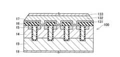
尚、本実施例では、半導体装置の全面に本実施例に係る表面電極が形成されていたが、本実施例に係る表面電極は半導体装置の一部に形成されていてもよい。半導体装置の一部に本実施例に係る表面電極を形成する場合には、比較的発熱量の大きい箇所に形成することが好ましい。このような箇所に、本実施例に係る表面電極が形成されていると、本実施例の表面電極は平坦性の良好なはんだ接合層を有するため、ウェハの反りやはんだ接合層のクラックの抑制に効果的である。例えば、図11に示すように、半導体装置のうち、大電流が流れ、発熱し易いメインセル3の表面電極にのみ本実施例に係る表面電極13を用い、発熱が少ないセンスセル5の表面電極としては従来の表面電極93を用いてもよい。さらに、図12に示すように、メインセル3の表面電極にのみ本実施例に係る表面電極を用いる場合に、第3層の材料がそれぞれ異なる表面電極13a、13b、13cを用いてもよい。例えば、表面電極13aでは第3層がAl−Cu層であり、表面電極13bでは第3層がAl−Si−Cu層であり、表面電極13cでは、第3層がAl−Si層であってもよい。 In this embodiment, the surface electrode according to this embodiment is formed on the entire surface of the semiconductor device. However, the surface electrode according to this embodiment may be formed on a part of the semiconductor device. In the case where the surface electrode according to the present embodiment is formed in a part of the semiconductor device, it is preferable to form the surface electrode in a portion having a relatively large calorific value. If the surface electrode according to the present embodiment is formed in such a place, the surface electrode of the present embodiment has a solder bonding layer with good flatness, so that warpage of the wafer and cracks in the solder bonding layer are suppressed. It is effective. For example, as shown in FIG. 11, in the semiconductor device, the
また、メインセル3の表面電極の一部にのみ本実施例に係る表面電極を用いる場合には、図13や図14に示すように、より発熱によって温度上昇しやすい半導体装置の中央部に本実施例に係る表面電極13を形成することが好ましい。 Further, when the surface electrode according to the present embodiment is used only for a part of the surface electrode of the
以上、本発明の実施例について詳細に説明したが、これらは例示に過ぎず、特許請求の範囲を限定するものではない。特許請求の範囲に記載の技術には、以上に例示した具体例を様々に変形、変更したものが含まれる。 As mentioned above, although the Example of this invention was described in detail, these are only illustrations and do not limit a claim. The technology described in the claims includes various modifications and changes of the specific examples illustrated above.
本明細書または図面に説明した技術要素は、単独であるいは各種の組合せによって技術的有用性を発揮するものであり、出願時請求項記載の組合せに限定されるものではない。また、本明細書または図面に例示した技術は複数目的を同時に達成し得るものであり、そのうちの一つの目的を達成すること自体で技術的有用性を持つものである。 The technical elements described in this specification or the drawings exhibit technical usefulness alone or in various combinations, and are not limited to the combinations described in the claims at the time of filing. In addition, the technology exemplified in this specification or the drawings can achieve a plurality of objects at the same time, and has technical usefulness by achieving one of the objects.
Claims (2)
Translated fromJapaneseその表面電極の少なくとも一部が、半導体基板の表面側に形成された第1層と、第1層の表面側に形成された第2層と、第2層の表面に接する第3層と、第3層の表面側に形成された第4層と、を含んでおり、
前記第1層は、バリア金属層であり、
前記第2層は、Al層であり、
前記第3層は、Al−Si層、またはAl−Cu層、またはAl−Si−Cu層であり、
前記第4層は、はんだ接合層である半導体装置。Comprising a semiconductor substrate and a surface electrode laminated on the surface of the semiconductor substrate;
A first layer formed on the surface side of the semiconductor substrate, at least a part of the surface electrode; a second layer formed on the surface side of the first layer; a third layer in contact with the surface of the second layer; A fourth layer formed on the surface side of the third layer,
The first layer is a barrier metal layer;
The second layer is an Al layer;
The third layer is an Al-Si layer, an Al-Cu layer, or an Al-Si-Cu layer,
The semiconductor device, wherein the fourth layer is a solder joint layer.
半導体基板の表面にバリア金属によって第1層を形成する第1工程と、
前記第1工程の後に、第1層の表面にAlによって第2層を形成する第2工程と、
前記第2工程の後に、前記第2層の表面にAl−SiまたはAl−CuまたはAl−Si−Cuによって第3層を形成する第3工程と、
前記第3工程の後に、前記第3層の表面を亜鉛置換処理する第4工程と、
前記第4工程の後に、前記第3層の表面にはんだ接合層である第4層を無電解めっきによって形成する第5工程とを含む半導体装置の製造方法。A method for manufacturing a semiconductor device comprising a semiconductor substrate and a surface electrode laminated on the surface of the semiconductor substrate,
A first step of forming a first layer with a barrier metal on a surface of a semiconductor substrate;
A second step of forming a second layer with Al on the surface of the first layer after the first step;
After the second step, a third step of forming a third layer on the surface of the second layer with Al-Si, Al-Cu, or Al-Si-Cu;
After the third step, a fourth step of performing zinc substitution on the surface of the third layer;
And a fifth step of forming a fourth layer, which is a solder joint layer, on the surface of the third layer by electroless plating after the fourth step.
Applications Claiming Priority (1)
| Application Number | Priority Date | Filing Date | Title |
|---|---|---|---|
| PCT/JP2009/062448WO2011004469A1 (en) | 2009-07-08 | 2009-07-08 | Semiconductor device and method for manufacturing same |
Publications (2)
| Publication Number | Publication Date |
|---|---|
| JPWO2011004469A1 JPWO2011004469A1 (en) | 2012-12-13 |
| JP5327233B2true JP5327233B2 (en) | 2013-10-30 |
Family
ID=43428908
Family Applications (1)
| Application Number | Title | Priority Date | Filing Date |
|---|---|---|---|
| JP2010547888AExpired - Fee RelatedJP5327233B2 (en) | 2009-07-08 | 2009-07-08 | Semiconductor device and manufacturing method thereof |
Country Status (4)
| Country | Link |
|---|---|
| US (1) | US8426972B2 (en) |
| JP (1) | JP5327233B2 (en) |
| DE (1) | DE112009005044B4 (en) |
| WO (1) | WO2011004469A1 (en) |
Families Citing this family (7)
| Publication number | Priority date | Publication date | Assignee | Title |
|---|---|---|---|---|
| JP5855361B2 (en)* | 2011-05-31 | 2016-02-09 | 三菱電機株式会社 | Semiconductor device |
| JP5684653B2 (en)* | 2011-06-13 | 2015-03-18 | 株式会社Pfu | Image reading device |
| JP2017118060A (en)* | 2015-12-25 | 2017-06-29 | ローム株式会社 | Semiconductor device and semiconductor device manufacturing method |
| DE102016102493B3 (en)* | 2016-02-12 | 2017-07-20 | Infineon Technologies Ag | SEMICONDUCTOR DEVICE WITH A TEMPERATURE SENSOR, TEMPERATURE SENSOR AND METHOD FOR PRODUCING A SEMICONDUCTOR DEVICE WITH A TEMPERATURE SENSOR |
| CN108666287B (en)* | 2017-04-01 | 2020-07-28 | 中芯国际集成电路制造(北京)有限公司 | Pad structure |
| JP6946922B2 (en)* | 2017-10-18 | 2021-10-13 | 株式会社デンソー | Semiconductor device |
| JP7353496B2 (en)* | 2020-07-16 | 2023-09-29 | 三菱電機株式会社 | Power semiconductor equipment |
Citations (5)
| Publication number | Priority date | Publication date | Assignee | Title |
|---|---|---|---|---|
| JPH01318236A (en)* | 1988-06-17 | 1989-12-22 | Sanyo Electric Co Ltd | Semiconductor device and manufacture thereof |
| JP2001284525A (en)* | 2000-03-30 | 2001-10-12 | Denso Corp | Semiconductor chip and semiconductor device |
| JP2002093742A (en)* | 2000-09-18 | 2002-03-29 | National Institute Of Advanced Industrial & Technology | Ohmic electrode structure, method for manufacturing the same, semiconductor device, and method for manufacturing semiconductor device |
| JP2007019412A (en)* | 2005-07-11 | 2007-01-25 | Denso Corp | Semiconductor device and its manufacturing method |
| JP2008501246A (en)* | 2004-05-28 | 2008-01-17 | インターナショナル レクティファイアー コーポレイション | Front contact formation for surface mounting |
Family Cites Families (17)
| Publication number | Priority date | Publication date | Assignee | Title |
|---|---|---|---|---|
| WO1986006878A1 (en)* | 1985-05-10 | 1986-11-20 | Asahi Kasei Kogyo Kabushiki Kaisha | Magneto-electric converter element |
| US4987562A (en)* | 1987-08-28 | 1991-01-22 | Fujitsu Limited | Semiconductor layer structure having an aluminum-silicon alloy layer |
| JP2593965B2 (en)* | 1991-01-29 | 1997-03-26 | 三菱電機株式会社 | Semiconductor device |
| JPH0547764A (en) | 1991-08-07 | 1993-02-26 | Ricoh Co Ltd | Semiconductor device and manufacturing method thereof |
| DE69738324T2 (en)* | 1996-08-27 | 2008-10-09 | Nippon Steel Corp. | METHOD OF MANUFACTURING A SEMICONDUCTOR ASSEMBLY WITH LOW MELTING METAL HEEDS |
| JP3663786B2 (en)* | 1996-10-14 | 2005-06-22 | ヤマハ株式会社 | Semiconductor chip mounting method and structure |
| US6100194A (en)* | 1998-06-22 | 2000-08-08 | Stmicroelectronics, Inc. | Silver metallization by damascene method |
| US6436816B1 (en)* | 1998-07-31 | 2002-08-20 | Industrial Technology Research Institute | Method of electroless plating copper on nitride barrier |
| US6187680B1 (en)* | 1998-10-07 | 2001-02-13 | International Business Machines Corporation | Method/structure for creating aluminum wirebound pad on copper BEOL |
| JP2000114302A (en)* | 1998-10-08 | 2000-04-21 | Fuji Electric Co Ltd | Semiconductor device |
| JP2000252313A (en) | 1999-02-25 | 2000-09-14 | Sony Corp | Formation of plating film and fabrication of semiconductor device |
| US6693350B2 (en) | 1999-11-24 | 2004-02-17 | Denso Corporation | Semiconductor device having radiation structure and method for manufacturing semiconductor device having radiation structure |
| US6703707B1 (en) | 1999-11-24 | 2004-03-09 | Denso Corporation | Semiconductor device having radiation structure |
| TW517334B (en)* | 2000-12-08 | 2003-01-11 | Nec Corp | Method of forming barrier layers for solder bumps |
| DE60238450D1 (en)* | 2002-12-06 | 2011-01-05 | Tamura Seisakusho Kk | PROCEDURE FOR SUPPLYING LOT |
| JP4203724B2 (en) | 2003-03-04 | 2009-01-07 | 上村工業株式会社 | Aluminum oxide film removal solution and surface treatment method of aluminum or aluminum alloy |
| JP2005314738A (en) | 2004-04-28 | 2005-11-10 | Technic Japan Inc | Electroless plating method on aluminum surface, and catalyst for electroless plating |
- 2009
- 2009-07-08JPJP2010547888Apatent/JP5327233B2/ennot_activeExpired - Fee Related
- 2009-07-08WOPCT/JP2009/062448patent/WO2011004469A1/ennot_activeCeased
- 2009-07-08DEDE112009005044.1Tpatent/DE112009005044B4/ennot_activeExpired - Fee Related
- 2012
- 2012-01-06USUS13/345,165patent/US8426972B2/ennot_activeExpired - Fee Related
Patent Citations (5)
| Publication number | Priority date | Publication date | Assignee | Title |
|---|---|---|---|---|
| JPH01318236A (en)* | 1988-06-17 | 1989-12-22 | Sanyo Electric Co Ltd | Semiconductor device and manufacture thereof |
| JP2001284525A (en)* | 2000-03-30 | 2001-10-12 | Denso Corp | Semiconductor chip and semiconductor device |
| JP2002093742A (en)* | 2000-09-18 | 2002-03-29 | National Institute Of Advanced Industrial & Technology | Ohmic electrode structure, method for manufacturing the same, semiconductor device, and method for manufacturing semiconductor device |
| JP2008501246A (en)* | 2004-05-28 | 2008-01-17 | インターナショナル レクティファイアー コーポレイション | Front contact formation for surface mounting |
| JP2007019412A (en)* | 2005-07-11 | 2007-01-25 | Denso Corp | Semiconductor device and its manufacturing method |
Also Published As
| Publication number | Publication date |
|---|---|
| US20120104612A1 (en) | 2012-05-03 |
| DE112009005044B4 (en) | 2014-04-30 |
| US8426972B2 (en) | 2013-04-23 |
| WO2011004469A1 (en) | 2011-01-13 |
| DE112009005044T5 (en) | 2012-06-21 |
| JPWO2011004469A1 (en) | 2012-12-13 |
Similar Documents
| Publication | Publication Date | Title |
|---|---|---|
| JP5549118B2 (en) | Manufacturing method of semiconductor device | |
| JP5327233B2 (en) | Semiconductor device and manufacturing method thereof | |
| JP5160201B2 (en) | Solder material and manufacturing method thereof, joined body and manufacturing method thereof, power semiconductor module and manufacturing method thereof | |
| JP6432466B2 (en) | Bonded body, power module substrate with heat sink, heat sink, method for manufacturing bonded body, method for manufacturing power module substrate with heat sink, and method for manufacturing heat sink | |
| JP6432465B2 (en) | Bonded body, power module substrate with heat sink, heat sink, method for manufacturing bonded body, method for manufacturing power module substrate with heat sink, and method for manufacturing heat sink | |
| JP6651271B2 (en) | Semiconductor device and manufacturing method thereof | |
| JP5214936B2 (en) | Semiconductor device | |
| JP6191587B2 (en) | Semiconductor device | |
| TWI582851B (en) | Electrode structure and semiconductor device | |
| JP5725061B2 (en) | Power module substrate and power module substrate with heat sink | |
| JP2008198706A (en) | Circuit board, method for manufacturing the same, and semiconductor module using the same | |
| JP2009129983A (en) | CONNECTED BODY AND ITS MANUFACTURING METHOD, POWER SEMICONDUCTOR MODULE AND ITS MANUFACTURING METHOD | |
| JP4344560B2 (en) | Semiconductor chip and semiconductor device using the same | |
| JP5494559B2 (en) | Semiconductor device and manufacturing method thereof | |
| JP2016042528A (en) | Bonded body, power module substrate, power module substrate with heat sink, bonded body manufacturing method, power module substrate manufacturing method, and heat module power module substrate manufacturing method | |
| JP2018125354A (en) | Semiconductor device | |
| US10461050B2 (en) | Bonding pad structure of a semiconductor device | |
| JP6918902B2 (en) | Manufacturing method of semiconductor devices | |
| JP2021072409A (en) | Semiconductor device | |
| JPH11214446A (en) | Electronic component manufacturing method | |
| JP5434087B2 (en) | Semiconductor device and method of soldering the semiconductor device | |
| JP2018139276A (en) | Silicon carbide semiconductor device and manufacturing method thereof |
Legal Events
| Date | Code | Title | Description |
|---|---|---|---|
| TRDD | Decision of grant or rejection written | ||
| A01 | Written decision to grant a patent or to grant a registration (utility model) | Free format text:JAPANESE INTERMEDIATE CODE: A01 Effective date:20130625 | |
| A61 | First payment of annual fees (during grant procedure) | Free format text:JAPANESE INTERMEDIATE CODE: A61 Effective date:20130708 | |
| R151 | Written notification of patent or utility model registration | Ref document number:5327233 Country of ref document:JP Free format text:JAPANESE INTERMEDIATE CODE: R151 | |
| S111 | Request for change of ownership or part of ownership | Free format text:JAPANESE INTERMEDIATE CODE: R313113 | |
| R350 | Written notification of registration of transfer | Free format text:JAPANESE INTERMEDIATE CODE: R350 | |
| R250 | Receipt of annual fees | Free format text:JAPANESE INTERMEDIATE CODE: R250 | |
| R250 | Receipt of annual fees | Free format text:JAPANESE INTERMEDIATE CODE: R250 | |
| R250 | Receipt of annual fees | Free format text:JAPANESE INTERMEDIATE CODE: R250 | |
| LAPS | Cancellation because of no payment of annual fees |