JP5320746B2 - Thin film transistor - Google Patents
Thin film transistorDownload PDFInfo
- Publication number
- JP5320746B2 JP5320746B2JP2008007887AJP2008007887AJP5320746B2JP 5320746 B2JP5320746 B2JP 5320746B2JP 2008007887 AJP2008007887 AJP 2008007887AJP 2008007887 AJP2008007887 AJP 2008007887AJP 5320746 B2JP5320746 B2JP 5320746B2
- Authority
- JP
- Japan
- Prior art keywords
- gate insulating
- insulating layer
- oxide
- thin film
- film transistor
- Prior art date
- Legal status (The legal status is an assumption and is not a legal conclusion. Google has not performed a legal analysis and makes no representation as to the accuracy of the status listed.)
- Expired - Fee Related
Links
Images


Classifications
- H—ELECTRICITY
- H10—SEMICONDUCTOR DEVICES; ELECTRIC SOLID-STATE DEVICES NOT OTHERWISE PROVIDED FOR
- H10D—INORGANIC ELECTRIC SEMICONDUCTOR DEVICES
- H10D30/00—Field-effect transistors [FET]
- H10D30/60—Insulated-gate field-effect transistors [IGFET]
- H10D30/67—Thin-film transistors [TFT]
- H10D30/674—Thin-film transistors [TFT] characterised by the active materials
- H10D30/6755—Oxide semiconductors, e.g. zinc oxide, copper aluminium oxide or cadmium stannate
- H—ELECTRICITY
- H10—SEMICONDUCTOR DEVICES; ELECTRIC SOLID-STATE DEVICES NOT OTHERWISE PROVIDED FOR
- H10D—INORGANIC ELECTRIC SEMICONDUCTOR DEVICES
- H10D30/00—Field-effect transistors [FET]
- H10D30/60—Insulated-gate field-effect transistors [IGFET]
- H10D30/67—Thin-film transistors [TFT]
- H10D30/6704—Thin-film transistors [TFT] having supplementary regions or layers in the thin films or in the insulated bulk substrates for controlling properties of the device
- H10D30/6706—Thin-film transistors [TFT] having supplementary regions or layers in the thin films or in the insulated bulk substrates for controlling properties of the device for preventing leakage current
- H—ELECTRICITY
- H10—SEMICONDUCTOR DEVICES; ELECTRIC SOLID-STATE DEVICES NOT OTHERWISE PROVIDED FOR
- H10D—INORGANIC ELECTRIC SEMICONDUCTOR DEVICES
- H10D30/00—Field-effect transistors [FET]
- H10D30/60—Insulated-gate field-effect transistors [IGFET]
- H10D30/67—Thin-film transistors [TFT]
- H10D30/6729—Thin-film transistors [TFT] characterised by the electrodes
- H10D30/6737—Thin-film transistors [TFT] characterised by the electrodes characterised by the electrode materials
- H10D30/6739—Conductor-insulator-semiconductor electrodes
Landscapes
- Thin Film Transistor (AREA)
- Formation Of Insulating Films (AREA)
Description
Translated fromJapanese本発明は、各種画像表示装置の駆動素子や各種論理回路の論理素子等に用いることができる薄膜トランジスタに関する。The present invention relates to a thin film transistor that can be used for driving elements of various image display devices, logic elements of various logic circuits, and the like.
現在、一般的な平面薄型画像表示装置(Flat Panel Display;FPD)は、半導体に非晶質シリコンや多結晶シリコンを用いた電界効果型薄膜トランジスタにより駆動するアクティブマトリックスタイプのものが主流となっている。At present, a general flat panel display (FPD) is mainly an active matrix type driven by a field effect thin film transistor using amorphous silicon or polycrystalline silicon as a semiconductor. .
一方、FPDのさらなる薄型化及び軽量化、耐衝撃性や可撓性の向上を目的に、ガラス基板の代わりにプラスチック基板を用いる試みが近年なされている。On the other hand, attempts have been made in recent years to use a plastic substrate instead of a glass substrate for the purpose of further reducing the thickness and weight of the FPD, and improving impact resistance and flexibility.
しかしながら、上述のシリコンを半導体に用いた薄膜トランジスタの製造は、高温の熱工程を要し、耐熱性の低いプラスチック基板に適用するのは困難である。However, the manufacture of the above-described thin film transistor using silicon as a semiconductor requires a high-temperature heat process and is difficult to apply to a plastic substrate with low heat resistance.
そこで、低温形成が可能な酸化物を半導体に用いた電界効果型薄膜トランジスタの開発が活発に行われてきている(特許文献1)。Therefore, development of a field effect thin film transistor using an oxide that can be formed at a low temperature as a semiconductor has been actively performed (Patent Document 1).
そして、上述の酸化物半導体を用いた電界効果型薄膜トランジスタのゲート絶縁層としては、例えば酸化シリコン、窒化シリコン、酸化アルミニウム、酸化イットリウム等の無機材料が用いられている。As the gate insulating layer of the field effect thin film transistor using the above-described oxide semiconductor, an inorganic material such as silicon oxide, silicon nitride, aluminum oxide, yttrium oxide, or the like is used.
しかしながら、このようなゲート絶縁層は、基板との密着性が低いため、基板からゲート絶縁層が剥がれやすく、トランジスタ特性が良好な薄膜トランジスタが得られないという問題があった。However, since such a gate insulating layer has low adhesion to the substrate, there is a problem in that the gate insulating layer is easily peeled off from the substrate and a thin film transistor with favorable transistor characteristics cannot be obtained.
そこで本発明では、上記のような問題を解決するため、基板とゲート絶縁層の密着性が高く、トランジスタ特性が良好な薄膜トランジスタを提供することを課題とする。In view of the above, an object of the present invention is to provide a thin film transistor in which the adhesion between the substrate and the gate insulating layer is high and the transistor characteristics are favorable in order to solve the above-described problems.
本発明は上記目的を達成するためになされたものであり、請求項1に記載の発明は、ポリメチルメタクリレート、ポリアクリレート、ポリカーボネート、ポリスチレン、ポリエチレンサルファイド、ポリエーテルスルホン、ポリオレフィン、ポリエチレンテレフタレート、ポリエチレンナフタレート、シクロオレフィンポリマー、ポリエーテルサルフェン、トリアセチルセルロース、ポリビニルフルオライドフィルム、エチレン-テトラフルオロエチレン共重合樹脂、耐候性ポリエチレンテレフタレート、耐候性ポリプロピレン、ガラス繊維強化アクリル樹脂フィルム、ガラス繊維強化ポリカーボネート、透明性ポリイミド、フッ素系樹脂、環状ポリオレフィン系樹脂のいずれか一種以上の材料からなるプラスチック基板上に少なくとも、ゲート電極、ゲート絶縁層、酸化物を含む半導体層が順次積層され、前記半導体層上にソース電極とドレイン電極が設けられた薄膜トランジスタであって、前記ゲート絶縁層が前記絶縁基板に接する下部層と前記下部層上に設けられた少なくとも一層以上の上部層からなり、且つ前記下部層はInZnGaO4を含む酸化物であることを特徴とする薄膜トランジスタである。The present invention has been made to achieve the above object, and the invention according to
ゲート絶縁層の絶縁基板に接する下部層が、InZnGaO4を含む酸化物であることにより、絶縁基板とゲート絶縁層の密着性が向上する。When the lower layer of the gate insulating layer in contact with the insulating substrate is an oxide containingInZnGaO4 , adhesion between the insulating substrate and the gate insulating layer is improved.
請求項2に記載の発明はポリメチルメタクリレート、ポリアクリレート、ポリカーボネート、ポリスチレン、ポリエチレンサルファイド、ポリエーテルスルホン、ポリオレフィン、ポリエチレンテレフタレート、ポリエチレンナフタレート、シクロオレフィンポリマー、ポリエーテルサルフェン、トリアセチルセルロース、ポリビニルフルオライドフィルム、エチレン-テトラフルオロエチレン共重合樹脂、耐候性ポリエチレンテレフタレート、耐候性ポリプロピレン、ガラス繊維強化アクリル樹脂フィルム、ガラス繊維強化ポリカーボネート、透明性ポリイミド、フッ素系樹脂、環状ポリオレフィン系樹脂のいずれか一種以上の材料からなるプラスチック基板上に少なくとも、ゲート電極、ゲート絶縁層が順次積層され、前記ゲート絶縁層上にソース電極とドレイン電極が設けられ、少なくとも前記ソース電極と前記ドレイン電極との間の前記ゲート絶縁層上に酸化物を含む半導体層が設けられた薄膜トランジスタであって、前記ゲート絶縁層が前記絶縁基板に接する下部層と前記下部層上に設けられた少なくとも一層以上の上部層からなり、且つ前記下部層はInZnGaO4を含む酸化物であることを特徴とする薄膜トランジスタである。The invention according to
ゲート絶縁層の絶縁基板に接する下部層が、InZnGaO4を含む酸化物であることにより、絶縁基板とゲート絶縁層の密着性が向上する。When the lower layer of the gate insulating layer in contact with the insulating substrate is an oxide containingInZnGaO4 , adhesion between the insulating substrate and the gate insulating layer is improved.
請求項3に記載の発明は、前記上部層の少なくとも一層が、酸化シリコン、窒化シリコン、シリコンオキシナイトライド、酸化アルミニウム、酸化タンタル、酸化イットリウム、酸化ハフニウム、ハフニウムアルミネート、酸化ジルコニア、酸化チタンのいずれか1種の化合物を含むことを特徴とする請求項1または2に記載の薄膜トランジスタである。According to a third aspect of the present invention, at least one of the upper layers is made of silicon oxide, silicon nitride, silicon oxynitride, aluminum oxide, tantalum oxide, yttrium oxide, hafnium oxide, hafnium aluminate, zirconia oxide, or titanium oxide. The thin film transistor according to
上部層の少なくとも一層が、酸化シリコン、窒化シリコン、シリコンオキシナイトライド、酸化アルミニウム、酸化タンタル、酸化イットリウム、酸化ハフニウム、ハフニウムアルミネート、酸化ジルコニア、酸化チタンのいずれか1種の化合物を含むことで、十分な絶縁性を呈し、ゲートリーク電流が抑制される。At least one of the upper layers contains any one compound of silicon oxide, silicon nitride, silicon oxynitride, aluminum oxide, tantalum oxide, yttrium oxide, hafnium oxide, hafnium aluminate, zirconia oxide, and titanium oxide. It exhibits sufficient insulation and suppresses gate leakage current.
請求項4に記載の発明は、前記上部層の少なくとも一層が、ポリアクリレート、ポリビニルアルコール、ポリスチレン、ポリイミド、ポリエステル、エポキシ、ポリビニルフェノール、ポリビニルアルコールのいずれか1種の化合物を含むことを特徴とする請求項1または2に記載の薄膜トランジスタである。The invention according to
上部層の少なくとも一層が、ポリアクリレート、ポリビニルアルコール、ポリスチレン、ポリイミド、ポリエステル、エポキシ、ポリビニルフェノール、ポリビニルアルコールのいずれか1種の化合物を含むことで、十分な絶縁性を呈し、ゲートリーク電流が抑制される。When at least one of the upper layers contains any one compound of polyacrylate, polyvinyl alcohol, polystyrene, polyimide, polyester, epoxy, polyvinyl phenol, and polyvinyl alcohol, it exhibits sufficient insulation and suppresses gate leakage current. Is done.
請求項5に記載の発明は、前記下部層の膜厚が、ゲート絶縁層全体の膜厚の2/3以下であることを特徴とする請求項1乃至4のいずれかに記載の薄膜トランジスタである。The invention according to
ゲート絶縁層の下部層の膜厚が、ゲート絶縁層全体の膜厚の2/3以下であることでゲート絶縁層全体として十分な絶縁性を呈し、ゲートリーク電流が抑制される。また、下部層に用いる材料は上部層に用いる材料と比較して高価であるため、膜厚を2/3以下に抑えることで生産時のコストダウンにつながる。When the film thickness of the lower layer of the gate insulating layer is 2/3 or less of the film thickness of the entire gate insulating layer, sufficient insulation is exhibited as the entire gate insulating layer, and gate leakage current is suppressed. In addition, since the material used for the lower layer is more expensive than the material used for the upper layer, suppressing the film thickness to 2/3 or less leads to cost reduction during production.
請求項6に記載の発明は、前記下部層の膜厚が、2nm以上200nm以下であることを特徴とする請求項1乃至4のいずれかに記載の薄膜トランジスタである。A sixth aspect of the present invention is the thin film transistor according to any one of the first to fourth aspects, wherein the lower layer has a thickness of 2 nm to 200 nm.
ゲート絶縁層の下部層の膜厚が2nm以上であることを特徴とすることで、膜が島状に形成されることを防止し、基板全体を完全に被覆した膜とすることができる。またゲート絶縁層の下部層の膜厚が200nm以下であることを特徴とすることで、膜厚の増大に伴う膜の応力の増大による、剥がれが防止された膜を形成することができる。Since the thickness of the lower layer of the gate insulating layer is 2 nm or more, the film can be prevented from being formed in an island shape, and a film that completely covers the entire substrate can be obtained. In addition, since the thickness of the lower layer of the gate insulating layer is 200 nm or less, a film in which peeling due to an increase in stress of the film accompanying an increase in the thickness can be formed.
請求項7に記載の発明は、前記下部層の抵抗率が1010Ω・cm以上であることを特徴とする請求項1乃至6のいずれかに記載の薄膜トランジスタである。The invention according to claim 7 is the thin film transistor according to any one of
ゲート絶縁層の下部層の抵抗率が1010Ω・cm以上であることでゲート絶縁層全体として十分な絶縁性を呈し,ゲートリーク電流が抑制される。When the resistivity of the lower layer of the gate insulating layer is 1010 Ω · cm or more, the gate insulating layer as a whole exhibits sufficient insulation, and gate leakage current is suppressed.
本発明によれば、ゲート絶縁層の絶縁基板に接する下部層がIn、Zn、Gaのいずれか1種の元素を含む酸化物であることにより、基板へのゲート絶縁層の密着性が向上し、移動度やON/OFF比が大きく、ゲートリーク電流が小さい、良好なトランジスタ特性を有する薄膜トランジスタを提供することができた。According to the present invention, the adhesion of the gate insulating layer to the substrate is improved because the lower layer of the gate insulating layer in contact with the insulating substrate is an oxide containing any one element of In, Zn, and Ga. Thus, it was possible to provide a thin film transistor having a good mobility and a high ON / OFF ratio, a small gate leakage current, and good transistor characteristics.
以下、本発明の実施の形態を、図面を用いて詳細に説明するが本発明はこれらに限定されるものではない。Hereinafter, embodiments of the present invention will be described in detail with reference to the drawings, but the present invention is not limited thereto.
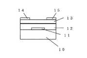
図1に本発明の薄膜トランジスタの一例を示す。絶縁基板10上に、ゲート電極11、ゲート絶縁層12、半導体層13、ソース電極14、ドレイン電極15が形成されている。そしてゲート絶縁層12が下部ゲート絶縁層12aと上部ゲート絶縁層12bからなり、絶縁基板に接する下部ゲート絶縁層12aがIn、Zn、Gaのいずれか1種の元素を含む酸化物であることを特徴とする。FIG. 1 shows an example of a thin film transistor of the present invention. A gate electrode 11, a gate insulating layer 12, a semiconductor layer 13, a
図2に本発明の薄膜トランジスタの他の例を示す。絶縁基板10上に、ゲート電極11、ゲート絶縁層12、ソース電極14、ドレイン電極15、ソース電極14とドレイン電極15間に半導体層13が形成されている。そしてゲート絶縁層12が下部ゲート絶縁層12aと上部ゲート絶縁層12bからなり、絶縁基板に接する下部ゲート絶縁層12aがIn、Zn、Gaのいずれか1種の元素を含む酸化物であることを特徴とする。FIG. 2 shows another example of the thin film transistor of the present invention. A gate electrode 11, a gate insulating layer 12, a
絶縁基板10には、例えばガラスやプラスチック基板を用いることができる。プラスチック基板としては、例えば、ポリメチルメタクリレート、ポリアクリレート、ポリカーボネート、ポリスチレン、ポリエチレンサルファイド、ポリエーテルスルホン、ポリオレフィン、ポリエチレンテレフタレート、ポリエチレンナフタレート、シクロオレフィンポリマー、ポリエーテルサルフェン、トリアセチルセルロース、ポリビニルフルオライドフィルム、エチレン-テトラフルオロエチレン共重合樹脂、耐候性ポリエチレンテレフタレート、耐候性ポリプロピレン、ガラス繊維強化アクリル樹脂フィルム、ガラス繊維強化ポリカーボネート、透明性ポリイミド、フッ素系樹脂、環状ポリオレフィン系樹脂等を使用することができる。これらの基板は単独で使用することもでき、二種以上を積層した複合基板を使用することもできる。As the
プラスチック基板等の可撓性基板であれば、薄型、軽量、フレキシブルな薄膜トランジスタを得ることができ好ましい。また、製造工程に乾燥工程等の熱処理を含む場合には、熱安定性の高い石英などのガラス基板の他、プラスチック基板ではPESやPENが好ましい。A flexible substrate such as a plastic substrate is preferable because a thin, light, and flexible thin film transistor can be obtained. When the manufacturing process includes a heat treatment such as a drying process, PES or PEN is preferable for a plastic substrate in addition to a glass substrate such as quartz having high thermal stability.
本発明のゲート電極11、ソース電極14及びドレイン電極15には、酸化インジウム(In2O3)、酸化スズ(SnO2)、酸化亜鉛(ZnO)、酸化カドミウム(CdO)、酸化インジウムカドミウム(CdIn2O4)、酸化カドミウムスズ(Cd2SnO4)、酸化亜鉛スズ(Zn2SnO4)、酸化インジウム亜鉛(In−Zn−O)等の酸化物材料が好適に用いられる。またこの酸化物材料に不純物をドープすることも導電率を上げるために好ましい。例えば、酸化インジウムにスズやモリブデン、チタンをドープしたもの、酸化スズにアンチモンやフッ素をドープしたもの、酸化亜鉛にインジウム、アルミニウム、ガリウムをドープしたものなどである。この中では特に酸化インジウムにスズをドープした酸化インジウムスズ(通称ITO)が低い抵抗率のために特に好適に用いられる。またAu、Ag、Cu、Cr、Al、Mg、Liなどの低抵抗金属材料も好適に用いられる。また導電性酸化物材料と低抵抗金属材料を複数積層したものも使用できる。この場合、金属材料の酸化や経時劣化を防ぐために導電性酸化物薄膜/金属薄膜/導電性酸化物薄膜の順に積層した3層構造が特に好適に用いられる。またPEDOT (ポリエチレンジオキシチオフェン)等の有機導電性材料も好適に用いることができる。ゲート電極、ソース電極及びドレイン電極は全て同じ材料であっても構わないし、また全て違う材料であっても構わない。しかし、工程数を減らすためにソース電極とドレイン電極は同一の材料であることがより望ましい。これらの電極は、真空蒸着法、イオンプレーティング法、スパッタ法、レーザーアブレーション法、プラズマCVD(ChemicalVapor Deposition)、光CVD法、ホットワイヤーCVD法、またはスクリーン印刷、凸版印刷、インクジェット法等で形成することができるが、これらに限定されるものではない。The gate electrode 11, the
ゲート絶縁層12は下部ゲート絶縁層12aと上部ゲート絶縁層12bで構成される。ゲート絶縁層12の厚さは50nm〜2μmとすることが好ましい。本発明の絶縁基板10と接する下部ゲート絶縁層12aに用いる材料は、In、Zn、Gaのいずれか1種の元素を含む酸化物である。例えば、酸化インジウムガリウム亜鉛(InGaZnO4)、酸化亜鉛(ZnO)、酸化ガリウム(Ga2O3)、酸化ガリウム亜鉛(ZnGa2O4)等が挙げられるがこれらに限定されるものではない。これらの材料の構造は単結晶、多結晶、微結晶、結晶/アモルファスの混晶、ナノ結晶散在アモルファス、アモルファスのいずれであってもよい。上記、下部ゲート絶縁層12aの抵抗値は1010Ω・cm以上が好ましく、より好ましくは1012Ω・cm以上である。抵抗値が1010Ω・cmより小さいと、ゲート絶縁層全体として十分な絶縁性を呈することができず、ゲートリーク電流が増大し、良好な素子特性を得ることができない場合がある。The gate insulating layer 12 includes a lower gate insulating layer 12a and an upper gate insulating layer 12b. The thickness of the gate insulating layer 12 is preferably 50 nm to 2 μm. The material used for the lower gate insulating layer 12a in contact with the insulating
上述の酸化物材料は酸素欠損が生じやすいため、導電性材料や半導体材料として用いられることもあるが、成膜条件を制御し、膜の組成を化学両論比に近づけることで抵抗値を1010Ω・cm以上とすることができる。Since the oxide material described above prone to oxygen deficiency, also be used as a conductive material or a semiconductor material, by controlling the deposition conditions, 10 the resistance value be close to stoichiometric ratio composition of the film10 It can be set to Ω · cm or more.
また下部ゲート絶縁層12aの膜厚が、ゲート絶縁層全体の膜厚の2/3以下であることが良好な素子特性を得るために望ましい。下部ゲート絶縁層12aの膜厚が、ゲート絶縁層全体の膜厚の2/3より大きいと、ゲート絶縁層全体として十分な絶縁性を呈することができず、ゲートリーク電流が増大し、良好な素子特性を得ることができない場合がある。In addition, it is desirable that the thickness of the lower gate insulating layer 12a be 2/3 or less of the total thickness of the gate insulating layer in order to obtain good device characteristics. If the thickness of the lower gate insulating layer 12a is larger than 2/3 of the total thickness of the gate insulating layer, sufficient insulation cannot be obtained as the entire gate insulating layer, and the gate leakage current increases, which is favorable. In some cases, device characteristics cannot be obtained.
また下部ゲート絶縁層12aの膜厚は、2nm以上200nm以下が好ましい。2nmより薄いと基板全体を完全に被覆することができない場合が生じやすく、200nmより厚いと膜の応力が大きくなり剥離が生じやすい。The thickness of the lower gate insulating layer 12a is preferably 2 nm or more and 200 nm or less. If the thickness is less than 2 nm, the entire substrate may not be completely covered. If the thickness is more than 200 nm, the stress of the film increases and peeling tends to occur.
下部ゲート絶縁層12aはスパッタ法、パルスレーザー堆積法、真空蒸着法、CVD法、ゾルゲル法などの方法を用いて形成されるが、好ましくはスパッタ法、パルスレーザー堆積法、真空蒸着法、CVD法である。スパッタ法ではRFマグネトロンスパッタ法、DCスパッタ法、真空蒸着では加熱蒸着、電子ビーム蒸着、イオンプレーティング法、CVD法ではホットワイヤーCVD法、プラズマCVD法などが挙げられるがこれらに限定されるものではない。The lower gate insulating layer 12a is formed by using a sputtering method, a pulse laser deposition method, a vacuum evaporation method, a CVD method, a sol-gel method, etc., but preferably a sputtering method, a pulse laser deposition method, a vacuum evaporation method, a CVD method. It is. Examples of sputtering include RF magnetron sputtering, DC sputtering, vacuum deposition includes heating deposition, electron beam deposition, ion plating, and CVD includes hot wire CVD and plasma CVD. Absent.
本発明で用いられる薄膜トランジスタの上部ゲート絶縁層12bは単層とすることもでき、複数の層を積層することもできる。上部ゲート絶縁層12bの材料はゲートリーク電流を抑制するための十分な絶縁性を有していれば特に制限はないが、抵抗率が1011Ω・cm以上の材料が好ましく、さらには1014Ω・cm以上であることが好ましい。The upper gate insulating layer 12b of the thin film transistor used in the present invention can be a single layer or a plurality of layers can be stacked. The material of the upper gate insulating layer 12b is not particularly limited as long as it has sufficient insulating properties for suppressing the gate leakage current, but a material having a resistivity of 1011 Ω · cm or more is preferable, and more preferably 1014. It is preferable that it is Ω · cm or more.
例えば無機材料としては、酸化シリコン、窒化シリコン、シリコンオキシナイトライド、酸化アルミニウム、酸化タンタル、酸化イットリウム、酸化ハフニウム、ハフニウムアルミネート、酸化ジルコニア、酸化チタン等を挙げることができ、これらの材料を用いることでゲートリーク電流を抑制するために十分な絶縁性を得ることができる。Examples of inorganic materials include silicon oxide, silicon nitride, silicon oxynitride, aluminum oxide, tantalum oxide, yttrium oxide, hafnium oxide, hafnium aluminate, zirconia oxide, and titanium oxide, and these materials are used. Thus, sufficient insulation can be obtained to suppress the gate leakage current.
また有機材料としては、PMMA (ポリメチルメタクリレート)等のポリアクリレート、PVA(ポリビニルアルコール)、PS(ポリスチレン)、透明性ポリイミド、ポリエステル、エポキシ、ポリビニルフェノール、ポリビニルアルコール等が挙げられ、これらの材料を用いることで、ゲートリーク電流を抑制するために十分な絶縁性を得ることができる。Examples of the organic material include polyacrylates such as PMMA (polymethyl methacrylate), PVA (polyvinyl alcohol), PS (polystyrene), transparent polyimide, polyester, epoxy, polyvinylphenol, polyvinyl alcohol, and the like. By using it, sufficient insulation can be obtained to suppress the gate leakage current.
上部ゲート絶縁層12bは真空蒸着法、イオンプレーティング法、スパッタ法、レーザーアブレーション法、プラズマCVD、光CVD法、ホットワイヤーCVD法、スピンコート、ディップコート、スクリーン印刷などの方法を用いて形成される。これらの上部ゲート絶縁層12bは膜の成長方向に向けて組成を傾斜したものもまた好適に用いることができる。The upper gate insulating layer 12b is formed using a method such as vacuum deposition, ion plating, sputtering, laser ablation, plasma CVD, photo CVD, hot wire CVD, spin coating, dip coating, or screen printing. The As these upper gate insulating layers 12b, those whose composition is inclined toward the growth direction of the film can also be suitably used.
本発明で用いられる薄膜トランジスタの半導体層13としては、例えば、亜鉛、インジウム、スズ、タングステン、マグネシウム、ガリウムのうち一種類以上の元素を含む酸化物が挙げられる。酸化亜鉛、酸化インジウム、酸化インジウム亜鉛、酸化スズ、酸化タングステン、酸化亜鉛ガリウムインジウム(In―Ga―Zn―O)等公知の材料が挙げられるがこれらに限定されるものではない。これらの材料の構造は単結晶、多結晶、微結晶、結晶/アモルファスの混晶、ナノ結晶散在アモルファス、アモルファスのいずれであってもかまわない。半導体層の膜厚は少なくとも10nm以上が望ましい。10nmより小さいと膜が島状に形成され、膜中に半導体が形成されていない部分が生じやすい。Examples of the semiconductor layer 13 of the thin film transistor used in the present invention include an oxide containing one or more elements of zinc, indium, tin, tungsten, magnesium, and gallium. Well-known materials such as zinc oxide, indium oxide, indium zinc oxide, tin oxide, tungsten oxide, and zinc gallium indium oxide (In—Ga—Zn—O) may be used, but the material is not limited to these. The structure of these materials may be single crystal, polycrystal, microcrystal, crystal / amorphous mixed crystal, nanocrystal scattered amorphous, or amorphous. The thickness of the semiconductor layer is desirably at least 10 nm. If the thickness is smaller than 10 nm, the film is formed in an island shape, and a portion in which no semiconductor is formed tends to occur in the film.
酸化物半導体層はスパッタ法、パルスレーザー堆積法、真空蒸着法、CVD法、ゾルゲル法などの方法を用いて形成されるが、好ましくはスパッタ法、パルスレーザー堆積法、真空蒸着法、CVD法である。スパッタ法ではRFマグネトロンスパッタ法、DCスパッタ法、真空蒸着では加熱蒸着、電子ビーム蒸着、イオンプレーティング法、CVD法ではホットワイヤーCVD法、プラズマCVD法などが挙げられるがこれらに限定されるものではない。The oxide semiconductor layer is formed using a sputtering method, a pulse laser deposition method, a vacuum evaporation method, a CVD method, a sol-gel method, or the like, but preferably a sputtering method, a pulse laser deposition method, a vacuum evaporation method, or a CVD method. is there. Examples of sputtering include RF magnetron sputtering, DC sputtering, vacuum deposition includes heating deposition, electron beam deposition, ion plating, and CVD includes hot wire CVD and plasma CVD. Absent.
酸化物は、その構成金属元素の比は同じでも全体に対する酸素の比を変えることで、異なる電気特性(抵抗値)を持つ薄膜を形成することが可能である。例えばスパッタ法を用いる場合、同じターゲットを用いても、成膜時の酸素分圧を変えることで電気特性の異なる膜を形成することができる。よって半導体層に酸化物を用いる場合には、電気特性の異なる下部ゲート絶縁層12aと半導体層13を、同じ材料を用いて形成することが可能であり、生産時のコストダウンにつながるため、このような方法を用いることが望ましい。An oxide can form thin films having different electrical characteristics (resistance values) by changing the ratio of oxygen to the whole even if the ratio of constituent metal elements is the same. For example, when the sputtering method is used, even if the same target is used, films having different electrical characteristics can be formed by changing the oxygen partial pressure during film formation. Therefore, when an oxide is used for the semiconductor layer, the lower gate insulating layer 12a and the semiconductor layer 13 having different electrical characteristics can be formed using the same material, which leads to cost reduction during production. It is desirable to use such a method.
(実施例1)
絶縁基板10としてPEN基材(帝人デュポン社製Q65 厚さ125μm)上に、DCマグネトロンスパッタ装置を用いてITOを100nm成膜し、フォトリソグラフィー法を用いてゲート電極11を形成した。次にRFマグネトロンスパッタ法を用いてIn―Ga―Zn―O系酸化物からなる絶縁基板10と接する下部ゲート絶縁層12a(膜厚100nm)、SiONからなる上部ゲート絶縁層12b(膜厚200nm)、In―Ga―Zn―O系酸化物からなる半導体層13(膜厚40nm)を連続成膜した。下部ゲート絶縁層12aの抵抗値は3.2×10¹⁴Ω・cmであった。表1にスパッタ法による成膜条件を示す。さらにEB(ElectronBeam)マスク蒸着によりAlソース電極14とドレイン電極15を膜厚150nmとして形成し、薄膜トランジスタ素子1を得た(図1)。ここでソース/ドレイン電極間のチャネル長は0.2mmであり、チャネル幅は2mmであった。また、膜厚は触針式膜厚計(ULVAC製 Dektak6M)で測定した。Example 1
A 100 nm ITO film was formed on a PEN substrate (Q65 thickness 125 μm, manufactured by Teijin DuPont) as an insulating

作製した薄膜トランジスタ素子1の下部ゲート絶縁層12aと絶縁基板10の間の密着性をクロスカット法で評価した結果、剥離は観察されず、良好な密着性を示した。As a result of evaluating the adhesion between the lower gate insulating layer 12a of the thin
JIS−K−5600(1999)5−6付着性(クロスカット法)試験に準じて、ゲート絶縁層12と絶縁基板10の間の密着性を評価した結果、分類0(カットの縁が完全に滑らかで、どの格子の目にもはがれがない)にあてはまる良好な密着性を示した。なおクロスカットは隙間1mmカッターガイドを用いて行った。As a result of evaluating the adhesion between the gate insulating layer 12 and the insulating
また、半導体パラメータアナライザ(Keithlay製 SCS4200)を用いて測定した薄膜トランジスタ素子1のトランジスタ特性は、移動度7cm2/Vs、ソース/ドレイン電極間に10Vの電圧が印加されたときのON/OFF比は6桁、ゲート電圧20V時のゲートリーク電流は4.2×10−11Aであり、良好なトランジスタ特性を示すとともに、十分にゲートリーク電流が抑制されていた(表5)。The transistor characteristics of the thin
(実施例2)
図1において下部ゲート絶縁層12a(膜厚150nm)、上部ゲート絶縁層12b(膜厚150nm)の膜厚以外は実施例1と同様に作製し、薄膜トランジスタ素子2を得た。下部ゲート絶縁層12aの抵抗値は2.8×10¹⁴Ω・cmであった。(Example 2)
In FIG. 1, except for the thickness of the lower gate insulating layer 12a (thickness 150 nm) and the upper gate insulating layer 12b (thickness 150 nm), the thin
実施例1と同様に密着性を評価した結果、作製した薄膜トランジスタ素子2の下部ゲート絶縁層12aと絶縁基板10の間に剥離は観察されず、良好な密着性を示した。As a result of evaluating the adhesiveness in the same manner as in Example 1, no peeling was observed between the lower gate insulating layer 12a of the thin
実施例1と同様に、JIS−K−5600(1999)5−6付着性(クロスカット法)試験に準じて、ゲート絶縁層12と絶縁基板10の間の密着性を評価した結果、分類0にあてはまる良好な密着性を示した。As in Example 1, the adhesion between the gate insulating layer 12 and the insulating
また同様の半導体パラメータアナライザを用いて測定した薄膜トランジスタ素子2のトランジスタ特性は、移動度5cm2/Vs、ソース/ドレイン電極間に10Vの電圧が印加されたときのON/OFF比は6桁、ゲート電圧20V時のゲートリーク電流は1.1×10−11Aであり、良好なトランジスタ特性を示すとともに、十分にゲートリーク電流が抑制されていた(表5)。The transistor characteristics of the thin
(実施例3)
図1において下部ゲート絶縁層12a(膜厚200nm)、上部ゲート絶縁層12b(膜厚100nm)の膜厚以外は実施例1と同様に作製し、薄膜トランジスタ素子3を得た。下部ゲート絶縁層12aの抵抗値は3.2×10¹⁴Ω・cmであった。(Example 3)
In FIG. 1, except for the thickness of the lower gate insulating layer 12a (thickness 200 nm) and the upper gate insulating layer 12b (thickness 100 nm), the thin
実施例1と同様に密着性を評価した結果、作製した薄膜トランジスタ素子3の下部ゲート絶縁層12aと絶縁基板10の間に剥離は観察されず、良好な密着性を示した。As a result of evaluating the adhesiveness in the same manner as in Example 1, no peeling was observed between the lower gate insulating layer 12a of the thin
実施例1と同様に、JIS−K−5600(1999)5−6付着性(クロスカット法)試験に準じて、ゲート絶縁層12と絶縁基板10の間の密着性を評価した結果、分類0にあてはまる良好な密着性を示した。As in Example 1, the adhesion between the gate insulating layer 12 and the insulating
また同様の半導体パラメータアナライザを用いて測定した薄膜トランジスタ素子3のトランジスタ特性は、移動度6cm2/Vs、ソース/ドレイン電極間に10Vの電圧が印加されたときのON/OFF比は5桁、ゲート電圧20V時のゲートリーク電流は5.5×10−10Aであり、良好なトランジスタ特性を示すとともに、十分にゲートリーク電流が抑制されていた(表5)。The transistor characteristics of the thin
(実施例4)
図1において下部ゲート絶縁層12a(膜厚225nm)、上部ゲート絶縁層12b(膜厚75nm)の膜厚以外は実施例1と同様に作製し、薄膜トランジスタ素子4を得た。下部ゲート絶縁層12aの抵抗値は3.2×10¹⁴Ω・cmであった。Example 4
In FIG. 1, except for the film thickness of the lower gate insulating layer 12a (film thickness 225 nm) and the upper gate insulating layer 12b (film thickness 75 nm), the thin
実施例1と同様に密着性を評価した結果、作製した薄膜トランジスタ素子4の下部ゲート絶縁層12aと絶縁基板10の間に剥離は観察されず、良好な密着性を示した。As a result of evaluating the adhesiveness in the same manner as in Example 1, no peeling was observed between the lower gate insulating layer 12a of the thin
実施例1と同様に、JIS−K−5600(1999)5−6付着性(クロスカット法)試験に準じて、ゲート絶縁層12と絶縁基板10の間の密着性を評価した結果、分類0にあてはまる良好な密着性を示した。As in Example 1, the adhesion between the gate insulating layer 12 and the insulating
また同様の半導体パラメータアナライザを用いて測定した薄膜トランジスタ素子4のトランジスタ特性は、移動度4cm2/Vs、ソース/ドレイン電極間に10Vの電圧が印加されたときのON/OFF比は3桁、ゲート電圧20V時のゲートリーク電流は8.1×10−7Aであり、実施例1〜3の素子と比較して若干ON/OFF比の減少、ゲートリーク電流の増加が認められたが、素子特性としての大きな影響は認められなかった(表5)。The transistor characteristics of the thin
(実施例5)
図1において下部ゲート絶縁層12a(膜厚240nm)、上部ゲート絶縁層12b(膜厚60nm)の膜厚以外は実施例1と同様に作製し、薄膜トランジスタ素子5を得た。下部ゲート絶縁層12aの抵抗値は4.0×10¹⁴Ω・cmであった。(Example 5)
In FIG. 1, except for the thicknesses of the lower gate insulating layer 12a (film thickness 240 nm) and the upper gate insulating layer 12b (film thickness 60 nm), the thin
実施例1と同様に密着性を評価した結果、作製した薄膜トランジスタ素子5の下部ゲート絶縁層12aと絶縁基板10の間に剥離は観察されず、良好な密着性を示した。As a result of evaluating the adhesiveness in the same manner as in Example 1, no peeling was observed between the lower gate insulating layer 12a of the thin
実施例1と同様に、JIS−K−5600(1999)5−6付着性(クロスカット法)試験に準じて、ゲート絶縁層12と絶縁基板10の間の密着性を評価した結果、分類0にあてはまる良好な密着性を示した。As in Example 1, the adhesion between the gate insulating layer 12 and the insulating
また同様の半導体パラメータアナライザを用いて測定した薄膜トランジスタ素子5のトランジスタ特性は、移動度5cm2/Vs、ソース/ドレイン電極間に10Vの電圧が印加されたときのON/OFF比は2桁、ゲート電圧20V時のゲートリーク電流は4.0×10−5Aであり、実施例1〜3の素子と比較して若干ON/OFF比の減少、ゲートリーク電流の増加が認められたが、素子特性としての大きな影響は認められなかった(表5)。The transistor characteristics of the thin
(実施例6)
図1において下部ゲート絶縁層12a(膜厚200nm)、上部ゲート絶縁層12b(膜厚100nm)の膜厚および上部ゲート絶縁層12bの成膜条件以外は実施例1と同様に作製し、薄膜トランジスタ素子6を得た。表2にスパッタ法による成膜条件を示す。下部ゲート絶縁層12aの抵抗値は2.2×10¹⁰Ω・cmであった。(Example 6)
In FIG. 1, except for the film thickness of the lower gate insulating layer 12a (thickness 200 nm), the upper gate insulating layer 12b (thickness 100 nm), and the film forming conditions of the upper gate insulating layer 12b, the thin film transistor element is manufactured. 6 was obtained. Table 2 shows the film forming conditions by the sputtering method. The resistance value of the lower gate insulating layer 12a was 2.2 × 10¹⁰ Ω · cm.
実施例1と同様に密着性を評価した結果、作製した薄膜トランジスタ素子6の下部ゲート絶縁層12aと絶縁基板10の間に剥離は観察されず、良好な密着性を示した。As a result of evaluating the adhesiveness in the same manner as in Example 1, no peeling was observed between the lower gate insulating layer 12a of the manufactured thin film transistor element 6 and the insulating
実施例1と同様に、JIS−K−5600(1999)5−6付着性(クロスカット法)試験に準じて、ゲート絶縁層12と絶縁基板10の間の密着性を評価した結果、分類0にあてはまる良好な密着性を示した。As in Example 1, the adhesion between the gate insulating layer 12 and the insulating
また同様の半導体パラメータアナライザを用いて測定した薄膜トランジスタ素子6のトランジスタ特性は、移動度5cm2/Vs、ソース/ドレイン電極間に10Vの電圧が印加されたときのON/OFF比は4桁、ゲート電圧20V時のゲートリーク電流は1.5×10−9Aであった(表5)。The transistor characteristics of the thin film transistor element 6 measured using the same semiconductor parameter analyzer are as follows: the mobility is 5 cm2 / Vs, the ON / OFF ratio when a voltage of 10 V is applied between the source and drain electrodes is 4 digits, and the gate The gate leakage current at a voltage of 20 V was 1.5 × 10⁻⁹ A (Table 5).
(実施例7)
図1において下部ゲート絶縁層12a(膜厚200nm)、上部ゲート絶縁層12b(膜厚100nm)の膜厚および上部ゲート絶縁層12bの成膜条件以外は実施例1と同様に作製し、薄膜トランジスタ素子7を得た。表3にスパッタ法による成膜条件を示す。
下部ゲート絶縁層12aの抵抗値は2.2×10⁹Ω・cmであった。(Example 7)
In FIG. 1, except for the film thickness of the lower gate insulating layer 12a (thickness 200 nm), the upper gate insulating layer 12b (thickness 100 nm), and the film forming conditions of the upper gate insulating layer 12b, the thin film transistor element is manufactured. 7 was obtained. Table 3 shows film forming conditions by sputtering.
The resistance value of the lower gate insulating layer 12a was 2.2 × 10⁹ Ω · cm.
実施例1と同様に密着性を評価した結果、作製した薄膜トランジスタ素子7の下部ゲート絶縁層12aと絶縁基板10の間に剥離は観察されず、良好な密着性を示した。As a result of evaluating the adhesiveness in the same manner as in Example 1, no peeling was observed between the lower gate insulating layer 12a of the thin film transistor element 7 and the insulating
実施例1と同様に、JIS−K−5600(1999)5−6付着性(クロスカット法)試験に準じて、ゲート絶縁層12と絶縁基板10の間の密着性を評価した結果、分類0にあてはまる良好な密着性を示した。As in Example 1, the adhesion between the gate insulating layer 12 and the insulating
また同様の半導体パラメータアナライザを用いて測定した薄膜トランジスタ素子7のトランジスタ特性は、移動度3cm2/Vs、ソース/ドレイン電極間に10Vの電圧が印加されたときのON/OFF比は2桁、ゲート電圧20V時のゲートリーク電流は1.2×10−6Aであり、実施例3や実施例6の素子と比較して若干の移動度の減少、ON/OFF比の減少、ゲートリーク電流の増加がみられたが、素子特性としての大きな影響は認められなかった(表5)。The transistor characteristics of the thin film transistor element 7 measured using the same semiconductor parameter analyzer are as follows: the mobility is 3 cm2 / Vs, the ON / OFF ratio when a voltage of 10 V is applied between the source and drain electrodes is two digits, and the gate The gate leakage current at a voltage of 20 V is 1.2 × 10⁻⁶ A, which is a slight decrease in mobility, a decrease in the ON / OFF ratio, and the gate leakage current compared to the elements of Example 3 and Example 6. Although an increase was observed, no significant effect on device characteristics was observed (Table 5).
(比較例1)
図1においてゲート絶縁層12としてSiON(膜厚300nm)を単層で形成した以外は、実施例1と同様に作製し、薄膜トランジスタ素子8を得た(図3)。表4にスパッタ法による成膜条件を示す。ゲート絶縁層12の抵抗値は3.6×10¹⁴Ω・cmであった。(Comparative Example 1)
A thin film transistor element 8 was obtained in the same manner as in Example 1 except that a single layer of SiON (thickness: 300 nm) was formed as the gate insulating layer 12 in FIG. 1 (FIG. 3). Table 4 shows film forming conditions by sputtering. The resistance value of the gate insulating layer 12 was 3.6 × 10¹⁴ Ω · cm.
実施例1と同様に密着性を評価した結果、作製した薄膜トランジスタ素子8のゲート絶縁層12と絶縁基板10の間の一部に剥離が観察され、密着不良であることが確認された。As a result of evaluating the adhesiveness in the same manner as in Example 1, peeling was observed in part between the gate insulating layer 12 and the insulating
目視で一部に剥離が観察された。また実施例1と同様に、JIS−K−5600(1999)5−6付着性(クロスカット法)試験に準じて、ゲート絶縁層12と絶縁基板10の間の密着性を評価した結果、分類5[剥がれの程度が分類4(塗膜がカットの縁に沿って,部分的又は全面的に大はがれを生じており、及び/又は数箇所の目が部分的又は全面的にはがれている。クロスカット部分で影響を受けるのは、明確に35%を越えるが65%を上回ることはない。)]にあてはまり、密着不良であることが確認された。Partial peeling was observed visually. As in Example 1, the adhesion between the gate insulating layer 12 and the insulating
また同様の半導体パラメータアナライザを用いて測定した電界効果トランジスタ素子8のトランジスタ特性は移動度7cm2/Vs、ソース/ドレイン電極間に10Vの電圧が印加されたときのON/OFF比は6桁、ゲート電圧20V時のゲートリーク電流は3.5×10−11Aであった(表5)。The transistor characteristics of the field effect transistor element 8 measured using the same semiconductor parameter analyzer are as follows: the mobility is 7 cm2 / Vs, and the ON / OFF ratio when a voltage of 10 V is applied between the source / drain electrodes is 6 digits, The gate leakage current at a gate voltage of 20 V was 3.5 × 10⁻¹¹ A (Table 5).
10 絶縁基板
11 ゲート電極
12 ゲート絶縁層
12a 下部ゲート絶縁層
12b 上部ゲート絶縁層
13 半導体層
14 ソース電極
15 ドレイン電極DESCRIPTION OF
Claims (7)
Translated fromJapanesePriority Applications (1)
| Application Number | Priority Date | Filing Date | Title |
|---|---|---|---|
| JP2008007887AJP5320746B2 (en) | 2007-03-28 | 2008-01-17 | Thin film transistor |
Applications Claiming Priority (3)
| Application Number | Priority Date | Filing Date | Title |
|---|---|---|---|
| JP2007084221 | 2007-03-28 | ||
| JP2007084221 | 2007-03-28 | ||
| JP2008007887AJP5320746B2 (en) | 2007-03-28 | 2008-01-17 | Thin film transistor |
Publications (2)
| Publication Number | Publication Date |
|---|---|
| JP2008270723A JP2008270723A (en) | 2008-11-06 |
| JP5320746B2true JP5320746B2 (en) | 2013-10-23 |
Family
ID=39792658
Family Applications (1)
| Application Number | Title | Priority Date | Filing Date |
|---|---|---|---|
| JP2008007887AExpired - Fee RelatedJP5320746B2 (en) | 2007-03-28 | 2008-01-17 | Thin film transistor |
Country Status (2)
| Country | Link |
|---|---|
| US (1) | US7741643B2 (en) |
| JP (1) | JP5320746B2 (en) |
Families Citing this family (32)
| Publication number | Priority date | Publication date | Assignee | Title |
|---|---|---|---|---|
| JP5320746B2 (en)* | 2007-03-28 | 2013-10-23 | 凸版印刷株式会社 | Thin film transistor |
| JP5587591B2 (en)* | 2008-11-07 | 2014-09-10 | 株式会社半導体エネルギー研究所 | Semiconductor device |
| TWI487104B (en) | 2008-11-07 | 2015-06-01 | Semiconductor Energy Lab | Semiconductor device and method of manufacturing same |
| US8436350B2 (en)* | 2009-01-30 | 2013-05-07 | Semiconductor Energy Laboratory Co., Ltd. | Semiconductor device using an oxide semiconductor with a plurality of metal clusters |
| TWI535023B (en)* | 2009-04-16 | 2016-05-21 | 半導體能源研究所股份有限公司 | Semiconductor device and method of manufacturing same |
| TWI419328B (en)* | 2009-06-12 | 2013-12-11 | Ind Tech Res Inst | Active layer stacked structure and method of fabricating the same and application therof |
| JP4415062B1 (en)* | 2009-06-22 | 2010-02-17 | 富士フイルム株式会社 | THIN FILM TRANSISTOR AND METHOD FOR PRODUCING THIN FILM TRANSISTOR |
| WO2011010541A1 (en)* | 2009-07-18 | 2011-01-27 | Semiconductor Energy Laboratory Co., Ltd. | Semiconductor device and method for manufacturing the same |
| CN105070749B (en)* | 2009-07-18 | 2019-08-09 | 株式会社半导体能源研究所 | Semiconductor device and method of manufacturing semiconductor device |
| CN102598283B (en)* | 2009-09-04 | 2016-05-18 | 株式会社半导体能源研究所 | Semiconductor device and manufacturing method thereof |
| KR20190045396A (en) | 2009-09-16 | 2019-05-02 | 가부시키가이샤 한도오따이 에네루기 켄큐쇼 | Transistor |
| KR20220127372A (en)* | 2009-09-24 | 2022-09-19 | 가부시키가이샤 한도오따이 에네루기 켄큐쇼 | Oxide semiconductor film and semiconductor device |
| WO2011043164A1 (en)* | 2009-10-09 | 2011-04-14 | Semiconductor Energy Laboratory Co., Ltd. | Semiconductor device and method for manufacturing the semiconductor device |
| CN102598279B (en) | 2009-11-06 | 2015-10-07 | 株式会社半导体能源研究所 | Semiconductor device |
| KR102148664B1 (en)* | 2009-11-06 | 2020-08-28 | 가부시키가이샤 한도오따이 에네루기 켄큐쇼 | Semiconductor device and manufacturing method thereof |
| CN102598284B (en) | 2009-11-06 | 2015-04-15 | 株式会社半导体能源研究所 | Semiconductor device |
| WO2011065243A1 (en)* | 2009-11-28 | 2011-06-03 | Semiconductor Energy Laboratory Co., Ltd. | Semiconductor device and manufacturing method thereof |
| JP5357808B2 (en)* | 2010-03-03 | 2013-12-04 | 富士フイルム株式会社 | IGZO amorphous oxide insulating film manufacturing method and field effect transistor manufacturing method using the same |
| US9564531B2 (en)* | 2010-03-22 | 2017-02-07 | Samsung Electronics Co., Ltd. | Thin film transistors, methods of manufacturing thin film transistors, and semiconductor device including thin film transistors |
| CN105390402B (en)* | 2010-04-23 | 2018-09-07 | 株式会社半导体能源研究所 | The manufacturing method of semiconductor device and semiconductor device |
| JP5627929B2 (en)* | 2010-05-28 | 2014-11-19 | 富士フイルム株式会社 | Method for manufacturing amorphous oxide thin film and method for manufacturing field effect transistor |
| WO2011158704A1 (en) | 2010-06-18 | 2011-12-22 | Semiconductor Energy Laboratory Co., Ltd. | Method for manufacturing semiconductor device |
| KR101995851B1 (en) | 2010-07-02 | 2019-07-03 | 가부시키가이샤 한도오따이 에네루기 켄큐쇼 | Semiconductor device |
| JP5886491B2 (en)* | 2010-11-12 | 2016-03-16 | 株式会社半導体エネルギー研究所 | Method for manufacturing semiconductor device |
| KR20120075048A (en)* | 2010-12-28 | 2012-07-06 | 삼성전자주식회사 | Thin film transistor substrate and method for manufacturing thereof |
| JP2013153118A (en)* | 2011-03-09 | 2013-08-08 | Kobe Steel Ltd | Oxide for semiconductor layer of thin-film transistor, semiconductor layer of thin-film transistor having the same, and thin-film transistor |
| US9012904B2 (en)* | 2011-03-25 | 2015-04-21 | Semiconductor Energy Laboratory Co., Ltd. | Semiconductor device and method for manufacturing the same |
| US8927329B2 (en)* | 2011-03-30 | 2015-01-06 | Semiconductor Energy Laboratory Co., Ltd. | Method for manufacturing oxide semiconductor device with improved electronic properties |
| CN102832226B (en) | 2011-10-06 | 2016-06-01 | 友达光电股份有限公司 | Active element array substrate and manufacturing method thereof |
| US8698230B2 (en)* | 2012-02-22 | 2014-04-15 | Eastman Kodak Company | Circuit including vertical transistors with a conductive stack having reentrant profile |
| JP6285150B2 (en) | 2012-11-16 | 2018-02-28 | 株式会社半導体エネルギー研究所 | Semiconductor device |
| CN104300005A (en)* | 2014-09-25 | 2015-01-21 | 京东方科技集团股份有限公司 | Thin film transistor, array substrate and display device |
Family Cites Families (53)
| Publication number | Priority date | Publication date | Assignee | Title |
|---|---|---|---|---|
| US5930607A (en)* | 1995-10-03 | 1999-07-27 | Seiko Epson Corporation | Method to prevent static destruction of an active element comprised in a liquid crystal display device |
| JP2720862B2 (en)* | 1995-12-08 | 1998-03-04 | 日本電気株式会社 | Thin film transistor and thin film transistor array |
| US6891236B1 (en)* | 1999-01-14 | 2005-05-10 | Semiconductor Energy Laboratory Co., Ltd. | Semiconductor device and method of fabricating the same |
| KR100372579B1 (en)* | 2000-06-21 | 2003-02-17 | 엘지.필립스 엘시디 주식회사 | A method for fabricating array substrate for liquid crystal display device and the same |
| WO2002016679A1 (en)* | 2000-08-18 | 2002-02-28 | Tohoku Techno Arch Co., Ltd. | Polycrystalline semiconductor material and method of manufacture thereof |
| US6433359B1 (en)* | 2001-09-06 | 2002-08-13 | 3M Innovative Properties Company | Surface modifying layers for organic thin film transistors |
| JP4090716B2 (en)* | 2001-09-10 | 2008-05-28 | 雅司 川崎 | Thin film transistor and matrix display device |
| WO2003040441A1 (en)* | 2001-11-05 | 2003-05-15 | Japan Science And Technology Agency | Natural superlattice homologous single crystal thin film, method for preparation thereof, and device using said single crystal thin film |
| US6946676B2 (en)* | 2001-11-05 | 2005-09-20 | 3M Innovative Properties Company | Organic thin film transistor with polymeric interface |
| JP4076164B2 (en)* | 2002-04-16 | 2008-04-16 | シャープ株式会社 | Method for manufacturing active matrix substrate |
| JP2004235298A (en)* | 2003-01-29 | 2004-08-19 | Pioneer Electronic Corp | Organic semiconductor device and method of manufacturing the same |
| US6887776B2 (en)* | 2003-04-11 | 2005-05-03 | Applied Materials, Inc. | Methods to form metal lines using selective electrochemical deposition |
| US7098525B2 (en)* | 2003-05-08 | 2006-08-29 | 3M Innovative Properties Company | Organic polymers, electronic devices, and methods |
| JP4108633B2 (en)* | 2003-06-20 | 2008-06-25 | シャープ株式会社 | THIN FILM TRANSISTOR, MANUFACTURING METHOD THEREOF, AND ELECTRONIC DEVICE |
| KR100995451B1 (en)* | 2003-07-03 | 2010-11-18 | 삼성전자주식회사 | Organic thin film transistor including a gate insulating film of a multi-layer structure |
| WO2005048223A1 (en)* | 2003-11-14 | 2005-05-26 | Semiconductor Energy Laboratory Co., Ltd. | Light-emitting device and method for manufacturing the same |
| WO2005050597A1 (en)* | 2003-11-14 | 2005-06-02 | Semiconductor Energy Laboratory Co., Ltd. | Light-emitting device and method for manufacturing the same |
| JP2005235923A (en)* | 2004-02-18 | 2005-09-02 | Nippon Hoso Kyokai <Nhk> | ORGANIC THIN FILM TRANSISTOR, MANUFACTURING METHOD THEREOF, AND ORGANIC THIN FILM DEVICE |
| US7242039B2 (en)* | 2004-03-12 | 2007-07-10 | Hewlett-Packard Development Company, L.P. | Semiconductor device |
| CN100573833C (en)* | 2004-03-25 | 2009-12-23 | 株式会社半导体能源研究所 | Be used to make the method for thin-film transistor |
| DE102004025423B4 (en)* | 2004-05-24 | 2008-03-06 | Qimonda Ag | Thin-film field-effect transistor with gate dielectric of organic material and method for its production |
| US7491590B2 (en)* | 2004-05-28 | 2009-02-17 | Semiconductor Energy Laboratory Co., Ltd. | Method for manufacturing thin film transistor in display device |
| US7211825B2 (en)* | 2004-06-14 | 2007-05-01 | Yi-Chi Shih | Indium oxide-based thin film transistors and circuits |
| US20060003485A1 (en)* | 2004-06-30 | 2006-01-05 | Hoffman Randy L | Devices and methods of making the same |
| KR100615237B1 (en)* | 2004-08-07 | 2006-08-25 | 삼성에스디아이 주식회사 | Thin film transistor and method of manufacturing same |
| US7427776B2 (en)* | 2004-10-07 | 2008-09-23 | Hewlett-Packard Development Company, L.P. | Thin-film transistor and methods |
| WO2006043690A1 (en)* | 2004-10-20 | 2006-04-27 | Semiconductor Energy Laboratory Co., Ltd. | Laser irradiation method, laser irradiation apparatus and method for manufacturing semiconductor device |
| AU2005302964B2 (en)* | 2004-11-10 | 2010-11-04 | Canon Kabushiki Kaisha | Field effect transistor employing an amorphous oxide |
| US7453065B2 (en)* | 2004-11-10 | 2008-11-18 | Canon Kabushiki Kaisha | Sensor and image pickup device |
| JP5053537B2 (en) | 2004-11-10 | 2012-10-17 | キヤノン株式会社 | Semiconductor device using amorphous oxide |
| US7863611B2 (en)* | 2004-11-10 | 2011-01-04 | Canon Kabushiki Kaisha | Integrated circuits utilizing amorphous oxides |
| JP4792781B2 (en)* | 2004-12-06 | 2011-10-12 | 凸版印刷株式会社 | Thin film transistor manufacturing method |
| JP4882256B2 (en)* | 2004-12-06 | 2012-02-22 | 凸版印刷株式会社 | Thin film transistor |
| KR101122231B1 (en)* | 2004-12-17 | 2012-03-19 | 삼성전자주식회사 | Thin film transistor array panel using organic semiconductor and manufacturing method thereof |
| KR101142998B1 (en)* | 2004-12-20 | 2012-05-08 | 재단법인서울대학교산학협력재단 | Organic insulator, thin film transistor array panel comprising the organic insulator and manufacturing method thereof |
| KR100662790B1 (en)* | 2004-12-28 | 2007-01-02 | 엘지.필립스 엘시디 주식회사 | LCD and its manufacturing method |
| KR101086159B1 (en)* | 2005-01-07 | 2011-11-25 | 삼성전자주식회사 | An organic thin film transistor including a fluorine-based polymer thin film |
| US7309895B2 (en)* | 2005-01-25 | 2007-12-18 | Hewlett-Packard Development Company, L.P. | Semiconductor device |
| KR20060089832A (en)* | 2005-02-04 | 2006-08-09 | 삼성전자주식회사 | Polarizer and Liquid Crystal Display |
| KR101102152B1 (en)* | 2005-06-28 | 2012-01-02 | 삼성전자주식회사 | Method for manufacturing organic thin film transistor and organic thin film transistor produced by |
| JP4767616B2 (en)* | 2005-07-29 | 2011-09-07 | 富士フイルム株式会社 | Semiconductor device manufacturing method and semiconductor device |
| US7435989B2 (en)* | 2005-09-06 | 2008-10-14 | Canon Kabushiki Kaisha | Semiconductor device with layer containing polysiloxane compound |
| JP4981283B2 (en)* | 2005-09-06 | 2012-07-18 | キヤノン株式会社 | Thin film transistor using amorphous oxide layer |
| KR100647704B1 (en)* | 2005-09-26 | 2006-11-23 | 삼성에스디아이 주식회사 | Organic thin film transistor, flat panel display device having same, manufacturing method of organic thin film transistor and manufacturing method of flat panel display device |
| EP1770788A3 (en)* | 2005-09-29 | 2011-09-21 | Semiconductor Energy Laboratory Co., Ltd. | Semiconductor device having oxide semiconductor layer and manufacturing method thereof |
| US20070161165A1 (en)* | 2006-01-12 | 2007-07-12 | Toppoly Optoelectronics Corp. | Systems and methods involving thin film transistors |
| JP4977478B2 (en)* | 2006-01-21 | 2012-07-18 | 三星電子株式会社 | ZnO film and method of manufacturing TFT using the same |
| KR100788758B1 (en)* | 2006-02-06 | 2007-12-26 | 양재우 | Low voltage organic thin film transistor and method of manufacturing same |
| KR20070101595A (en)* | 2006-04-11 | 2007-10-17 | 삼성전자주식회사 | ZnO TFT |
| KR101236427B1 (en)* | 2006-05-10 | 2013-02-22 | 삼성디스플레이 주식회사 | Method of manufacturing gate insulator and thin film transistor adopting the insulator |
| KR101243809B1 (en)* | 2006-06-30 | 2013-03-18 | 엘지디스플레이 주식회사 | Method For Fabricating Thin Film Transistor And Method For Fabricating Thin Film Transistor Array Substrate By Applying Said Method |
| US20080171422A1 (en)* | 2007-01-11 | 2008-07-17 | Tokie Jeffrey H | Apparatus and methods for fabrication of thin film electronic devices and circuits |
| JP5320746B2 (en)* | 2007-03-28 | 2013-10-23 | 凸版印刷株式会社 | Thin film transistor |
- 2008
- 2008-01-17JPJP2008007887Apatent/JP5320746B2/ennot_activeExpired - Fee Related
- 2008-03-13USUS12/075,873patent/US7741643B2/ennot_activeExpired - Fee Related
Also Published As
| Publication number | Publication date |
|---|---|
| US7741643B2 (en) | 2010-06-22 |
| US20080237600A1 (en) | 2008-10-02 |
| JP2008270723A (en) | 2008-11-06 |
Similar Documents
| Publication | Publication Date | Title |
|---|---|---|
| JP5320746B2 (en) | Thin film transistor | |
| KR101891841B1 (en) | Thin film transistor, method for manufacturing same, and image display device provided with thin film transistor | |
| JP2010087223A (en) | Thin film transistor and active matrix display | |
| JP5371467B2 (en) | FIELD EFFECT TRANSISTOR AND METHOD FOR MANUFACTURING FIELD EFFECT TRANSISTOR | |
| US8487308B2 (en) | Thin film transistor and image display unit | |
| JP5496745B2 (en) | Thin film field effect transistor and method of manufacturing the same | |
| JP5272342B2 (en) | Thin film transistor substrate manufacturing method and image display device | |
| JP5655277B2 (en) | Thin film transistor and active matrix display | |
| JP2007115808A (en) | Transistor | |
| JP2007214319A (en) | Thin film transistor and electronic display thereof | |
| JP2010205923A (en) | Method of manufacturing field effect transistor | |
| JP2010182929A (en) | Manufacturing method of field effect transistor | |
| JP2011049297A (en) | Method of manufacturing thin film transistor | |
| JP2010205932A (en) | Field effect transistor | |
| JP5617214B2 (en) | THIN FILM TRANSISTOR, MANUFACTURING METHOD THEREOF, AND IMAGE DISPLAY DEVICE | |
| JP5604938B2 (en) | Thin film transistor and manufacturing method thereof | |
| JP5548500B2 (en) | Method for manufacturing thin film field effect transistor | |
| KR20100039738A (en) | Oxide thin film transistor and method of fabricating the same | |
| KR102278505B1 (en) | Thin film transistor, thin film trnasistor array panel and manufacturing method of thin film transistor | |
| JP5577796B2 (en) | Thin film transistor and manufacturing method thereof | |
| JP2012204398A (en) | Thin film transistor and manufacturing method therefor, and image display device using thin film transistor | |
| JP2014175342A (en) | Thin film transistor and image display device | |
| JP6286988B2 (en) | Thin film transistor manufacturing method | |
| WO2014103323A1 (en) | Thin film field effect transistor | |
| JP2014107280A (en) | Thin film transistor and manufacturing method of the same |
Legal Events
| Date | Code | Title | Description |
|---|---|---|---|
| A621 | Written request for application examination | Free format text:JAPANESE INTERMEDIATE CODE: A621 Effective date:20101221 | |
| A521 | Request for written amendment filed | Free format text:JAPANESE INTERMEDIATE CODE: A523 Effective date:20111216 | |
| A977 | Report on retrieval | Free format text:JAPANESE INTERMEDIATE CODE: A971007 Effective date:20121226 | |
| A131 | Notification of reasons for refusal | Free format text:JAPANESE INTERMEDIATE CODE: A131 Effective date:20130108 | |
| A521 | Request for written amendment filed | Free format text:JAPANESE INTERMEDIATE CODE: A523 Effective date:20130220 | |
| TRDD | Decision of grant or rejection written | ||
| A01 | Written decision to grant a patent or to grant a registration (utility model) | Free format text:JAPANESE INTERMEDIATE CODE: A01 Effective date:20130618 | |
| A61 | First payment of annual fees (during grant procedure) | Free format text:JAPANESE INTERMEDIATE CODE: A61 Effective date:20130701 | |
| R150 | Certificate of patent or registration of utility model | Free format text:JAPANESE INTERMEDIATE CODE: R150 | |
| LAPS | Cancellation because of no payment of annual fees |