JP5315607B2 - Light emitting device and manufacturing method thereof - Google Patents
Light emitting device and manufacturing method thereofDownload PDFInfo
- Publication number
- JP5315607B2 JP5315607B2JP2006330175AJP2006330175AJP5315607B2JP 5315607 B2JP5315607 B2JP 5315607B2JP 2006330175 AJP2006330175 AJP 2006330175AJP 2006330175 AJP2006330175 AJP 2006330175AJP 5315607 B2JP5315607 B2JP 5315607B2
- Authority
- JP
- Japan
- Prior art keywords
- light emitting
- substrate
- groove
- emitting element
- emitting device
- Prior art date
- Legal status (The legal status is an assumption and is not a legal conclusion. Google has not performed a legal analysis and makes no representation as to the accuracy of the status listed.)
- Expired - Fee Related
Links
Images


Classifications
- H—ELECTRICITY
- H01—ELECTRIC ELEMENTS
- H01L—SEMICONDUCTOR DEVICES NOT COVERED BY CLASS H10
- H01L2224/00—Indexing scheme for arrangements for connecting or disconnecting semiconductor or solid-state bodies and methods related thereto as covered by H01L24/00
- H01L2224/01—Means for bonding being attached to, or being formed on, the surface to be connected, e.g. chip-to-package, die-attach, "first-level" interconnects; Manufacturing methods related thereto
- H01L2224/42—Wire connectors; Manufacturing methods related thereto
- H01L2224/47—Structure, shape, material or disposition of the wire connectors after the connecting process
- H01L2224/48—Structure, shape, material or disposition of the wire connectors after the connecting process of an individual wire connector
- H01L2224/4805—Shape
- H01L2224/4809—Loop shape
- H01L2224/48091—Arched
- H—ELECTRICITY
- H01—ELECTRIC ELEMENTS
- H01L—SEMICONDUCTOR DEVICES NOT COVERED BY CLASS H10
- H01L2924/00—Indexing scheme for arrangements or methods for connecting or disconnecting semiconductor or solid-state bodies as covered by H01L24/00
- H01L2924/15—Details of package parts other than the semiconductor or other solid state devices to be connected
- H01L2924/181—Encapsulation
- H01L2924/183—Connection portion, e.g. seal
- H01L2924/18301—Connection portion, e.g. seal being an anchoring portion, i.e. mechanical interlocking between the encapsulation resin and another package part
- H—ELECTRICITY
- H01—ELECTRIC ELEMENTS
- H01L—SEMICONDUCTOR DEVICES NOT COVERED BY CLASS H10
- H01L2924/00—Indexing scheme for arrangements or methods for connecting or disconnecting semiconductor or solid-state bodies as covered by H01L24/00
- H01L2924/30—Technical effects
- H01L2924/301—Electrical effects
- H01L2924/3025—Electromagnetic shielding
Landscapes
- Led Device Packages (AREA)
Abstract
Description
Translated fromJapanese本発明は発光装置及びその製造方法に関し、特に、被覆部材が剥離しにくい発光装置発光装置及びその製造方法に関する。 The present invention relates to a light emitting device and a method for manufacturing the same, and more particularly, to a light emitting device light emitting device and a method for manufacturing the same.
半導体発光素子を用いた発光装置には、基板に載置した発光素子を反射板で囲み、反射板と基板とによって凹部を形成したものが知られている(例えば、特許文献1参照)。この例では、発光装置の凹部に充填される被覆部材(例えば封止樹脂)の量を一定にするために、反射板の上面に溝を設けて、凹部からあふれた封止樹脂が溝に流れ込むようにしている。
類似の発光装置としては、基板に凹部を設け、その凹部内に、まず発光素子を載置し、その後に封止樹脂を充填したものが知られている(例えば、特許文献2参照)。この文献には、封止樹脂を盛り上げてレンズとして機能させることが開示されている。
また、別の発光装置として、サイドビューに適した極めて薄型のものも知られている(例えば、特許文献3参照)。この発光装置は、基板の上に発光素子を載置し、その上に封止樹脂を盛り上げて構成されている。
As a similar light emitting device, a device in which a concave portion is provided in a substrate, a light emitting element is first placed in the concave portion, and then a sealing resin is filled (for example, see Patent Document 2). This document discloses that a sealing resin is raised to function as a lens.
As another light emitting device, an extremely thin device suitable for a side view is also known (for example, see Patent Document 3). This light-emitting device is configured by mounting a light-emitting element on a substrate and raising a sealing resin thereon.
封止樹脂は、発光装置を外環境から保護する役割を有しているので、封止樹脂が凹部内壁や基板から剥離すると、湿気等が発光素子に到達して発光素子の品質劣化が起こる問題がある。さらに、封止樹脂が完全に脱落すれば、発光素子が破損するおそれもある。よって、封止樹脂の剥離や脱落を抑制することは、発光装置の寿命を延ばす上でも重要である。 Since the sealing resin has a role of protecting the light emitting device from the external environment, if the sealing resin is peeled off from the inner wall of the recess or the substrate, moisture or the like reaches the light emitting element, and the quality of the light emitting element deteriorates. There is. Furthermore, if the sealing resin is completely removed, the light emitting element may be damaged. Therefore, suppressing peeling and dropping of the sealing resin is important in extending the life of the light emitting device.
特許文献1の発光装置では、封止樹脂の表面が反射板の上面と等しくなるため、封止樹脂が外部と接触しにくく、剥離を引き起こす可能性が低い。しかしながら、特許文献2や特許文献3のように、封止樹脂が凹部や基板から突出していると、外部と接触しやすく、封止樹脂の剥離や脱落を引き起こしやすい。特に、特許文献3では、極めて薄型の発光装置のため、基板と封止樹脂との接触面の幅が狭く、外部からの衝撃によって被覆部材が剥離する危険性が極めて高い。 In the light emitting device of
そこで、本発明は、極めて薄型であっても、封止樹脂の密着性が高く、封止樹脂が凹部や基板から剥離しにくい発光装置を提供することを目的とする。また、本発明は、封止樹脂が凹部や基板から剥離しにくい発光装置を、大量生産するのに適した製造方法を提供することを目的とする。 Accordingly, an object of the present invention is to provide a light-emitting device that has high sealing resin adhesion and is difficult to peel off from a recess or a substrate even when the sealing resin is extremely thin. It is another object of the present invention to provide a manufacturing method suitable for mass production of light emitting devices in which a sealing resin is hardly peeled off from a recess or a substrate.
本発明の発光装置は、発光素子と、複数の基板を積層して構成され、前記発光素子を載置するための載置領域を上面に有する積層基板と、前記発光素子と前記積層基板の前記上面とを覆う被覆部材と、を備えた発光装置であって、前記積層基板の前記上面には、前記発光素子の前記載置領域に隣接して有底の溝部が設けられており、前記被覆部材が、前記発光素子を覆う第1被覆層と、該第1被覆層の上側を覆い且つ前記溝部を充填するように配置された第2被覆層とを含んでおり、前記溝部が、前記第2被覆層を前記積層基板に係止する係止構造を有しており、
前記複数の基板の各々は、アルミナ、窒化アルミニウム、窒化ケイ素、窒化ホウ素、BTレジン及びガラスエポキシから成る群から選択された材料から形成されていることを特徴とする。
The light emitting device of the present invention is configured by laminating a light emitting element and a plurality of substrates, a laminated substrate having a placement region on the top surface for placing the light emitting element, and the light emitting element and the laminated substrate. A cover member covering the upper surface, wherein the upper surface of the multilayer substrate is provided witha bottomed groove portion adjacent to the placement region of the light emitting element, The member includes a first coating layer that covers the light emitting element, and a second coating layer that is disposed so as to cover the upper side of the first coating layer and fill the groove portion, and the groove portion includes the first coating layer. 2 having a locking structure for locking the covering layer to the laminated substrate;
Each of the plurality of substrates is formed of a material selected from the group consisting of alumina, aluminum nitride, silicon nitride, boron nitride, BT resin, and glass epoxy.
被覆部材が溝部に充填されることにより、被覆部材と溝部との接触面積が増加し、被覆部材の剥離が抑制できる。さらに、溝部が係止構造を備えているので、被覆部材は溝部に確実に係止できる。これにより、従来の凹部を備えた発光装置だけでなく、凹部を備えない発光装置でも、被覆部材の脱落を確実に防止できる。 When the covering member is filled in the groove portion, the contact area between the covering member and the groove portion is increased, and peeling of the covering member can be suppressed. Further, since the groove portion has a locking structure, the covering member can be reliably locked to the groove portion. Accordingly, the covering member can be reliably prevented from falling off not only in the conventional light emitting device having the concave portion but also in the light emitting device not having the concave portion.
また、本発明の発光装置の製造方法は、発光素子と、前記発光素子を載置するための載置領域を上面に有する積層基板と、前記発光素子と前記積層基板の前記上面とを覆う被覆部材と、を備え、前記積層基板の前記上面に、前記発光素子の前記載置領域に隣接して溝部が設けられ、前記溝部に前記被覆部材が充填され、前記被覆部材を前記積層基板に係止する係止構造を有する発光装置を、同時に複数形成できる発光装置の製造方法であって、
(1)複数の基板を積層して、係止構造を有する溝部を備えた積層基板を形成する工程と、
(2)前記積層基板の上面で前記溝部に隣接した前記載置領域に複数個の発光素子を載置する工程と、
(3)前記発光素子及び前記積層基板の上面に前記被覆部材を形成する工程と、
(4)前記溝部の長手方向と略垂直方向に前記積層基板を切断して、複数の発光装置に個片化する工程と、を有し、
前記被覆部材が第1被覆層と第2被覆層とを含んでおり、
前記被覆部材を形成する工程が、
前記第1被覆層により前記発光素子を覆う過程と、
前記第2被覆層により前記第1被覆層の上面を覆い、かつ、前記溝部に前記第2被覆層を充填する過程と、を含み、
前記第1被覆層は、ライン塗布で形成され、かつ、表面張力により前記溝部に入り込まないように形成されることを特徴とする。
The method for manufacturing a light-emitting device according to the present invention includes a light-emitting element, a multilayer substrate having a placement area for placing the light-emitting element on an upper surface, and a coating that covers the light-emitting element and the upper surface of the multilayer substrate. A groove portion is provided on the upper surface of the multilayer substrate adjacent to the placement region of the light emitting element, the groove member is filled with the covering member, and the covering member is connected to the multilayer substrate. A method of manufacturing a light emitting device capable of simultaneously forming a plurality of light emitting devices having a locking structure to be stopped,
(1) astep in a plurality of substrates are laminatedto forma multilayer substratehaving agroove portionthat having a locking structure,
(2) placing a plurality of light emitting elements on the placement area adjacent to the groove on the top surface of the multilayer substrate;
(3) forming the covering member on the light emitting element and the upper surface of the laminated substrate;
(4)the cut of the laminated substrate in alongitudinal direction substantiallyvertical grooves,possess a step of singulating a plurality of light emitting devices,and
The covering member includes a first covering layer and a second covering layer;
Forming the covering member comprises:
Covering the light emitting element with the first covering layer;
Covering the upper surface of the first coating layer with the second coating layer, and filling the groove with the second coating layer,
The first coating layer is formed by line coating and is formed so as not to enter the groove due to surface tension .
この製法によれば、複雑な断面形状の溝部を備えた発光装置を簡単に製造できる。また、複数の発光装置を同時に製造することができるので、大量生産に適している。 According to this manufacturing method, it is possible to easily manufacture a light emitting device having a groove having a complicated cross-sectional shape. In addition, a plurality of light emitting devices can be manufactured at the same time, which is suitable for mass production.
本発明の発光装置は、極めて薄型であっても、被覆部材の密着性が高く、被覆部材が凹部や基板から剥離しにくい。また、本発明の製造方法では、被覆部材が凹部や基板から剥離しにくい発光装置を、同時に複数製造でき、大量生産に適している。 Even if the light emitting device of the present invention is very thin, the covering member has high adhesion, and the covering member is unlikely to peel off from the recess or the substrate. In the manufacturing method of the present invention, a plurality of light emitting devices whose covering members are difficult to peel off from the recesses or the substrate can be manufactured simultaneously, which is suitable for mass production.
以下、本発明に係る発光装置及びその製造方法を、実施の形態及び実施例を用いて説明する。だたし、本発明は、この実施の形態及び実施例に限定されない。 Hereinafter, a light-emitting device and a manufacturing method thereof according to the present invention will be described with reference to embodiments and examples. However, the present invention is not limited to this embodiment and example.
<実施の形態1>
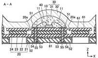
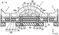
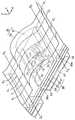
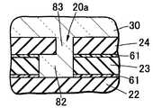
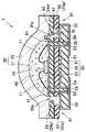
図1に示す本発明の発光装置1は、4枚の基板を積層した積層基板20と、積層基板20の上面20bに載置された発光素子10と、発光素子10及び積層基板20の上面20bとを覆う被覆部材30とから構成されている。<
The
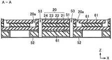
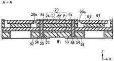
積層基板20は、第1基板21、第2基板22、第3基板23、及び第4積層基板24を順次積層したものである。第1基板21は、他の基板より横幅が狭く、第1基板21と第2基板22との間に矩形の段差が形成されている。第3基板23と第4基板24とにはそれぞれ切断部分があり、互いに連通して溝部20aを形成している。溝部20aは、積層基板20の上面20bに開口している。第2基板22には溝部20aと連通する切断部分はないので、溝部20aの底部が第2基板22の上面になる。
積層基板20の上面20bの中央付近は、発光素子10の載置領域29となっており、一対の上面基板51が形成されている。本発明では、溝部20aは載置領域29に隣接して配置されている。The laminated
Near the center of the
本発明では、溝部20aが被覆部材30を積層基板20に係止する係止構造を有している。この係止構造は、被覆部材30が積層基板20から簡単に脱落しないような構造とするのがよい。例えば、係止構造として、積層基板20の上面20bと垂直方向に形成した一定幅の溝部20aであると、溝部20aを備えない場合に比べて被覆部材30は脱落しにくい。しかしながら、溝部20aの伸びる方向(すなわち、積層基板20の上面20bに対して垂直な方向)に沿って、被覆部材30を上方向に引っ張った場合には比較的脱落を起こしやすいと考えられる。そこで、本発明では、溝部20aを形成することにより、単に積層基板20と被覆部材30との接触面積を増加させて結合力を高めるだけでなく、被覆部材30を積層基板20に機械的手段によって係止することにより、被覆部材30の脱落を効果的に抑制するものである。 In the present invention, the
本実施の形態では、溝部20aに狭幅部分24aと広幅部分23aとを設け、狭幅部分24aが広幅部分23aよりも積層基板20の上面側20bに位置させることにより、係止構造を形成している。これにより、溝部21aに充填された被覆部材30は、広幅部分23aと狭幅部分24aとの段差によって係止されて、積層基板20の上面20b側への引っ張り力によっても脱落しにくい。
図1の例では、狭幅部分24aは第4基板24の切断部分により構成され、広幅部分23aは第3基板23の切断部分により構成されている。In the present embodiment, the
In the example of FIG. 1, the
図1に示す発光装置1では、被覆部材30がシリンドリカルレンズ状に成形されており、発光素子10から放射状に広がる光を、上面方向に効率よく取り出すことができる。
また、この例では、被覆部材30が第1被覆層31と第2被覆層32とを積層して構成されている。第1被覆層31は発光素子10を覆っており、第2被覆層32は、第1被覆層31の上側を覆うように配置されている。このように2層構造になっていると、それぞれに異なる機能を付与することができる。例えば、第1被覆層31又は第2被覆層32のいずれかに蛍光物質40を混入しておけば、発光装置の発光色を、発光素子10の発光色と異ならせることができる。特に、本実施の形態のように、第1被覆層31に蛍光物質40を混入すると、(1)発光素子10の近傍に蛍光物質40を配置することにより、点光源に近づけることができる、(2)少量の蛍光物質であっても所定の色味にすることができる、及び(3)少量の蛍光物質をより効率良く発光させることができる、という点で好ましい。
なお、第1被覆層31、第2被覆層32には、蛍光物質40の他に、必要に応じて光拡散材や酸化防止剤、紫外線反射部材などを含有してもよい。In the
In this example, the covering
In addition to the
本実施の形態では、被覆部材30が2層構造となっているが、この場合には、外側の第2被覆層32が溝部20aに充填されているのが好ましい。これにより、第2被覆層32が基板から抜脱するのを防止できると共に、第1被覆層31の脱落もあわせて防止できるので好ましい。
本発明では、溝部20aは載置領域29に隣接して配置されており、載置領域29の内部には形成されていないので、載置領域29に第1被覆層31を形成し、その外側に第2被覆層32を充填すれば、溝部20aに第2被覆層32を充填することができる。
なお、溝部20aの一部に第1被覆層31が充填されることは問題ない。In the present embodiment, the covering
In the present invention, the
There is no problem that the
溝部20aは、図1の紙面垂直方向に伸びて、積層基板20aの少なくとも一方の側面から外部に露出しているのが好ましい。溝部20aが積層基板20aの側面から露出していると、溝部20a内に被覆部材30を充填するときに溝部20a内の空気が抜けやすくなる。よって、溝部20a内部で被覆部材30に気泡が形成されにくくなるので、被覆部材30が溝部20aに確実に係止でき、被覆部材30と積層基板20との密着性を高めることができるので好ましい。 It is preferable that the
発光素子10として半導体発光素子を使用するときには、発光素子10に過剰な電圧が印加されることのないように、保護素子70が回路内に組み込まれることがある。保護素子70は、発光素子10と同じ載置領域29内に実装されることが多いが、この場合には、保護素子70が発光素子10からの光を遮光し、又は光を吸収することがある。本発明では、保護素子70を溝部20a内に配置することができ、保護素子70による遮光や光吸収の問題が起こらないので好ましい。
ただし、溝部20aの形態によっては、保護素子70への配線がしにくいので、その場合には保護素子70を積層基板20の上面に配置する方が好ましい。When a semiconductor light emitting element is used as the
However, depending on the form of the
積層基板20の載置領域29には、発光素子10が載置されている。そして、発光素子10の正電極又は負電極は、載置領域29に形成された一対の上面電極51の各々に、導電ワイヤ11によって電気的に接続されている。
図1の形態では、一方の上面電極51が大きく形成され、その上に発光素子10が配置されている。これ以外にも、上面電極51を両方とも小さく形成して、発光素子10を積層基板20の上面20bに直接配置してもよい。The
In the form of FIG. 1, one
上面電極21の直下には、積層基板20の上面20bから下面まで貫通するスルーホール53が形成されている。このスルーホール53の内面にはメッキ層54が施され、さらにその内部に穴埋め材料55が充填されている。上面電極51は、メッキ層54を介して下面電極52に電気的に接続されるので、下面電極52と外部電極とを接続すれば、発光素子10を発光させることができる。 A through
積層基板20の積層する際には接着層61が使用できる。接着層61は、第1基板21〜第4基板24の各層の間に配置されている。接着層61は、下面電極52の短絡や、スルーホール53内のメッキ層54間の短絡を防止するために、絶縁性の接着材料が使用される。 When the
次に、本実施の形態に係る発光装置の製造方法について説明する。
(1.積層基板20の作製)
図2には、第1基板21〜第4基板24を積層する前の状態を示す。図示した第1基板21〜第4基板24は、複数個の発光装置1を同時に形成するためのものである。
第1基板21には、横幅一定で所定長さの細長い第1貫通孔81が複数(この例では2つ)ほぼ平行に形成されている。第1基板21の上面、下面及び第1貫通孔81の内壁には、連続する金属膜から成る下面電極52が形成されている。各第1貫通孔81に形成された下面電極52は、上面側で互いに分離されている。この分離部分からは、第1基板21が露出している。Next, a method for manufacturing the light emitting device according to this embodiment will be described.
(1. Production of laminated substrate 20)
FIG. 2 shows a state before the
The
第3基板23には、横幅一定で所定長さの細長い第2貫通孔82が複数(この例では2つ)ほぼ平行に形成されている。
また、第4基板24にも、横幅一定で所定長さの細長い第3貫通孔83が複数(この例では2つ)ほぼ平行に形成されている。第3貫通孔83は、積層したときに第2貫通孔82と連通するように位置決めされている。第3貫通孔83の幅は、第2貫通孔82の幅よりも狭くされている。第4基板24の上面には、連続する金属膜から成る上面電極51が形成されている。なお、第4基板24の下面及び第3貫通孔83の内面には、金属膜が形成されていない。
第2基板22は、貫通孔や金属膜が形成されていない板状体であり、第1貫通孔81と第2貫通孔82との間を分離している。In the
The
The
図2の第1基板21〜第4基板24を、接着シート等の接着層61を間に挟んで積層して、図3Aに示すような積層基板15を形成する。この例では、第2貫通孔82と第3貫通孔83とが連通して形成された溝部20aは、断面L字型になっている。 The
(2.積層基板20の加工)
図4Aのように積層した積層基板20に、第1基板21の下面から第4基板24の上面まで貫通したスルーホール53を複数形成する(図3B参照)。
形成したスルーホール53には、スルーホール53の内面にメッキ層54を施した後、スルーホール34の内部に穴埋め材料55(金属ペースト若しくはエポキシ樹脂等)が充填される。その後、スルーホール34の両端を金属膜で被覆される。金属膜は、メッキ層と電気的に接続され、さらに、上面電極51及び下面電極52と一体にされる。これにより、上面電極16と下面電極27とが電気的に接続される(図4C参照)。(2. Processing of laminated substrate 20)
A plurality of through
The formed through
第4基板24の上面に形成された上面電極51も部分的に除去されて、2つの上面電極51に分離される。また、第1基板21の下面に形成された下面電極52は部分的に除去されて、図3Cに示すような2つの下面電極52に分離される。なお、下面電極52及び上面電極51は、部分的除去の際に、所望の形状に成形することもできる。 The
(3.発光素子18の実装)
次いで、得られた積層基板20に、発光素子10を実装する。発光素子10は、上面電極52にダイボンドされる。そして、発光素子10の電極(図示せず)と、積層基板20の上面電極51とを導電性ワイヤ11によりワイヤボンドする(図3D参照)。複数の発光装置10を同時に製造する場合には、第3貫通孔83の長手方向に沿って複数の発光素子10を配置し、又は第3貫通孔83に直交する方向沿った方向に複数の発光素子10を配置することができる(図4A参照)。
なお、この例では発光素子10を、いわゆるフェイスアップ実装しているが、フリップチップ実装でもよい。(3. Mounting of light emitting element 18)
Next, the
In this example, the
(4.第1被覆部材31及び第2被覆部材32の形成)
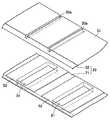
発光素子10及び積層基板20の上面に、第1被覆部材31を形成する(図3E及び図4A参照)。第1被覆部材30の形成では、ライン塗布で形成することができる。本実施の形態でのライン塗布は、第1被覆部材31用の被覆材料を供給するチューブを、溝部20aの長手方向に沿って並んだ発光素子10の上方を移動させながら、複数の発光素子10を連続する第1被覆部材31で被覆する方法である。第1被覆層31は、表面張力により溝部20aに入り込まず、上面電極51上のみに配置する。
本実施の形態では、第1被覆部材31が蛍光物質を含有しているので、ライン塗布に使用する被覆材料に前もって蛍光物質を混合しておくのがよい。(4. Formation of the
A
In the present embodiment, since the
次に、第1被覆部材31を覆うように第2被覆部材32を形成する(図3E及び図4B参照)。第2被覆部材32の形成には、断面形状がシリンドリカル状の金型90を用いることができる。図4Bのように、金型90の凹部91に第2被覆部材32用の被服材料を注入し、そこに逆向きにした積層基板20を押しつけて圧縮成形する。このときに、金型90の凹部91の位置に、積層基板20の上面20bに形成した第1被覆部材31が一致させる。この方法によれば、溝部20aが一方向に長く伸びているので、第2被覆部材32が空気を押出しながら溝部20aの内部にまで侵入しやすい。よって、第2被覆部材32を、溝部20a内に気泡なしで充填することができる。Next, the
(5.発光装置1への分割)
積層基板20をダイシング・ブレードによって分割し、個々の発光装置1に個片化する。詳しくは、図4Cで示すように、溝部20aの伸びている方向(第3貫通孔83の長手方向)と略垂直方向の分割線C1と、溝部20aの伸びている方向と略平行の分割線C2とによって、積層基板20を分割する。分割後は、図3Fに示すように個々の発光装置1が得られる。(5. Division into light-emitting device 1)
The
本実施の形態の製造方法は、第3基板23と第4基板24とに異なる幅の貫通孔82、83を形成し、積層時にそれらの貫通孔を連通させることにより、切削では形成しにくいL字型の溝部20aを容易に形成できる。また、同じ形状の発光装置1を、同時に多数形成することができるので、大量生産に適している。また、小型の発光装置1の製造であっても、比較的ハンドリングしやすい寸法形状の積層基板20で製造して、最後に分割すれば簡単に製造することができる。 In the manufacturing method of the present embodiment, through
本実施の形態では、図4Cにおいて、C1−C1間を狭くして、薄型のサイドビュー型発光装置1を形成しているが、C1−C1間を広くして、トップビュー型の発光装置1を形成することもできる。
また、完成した発光装置1に、さらにシリコーンゴムなどのラバーキャップを被せて使用することもできる。In this embodiment, in FIG. 4C, the space between C <b> 1-C <b> 1 is narrowed to form a thin side view
Further, the completed light emitting
以下、発光装置1の各構成について詳細に説明する。
(積層基板20)
第1基板21〜第4基板24は、適当な機械的強度と絶縁性を有する材料であれば特に限定されない。例えば、アルミナ、窒化アルミニウム、窒化ケイ素、窒化ホウ素などのセラミックス基板や、BTレジン、ガラスエポキシ等を用いることができる。また、エポキシ系樹脂シートを多層張り合わせたものでも良い。
積層基板20に形成された形成する上面電極51及び下面電極52は、Au、Ag、Cu、W、Pt、Rhなどの薄膜から形成できる。薄膜形成方法としては、メッキ、蒸着、スパッタ、印刷等の手法を利用できる。Hereinafter, each structure of the light-emitting
(Laminated substrate 20)
The
The
(発光素子10)
発光素子10には、半導体発光素子が好ましく利用される。特に、バックライト用の白色発光装置を作製する場合には、発光素子に短波長を発する発光ダイオードを用いて、蛍光物質により発光の一部を他の色に波長変換する方法が採用できる。以下に、白色発光装置に利用できる発光ダイオードと蛍光物質との組み合わせについて説明する。(Light emitting element 10)
For the
白色の発光装置を構成するのに適した発光ダイオードとして、窒化物半導体(InXAlYGa1−X−YN、0≦X、0≦Y、X+Y≦1)のを用いたものを用いることができる。この発光ダイオードは、InxGa1-xN(0<x<1)を発光層として有しており、その混晶度によって発光波長を約365nmから650nmで任意に変えることができる。As a light-emitting diode suitable for constituting a white light-emitting device, used after using nitride semiconductor(In X Al Y Ga 1- X-Y N, 0 ≦ X, 0 ≦ Y, X + Y ≦ 1) that the be able to. This light emitting diode has Inx Ga1-x N (0 <x <1) as a light emitting layer, and the light emission wavelength can be arbitrarily changed from about 365 nm to 650 nm depending on the degree of mixed crystal.
白色系の光を発光させる場合は、蛍光物質から出射される光との補色関係を考慮すると、発光ダイオード8の発光波長は400nm以上530nm以下に設定することが好ましく、420nm以上490nm以下に設定することがより好ましい。なお、蛍光物質の種類を選択することにより、400nmより短い紫外域の波長の光を発光するLEDチップを適用することもできる。 When white light is emitted, considering the complementary color relationship with the light emitted from the fluorescent material, the light emission wavelength of the light emitting diode 8 is preferably set to 400 nm or more and 530 nm or less, and is set to 420 nm or more and 490 nm or less. It is more preferable. Note that an LED chip that emits light having an ultraviolet wavelength shorter than 400 nm can also be applied by selecting the type of fluorescent material.
(被覆部材30)
被覆部材30は、第1被覆層31と第2被覆層32とから成っているが、一層のみでも良く、三層以上とすることもできる。複数の層の積層体にすることにより、下層側(例えば第1被覆層31)に耐熱性、耐光性に優れた樹脂を用い、上層側(例えば第2被覆層32)に耐候性に優れた樹脂を用いるなど、各層ごとに異なる物性の被服材料を使用することができる。
第1被覆層31は、シリコーン樹脂、エポキシ樹脂などを配置することができるが、シリコーン樹脂が耐光性の観点から好ましい。
第2被覆層32は、シリコーン樹脂、エポキシ樹脂などを配置することができるが、硬質のシリコーン樹脂若しくはエポキシ樹脂が耐候性の観点から好ましい。(Coating member 30)
The covering
A silicone resin, an epoxy resin, or the like can be disposed on the
A silicone resin, an epoxy resin, or the like can be disposed on the
(蛍光物質40)
蛍光物質40は、発光素子10からの光を吸収し異なる波長の光に波長変換するものであればよい。例えば、Eu、Ce等のランタノイド系元素で主に賦活される窒化物系蛍光物質・酸窒化物系蛍光物質・サイアロン系蛍光物質、Eu等のランタノイド系、Mn等の遷移金属系の元素により主に付活されるアルカリ土類ハロゲンアパタイト蛍光物質、アルカリ土類金属ホウ酸ハロゲン蛍光物質、アルカリ土類金属アルミン酸塩蛍光物質、アルカリ土類ケイ酸塩蛍光物質、アルカリ土類硫化物蛍光物質、アルカリ土類チオガレート蛍光物質、アルカリ土類窒化ケイ素蛍光物質、ゲルマン酸塩蛍光物質、又は、Ce等のランタノイド系元素で主に付活される希土類アルミン酸塩蛍光物質、希土類ケイ酸塩蛍光物質又はEu等のランタノイド系元素で主に賦活される有機及び有機錯体等から選ばれる少なくともいずれか1以上であることが好ましい。具体例として、下記の蛍光物質を使用することができるが、これに限定されない。(Fluorescent substance 40)
The
Eu、Ce等のランタノイド系元素で主に賦活される窒化物系蛍光物質は、M2Si5N8:Eu、MAlSiN3:Eu、MAl1−XBXSiN3:Eu(Mは、Sr、Ca、Ba、Mg、Znから選ばれる少なくとも1種以上である。0<X<1である。)などがある。また、M2Si5N8:EuのほかMSi7N10:Eu、M1.8Si5O0.2N8:Eu、M0.9Si7O0.1N10:Eu(Mは、Sr、Ca、Ba、Mg、Znから選ばれる少なくとも1種以上である。)などもある。The nitride fluorescent materials mainly activated by lanthanoid elements such as Eu and Ce are M2 Si5 N8 : Eu, MAlSiN3 : Eu, MAl1-X BX SiN3 : Eu (M is Sr , Ca, Ba, Mg, and Zn. 0 <X <1). In addition to M2 Si5 N8 : Eu, MSi7 N10 : Eu, M1.8 Si5 O0.2 N8 : Eu, M0.9 Si7 O0.1 N10 : Eu (M Is at least one selected from Sr, Ca, Ba, Mg, and Zn.
Eu、Ce等のランタノイド系元素で主に賦活される酸窒化物系蛍光物質は、MSi2O2N2:Eu(Mは、Sr、Ca、Ba、Mg、Znから選ばれる少なくとも1種以上である。)などがある。An oxynitride fluorescent material mainly activated by a lanthanoid element such as Eu or Ce is MSi2 O2 N2 : Eu (M is at least one selected from Sr, Ca, Ba, Mg, Zn) Etc.).
Eu、Ce等のランタノイド系元素で主に賦活されるサイアロン系蛍光物質は、Mp/2Si12−p−qAlp+qOqN16−p:Ce、M−Al−Si−O−N(Mは、Sr、Ca、Ba、Mg、Znから選ばれる少なくとも1種以上である。qは0〜2.5、pは1.5〜3である。)などがある。Eu, SiAlON-based fluorescent material activated mainly with lanthanoid elements such as Ceis, M p / 2 Si 12- p-q Al p + q O q N 16-p: Ce, M-Al-Si-O-N (M is at least one selected from Sr, Ca, Ba, Mg, and Zn. Q is 0 to 2.5, and p is 1.5 to 3).
Eu等のランタノイド系、Mn等の遷移金属系の元素により主に付活されるアルカリ土類ハロゲンアパタイト蛍光物質には、M5(PO4)3X:R(Mは、Sr、Ca、Ba、Mg、Znから選ばれる少なくとも1種以上である。Xは、F、Cl、Br、Iから選ばれる少なくとも1種以上である。Rは、Eu、Mn、EuとMn、のいずれか1以上である。)などがある。Alkaline earth halogen apatite fluorescent materials mainly activated by lanthanoid-based elements such as Eu and transition metal-based elements such as Mn include M5 (PO4 )3 X: R (M is Sr, Ca, Ba). X is at least one selected from F, Cl, Br and I. R is any one of Eu, Mn, Eu and Mn. Etc.).
アルカリ土類金属ホウ酸ハロゲン蛍光物質には、M2B5O9X:R(Mは、Sr、Ca、Ba、Mg、Znから選ばれる少なくとも1種以上である。Xは、F、Cl、Br、Iから選ばれる少なくとも1種以上である。Rは、Eu、Mn、EuとMn、のいずれか1以上である。)などがある。The alkaline earth metal borate halogen fluorescent substance includes M2 B5 O9 X: R (M is at least one selected from Sr, Ca, Ba, Mg, Zn. X is F, Cl , Br, or I. R is Eu, Mn, or any one of Eu and Mn.).
アルカリ土類金属アルミン酸塩蛍光物質には、SrAl2O4:R、Sr4Al14O25:R、CaAl2O4:R、BaMg2Al16O27:R、BaMg2Al16O12:R、BaMgAl10O17:R(Rは、Eu、Mn、EuとMn、のいずれか1以上である。)などがある。Alkaline earth metal aluminate fluorescent materials include SrAl2 O4 : R, Sr4 Al14 O25 : R, CaAl2 O4 : R, BaMg2 Al16 O27 : R, BaMg2 Al16 O12 : R, BaMgAl10 O17 : R (R is Eu, Mn, or any one of Eu and Mn).
アルカリ土類硫化物蛍光物質には、La2O2S:Eu、Y2O2S:Eu、Gd2O2S:Euなどがある。Examples of the alkaline earth sulfide fluorescent material include La2 O2 S: Eu, Y2 O2 S: Eu, and Gd2 O2 S: Eu.
Ce等のランタノイド系元素で主に賦活される希土類アルミン酸塩蛍光物質には、Y3Al5O12:Ce、(Y0.8Gd0.2)3Al5O12:Ce、Y3(Al0.8Ga0.2)5O12:Ce、(Y,Gd)3(Al,Ga)5O12の組成式で表されるYAG系蛍光物質などがある。また、Yの一部若しくは全部をTb、Lu等で置換したTb3Al5O12:Ce、Lu3Al5O12:Ceなどもある。Rare earth aluminate fluorescent materials mainly activated with lanthanoid elements such as Ce include Y3 Al5 O12 : Ce, (Y0.8 Gd0.2 )3 Al5 O12 : Ce, Y3 (Al0.8 Ga0.2 )5 O12 : Ce, (Y, Gd)3 (Al, Ga)5 O12 There is a YAG-based fluorescent material represented by a composition formula. Further, there are Tb3 Al5 O12 : Ce, Lu3 Al5 O12 : Ce, etc. in which a part or all of Y is substituted with Tb, Lu or the like.
その他の蛍光物質には、ZnS:Eu、Zn2GeO4:Mn、MGa2S4:Eu(Mは、Sr、Ca、Ba、Mg、Znから選ばれる少なくとも1種以上である。Xは、F、Cl、Br、Iから選ばれる少なくとも1種以上である。)などがある。Other fluorescent materials include ZnS: Eu, Zn2 GeO4 : Mn, MGa2 S4 : Eu (M is at least one selected from Sr, Ca, Ba, Mg, Zn. X is At least one selected from F, Cl, Br, and I).
上述の蛍光物質は、所望に応じてEuに代えて、又は、Euに加えてTb、Cu、Ag、Au、Cr、Nd、Dy、Co、Ni、Tiから選択される1種以上を含有させることもできる。
また、上記蛍光物質以外の蛍光物質であって、同様の性能、効果を有する蛍光物質も使用することができる。The above-mentioned fluorescent substance contains at least one selected from Tb, Cu, Ag, Au, Cr, Nd, Dy, Co, Ni, and Ti instead of Eu or in addition to Eu as desired. You can also.
In addition, fluorescent materials other than the above-described fluorescent materials and having the same performance and effect can be used.
これらの蛍光物質は、発光素子の励起光により、黄色、赤色、緑色、青色に発光スペクトルを有する蛍光物質を使用することができるほか、これらの中間色である黄色、青緑色、橙色などに発光スペクトルを有する蛍光物質も使用することができる。これらの蛍光物質を種々組み合わせて使用することにより、種々の発光色を有する表面実装型発光装置を製造することができる。 These fluorescent materials can use fluorescent materials having emission spectra in yellow, red, green, and blue by the excitation light of the light-emitting element, and emission spectra in yellow, blue-green, orange, etc., which are intermediate colors between them. Fluorescent materials having can also be used. By using these fluorescent materials in various combinations, surface-mounted light emitting devices having various emission colors can be manufactured.
例えば、青色に発光するGaN系化合物半導体を用いて、Y3Al5O12:Ce若しくは(Y0.8Gd0.2)3Al5O12:Ceの蛍光物質に照射し、波長変換を行う。発光素子からの光と、蛍光物質からの光との混合色により白色に発光する表面実装型発光装置を提供することができる。For example, using a GaN-based compound semiconductor that emits blue light, a Y3 Al5 O12 : Ce or (Y0.8 Gd0.2 )3 Al5 O12 : Ce fluorescent material is irradiated to convert the wavelength. Do. A surface-mount light-emitting device that emits white light by a mixed color of light from a light-emitting element and light from a fluorescent material can be provided.
例えば、緑色から黄色に発光するCaSi2O2N2:Eu又はSrSi2O2N2:Euと、蛍光物質である青色に発光する(Sr,Ca)5(PO4)3Cl:Eu、赤色に発光するCa2Si5N8:Eu又はCaAlSiN3:Euと、からなる蛍光物質60を使用することによって、演色性の良好な白色に発光する表面実装型発光装置を提供することができる。これは、色の三源色である赤・青・緑を使用しているため、第1の蛍光物質及び第2の蛍光物質の配合比を変えることのみで、所望の白色光を実現することができる。For example, CaSi2 O2 N2 : Eu or SrSi2 O2 N2 : Eu that emits light from green to yellow, and (Sr, Ca)5 (PO4 )3 Cl: Eu that emits blue light as a fluorescent material, By using a fluorescent material 60 composed of Ca2 Si5 N8 : Eu or CaAlSiN3 : Eu that emits red light, a surface-mount light-emitting device that emits white light with good color rendering can be provided. . This uses the three primary colors of red, blue, and green, so that the desired white light can be achieved simply by changing the blend ratio of the first and second fluorescent materials. Can do.
(光拡散材)
発光素子10からの発光を拡散させて、色むらを低減するために、被覆部材30に光拡散材を均一分散させてもよい。特に、第1被覆層31には蛍光物質40を含有させ、第2被覆層32には光拡散材を含有させれば、色むらをより低減することができる。光拡散材は、シリカ、酸化チタン等を使用することができる。(Light diffusing material)
In order to diffuse light emitted from the
<変形例1>
溝部20aの断面形状は、図5AのようなL字型以外に、様々な形態にすることができる。
例えば、図5Bのように、第3基板23の第2貫通孔の幅をさらに広げて、断面形状が逆T字型の溝部20aを形成すれば、被覆部材30を溝部20aに係止する係止力が高まるので好ましい。<
The cross-sectional shape of the
For example, as shown in FIG. 5B, if the width of the second through hole of the
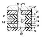
積層する基板の枚数を増やして、それぞれに貫通孔を形成して溝部を形成すれば、より複雑な断面形状の溝部20aを形成することができる。例えば、図5C及び図5Dのように、3枚の基板(第3基板23、第4基板24及び第5基板25)の貫通孔(第2貫通孔82、第3貫通孔83及び第4貫通孔84)から溝部20aを形成すれば、断面形状が横向きのT字(図5C)や十字型(図5D)の溝部20aを形成できる。
さらに、図5E〜図5Gのように、4枚の基板(第3基板23、第4基板24、第5基板25及び第6基板26)の貫通孔(第2貫通孔82、第3貫通孔83、第4貫通孔84及び第5貫通孔85)から溝部20aを形成すれば、断面形状がL字型を2つ組み合わせたような形状(図5E)や、逆T字型を2つ組み合わせたような形状(図5F)や、L字型と逆T字型とを組み合わせたような形状(図5G)など、様々な形状の溝部20aを形成できる。If the number of substrates to be stacked is increased and a through hole is formed in each substrate to form a groove portion, the
Further, as shown in FIGS. 5E to 5G, through holes (second through
また、別の例として、実施の形態1と同様に2枚の基板(第3基板23及び第4基板24)の貫通孔(第2貫通孔82及び第3貫通孔83)とから溝部30aを形成する変形例もある。例えば、図5Hのように、同じ幅の第2貫通孔82と第3貫通孔83から係止構造を構成することもできる。この場合には、第2貫通孔82の中心位置と第3貫通孔83の中心位置をずらして、且つ部分的に連通するように基板を積層する。これにより溝部20aの内部に段差ができるので、充填された被覆部材30を機械的に係止することができる。また、同じ寸法形状の貫通孔が形成された基板を、わずかにずらして積層すればよいので、部品種類を減らすことができる。 As another example, the groove 30a is formed from the through holes (the second through
<実施の形態2>
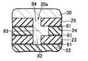
本実施の形態にかかる発光装置1は、図6に図示されているように、積層基板20が、第1基板21〜第3基板23の3枚から形成されていることを除いて、実施の形態1と同様である。
本実施の形態では、積層基板20には、貫通孔を備えていない平板状の基板が含まれていない。そのため、第1基板21の第1貫通孔81と第2基板22の第2貫通孔82とが連通しないように、貫通孔の形成位置を決定しなくてはならない。
本実施の形態では、積層基板20を構成する基板の枚数を少なくできるので、積層基板20の薄型化に適している。<Embodiment 2>
As shown in FIG. 6, the
In the present embodiment, the
In the present embodiment, since the number of substrates constituting the
<実施の形態3>
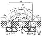
本実施の形態にかかる発光装置1は、図7に図示されているように、積層基板20が、第1基板21と第2基板23の2枚から形成されている点と、溝部20aの断面形状が異なる点を除いて、実施の形態1及び2と同様である。<Embodiment 3>
In the
溝部20aは、積層基板20の上面20bに対して傾斜している。この傾斜により、被覆部材30が積層基板20から脱離するのを防止している。すなわち、溝部20aにこのような傾斜した部分が含まれていれば、係止構造として機能させることができる。
また、載置領域29の両側まで上面電極51が形成されていると、第1被覆層31は表面張力により上面電極51の位置まで山なりに形成される。そして、載置領域29に隣接して溝部20aが形成されているなら、第2被覆層32は、山なりに形成された第1被覆層431に沿って溝部420aに流れ込むことができるので、さらに溝部20aに空気が残存しにくくなる。The
Further, when the
本実施の形態の積層基板20の形成には、図8のように第2基板22の上面に溝部20aを掘削した後に、第1基板21と第2基板22とを積層する。溝部20aの掘削には、ダイシング・ブレード等を使用することができる。 In the formation of the
<実施の形態4>
本実施の形態にかかる発光装置1は、図9に図示されているように、積層基板20の載置領域29が狭くされていることを除いて、実施の形態1と同様である。
本実施の形態では、載置領域29に上面電極51を形成していない。上面電極51は、載置領域29から溝部20aを挟んだ位置に形成されている。よって、発光素子10と上面電極51とを導通するために、溝部20aを越えるように導電ワイヤ11を張ることになる。
本実施の形態では、載置領域29を狭くして、その上面のみに第1被覆層31を配置しているので、第1被覆層に含まれる蛍光物質240の量を少なくすることができる。<Embodiment 4>
The
In the present embodiment, the
In the present embodiment, the
<実施の形態5>
本実施の形態にかかる発光装置1は、図10に図示されているように、積層基板20の載置領域29が、平坦部分29aとテーパー部分29bとから成ることを除いて、実施の形態1と同様である。
載置領域29は、発光素子10を載置する平坦部分29aと、平坦部分29aの両側に形成されて上方向に広がったテーパー部分29bとから構成されている。発光素子10からの発光は、放射状に広がるが、テーパー部分29bによって光反射されると、発光素子の発光の指向性を調節し、光取り出し効率の向上を図ることができる。
また、平坦部分29aとテーパー部分29bとによって形成された凹部に第1被覆層31を形成しているので、ライン塗布では使用できない程度の粘度の低い被覆材料であっても、第1被覆層用の被覆材料として使用することができる。<Embodiment 5>
As shown in FIG. 10, the
The mounting
In addition, since the
本実施の形態では、第1被覆層31は、表面を平らにして載置領域29の凹部内に形成されているので、第2被覆層32との接触面積が狭く、第2被覆層32と積層基板20との密着性が著しく低下する。しかしながら、本発明では、係止構造を備えた溝部20aを積層基板20に形成し、そこに第2被覆層32を充填して、第2被覆層332の抜脱を防止することができる。 In the present embodiment, the
本実施の形態の積層基板20の形成には、図11のように、第4基板24に、上方向に広がったテーパー面29bを備えたテーパー貫通孔290を形成しておき、第1基板21〜第4基板24を積層する。テーパー貫通孔290は、第3基板23の上面によって封止される。よって、載置領域29の平坦部分29aは、第3基板23の上面によって構成される。
なお、第4基板24のテーパー貫通孔290を、テーパー溝部として貫通させず、テーパー溝部の底面を平坦部分29aとすることもできる。In the formation of the
The tapered through
本発明の半導体装置は、液晶ディスプレイのバックライト等のように、極めて薄型の発光部品を必要とする装置を使用する装置に利用可能である。 The semiconductor device of the present invention can be used for a device that uses a device that requires extremely thin light-emitting components, such as a backlight of a liquid crystal display.
10 発光素子
20 積層基板
20a 溝部
21 第1基板
22 第2基板
23 第3基板
24 第4基板
30 被覆部材
31 第1被覆層
32 第2被覆層
40 蛍光物質
51 上面電極
52 下面電極
53 スルーホールDESCRIPTION OF
Claims (16)
Translated fromJapanese複数の基板を積層して構成され、前記発光素子を載置するための載置領域を上面に有する積層基板と、
前記発光素子と前記積層基板の前記上面とを覆う被覆部材と、を備えた発光装置であって、
前記積層基板の前記上面には、前記発光素子の前記載置領域に隣接して有底の溝部が設けられており、
前記被覆部材が、前記発光素子を覆う第1被覆層と、該第1被覆層の上側を覆い且つ前記溝部を充填するように配置された第2被覆層とを含んでおり、
前記溝部が、前記第2被覆層を前記積層基板に係止する係止構造を有しており、
前記複数の基板の各々は、アルミナ、窒化アルミニウム、窒化ケイ素、窒化ホウ素、BTレジン及びガラスエポキシから成る群から選択された材料から形成されていることを特徴とする発光装置。A light emitting element;
A laminated substrate having a plurality of substrates stacked and having a mounting region on the top surface for mounting the light emitting element;
A light-emitting device comprising: a cover member that covers the light-emitting element and the upper surface of the multilayer substrate;
On the upper surface of the multilayer substrate,a bottomed groove is provided adjacent to the placement region of the light emitting element,
The covering member includes a first covering layer that covers the light emitting element, and a second covering layer that is disposed so as to cover the upper side of the first covering layer and fill the groove.
The groove has a locking structure for locking the second coating layer to the laminated substrate,
Each of the plurality of substrates is formed of a material selected from the group consisting of alumina, aluminum nitride, silicon nitride, boron nitride, BT resin, and glass epoxy.
前記狭幅部分が前記広幅部分よりも前記積層基板の前記上面側に配置されて、前記係止構造を構成していることを特徴とする請求項1又は2に記載の発光装置。The groove includes a narrow portion and a wide portion wider than the narrow portion;
3. The light emitting device according to claim 1, wherein the narrow portion is arranged on the upper surface side of the laminated substrate with respect to the wide portion to constitute the locking structure.
前記傾斜部分が前記係止構造を構成していることを特徴とする請求項1乃至4のいずれか1項に記載の発光装置。The groove includes an inclined portion formed obliquely with respect to the upper surface of the laminated substrate;
The light emitting device according to claim 1, wherein the inclined portion constitutes the locking structure.
前記発光素子を載置するための載置領域を上面に有する積層基板と、
前記発光素子と前記積層基板の前記上面とを覆う被覆部材と、を備え、
前記積層基板の前記上面に、前記発光素子の前記載置領域に隣接して溝部が設けられ、
前記溝部に前記被覆部材が充填され、前記被覆部材を前記積層基板に係止する係止構造を有する発光装置を、同時に複数形成できる発光装置の製造方法であって、
(1)複数の基板を積層して、係止構造を有する溝部を備えた積層基板を形成する工程と、
(2)前記積層基板の上面で前記溝部に隣接した前記載置領域に複数個の発光素子を載置する工程と、
(3)前記発光素子及び前記積層基板の上面に被覆部材を形成する工程と、
(4)前記溝部の長手方向と略垂直方向に前記積層基板を切断して、複数の発光装置に個片化する工程と、を有し、
前記被覆部材が第1被覆層と第2被覆層とを含んでおり、
前記被覆部材を形成する工程が、
前記第1被覆層により前記発光素子を覆う過程と、
前記第2被覆層により前記第1被覆層の上面を覆い、かつ、前記溝部に前記第2被覆層を充填する過程と、を含み、
前記第1被覆層は、ライン塗布で形成され、かつ、表面張力により前記溝部に入り込まないように形成されることを特徴とする発光装置の製造方法。A light emitting element;
A laminated substrate having a mounting region on the top surface for mounting the light emitting element;
A covering member that covers the light emitting element and the upper surface of the multilayer substrate;
A groove is provided on the upper surface of the multilayer substrate adjacent to the placement region of the light emitting element,
A method of manufacturing a light emitting device capable of simultaneously forming a plurality of light emitting devices having a locking structure in which the groove member is filled with the covering member and the covering member is locked to the laminated substrate,
(1) Laminating a plurality of substrates to form a laminated substrate having a groove having a locking structure;
(2) placing a plurality of light emitting elements on the placement area adjacent to the groove on the top surface of the multilayer substrate;
(3) forming a covering member on the upper surface of the light emitting element and the laminated substrate;
(4) cutting the laminated substrate in a direction substantially perpendicular to the longitudinal direction of the groove, and singulating into a plurality of light emitting devices,
The covering member includes a first covering layer and a second covering layer;
Forming the covering member comprises:
Covering the light emitting element with the first covering layer;
Covering the upper surface of the first coating layer with the second coating layer, and filling the groove with the second coating layer,
The method of manufacturing a light emitting device, wherein the first coating layer is formed by line coating and is formed so as not to enter the groove due to surface tension.
互いに略平行に形成された複数の細長い第1貫通孔を備えた第1基板と、
前記第1基板の上面側に積層される第2基板と、
互いに略平行に形成された複数の細長い第2貫通孔を備えた第3基板と、
互いに略平行に形成された複数の細長い貫通孔であって、前記第2貫通孔よりも狭幅で、前記第2貫通孔と位置合わせして形成された第3貫通孔を備えた第4基板と、をこの順に積層して前記積層基板を形成し、前記第2貫通孔と前記第3貫通孔とを連通して前記係止構造を有する前記溝部を形成することを含む、請求項11に記載の製造方法。Forming the laminated substrate comprises:
A first substrate having a plurality of elongated first through holes formed substantially parallel to each other;
A second substrate laminated on the upper surface side of the first substrate;
A third substrate having a plurality of elongated second through holes formed substantially parallel to each other;
A fourth substrate having a plurality of elongated through holes formed substantially in parallel with each other and having a third through hole formed to be narrower than the second through hole and aligned with the second through hole. And laminating in this order to form the laminated substrate, and communicating the second through-hole and the third through-hole to form the groove portion having the locking structure. The manufacturing method as described.
互いに略平行に形成された複数の細長い第1貫通孔を備えた第1基板と、
前記第1基板の上面側に積層される第2基板と、
互いに略平行に形成された複数の細長い第2貫通孔を備えた第3基板と、
互いに略平行に形成された複数の細長い貫通孔であって、前記第2貫通孔と同じ寸法で、前記第2貫通孔の位置と部分的に一致するように位置決めされた第3貫通孔を備えた第4基板と、をこの順に積層して前記積層基板を形成し、前記第2貫通孔と前記第3貫通孔とを連通して前記係止構造を有する前記溝部を形成することを含む、請求項11に記載の製造方法。Forming the laminated substrate comprises:
A first substrate having a plurality of elongated first through holes formed substantially parallel to each other;
A second substrate laminated on the upper surface side of the first substrate;
A third substrate having a plurality of elongated second through holes formed substantially parallel to each other;
A plurality of elongated through-holes formed substantially parallel to each other, the third through-hole having the same dimensions as the second through-hole and positioned so as to partially coincide with the position of the second through-hole Forming the laminated substrate in this order, and forming the groove portion having the locking structure by communicating the second through hole and the third through hole. The manufacturing method according to claim 11.
互いに略平行に形成された複数の細長い第1貫通孔を備えた第1基板と、
互いに略平行に形成された複数の細長い貫通孔であって、前記第1貫通孔と異なる位置に形成された第2貫通孔を備えた第2基板と、
互いに略平行に形成された複数の細長い貫通孔であって、前記第2貫通孔よりも狭幅で、前記第2貫通孔と位置合わせして形成された第3貫通孔を備えた第3基板と、をこの順に積層して前記積層基板を形成し、前記第2貫通孔と前記第3貫通孔とを連通して前記係止構造を有する前記溝部を形成することを含む、請求項11に記載の製造方法。Forming the laminated substrate comprises:
A first substrate having a plurality of elongated first through holes formed substantially parallel to each other;
A plurality of elongated through holes formed substantially in parallel with each other, the second substrate having a second through hole formed at a position different from the first through hole;
A third substrate having a plurality of elongated through holes formed substantially in parallel with each other and having a narrower width than the second through hole and formed in alignment with the second through hole And laminating in this order to form the laminated substrate, and communicating the second through-hole and the third through-hole to form the groove portion having the locking structure. The manufacturing method as described.
前記発光素子を載置するための載置領域を上面に有する積層基板と、
前記発光素子と前記積層基板の前記上面とを覆う被覆部材と、を備え、
前記積層基板の前記上面に、前記発光素子の前記載置領域に隣接して溝部が設けられ、
前記溝部に前記被覆部材が充填され、前記被覆部材を前記積層基板に係止する係止構造を有する発光装置を、同時に複数形成できる発光装置の製造方法であって、
(1)互いに略平行に形成された複数の細長い第1貫通孔を備えた第1基板の上面に、
前記溝部に対応した断面形状を有する細長い切削溝が略平行に複数形成された第2基板を、前記切削溝が上面に位置するように積層する工程と、
(2)前記積層基板の上面で前記切削溝に隣接した前記載置領域に複数個の発光素子を載置する工程と、
(3)前記発光素子及び前記積層基板の上面に前記被覆部材を形成する工程と、
(4)前記切削溝の長手方向と略垂直方向に前記積層基板を切断して、複数の発光装置に個片化する工程と、を有し、
前記被覆部材が第1被覆層と第2被覆層とを含んでおり、
前記被覆部材を形成する工程が、
前記第1被覆層により前記発光素子を覆う過程と、
前記第2被覆層により前記第1被覆層の上面を覆い、かつ、前記溝部に前記第2被覆層を充填する過程と、を含み、
前記第1被覆層は、ライン塗布で形成され、かつ、表面張力により前記溝部に入り込まないように形成されることを特徴とする発光装置の製造方法。A light emitting element;
A laminated substrate having a mounting region on the top surface for mounting the light emitting element;
A covering member that covers the light emitting element and the upper surface of the multilayer substrate;
A groove is provided on the upper surface of the multilayer substrate adjacent to the placement region of the light emitting element,
A method of manufacturing a light emitting device capable of simultaneously forming a plurality of light emitting devices having a locking structure in which the groove member is filled with the covering member and the covering member is locked to the laminated substrate,
(1) On the upper surface of the first substrate provided with a plurality of elongated first through holes formed substantially parallel to each other,
Laminating a second substrate on which a plurality of elongated cutting grooves having a cross-sectional shape corresponding to the groove portions are formed substantially in parallel so that the cutting grooves are positioned on the upper surface;
(2) placing a plurality of light emitting elements on the placement area adjacent to the cutting groove on the top surface of the multilayer substrate;
(3) forming the covering member on the light emitting element and the upper surface of the laminated substrate;
(4) cutting the laminated substrate in a direction substantially perpendicular to the longitudinal direction of the cutting groove, and dividing into a plurality of light emitting devices,
The covering member includes a first covering layer and a second covering layer;
Forming the covering member comprises:
Covering the light emitting element with the first covering layer;
Covering the upper surface of the first coating layer with the second coating layer, and filling the groove with the second coating layer,
The method of manufacturing a light emitting device, wherein the first coating layer is formed by line coating and is formed so as not to enter the groove due to surface tension.
Priority Applications (1)
| Application Number | Priority Date | Filing Date | Title |
|---|---|---|---|
| JP2006330175AJP5315607B2 (en) | 2006-12-07 | 2006-12-07 | Light emitting device and manufacturing method thereof |
Applications Claiming Priority (1)
| Application Number | Priority Date | Filing Date | Title |
|---|---|---|---|
| JP2006330175AJP5315607B2 (en) | 2006-12-07 | 2006-12-07 | Light emitting device and manufacturing method thereof |
Publications (2)
| Publication Number | Publication Date |
|---|---|
| JP2008147270A JP2008147270A (en) | 2008-06-26 |
| JP5315607B2true JP5315607B2 (en) | 2013-10-16 |
Family
ID=39607142
Family Applications (1)
| Application Number | Title | Priority Date | Filing Date |
|---|---|---|---|
| JP2006330175AExpired - Fee RelatedJP5315607B2 (en) | 2006-12-07 | 2006-12-07 | Light emitting device and manufacturing method thereof |
Country Status (1)
| Country | Link |
|---|---|
| JP (1) | JP5315607B2 (en) |
Families Citing this family (18)
| Publication number | Priority date | Publication date | Assignee | Title |
|---|---|---|---|---|
| JP2009182072A (en)* | 2008-01-30 | 2009-08-13 | Toyoda Gosei Co Ltd | Semiconductor light emitting device |
| US20100127288A1 (en)* | 2008-11-25 | 2010-05-27 | Visera Technologies Company Limited | Light-emitting diode devices and methods for fabricating the same |
| JP2013093340A (en)* | 2010-02-26 | 2013-05-16 | Sanyo Electric Co Ltd | Light emitting device |
| JP5370238B2 (en)* | 2010-03-30 | 2013-12-18 | 豊田合成株式会社 | Method for manufacturing light emitting device |
| JP5431259B2 (en)* | 2010-06-30 | 2014-03-05 | シャープ株式会社 | LIGHT EMITTING ELEMENT PACKAGE AND ITS MANUFACTURING METHOD, LIGHT EMITTING ELEMENT ARRAY, AND DISPLAY DEVICE |
| JP2014026993A (en)* | 2010-11-08 | 2014-02-06 | Panasonic Corp | Ceramic substrate and light emitting diode module |
| JP2012212794A (en)* | 2011-03-31 | 2012-11-01 | Stanley Electric Co Ltd | Side emitting and receiving optical semiconductor device for surface mounting and module using the same |
| CN107768502B (en)* | 2011-05-16 | 2019-07-05 | 日亚化学工业株式会社 | Light-emitting device and method of manufacturing the same |
| JP2015041722A (en)* | 2013-08-23 | 2015-03-02 | 株式会社東芝 | Semiconductor light-emitting device |
| JP2015153844A (en)* | 2014-02-13 | 2015-08-24 | 日亜化学工業株式会社 | Light emitting device |
| DE102016100585A1 (en) | 2016-01-14 | 2017-07-20 | Epcos Ag | Device substrate with protective function and method of manufacture |
| JP6432656B2 (en)* | 2017-08-22 | 2018-12-05 | 日亜化学工業株式会社 | Light emitting device |
| JP6989763B2 (en)* | 2017-08-31 | 2022-01-12 | 日亜化学工業株式会社 | Manufacturing method of light emitting device |
| KR102550291B1 (en)* | 2018-01-16 | 2023-07-03 | 쑤저우 레킨 세미컨덕터 컴퍼니 리미티드 | Light emitting device package and light source unit |
| US12130008B2 (en) | 2020-11-27 | 2024-10-29 | Kyocera Corporation | Light emission device and illumination apparatus |
| JP7231846B2 (en)* | 2020-11-30 | 2023-03-02 | 日亜化学工業株式会社 | Method for manufacturing light emitting device |
| US12125953B2 (en) | 2020-11-30 | 2024-10-22 | Nichia Corporation | Method for manufacturing light emitting device, light emitting device, and light emitting module |
| JPWO2023162505A1 (en)* | 2022-02-25 | 2023-08-31 |
Family Cites Families (12)
| Publication number | Priority date | Publication date | Assignee | Title |
|---|---|---|---|---|
| JPH1145961A (en)* | 1997-05-26 | 1999-02-16 | Seiko Epson Corp | Semiconductor device |
| JP3784976B2 (en)* | 1998-12-22 | 2006-06-14 | ローム株式会社 | Semiconductor device |
| JP2004200410A (en)* | 2002-12-18 | 2004-07-15 | Kyocera Corp | Light emitting element storage package and light emitting device |
| JP2004207621A (en)* | 2002-12-26 | 2004-07-22 | Kyocera Corp | Light emitting element storage package and light emitting device |
| JP4307090B2 (en)* | 2003-01-27 | 2009-08-05 | 京セラ株式会社 | Light emitting element storage package and light emitting device |
| EP1659642A4 (en)* | 2003-08-26 | 2011-07-06 | Sumitomo Electric Industries | SEMICONDUCTOR LIGHT-EMITTING DEVICE ELEMENT, MEMBER COMPRISING A LUMINOUS DIODE USING THE SAME, AND LUMINOUS DIODE USING SAME |
| JP2006093486A (en)* | 2004-09-27 | 2006-04-06 | Kyocera Corp | Light emitting element mounting substrate and light emitting device |
| JP2006128512A (en)* | 2004-10-29 | 2006-05-18 | Ngk Spark Plug Co Ltd | Ceramic substrate for light emitting element |
| JP4492378B2 (en)* | 2005-02-03 | 2010-06-30 | 豊田合成株式会社 | Light emitting device and manufacturing method thereof |
| JP2007027433A (en)* | 2005-07-15 | 2007-02-01 | Mitsubishi Cable Ind Ltd | Light emitting device |
| JP2007234846A (en)* | 2006-03-01 | 2007-09-13 | Ngk Spark Plug Co Ltd | Ceramic package for light emitting device |
| JP4822980B2 (en)* | 2006-08-11 | 2011-11-24 | 京セラ株式会社 | Electronic component mounting substrate, electronic device, and method of manufacturing electronic device |
- 2006
- 2006-12-07JPJP2006330175Apatent/JP5315607B2/ennot_activeExpired - Fee Related
Also Published As
| Publication number | Publication date |
|---|---|
| JP2008147270A (en) | 2008-06-26 |
Similar Documents
| Publication | Publication Date | Title |
|---|---|---|
| JP5315607B2 (en) | Light emitting device and manufacturing method thereof | |
| US10825968B2 (en) | Method for manufacturing light-emitting device | |
| JP5103831B2 (en) | Semiconductor manufacturing method | |
| JP5540466B2 (en) | Light emitting device and manufacturing method thereof | |
| JP5123466B2 (en) | Light emitting device | |
| CN107665940B (en) | Light-emitting device and method of manufacturing the same | |
| KR102161062B1 (en) | Light-emitting device | |
| JP2017188592A (en) | Light emitting device | |
| KR102553755B1 (en) | Light-emitting device | |
| CN106299080A (en) | Light emitting device and method for manufacturing the same | |
| JP6978697B2 (en) | Manufacturing method of light emitting device | |
| US10504876B2 (en) | Light-emitting device | |
| JP2008270781A (en) | Light emitting device | |
| US10840415B2 (en) | Method for manufacturing light-transmissive member and method for manufacturing light-emitting device | |
| KR20200112782A (en) | Light-emitting module | |
| JP2007234968A (en) | LIGHT EMITTING DEVICE MANUFACTURING METHOD AND LIGHT EMITTING DEVICE | |
| JP4617761B2 (en) | Method for manufacturing light emitting device | |
| TWI793234B (en) | Light emitting device | |
| JP7295408B2 (en) | Method for manufacturing light emitting device | |
| US10439097B2 (en) | Method for manufacturing light emitting device | |
| KR102728058B1 (en) | Light emitting device | |
| JP2016004981A (en) | Light emission device | |
| JP6658829B2 (en) | Light emitting device manufacturing method | |
| JP2008171931A (en) | Light emitting device | |
| JP4952235B2 (en) | Light emitting device and backlight using the same |
Legal Events
| Date | Code | Title | Description |
|---|---|---|---|
| A621 | Written request for application examination | Free format text:JAPANESE INTERMEDIATE CODE: A621 Effective date:20091116 | |
| A977 | Report on retrieval | Free format text:JAPANESE INTERMEDIATE CODE: A971007 Effective date:20110907 | |
| A131 | Notification of reasons for refusal | Free format text:JAPANESE INTERMEDIATE CODE: A131 Effective date:20120918 | |
| A521 | Request for written amendment filed | Free format text:JAPANESE INTERMEDIATE CODE: A523 Effective date:20121114 | |
| A131 | Notification of reasons for refusal | Free format text:JAPANESE INTERMEDIATE CODE: A131 Effective date:20121204 | |
| A521 | Request for written amendment filed | Free format text:JAPANESE INTERMEDIATE CODE: A523 Effective date:20130201 | |
| A02 | Decision of refusal | Free format text:JAPANESE INTERMEDIATE CODE: A02 Effective date:20130219 | |
| A521 | Request for written amendment filed | Free format text:JAPANESE INTERMEDIATE CODE: A523 Effective date:20130517 | |
| A911 | Transfer to examiner for re-examination before appeal (zenchi) | Free format text:JAPANESE INTERMEDIATE CODE: A911 Effective date:20130527 | |
| TRDD | Decision of grant or rejection written | ||
| A01 | Written decision to grant a patent or to grant a registration (utility model) | Free format text:JAPANESE INTERMEDIATE CODE: A01 Effective date:20130611 | |
| A61 | First payment of annual fees (during grant procedure) | Free format text:JAPANESE INTERMEDIATE CODE: A61 Effective date:20130624 | |
| R150 | Certificate of patent or registration of utility model | Ref document number:5315607 Country of ref document:JP Free format text:JAPANESE INTERMEDIATE CODE: R150 Free format text:JAPANESE INTERMEDIATE CODE: R150 | |
| R250 | Receipt of annual fees | Free format text:JAPANESE INTERMEDIATE CODE: R250 | |
| R250 | Receipt of annual fees | Free format text:JAPANESE INTERMEDIATE CODE: R250 | |
| R250 | Receipt of annual fees | Free format text:JAPANESE INTERMEDIATE CODE: R250 | |
| R250 | Receipt of annual fees | Free format text:JAPANESE INTERMEDIATE CODE: R250 | |
| R250 | Receipt of annual fees | Free format text:JAPANESE INTERMEDIATE CODE: R250 | |
| R250 | Receipt of annual fees | Free format text:JAPANESE INTERMEDIATE CODE: R250 | |
| LAPS | Cancellation because of no payment of annual fees |