JP5315156B2 - Manufacturing method of sensor substrate - Google Patents
Manufacturing method of sensor substrateDownload PDFInfo
- Publication number
- JP5315156B2 JP5315156B2JP2009173430AJP2009173430AJP5315156B2JP 5315156 B2JP5315156 B2JP 5315156B2JP 2009173430 AJP2009173430 AJP 2009173430AJP 2009173430 AJP2009173430 AJP 2009173430AJP 5315156 B2JP5315156 B2JP 5315156B2
- Authority
- JP
- Japan
- Prior art keywords
- conductive
- layer
- containing liquid
- insulating layer
- conductive component
- Prior art date
- Legal status (The legal status is an assumption and is not a legal conclusion. Google has not performed a legal analysis and makes no representation as to the accuracy of the status listed.)
- Expired - Fee Related
Links
Images


Classifications
- G—PHYSICS
- G01—MEASURING; TESTING
- G01N—INVESTIGATING OR ANALYSING MATERIALS BY DETERMINING THEIR CHEMICAL OR PHYSICAL PROPERTIES
- G01N27/00—Investigating or analysing materials by the use of electric, electrochemical, or magnetic means
- G01N27/02—Investigating or analysing materials by the use of electric, electrochemical, or magnetic means by investigating impedance
- G01N27/04—Investigating or analysing materials by the use of electric, electrochemical, or magnetic means by investigating impedance by investigating resistance
- G01N27/12—Investigating or analysing materials by the use of electric, electrochemical, or magnetic means by investigating impedance by investigating resistance of a solid body in dependence upon absorption of a fluid; of a solid body in dependence upon reaction with a fluid, for detecting components in the fluid
- Y—GENERAL TAGGING OF NEW TECHNOLOGICAL DEVELOPMENTS; GENERAL TAGGING OF CROSS-SECTIONAL TECHNOLOGIES SPANNING OVER SEVERAL SECTIONS OF THE IPC; TECHNICAL SUBJECTS COVERED BY FORMER USPC CROSS-REFERENCE ART COLLECTIONS [XRACs] AND DIGESTS
- Y10—TECHNICAL SUBJECTS COVERED BY FORMER USPC
- Y10T—TECHNICAL SUBJECTS COVERED BY FORMER US CLASSIFICATION
- Y10T29/00—Metal working
- Y10T29/49—Method of mechanical manufacture
- Y10T29/49002—Electrical device making
- Y10T29/49117—Conductor or circuit manufacturing
- Y10T29/49124—On flat or curved insulated base, e.g., printed circuit, etc.
- Y10T29/49126—Assembling bases
- Y—GENERAL TAGGING OF NEW TECHNOLOGICAL DEVELOPMENTS; GENERAL TAGGING OF CROSS-SECTIONAL TECHNOLOGIES SPANNING OVER SEVERAL SECTIONS OF THE IPC; TECHNICAL SUBJECTS COVERED BY FORMER USPC CROSS-REFERENCE ART COLLECTIONS [XRACs] AND DIGESTS
- Y10—TECHNICAL SUBJECTS COVERED BY FORMER USPC
- Y10T—TECHNICAL SUBJECTS COVERED BY FORMER US CLASSIFICATION
- Y10T29/00—Metal working
- Y10T29/49—Method of mechanical manufacture
- Y10T29/49002—Electrical device making
- Y10T29/49117—Conductor or circuit manufacturing
- Y10T29/49124—On flat or curved insulated base, e.g., printed circuit, etc.
- Y10T29/49155—Manufacturing circuit on or in base
Landscapes
- Chemical & Material Sciences (AREA)
- Chemical Kinetics & Catalysis (AREA)
- Electrochemistry (AREA)
- Physics & Mathematics (AREA)
- Health & Medical Sciences (AREA)
- Life Sciences & Earth Sciences (AREA)
- Analytical Chemistry (AREA)
- Biochemistry (AREA)
- General Health & Medical Sciences (AREA)
- General Physics & Mathematics (AREA)
- Immunology (AREA)
- Pathology (AREA)
- Investigating Or Analyzing Materials By The Use Of Fluid Adsorption Or Reactions (AREA)
- Investigating Or Analyzing Materials By The Use Of Electric Means (AREA)
Description
Translated fromJapanese本発明は、センサ基板の製造方法、および、その製造方法により得られるセンサ基板に関し、詳しくは、主としてガスの種類や量を検知するためのセンサ基板の製造方法、および、その製造方法により得られるセンサ基板に関する。 The present invention relates to a sensor substrate manufacturing method and a sensor substrate obtained by the manufacturing method, and more specifically, a sensor substrate manufacturing method for detecting mainly the type and amount of gas, and the manufacturing method thereof. The present invention relates to a sensor substrate.
従来より、気体や液体を検知する物質センサが種々の産業用途に用いられている。このような物質センサは、特定の気体や液体における定性分析や定量分析などに用いられている。
例えば、導電性物質を含むレジスタと、互いに間隔を隔てて配置され、レジスタを介して電気的に接続される第1および第2の導電性リードとを備えるセンサアレイを複数設けることが提案されている(例えば、特許文献1参照。)。Conventionally, a substance sensor for detecting gas or liquid has been used for various industrial applications. Such a substance sensor is used for qualitative analysis or quantitative analysis in a specific gas or liquid.
For example, it has been proposed to provide a plurality of sensor arrays each including a register including a conductive material and first and second conductive leads that are spaced apart from each other and electrically connected via the register. (For example, refer to Patent Document 1).
しかるに、特許文献1では、各センサアレイのレジスタに対応する導電性物質、および、その導電性物質を溶解する溶媒を含む溶液を、第1および第2の導電性リードと接触するようにそれぞれ塗布した後、乾燥することにより、各レジスタを形成している(溶液キャスティング)。また、その溶液を、エアスプレー法によって塗布することも知られている。 However, in
しかし、上記した溶液を第1および第2の導電性リードの上に単に塗布、あるいは、エアスプレー法により塗布すると、塗布した後、乾燥するまでの間に、濡れ広がりが発生する。そのため、溶液中の溶媒が蒸発する際、溶液に含まれている導電性物質が、凝集および/または偏在化し、これにより、形成されたレジスタの厚みや拡がりが不均一になる場合がある。その結果、上記した方法によって形成されたレジスタでは、物質を精度良く検知することができない場合がある。また、上記した方法では、上記した溶液の過剰塗布または飛散などにより、材料のロスが発生するという不具合がある。 However, when the above-described solution is simply applied on the first and second conductive leads or is applied by an air spray method, wetting and spreading occur after application and until drying. For this reason, when the solvent in the solution evaporates, the conductive substance contained in the solution is aggregated and / or unevenly distributed, which may result in uneven thickness and spread of the formed resistor. As a result, the register formed by the above-described method may not be able to detect the substance with high accuracy. In addition, the above-described method has a problem that material loss occurs due to excessive application or scattering of the above-described solution.
本発明の目的は、導電性層が均一な厚みで形成されることにより、物質を優れた精度で検知することのできるセンサ基板を製造することのできるセンサ基板の製造方法、および、その製造方法によって得られるセンサ基板を提供することにある。 An object of the present invention is to provide a sensor substrate manufacturing method capable of manufacturing a sensor substrate capable of detecting a substance with excellent accuracy by forming a conductive layer with a uniform thickness, and a manufacturing method thereof. Is to provide a sensor substrate obtained.
上記目的を達成するため、本発明のセンサ基板の製造方法は、絶縁層を用意する工程と、前記絶縁層の上に、少なくとも1対の電極を形成する工程と、前記電極を被覆するように、前記絶縁層の上に、導電性成分含有液を超音波スプレー法により噴き付けて、導電性層を形成する工程とを備えることを特徴としている。
また、本発明のセンサ基板の製造方法では、前記導電性成分含有液が、有機溶剤、導電性粒子および非導電性物質を含むことが好適である。In order to achieve the above object, a method of manufacturing a sensor substrate according to the present invention includes a step of preparing an insulating layer, a step of forming at least one pair of electrodes on the insulating layer, and a step of covering the electrodes. And a step of spraying a conductive component-containing liquid on the insulating layer by an ultrasonic spray method to form a conductive layer.
In the sensor substrate manufacturing method of the present invention, it is preferable that the conductive component-containing liquid contains an organic solvent, conductive particles, and a non-conductive substance.
また、本発明のセンサ基板の製造方法では、前記導電性成分含有液の25℃における粘度が、0.05Pa・s以下であることが好適である。
また、本発明は、上記したセンサ基板の製造方法により得られる、センサ基板を含んでいる。In the method for producing a sensor substrate of the present invention, it is preferable that a viscosity at 25 ° C. of the conductive component-containing liquid is 0.05 Pa · s or less.
In addition, the present invention includes a sensor substrate obtained by the above-described method for manufacturing a sensor substrate.
本発明のセンサ基板の製造方法によれば、導電性層を均一に形成することができる。
また、本発明のセンサ基板の製造方法によれば、導電性成分含有液のロスが少なく、そのため、センサ基板の製造におけるコストを、低減することができる。
また、このようなセンサ基板の製造方法により得られるセンサ基板によれば、物質の検知を、確実、かつ、優れた精度で実施することができる。According to the method for manufacturing a sensor substrate of the present invention, the conductive layer can be formed uniformly.
In addition, according to the method for manufacturing a sensor substrate of the present invention, the loss of the conductive component-containing liquid is small, and therefore the cost in manufacturing the sensor substrate can be reduced.
Moreover, according to the sensor substrate obtained by such a method for manufacturing a sensor substrate, the substance can be detected reliably and with excellent accuracy.
図1は、本発明のセンサ基板の製造方法により得られるセンサ基板の一実施形態の平面図、図2は、図1のA−A線における断面図、図3は、図1に示すセンサ基板の製造方法を示す製造工程図を示す。なお、導体パターンの相対配置を明確に示すために、図1においては、保護層11を省略している。
図1において、このセンサ基板1は、絶縁層としてのベース絶縁層2と、ベース絶縁層2の上に形成される導体パターン8とを備えている。FIG. 1 is a plan view of an embodiment of a sensor substrate obtained by the method for manufacturing a sensor substrate of the present invention, FIG. 2 is a cross-sectional view taken along line AA in FIG. 1, and FIG. 3 is a sensor substrate shown in FIG. The manufacturing process figure which shows this manufacturing method is shown. In order to clearly show the relative arrangement of the conductor patterns, the
In FIG. 1, the
ベース絶縁層2は、例えば、長手方向に延びる矩形状のシートから形成されている。
導体パターン8は、ベース絶縁層2の表面において、1対の配線6を備える配線回路パターンとして形成されている。
1対の配線6は、長手方向と直交する方向(以下、幅方向という。)に互いに間隔を隔てて対向配置され、長手方向に沿って延びるように形成されている。The
The conductor pattern 8 is formed as a wiring circuit pattern including a pair of wirings 6 on the surface of the
The pair of wirings 6 are arranged so as to face each other at intervals in a direction orthogonal to the longitudinal direction (hereinafter referred to as the width direction) and extend along the longitudinal direction.
具体的には、1対の配線6は、幅方向一方側に配置される第1配線6Aと、幅方向他方側に配置される第2配線6Bとを備えている。また、1対の配線6は、その長手方向一方側端部において、対向方向内側に屈曲して、電気抵抗検知器10と接続されている。
また、導体パターン8には、図2に示すように、導体パターン8を被覆する保護層11が形成されている。Specifically, the pair of wirings 6 includes a
Further, as shown in FIG. 2, a
保護層11は、第1配線6Aおよび第2配線6Bの表面(上面および側面)に直接形成されている。
そして、このように形成されるセンサ基板1は、検知部3を備えている。
検知部3は、センサ基板1において物質を検知する領域であって、図1に示されるように、ベース絶縁層2の上において、平面視略矩形状に区画されている。また、検知部3は、1対(2つ)の電極5と導電性層7とを備えている。The
The
The
すなわち、1対の電極5は、1対の配線6において、検知部3の領域内に含まれる部分とされている。また、1対の電極5において、第1配線6Aに対応する電極5が第1電極5Aとされ、第2配線6Bに対応する電極5が第2電極5Bとされている。
導電性層7は、ベース絶縁層2の上において、1対の電極5を被覆するように、平面視略矩形状に形成され、検知部3の外形形状を画成している。That is, the pair of electrodes 5 is a portion included in the region of the
The
より具体的には、導電性層7は、ベース絶縁層2の上面において、保護層11の表面と、保護層11から露出するベース絶縁層2の上面とに接触するように、形成されている。これにより、導電性層7は、第1電極5Aおよび第2電極5B間にわたって、第1電極5Aおよび第2電極5Bと電気的に接続されている。
次に、このセンサ基板1を製造する方法について、図3を参照して説明する。More specifically, the
Next, a method for manufacturing the
まず、この方法では、図3(a)に示すように、ベース絶縁層2を用意する。
ベース絶縁層2を形成する絶縁材料としては、例えば、液晶ポリマー(LCP;芳香族または脂肪族ジヒドロキシ化合物の重合体、芳香族または脂肪族ジカルボン酸の重合体、芳香族ヒドロキシカルボン酸の重合体、芳香族ジアミン、芳香族ヒドロキシアミンまたは芳香族アミノカルボン酸の重合体など)、ポリエチレンテレフタレート(PET)、ポリイミド(PI)、ポリエーテルニトリル、ポリエーテルスルホン、ポリエチレンナフタレート、ポリフェニリンサルファイド(PPS)、ポリエーテルイミド(PEI)、ポリ塩化ビニルなどの合成樹脂などが用いられる。これら絶縁材料は、単独使用または併用することができる。First, in this method, the
Examples of the insulating material forming the
また、このような絶縁材料としては、好ましくは、吸水率、湿度膨張係数、熱膨張係数およびガス透過率が低い材料が用いられる。
好ましくは、液晶ポリマーまたはポリエチレンテレフタレートが用いられる。液晶ポリマーまたはポリエチレンテレフタレートは、吸水率やガス透過率(酸素透過率など)が低いため、雰囲気中の水蒸気の吸水によりベース絶縁層2が膨潤することを防止でき、また、ベース絶縁層2の下面からガスや水蒸気が透過して、導電性層7に影響を与えることを防止できる。従って、そのようなベース絶縁層2の膨潤に基づく誤検知や、ベース絶縁層2の透過の影響に基づく誤検知を、防止することができる。Further, as such an insulating material, a material having a low water absorption rate, a humidity expansion coefficient, a thermal expansion coefficient, and a gas permeability is preferably used.
Preferably, liquid crystal polymer or polyethylene terephthalate is used. Since the liquid crystal polymer or polyethylene terephthalate has a low water absorption rate and gas transmission rate (oxygen transmission rate, etc.), the
ベース絶縁層2を用意するには、例えば、上記した絶縁材料のシートを準備する。また、図示しない剥離板の上に、絶縁材料のワニスをキャスティングにより成膜し、乾燥後、必要により硬化させることにより、用意することもできる。
なお、上記した絶縁材料のシートとしては、市販品を用いることができ、例えば、ベクスターシリーズ(液晶ポリマーシート、クラレ社製)、BIACシリーズ(液晶ポリマーシート、ジャパンゴアテックス社製)、ルミラーシリーズ(ポリエチレンテレフタレートシート、東レ社製)などが用いられる。In order to prepare the
In addition, as a sheet | seat of an above-mentioned insulating material, a commercial item can be used, for example, a Bexter series (a liquid crystal polymer sheet, the Kuraray company make), a BIAC series (a liquid crystal polymer sheet, the Japan Gore-Tex company make), a lumirror series ( A polyethylene terephthalate sheet (manufactured by Toray Industries, Inc.) is used.
このようにして形成されるベース絶縁層2の厚みは、例えば、5〜30μm、好ましくは、5〜25μmである。
次いで、この方法では、図3(b)に示すように、導体パターン8を、ベース絶縁層2の上に、形成する。
導体パターン8を形成する材料としては、例えば、銅、ニッケル、金、錫、ロジウム、はんだ、またはこれらの合金などの導体材料が用いられ、好ましくは、導電性および加工性の観点から、銅が用いられる。The
Next, in this method, the conductor pattern 8 is formed on the
As a material for forming the conductor pattern 8, for example, a conductor material such as copper, nickel, gold, tin, rhodium, solder, or an alloy thereof is used. Preferably, from the viewpoint of conductivity and workability, copper is used. Used.
導体パターン8は、例えば、印刷法、アディティブ法、サブトラクティブ法などの公知のパターンニング法によって、上記した配線回路パターンとして形成する。
印刷法では、例えば、上記した材料の微粒子を含むペーストを、ベース絶縁層2の表面に、上記したパターンでスクリーン印刷した後、焼結する。これにより、導体パターン8を、ベース絶縁層2の表面に、直接形成する。The conductor pattern 8 is formed as the above-described wiring circuit pattern by a known patterning method such as a printing method, an additive method, or a subtractive method.
In the printing method, for example, a paste containing fine particles of the above-described material is screen-printed on the surface of the
アディティブ法では、例えば、まず、ベース絶縁層2の表面に、図示しない導体薄膜(種膜)を形成する。導体薄膜は、スパッタリング、好ましくは、クロムスパッタリングおよび銅スパッタリングにより、クロム薄膜と銅薄膜とを順次積層する。
次いで、この導体薄膜の表面に、上記した導体パターンと逆パターンでめっきレジストを形成した後、めっきレジストから露出する導体薄膜の表面に、電解めっきにより、導体パターン8を形成する。その後、めっきレジストおよびそのめっきレジストが積層されていた部分の導体薄膜を除去する。In the additive method, for example, a conductor thin film (seed film) (not shown) is first formed on the surface of the
Next, after forming a plating resist on the surface of the conductor thin film in a pattern opposite to the above-described conductor pattern, a conductor pattern 8 is formed on the surface of the conductor thin film exposed from the plating resist by electrolytic plating. Thereafter, the plating resist and the conductor thin film where the plating resist was laminated are removed.
サブトラクティブ法では、例えば、まず、ベース絶縁層2の表面に、上記した導体材料からなる導体層が予め積層されている2層基材(銅箔2層基材など)を用意し、その導体層の上に、ドライフィルムレジストを積層した後、露光および現像し、上記した導体パターン8と同一のパターンのエッチングレジストを形成する。その後、エッチングレジストから露出する導体層を化学エッチング(ウェットエッチング)した後、エッチングレジストを除去することにより、導体パターン8を形成する。なお、2層基材の用意において、必要により、ベース絶縁層2と導体層との間に、公知の接着剤層を介在させることもできる。 In the subtractive method, for example, first, a two-layer base material (such as a copper foil two-layer base material) in which a conductor layer made of the above-described conductor material is previously laminated on the surface of the
なお、上記したサブトラクティブ法による導体パターン8の形成において、銅箔2層基材としては、市販品を用いることができ、例えば、液晶ポリマーからなるベース絶縁層2の表面に、銅からなら導体層が予め積層されている液晶ポリマー銅張積層板(ESPANEX Lシリーズ、片面品、標準タイプ/Pタイプ、新日鐵化学社製)が用いられる。
これらのパターンニング法において、好ましくは、印刷法が用いられる。この方法によれば、導体パターン8を、ベース絶縁層2の表面に、確実に直接形成できるので、特定のガスの検知を、精度よく実施することができる。In the formation of the conductor pattern 8 by the subtractive method described above, a commercially available product can be used as the copper foil two-layer base material. A liquid crystal polymer copper-clad laminate (ESPANEX L series, single-sided product, standard type / P type, manufactured by Nippon Steel Chemical Co., Ltd.) in which layers are laminated in advance is used.
In these patterning methods, a printing method is preferably used. According to this method, since the conductor pattern 8 can be reliably formed directly on the surface of the insulating
このようにして形成される導体パターン8の厚みは、例えば、5〜30μm、好ましくは、5〜20μmである。また、各配線6の長さ(長手方向長さ)は、同一または相異なっていてもよく、例えば、5〜100mm、好ましくは、5〜50mmである。各配線6(電極5)の幅(幅方向長さ)は、例えば、10〜500μm、好ましくは、20〜300μmである。また、各配線6(電極5)間の間隔は、例えば、0.1〜10mm、好ましくは、0.2〜4mmである。 Thus, the thickness of the conductor pattern 8 formed is 5-30 micrometers, for example, Preferably, it is 5-20 micrometers. Moreover, the length (longitudinal direction length) of each wiring 6 may be the same or different, for example, 5-100 mm, Preferably, it is 5-50 mm. The width (length in the width direction) of each wiring 6 (electrode 5) is, for example, 10 to 500 μm, preferably 20 to 300 μm. Moreover, the space | interval between each wiring 6 (electrode 5) is 0.1-10 mm, for example, Preferably, it is 0.2-4 mm.
そして、このような導体パターン8の形成により、同時に1対の電極5が形成される。
次いで、この方法では、図3(c)に示すように、保護層11を、導体パターン8を被覆するように、形成する。
保護層11を形成する材料としては、例えば、金などの金属材料が用いられる。保護層11を、金層として形成すれば、検知する特定のガスが酸性ガスであっても、この金層により、導体パターン8の腐食を確実に防止することができる。A pair of electrodes 5 is simultaneously formed by forming the conductor pattern 8 as described above.
Next, in this method, as shown in FIG. 3C, the
As a material for forming the
この保護層11は、例えば、スパッタリング、例えば、無電解めっきや電解めっきなどのめっきなど、公知の薄膜形成法によって、導体パターン8を被覆するように形成される。
このようにして形成される保護層11の厚みは、例えば、0.05〜3μm、好ましくは、0.5〜1.5μmである。The
Thus, the thickness of the
次いで、この方法では、図3(d)に示すように、導電性層7を、ベース絶縁層2の上に、保護層11を被覆するように、平面視略矩形状に形成する。
導電性層7は、導電性材料から形成され、この導電性材料は、例えば、導電性の導電性粒子と、特定のガスの種類や量(濃度)に応じて膨潤する非導電性物質との混合物から形成される。Next, in this method, as shown in FIG. 3 (d), the
The
導電性粒子としては、例えば、有機導電体、無機導電体、または、有機/無機の混合導電体などが用いられる。
有機導電体としては、例えば、ポリアニリン、ポリチオフェン、ポリピロール、ポリアセチレンなどの導電性ポリマー、例えば、カーボンブラック、グラファイト、コークス、C60などの炭素質物質、例えば、テトラメチルパラフェニレンジアミンクロラニル、テトラシアノキノリノジメタン−アルカリ金属錯体、テトラチオフルバレン−ハロゲン錯体などの電荷移動錯体などが用いられる。As the conductive particles, for example, an organic conductor, an inorganic conductor, or a mixed organic / inorganic conductor is used.
Examples of the organic conductor include conductive polymers such as polyaniline, polythiophene, polypyrrole, and polyacetylene, such as carbonaceous materials such as carbon black, graphite, coke, and C60, such as tetramethylparaphenylenediamine chloranil, tetracyanoquinolino. Charge transfer complexes such as dimethane-alkali metal complex and tetrathiofulvalene-halogen complex are used.
無機導電体としては、例えば、銀、金、銅、白金などの金属、例えば、金銅合金などの、上記した金属の合金、例えば、ケイ素、ガリウムヒ素(GaAs)、インジウムリン(InP)、硫化モリブデン(MoS2)、酸化チタン(TiO2)などの高ドーピング半導体、例えば、酸化インジウム(In2O3)、酸化錫(SnO2)、酸化白金ナトリウム(NaxPt3O4)などの導電性金属酸化物、例えば、YBa2Cu3O7、Tl2Ba2Ca2Cu3O10などの超導電体などが用いられる。Inorganic conductors include, for example, metals such as silver, gold, copper, and platinum, and alloys of the above metals such as gold-copper alloys, such as silicon, gallium arsenide (GaAs), indium phosphide (InP), and molybdenum sulfide. Highly doped semiconductors such as (MoS2 ) and titanium oxide (TiO2 ), for example, conductivity such as indium oxide (In2 O3 ), tin oxide (SnO2 ), and sodium platinum oxide (Nax Pt3 O4 ) Metal oxides such as superconductors such as YBa2 Cu3 O7 and Tl2 Ba2 Ca2 Cu3 O10 are used.
有機/無機の混合導電体としては、例えば、テトラシアノ−白金錯体、イリジウム−ハロカルボニル錯体、積層大環状錯体などが用いられる。
これら導電性粒子は、単独使用または併用することができる。
非導電性物質としては、例えば、主鎖炭素ポリマー、主鎖非環式複素原子ポリマー、主鎖複素環式ポリマーなどの非導電性有機ポリマーが用いられる。As the organic / inorganic mixed conductor, for example, a tetracyano-platinum complex, an iridium-halocarbonyl complex, a laminated macrocyclic complex, or the like is used.
These conductive particles can be used alone or in combination.
As the non-conductive substance, for example, a non-conductive organic polymer such as a main chain carbon polymer, main chain acyclic heteroatom polymer, main chain heterocyclic polymer or the like is used.
主鎖炭素ポリマーとしては、例えば、ポリジエン、ポリアルケン、ポリアクリル、ポリメタクリル、ポリビニルエーテル、ポリビニルチオエーテル、ポリビニルアルコール、ポリビニルケトン、ポリビニルハライド、ポリビニルニトリル、ポリビニルエステル、ポリスチレン、ポリ(α−メチルスチレン)、ポリアリーレン、ポリビニルアルコール、ポリ酢酸ビニルなどが用いられる。 As the main chain carbon polymer, for example, polydiene, polyalkene, polyacryl, polymethacryl, polyvinyl ether, polyvinyl thioether, polyvinyl alcohol, polyvinyl ketone, polyvinyl halide, polyvinyl nitrile, polyvinyl ester, polystyrene, poly (α-methylstyrene), Polyarylene, polyvinyl alcohol, polyvinyl acetate and the like are used.
主鎖非環式複素原子ポリマーとしては、例えば、ポリオキシド、ポリカーボネート、ポリエステル、ポリアンハイドライド、ポリウレタン、ポリスルホネート、ポリシロキサン、ポリスルフィド、ポリチオエステル、ポリスルホン、ポリスルホンアミド、ポリアミド、ポリアミドアミン(ポリアミドアミンデンドリマー)、ポリユリア、ポリホスファゼン、ポリシラン、ポリシラザンなどが用いられる。 Examples of the main chain acyclic heteroatom polymer include polyoxide, polycarbonate, polyester, polyanhydride, polyurethane, polysulfonate, polysiloxane, polysulfide, polythioester, polysulfone, polysulfonamide, polyamide, polyamidoamine (polyamideamine dendrimer), Polyurea, polyphosphazene, polysilane, polysilazane and the like are used.
主鎖複素環式ポリマーとしては、例えば、ポリ(フランテトラカルボン酸ジイミド)、ポリベンズオキサゾール、ポリオキサジアゾール、ポリベンゾチアジノフェノチアジン、ポリベンゾチアゾール、ポリピラジノキノキサリン、ポリピロメリトイミド(polypiromenitimides)、ポリキノキサリン、ポリベンズイミダゾール、ポリオキシンドール、ポリオキソイソインドリン、ポリジオキソイソインドリン、ポリトリアジン、ポリピリダジン、ポリピペラジン、ポリピリジン、ポリピペリジン、ポリトリアゾール、ポリピラゾール、ポリピロリジン、ポリカルボラン、ポリオキサビシクロノナン、ポリジベンゾフラン、ポリフタライド、ポリアセタール、ポリビニルピロリドン、ポリビスフェノール、または、その他の炭化水素などが用いられる。 Examples of the main chain heterocyclic polymer include poly (furantetracarboxylic acid diimide), polybenzoxazole, polyoxadiazole, polybenzothiazinophenothiazine, polybenzothiazole, polypyrazinoquinoxaline, and polypyromimimides. ), Polyquinoxaline, polybenzimidazole, polyoxindole, polyoxoisoindoline, polydioxoisoindoline, polytriazine, polypyridazine, polypiperazine, polypyridine, polypiperidine, polytriazole, polypyrazole, polypyrrolidine, polycarborane, polyoxa Bicyclononane, polydibenzofuran, polyphthalide, polyacetal, polyvinylpyrrolidone, polybisphenol, or other Such as hydrogen, is used.
また、非導電性物質としては、例えば、ポリエステルアクリレートオリゴマーなどのオリゴマーを用いることもできる。
これら非導電性物質は、単独使用または併用することができる。
導電性層7を形成するには、有機溶剤、導電性粒子および非導電性物質(またはこれらの前駆物質(モノマー))を含む導電性成分含有液(溶液および/または懸濁液)を調製して、それを超音波スプレー法によって、ベース絶縁層2の上に噴き付ける。Moreover, as a nonelectroconductive substance, oligomers, such as a polyester acrylate oligomer, can also be used, for example.
These nonconductive substances can be used alone or in combination.
In order to form the
有機溶剤としては、沸点が、40〜120℃のものが好ましく、例えば、アセトン、メチルエチルケトン、メチルイソブチルケトンなどのケトン類、例えば、メチルアルコール、エチルアルコール、イソプロピルアルコール、n−プロピルアルコールなどのアルコール類、例えば、トルエン、キシレンなどの芳香族炭化水素類、例えば、塩化メチレンなどのハロゲン化炭化水素類、例えば、テトラヒドロフラン(THF)などのエーテル類、例えば、アセトニトリルなどのニトリル類などが挙げられる。 The organic solvent preferably has a boiling point of 40 to 120 ° C., for example, ketones such as acetone, methyl ethyl ketone, and methyl isobutyl ketone, for example, alcohols such as methyl alcohol, ethyl alcohol, isopropyl alcohol, and n-propyl alcohol. Examples thereof include aromatic hydrocarbons such as toluene and xylene, halogenated hydrocarbons such as methylene chloride, ethers such as tetrahydrofuran (THF), and nitriles such as acetonitrile, and the like.
これら有機溶剤は、単独使用または併用することができる。
導電性成分含有液を、溶液として調製する場合には、有機溶剤として、導電性粒子および非導電性物質(またはこれらの前駆物質)を溶解できる有機溶剤(溶媒)を選択し、そのような有機溶剤と、導電性粒子および非導電性物質(またはこれらの前駆物質)とを配合して溶解させる。These organic solvents can be used alone or in combination.
When the conductive component-containing liquid is prepared as a solution, an organic solvent (solvent) that can dissolve conductive particles and non-conductive substances (or their precursors) is selected as the organic solvent, and such an organic solvent is used. A solvent is mixed and dissolved with conductive particles and a non-conductive substance (or a precursor thereof).
また、導電性成分含有液を、懸濁液として調製する場合には、有機溶剤として、導電性粒子を分散できる有機溶剤(分散媒)を選択し、そのような有機溶剤に、導電性粒子を懸濁させる。また、このような場合においては、例えば、強制攪拌機や超音波攪拌機などの公知の攪拌機により、導電性粒子を有機溶剤中に懸濁させる。なお、懸濁液の調製において、導電性粒子を複数種類使用する場合には、一部を懸濁させ、その他を溶解させることもできる。 In addition, when preparing the conductive component-containing liquid as a suspension, an organic solvent (dispersion medium) capable of dispersing conductive particles is selected as the organic solvent, and the conductive particles are added to such an organic solvent. Suspend. In such a case, for example, the conductive particles are suspended in the organic solvent by a known stirrer such as a forced stirrer or an ultrasonic stirrer. In the preparation of the suspension, when a plurality of types of conductive particles are used, part of the conductive particles can be suspended and others can be dissolved.
導電性成分含有液の調製における、各成分の配合割合は、非導電性物質100重量部に対して、導電性粒子が、例えば、10〜50重量部、好ましくは、20〜35重量部、有機溶剤が、例えば、2000〜20000重量部、好ましくは、5000〜15000重量部である。
また、導電性成分含有液には、必要により、触媒などの公知の添加剤を添加することができる。In the preparation of the conductive component-containing liquid, the mixing ratio of each component is such that the conductive particles are, for example, 10 to 50 parts by weight, preferably 20 to 35 parts by weight, with respect to 100 parts by weight of the nonconductive substance. A solvent is 2000-20000 weight part, for example, Preferably, it is 5000-15000 weight part.
Moreover, well-known additives, such as a catalyst, can be added to a conductive component containing liquid as needed.
なお、導電性成分含有液の調製において、例えば、導電性粒子の前駆物質を用いる場合には、超音波スプレー法による導電性成分含有液の噴き付け、および、有機溶剤の蒸発とともに、前駆物質(モノマー)が反応(重合)されて、導電性粒子が生成される。より具体的には、例えば、前駆物質としてピロールを用いる場合には、THF、ピロールおよびリンモリブデン酸(触媒)を含有する導電性成分含有液(溶液)を噴き付けるとともに、THFが蒸発されたとき、ピロールが酸化されて重合され、ポリピロールが生成される。 In the preparation of the conductive component-containing liquid, for example, when a conductive particle precursor is used, the precursor (with the spray of the conductive component-containing liquid by the ultrasonic spray method and the evaporation of the organic solvent is used. Monomer) is reacted (polymerized) to produce conductive particles. More specifically, for example, when pyrrole is used as a precursor, a conductive component-containing liquid (solution) containing THF, pyrrole and phosphomolybdic acid (catalyst) is sprayed and THF is evaporated. The pyrrole is oxidized and polymerized to produce polypyrrole.
また、このように調製される導電性成分含有液の25℃における粘度は、例えば、0.05Pa・s以下、好ましくは、1×10⁻⁴〜0.05Pa・s、さらに好ましくは、5×10⁻⁴〜0.01Pa・sである。
超音波スプレー法は、超音波を用いたスプレーコーティング法であって、例えば、液体を、超音波振動によって、微細な粒径を有する液滴(霧状)として噴霧する。これにより、塗工液を、対象物に、均一かつ無駄なく塗布することができる。The viscosity at 25 ° C. of the conductive component-containing liquid prepared in this way is, for example, 0.05 Pa · s or less, preferably 1 × 10⁻⁴ to 0.05 Pa · s, and more preferably 5 ×. 10−4 to 0.01 Pa · s.
The ultrasonic spray method is a spray coating method using ultrasonic waves. For example, a liquid is sprayed as droplets (mist) having a fine particle diameter by ultrasonic vibration. Thereby, a coating liquid can be apply | coated to a target object uniformly and without waste.
超音波スプレー法によって、導電性成分含有液をベース絶縁層2に対して噴き付ければ、導電性成分含有液が、微細な粒径の液滴として噴霧される。そのため、導電性成分含有液の液滴が、ベース絶縁層2に到達するまでに、導電性成分含有液中の有機溶剤が、蒸発する。そのため、超音波スプレー法によれば、導電性成分含有液の濡れ拡がりを抑制することができ、その結果、導電性材料(導電性粒子および非導電性物質)の凝集および/または偏在化を抑制することができる。 When the conductive component-containing liquid is sprayed onto the insulating
超音波スプレー法による導電性成分含有液の噴き付けにおいて、超音波の周波数は、例えば、20〜150kHz、好ましくは、60〜120kHzである。超音波の周波数が上記の範囲にあれば、噴き付けられる導電性成分含有液を、エアスプレー法による液滴よりも、非常に微細な粒径とすることができる。
より具体的には、例えば、60kHzの超音波を用いれば、導電性成分含有液の粒径を約35μm以下とすることができ、120kHzの超音波を用いれば、導電性成分含有液の粒径を、約20μm以下とすることができる。In spraying the conductive component-containing liquid by the ultrasonic spray method, the frequency of the ultrasonic wave is, for example, 20 to 150 kHz, preferably 60 to 120 kHz. If the frequency of the ultrasonic wave is within the above range, the conductive component-containing liquid to be sprayed can have a much finer particle diameter than the droplets obtained by the air spray method.
More specifically, for example, if 60 kHz ultrasonic waves are used, the particle size of the conductive component-containing liquid can be about 35 μm or less, and if 120 kHz ultrasonic waves are used, the particle size of the conductive component-containing liquid is reduced. Can be about 20 μm or less.
導電性成分含有液の粒径が微細であれば、導電性成分含有液をベース絶縁層2に、より均一に噴き付けることができ、そのため、得られる導電性層7の厚みを、より均一とすることができる。
なお、超音波スプレー法によって、上記した導電性成分含有液をベース絶縁層2に噴き付けるには、一般に市販されている超音波スプレー装置を用いることができる。そのような超音波スプレー装置としては、例えば、超音波スプレーノズル(Sono−Tec社製)などが挙げられる。If the particle size of the conductive component-containing liquid is fine, the conductive component-containing liquid can be sprayed more uniformly onto the
In addition, in order to spray the above-mentioned electroconductive component containing liquid on the
導電性成分含有液をベース絶縁層2に噴き付けるには、より具体的には、例えば、まず、超音波スプレー装置を、その噴射口がベース絶縁層2に向くように設置し、次いで、その噴射口に対して、例えば、10〜200mm、好ましくは、30〜100mm離間したベース絶縁層2に、超音波スプレー装置の噴射口より、導電性成分含有液を噴霧する。
このように噴霧すれば、噴射口から噴射された導電性成分含有液が、ベース絶縁層2に到達するまでに、導電性成分含有液中の有機溶剤が、良好に蒸発する。In order to spray the conductive component-containing liquid onto the insulating
By spraying in this way, the organic solvent in the conductive component-containing liquid evaporates well before the conductive component-containing liquid sprayed from the injection port reaches the
なお、このような導電性成分含有液の噴き付けにおいては、導電性成分含有液が、微細な粒径を有する液滴として自然落下する場合には、必要により、例えば、アシストガスを導入することもできる。
アシストガスとしては、例えば、窒素、アルゴン、空気などが挙げられ、ノズル口径が約1mmφの場合、その吐出圧力は、例えば、0.05〜5.0kPa、好ましくは、0.3〜1.0kPaである。In such spraying of the conductive component-containing liquid, if the conductive component-containing liquid spontaneously falls as droplets having a fine particle size, for example, an assist gas is introduced as necessary. You can also.
Examples of the assist gas include nitrogen, argon, air, and the like. When the nozzle diameter is about 1 mmφ, the discharge pressure is, for example, 0.05 to 5.0 kPa, preferably 0.3 to 1.0 kPa. It is.
また、導電性成分含有液を所定のパターンに噴き付ける場合には、必要により、例えば、マスクを用いることもできる。より具体的には、導電性成分含有液を噴き付ける前に、所定のパターンに開口したマスクによってベース絶縁層2を覆い、次いで、ベース絶縁層2およびマスクの上方から導電性成分含有液を噴き付け、その後、マスクを除去する。これにより、導電性成分含有液を、所定のパターンに噴き付けることができる。 Moreover, when spraying a conductive component containing liquid on a predetermined pattern, a mask can also be used if necessary, for example. More specifically, before spraying the conductive component-containing liquid, the
また、導電性成分含有液は、例えば、常温において噴き付ける。
このように、導電性成分含有液をベース絶縁層2に噴き付けることによって、導電性層7を形成することができる。
また、形成された導電性層7には、必要により、ドーピング処理(例えば、ヨウ素への暴露処理)することにより、導電性を付与することもできる。The conductive component-containing liquid is sprayed at room temperature, for example.
Thus, the
Further, the formed
導電性層7の厚みは、例えば、0.01〜50μm、好ましくは、0.1〜20μm、さらに好ましくは、0.2〜10μmである。
これにより、検知部3を形成することができる。
このようにして形成される検知部3における導電性層7では、第1電極5Aおよび第2電極5B間において、導電性粒子により形成される電気経路(パス)が、非導電性物質により形成されるギャップにより、電気的な障害となる。この非導電性物質のギャップにより、第1電極5Aおよび第2電極5B間に、所定の電気抵抗が付与され、後述する特定のガスの吸収や吸着に基づく導電性層7の膨潤によって、上記した所定の電気抵抗が変化する。The thickness of the
Thereby, the
In the
なお、検知部3において、導電性層7の種類は、同一または相異なっていてもよい。
また、このセンサ基板1は、ベース絶縁層2と導体パターン8とを備えていることから、配線回路基板として形成されている。
その後、図1に示すように、1対の配線6を各電気抵抗検知器10に接続する。これにより、センサ基板1を製造することができる。In the
Further, since the
Thereafter, as shown in FIG. 1, a pair of wires 6 is connected to each
次に、このセンサ基板1を用いて、特定のガスを検知する方法について説明する。
まず、この方法では、センサ基板1を、特定のガスを検知したい場所に配置する。
センサ基板1によって検知される特定のガスは、特に限定されず、例えば、アルカン、アルケン、アルキン、アレン、アルコール、エーテル、ケトン、アルデヒド、カルボニル、カルバニオンなどの有機物質、上記した有機物質の誘導体(例えば、ハロゲン化誘導体など)、糖などの生化学分子、イソプレンおよびイソプレノイド、脂肪酸および脂肪酸の誘導体などの化学物質が挙げられる。Next, a method for detecting a specific gas using the
First, in this method, the
The specific gas detected by the
その後、この方法では、電気抵抗検知器10によって、検知部3における第1電極5Aおよび第2電極5B間の電気抵抗を検知する。より具体的には、特定のガスが、導電性層(導電性材料)7の非導電性物質と接触したときに、この非導電性物質が、特定のガスを吸収または吸着して、特定のガスの種類および/または量(濃度)に応じて、膨潤する。そうすると、この導電性層7も膨潤し、これによって、導電性層7の、第1電極5Aおよび第2電極5B間における電気抵抗値が変化する。そして、この電気抵抗値の変化を、電気抵抗検知器10によって、検知する。 Thereafter, in this method, the
そして、検知された電気抵抗値の変化から、所定のライブラリを有する図示しないコンピュータの解析によって、特定のガスの種類および/または量(濃度)について、定性分析および/または定量分析される。
なお、このような電気抵抗値の変化の解析および分析については、特表平11−503231号公報や米国特許5571401号明細書の記載に準拠して、実施することができる。Then, a qualitative analysis and / or a quantitative analysis is performed on the type and / or amount (concentration) of a specific gas from the detected change in electrical resistance value by analysis of a computer (not shown) having a predetermined library.
Note that the analysis and analysis of the change in the electrical resistance value can be performed in accordance with the description in Japanese Patent Publication No. 11-503231 and US Pat. No. 5,571,401.
そして、このセンサ基板1では、検知部3において、特定のガスの種類や量に応じて膨潤する割合が変化する導電性層7の電気抵抗値を、電気抵抗検知器10によって検知することによって、特定のガスを確実に検知することができる。
また一般に、導電性層7の形成において、例えば、溶液キャスティング、エアスプレー法、ドロップなどのコーティング方法を用いて、導電性成分含有液をベース絶縁層2に塗布すれば、ベース絶縁層2の上において、塗布された導電性成分含有液が乾燥するまでの間に濡れ拡がりが発生する。そのため、導電性成分含有液中の有機溶剤が蒸発する際、導電性粒子の凝集や偏りが発生する場合があり、導電性層7を、所定の厚みで均一に形成することが困難となる。And in this
In general, in forming the
しかし、このセンサ基板1の製造方法では、ベース絶縁層2の上に導電性成分含有液を、超音波スプレー法により噴き付けるので、噴霧中に有機溶剤を蒸発させることができる。そのため、導電性成分含有液の濡れ拡がりを抑制し、導電性層7の厚みを均一にすることができる。
また、このセンサ基板1の製造方法では、超音波スプレー法によって、導電性成分含有液を噴き付け、導電性層7を形成しているため、導電性成分含有液のロスが少なく、コスト面において非常に優れている。However, in this method of manufacturing the
Further, in this method of manufacturing the
なお、上記した説明では、センサ基板1を例示し、検知する特定の物質がガスであるとして説明したが、本発明のセンサ基板では、検知する物質の状態は特に限定されず、例えば、検知する特定の物質が液体でもよい。
また、上記した説明では、検知部3を1個設けたが、検知部3の数は、特に限定されず、例えば、図示しないが、2個以上設けることもできる。In the above description, the
In the above description, one
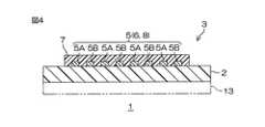
また、上記した説明では、検知部3における電極5を、1対の電極5(第1電極5Aおよび第2電極5B)として形成したが、その数は2本以上であって、電気抵抗検知器10に接続されるように偶数本であれば、特に限定されず、例えば、図4に示すように、8本、すなわち、4本の第1電極5Aと、4本の第2電極5Bとから形成することもできる。なお、図4では、各第1電極5Aおよび各第2電極5Bが、幅方向(並列)において交互に配列されている。 In the above description, the electrodes 5 in the
このように電極5を設ければ、特定のガスの種類や量(濃度)を、より一層精度よく検知することができる。
また、上記した説明では、ベース絶縁層2の下面を露出させたが、例えば、図3の仮想線で示すように、金属層13によって、ベース絶縁層2の下面を被覆することもできる。
この金属層13は、ベース絶縁層2の下に形成されており、より具体的には、ベース絶縁層2の下面全面に設けられている。If the electrode 5 is provided in this manner, the type and amount (concentration) of a specific gas can be detected with higher accuracy.
In the above description, the lower surface of the insulating
The
金属層13を形成する金属材料としては、例えば、ステンレス、42アロイ、アルミニウム、銅−ベリリウム、りん青銅などが用いられる。好ましくは、耐腐食性の観点から、ステンレスが用いられる。
この金属層13を設けるには、例えば、上記した金属層13を予め用意し、その後、ベース絶縁層2を形成する。または、金属層13およびベース絶縁層2を、金属層13およびベース絶縁層2が予め順次積層されている2層基材として用意することもできる。さらに、金属層13、ベース絶縁層2および導体層(導体パターン8を形成するための導体層)が予め順次積層されている3層基材として用意することもできる。このような3層基材としては、市販品を用いることができ、例えば、銅からなる金属層13の表面に、液晶ポリマーからなるベース絶縁層2および銅からなる導体層が予め積層されている液晶ポリマー銅張積層板(ESPANEX Lシリーズ、両面品、標準タイプ/Pタイプ、新日鐵化学社製)が用いられる。As the metal material for forming the
In order to provide the
また、金属層13の厚みは、例えば、0.05〜50μm、好ましくは、0.1〜20μmである。
このような金属層13を、ベース絶縁層2、とりわけ、ガス透過率の高い絶縁材料からなるベース絶縁層2の下に設ければ、金属層13は、下側からベース絶縁層2に接触しようとするガスを遮断できるため、雰囲気中の水蒸気の吸水によりベース絶縁層2が膨潤することを防止でき、ベース絶縁層2の下面からガスや水蒸気が透過して、導電性層7に影響を与えることを防止できる。従って、そのようなベース絶縁層2の膨潤に基づく誤検知や、ベース絶縁層2の透過の影響に基づく誤検知を、防止することができる。Moreover, the thickness of the
If such a
また、上記した説明では、導電性層7を、電極5の表面、すなわち、電極5の上面および各側面を被覆するように、形成したが、第1電極5Aおよび第2電極5Bと接続するように形成すればよく、例えば、図5に示すように、導電性層7を、電極5の各側面(保護層11の各側面)のみを被覆するように形成することもできる。なお、各検知部3において、導電性層7は、その上面が保護層11の上面と幅方向において面一となるように、形成されている。 In the above description, the
また、上記した説明では、保護層11を、導体パターン8を被覆するように形成したが、例えば、図示しないが、保護層11を、電極5のみを被覆して、検知部3の領域内に含まれない配線6を被覆しないように、形成することができる。
さらにまた、上記した説明では、保護層11を形成したが、例えば、図示しないが、保護層11を形成せず、電極5と導電性層7とを直接接触させることもできる。In the above description, the
In the above description, the
以下に実施例および比較例を示し、本発明をさらに具体的に説明するが、本発明は、何ら実施例および比較例に限定されることはない。
(センサ基板の製造)
実施例1
ベース絶縁層としての厚み25μmの液晶ポリマーシートの表面に、導体層としての厚み12μmの銅箔が予め積層されている液晶ポリマー銅張積層板(品番:ESPANEX L−12−25−00NE、片面品、標準タイプ、新日鐵化学社製)を用意し、サブトラクティブ法により、1対の電極を有する導体パターンを形成した(図3(b)参照)。なお、各電極(配線)の幅は0.25mmであり、各配線(電極)間の間隔は1.5mmであった。Hereinafter, the present invention will be described more specifically with reference to examples and comparative examples. However, the present invention is not limited to the examples and comparative examples.
(Manufacture of sensor board)
Example 1
Liquid crystal polymer copper clad laminate (product number: ESPANEX L-12-25-00NE, single-sided product) in which a 12 μm thick copper foil as a conductor layer is pre-laminated on the surface of a 25 μm thick liquid crystal polymer sheet as a base insulating layer Standard type, manufactured by Nippon Steel Chemical Co., Ltd.) was prepared, and a conductor pattern having a pair of electrodes was formed by a subtractive method (see FIG. 3B). In addition, the width | variety of each electrode (wiring) was 0.25 mm, and the space | interval between each wiring (electrode) was 1.5 mm.
次いで、厚み0.5μmの金層を、各導体パターンの表面に形成した(図3(c)参照)。
次いで、カーボンブラック(Black pearl2000)40mg、および、ポリビニルアルコール150mg、トルエン20mLを配合し、混合して、導電性成分含有液を調製した。この導電性成分含有液の25℃における粘度は、0.01Pa・sであった。Next, a gold layer having a thickness of 0.5 μm was formed on the surface of each conductor pattern (see FIG. 3C).
Next, 40 mg of carbon black (Black Pearl 2000), 150 mg of polyvinyl alcohol, and 20 mL of toluene were blended and mixed to prepare a conductive component-containing liquid. The viscosity at 25 ° C. of this conductive component-containing liquid was 0.01 Pa · s.
次いで、得られた導電性成分含有液を、超音波スプレーノズル(AccuMist Nozzle、Sono−Tec社製)を用いて、ベース絶縁層2の上に噴き付けた(図3(d)参照)。
なお、導電性成分含有液の噴き付けは、超音波の周波数を60kHzとし、25℃において、アシストガス(空気ガス、吐出圧力0.4kPa、ノズル口径約1mmφ)を導入した。また、超音波スプレーノズルの先端からベース絶縁層までの距離は、4cmとした。Next, the obtained conductive component-containing liquid was sprayed onto the insulating
The conductive component-containing liquid was sprayed with an ultrasonic frequency of 60 kHz and an assist gas (air gas, discharge pressure of 0.4 kPa, nozzle diameter of about 1 mmφ) was introduced at 25 ° C. The distance from the tip of the ultrasonic spray nozzle to the base insulating layer was 4 cm.
実施例2
超音波の周波数を120kHzとした以外は、実施例1と同様にして、センサ基板を製造した。
比較例1
導電性成分含有液を、アネスト岩田製エアブラシ(HP−CPlus)を用いて、ベース絶縁層2の上に噴き付けた以外は、実施例1と同様にして、センサ基板を製造した。Example 2
A sensor substrate was manufactured in the same manner as in Example 1 except that the frequency of the ultrasonic wave was 120 kHz.
Comparative Example 1
A sensor substrate was manufactured in the same manner as in Example 1 except that the conductive component-containing liquid was sprayed onto the
比較例2
導電性成分含有液を、公知のシリンジを用いて、ベース絶縁層2の上に滴下した以外は、実施例1と同様にして、センサ基板を製造した。
(評価)
(外観)
実施例1〜2により製造したセンサ基板では、センサ基板の表面に均一な導電性層が形成された。Comparative Example 2
A sensor substrate was produced in the same manner as in Example 1 except that the conductive component-containing liquid was dropped onto the insulating
(Evaluation)
(appearance)
In the sensor substrate manufactured according to Examples 1 and 2, a uniform conductive layer was formed on the surface of the sensor substrate.
比較例1により製造したセンサ基板では、センサ基板の表面に、カーボンブラックの凝集が確認された。
比較例2により製造したセンサ基板では、センサ基板の全面が有機溶剤によって濡れてしまい、カーボンブラックの凝集および偏在化が確認された。
(電極間の導通)
実施例1〜2により製造したセンサ基板では、安定した抵抗値を得ることができた。In the sensor substrate manufactured by Comparative Example 1, aggregation of carbon black was confirmed on the surface of the sensor substrate.
In the sensor substrate manufactured by Comparative Example 2, the entire surface of the sensor substrate was wetted by the organic solvent, and aggregation and uneven distribution of carbon black were confirmed.
(Conductivity between electrodes)
In the sensor substrate manufactured according to Examples 1 and 2, a stable resistance value could be obtained.
比較例1により製造したセンサ基板では、導通はするものの、安定した抵抗値を得ることができなかった。
比較例2により製造したセンサ基板では、ほぼ導通しなかった。
(センサ機能)
実施例1〜2により製造したセンサ基板を用いて、エタノールガスを既知濃度で含有するガス(蒸気)雰囲気に暴露させ、その雰囲気におけるエタノールガスの検知を実施した。In the sensor substrate manufactured according to Comparative Example 1, conduction was achieved, but a stable resistance value could not be obtained.
The sensor substrate manufactured according to Comparative Example 2 did not conduct substantially.
(Sensor function)
Using the sensor substrate manufactured according to Examples 1 and 2, ethanol gas was exposed to a gas (vapor) atmosphere containing a known concentration, and ethanol gas was detected in the atmosphere.
その結果、実施例1〜2のセンサ基板で、既知濃度通りのエタノールガスを検知することができた。 As a result, it was possible to detect ethanol gas at a known concentration with the sensor substrates of Examples 1 and 2.
1 センサ基板
2 ベース絶縁層
5 電極
7 導電性層1
Claims (4)
Translated fromJapanese前記絶縁層の上に、少なくとも1対の電極を形成する工程と、
前記電極を被覆するように、前記絶縁層の上に、導電性成分含有液を超音波スプレー法により噴き付けて、導電性層を形成する工程とを備え、
前記導電性成分含有液は、有機溶剤を含み、
前記超音波スプレー法では、超音波スプレー装置の噴射口を、絶縁層の上方に10〜200mmを離間した位置において、前記絶縁層に向くように設置して、前記超音波スプレー装置の前記噴射口より、前記導電性成分含有液を前記絶縁層に噴き付け、
前記超音波スプレー法を行っている間、前記導電性成分含有液の液滴が前記絶縁層に到達するまでに前記導電性成分含有液の前記有機溶剤が蒸発する
ことを特徴とする、センサ基板の製造方法。A step of preparing an insulating layer;
Forming at least one pair of electrodes on the insulating layer;
A step of spraying a conductive component-containing liquid on the insulating layer by an ultrasonic spray method so as to cover the electrode, and forming a conductive layer;
The conductive component-containing liquid contains an organic solvent,
In the ultrasonic spray method, the spray port of the ultrasonic spray device is installed at a position spaced 10 to 200 mm above the insulating layer so as to face the insulating layer, and the spray port of the ultrasonic spray device. More, spraying the conductive component-containing liquid to the insulating layer,
While performing the ultrasonic spray method, the organic solvent of the conductive component-containing liquid evaporates before the droplet of the conductive component-containing liquid reaches the insulating layer. Manufacturing method.
Priority Applications (1)
| Application Number | Priority Date | Filing Date | Title |
|---|---|---|---|
| JP2009173430AJP5315156B2 (en) | 2008-09-19 | 2009-07-24 | Manufacturing method of sensor substrate |
Applications Claiming Priority (3)
| Application Number | Priority Date | Filing Date | Title |
|---|---|---|---|
| JP2008241425 | 2008-09-19 | ||
| JP2008241425 | 2008-09-19 | ||
| JP2009173430AJP5315156B2 (en) | 2008-09-19 | 2009-07-24 | Manufacturing method of sensor substrate |
Publications (2)
| Publication Number | Publication Date |
|---|---|
| JP2010096747A JP2010096747A (en) | 2010-04-30 |
| JP5315156B2true JP5315156B2 (en) | 2013-10-16 |
Family
ID=41278393
Family Applications (1)
| Application Number | Title | Priority Date | Filing Date |
|---|---|---|---|
| JP2009173430AExpired - Fee RelatedJP5315156B2 (en) | 2008-09-19 | 2009-07-24 | Manufacturing method of sensor substrate |
Country Status (4)
| Country | Link |
|---|---|
| US (1) | US8522428B2 (en) |
| EP (1) | EP2166346B1 (en) |
| JP (1) | JP5315156B2 (en) |
| CN (1) | CN101685076A (en) |
Families Citing this family (6)
| Publication number | Priority date | Publication date | Assignee | Title |
|---|---|---|---|---|
| CN102854223A (en)* | 2012-07-30 | 2013-01-02 | 中国人民公安大学 | Black handwriting authentication instrument |
| DE102013215522A1 (en)* | 2013-08-07 | 2015-02-12 | Robert Bosch Gmbh | Sensor device for determining at least one parameter of a fluid flowing through a channel |
| DE102016217775A1 (en)* | 2016-09-16 | 2018-03-22 | Robert Bosch Gmbh | Sensor element for detecting particles of a measuring gas in a measuring gas chamber |
| CN110506202B (en)* | 2017-04-05 | 2023-02-28 | 松下控股株式会社 | gas sensor |
| JP7461340B2 (en)* | 2019-03-28 | 2024-04-03 | パナソニックホールディングス株式会社 | Gas adsorbers, gas adsorption devices and gas sensors |
| KR102853289B1 (en)* | 2022-08-08 | 2025-09-01 | 한국생산기술연구원 | Sensor for sensing nitrogen dioxide |
Family Cites Families (11)
| Publication number | Priority date | Publication date | Assignee | Title |
|---|---|---|---|---|
| JPH0337559A (en)* | 1989-07-04 | 1991-02-18 | Ryutoku Yosomiya | Ammonia sensor |
| US5725957A (en)* | 1994-07-29 | 1998-03-10 | Donnelly Corporation | Transparent substrate with diffuser surface |
| US5985356A (en)* | 1994-10-18 | 1999-11-16 | The Regents Of The University Of California | Combinatorial synthesis of novel materials |
| US5571401A (en)* | 1995-03-27 | 1996-11-05 | California Institute Of Technology | Sensor arrays for detecting analytes in fluids |
| JP3487396B2 (en)* | 1997-01-31 | 2004-01-19 | 松下電器産業株式会社 | Biosensor and manufacturing method thereof |
| US5920455A (en)* | 1997-05-01 | 1999-07-06 | Wilson Greatbatch Ltd. | One step ultrasonically coated substrate for use in a capacitor |
| JP4320069B2 (en)* | 1998-09-28 | 2009-08-26 | セイコーエプソン株式会社 | How to create a sensor device |
| JP5130616B2 (en)* | 2005-09-29 | 2013-01-30 | 凸版印刷株式会社 | Thin film forming equipment |
| EP2426552A1 (en)* | 2006-03-03 | 2012-03-07 | Gentex Corporation | Electro-optic elements incorporating improved thin-film coatings |
| US7465597B2 (en)* | 2006-06-29 | 2008-12-16 | Home Diagnostics, Inc. | Method of manufacturing a diagnostic test strip |
| JP4925835B2 (en)* | 2007-01-12 | 2012-05-09 | 日東電工株式会社 | Substance detection sensor |
- 2009
- 2009-07-24JPJP2009173430Apatent/JP5315156B2/ennot_activeExpired - Fee Related
- 2009-08-13USUS12/461,492patent/US8522428B2/ennot_activeExpired - Fee Related
- 2009-08-26EPEP09168645.1Apatent/EP2166346B1/ennot_activeNot-in-force
- 2009-09-18CNCN200910173890Apatent/CN101685076A/enactivePending
Also Published As
| Publication number | Publication date |
|---|---|
| US8522428B2 (en) | 2013-09-03 |
| JP2010096747A (en) | 2010-04-30 |
| US20100073886A1 (en) | 2010-03-25 |
| EP2166346A1 (en) | 2010-03-24 |
| CN101685076A (en) | 2010-03-31 |
| EP2166346B1 (en) | 2015-11-04 |
Similar Documents
| Publication | Publication Date | Title |
|---|---|---|
| JP2010164344A (en) | Substance detecting sensor | |
| JP4925835B2 (en) | Substance detection sensor | |
| JP5315156B2 (en) | Manufacturing method of sensor substrate | |
| US8835180B2 (en) | Organic chemical sensor comprising microporous polymer, and method of use | |
| US8227025B2 (en) | Conductive polymer coatings and methods of forming the same | |
| JP4089311B2 (en) | Conductive paste, conductive film, and method of manufacturing conductive film | |
| CN101068451B (en) | Wired circuit board | |
| JP7487104B2 (en) | Annealed metal nanoparticle decorated nanotubes | |
| TW200818562A (en) | Method for manufacturing a parts of electric circuit | |
| JP2003152383A (en) | Printed circuit board | |
| TW202206285A (en) | Member of gas sensor and method for manufacturing the member of gas sensor, gas sensor, method for gas detection and method for trace gas detection | |
| JP5178614B2 (en) | Substance detection sensor | |
| JP5007211B2 (en) | Manufacturing method of substance detection sensor | |
| JP5995662B2 (en) | Patterned plating | |
| RU2291598C2 (en) | Method for making flexible multi-layer electronic boards | |
| Godovski et al. | Absorption induced response of electrophysical characteristics of filled polymer-composite | |
| Gaidarzhi et al. | Fully printed polymer capacitive gas sensor for ammonia and toluene detection | |
| CN105585676A (en) | Laser printing method of flexible electronic device | |
| Inada et al. | Material Technology of Conductive Wiring for Ink-jet Print | |
| Nagasawa et al. | Silver coating by low-temperature sintering of nanoparticles | |
| JP2023108423A (en) | Laminate and manufacturing method of laminate | |
| Chu | Inkjet Printing of Flexible Circuits on Polymer Substrate | |
| JPS6215776A (en) | Film-like connector and manufacture thereof |
Legal Events
| Date | Code | Title | Description |
|---|---|---|---|
| A621 | Written request for application examination | Free format text:JAPANESE INTERMEDIATE CODE: A621 Effective date:20111202 | |
| A977 | Report on retrieval | Free format text:JAPANESE INTERMEDIATE CODE: A971007 Effective date:20130123 | |
| A131 | Notification of reasons for refusal | Free format text:JAPANESE INTERMEDIATE CODE: A131 Effective date:20130212 | |
| A521 | Written amendment | Free format text:JAPANESE INTERMEDIATE CODE: A523 Effective date:20130410 | |
| A131 | Notification of reasons for refusal | Free format text:JAPANESE INTERMEDIATE CODE: A131 Effective date:20130507 | |
| A521 | Written amendment | Free format text:JAPANESE INTERMEDIATE CODE: A523 Effective date:20130612 | |
| TRDD | Decision of grant or rejection written | ||
| A01 | Written decision to grant a patent or to grant a registration (utility model) | Free format text:JAPANESE INTERMEDIATE CODE: A01 Effective date:20130702 | |
| A61 | First payment of annual fees (during grant procedure) | Free format text:JAPANESE INTERMEDIATE CODE: A61 Effective date:20130708 | |
| R150 | Certificate of patent or registration of utility model | Free format text:JAPANESE INTERMEDIATE CODE: R150 | |
| LAPS | Cancellation because of no payment of annual fees |