JP5310552B2 - Wireless tag and manufacturing method thereof - Google Patents
Wireless tag and manufacturing method thereofDownload PDFInfo
- Publication number
- JP5310552B2 JP5310552B2JP2009524523AJP2009524523AJP5310552B2JP 5310552 B2JP5310552 B2JP 5310552B2JP 2009524523 AJP2009524523 AJP 2009524523AJP 2009524523 AJP2009524523 AJP 2009524523AJP 5310552 B2JP5310552 B2JP 5310552B2
- Authority
- JP
- Japan
- Prior art keywords
- resonator
- pattern
- wireless tag
- chip
- inductance
- Prior art date
- Legal status (The legal status is an assumption and is not a legal conclusion. Google has not performed a legal analysis and makes no representation as to the accuracy of the status listed.)
- Expired - Fee Related
Links
Images


Landscapes
- Aerials With Secondary Devices (AREA)
- Details Of Aerials (AREA)
Description
Translated fromJapanese本件は、無線タグ及びその製造方法に関する。前記無線タグは、例えば、金属に貼り付けることのできる金属対応の無線タグとして用いられる場合がある。 The present case relates to a wireless tag and a manufacturing method thereof. The wireless tag may be used as a metal-compatible wireless tag that can be attached to metal, for example.
無線通信システムの1つとして、RFID(Radio Frequency Identification)システムが知られている。このRFIDシステムは、一般に、無線タグ(RFIDタグとも呼ばれる)と、リーダライタ(RW)装置とを備え、RW装置から無線タグに対して無線通信により情報の読み書きが行なわれる。 An RFID (Radio Frequency Identification) system is known as one of radio communication systems. This RFID system generally includes a wireless tag (also referred to as an RFID tag) and a reader / writer (RW) device, and information is read from and written to the wireless tag from the RW device by wireless communication.
無線タグには、無線タグ自体が内蔵する電源により動作するタイプ(アクティブタグと呼ばれる)のものと、RW装置からの受信電波を駆動電力として動作するタイプ(パッシブタグと呼ばれる)のものとが知られている。 There are two types of wireless tags, one that operates with the power supply built into the wireless tag itself (called an active tag) and the other that operates with received radio waves from the RW device as drive power (called a passive tag). It has been.
パッシブタグを用いたRFIDシステムの場合、無線タグは、RW装置からの無線信号を駆動電力として、内蔵するICやLSI等の集積回路を動作させて、受信無線信号(制御信号)に応じた各種処理を行なう。無線タグからRW装置への送信は、前記受信無線信号の反射波を利用して行なう。即ち、この反射波にタグIDや前記各種処理の結果などの情報をのせて、RW装置への送信を行なう。 In the case of an RFID system using a passive tag, the wireless tag operates various integrated circuits such as an integrated circuit such as an IC or LSI by using a wireless signal from the RW device as driving power, in accordance with a received wireless signal (control signal). Perform processing. Transmission from the wireless tag to the RW device is performed using a reflected wave of the received wireless signal. That is, information such as the tag ID and the results of the above-mentioned various processings is put on this reflected wave and transmitted to the RW device.
なお、RFIDシステムには様々な周波数帯が利用されているが、最近では、UHF帯(860MHz〜960MHz)が注目されている。UHF帯は、既存の13.56MHz帯や2.45GHz帯に比べて長距離通信が可能である。欧州では868MHz、米国では915MHz、日本では953MHz付近の周波数を使用する。UHF帯の無線タグ(以下、単に「タグ」ともいう)の通信距離は、タグ内に用いるICチップやLSI等の集積回路の性能にもよるが、およそ3〜5mである。また、RW装置の出力は1ワット(W)程度である。 Note that various frequency bands are used in the RFID system, but recently, the UHF band (860 MHz to 960 MHz) has attracted attention. The UHF band is capable of long-distance communication compared to the existing 13.56 MHz band and 2.45 GHz band. Europe uses 868 MHz, 915 MHz in the United States, and 953 MHz in Japan. The communication distance of a UHF band wireless tag (hereinafter also simply referred to as “tag”) is approximately 3 to 5 m, depending on the performance of an integrated circuit such as an IC chip or LSI used in the tag. Further, the output of the RW device is about 1 watt (W).
なお、従来の無線タグとして、例えば、後記の特許文献1及び特許文献2に記載されたものがある。
特許文献1には、地板における所定の端辺から所定形状に切り込まれて形成された切り込み部を有し、切り込み部のみ折り返し構造にすることで、インピーダンスを下げることができ、インピーダンス変換回路などの別の回路を設けなくても、50Ωの給電線路に整合させることができ、構造を簡略化できて、コスト削減を図れる、平面アンテナが記載されている。Examples of conventional wireless tags include those described in
特許文献2には、無線タグにおいてアンテナインピーダンスを低く抑えながら、広帯域化を達成することを目的として、一対のアンテナパターンからなる平面アンテナと、その平面アンテナの給電点に接続されたICチップとを有する無線タグにおいて、平面アンテナを構成するアンテナパターンを、給電点側の端部に対し、給電点から遠い側の端部のパターン幅を大きくした面パターンとして、平面アンテナの広帯域化(89MHz幅のカバー)を達成するとともに、平面アンテナに隣接して形成する補助パターンを、線状ではなく、平面アンテナの1つのアンテナパターンと同じ面積を有する面パターンとして、アンテナインピーダンスを低く抑えることが記載されている。
ところで、ダンボールやプラスチックに貼り付けることを想定した通常のシート状の無線タグは、200MHz程度の通過帯域幅をもつため、欧州、米国、日本でのすべての使用周波数をカバーすることができる。しかしながら、金属に貼り付けることのできる金属対応のタグは、通過帯域が非常に狭く各国専用設計のものしか存在していない。 By the way, a normal sheet-like wireless tag assumed to be attached to cardboard or plastic has a pass bandwidth of about 200 MHz, and can cover all frequencies used in Europe, the United States, and Japan. However, metal-compatible tags that can be attached to metal have a very narrow passband and are only designed for each country.
例えば、図16に示すような形状の平面アンテナで、図15に示すような周波数対通信距離特性をもつ場合、中心周波数を米国(US)での使用周波数に合わせると、両サイドの欧州(EU)及び日本(JP)での使用周波数では通信距離が極端に落ちてしまう。中心周波数を欧州や日本での使用周波数に合わせた場合も、同様に、それ以外の地域での使用周波数では通信距離が極端に落ちてしまう。また、同一国で使用する場合でも、タグを曲面に貼り付けたり、タグの構成要素である誘電体基板(スペーサ基板)の誘電率(εr)や厚さ(t)が変わると、周波数特性がずれるため、通信距離が落ちてしまうことになる。 For example, in the case of a planar antenna having a shape as shown in FIG. 16 and having a frequency-to-communication distance characteristic as shown in FIG. 15, if the center frequency is adjusted to the frequency used in the United States (US), both sides of Europe (EU) ) And the use frequency in Japan (JP), the communication distance is extremely reduced. Similarly, when the center frequency is adjusted to the frequency used in Europe or Japan, the communication distance is extremely reduced at the frequency used in other regions. Even when used in the same country, if the tag is attached to a curved surface, or if the dielectric constant (εr) or thickness (t) of the dielectric substrate (spacer substrate) that is a component of the tag changes, the frequency characteristics will be As a result, the communication distance is reduced.
そのため、欧州、米国、日本での使用周波数をすべてカバーするような広帯域の周波数特性をもち、金属に貼り付けることのできるタグが望まれている。 Therefore, there is a demand for a tag that has a wide-band frequency characteristic that covers all frequencies used in Europe, the United States, and Japan, and can be attached to metal.
このような金属対応のタグには、パッチアンテナを用いることが多いが、広帯域化を図るには、例えば、大きさの異なるパッチアンテナを複数並べることが考えられる。後記の非特許文献1は、RFIDタグ用ではないが、その例を記載している。 For such metal-compatible tags, patch antennas are often used, but in order to increase the bandwidth, for example, it is conceivable to arrange a plurality of patch antennas having different sizes.
この非特許文献1によれば、パッチアンテナを同一平面に複数並べる場合、そのFig.1に示されるように、パッチアンテナ同士の干渉を防ぐために、両パッチアンテナを少なくとも半波長(0.5λ)の間隔をあけて並べる必要がある。
しかしながら、UHF帯のRFIDタグでは、半波長という間隔は約17cmに相当するから、RFIDタグとしては巨大になってしまい、実用的でない。金属対応でない通常のRFIDタグは、メーカによって様々であるが、およそ100mm×20mm程度のサイズである。これと同程度のサイズにコンパクトに収め、かつ、周波数特性を欧州、米国、日本での使用周波数のすべてをカバーできるように可能な限りフラットにしたい。 However, in the RFID tag in the UHF band, since the interval of half wavelength corresponds to about 17 cm, the RFID tag becomes huge and is not practical. Normal RFID tags that are not metal-compatible vary depending on the manufacturer, but are approximately 100 mm × 20 mm in size. We want to make it as compact as possible, and make the frequency response as flat as possible so that it can cover all the frequencies used in Europe, the United States, and Japan.
従来のように単にパッチアンテナを並べる場合は、少なくとも半波長程度の間隔をあける必要があり、両パッチアンテナを近づけすぎると、パッチアンテナ同士が干渉し合ってしまい、中心周波数付近の通信距離が極端に落ちるといった不具合が発生する。 When simply arranging patch antennas as in the past, it is necessary to leave at least a half wavelength interval. If both patch antennas are too close together, the patch antennas will interfere with each other, and the communication distance near the center frequency will be extreme. A problem such as falling off will occur.
なお、前記の特許文献1及び特許文献2に記載の技術は、いずれも、タグの貼り付け対象として金属を想定していないから、前記課題を解決することはできない。 In addition, since the technique described in
本件の目的の一つは、従来よりも広帯域の通過帯域(周波数対通信距離)特性をもつ金属対応の無線タグを提供することにある。 One of the objects of the present invention is to provide a metal-compatible wireless tag having a wider passband (frequency vs. communication distance) characteristic than before.
なお、前記目的に限らず、後述する発明を実施するための最良の形態に示す各構成により導かれる作用効果であって、従来の技術によっては得られない作用効果を奏することも他の目的の一つとして位置付けることができる。 The present invention is not limited to the above-described object, and is an operational effect derived from each configuration shown in the best mode for carrying out the invention to be described later. It can be positioned as one.
例えば、以下の無線タグを用いることができる。
(1)即ち、チップが接続されるチップ接続部と前記チップとのインピーダンス整合を調整しうるインダクタンス部とを有する第1の共振器パターンと、前記インダクタンス部を介した電磁誘導結合により給電される第2の共振器パターンと、をそなえ、前記インダクタンス部が、前記第2の共振器パターンの電源として機能し、前記第1の共振器パターンと前記第2の共振器パターンとが、前記インダクタンス部に流れる電流による電磁誘導結合によって前記第2の共振器パターンへの電磁結合給電がなされるほど近接して配置される、無線タグを用いることができる。For example, the following wireless tags can be used.
(1) That is, power is supplied by a first resonator pattern having a chip connection part to which a chip is connected and an inductance part capable of adjusting impedance matching between the chip and electromagnetic induction coupling via the inductance part. includes a second resonator pattern, wherein the inductance section,functions as a power source of the second resonator pattern,the first resonator pattern and the second resonator pattern, wherein the inductance section It is possible to usea wireless tag thatis arranged so close that electromagnetic coupling power is supplied to the second resonator pattern by electromagnetic inductive coupling caused by a current flowing through the second resonator pattern .
(2)ここで、前記第1及び第2の共振器パターンは、それぞれ、方形の導体パターンを有し、同一面において並列に設けられていてもよい。 (2) Here, each of the first and second resonator patterns may have a rectangular conductor pattern, and may be provided in parallel on the same plane.
(3)また、前記同一面は、誘電体基板の一方の面であってもよい。 (3) Further, the same surface may be one surface of the dielectric substrate.
(4)さらに、前記誘電体基板の他方の面に、反射層が設けられていてもよい。 (4) Furthermore, a reflective layer may be provided on the other surface of the dielectric substrate.
(5)また、前記インダクタンス部は、前記第1の共振器パターンの一部にスリットを設けることで形成されるのが好ましい。 (5) Moreover, it is preferable that the said inductance part is formed by providing a slit in a part of said 1st resonator pattern.
(6)さらに、前記第1及び第2の共振器パターンが互いに並行する方向の電気長は異なるのが好ましい。 (6) Furthermore, it is preferable that the electrical lengths in the directions in which the first and second resonator patterns are parallel to each other are different.
(7)例えば、前記第1の共振器パターンの、前記第2の共振器パターンと並行する方向の長さは、前記第2の共振器パターンの長さよりも長い方が好ましい。 (7) For example, the length of the first resonator pattern in the direction parallel to the second resonator pattern is preferably longer than the length of the second resonator pattern.
(8)また、前記第1及び第2の共振器パターンは、誘電体基板である樹脂製基板の一方の面に貼り付けられたシート状部材に導電性材料で形成されることとしてもよい。 (8) Further, the first and second resonator patterns may be formed of a conductive material on a sheet-like member attached to one surface of a resin substrate that is a dielectric substrate.
(9)さらに、前記無線タグは、前記第1及び第2の共振器パターンを被覆する樹脂材が設けられることとしてもよい。 (9) Furthermore, the wireless tag may be provided with a resin material that covers the first and second resonator patterns.
(10)また、前記チップ接続部に、前記チップが接続されていてもよい。 (10) The chip may be connected to the chip connecting portion.
(11)さらに、前記第1及び第2の共振器パターンは、誘電体を介して金属に貼り付けられることとしてもよい。 (11) Furthermore, the first and second resonator patterns may be attached to a metal via a dielectric.
(12)また、チップが接続されるチップ接続部と前記チップとのインピーダンス整合を調整しうるインダクタンス部とを有する第1の共振器パターンと、前記インダクタンス部を介した電磁誘導結合により給電される第2の共振器パターンと、をそなえ、前記第1及び第2の共振器パターンは、それぞれ、方形の導体パターンを有し、誘電体基板の一方の同一面において並列に設けられており、前記誘電体基板の他方の面の、前記第1及び第2の共振器パターンと対向する領域を含む部分に、導体パターンが設けられるとともに、前記導体パターンと、前記第1及び第2の共振器パターンとが、前記誘電体基板の一方の側面を経由する経路で電気的に接続された、無線タグを用いることができる。(12)Power is alsosupplied by a first resonator pattern having a chip connection part to which a chip is connected and an inductance part capable of adjusting impedance matching between the chip and electromagnetic induction coupling via the inductance part. Each of the first and second resonator patterns has a rectangular conductor pattern, and is provided in parallel on one same surface of the dielectric substrate, A conductor pattern is provided on a portion of the other surface of the dielectric substrate that includes a region facing the first and second resonator patterns, and the conductor pattern and the first and second resonator patterns are provided.Can be used asa wireless tag that is electrically connected through a path passing through one side surface of the dielectric substrate.
(13)さらに、前記一方の側面に、前記導体パターンと前記第1及び第2の共振器パターンとを電気的に接続する側面導体が設けられてもよい。 (13) Furthermore, a side conductor that electrically connects the conductor pattern and the first and second resonator patterns may be provided on the one side surface.
(14)また、前記側面導体は、金属メッキ又は導電性のシート状部材であってもよい。 (14) The side conductor may be a metal plating or a conductive sheet-like member.
(15)さらに、前記側面導体は、前記導体パターンと前記第1及び第2の共振器パターンとの一方又は双方と一体形成されてもよい。 (15) Furthermore, the side conductor may be integrally formed with one or both of the conductor pattern and the first and second resonator patterns.
(16)また、前記導体パターンは、前記第1及び第2の共振器パターンに共通の共振器パターンであってもよい。 (16) The conductor pattern may be a resonator pattern common to the first and second resonator patterns.
(17)さらに、前記インダクタンス部を介した電磁誘導結合により給電される第3の共振器パターンをさらにそなえ、前記第1及び第2の共振器パターンを含む面において、前記第2及び第3の共振器パターンは、前記第1の共振器パターンを中心とした対称な位置に設けられていてもよい。 (17) Further, a third resonator pattern fed by electromagnetic induction coupling via the inductance section is further provided, and the second and third resonator patterns are provided on the surface including the first and second resonator patterns. The resonator pattern may be provided at a symmetrical position around the first resonator pattern.
(18)また、前記第3の共振器パターンは、前記第1及び第2の共振器パターンの電気長よりも短い電気長を有する、こととしてもよい。 (18) Further, the third resonator pattern may have an electrical length shorter than that of the first and second resonator patterns.
(19)さらに、前記第1及び第2の共振器パターンと前記導体パターンとを全体的に被覆する樹脂材が設けられてもよい。 (19) Furthermore, a resin material that covers the first and second resonator patterns and the conductor pattern as a whole may be provided.
(20)また、無線タグの製造方法として、誘電体基板の長手方向の周囲長を定める4つの面のうち前記長手方向に対向する前記誘電体基板の側面の一方を除いた3つの面を被覆可能なシート状部材の、前記誘電体基板の一方の面及び側面に相当する領域に、チップが接続されるチップ接続部と前記チップとのインピーダンス整合を調整しうるインダクタンス部とを有する第1の共振器パターンと、前記インダクタンス部を介した電磁誘導結合により給電される第2の共振器パターンと、を形成するとともに、前記シート状部材の前記誘電体基板の他方の面に相当する領域に、前記各共振器パターンと電気的に連通する導体パターンを形成する工程と、前記第1及び第2の共振器パターンが前記誘電体基板の一方の面に位置し、前記導体パターンが前記誘電体基板の他方の面に位置するように、前記シート状部材を前記誘電体基板に巻きつけて固定する工程と、を用いることができる。 (20) Further, as a method for manufacturing a wireless tag, three surfaces except for one of the side surfaces of the dielectric substrate facing the longitudinal direction are covered among the four surfaces defining the peripheral length in the longitudinal direction of the dielectric substrate. A first sheet-like member having a chip connecting portion to which a chip is connected and an inductance portion capable of adjusting impedance matching between the chip in a region corresponding to one surface and a side surface of the dielectric substrate. In a region corresponding to the other surface of the dielectric substrate of the sheet-shaped member, a resonator pattern and a second resonator pattern fed by electromagnetic induction coupling via the inductance portion are formed. A step of forming a conductor pattern in electrical communication with each resonator pattern; and the first and second resonator patterns are located on one surface of the dielectric substrate, and the conductor pattern As emissions are positioned on the other surface of the dielectric substrate, and fixing by winding the sheet-like member to the dielectric substrate, it can be used.
(21)ここで、前記誘電体基板に、前記巻きつけ時の前記シート状部材の位置決め用ガイド部材が設けられていてもよい。 (21) Here, a guide member for positioning the sheet-like member at the time of winding may be provided on the dielectric substrate.
前記本発明によれば、従来よりも広帯域の通過帯域(周波数対通信距離)特性をもつ金属対応の無線タグを実現することができる。
また、前記無線タグをコンパクトに実現することも可能である。According to the present invention, it is possible to realize a metal-compatible wireless tag having a wider passband (frequency vs. communication distance) characteristic than before.
Further, the wireless tag can be realized in a compact manner.
1,100 誘電体スペーサ(誘電体基板)
2,200 アンテナパターン
20 アンテナパターンシート
20A 導体パターンシート
21,201 第1の導体パターン(共振器パターン)
22,202 第2の導体パターン(共振器パターン)
23 ウレタン樹脂シート(シート状樹脂材)
24,203 第3の導体パターン(共振器パターン)
204,205,206 側面導体
211 チップ接続部(給電点)
212 インダクタンス部
3 反射層(reflector)
30 反射シート(シート状反射部材)
4 金属(metal)
110 ガイド(位置決め部材)
300 導体パターン(共振器パターン)
600 樹脂(保護部材)1,100 Dielectric spacer (dielectric substrate)
2,200
22, 202 Second conductor pattern (resonator pattern)
23 Urethane resin sheet (sheet-shaped resin material)
24, 203 Third conductor pattern (resonator pattern)
204, 205, 206
212
30 Reflective sheet (sheet-like reflective member)
4 metal
110 Guide (positioning member)
300 Conductor pattern (resonator pattern)
600 Resin (protective member)
〔A〕一実施形態
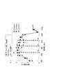
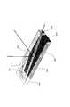
図1は、一実施形態に係る無線タグの構成を示す模式的斜視図で、この図1に示す無線タグは、金属(metal)4に貼り付けられることを想定しており、厚さt=5mm,比誘電率εr=4,誘電正接tanδ=0.001の平板状の誘電体スペーサ(誘電体基板)1の一方の面(図1における表面)にアンテナパターン2(21,22)が形成されている。[A] One Embodiment FIG. 1 is a schematic perspective view showing a configuration of a wireless tag according to one embodiment. The wireless tag shown in FIG. 1 is assumed to be attached to a
誘電体スペーサ(以下、単に「スペーサ」ともいう)1の他方の面(図1における裏面)には、無線タグの貼付対象物が非金属の場合でも同等の特性を維持できるように、金属製の反射部材(reflecter)3を設けるのが好ましい。もっとも、当該反射部材3は設けないこととすることもできる。 The other surface (the back surface in FIG. 1) of the dielectric spacer (hereinafter also simply referred to as “spacer”) 1 is made of metal so that the same characteristics can be maintained even when the object to be attached to the wireless tag is non-metallic. It is preferable to provide a
アンテナパターン2は、図1のX軸方向の長さL1=90mmの帯状(方形)の第1の導体パターン21と、X軸方向の長さL2=86mmの帯状(方形)の第2の導体パターン22とを具備し、両者はスペーサ1上で図1のY軸方向に2mmの間隔をあけて設けられている。
第1の導体パターン21は、共振周波数f1の共振器パターンとして機能し、第2の導体パターン22は、共振周波数f1よりも大きい共振周波数f2の共振器パターンとして機能する。また、アンテナパターン2のY軸方向の長さ(幅)は前記2mmの間隔を含めて27mmである。したがって、図1に示すスペーサ1のサイズは、少なくとも長さ90mm×幅27mm×厚さ(t)5mmである。The
The
ここで、無線タグにおけるアンテナパターン2は、無線タグ内に用いられる、ICチップやLSI等の集積回路(以下、チップともいう)とインピーダンス整合する必要がある。チップは、例えば図6の右側に示すように、並列のキャパシタンス成分Ccpと、並列の抵抗成分Rcpとで表すことができる。その値はメーカによって異なるが、Ccp=1pF(ピコファラド)前後、Rcp=200Ω〜20000Ωである。 Here, the
したがって、このチップと整合するようなアンテナ等価回路は、図6の左側に示すように、キャパシタンス成分Ccpと共振する並列インダクタンス成分Lapと、抵抗成分Rcpと同程度の並列抵抗Rapとで表すことができる。 Therefore, as shown on the left side of FIG. 6, an antenna equivalent circuit that matches this chip can be represented by a parallel inductance component Lap that resonates with the capacitance component Ccp and a parallel resistance Rap that is comparable to the resistance component Rcp. it can.
すなわち、アンテナパターン2は、インダクタンス成分Lapと放射抵抗成分Rapとをもつ必要がある。なお、このことは、金属対応の無線タグに限らず、RFIDの無線タグすべてに共通のことである。 That is, the
そのため、第1の共振器パターン21には、ICチップやLSI等の集積回路(以下、チップともいう)が接続されるチップ接続部(給電点)211と、インダクタンス部212とが形成されている。 Therefore, the
このインダクタンス部212は、第1の共振器パターン21の一部に、X軸方向の長さS2のスリット(Y軸方向の長さ(幅)は図1では2mm)を形成することで構成すると省スペース化を図ることができるので、望ましい。もっとも、スリットを設ける代わりにチップ接続部211からループ状線路を設ける等、他の方法により同等のインダクタンス成分を第1の共振器パターンの一部に付与(形成)してもよい。 The
なお、前記スリットの全長(ループ長)を変えることでインダクタンス値を調整できる。つまり、チップインピーダンスとの整合を調整できる。例えば、前記インダクタンス長S2を長くすればインダクタンスが大きくなる。 The inductance value can be adjusted by changing the overall length (loop length) of the slit. That is, matching with chip impedance can be adjusted. For example, increasing the inductance length S2 increases the inductance.
さらに、第1の共振器パターン21は、インダクタンス部212を含んでいるので、異なる共振周波数f1,f2(f1<f2)を得るには、第2の共振器パターン22よりもX軸方向の長さを長くした方が望ましい。その際、スペーサ1の誘電率を部分的に変えて第1の共振器パターン21の電気長の方が長くなるようにしてもよい。 Furthermore, since the
上述のごとく構成された無線タグでは、第1の共振器パターン21におけるインダクタンス部212が、以下の3つの役割を果たす。
(1)チップとの整合用インダクタンス
(2)第1の共振器パターン21への直接給電
(3)第2の共振器パターン22への電磁結合給電In the wireless tag configured as described above, the
(1) Inductance for matching with chip (2) Direct power supply to first resonator pattern 21 (3) Electromagnetic coupling power supply to
例えば図7に示すように、給電点211から第1の共振器パターン21に給電されると、インダクタンス部212には、矢印で示すように電流が非常に多く流れる(インダクタンス部212の電流分布が密になる)から、第2の共振器パターン22にとって、この部分(インダクタンス部212)は電源として働くことになる。即ち、インダクタンス部212と第2の共振器パターン22とは直接は接続されていない(2mmの間隔があいている)が、電磁誘導結合するから、インダクタンス部212を介して電磁結合給電されることになる。 For example, as shown in FIG. 7, when power is supplied from the
従来、パッチアンテナ同士をこのように間隔2mmで近接配置することは、互いに干渉し合い、アンテナ性能を劣化させるので、タブーとされてきたが、このようにインダクタンス部212による電磁誘導結合を利用することで、インダクタンス部212は第2の共振器パターン22への電源とみることができる。 Conventionally, arranging patch antennas close to each other with a spacing of 2 mm in this manner has been regarded as a taboo because they interfere with each other and degrade the antenna performance. In this way, electromagnetic induction coupling by the
したがって、両共振器パターン21,22が離れすぎると、両者の結合度が弱くなるため、第2の共振器パターン22への給電が不十分になり電波が放射しにくくなる。 Accordingly, if the two
つまり、インダクタンス部212が第2の共振器パターン22への電源とみなせるように各共振器パターン21,22を近接配置することで、アンテナパターン2全体をコンパクトに設計することができる。 That is, the
換言すれば、インダクタンス部212(スリット)を設ける位置は、第1の共振器パターン21への直接給電と、第2の共振器パターン22への電磁結合給電とが適切に行なわれる位置であるのが好ましい。例えば、第1の共振器パターン21の長さ方向(X軸方向)の中心からずれた位置、より好ましくは、図1に示すように端部近傍に設けるのがよい。 In other words, the position where the inductance portion 212 (slit) is provided is a position where the direct feeding to the
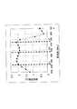
以下、本例における無線タグの特性について、3次元電磁界シミュレータを使用して計算した結果を示す。
まず、図3に、チップとアンテナパターン2の反射特性(S11)を示す。縦軸のS11は0に近いほど反射量が多く、値が小さい(マイナス)ほど整合し、アンテナパターン2の入力パワーがチップ接続部211(つまりチップ)へ伝達されやすくなることを表す。Hereinafter, the result of calculating the characteristics of the wireless tag in this example using a three-dimensional electromagnetic field simulator will be shown.
First, FIG. 3 shows the reflection characteristics (S11) of the chip and the
ここでの計算例では、チップのキャパシタンス成分Ccp=1.4pF,抵抗成分Rcp=400Ωとしている。インダクタンス長S2(ここでは、S2=20mm,23mm,25mmの3種類)によって、整合の度合いが変わるが、異なる周波数f1,f2の2共振点をもつことがわかる。 In the calculation example here, the chip capacitance component Ccp = 1.4 pF and the resistance component Rcp = 400Ω. Although the degree of matching varies depending on the inductance length S2 (here, S2 = 20 mm, 23 mm, and 25 mm), it can be seen that there are two resonance points of different frequencies f1 and f2.
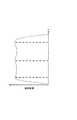
共振周波数f1,f2の値は、それぞれ、共振器パターン21の長さL1,共振器パターン22の長さL2によって制御(調整)することができる。例えば、L1を長くすれば共振周波数f1は低周波数側へ、L2を短くすれば共振周波数f2が高周波数側へ変化(シフト)する。即ち、無線タグの通過帯域幅を調整することができる。なお、アンテナゲインについては、図4に示すように、欧州、米国及び日本での各使用周波数をカバーする帯域で周波数に対してほぼ一定である。 The values of the resonance frequencies f1 and f2 can be controlled (adjusted) by the length L1 of the
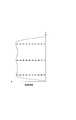
これらを総合すると、通信距離特性が計算され、図2に例示する。この図2に示すように、インダクタンス長S2=23mmとしたときが、欧州、米国及び日本での各使用周波数をカバーする帯域において最もフラットな特性を示す。なお、通信距離は図1におけるZ軸方向の通信距離であり、計算条件は、RW装置のアンテナ(RWアンテナ)が9dBiの円偏波、RWアンテナの出力27dBm(0.5W),チップの動作電力を−9dBmとしている。 When these are combined, the communication distance characteristic is calculated and is illustrated in FIG. As shown in FIG. 2, when the inductance length S2 is set to 23 mm, the flattest characteristic is shown in a band covering each use frequency in Europe, the United States, and Japan. Note that the communication distance is the communication distance in the Z-axis direction in FIG. 1. The calculation condition is that the antenna of the RW device (RW antenna) is 9 dBi of circular polarization, the output of the RW antenna is 27 dBm (0.5 W), and the operation of the chip The power is set to -9 dBm.
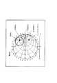
次に、図5に、使用周波数を700MHzから1200MHzまで変化させたときのスミスチャート上でのアンテナインピーダンス軌跡を示す。スミスチャート上で、チップインピーダンスに対して対称的な点(つまりチップインピーダンスの複素共役)がアンテナインピーダンスの最適点であり、この周辺にアンテナインピーダンス軌跡が小さく円を描くのが望ましい。図5では、最適点の周りにインピーダンス軌跡が2回転しているから、周波数f1(860MHz)及びf2(1000MHz)の2共振点をもつことが分かる。なお、図8に、本例のアンテナパターン2の指向性(図1におけるZY面及びZX面に関する指向性)を示す。 Next, FIG. 5 shows an antenna impedance locus on the Smith chart when the use frequency is changed from 700 MHz to 1200 MHz. On the Smith chart, a point symmetric with respect to the chip impedance (that is, the complex conjugate of the chip impedance) is the optimum point of the antenna impedance, and it is desirable that the antenna impedance locus is small and a circle is drawn around this point. In FIG. 5, since the impedance locus is rotated twice around the optimum point, it can be seen that there are two resonance points of frequency f1 (860 MHz) and f2 (1000 MHz). FIG. 8 shows the directivity of the
以上のように、本実施形態の無線タグによれば、欧州、米国及び日本での各使用周波数をカバーする広帯域な通過帯域特性をもつ金属対応の無線タグを実現できるので、各国共通で通信距離を維持可能な金属対応の無線タグを実現することができる。 As described above, according to the wireless tag of the present embodiment, it is possible to realize a metal-compatible wireless tag having a wide passband characteristic that covers each use frequency in Europe, the United States, and Japan. It is possible to realize a metal-compatible wireless tag capable of maintaining the above.
また、通過帯域特性を広帯域化できるから、例えば、無線タグをボンベ等の曲面に貼り付けたり、スペーサ1の誘電率や厚さが製造誤差により異なったりして、通過帯域の周波数特性が高周波側あるいは低周波数側にずれたとしても、欧州、米国及び日本での各使用周波数をカバーする帯域幅よりも少しでも幅広く設計しておけば、常に安定した特性(通信距離)を保つことができる。 In addition, since the passband characteristics can be broadened, for example, a wireless tag is attached to a curved surface such as a cylinder, or the dielectric constant or thickness of the
例えば図9に、製造誤差に関しての計算結果を示す。スペーサ1の誘電率εr=4.0、スペーサ1の厚さt=5mmを基準として、製造誤差により、誘電率εr=4.2となった場合や、厚さt=5.2mmとなった場合でも、欧州、米国及び日本での通信距離をほぼ一定に保つことができる。 For example, FIG. 9 shows a calculation result regarding the manufacturing error. Based on the dielectric constant εr = 4.0 of the
また、図10に、スペーサ1の幅(図1のY軸方向)(つまりはアンテナパターン2の幅)を14mmに固定して、その厚さtを3mm,4mm,5mm,10mmと変化させた場合の計算結果を示す。この図10から、厚さtを大きくするほど、欧州、米国及び日本での各使用周波数をカバーする帯域において、通信距離は伸びる傾向にあることが分かる。ただし、t=10mmでは無線タグとしては厚みがありすぎて実用的でない。逆に、t=3mm程度まで薄くすると、他に比べて通信距離は落ちるものの、実用上問題ない通信距離は確保できるから、薄型タグを実現できる。Further, in FIG. 10, the width of the spacer 1 (Y- axis direction in FIG. 1) (that is, the width of the antenna pattern 2) is fixed to 14 mm, and the thickness t is changed to 3 mm, 4 mm, 5 mm, and 10 mm. The calculation result is shown. From FIG. 10, it can be seen that the communication distance tends to increase as the thickness t increases in the band covering each frequency used in Europe, the United States, and Japan. However, when t = 10 mm, the wireless tag is too thick to be practical. On the other hand, if the thickness is reduced to about t = 3 mm, the communication distance is reduced as compared with the others, but a communication distance that is not problematic in practice can be secured, so that a thin tag can be realized.
さらに、図11に、図1に示したスペーサ1のサイズ(長さ90mm×幅27mm×厚さ(t)5mm)を基準として、スペーサ1の長さ(90mm)及び幅(27mm)を変えた場合の計算結果を示す。この図11から、幅を14mmまで小さくしても、欧州、米国及び日本での各使用周波数をカバーする帯域において通信距離の劣化は少ないことが分かる。 Further, in FIG. 11, the length (90 mm) and width (27 mm) of the
また、図12に、図1に示したスペーサ1のサイズ(長さ90mm×幅27mm×厚さ(t)5mm)を基準として、幅27mmを固定し、長さ(90mm)及び厚さt(5mm)を変化させた場合の計算結果を示す。この図12から、幅が27mmと大きいので、厚さtを薄く(3mmに)しても、欧州、米国及び日本での各使用周波数をカバーする帯域において、3m以上の通信距離を保てることが分かる。 In addition, FIG. 12 shows the size of the
以上のように、必要に応じて、スペーサ1の誘電率やサイズ(無線タグのサイズ)を変更して設計することが可能であるので、既述の寸法、スペーサ1の誘電率εr、サイズ等の値はあくまでも一例にすぎないことが理解される。 As described above, the dielectric constant and size (the size of the wireless tag) of the
(製造方法)
次に、上述した本例の無線タグは、例えば図13に模式的に示すように、フィルムや紙等のシート状部材に、銅(Cu),銀(Ag),アルミニウム(Al)等の導電性材料を印刷する等してアンテナパターン2(共振器パターン21,22)を形成したアンテナパターンシート20と、同じくフィルムや紙等のシート状部材にCu,Ag,Al等の印刷等により反射板3を形成した反射シート(シート状反射部材)30とを、ABS樹脂製のスペーサ1に、接着剤で接着あるいはラミネート加工する等の方法により一体化することで製造することができる。(Production method)
Next, the wireless tag of this example described above is electrically conductive such as copper (Cu), silver (Ag), aluminum (Al), etc. on a sheet-like member such as a film or paper as schematically shown in FIG.
また、図14に模式的に示すように、アンテナパターンシート20の両面を例えばウレタン樹脂シート(シート状樹脂材)23で覆えば、アンテナパターン2を補強ないし保護することができるから、耐環境性の向上を図ることができる。 Further, as schematically shown in FIG. 14, if both surfaces of the
なお、スペーサ1の一方の面に銅張板を設け(貼り付ける等)、当該銅張板の液体エッチングによりアンテナパターン2(共振器パターン21,22)を形成することも勿論可能である。 Of course, a copper-clad plate may be provided (attached or the like) on one surface of the
〔B〕その他
なお、前記の例では、アンテナパターン2を2つの共振器パターン21,22で構成しているが、3つ以上の共振器パターンで構成してもよい。例えば図35〜図38により後述するように、共振器パターン21,22に加えて、さらにもう1つの共振器パターン24を、例えば第1の共振器パターン21を挟んで第2の共振器パターン22の反対側へ構成して、3共振点をもつように構成することも可能である。つまり、共振器パターン数は2個に限定されないことは自明である。[B] Others In the above example, the
また、各共振器パターン21,22の形状(面パターン)は方形に限られない。例えば図39により後述するように、それぞれをクサビ状にして、互い違いに隣接配置することもできる。この場合、アンテナパターン2の幅(図1のY軸方向)をより小さくすることができる。 Further, the shape (surface pattern) of each of the
〔C〕変形例1
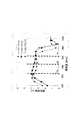
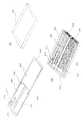
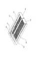
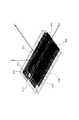
図17は、変形例1に係る無線タグを部分的に透視して示す模式的斜視図で、この図17に示す無線タグは、例示的に、誘電体スペーサ(以下、誘電体ブロックともいう)100の一方の面(図17のZ軸方向の一方の面)に、アンテナパターン200(201,202)が形成されている。また、誘電体ブロック100の他方の面には、導体パターン300が形成されている。[C]
FIG. 17 is a schematic perspective view showing the wireless tag according to the first modification partially seen through. The wireless tag shown in FIG. 17 is illustratively a dielectric spacer (hereinafter also referred to as a dielectric block). Antenna patterns 200 (201, 202) are formed on one surface 100 (one surface in the Z-axis direction in FIG. 17). A
誘電体スペーサ100には、比誘電率εr=2〜4程度の誘電体基板や樹脂を用いることができる。その一例としては、PP(ポリプロピレン)や、ABS(アクリロニトリルブタジエンスチレン)、PC(ポリカーボネイト)、PBT(ポリブチレンテレフタレート)、PPS(ポリフェニレンサルファイド)、PEEK(ポリエーテルエーテルケトン)などが挙げられる。ただし、これらに限定されない。 As the
誘電体ブロック100のサイズは、使用する周波数や比誘電率εrによって異なるが、例えば、UHF帯(860〜960MHz)、εr=3.1、誘電正接tanδ=0.001とした場合に、長さ50mm×幅30mm×厚さ(t)4mm程度である。つまり、図1に例示した無線タグに比して、X軸方向の長さが約半分のサイズとなっている。 The size of the
アンテナパターン200は、例えば誘電体ブロック100の長手方向(図17のX軸方向)に延在する帯状(方形)の第1の導体パターン201と、この第1の導体パターン201とY軸方向に隣接する帯状(方形)の第2の導体パターン202とを具備する。 The
これらの導体パターン201,202は、電磁誘導結合が容易に可能となるように配置するのが好ましい。一例として、図17において、導体パターン201,202は、誘電体ブロック100上で、図17のY軸方向に例えば3mmの間隔をあけて平行に設けられている。第1の導体パターン201のX軸方向の長さL1は例えば45mmであり、第2の導体パターン202のX軸方向の長さL2は例えば43mmである。 These
そして、本例において、第1の導体パターン201は、共振周波数f1の共振器パターンとして機能し、第2の導体パターン202は、共振周波数f1よりも大きい共振周波数f2の共振器パターンとして機能する。また、アンテナパターン200のY軸方向の長さ(幅)は前記3mmの間隔を含めて例えば27mmである。 In this example, the
導体パターン300は、例示的に、第1の共振器パターン201及び第2の共振器パターン202の面積以上で、且つ、誘電体ブロック100のXY平面における面積以下の面積を有する。例えば、導体パターン300は、アンテナパターン200全体を覆う程度のサイズ、例えば45mm×27mm程度の面積を有し、第1の共振器パターン201と第2の共振器パターン202とに共通の共振器パターンとして機能する。なお、第1の共振器パターン201は第1共振器201、第2の共振器パターン202は第2共振器202、共振器パターン300は共通共振器300とそれぞれ表記することもある。 The
そのため、第1及び第2共振器201,202は、それぞれ、誘電体ブロック100の一方の側面に設けられた導体パターン(側面導体)204及び205によって、共通共振器300と電気的に接続されている。すなわち、共通共振器(導体パターン)300と、第1及び第2共振器201,202とが、誘電体ブロック100の一方の側面を経由する経路で電気的に接続されている。 Therefore, the first and
換言すれば、誘電体ブロック100の前記他方の面(裏面)の共通共振器300から誘電体ブロック100の長手方向の一方の側面を経由して前記一方の面(表面)へ、2つの帯状の導体パターン201,202(側面導体204,205を含む)が延在する。かかる無線タグを側面(Y軸方向)から観察すると、誘電体ブロック100の長手方向の一方の側面を残して導体パターンがループ(ハーフループ)状に誘電体ブロック100に存在していることが理解される。 In other words, two band-like shapes are formed from the
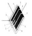
したがって、誘電体ブロック100に形成された、これらの導体パターン201〜205を展開して示すと、図23や図24の(1)に示すような形状を有する。なお、側面導体204及び205は、共振器パターン201,202と導体パターン300との一方又は双方と一体的に形成されてもよい。また、導体パターン201〜205は、例示的に、それぞれ、金メッキや、銅メッキにより形成することができる。また、側面導体204,205には、例示的に、銅やアルミニウム製の導電性テープ(シート状部材)を用いることもできる。 Therefore, when these
本例においても、無線タグにおけるアンテナパターン200は、無線タグ内に用いられる、ICチップやLSI等の集積回路(以下、チップともいう)とインピーダンス整合する。チップは、図6に例示したように、並列のキャパシタンス成分Ccpと、並列の抵抗成分Rcpとで表すことができる。例示的に、Ccp=1pF(ピコファラド)前後(例えば、1.4pF)、Rcp=200Ω〜20000Ω(例えば、400Ω)である。 Also in this example, the
したがって、このチップと整合するようなアンテナ等価回路は、図6に例示したように、キャパシタンス成分Ccpと共振する並列インダクタンス成分Lapと、抵抗成分Rcpと同程度の並列抵抗Rapとで表すことができる。すなわち、アンテナパターン200には、インダクタンス成分Lapと放射抵抗成分Rapとを有することが要求される。 Therefore, as illustrated in FIG. 6, an antenna equivalent circuit that matches this chip can be represented by a parallel inductance component Lap that resonates with the capacitance component Ccp and a parallel resistance Rap that is comparable to the resistance component Rcp. . That is, the
そのため、第1の共振器パターン201には、前記チップが接続されるチップ接続部(給電点)211が形成されている。また、この共振器パターン201には、X軸方向に長辺(長さS2)を有するスリット部212も設けられている。このスリット部212は、インダクタンス長S2のインダクタンス部として機能する。 Therefore, the
このインダクタンス部(スリット部)212は、前記チップとインピーダンス整合できる適切なサイズに設定するとよい。例えば図22に例示するように、第2(第1)共振器202(201)、側面導体205(204)および共通共振器300の長さ(矢印500で表す電気長)が使用周波数の半波長(λ/2)となるのが好ましい。このλ/2共振長は、使用周波数fや、比誘電率εrに依存する。 The inductance part (slit part) 212 may be set to an appropriate size capable of impedance matching with the chip. For example, as illustrated in FIG. 22, the length of the second (first) resonator 202 (201), the side conductor 205 (204), and the common resonator 300 (the electrical length represented by the arrow 500) is a half wavelength of the used frequency. (Λ / 2) is preferable. This λ / 2 resonance length depends on the operating frequency f and the relative dielectric constant εr.
そして、本例においても、インダクタンス部212は、以下の3つの役割を果たす。
(1)チップとの整合用(チップのキャパシタンス成分をキャンセルする)インダクタンス
(2)第1の共振器パターン21への直接給電
(3)第2の共振器パターン22への電磁結合給電And also in this example, the
(1) Inductance for matching with chip (cancels capacitance component of chip) (2) Direct power feeding to first resonator pattern 21 (3) Electromagnetic coupling power feeding to
例えば図22に示すように、給電点211から第1の共振器パターン201に給電されると、インダクタンス部212には、矢印400で示すように電流が非常に多く流れる(インダクタンス部212の電流分布が密になる)から、インダクタンス部212は、第2の共振器パターン202にとって電源として働くことになる。即ち、インダクタンス部212と第2の共振器パターン202とは直接は接続されていないが、電磁誘導結合するから、インダクタンス部212を介して電磁的に結合して給電されることになる。 For example, as shown in FIG. 22, when power is supplied from the
したがって、共振器パターン201,202同士をこのように近接して並べても、インダクタンス部212をうまく利用することで、第1の共振器パターン201は、第2の共振器パターン202への電源とみることができる。そのため、各共振器パターン201,202の間隔が離れすぎると、電磁的結合度が弱くなり、第2の共振器パターン202への給電が不十分になり電波が放射しにくくなる。 Therefore, even if the
つまり、本例においても、インダクタンス部212が第2の共振器パターン202への電源とみなせるように各共振器パターン201,202を近接配置することで、アンテナパターン200全体をコンパクトに設計することができる。 That is, also in this example, the
故に、インダクタンス部212(スリット部)を設ける位置は、第1の共振器パターン201への直接給電と、第2の共振器パターン202への電磁結合給電とが適切に行なわれる位置であるのが好ましい。例えば、第1の共振器パターン201の長さ方向(X軸方向)の中心からずれた位置、より好ましくは、図17に例示するように端部近傍に設ける。 Therefore, the position where the inductance part 212 (slit part) is provided is a position where the direct feeding to the
以下、上述した変形例1の無線タグの特性について、3次元電磁界シミュレータを使用して計算(シミュレーション)した結果の一例を示す。なお、本シミュレーションにおいて、インダクタンス部212のサイズは、X軸方向のインダクタンス長S2=18mm×Y軸方向のインダクタンス幅=2.5mmとした。 Hereinafter, an example of the result of calculation (simulation) using the three-dimensional electromagnetic simulator for the characteristics of the wireless tag of
まず、図21に、チップとアンテナパターン200の反射特性(S11)を例示する。縦軸のS11は0に近いほど反射量が多く、値が小さい(マイナス)ほど整合し、アンテナパターン200の入力パワーがチップ接続部211(つまりチップ)へ伝達されやすくなることを表す。 First, FIG. 21 illustrates the reflection characteristics (S11) of the chip and the
ここでの計算例では、チップのキャパシタンス成分Ccp=1.4pF,抵抗成分Rcp=400Ωとしている。インダクタンス長S2によって整合の度合いが変わるが、異なる周波数f1,f2の2共振点をもつことがわかる。 In the calculation example here, the chip capacitance component Ccp = 1.4 pF and the resistance component Rcp = 400Ω. Although the degree of matching varies depending on the inductance length S2, it can be seen that there are two resonance points of different frequencies f1 and f2.
共振周波数f1,f2の値は、それぞれ、共振器パターン201の長さL1,共振器パターン202の長さL2によって制御(調整)することができる。例えば、L1を長くすれば共振周波数f1は低周波数側へ、L2を短くすれば共振周波数f2が高周波数側へ変化(シフト)させることができる。即ち、無線タグの通過帯域幅を調整することができる。The values of the resonance frequencies f1 and f2 can be controlled (adjusted) by the length L1 of the
アンテナゲインについては、図20に例示するように、欧州(EU)、米国(US)及び日本(JP)での各使用周波数、例えば、EU=868MHz、US=915MHz、JP=953MHzを含む帯域で周波数に対して実用上問題ない範囲に収めることができる。 Regarding the antenna gain, as illustrated in FIG. 20, in each band used in Europe (EU), the United States (US), and Japan (JP), for example, a band including EU = 868 MHz, US = 915 MHz, and JP = 953 MHz. The frequency can be within a practically acceptable range.
これらを総合すると、通信距離(read range)特性が計算される。その一例を図19に示す。この図19に例示するように、EU、US及びJPでの各使用周波数を含む帯域において実用上問題の無い通信距離特性を得ることができる。なお、ここでの通信距離は、図17におけるZ軸方向の通信距離を意味する。計算条件は、RW装置のアンテナ(RWアンテナ)が9dBiの円偏波、RWアンテナの出力27dBm(0.5W),チップの動作電力を−9dBmとしている。 When these are combined, a communication range (read range) characteristic is calculated. An example is shown in FIG. As illustrated in FIG. 19, it is possible to obtain a communication distance characteristic having no practical problem in a band including each use frequency in EU, US, and JP. The communication distance here means the communication distance in the Z-axis direction in FIG. The calculation conditions are that the antenna of the RW device (RW antenna) is 9 dBi of circular polarization, the output of the RW antenna is 27 dBm (0.5 W), and the operating power of the chip is −9 dBm.
次に、図18に、使用周波数を700MHzから1200MHzまで変化させたときのスミスチャート上でのアンテナインピーダンス軌跡を示す。スミスチャート上で、チップインピーダンスに対して対称的な点(つまりチップインピーダンスの複素共役)がアンテナインピーダンスの最適点である。この周辺にアンテナインピーダンス軌跡が小さく円を描くのが望ましい。図18では、最適点の周りにインピーダンス軌跡が2回転しているから、2共振点をもつことが分かる。なお、図18において、fUは米国(US)における使用周波数、fEは欧州(EU)における使用周波数、fJは日本(JP)における使用周波数をそれぞれ例示している。 Next, FIG. 18 shows an antenna impedance locus on the Smith chart when the use frequency is changed from 700 MHz to 1200 MHz. On the Smith chart, a point symmetric with respect to the chip impedance (that is, a complex conjugate of the chip impedance) is the optimum point of the antenna impedance. It is desirable to draw a circle around this area with a small antenna impedance locus. In FIG. 18, since the impedance locus is rotated twice around the optimum point, it is understood that there are two resonance points. In FIG. 18, fU is a frequency used in the United States (US), fE is a frequency used in Europe (EU), and fJ is a frequency used in Japan (JP).
以上のように、本変形例の無線タグによれば、既述の実施形態と同様の作用効果が得られるほか、X軸方向の長さを約半分にすることができるから、EU,US,JPでの使用周波数を実用上問題なくカバーすることが可能な広帯域の無線タグを、さらに小型化することが可能である。 As described above, according to the wireless tag of the present modification, the same effect as that of the above-described embodiment can be obtained, and the length in the X-axis direction can be reduced to about half. It is possible to further reduce the size of a broadband wireless tag that can cover the frequency used in JP without problems in practice.
即ち、EU,US,JPのいずれの使用周波数帯域においても実用上十分な通信距離特性をもつ金属対応タグを実現することができる。したがって、曲面に貼り付けたり、誘電体ブロック100の比誘電率や厚さに誤差があったとしても、安定した通信距離特性を確保することができる。また、誘電体ブロック100の両面において半波長(λ/2)共振状態を作り出すことができるので、無線タグとして、非常にコンパクトである。That is, it is possible to realize a metal-compatible tag having practically sufficient communication distance characteristics in any of the use frequency bands of EU, US, and JP. Therefore, even if there is an error in the relative permittivity and thickness of the
(製造方法)
上述した変形例1の無線タグは、例えば図23に例示するようにして製造することができる。図23の(1)に例示するように、フィルムや紙等のシート状部材(導体パターンシート)20Aに、銅(Cu),銀(Ag),アルミニウム(Al)等の導電性材料を印刷する等して、導体パターン201,202,300を形成する。(Production method)
The wireless tag of
ここで、シート状部材20Aは、例示的に、誘電体ブロック100の長手方向(X軸方向)の周囲長を定める4つの面のうち前記長手方向に対向する誘電体ブロック100の側面の一方を除いた3つの面を被覆可能なサイズを有する。 Here, the sheet-
そして、シート状部材20Aの前記3つの面のうちの対向する一方の面及び側面に相当する領域に、導体パターン201(チップ接続部211及びインダクタンス部212)と、導体パターン202とが形成される。一方、シート状部材20Aの誘電体ブロック100の他方の面(3つの面のうちの残りの面)に相当する領域に、各共振器201,202と電気的に連通する導体パターン300が形成される。 Then, a conductor pattern 201 (a
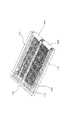
これらの導体パターン201,202,300を形成したシート状部材20Aを、図23の(2)に例示するプラスチック等の誘電体ブロック100に、巻きつけるようにして接着する。この場合、導体パターン201及び202の一部がそれぞれ誘電体ブロック100の側面に位置するように位置合わせする。これにより、前記一部が側面導体204及び205として機能し、図23の(3)に例示するように、上述した変形例1の無線タグを製造することができる。 The sheet-
なお、図24の(2)に例示するように、誘電体ブロック100には、ガイド(位置決め部材)110を設けてもよい。これによれば、前記巻きつけ時の導体パターンシート20Aの誘電体ブロック100に対する位置合わせを容易にする(位置ずれを防止する)ことができる。ガイド110は、誘電体ブロック100の表面を、導体パターンシート20Aのサイズに応じて削る等して、形成することもできるし、誘電体ブロック100の周縁にガイド110となる部材を個別に設けることで形成することもできる。 Note that, as illustrated in (2) of FIG. 24, the
図23や図24に例示するような製法によれば、変形例1の無線タグをより容易に製造することが可能であり、短期間に安価な無線タグを大量に製造することも可能となる。 According to the manufacturing method illustrated in FIG. 23 and FIG. 24, the wireless tag of
誘電体ブロック100の両面及び一方の側面にそれぞれ銅張板を設け(貼り付ける等)、銅張板の液体エッチングにより各導体パターン201,202,204,205及び300のいずれか1又は複数(全部も含む)を個別に形成することも可能である。また、側面導体204及び205のいずれか一方又は双方は、金属メッキ、あるいは、図25や図27に例示するように導電性テープとして、導体パターン201(204)及び202(205)と電気的に接続するようにしてもよい。A copper-clad plate is provided (attached or the like) on each of both surfaces and one side surface of the
また、図26に例示するように、無線タグ(各共振器201,202,300)全体(ただし、一部でもよい)を樹脂600で覆って保護するようにしてもよい。これによれば、無線タグに対する外力による損傷や、無線タグを取り付ける対象の損傷などを防止して、耐環境性を向上することが可能となる。In addition, as illustrated in FIG. 26, the entire wireless tag (
なお、樹脂600には、例えば、PP(ポリプロピレン)や、ABS(アクリロニトリルブタジエンスチレン)、PC(ポリカーボネイト)、PBT(ポリブチレンテレフタレート)、PPS(ポリフェニレンサルファイド)、PEEK(ポリエーテルエーテルケトン)などを用いることができる。 As the resin 600, for example, PP (polypropylene), ABS (acrylonitrile butadiene styrene), PC (polycarbonate), PBT (polybutylene terephthalate), PPS (polyphenylene sulfide), PEEK (polyether ether ketone), or the like is used. be able to.
〔D〕変形例2
上述した共振器パターン201,202,300は、必ずしも誘電体ブロック100の表面において四角形状を有していなくてもよい。例えば図28に例示するように、誘電体ブロック100の長辺と平行な方向から所定角度だけずれた方向をX軸とし、このX軸方向と平行な方向に、第1及び第2の共振器パターン201,202が延在するようにしてもよい。[D]
The above-described
これは、図23や図24にて説明した製造方法において、導体パターンシート20Aを誘電体ブロック100に巻きつける際に、誘電体ブロック100の長辺と非平行な方向にずらして巻きつけて、余分な導体パターン201,202,300をカットしたものに相当する。図28の例では、共振器パターン202は三角形状となっている。 This is because, in the manufacturing method described with reference to FIGS. 23 and 24, when the
また、インダクタンス部211は、スリット形状に限定されない。例えば図29に例示するように、給電線213を延長してチップ(チップ接続部211)に接続するようなインダクタンス形状としてもよい。さらには、図29及び図30に例示するように、チップ接続部211は、第2共振器202に近い側に設けてもよい。これによれば、一定の厚みの生じるチップ搭載部分を無線タグの中央側に位置させることができ、例えば、アンテナロール製造時におけるロールのバランスが良いというメリットが得られる。 Moreover, the
また、図31に例示するように、誘電体ブロック100の一方の面には、第1の共振器パターン201を挟むように第3の共振器パターン(第3共振器)203を追加的に設けてもよい。その際、第1の共振器パターン201を中心とした対称な位置に、第2及び第3共振器202,203を設けるのが好ましい。第3共振器203も、側面導体206により誘電体ブロック100の他方の面に設けられた共通共振器300と電気的に接続される。 Further, as illustrated in FIG. 31, a third resonator pattern (third resonator) 203 is additionally provided on one surface of the
つまり、誘電体ブロック100の他方の面(裏面)における共通共振器300から誘電体ブロック100の一方の側面を経由して一方の面(表面)へ、3つの帯状の共振器パターン201,202,203(側面導体204〜206を含む)が延在する。 That is, three band-
この場合の無線タグには、図32の周波数対通信距離特性に例示するように、3つの共振器201〜203に応じた3つの共振周波数f1,f2,f3をもたせることができる。したがって、利用可能な周波数帯域の拡大化を図ることができる。 In this case, the wireless tag can have three resonance frequencies f1, f2, and f3 corresponding to the three
また、図33に例示するように、X軸方向において、第3共振器203の長さは、他の共振器201,202の長さとは異なる長さに設定してもよい。例えば、第3共振器203のX軸方向の長さ(電気長)を他の共振器201,202の長さ(電気長)よりも短く(半分程度に)設定すると、図34の周波数対通信距離特性に例示するように、UHF帯と2.45GHz帯の双方に対応可能な無線タグを実現することも可能である。つまり、第3共振器203の長さを調整することで、無線タグの使用周波数を調整することが可能となる。 33, the length of the
なお、図31〜図34に例示した変形(第3共振器の付加、第3共振器のX軸方向の長さ調整)は、図35〜図38に例示するように、第1実施形態の無線タグにそれぞれ適用することも可能である。ただし、図35及び図37において、24が第3の導体(共振器)パターンを示し、第1及び第2の導体パターン21,22と共にアンテナパターン2を形成する。また、図28〜図30に例示した変形を、図39〜図41に例示するように、第1実施形態の無線タグにそれぞれ適用することも可能である。The modifications illustrated in FIGS. 31 to 34 (addition of the third resonator and adjustment of the length of the third resonator in the X-axis direction) are the same as those of the first embodiment as illustrated in FIGS. It can also be applied to each wireless tag. However, in FIG. 35 and FIG. 37, 24 shows a 3rd conductor (resonator) pattern, and the
また、上述した例では、共振器パターン300を各共振器パターン201,202(又は、201〜203)に共通としたが、個別としてもよい。その場合、2つ(又は3つ)の必要な長さの帯状の導体パターンをシート状部材20Aに形成して、誘電体ブロック100の長手方向の周囲3面に巻きつけることで、より容易に無線タグを製造することが可能となる。
そして、本発明は、以下に示すように要約することができる。
(付記1) チップが接続されるチップ接続部と前記チップとのインピーダンス整合を調整しうるインダクタンス部とを有する第1の共振器パターンと、
前記インダクタンス部を介した電磁誘導結合により給電される第2の共振器パターンと、
をそなえたことを特徴とする、無線タグ。
(付記2) 前記第1及び第2の共振器パターンは、それぞれ、方形の導体パターンを有し、同一面において並列に設けられていることを特徴とする、付記1記載の無線タグ。
(付記3) 前記同一面は、誘電体基板の一方の面であることを特徴とする、付記2記載の無線タグ。
(付記4) 前記誘電体基板の他方の面に、反射層が設けられていることを特徴とする、付記3記載の無線タグ。
(付記5) 前記インダクタンス部は、前記第1の共振器パターンの一部にスリットを設けることで形成されたことを特徴とする、付記1〜4のいずれか1つに記載の無線タグ。
(付記6) 前記第1及び第2の共振器パターンが互いに並行する方向の電気長が異なることを特徴とする、付記2記載の無線タグ。
(付記7) 前記第1の共振器パターンの、前記第2の共振器パターンと並行する方向の長さが、前記第2の共振器パターンの長さよりも長いことを特徴とする、付記6記載の無線タグ。
(付記8) 前記第1及び第2の共振器パターンは、誘電体基板である樹脂製基板の一方の面に貼り付けられたシート状部材に導電性材料で形成されたことを特徴とする、付記1〜7のいずれか1つに記載の無線タグ。
(付記9) 前記第1及び第2の共振器パターンを被覆する樹脂材が設けられたことを特徴とする、付記1〜8のいずれか1つに記載の無線タグ。
(付記10) 前記チップ接続部に、前記チップが接続されたことを特徴とする、付記1〜9のいずれか1つに記載の無線タグ。
(付記11) 前記第1及び第2の共振器パターンは、誘電体を介して金属に貼り付けられることを特徴とする、付記1〜10のいずれか1つに記載の無線タグ。
(付記12) 前記誘電体基板の他方の面の、前記第1及び第2の共振器パターンと対向する領域を含む部分に、導体パターンが設けられるとともに、
前記導体パターンと、前記第1及び第2の共振器パターンとが、前記誘電体基板の一方の側面を経由する経路で電気的に接続された、ことを特徴とする、付記3記載の無線タグ。
(付記13) 前記一方の側面に、前記導体パターンと前記第1及び第2の共振器パターンとを電気的に接続する側面導体が設けられた、ことを特徴とする、付記12記載の無線タグ。
(付記14) 前記側面導体は、金属メッキ又は導電性のシート状部材である、ことを特徴とする、付記13記載の無線タグ。
(付記15) 前記側面導体は、前記導体パターンと前記第1及び第2の共振器パターンとの一方又は双方と一体形成された、ことを特徴とする、付記13又は14に記載の無線タグ。
(付記16) 前記導体パターンは、前記第1及び第2の共振器パターンに共通の共振器パターンである、ことを特徴とする、付記12〜15のいずれか1つに記載の無線タグ。
(付記17) 前記インダクタンス部を介した電磁誘導結合により給電される第3の共振器パターンをさらにそなえ、
前記第1及び第2の共振器パターンを含む面において、前記第2及び第3の共振器パターンは、前記第1の共振器パターンを中心とした対称な位置に設けられた、ことを特徴とする、付記16記載の無線タグ。
(付記18) 前記第3の共振器パターンは、前記第1及び第2の共振器パターンの電気長よりも短い電気長を有する、ことを特徴とする、付記17記載の無線タグ。
(付記19) 前記第1及び第2の共振器パターンと前記導体パターンとを全体的に被覆する樹脂材が設けられた、ことを特徴とする、付記12〜18のいずれか1つに記載の無線タグ。
(付記20) 誘電体基板の長手方向の周囲長を定める4つの面のうち前記長手方向に対向する前記誘電体基板の側面の一方を除いた3つの面を被覆可能なシート状部材の、前記誘電体基板の一方の面及び側面に相当する領域に、チップが接続されるチップ接続部と前記チップとのインピーダンス整合を調整しうるインダクタンス部とを有する第1の共振器パターンと、前記インダクタンス部を介した電磁誘導結合により給電される第2の共振器パターンと、を形成するとともに、前記シート状部材の前記誘電体基板の他方の面に相当する領域に、前記各共振器パターンと電気的に連通する導体パターンを形成する工程と、
前記第1及び第2の共振器パターンが前記誘電体基板の一方の面に位置し、前記導体パターンが前記誘電体基板の他方の面に位置するように、前記シート状部材を前記誘電体基板に巻きつけて固定する工程と、
を有することを特徴とする、無線タグの製造方法。
(付記21) 前記誘電体基板に、前記巻きつけ時の前記シート状部材の位置決め用ガイド部材が設けられた、ことを特徴とする、付記20記載の無線タグの製造方法。Further, in the example described above, the
The present invention can be summarized as follows.
(Supplementary Note 1) A first resonator pattern having a chip connecting portion to which a chip is connected and an inductance portion capable of adjusting impedance matching between the chip,
A second resonator pattern fed by electromagnetic inductive coupling through the inductance section;
A wireless tag characterized by having
(Supplementary note 2) The wireless tag according to
(Supplementary note 3) The wireless tag according to
(Additional remark 4) The radio | wireless tag of
(Additional remark 5) The said inductance part was formed by providing a slit in a part of said 1st resonator pattern, The radio | wireless tag as described in any one of additional marks 1-4 characterized by the above-mentioned.
(Supplementary note 6) The wireless tag according to
(Supplementary note 7) The
(Additional remark 8) The said 1st and 2nd resonator pattern was formed with the electroconductive material in the sheet-like member affixed on one surface of the resin-made board | substrates which are dielectric substrates, It is characterized by the above-mentioned. The wireless tag according to any one of
(Supplementary note 9) The wireless tag according to any one of
(Supplementary note 10) The wireless tag according to any one of
(Supplementary note 11) The wireless tag according to any one of
(Additional remark 12) While a conductor pattern is provided in the part containing the area | region which opposes the said 1st and 2nd resonator pattern of the other surface of the said dielectric substrate,
The wireless tag according to
(Additional remark 13) The radio | wireless tag of Additional remark 12 characterized by the side conductor which electrically connects the said conductor pattern and said 1st and 2nd resonator pattern being provided in said one side surface. .
(Supplementary note 14) The wireless tag according to supplementary note 13, wherein the side conductor is a metal-plated or conductive sheet-like member.
(Supplementary note 15) The wireless tag according to
(Supplementary note 16) The wireless tag according to any one of Supplementary notes 12 to 15, wherein the conductor pattern is a resonator pattern common to the first and second resonator patterns.
(Supplementary Note 17) A third resonator pattern fed by electromagnetic induction coupling through the inductance section is further provided,
In the plane including the first and second resonator patterns, the second and third resonator patterns are provided at symmetrical positions around the first resonator pattern. The wireless tag according to appendix 16, wherein
(Supplementary note 18) The wireless tag according to supplementary note 17, wherein the third resonator pattern has an electrical length shorter than that of the first and second resonator patterns.
(Additional remark 19) The resin material which coat | covers the said 1st and 2nd resonator pattern and the said conductor pattern entirely was provided, It is any one of Additional remarks 12-18 characterized by the above-mentioned. Wireless tag.
(Supplementary Note 20) The sheet-like member capable of covering three surfaces excluding one of the side surfaces of the dielectric substrate facing the longitudinal direction among the four surfaces defining the peripheral length in the longitudinal direction of the dielectric substrate, A first resonator pattern having a chip connecting portion to which a chip is connected and an inductance portion capable of adjusting impedance matching between the chip and a region corresponding to one surface and side surface of the dielectric substrate; and the inductance portion A second resonator pattern that is fed by electromagnetic inductive coupling via the first and second resonator patterns, and a region corresponding to the other surface of the dielectric substrate of the sheet-like member. Forming a conductor pattern communicating with
The sheet-like member is placed on the dielectric substrate so that the first and second resonator patterns are located on one surface of the dielectric substrate and the conductor pattern is located on the other surface of the dielectric substrate. Wrapping around and fixing,
A method for manufacturing a wireless tag, comprising:
(Supplementary note 21) The wireless tag manufacturing method according to
以上詳述したように、上述した無線タグによれば、従来よりも広帯域の通過帯域(周波数対通信距離)特性をもつ金属対応の無線タグを提供することができるから、無線通信技術分野や、物品の生産、在庫、流通管理、POSシステム、セキュリティシステムなどの技術分野に極めて有用と考えられる。 As described above in detail, according to the above-described wireless tag, it is possible to provide a metal-compatible wireless tag having a wider passband (frequency vs. communication distance) characteristic than the conventional one. It is considered extremely useful in technical fields such as article production, inventory, distribution management, POS system, and security system.
Claims (12)
Translated fromJapanese前記インダクタンス部を介した電磁誘導結合により給電される第2の共振器パターンと、
をそなえ、
前記インダクタンス部が、前記第2の共振器パターンの電源として機能し、
前記第1の共振器パターンと前記第2の共振器パターンとが、前記インダクタンス部に流れる電流による電磁誘導結合によって前記第2の共振器パターンへの電磁結合給電がなされるほど近接して配置される、
ことを特徴とする、無線タグ。A first resonator pattern having a chip connection part to which a chip is connected and an inductance part capable of adjusting impedance matching between the chip;
A second resonator pattern fed by electromagnetic inductive coupling through the inductance section;
With
The inductance section,functions as a power source of the second resonator pattern,
The first resonator pattern and the second resonator pattern are arranged so close that electromagnetic coupling power is supplied to the second resonator pattern by electromagnetic induction coupling due to current flowing in the inductance section. The
A wireless tag characterized by that.
前記インダクタンス部を介した電磁誘導結合により給電される第2の共振器パターンと、をそなえ、
前記第1及び第2の共振器パターンは、それぞれ、方形の導体パターンを有し、誘電体基板の一方の同一面において並列に設けられており、
前記誘電体基板の他方の面の、前記第1及び第2の共振器パターンと対向する領域を含む部分に、導体パターンが設けられるとともに、
前記導体パターンと、前記第1及び第2の共振器パターンとが、前記誘電体基板の一方の側面を経由する経路で電気的に接続された、
ことを特徴とする、無線タグ。A first resonator pattern having a chip connection part to which a chip is connected and an inductance part capable of adjusting impedance matching between the chip;
A second resonator pattern fed by electromagnetic inductive coupling through the inductance section,
Each of the first and second resonator patterns has a rectangular conductor pattern, and is provided in parallel on one same surface of the dielectric substrate,
A conductor pattern is provided on a portion of the other surface of the dielectric substrate including a region facing the first and second resonator patterns,
The conductor pattern and the first and second resonator patterns are electrically connected through a path passing through one side surface of the dielectric substrate.
A wireless tag characterized by that.
前記第1及び第2の共振器パターンを含む面において、前記第2及び第3の共振器パターンは、前記第1の共振器パターンを中心とした対称な位置に設けられた、ことを特徴とする、請求項10記載の無線タグ。Further comprising a third resonator pattern fed by electromagnetic inductive coupling through the inductance section;
In the plane including the first and second resonator patterns, the second and third resonator patterns are provided at symmetrical positions around the first resonator pattern. The wireless tag according to claim 10.
前記第1及び第2の共振器パターンが前記誘電体基板の一方の面に位置し、前記導体パターンが前記誘電体基板の他方の面に位置するように、前記シート状部材を前記誘電体基板に巻きつけて固定する工程と、
を有することを特徴とする、無線タグの製造方法。A sheet-like member capable of covering three surfaces excluding one of the side surfaces of the dielectric substrate opposed to the longitudinal direction among the four surfaces defining the peripheral length in the longitudinal direction of the dielectric substrate. A first resonator pattern having a chip connection part to which a chip is connected and an inductance part capable of adjusting impedance matching between the chip and an electromagnetic wave via the inductance part in a region corresponding to one surface and the side surface A second resonator pattern fed by inductive coupling, and a conductor in electrical communication with each resonator pattern in a region corresponding to the other surface of the dielectric substrate of the sheet-like member Forming a pattern;
The sheet-like member is placed on the dielectric substrate so that the first and second resonator patterns are located on one surface of the dielectric substrate and the conductor pattern is located on the other surface of the dielectric substrate. Wrapping around and fixing,
A method for manufacturing a wireless tag, comprising:
Priority Applications (1)
| Application Number | Priority Date | Filing Date | Title |
|---|---|---|---|
| JP2009524523AJP5310552B2 (en) | 2007-07-25 | 2008-07-25 | Wireless tag and manufacturing method thereof |
Applications Claiming Priority (4)
| Application Number | Priority Date | Filing Date | Title |
|---|---|---|---|
| JPPCT/JP2007/064548 | 2007-07-25 | ||
| PCT/JP2007/064548WO2009013817A1 (en) | 2007-07-25 | 2007-07-25 | Wireless tag |
| JP2009524523AJP5310552B2 (en) | 2007-07-25 | 2008-07-25 | Wireless tag and manufacturing method thereof |
| PCT/JP2008/063408WO2009014213A1 (en) | 2007-07-25 | 2008-07-25 | Wireless tag and method for manufacturing the same |
Publications (2)
| Publication Number | Publication Date |
|---|---|
| JPWO2009014213A1 JPWO2009014213A1 (en) | 2010-10-07 |
| JP5310552B2true JP5310552B2 (en) | 2013-10-09 |
Family
ID=49529595
Family Applications (1)
| Application Number | Title | Priority Date | Filing Date |
|---|---|---|---|
| JP2009524523AExpired - Fee RelatedJP5310552B2 (en) | 2007-07-25 | 2008-07-25 | Wireless tag and manufacturing method thereof |
Country Status (1)
| Country | Link |
|---|---|
| JP (1) | JP5310552B2 (en) |
Cited By (1)
| Publication number | Priority date | Publication date | Assignee | Title |
|---|---|---|---|---|
| KR20150108689A (en)* | 2014-03-18 | 2015-09-30 | 엘에스엠트론 주식회사 | Internal unified antenna module for vehicle |
Citations (8)
| Publication number | Priority date | Publication date | Assignee | Title |
|---|---|---|---|---|
| JPH04157905A (en)* | 1990-10-22 | 1992-05-29 | Nippon Telegr & Teleph Corp <Ntt> | Broad band plane antenna |
| JPH0758539A (en)* | 1993-08-13 | 1995-03-03 | Matsushita Electric Ind Co Ltd | Microstrip antenna |
| JPH11127014A (en)* | 1997-10-23 | 1999-05-11 | Mitsubishi Materials Corp | Antenna system |
| JP2002135029A (en)* | 2000-10-25 | 2002-05-10 | Hitachi Ltd | Transponder of moving object identification device |
| JP2005198168A (en)* | 2004-01-09 | 2005-07-21 | Toppan Forms Co Ltd | Non-contact type information recording medium and label using the same |
| JP2005348197A (en)* | 2004-06-04 | 2005-12-15 | Hitachi Chem Co Ltd | Radio electronic device |
| JP2006195795A (en)* | 2005-01-14 | 2006-07-27 | Hitachi Chem Co Ltd | Ic tag inlet, and manufacturing method for ic tag inlet |
| JP2006309401A (en)* | 2005-04-27 | 2006-11-09 | Hitachi Chem Co Ltd | Ic tag |
- 2008
- 2008-07-25JPJP2009524523Apatent/JP5310552B2/ennot_activeExpired - Fee Related
Patent Citations (8)
| Publication number | Priority date | Publication date | Assignee | Title |
|---|---|---|---|---|
| JPH04157905A (en)* | 1990-10-22 | 1992-05-29 | Nippon Telegr & Teleph Corp <Ntt> | Broad band plane antenna |
| JPH0758539A (en)* | 1993-08-13 | 1995-03-03 | Matsushita Electric Ind Co Ltd | Microstrip antenna |
| JPH11127014A (en)* | 1997-10-23 | 1999-05-11 | Mitsubishi Materials Corp | Antenna system |
| JP2002135029A (en)* | 2000-10-25 | 2002-05-10 | Hitachi Ltd | Transponder of moving object identification device |
| JP2005198168A (en)* | 2004-01-09 | 2005-07-21 | Toppan Forms Co Ltd | Non-contact type information recording medium and label using the same |
| JP2005348197A (en)* | 2004-06-04 | 2005-12-15 | Hitachi Chem Co Ltd | Radio electronic device |
| JP2006195795A (en)* | 2005-01-14 | 2006-07-27 | Hitachi Chem Co Ltd | Ic tag inlet, and manufacturing method for ic tag inlet |
| JP2006309401A (en)* | 2005-04-27 | 2006-11-09 | Hitachi Chem Co Ltd | Ic tag |
Cited By (2)
| Publication number | Priority date | Publication date | Assignee | Title |
|---|---|---|---|---|
| KR20150108689A (en)* | 2014-03-18 | 2015-09-30 | 엘에스엠트론 주식회사 | Internal unified antenna module for vehicle |
| KR101945070B1 (en)* | 2014-03-18 | 2019-02-01 | 엘에스엠트론 주식회사 | Internal unified antenna module for vehicle |
Also Published As
| Publication number | Publication date |
|---|---|
| JPWO2009014213A1 (en) | 2010-10-07 |
Similar Documents
| Publication | Publication Date | Title |
|---|---|---|
| KR101070980B1 (en) | Wireless tag and method for manufacturing the same | |
| EP1887653B1 (en) | RFID tag and manufacturing method thereof | |
| EP2375493B1 (en) | Wireless IC device | |
| KR101012528B1 (en) | RFID tag | |
| JP6465109B2 (en) | Multi-antenna and radio apparatus including the same | |
| JP4498364B2 (en) | Antenna and contactless tag | |
| EP2840648B1 (en) | Wireless IC device | |
| US8952859B2 (en) | Compact antenna system having folded dipole and/or monopole | |
| EP2251933A1 (en) | Composite antenna | |
| US20080122628A1 (en) | RFID tag antenna and RFID tag | |
| AU2006346817A1 (en) | Antenna for near field and far field radio frequency identification | |
| JP2014053885A (en) | Multi-band antenna | |
| WO2007029296A1 (en) | Rf tag and method for manufacturing rf tag | |
| JP6478510B2 (en) | antenna | |
| KR101014624B1 (en) | An antenna module operating in a multiband and a communication system including the antenna module | |
| TWI418089B (en) | Radio frequency identification tag and manufacturing method thereof | |
| US20100051700A1 (en) | Radio apparatus, antenna device and radio communication system for contactless communication | |
| JP5310552B2 (en) | Wireless tag and manufacturing method thereof | |
| JP2019004266A (en) | Antenna device and electronic apparatus | |
| WO2014103025A1 (en) | Wireless ic tag apparatus | |
| JP2024126457A (en) | Hybrid IC card and IC tag | |
| JP2013012936A (en) | Antenna device |
Legal Events
| Date | Code | Title | Description |
|---|---|---|---|
| A131 | Notification of reasons for refusal | Free format text:JAPANESE INTERMEDIATE CODE: A131 Effective date:20120522 | |
| A521 | Request for written amendment filed | Free format text:JAPANESE INTERMEDIATE CODE: A523 Effective date:20120529 | |
| A131 | Notification of reasons for refusal | Free format text:JAPANESE INTERMEDIATE CODE: A131 Effective date:20121127 | |
| A521 | Request for written amendment filed | Free format text:JAPANESE INTERMEDIATE CODE: A523 Effective date:20130128 | |
| TRDD | Decision of grant or rejection written | ||
| A01 | Written decision to grant a patent or to grant a registration (utility model) | Free format text:JAPANESE INTERMEDIATE CODE: A01 Effective date:20130604 | |
| A61 | First payment of annual fees (during grant procedure) | Free format text:JAPANESE INTERMEDIATE CODE: A61 Effective date:20130617 | |
| R150 | Certificate of patent or registration of utility model | Ref document number:5310552 Country of ref document:JP Free format text:JAPANESE INTERMEDIATE CODE: R150 Free format text:JAPANESE INTERMEDIATE CODE: R150 | |
| LAPS | Cancellation because of no payment of annual fees |