JP5309885B2 - Method for manufacturing ceramic substrate for power module substrate and method for manufacturing power module substrate - Google Patents
Method for manufacturing ceramic substrate for power module substrate and method for manufacturing power module substrateDownload PDFInfo
- Publication number
- JP5309885B2 JP5309885B2JP2008271036AJP2008271036AJP5309885B2JP 5309885 B2JP5309885 B2JP 5309885B2JP 2008271036 AJP2008271036 AJP 2008271036AJP 2008271036 AJP2008271036 AJP 2008271036AJP 5309885 B2JP5309885 B2JP 5309885B2
- Authority
- JP
- Japan
- Prior art keywords
- power module
- substrate
- ceramic
- ceramic substrate
- manufacturing
- Prior art date
- Legal status (The legal status is an assumption and is not a legal conclusion. Google has not performed a legal analysis and makes no representation as to the accuracy of the status listed.)
- Active
Links
- 239000000919ceramicSubstances0.000titleclaimsdescription156
- 239000000758substrateSubstances0.000titleclaimsdescription156
- 238000000034methodMethods0.000titleclaimsdescription46
- 238000004519manufacturing processMethods0.000titleclaimsdescription37
- 229910052751metalInorganic materials0.000claimsdescription80
- 239000002184metalSubstances0.000claimsdescription79
- 239000000463materialSubstances0.000claimsdescription59
- 239000007789gasSubstances0.000claimsdescription44
- 229910052710siliconInorganic materials0.000claimsdescription33
- XUIMIQQOPSSXEZ-UHFFFAOYSA-NSiliconChemical compound[Si]XUIMIQQOPSSXEZ-UHFFFAOYSA-N0.000claimsdescription32
- 239000010703siliconSubstances0.000claimsdescription32
- 239000002131composite materialSubstances0.000claimsdescription29
- VYPSYNLAJGMNEJ-UHFFFAOYSA-NSilicium dioxideChemical compoundO=[Si]=OVYPSYNLAJGMNEJ-UHFFFAOYSA-N0.000claimsdescription28
- 229910052814silicon oxideInorganic materials0.000claimsdescription28
- 238000004441surface measurementMethods0.000claimsdescription21
- 238000001312dry etchingMethods0.000claimsdescription20
- 238000004381surface treatmentMethods0.000claimsdescription20
- 238000005245sinteringMethods0.000claimsdescription10
- 238000005219brazingMethods0.000claimsdescription9
- -1fluoride ionsChemical class0.000claimsdescription9
- 229910052782aluminiumInorganic materials0.000claimsdescription7
- 239000000523sampleSubstances0.000claimsdescription7
- XAGFODPZIPBFFR-UHFFFAOYSA-NaluminiumChemical compound[Al]XAGFODPZIPBFFR-UHFFFAOYSA-N0.000claimsdescription6
- GVGCUCJTUSOZKP-UHFFFAOYSA-Nnitrogen trifluorideChemical compoundFN(F)FGVGCUCJTUSOZKP-UHFFFAOYSA-N0.000claimsdescription6
- TXEYQDLBPFQVAA-UHFFFAOYSA-NtetrafluoromethaneChemical compoundFC(F)(F)FTXEYQDLBPFQVAA-UHFFFAOYSA-N0.000claimsdescription4
- 239000011159matrix materialSubstances0.000claims1
- LIVNPJMFVYWSIS-UHFFFAOYSA-Nsilicon monoxideChemical compound[Si-]#[O+]LIVNPJMFVYWSIS-UHFFFAOYSA-N0.000description22
- 125000004429atomChemical group0.000description16
- 229910004298SiO 2Inorganic materials0.000description9
- KRHYYFGTRYWZRS-UHFFFAOYSA-MFluoride anionChemical compound[F-]KRHYYFGTRYWZRS-UHFFFAOYSA-M0.000description8
- 238000005304joiningMethods0.000description7
- 238000006243chemical reactionMethods0.000description6
- PNEYBMLMFCGWSK-UHFFFAOYSA-Naluminium oxideInorganic materials[O-2].[O-2].[O-2].[Al+3].[Al+3]PNEYBMLMFCGWSK-UHFFFAOYSA-N0.000description5
- 239000003517fumeSubstances0.000description5
- 229910018072Al 2 O 3Inorganic materials0.000description4
- 229910016569AlF 3Inorganic materials0.000description4
- LFQSCWFLJHTTHZ-UHFFFAOYSA-NEthanolChemical compoundCCOLFQSCWFLJHTTHZ-UHFFFAOYSA-N0.000description4
- 229910017855NH 4 FInorganic materials0.000description4
- 239000012159carrier gasSubstances0.000description4
- 238000005530etchingMethods0.000description4
- 239000010931goldSubstances0.000description4
- 238000005422blastingMethods0.000description3
- PMHQVHHXPFUNSP-UHFFFAOYSA-Mcopper(1+);methylsulfanylmethane;bromideChemical compoundBr[Cu].CSCPMHQVHHXPFUNSP-UHFFFAOYSA-M0.000description3
- 230000001678irradiating effectEffects0.000description3
- 238000005259measurementMethods0.000description3
- 238000004445quantitative analysisMethods0.000description3
- 239000004065semiconductorSubstances0.000description3
- 229910010271silicon carbideInorganic materials0.000description3
- IRPGOXJVTQTAAN-UHFFFAOYSA-N2,2,3,3,3-pentafluoropropanalChemical compoundFC(F)(F)C(F)(F)C=OIRPGOXJVTQTAAN-UHFFFAOYSA-N0.000description2
- KLZUFWVZNOTSEM-UHFFFAOYSA-KAluminum fluorideInorganic materialsF[Al](F)FKLZUFWVZNOTSEM-UHFFFAOYSA-K0.000description2
- 229910018503SF6Inorganic materials0.000description2
- 229910052581Si3N4Inorganic materials0.000description2
- 229910052799carbonInorganic materials0.000description2
- 238000004140cleaningMethods0.000description2
- 239000000498cooling waterSubstances0.000description2
- 229910052802copperInorganic materials0.000description2
- 239000010949copperSubstances0.000description2
- 239000012153distilled waterSubstances0.000description2
- 238000001035dryingMethods0.000description2
- 229910052737goldInorganic materials0.000description2
- 239000001257hydrogenSubstances0.000description2
- 229910052739hydrogenInorganic materials0.000description2
- CPLXHLVBOLITMK-UHFFFAOYSA-Nmagnesium oxideInorganic materials[Mg]=OCPLXHLVBOLITMK-UHFFFAOYSA-N0.000description2
- 239000000395magnesium oxideSubstances0.000description2
- AXZKOIWUVFPNLO-UHFFFAOYSA-Nmagnesium;oxygen(2-)Chemical compound[O-2].[Mg+2]AXZKOIWUVFPNLO-UHFFFAOYSA-N0.000description2
- 238000002156mixingMethods0.000description2
- 238000001020plasma etchingMethods0.000description2
- 239000000843powderSubstances0.000description2
- HBMJWWWQQXIZIP-UHFFFAOYSA-Nsilicon carbideChemical compound[Si+]#[C-]HBMJWWWQQXIZIP-UHFFFAOYSA-N0.000description2
- HQVNEWCFYHHQES-UHFFFAOYSA-Nsilicon nitrideChemical compoundN12[Si]34N5[Si]62N3[Si]51N64HQVNEWCFYHHQES-UHFFFAOYSA-N0.000description2
- 229910000679solderInorganic materials0.000description2
- SFZCNBIFKDRMGX-UHFFFAOYSA-Nsulfur hexafluorideChemical compoundFS(F)(F)(F)(F)FSFZCNBIFKDRMGX-UHFFFAOYSA-N0.000description2
- 229960000909sulfur hexafluorideDrugs0.000description2
- 238000004506ultrasonic cleaningMethods0.000description2
- XLYOFNOQVPJJNP-UHFFFAOYSA-NwaterChemical compoundOXLYOFNOQVPJJNP-UHFFFAOYSA-N0.000description2
- 238000001039wet etchingMethods0.000description2
- OKTJSMMVPCPJKN-UHFFFAOYSA-NCarbonChemical compound[C]OKTJSMMVPCPJKN-UHFFFAOYSA-N0.000description1
- RYGMFSIKBFXOCR-UHFFFAOYSA-NCopperChemical compound[Cu]RYGMFSIKBFXOCR-UHFFFAOYSA-N0.000description1
- YCKRFDGAMUMZLT-UHFFFAOYSA-NFluorine atomChemical compound[F]YCKRFDGAMUMZLT-UHFFFAOYSA-N0.000description1
- UFHFLCQGNIYNRP-UHFFFAOYSA-NHydrogenChemical compound[H][H]UFHFLCQGNIYNRP-UHFFFAOYSA-N0.000description1
- ZOKXTWBITQBERF-UHFFFAOYSA-NMolybdenumChemical compound[Mo]ZOKXTWBITQBERF-UHFFFAOYSA-N0.000description1
- MCMNRKCIXSYSNV-UHFFFAOYSA-NZrO2Inorganic materialsO=[Zr]=OMCMNRKCIXSYSNV-UHFFFAOYSA-N0.000description1
- 230000001133accelerationEffects0.000description1
- CSDREXVUYHZDNP-UHFFFAOYSA-NalumanylidynesiliconChemical compound[Al].[Si]CSDREXVUYHZDNP-UHFFFAOYSA-N0.000description1
- QVGXLLKOCUKJST-UHFFFAOYSA-Natomic oxygenChemical group[O]QVGXLLKOCUKJST-UHFFFAOYSA-N0.000description1
- 238000005452bendingMethods0.000description1
- 230000015572biosynthetic processEffects0.000description1
- 239000002826coolantSubstances0.000description1
- 238000001816coolingMethods0.000description1
- 238000001514detection methodMethods0.000description1
- 238000010586diagramMethods0.000description1
- 230000000694effectsEffects0.000description1
- 239000011737fluorineSubstances0.000description1
- 229910052731fluorineInorganic materials0.000description1
- PCHJSUWPFVWCPO-UHFFFAOYSA-NgoldChemical compound[Au]PCHJSUWPFVWCPO-UHFFFAOYSA-N0.000description1
- 239000004519greaseSubstances0.000description1
- 238000010438heat treatmentMethods0.000description1
- 150000002431hydrogenChemical class0.000description1
- 238000010884ion-beam techniqueMethods0.000description1
- 239000007769metal materialSubstances0.000description1
- 229910052750molybdenumInorganic materials0.000description1
- 239000011733molybdenumSubstances0.000description1
- 230000003647oxidationEffects0.000description1
- 238000007254oxidation reactionMethods0.000description1
- TWNQGVIAIRXVLR-UHFFFAOYSA-Noxo(oxoalumanyloxy)alumaneChemical compoundO=[Al]O[Al]=OTWNQGVIAIRXVLR-UHFFFAOYSA-N0.000description1
- SIWVEOZUMHYXCS-UHFFFAOYSA-Noxo(oxoyttriooxy)yttriumChemical compoundO=[Y]O[Y]=OSIWVEOZUMHYXCS-UHFFFAOYSA-N0.000description1
- 229910052760oxygenInorganic materials0.000description1
- 239000001301oxygenSubstances0.000description1
- RVTZCBVAJQQJTK-UHFFFAOYSA-Noxygen(2-);zirconium(4+)Chemical compound[O-2].[O-2].[Zr+4]RVTZCBVAJQQJTK-UHFFFAOYSA-N0.000description1
- ABTOQLMXBSRXSM-UHFFFAOYSA-Nsilicon tetrafluorideChemical compoundF[Si](F)(F)FABTOQLMXBSRXSM-UHFFFAOYSA-N0.000description1
- 238000005507sprayingMethods0.000description1
- 238000005382thermal cyclingMethods0.000description1
- 238000007740vapor depositionMethods0.000description1
Images


Classifications
- H—ELECTRICITY
- H01—ELECTRIC ELEMENTS
- H01L—SEMICONDUCTOR DEVICES NOT COVERED BY CLASS H10
- H01L2224/00—Indexing scheme for arrangements for connecting or disconnecting semiconductor or solid-state bodies and methods related thereto as covered by H01L24/00
- H01L2224/01—Means for bonding being attached to, or being formed on, the surface to be connected, e.g. chip-to-package, die-attach, "first-level" interconnects; Manufacturing methods related thereto
- H01L2224/26—Layer connectors, e.g. plate connectors, solder or adhesive layers; Manufacturing methods related thereto
- H01L2224/31—Structure, shape, material or disposition of the layer connectors after the connecting process
- H01L2224/32—Structure, shape, material or disposition of the layer connectors after the connecting process of an individual layer connector
- H01L2224/321—Disposition
- H01L2224/32151—Disposition the layer connector connecting between a semiconductor or solid-state body and an item not being a semiconductor or solid-state body, e.g. chip-to-substrate, chip-to-passive
- H01L2224/32221—Disposition the layer connector connecting between a semiconductor or solid-state body and an item not being a semiconductor or solid-state body, e.g. chip-to-substrate, chip-to-passive the body and the item being stacked
- H01L2224/32225—Disposition the layer connector connecting between a semiconductor or solid-state body and an item not being a semiconductor or solid-state body, e.g. chip-to-substrate, chip-to-passive the body and the item being stacked the item being non-metallic, e.g. insulating substrate with or without metallisation
- H—ELECTRICITY
- H01—ELECTRIC ELEMENTS
- H01L—SEMICONDUCTOR DEVICES NOT COVERED BY CLASS H10
- H01L2924/00—Indexing scheme for arrangements or methods for connecting or disconnecting semiconductor or solid-state bodies as covered by H01L24/00
- H01L2924/10—Details of semiconductor or other solid state devices to be connected
- H01L2924/11—Device type
- H01L2924/13—Discrete devices, e.g. 3 terminal devices
- H01L2924/1304—Transistor
- H01L2924/1305—Bipolar Junction Transistor [BJT]
- H01L2924/13055—Insulated gate bipolar transistor [IGBT]
Landscapes
- Ceramic Products (AREA)
- Structure Of Printed Boards (AREA)
- Manufacturing Of Printed Wiring (AREA)
Description
Translated fromJapanese本発明は、Siを含有してなるセラミックス基板に金属部材が接合されてなるパワーモジュール用基板のセラミックス基板の製造方法及びこのセラミックス基板を用いたパワーモジュール用基板の製造方法に関する。The present invention relates to a method for manufacturinga ceramic substrate for a power module substrate inwhich a metal member is bonded to a ceramic substrate containing Si, and a method for manufacturing a power module substrate using the ceramic substrate.
例えば半導体チップなどの電子部品が実装されたパワーモジュールは、一般にAlN(窒化アルミニウム)やAl2O3(アルミナ)、Si3N4(窒化珪素)、SiC(シリコンカーバイド)などからなるセラミックス基板と、該セラミックス基板の上面に配置された金属部材の回路層と、該セラミックス基板の下面に配置された金属部材の金属層とを有するパワーモジュール用基板を備え、該パワーモジュール用基板の回路層上に、発熱体である半導体チップを配設し、金属層の下面には冷却用のヒートシンクを配設している(特許文献1参照)。For example, a power module on which an electronic component such as a semiconductor chip is mounted generally includes a ceramic substrate made of AlN (aluminum nitride), Al2 O3 (alumina), Si3 N4 (silicon nitride), SiC (silicon carbide), and the like. A power module substrate having a circuit layer of a metal member disposed on the upper surface of the ceramic substrate and a metal layer of a metal member disposed on the lower surface of the ceramic substrate, and on the circuit layer of the power module substrate. In addition, a semiconductor chip as a heating element is disposed, and a cooling heat sink is disposed on the lower surface of the metal layer (see Patent Document 1).
そして、パワーモジュールは、半導体チップで発生した熱を、金属層を介してヒートシンク中の冷却水へ放散させる構成となっている。
ここで、セラミックス基板としてAlNよりも高い曲げ強度を有するなど機械的特性に優れるSi3N4を用いることにより、セラミックス基板の薄肉化が図れる。
Here, the thickness of the ceramic substrate can be reduced by using Si3 N4 having excellent mechanical properties such as higher bending strength than AlN as the ceramic substrate.
しかしながら、上記従来のパワーモジュール用基板には、以下の課題が残されている。
例えば、Siを含有するSi3N4からなるセラミックス基板とAl(アルミニウム)からなる金属部材とを用いてこれらを接合させた際に、セラミックス基板と金属部材との間で接合不良が発生することがある。However, the following problems remain in the conventional power module substrate.
For example, when these are joined using a ceramic substrate made of Si3 N4 containing Si and a metal member made of Al (aluminum), poor bonding occurs between the ceramic substrate and the metal member. There is.
すなわち、セラミックス基板の接合する表面部分には、セラミックス基板を焼結した際に生じたSiO2(酸化シリコン)やシリコンの複合酸化物が存在しており、接合時において、これら酸化シリコン及びシリコンの複合酸化物に起因したSiOガスが発生し、セラミックス基板と金属部材との接合面積が充分に確保できなくなる。そして、このような接合不良により、熱サイクル時において、セラミックス基板と金属部材との剥離が生じやすくなる。That is, SiO2 (silicon oxide) or silicon composite oxide generated when the ceramic substrate is sintered is present on the surface portion to which the ceramic substrate is bonded. SiO gas resulting from the composite oxide is generated, and a sufficient bonding area between the ceramic substrate and the metal member cannot be secured. Due to such poor bonding, the ceramic substrate and the metal member are easily peeled off during the thermal cycle.
本発明は、前述の課題に鑑みてなされたもので、Siを含有してなるセラミックス基板と金属部材とを接合させた際に充分な接合強度が得られ、熱サイクル時における接合信頼性が高められるパワーモジュール用基板のセラミックス基板の製造方法及びパワーモジュール用基板の製造方法を提供することを目的としている。The present invention has been made in view of the above-mentioned problems. When a ceramic substrate containing Si and a metal member are bonded, sufficient bonding strength is obtained, and bonding reliability during thermal cycling is improved. It is an object of the present invention to provide a method for manufacturinga ceramic substrate for a power module substrate and a method for manufacturing a power module substrate.
前記目的を達成するために、本発明は以下の手段を提案している。
すなわち本発明は、セラミックス基板に金属部材が接合されてなるパワーモジュール用基板のセラミックス基板の製造方法であって、Siを含有するセラミックス母材を焼結する工程と、前記セラミックス母材の表面にフッ化物イオンを含むガスを用いてドライエッチングを施す表面処理工程と、を備え、前記表面処理工程において、前記セラミックス母材の表面のうち少なくとも前記金属部材が接合される表面部分の酸化シリコン及びシリコンの複合酸化物の濃度を電子プローブマイクロアナライザを用いた表面測定で2.7Atom%以下とすることを特徴とする。
また、本発明に係るパワーモジュール用基板の製造方法は、前述のパワーモジュール用基板のセラミックス基板の製造方法によって得られるセラミックス基板に、金属部材を接合することを特徴とする。In order to achieve the above object, the present invention proposes the following means.
That is, the present onsetMing,the metal member to the ceramic substrate is a method of manufacturing a ceramic substrate power module substrate formed by bonding, and sintering the ceramic base material containing Si, the surface of the ceramic base material A surface treatment step of performing dry etching using a gas containing fluoride ions, and in thesurface treatment step,at least a surface portion of the surface of the ceramic base material towhich the metal member is bonded and silicon oxide the concentration of the composite oxide of silicon and wherein the 2.7 Atom% or less and toTurkey the surface measurement using the electron probe microanalyzer.
The power module substrate manufacturing method according to the present invention is characterized in that a metal member is bondedto the ceramic substrateobtained by theabove-described ceramic substrate manufacturing method for a power module substrate .
本発明に係るパワーモジュール用基板のセラミックス基板の製造方法及びパワーモジュール用基板の製造方法によれば、Siを含有するセラミックス母材を焼結した後、表面に酸化シリコン及びシリコンの複合酸化物が付着した状態のセラミックス母材に、フッ化物イオンを含むガスを用いてドライエッチングが施されるので、該セラミックス母材の表面の酸化シリコン及びシリコンの複合酸化物の濃度が電子プローブマイクロアナライザを用いた表面測定で2.7Atom%以下にまで低減される。すなわち、表面処理工程において、セラミックス母材の表面の酸化シリコン及びシリコンの複合酸化物がフッ化物イオンと反応し、揮発性の高いSiF4(四フッ化珪素)ガス等となり表面から除去されるため、該表面における酸化シリコン及びシリコンの複合酸化物の濃度が前記表面測定で2.7Atom%以下にまで確実に低減されるようになっている。According to the method for manufacturinga ceramic substrate for a power module substrate and the method for manufacturing a power module substrate according to the present invention, after sintering a ceramic base material containing Si, silicon oxide and a composite oxide of silicon are formed on the surface. Since the adhering ceramic base material is dry-etched using a gas containing fluoride ions, the concentration of silicon oxide and silicon composite oxide on the surface of the ceramic base material is determined using an electronic probe microanalyzer. It is reduced to 2.7 Atom% or less by the measured surface measurement. That is, in the surface treatment process, silicon oxide and silicon composite oxide on the surface of the ceramic base material react with fluoride ions to be removed from the surface as highly volatile SiF4 (silicon tetrafluoride) gas. The concentration of silicon oxide and silicon complex oxide on the surface is reliably reduced to 2.7 Atom% or less in the surface measurement.
従って、このようにして製造されたセラミックス基板と金属部材とを接合した際に、酸化シリコン及びシリコンの複合酸化物に起因するSiO(一酸化珪素)ガスの発生が抑制されることから、セラミックス基板と金属部材との接合面積が充分に確保されるとともに、熱サイクル時におけるセラミックス基板と金属部材との剥離が防止されて、接合信頼性が高められている。 Accordingly, since the generation of SiO (silicon monoxide) gas due to the silicon oxide and the composite oxide of silicon is suppressed when the ceramic substrate thus manufactured and the metal member are joined, the ceramic substrate A sufficient bonding area between the metal member and the metal member is ensured, and the ceramic substrate and the metal member are prevented from being peeled off during the thermal cycle, thereby improving the bonding reliability.
また、ドライエッチングのガスに含まれるフッ化物イオンは、前述した反応によりSiF4ガスとなることから、セラミックス母材の表面にフッ化物として残留することがない。また、ドライエッチングは、例えばセラミックス母材をウェットエッチングする場合と対比して反応の回り込みが少ないため、必要以上に焼結助剤に反応してフッ化物が残留してしまうことが抑制される。よってセラミックス基板と金属部材とを接合した際に、フッ化物に起因して接合不良が生じるようなことが防止され、セラミックス基板と金属部材との接合信頼性が確実に高められる。Further, fluoride ions contained in the dry etching gas become SiF4 gas due to the above-described reaction, and therefore do not remain as fluoride on the surface of the ceramic base material. Further, since dry etching has less wraparound of the reaction as compared with, for example, wet etching of a ceramic base material, it is possible to suppress the fluoride from remaining in response to the sintering aid more than necessary. Therefore, when the ceramic substrate and the metal member are bonded, it is possible to prevent a bonding failure from being caused due to the fluoride, and the bonding reliability between the ceramic substrate and the metal member is reliably increased.
また、本発明に係るパワーモジュール用基板のセラミックス基板の製造方法において、前記ガスは、少なくともフッ化炭素及びフッ化窒素のうちいずれかを含むこととしてもよい。In the method for manufacturinga ceramic substratefor a power module substrate according to the present invention, the gas may include at least one of carbon fluoride and nitrogen fluoride.
また、本発明に係るパワーモジュール用基板の製造方法において、前記金属部材として、アルミニウムを用いることとしてもよい。
本発明によれば、接合時において、Al2O3(アルミナ)と共にSiOガスが発生することを抑制するので、セラミックス基板と金属部材とを充分な強度で接合することができる。すなわち、セラミックス基板と金属部材とを接合する際、セラミックス基板の表面に酸化シリコン又はシリコンの複合酸化物が存在すると、金属部材におけるセラミックス基板との界面及びその近傍にアルミニウムの酸化物であるアルミナが形成されると共に一酸化珪素ガスが発生するのだが、セラミックス基板の表面の酸化シリコン及びシリコンの複合酸化物が表面処理により良好に除去されているので、接合時における一酸化珪素ガスの発生が抑制されている。Moreover, in the manufacturing method of the board | substrate for power modules which concerns on this invention, it is good also as using aluminum as said metal member.
According to the present invention, since generation of SiO gas together with Al2 O3 (alumina) is suppressed during bonding, the ceramic substrate and the metal member can be bonded with sufficient strength. That is, when joining a ceramic substrate and a metal member, if silicon oxide or a composite oxide of silicon exists on the surface of the ceramic substrate, alumina, which is an oxide of aluminum, at the interface with the ceramic substrate in the vicinity of the metal member. As it is formed, silicon monoxide gas is generated, but silicon oxide and silicon composite oxide on the surface of the ceramic substrate are well removed by surface treatment, so generation of silicon monoxide gas during bonding is suppressed. Has been.
また、ドライエッチング後のセラミックス基材の表面にはフッ化物が残留しないことから、前記表面にAlF3(フッ化アルミニウム)が発生することが防止され、AlF3に起因してセラミックス基板と金属部材との接合強度が低減させられることがない。従って、セラミックス基板と金属部材との接合強度が充分に確保される。Further, since no fluoride remains on the surface of the ceramic base material after dry etching, generation of AlF3 (aluminum fluoride) on the surface is prevented, and the ceramic substrate and the metal member are caused by AlF3. The bonding strength with is not reduced. Therefore, sufficient bonding strength between the ceramic substrate and the metal member is ensured.
また、本発明に係るパワーモジュール用基板の製造方法において、前記セラミックス基板と前記金属部材との接合が、ロウ付けで行われることとしてもよい。
本発明では、セラミックス基板と金属部材とをロウ付けにより接合することとしている。In the method for manufacturing a power module substrate according to the present invention, the ceramic substrate and the metal member may be joined by brazing.
In the present invention, the ceramic substrate and the metal member are joined by brazing.
本発明に係るパワーモジュール用基板のセラミックス基板の製造方法及びパワーモジュール用基板の製造方法によれば、Siを含有してなるセラミックス基板と金属部材とを接合させた際に充分な接合強度が得られ、熱サイクル時における接合信頼性が高められる。According to the method for manufacturinga ceramic substrate for a power module substrate and the method for manufacturing a power module substrate according to the present invention, sufficient bonding strength is obtained when the ceramic substrate containing Si and the metal member are bonded. Therefore, the bonding reliability during the heat cycle is improved.
以下、本発明に係るセラミックス基板の製造方法及びパワーモジュール用基板の製造方法の実施形態を、図面に基づいて説明する。なお、以下の説明に用いる各図面では、各部材を認識可能な大きさとするために縮尺を適宜変更している。 DESCRIPTION OF EMBODIMENTS Hereinafter, embodiments of a method for manufacturing a ceramic substrate and a method for manufacturing a power module substrate according to the present invention will be described with reference to the drawings. In each drawing used in the following description, the scale is appropriately changed to make each member a recognizable size.
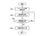
図1は本発明の第1の実施形態に係るパワーモジュール用基板の概略構成を示す断面図、図2は本発明の第1の実施形態のパワーモジュール用基板に用いるセラミックス基板を電子プローブマイクロアナライザにより定量分析した結果を示す表、図3は本発明の第1の実施形態のパワーモジュール用基板の製造方法を説明するフローチャート、図4は本発明の第1の実施形態に係るパワーモジュール用基板を備えるパワーモジュールの概略構成を示す断面図である。 FIG. 1 is a cross-sectional view showing a schematic configuration of a power module substrate according to the first embodiment of the present invention, and FIG. 2 shows an electronic probe microanalyzer used as the ceramic substrate for the power module substrate of the first embodiment of the present invention. FIG. 3 is a flowchart illustrating a method for manufacturing a power module substrate according to the first embodiment of the present invention, and FIG. 4 is a power module substrate according to the first embodiment of the present invention. It is sectional drawing which shows schematic structure of a power module provided with.
図1に示すように、本実施形態におけるパワーモジュール用基板1は、セラミックス基板11と、セラミックス基板11の下面に配置された金属層(金属部材)12と、セラミックス基板11の上面に配置された複数の回路層(金属部材)13とを備えている。すなわち、セラミックス基板11を上下面から挟むようにして、表面に金属部材が接合された構成とされている。 As shown in FIG. 1, the
セラミックス基板11は、Si(珪素)を含有してなるSi3N4(窒化珪素)からなり、板状に形成されている。
また、セラミックス基板11の上下面それぞれにおける酸化シリコン及びシリコンの複合酸化物の濃度は、EPMA(電子プローブマイクロアナライザ)を用いた表面測定において2.7Atom%以下となっている。The
The concentration of silicon oxide and silicon composite oxide on each of the upper and lower surfaces of the
ここで、EPMAを用いた表面測定方法について、図2を参照しながら説明する。
なお、図2に示す定量分析結果は、表面測定方法を説明するために使用する一例である。
本実施形態では、JEOL社製のJXA−8600を用いており、動作圧力を1.3×10⁻³Pa、加速電圧を15.0kV、プローブに供給する電流を5.0×10⁻⁸Aとしている。また、セラミックス基板11の表面には、膜厚が100nm未満であるAu膜が蒸着により形成されている。Here, a surface measurement method using EPMA will be described with reference to FIG.
The quantitative analysis result shown in FIG. 2 is an example used to explain the surface measurement method.
In this embodiment, JXA-8600 manufactured by JEOL is used, the operating pressure is 1.3 × 10⁻³ Pa, the acceleration voltage is 15.0 kV, and the current supplied to the probe is 5.0 × 10⁻⁸ A. It is said. Further, an Au film having a film thickness of less than 100 nm is formed on the surface of the
まず、上記条件でセラミックス基板11の表面を定量分析する(図2(a)に示すA)。そして、定量分析により検出された元素のうちC(炭素)とAu(金)の検出量を0とする(図2(a)に示すB)。さらに、CとAuとを除く他の元素の検出量の和が100Atom%となるように換算する(図2(a)に示すC)。
次に、Si(シリコン)以外の金属元素が最も一般的な酸化物(例えば、Al2O3(アルミナ)、Y2O3(酸化イットリウム)、MgO(酸化マグネシウム)、Er2O3(酸化エルビウム)など)として存在していると仮定し、Si以外の金属元素に結合しているO(酸素)の原子量を算出する(図2(b))。
続いて、換算したOの原子量とSi以外の金属元素に結合しているOの原子量との差を算出する。そして、算出したOの全量がSiと結合してSiO2を構成しているものとし、算出したOの原子量に1.5を乗じて得た値をセラミックス基板11の表面におけるSiO2濃度とする。例えば、図2に示す定量分析結果例では、SiO2濃度が0.253Atom%となる。
なお、EPMAを用いた表面測定は、セラミックス基板11の上面における任意の5箇所において測定している。ここで、表面測定は、5点測定に限らず、10点測定や他の複数個所であってもよい。First, the surface of the
Next, metal elements other than Si (silicon) are the most common oxides (for example, Al2 O3 (alumina), Y2 O3 (yttrium oxide), MgO (magnesium oxide), Er2 O3 (oxidation). 2), the atomic weight of O (oxygen) bonded to a metal element other than Si is calculated (FIG. 2B).
Subsequently, the difference between the converted atomic weight of O and the atomic weight of O bonded to a metal element other than Si is calculated. The calculated total amount of O is combined with Si to constitute SiO2 , and the value obtained by multiplying the calculated atomic amount of O by 1.5 is the SiO2 concentration on the surface of the
In addition, the surface measurement using EPMA is measured in arbitrary five places on the upper surface of the
金属層12は、例えばAl(アルミニウム)などの高熱伝導率を有する金属により形成されており、ロウ材層14によりセラミックス基板11に接合されている。
回路層13は、金属層12と同様に例えばAlなどの高熱伝導率を有する金属により形成されており、間隔を適宜あけて配置されることで回路を構成する。そして、回路層13は、ロウ材層15によりセラミックス基板11に接合されている。
また、回路層13の上面には、電子部品16がハンダ層17により固着されている。電子部品16としては、例えばIGBT(Insulated Gate Bipolar Transistor)などのパワーデバイスが挙げられる。The
The
An
次に、以上のような構成のパワーモジュール用基板1の製造方法について、図3を参照しながら説明する。
まず、セラミックス基板11の基材であり、該セラミックス基板11と略同形状のSi3N4からなるセラミックス母材を用意し、このセラミックス母材を、S10に示すように焼成(焼結)する(焼結工程)。焼結後のセラミックス母材の表面には、焼結時に生じた、Siからなる酸化シリコン及びシリコンの複合酸化物が存在している。Next, a method for manufacturing the
First, a ceramic base material made of Si3 N4 which is a base material of the
次いで、表面処理工程として、S20に示すように、このセラミックス母材の表面にフッ化物イオンを含むガスを用いてプラズマエッチング又は反応性イオンエッチングによりドライエッチングを施す。前記ガスは、主ガス、副ガス及びキャリアガスを混合して構成されており、具体的には、主ガスはフッ化炭素(CnF2n+2、CnF2n等)、フッ化窒素(NF3等)の少なくとも一つからなり、副ガスはH2、SF6(六フッ化硫黄)又は希ガスからなり、キャリアガスはAr+、Ne+、He+(イオンビームとして)からなる。Next, as a surface treatment step, as shown in S20, dry etching is performed on the surface of the ceramic base material by plasma etching or reactive ion etching using a gas containing fluoride ions. The gas is configured by mixing a main gas, a sub gas, and a carrier gas. Specifically, the main gas is carbon fluoride (Cn F2n + 2 , Cn F2n, etc.), nitrogen fluoride (NF)3 ), the secondary gas is H2 , SF6 (sulfur hexafluoride) or a rare gas, and the carrier gas is Ar+ , Ne+ , He+ (as an ion beam).
なお、副ガスとしてH2を用いた場合には、SiO2のエッチングレート比を確実に高めることができ、SF6を用いた場合には、SF5+がキャリアガスとなる。又、副ガスとして希ガスを用いた場合には、ガスのフッ素濃度を下げることでSiO2のエッチングレート比を高めることができる。Note that when H2 is used as the sub-gas, the etching rate ratio of SiO2 can be reliably increased, and when SF6 is used, SF5+ becomes the carrier gas. Further, when a rare gas is used as the auxiliary gas, the SiO2 etching rate ratio can be increased by lowering the fluorine concentration of the gas.
表面処理工程においては、セラミックス母材の表面のSiO2は前記ガスと反応して、主にSiF4とNOx又はCOxとなり、ガス化されセラミックス母材の表面から除去される。このように、セラミックス母材の表面の酸化シリコン及びシリコンの複合酸化物は精度よく除去される。In the surface treatment process, the SiO2 on the surface of the ceramic base material reacts with the gas to mainly become SiF4 and NOx or COx, which is gasified and removed from the surface of the ceramic base material. Thus, silicon oxide and silicon composite oxide on the surface of the ceramic base material are removed with high accuracy.
なお、前記ガスに水素が含まれる場合には、セラミックス母材の表面にNH4Fや(NH4)2SiF6が形成されるが、これらNH4Fや(NH4)2SiF6は、後工程において除去することが好ましい。
また図示しないが、表面処理工程後は、セラミックス母材を蒸留水洗浄工程において洗浄し、乾燥工程においてエアブロー乾燥し、さらにエタノールを用いた超音波洗浄工程において洗浄することが好ましい。When hydrogen is contained in the gas, NH4 F and (NH4 )2 SiF6 are formed on the surface of the ceramic base material. These NH4 F and (NH4 )2 SiF6 are It is preferable to remove in a subsequent step.
Although not shown, after the surface treatment process, it is preferable to clean the ceramic base material in a distilled water cleaning process, air blow dry in a drying process, and further clean in an ultrasonic cleaning process using ethanol.
次いで、表面測定工程として、S30に示すように、表面処理工程後のセラミックス母材の表面における酸化シリコン及びシリコンの複合酸化物の濃度をEPMAにより表面測定し、2.7Atom%以下であるか確認する。なお、EPMAによる表面測定方法は、上述と同様である。また、EPMAによる表面測定は、セラミックス母材の表面における任意の5箇所において測定している。
表面測定工程の結果が2.7Atom%以下であれば、セラミックス基板11の製造が終了し、次工程へと移行する。
表面測定工程の結果が2.7Atom%を超える場合には、セラミックス母材に再度S20の表面処理工程が施される。Next, as a surface measurement step, as shown in S30, the concentration of silicon oxide and silicon composite oxide on the surface of the ceramic base material after the surface treatment step is measured by EPMA to confirm that it is 2.7 Atom% or less. To do. The surface measurement method using EPMA is the same as described above. Moreover, the surface measurement by EPMA is measured in arbitrary five places on the surface of the ceramic base material.
If the result of the surface measurement step is 2.7 Atom% or less, the production of the
When the result of the surface measurement process exceeds 2.7 Atom%, the surface treatment process of S20 is performed again on the ceramic base material.
次に、パワーモジュール用基板1の製造のための金属部材接合工程として、S40に示すように、セラミックス基板11の上下両面に、金属層12及び回路層13それぞれの金属部材をロウ付けにより一体に接合する。
以上のようにして、パワーモジュール用基板1を製造する。Next, as a metal member joining step for manufacturing the
The
以上説明したように、パワーモジュール用基板1のセラミックス基板11の上下両面においては、S20の表面処理工程で酸化シリコン及びシリコンの複合酸化物が精度よく除去されているため、接合時においてこれら酸化シリコン及びシリコンの複合酸化物に起因するSiO(一酸化珪素)ガスの発生が抑制されている。 As described above, on both the upper and lower surfaces of the
すなわち、表面処理工程において、セラミックス母材の表面の酸化シリコン及びシリコンの複合酸化物がフッ化物イオンと反応し、揮発性の高いSiF4ガス等となり表面から除去されるため、該表面における酸化シリコン及びシリコンの複合酸化物の濃度が前記表面測定で2.7Atom%以下にまで確実に低減されるようになっている。従って、このようにして製造されたセラミックス基板11と金属部材とを接合した際に、酸化シリコン及びシリコンの複合酸化物に起因するSiOガスの発生が抑制されることから、回路層13及びセラミックス基板11との接合面積と金属層12及びセラミックス基板11との接合面積とのそれぞれが充分に確保されるとともに、熱サイクル時におけるセラミックス基板11と金属部材との剥離が防止されて、接合信頼性が高められている。That is, in the surface treatment step, the silicon oxide and silicon composite oxide on the surface of the ceramic base material react with fluoride ions to be removed from the surface as a highly volatile SiF4 gas, etc. In addition, the concentration of the complex oxide of silicon is reliably reduced to 2.7 Atom% or less in the surface measurement. Therefore, when the
また、ドライエッチングのガスに含まれるフッ化物イオンは、前述した反応により揮発性の高いSiF4ガスとなることから、セラミックス母材の表面にフッ化物として残留することがない。また、ドライエッチングは、例えばセラミックス母材をウェットエッチングする場合と対比して反応の回り込みが少ないため、必要以上に焼結助剤に反応してフッ化物が残留してしまうことが抑制される。In addition, fluoride ions contained in the dry etching gas become highly volatile SiF4 gas due to the above-described reaction, and therefore do not remain as fluoride on the surface of the ceramic base material. Further, since dry etching has less wraparound of the reaction as compared with, for example, wet etching of a ceramic base material, it is possible to suppress the fluoride from remaining in response to the sintering aid more than necessary.
また、ドライエッチングでは、セラミックス母材において表面のSiO2をエッチングして除去し、Si3N4に達するとエッチング反応が抑制されるため、効率よくSiO2のみを除去することができる。
従って、セラミックス基板11と金属部材とを接合した際に、フッ化物に起因して接合不良が生じるようなことが防止され、セラミックス基板11と金属部材との接合信頼性が確実に高められている。In dry etching, SiO2 on the surface of the ceramic base material is removed by etching, and when Si3 N4 is reached, the etching reaction is suppressed, so that only SiO2 can be efficiently removed.
Therefore, when the
また、接合時において、Al2O3と共にSiOガスが発生することを抑制するので、セラミックス基板11と金属部材とを充分な強度で接合することができる。すなわち、セラミックス基板11と金属部材とを接合する際、セラミックス基板11の表面に酸化シリコン又はシリコンの複合酸化物が存在すると、金属部材におけるセラミックス基板11との界面及びその近傍にアルミニウムの酸化物であるアルミナが形成されると共に一酸化珪素ガスが発生するのだが、セラミックス基板11の表面の酸化シリコン及びシリコンの複合酸化物が表面処理により良好に除去されているので、接合時における一酸化珪素ガスの発生が抑制されている。Further, at the time of joining, since SiO gas can be inhibited to occur with Al2 O3, it is possible to bond the
また、ドライエッチング後のセラミックス基材11の表面にはフッ化物が残留しないことから、前記表面にAlF3(フッ化アルミニウム)が発生することが防止され、AlF3に起因してセラミックス基板11と金属部材との接合強度が低減させられることがない。従って、セラミックス基板11と金属部材との接合強度が充分に確保される。Further, since no residual fluoride on the surface of the
このような構成のパワーモジュール用基板1においては、セラミックス基板11と金属部材との接合面積及び接合強度が充分に確保されているため、温度サイクル試験における例えば1000サイクル程度までの間に、回路層13や金属層12がセラミックス基板11から剥離することが確実に抑制される。 In the
尚、図3において説明したS30の表面測定工程は、その測定結果が安定して2.7Atom%以下に得られる場合には、省略してもよい。
また、S20の表面処理工程は、S40の金属部材接合工程の接合直前に行われることがより好ましい。
また、S30の表面測定工程の結果が2.7Atom%を超えた場合に、前述のようにセラミックス母材に再度S20の表面処理工程を施さずに、廃棄することとしてもよく、種々の要望・用途に対応して選択可能である。Note that the surface measurement step of S30 described in FIG. 3 may be omitted when the measurement result is stably obtained at 2.7 Atom% or less.
Moreover, it is more preferable that the surface treatment process of S20 is performed immediately before joining of the metal member joining process of S40.
In addition, when the result of the surface measurement step of S30 exceeds 2.7 Atom%, the ceramic base material may be discarded without performing the surface treatment step of S20 again as described above. It can be selected according to the application.
このようにして製造されたパワーモジュール用基板1は、例えば図4に示すようなパワーモジュール30に用いられる。このパワーモジュール30は、上述のパワーモジュール用基板1と、電子部品16と、冷却器31と、放熱板32とを備えている。
冷却器31は、水冷式のヒートシンクであって、内部に冷媒である冷却水が流通する流路が形成されている。
放熱板32は、平面視でほぼ矩形状の平板形状を有しており、例えばAlやCu(銅)、AlSiC(アルミシリコンカーバイド)、Cu−Mo(モリブデン)などで形成されている。The
The cooler 31 is a water-cooled heat sink, and a flow path through which cooling water as a coolant flows is formed.
The
そして、放熱板32は、熱伝導グリースなどを介して冷却器31に対してネジ33により固定されている。また、放熱板32とパワーモジュール用基板1の金属層12とは、ハンダ層34により接合されている。なお、放熱板32と金属層12とは、ロウ付けにより接合されてもよい。このとき、パワーモジュール用基板1の製造時において、金属層12、セラミックス基板11及び回路層13の積層体に放熱板32をさらに積層した状態で各部材を一括してロウ付けしてもよい。また、パワーモジュール30は、放熱板32を設けずに冷却器31の上面にパワーモジュール用基板1を設ける構成としてもよい。 And the
次に、本発明の第2の実施形態のパワーモジュール用基板の製造方法について、図5を参照しながら説明する。
図5は本発明の第2の実施形態に係るパワーモジュール用基板の製造方法を説明する工程図である。
尚、前述の第1の実施形態と同一部材には同一の符号を付し、その説明を省略する。Next, the manufacturing method of the board | substrate for power modules of the 2nd Embodiment of this invention is demonstrated, referring FIG.
FIG. 5 is a process diagram illustrating a method for manufacturing a power module substrate according to the second embodiment of the present invention.
In addition, the same code | symbol is attached | subjected to the same member as above-mentioned 1st Embodiment, and the description is abbreviate | omitted.
まず、Si3N4からなり、焼成(焼結)された後のセラミックス母材20を用意する。セラミックス母材20の表面には、焼結時に生じたSiからなる酸化シリコン及びシリコンの複合酸化物が存在している。このセラミックス母材20の一面に、図5(a)に示すように、複数のスクライブライン21を形成する。First, a
ここでは、セラミックス母材20の一面にレーザ光(エネルギー光)Lを照射することで、直線状のスクライブライン21を形成する。このとき、レーザ光Lの照射によりセラミックス母材20から飛散するヒューム22が、スクライブライン21の形成領域及びその近傍に付着する。このヒューム22も、セラミックス母材20がSi3N4からなるため、酸化シリコン及びシリコンの複合酸化物で形成されている。Here, a
次いで、第1の表面処理として、セラミックス母材20の上下両面にZrO2(二酸化ジルコニウム)粉末を噴き付けるブラスト処理を施す(図5(b))。これにより、セラミックス母材20の上下両面の平坦化を行うと共に、セラミックス母材20の一面に付着しているヒューム22を除去する。Next, as a first surface treatment, a blast treatment is performed in which ZrO2 (zirconium dioxide) powder is sprayed onto the upper and lower surfaces of the ceramic base material 20 (FIG. 5B). Thereby, the upper and lower surfaces of the
次いで、第2の表面処理として、図5(c)に示すように、ヒューム22を除去したセラミックス母材20を容器状のドライエッチング装置Pに収容し、このドライエッチング装置Pにフッ化物イオンを含むガスGを流入して、ドライエッチングを施す。ガスGは、前述した主ガス、副ガス及びキャリアガスを混合して構成されている。 Next, as a second surface treatment, as shown in FIG. 5C, the
ガスGは、セラミックス母材20の表面の酸化シリコン及びシリコンの複合酸化物と反応して、主にSiF4とNOx又はCOxとなり、これら酸化シリコン及びシリコンの複合酸化物はセラミックス母材の表面から除去されるとともに、排気ガスEとしてドライエッチング装置Pから排出される。このように、ドライエッチングによって、セラミックス母材20の表面の酸化シリコン及びシリコンの複合酸化物が精度よく除去されるようになっている。The gas G reacts mainly with the silicon oxide and silicon composite oxide on the surface of the
尚、ガスGに水素が含まれる場合には、セラミックス母材20の表面にNH4Fや(NH4)2SiF6が形成されるが、これらNH4Fや(NH4)2SiF6は、後工程において除去することが好ましい。
また図示しないが、ドライエッチング後は、このセラミックス母材20を蒸留水洗浄工程において洗浄し、乾燥工程においてエアブロー乾燥し、さらにエタノールを用いた超音波洗浄工程において洗浄した後、乾燥雰囲気において保管することが好ましい。When the gas G contains hydrogen, NH4 F and (NH4 )2 SiF6 are formed on the surface of the
Although not shown, after dry etching, the
ドライエッチング後のセラミックス母材20の表面における酸化シリコン及びシリコンの複合酸化物の濃度は、EPMAによる表面測定において2.7Atom%以下にまで低減されている。なお、EPMAによる表面測定方法は、上述と同様である。また、EPMAによる表面測定は、セラミックス母材20においてスクライブライン21で区画される複数の領域それぞれで任意の5箇所において測定している。 The concentration of silicon oxide and silicon composite oxide on the surface of the
次に、セラミックス母材20をスクライブライン21に沿って分割する(図5(d))。このようにして、セラミックス基板41が製造される。そして、製造したセラミックス基板41の上下両面に、金属層12及び回路層13それぞれをロウ付けにより接合する(図5(e))。
以上のようにして、パワーモジュール用基板51を製造する。Next, the
The
以上説明したように、本実施形態のセラミックス基板41を備えたパワーモジュール用基板51においても、前述した第1の実施形態と同様の作用効果を奏する。
このような構成のパワーモジュール用基板51においては、セラミックス基板41と金属部材との接合面積及び接合強度が充分に確保されているため、温度サイクル試験における例えば1000サイクル程度までの間に、回路層13や金属層12がセラミックス基板41から剥離することが確実に抑制される。As described above, the
In the
尚、本発明は上記実施形態に限定されるものではなく、本発明の趣旨を逸脱しない範囲において種々の変更を加えることができる。
例えば、第2の実施形態のセラミックス基板の製造方法では、焼結後のセラミックス母材20にスクライブライン21を設け、スクライブライン21の形成時に生じるヒューム22をブラスト処理で除去することとして説明したが、これに限定されるものではない。すなわち、スクライブライン21の代わりにカッター等を用いてセラミックス母材20を切断して複数のセラミックス基板41とし、前述のブラスト処理を省略しても構わない。In addition, this invention is not limited to the said embodiment, A various change can be added in the range which does not deviate from the meaning of this invention.
For example, in the method for manufacturing a ceramic substrate according to the second embodiment, the
また第1、第2の実施形態では、セラミックス基板11,41の上下両面における酸化シリコン及びシリコンの複合酸化物の濃度を2.7Atom%以下とすることとして説明したが、これに限らず、少なくとも金属部材が接合される表面部分における酸化シリコン及びシリコンの複合酸化物の濃度が2.7Atom%以下であればよい。すなわち、セラミックス基板11,41において、接合する金属部材の形状に対応した表面部分のみ、酸化シリコン及びシリコンの複合酸化物の濃度を2.7Atom%以下とすることとしても構わない。 In the first and second embodiments, the concentration of the silicon oxide and the silicon composite oxide on the upper and lower surfaces of the
また第1、第2の実施形態では、セラミックス基板11,41の一面を上面として回路層13を接合しているが、一面を下面として金属層12を接合する構成としてもよい。
また、セラミックス基板11,41と回路層13または金属層12とは、ロウ付け接合されていることとして説明したが、それ以外の方法により接合されていても構わない。In the first and second embodiments, the
In addition, the
また第2の実施形態では、セラミックス母材20を分割してセラミックス基板41を形成した後に金属層12及び回路層13それぞれを接合しているが、スクライブライン21が形成されたセラミックス母材20に金属層12及び回路層13の少なくとも一方を接合した後に該セラミックス母材20を分割してセラミックス基板41を形成してもよい。
また、スクライブライン21は、レーザ光Lを照射することで形成されているが、それ以外の他のエネルギー光の照射により形成されてもよい。In the second embodiment, the
Moreover, although the
また、スクライブライン21を形成した場合の第1の表面処理としては、粉末の噴き付けによるブラスト処理のほか、ホーニング処理などそれ以外の処理を用いても構わない。
また、金属層12及び回路層13それぞれは、アルミニウムで形成されていることとして説明したが、それ以外の金属材料で形成されていてもよい。Further, as the first surface treatment when the
Further, the
また、パワーモジュール用基板1,51は、セラミックス基板11,41の下面に金属層12を接合しているが、金属層12を設けずにセラミックス基板11,41の下面に放熱板32や冷却器31を直接接合する構成としても構わない。
また、冷却器31は、本実施形態の水冷式に限らずに、空冷式や他の液冷式であっても構わない。Further, the
The cooler 31 is not limited to the water-cooled type of the present embodiment, and may be an air-cooled type or other liquid-cooled type.
また、セラミックス基板11,41は、Siを含有するSi3N4からなるとして説明したが、これに限定されるものではなく、Siを含有するそれ以外の材料であっても構わない。Further, the
また第1、第2の実施形態では、ドライエッチングに用いるガスは、主ガスがフッ化炭素(CnF2n+2、CnF2n等)、フッ化窒素(NF3等)の少なくとも一つからなり、副ガスがH2、SF6(六フッ化硫黄)又は希ガスからなることとして説明したが、これらに限定されるものではない。The first, in the second embodiment, the gas used for dry etching, the main gas is carbon fluoride(C n F 2n + 2, C n F 2n , etc.), from at least one of nitrogen fluoride (NF3, etc.) It has been described that the auxiliary gas is made of H2 , SF6 (sulfur hexafluoride) or a rare gas, but is not limited thereto.
1,51 パワーモジュール用基板
11,41 セラミックス基板
12 金属層(金属部材)
13 回路層(金属部材)
14,15 ロウ材層
20 セラミックス母材
G ガス
P ドライエッチング装置
S10 焼結工程
S20 表面処理工程(ドライエッチング)
S30 表面測定工程
S40 金属部材接合工程1,51
13 Circuit layer (metal member)
14, 15
S30 Surface measurement process S40 Metal member joining process
Claims (5)
Translated fromJapaneseSiを含有するセラミックス母材を焼結する工程と、
前記セラミックス母材の表面にフッ化物イオンを含むガスを用いてドライエッチングを施す表面処理工程と、を備え、
前記表面処理工程において、前記セラミックス母材の表面のうち少なくとも前記金属部材が接合される表面部分の酸化シリコン及びシリコンの複合酸化物の濃度を電子プローブマイクロアナライザを用いた表面測定で2.7Atom%以下とすることを特徴とするパワーモジュール用基板のセラミックス基板の製造方法。A method for manufacturing a ceramic substrate of a power module substrate, wherein a metal member is bonded to a ceramic substrate,
Sintering a ceramic matrix containing Si;
A surface treatment step of performing dry etching on the surface of the ceramic base material using a gas containing fluoride ions,
In the surface treatment step, the concentration of silicon oxide and silicon composite oxide inat least the surface portion of the ceramic base material towhich the metal member is bonded is 2.7 Atom% by surface measurement using an electron probe microanalyzer. following a toTurkey the method of manufacturing the ceramic substrateof the power module substrate according to claim.
前記ガスは、少なくともフッ化炭素及びフッ化窒素のうちいずれかを含むことを特徴とするパワーモジュール用基板のセラミックス基板の製造方法。A method for producinga ceramic substratefor apower module substrate according to claim 1,
The method for producinga ceramic substrate of apower module substrate, wherein the gas contains at least one of carbon fluoride and nitrogen fluoride.
前記金属部材として、アルミニウムを用いることを特徴とするパワーモジュール用基板の製造方法。It is a manufacturing method of the board for power modules according to claim 3,
The manufacturing method of the board | substrate for power modules characterized by using aluminum as said metal member.
前記セラミックス基板と前記金属部材との接合が、ロウ付けで行われることを特徴とするパワーモジュール用基板の製造方法。A method for producing a power module substrate according to claim 3 or 4,
A method of manufacturing a power module substrate, wherein the ceramic substrate and the metal member are joined by brazing.
Priority Applications (6)
| Application Number | Priority Date | Filing Date | Title |
|---|---|---|---|
| JP2008271036AJP5309885B2 (en) | 2008-10-21 | 2008-10-21 | Method for manufacturing ceramic substrate for power module substrate and method for manufacturing power module substrate |
| US12/734,428US20100258233A1 (en) | 2007-11-06 | 2008-11-06 | Ceramic substrate, method of manufacturing ceramic substrate, and method of manufacturing power module substrate |
| PCT/JP2008/070219WO2009060902A1 (en) | 2007-11-06 | 2008-11-06 | Ceramic substrate, method for producing ceramic substrate, and method for producing substrate for power module |
| EP08846400.3AEP2217043B1 (en) | 2007-11-06 | 2008-11-06 | Method for producing a substrate for power module |
| CN2008801146408ACN101849445B (en) | 2007-11-06 | 2008-11-06 | Ceramic substrate, method for producing ceramic substrate, and method for producing substrate for power module |
| US13/867,439US9079264B2 (en) | 2007-11-06 | 2013-04-22 | Ceramic substrate, method of manufacturing ceramic substrate, and method of manufacturing power module substrate |
Applications Claiming Priority (1)
| Application Number | Priority Date | Filing Date | Title |
|---|---|---|---|
| JP2008271036AJP5309885B2 (en) | 2008-10-21 | 2008-10-21 | Method for manufacturing ceramic substrate for power module substrate and method for manufacturing power module substrate |
Publications (2)
| Publication Number | Publication Date |
|---|---|
| JP2010103168A JP2010103168A (en) | 2010-05-06 |
| JP5309885B2true JP5309885B2 (en) | 2013-10-09 |
Family
ID=42293589
Family Applications (1)
| Application Number | Title | Priority Date | Filing Date |
|---|---|---|---|
| JP2008271036AActiveJP5309885B2 (en) | 2007-11-06 | 2008-10-21 | Method for manufacturing ceramic substrate for power module substrate and method for manufacturing power module substrate |
Country Status (1)
| Country | Link |
|---|---|
| JP (1) | JP5309885B2 (en) |
Cited By (1)
| Publication number | Priority date | Publication date | Assignee | Title |
|---|---|---|---|---|
| US9085121B2 (en) | 1999-05-13 | 2015-07-21 | 3M Innovative Properties Company | Adhesive-backed articles |
Families Citing this family (1)
| Publication number | Priority date | Publication date | Assignee | Title |
|---|---|---|---|---|
| US10426043B2 (en)* | 2016-08-19 | 2019-09-24 | Honeywell Federal Manufacturing & Technologies, Llc | Method of thin film adhesion pretreatment |
Family Cites Families (8)
| Publication number | Priority date | Publication date | Assignee | Title |
|---|---|---|---|---|
| JPH02107579A (en)* | 1988-10-17 | 1990-04-19 | Yoshino Hard:Kk | Joining method for ceramic |
| JP2519578B2 (en)* | 1990-06-11 | 1996-07-31 | 東洋鋼鈑株式会社 | Method of joining metal member and ceramics or cermet member |
| JPH0729866B2 (en)* | 1991-03-22 | 1995-04-05 | 日本碍子株式会社 | Surface modification method of silicon nitride sintered body and joining method of sintered body |
| JPH10130059A (en)* | 1996-10-24 | 1998-05-19 | Toshiba Ceramics Co Ltd | Production of high purity silicon nitride body |
| JP2004231513A (en)* | 2000-10-26 | 2004-08-19 | Hitachi Metals Ltd | Circuit board excellent in high strength/high heat conductivity |
| JP5075308B2 (en)* | 2001-07-11 | 2012-11-21 | 株式会社東芝 | Manufacturing method of ceramic circuit board |
| JP2002128567A (en)* | 2001-09-14 | 2002-05-09 | Ngk Spark Plug Co Ltd | Silicon nitride sintered compact and its manufacturing method |
| JP4715414B2 (en)* | 2005-09-22 | 2011-07-06 | 日立金属株式会社 | Silicon nitride wiring board and manufacturing method thereof |
- 2008
- 2008-10-21JPJP2008271036Apatent/JP5309885B2/enactiveActive
Cited By (1)
| Publication number | Priority date | Publication date | Assignee | Title |
|---|---|---|---|---|
| US9085121B2 (en) | 1999-05-13 | 2015-07-21 | 3M Innovative Properties Company | Adhesive-backed articles |
Also Published As
| Publication number | Publication date |
|---|---|
| JP2010103168A (en) | 2010-05-06 |
Similar Documents
| Publication | Publication Date | Title |
|---|---|---|
| US9079264B2 (en) | Ceramic substrate, method of manufacturing ceramic substrate, and method of manufacturing power module substrate | |
| CN101529588B (en) | Power module substrate, method for manufacturing power module substrate, and power module | |
| JP6729224B2 (en) | Ceramic/aluminum bonded body, insulated circuit board, power module, LED module, thermoelectric module | |
| TW201423922A (en) | Substrate with heat sink power module, heat sink power module, and manufacturing method of substrate for heat sink power module | |
| KR20170044105A (en) | Joined body, substrate for power module provided with heat sink, heat sink, method for manufacturing joined body, method for manufacturing substrate for power module provided with heat sink, and method for manufacturing heat sink | |
| JP6656657B2 (en) | Ceramic / aluminum joint, power module substrate, and power module | |
| TW201517225A (en) | Power module | |
| JP4360847B2 (en) | Ceramic circuit board, heat dissipation module, and semiconductor device | |
| JP5309885B2 (en) | Method for manufacturing ceramic substrate for power module substrate and method for manufacturing power module substrate | |
| JP5422964B2 (en) | Method for manufacturing ceramic substrate and method for manufacturing substrate for power module | |
| JP5176627B2 (en) | Ceramic substrate for power module substrate, method for manufacturing ceramic substrate for power module substrate, and method for manufacturing power module substrate | |
| JP3779074B2 (en) | Ceramic circuit board and power module using it | |
| JP6750422B2 (en) | Method for manufacturing insulated circuit board, insulated circuit board, power module, LED module, and thermoelectric module | |
| JP6031784B2 (en) | Power module substrate and manufacturing method thereof | |
| JP7424043B2 (en) | Copper/ceramic bonded body, insulated circuit board, method for manufacturing copper/ceramic bonded body, method for manufacturing insulated circuit board | |
| CN104813466B (en) | Manufacturing method of substrate for power module | |
| JP7587364B2 (en) | Insulating substrate and method for manufacturing the same | |
| JP5039070B2 (en) | Semiconductor device | |
| HK1147159A (en) | Ceramic substrate, method for producing ceramic substrate, and method for producing substrate for power module | |
| JP2023044872A (en) | Copper/ceramic joint body and insulated circuit board | |
| JP2023020265A (en) | Copper/Ceramic Bonded Body and Insulated Circuit Board | |
| JP7243165B2 (en) | Method for manufacturing bonded body, method for manufacturing insulated circuit board, ceramic substrate, bonded body, and insulated circuit board | |
| JP2000049425A (en) | Ceramic circuit board, method of manufacturing the same, and power module using the same | |
| JP2011077087A (en) | Substrate for power module and method of manufacturing the same | |
| WO2023120654A1 (en) | Ceramic scribe circuit substrate, ceramic circuit substrate, method for manufacturing ceramic scribe circuit substrate, method for manufacturing ceramic circuit substrate, and method for manufacturing semiconductor device |
Legal Events
| Date | Code | Title | Description |
|---|---|---|---|
| A621 | Written request for application examination | Free format text:JAPANESE INTERMEDIATE CODE: A621 Effective date:20110928 | |
| A131 | Notification of reasons for refusal | Free format text:JAPANESE INTERMEDIATE CODE: A131 Effective date:20130319 | |
| A521 | Request for written amendment filed | Free format text:JAPANESE INTERMEDIATE CODE: A523 Effective date:20130515 | |
| TRDD | Decision of grant or rejection written | ||
| A521 | Request for written amendment filed | Free format text:JAPANESE INTERMEDIATE CODE: A821 Effective date:20130515 | |
| A01 | Written decision to grant a patent or to grant a registration (utility model) | Free format text:JAPANESE INTERMEDIATE CODE: A01 Effective date:20130604 | |
| A61 | First payment of annual fees (during grant procedure) | Free format text:JAPANESE INTERMEDIATE CODE: A61 Effective date:20130617 | |
| R150 | Certificate of patent or registration of utility model | Free format text:JAPANESE INTERMEDIATE CODE: R150 Ref document number:5309885 Country of ref document:JP Free format text:JAPANESE INTERMEDIATE CODE: R150 | |
| R250 | Receipt of annual fees | Free format text:JAPANESE INTERMEDIATE CODE: R250 | |
| R250 | Receipt of annual fees | Free format text:JAPANESE INTERMEDIATE CODE: R250 |