JP5306989B2 - Method for simultaneously patterning a substrate having a plurality of fields and alignment marks - Google Patents
Method for simultaneously patterning a substrate having a plurality of fields and alignment marksDownload PDFInfo
- Publication number
- JP5306989B2 JP5306989B2JP2009504287AJP2009504287AJP5306989B2JP 5306989 B2JP5306989 B2JP 5306989B2JP 2009504287 AJP2009504287 AJP 2009504287AJP 2009504287 AJP2009504287 AJP 2009504287AJP 5306989 B2JP5306989 B2JP 5306989B2
- Authority
- JP
- Japan
- Prior art keywords
- substrate
- template
- alignment
- field
- pattern
- Prior art date
- Legal status (The legal status is an assumption and is not a legal conclusion. Google has not performed a legal analysis and makes no representation as to the accuracy of the status listed.)
- Expired - Fee Related
Links
- 239000000758substrateSubstances0.000titleclaimsabstractdescription169
- 238000000034methodMethods0.000titleclaimsabstractdescription43
- 238000000059patterningMethods0.000titleclaimsabstractdescription15
- 239000000463materialSubstances0.000claimsabstractdescription16
- 230000015572biosynthetic processEffects0.000claimsdescription25
- VYPSYNLAJGMNEJ-UHFFFAOYSA-NSilicium dioxideChemical compoundO=[Si]=OVYPSYNLAJGMNEJ-UHFFFAOYSA-N0.000claimsdescription4
- 239000005350fused silica glassSubstances0.000claimsdescription3
- 239000011521glassSubstances0.000claimsdescription2
- 230000008878couplingEffects0.000claims2
- 238000010168coupling processMethods0.000claims2
- 238000005859coupling reactionMethods0.000claims2
- 239000002861polymer materialSubstances0.000description30
- 238000001459lithographyMethods0.000description9
- 238000009826distributionMethods0.000description7
- 239000012530fluidSubstances0.000description7
- 238000000206photolithographyMethods0.000description5
- 238000005229chemical vapour depositionMethods0.000description4
- 238000000609electron-beam lithographyMethods0.000description4
- 238000005240physical vapour depositionMethods0.000description4
- 238000012937correctionMethods0.000description3
- 238000000151depositionMethods0.000description3
- 239000007788liquidSubstances0.000description3
- 238000004519manufacturing processMethods0.000description3
- 238000004891communicationMethods0.000description2
- 230000008021depositionEffects0.000description2
- 238000003618dip coatingMethods0.000description2
- 239000010408filmSubstances0.000description2
- 238000005305interferometryMethods0.000description2
- 230000003287optical effectEffects0.000description2
- 238000012545processingMethods0.000description2
- 230000005855radiationEffects0.000description2
- 238000004528spin coatingMethods0.000description2
- 238000000427thin-film depositionMethods0.000description2
- 238000004458analytical methodMethods0.000description1
- 239000005388borosilicate glassSubstances0.000description1
- -1but not limited toSubstances0.000description1
- 238000011161developmentMethods0.000description1
- KPUWHANPEXNPJT-UHFFFAOYSA-NdisiloxaneChemical class[SiH3]O[SiH3]KPUWHANPEXNPJT-UHFFFAOYSA-N0.000description1
- 238000000203droplet dispensingMethods0.000description1
- 238000005516engineering processMethods0.000description1
- 229920002313fluoropolymerPolymers0.000description1
- 229910052751metalInorganic materials0.000description1
- 239000002184metalSubstances0.000description1
- 150000002739metalsChemical class0.000description1
- 238000012986modificationMethods0.000description1
- 230000004048modificationEffects0.000description1
- 229920000620organic polymerPolymers0.000description1
- 229920000642polymerPolymers0.000description1
- 238000004886process controlMethods0.000description1
- 239000010453quartzSubstances0.000description1
- 229910052594sapphireInorganic materials0.000description1
- 239000010980sapphireSubstances0.000description1
- 239000004065semiconductorSubstances0.000description1
- 238000000926separation methodMethods0.000description1
- 229910052710siliconInorganic materials0.000description1
- 239000010703siliconSubstances0.000description1
- 239000000725suspensionSubstances0.000description1
- 238000013518transcriptionMethods0.000description1
- 230000035897transcriptionEffects0.000description1
Images


Classifications
- B—PERFORMING OPERATIONS; TRANSPORTING
- B29—WORKING OF PLASTICS; WORKING OF SUBSTANCES IN A PLASTIC STATE IN GENERAL
- B29C—SHAPING OR JOINING OF PLASTICS; SHAPING OF MATERIAL IN A PLASTIC STATE, NOT OTHERWISE PROVIDED FOR; AFTER-TREATMENT OF THE SHAPED PRODUCTS, e.g. REPAIRING
- B29C43/00—Compression moulding, i.e. applying external pressure to flow the moulding material; Apparatus therefor
- B29C43/02—Compression moulding, i.e. applying external pressure to flow the moulding material; Apparatus therefor of articles of definite length, i.e. discrete articles
- B29C43/021—Compression moulding, i.e. applying external pressure to flow the moulding material; Apparatus therefor of articles of definite length, i.e. discrete articles characterised by the shape of the surface
- G—PHYSICS
- G03—PHOTOGRAPHY; CINEMATOGRAPHY; ANALOGOUS TECHNIQUES USING WAVES OTHER THAN OPTICAL WAVES; ELECTROGRAPHY; HOLOGRAPHY
- G03F—PHOTOMECHANICAL PRODUCTION OF TEXTURED OR PATTERNED SURFACES, e.g. FOR PRINTING, FOR PROCESSING OF SEMICONDUCTOR DEVICES; MATERIALS THEREFOR; ORIGINALS THEREFOR; APPARATUS SPECIALLY ADAPTED THEREFOR
- G03F7/00—Photomechanical, e.g. photolithographic, production of textured or patterned surfaces, e.g. printing surfaces; Materials therefor, e.g. comprising photoresists; Apparatus specially adapted therefor
- G03F7/0002—Lithographic processes using patterning methods other than those involving the exposure to radiation, e.g. by stamping
- B—PERFORMING OPERATIONS; TRANSPORTING
- B29—WORKING OF PLASTICS; WORKING OF SUBSTANCES IN A PLASTIC STATE IN GENERAL
- B29C—SHAPING OR JOINING OF PLASTICS; SHAPING OF MATERIAL IN A PLASTIC STATE, NOT OTHERWISE PROVIDED FOR; AFTER-TREATMENT OF THE SHAPED PRODUCTS, e.g. REPAIRING
- B29C43/00—Compression moulding, i.e. applying external pressure to flow the moulding material; Apparatus therefor
- B29C43/003—Compression moulding, i.e. applying external pressure to flow the moulding material; Apparatus therefor characterised by the choice of material
- B—PERFORMING OPERATIONS; TRANSPORTING
- B29—WORKING OF PLASTICS; WORKING OF SUBSTANCES IN A PLASTIC STATE IN GENERAL
- B29C—SHAPING OR JOINING OF PLASTICS; SHAPING OF MATERIAL IN A PLASTIC STATE, NOT OTHERWISE PROVIDED FOR; AFTER-TREATMENT OF THE SHAPED PRODUCTS, e.g. REPAIRING
- B29C43/00—Compression moulding, i.e. applying external pressure to flow the moulding material; Apparatus therefor
- B29C43/32—Component parts, details or accessories; Auxiliary operations
- B29C43/58—Measuring, controlling or regulating
- B—PERFORMING OPERATIONS; TRANSPORTING
- B29—WORKING OF PLASTICS; WORKING OF SUBSTANCES IN A PLASTIC STATE IN GENERAL
- B29C—SHAPING OR JOINING OF PLASTICS; SHAPING OF MATERIAL IN A PLASTIC STATE, NOT OTHERWISE PROVIDED FOR; AFTER-TREATMENT OF THE SHAPED PRODUCTS, e.g. REPAIRING
- B29C59/00—Surface shaping of articles, e.g. embossing; Apparatus therefor
- B29C59/02—Surface shaping of articles, e.g. embossing; Apparatus therefor by mechanical means, e.g. pressing
- B29C59/022—Surface shaping of articles, e.g. embossing; Apparatus therefor by mechanical means, e.g. pressing characterised by the disposition or the configuration, e.g. dimensions, of the embossments or the shaping tools therefor
- B—PERFORMING OPERATIONS; TRANSPORTING
- B82—NANOTECHNOLOGY
- B82Y—SPECIFIC USES OR APPLICATIONS OF NANOSTRUCTURES; MEASUREMENT OR ANALYSIS OF NANOSTRUCTURES; MANUFACTURE OR TREATMENT OF NANOSTRUCTURES
- B82Y10/00—Nanotechnology for information processing, storage or transmission, e.g. quantum computing or single electron logic
- B—PERFORMING OPERATIONS; TRANSPORTING
- B82—NANOTECHNOLOGY
- B82Y—SPECIFIC USES OR APPLICATIONS OF NANOSTRUCTURES; MEASUREMENT OR ANALYSIS OF NANOSTRUCTURES; MANUFACTURE OR TREATMENT OF NANOSTRUCTURES
- B82Y40/00—Manufacture or treatment of nanostructures
- G—PHYSICS
- G03—PHOTOGRAPHY; CINEMATOGRAPHY; ANALOGOUS TECHNIQUES USING WAVES OTHER THAN OPTICAL WAVES; ELECTROGRAPHY; HOLOGRAPHY
- G03F—PHOTOMECHANICAL PRODUCTION OF TEXTURED OR PATTERNED SURFACES, e.g. FOR PRINTING, FOR PROCESSING OF SEMICONDUCTOR DEVICES; MATERIALS THEREFOR; ORIGINALS THEREFOR; APPARATUS SPECIALLY ADAPTED THEREFOR
- G03F9/00—Registration or positioning of originals, masks, frames, photographic sheets or textured or patterned surfaces, e.g. automatically
- G03F9/70—Registration or positioning of originals, masks, frames, photographic sheets or textured or patterned surfaces, e.g. automatically for microlithography
- G03F9/7003—Alignment type or strategy, e.g. leveling, global alignment
- G03F9/7023—Aligning or positioning in direction perpendicular to substrate surface
- G03F9/703—Gap setting, e.g. in proximity printer
- G—PHYSICS
- G03—PHOTOGRAPHY; CINEMATOGRAPHY; ANALOGOUS TECHNIQUES USING WAVES OTHER THAN OPTICAL WAVES; ELECTROGRAPHY; HOLOGRAPHY
- G03F—PHOTOMECHANICAL PRODUCTION OF TEXTURED OR PATTERNED SURFACES, e.g. FOR PRINTING, FOR PROCESSING OF SEMICONDUCTOR DEVICES; MATERIALS THEREFOR; ORIGINALS THEREFOR; APPARATUS SPECIALLY ADAPTED THEREFOR
- G03F9/00—Registration or positioning of originals, masks, frames, photographic sheets or textured or patterned surfaces, e.g. automatically
- G03F9/70—Registration or positioning of originals, masks, frames, photographic sheets or textured or patterned surfaces, e.g. automatically for microlithography
- G03F9/7003—Alignment type or strategy, e.g. leveling, global alignment
- G03F9/7042—Alignment for lithographic apparatus using patterning methods other than those involving the exposure to radiation, e.g. by stamping or imprinting
- G—PHYSICS
- G03—PHOTOGRAPHY; CINEMATOGRAPHY; ANALOGOUS TECHNIQUES USING WAVES OTHER THAN OPTICAL WAVES; ELECTROGRAPHY; HOLOGRAPHY
- G03F—PHOTOMECHANICAL PRODUCTION OF TEXTURED OR PATTERNED SURFACES, e.g. FOR PRINTING, FOR PROCESSING OF SEMICONDUCTOR DEVICES; MATERIALS THEREFOR; ORIGINALS THEREFOR; APPARATUS SPECIALLY ADAPTED THEREFOR
- G03F9/00—Registration or positioning of originals, masks, frames, photographic sheets or textured or patterned surfaces, e.g. automatically
- G03F9/70—Registration or positioning of originals, masks, frames, photographic sheets or textured or patterned surfaces, e.g. automatically for microlithography
- G03F9/7073—Alignment marks and their environment
- G03F9/7076—Mark details, e.g. phase grating mark, temporary mark
- G—PHYSICS
- G03—PHOTOGRAPHY; CINEMATOGRAPHY; ANALOGOUS TECHNIQUES USING WAVES OTHER THAN OPTICAL WAVES; ELECTROGRAPHY; HOLOGRAPHY
- G03F—PHOTOMECHANICAL PRODUCTION OF TEXTURED OR PATTERNED SURFACES, e.g. FOR PRINTING, FOR PROCESSING OF SEMICONDUCTOR DEVICES; MATERIALS THEREFOR; ORIGINALS THEREFOR; APPARATUS SPECIALLY ADAPTED THEREFOR
- G03F9/00—Registration or positioning of originals, masks, frames, photographic sheets or textured or patterned surfaces, e.g. automatically
- G03F9/70—Registration or positioning of originals, masks, frames, photographic sheets or textured or patterned surfaces, e.g. automatically for microlithography
- G03F9/7073—Alignment marks and their environment
- G03F9/708—Mark formation
- G—PHYSICS
- G03—PHOTOGRAPHY; CINEMATOGRAPHY; ANALOGOUS TECHNIQUES USING WAVES OTHER THAN OPTICAL WAVES; ELECTROGRAPHY; HOLOGRAPHY
- G03F—PHOTOMECHANICAL PRODUCTION OF TEXTURED OR PATTERNED SURFACES, e.g. FOR PRINTING, FOR PROCESSING OF SEMICONDUCTOR DEVICES; MATERIALS THEREFOR; ORIGINALS THEREFOR; APPARATUS SPECIALLY ADAPTED THEREFOR
- G03F9/00—Registration or positioning of originals, masks, frames, photographic sheets or textured or patterned surfaces, e.g. automatically
- G03F9/70—Registration or positioning of originals, masks, frames, photographic sheets or textured or patterned surfaces, e.g. automatically for microlithography
- G03F9/7073—Alignment marks and their environment
- G03F9/7084—Position of mark on substrate, i.e. position in (x, y, z) of mark, e.g. buried or resist covered mark, mark on rearside, at the substrate edge, in the circuit area, latent image mark, marks in plural levels
- B—PERFORMING OPERATIONS; TRANSPORTING
- B29—WORKING OF PLASTICS; WORKING OF SUBSTANCES IN A PLASTIC STATE IN GENERAL
- B29C—SHAPING OR JOINING OF PLASTICS; SHAPING OF MATERIAL IN A PLASTIC STATE, NOT OTHERWISE PROVIDED FOR; AFTER-TREATMENT OF THE SHAPED PRODUCTS, e.g. REPAIRING
- B29C43/00—Compression moulding, i.e. applying external pressure to flow the moulding material; Apparatus therefor
- B29C43/02—Compression moulding, i.e. applying external pressure to flow the moulding material; Apparatus therefor of articles of definite length, i.e. discrete articles
- B29C43/021—Compression moulding, i.e. applying external pressure to flow the moulding material; Apparatus therefor of articles of definite length, i.e. discrete articles characterised by the shape of the surface
- B29C2043/023—Compression moulding, i.e. applying external pressure to flow the moulding material; Apparatus therefor of articles of definite length, i.e. discrete articles characterised by the shape of the surface having a plurality of grooves
- B29C2043/025—Compression moulding, i.e. applying external pressure to flow the moulding material; Apparatus therefor of articles of definite length, i.e. discrete articles characterised by the shape of the surface having a plurality of grooves forming a microstructure, i.e. fine patterning
- B—PERFORMING OPERATIONS; TRANSPORTING
- B29—WORKING OF PLASTICS; WORKING OF SUBSTANCES IN A PLASTIC STATE IN GENERAL
- B29C—SHAPING OR JOINING OF PLASTICS; SHAPING OF MATERIAL IN A PLASTIC STATE, NOT OTHERWISE PROVIDED FOR; AFTER-TREATMENT OF THE SHAPED PRODUCTS, e.g. REPAIRING
- B29C43/00—Compression moulding, i.e. applying external pressure to flow the moulding material; Apparatus therefor
- B29C43/02—Compression moulding, i.e. applying external pressure to flow the moulding material; Apparatus therefor of articles of definite length, i.e. discrete articles
- B29C43/14—Compression moulding, i.e. applying external pressure to flow the moulding material; Apparatus therefor of articles of definite length, i.e. discrete articles in several steps
- B29C2043/141—Compression moulding, i.e. applying external pressure to flow the moulding material; Apparatus therefor of articles of definite length, i.e. discrete articles in several steps for making single layer articles
- B29C2043/142—Compression moulding, i.e. applying external pressure to flow the moulding material; Apparatus therefor of articles of definite length, i.e. discrete articles in several steps for making single layer articles by moving a single mould or the article progressively, i.e. portionwise
- B—PERFORMING OPERATIONS; TRANSPORTING
- B29—WORKING OF PLASTICS; WORKING OF SUBSTANCES IN A PLASTIC STATE IN GENERAL
- B29C—SHAPING OR JOINING OF PLASTICS; SHAPING OF MATERIAL IN A PLASTIC STATE, NOT OTHERWISE PROVIDED FOR; AFTER-TREATMENT OF THE SHAPED PRODUCTS, e.g. REPAIRING
- B29C43/00—Compression moulding, i.e. applying external pressure to flow the moulding material; Apparatus therefor
- B29C43/32—Component parts, details or accessories; Auxiliary operations
- B29C43/58—Measuring, controlling or regulating
- B29C2043/5825—Measuring, controlling or regulating dimensions or shape, e.g. size, thickness
- Y—GENERAL TAGGING OF NEW TECHNOLOGICAL DEVELOPMENTS; GENERAL TAGGING OF CROSS-SECTIONAL TECHNOLOGIES SPANNING OVER SEVERAL SECTIONS OF THE IPC; TECHNICAL SUBJECTS COVERED BY FORMER USPC CROSS-REFERENCE ART COLLECTIONS [XRACs] AND DIGESTS
- Y10—TECHNICAL SUBJECTS COVERED BY FORMER USPC
- Y10S—TECHNICAL SUBJECTS COVERED BY FORMER USPC CROSS-REFERENCE ART COLLECTIONS [XRACs] AND DIGESTS
- Y10S977/00—Nanotechnology
- Y10S977/84—Manufacture, treatment, or detection of nanostructure
- Y10S977/887—Nanoimprint lithography, i.e. nanostamp
Landscapes
- Engineering & Computer Science (AREA)
- Physics & Mathematics (AREA)
- General Physics & Mathematics (AREA)
- Chemical & Material Sciences (AREA)
- Mechanical Engineering (AREA)
- Nanotechnology (AREA)
- Crystallography & Structural Chemistry (AREA)
- Condensed Matter Physics & Semiconductors (AREA)
- Manufacturing & Machinery (AREA)
- Mathematical Physics (AREA)
- Theoretical Computer Science (AREA)
- Shaping Of Tube Ends By Bending Or Straightening (AREA)
- Exposure Of Semiconductors, Excluding Electron Or Ion Beam Exposure (AREA)
Abstract
Description
Translated fromJapaneseナノファブリケーションは、例えば、およそナノメートル以下のフィーチャを有する非常に小さな構造の作製を含む。ナノファブリケーションが大きな影響を及ぼす1つの領域は、集積回路の処理である。半導体処理産業は、基板上に形成される単位面積当たりの回路を増加させる一方、より大きな生産収率を求めて努力し続けているため、ナノファブリケーションは益々重要になる。ナノファブリケーションは、形成される構造の最小フィーチャ寸法をより低減させ、より大きなプロセス・コントロールを提供する。ナノファブリケーションが使用されてきた他の開発領域はバイオテクノロジ、光学技術、機械システムなどを含む。 Nanofabrication includes, for example, the creation of very small structures with features on the order of nanometers or less. One area where nanofabrication has a major impact is the processing of integrated circuits. Nanofabrication becomes increasingly important as the semiconductor processing industry continues to strive for higher production yields while increasing the circuits per unit area formed on the substrate. Nanofabrication further reduces the minimum feature size of the formed structure and provides greater process control. Other development areas where nanofabrication has been used include biotechnology, optical technology, mechanical systems, and the like.
例示的なナノファブリケーション技法は、一般に、インプリント・リソグラフィと呼ばれる。例示的なインプリント・リソグラフィ・プロセスは、その全てが、本発明の譲受人に譲渡される、「Method and a Mold to Arranage Features on a Substrate to Replicate Features having Minimal Dimensional Variability」という名称の米国特許出願第10/264,960号として出願された米国特許出願公開公報第2004/0065976号、「Method of Forming a Layer on a Substrate to Facilitate Fabrication of Metrology Standards」という名称の米国特許出願第10/264,926号として出願された米国特許出願公開公報第2004/0065252号、「Functional Patterning Material for Imprint Lithography Processes」という名称の米国特許第6,936,194号などの多数の出版物で詳細に記載される。 An exemplary nanofabrication technique is commonly referred to as imprint lithography. An exemplary imprint lithography process is the “Method and a Mold to Arrange Features on a Substrate to Replicate Featuring Having Minimal Dimensional Application”, all of which are assigned to the assignee of the present invention. U.S. Patent Application No. 2004/0065976, filed as No. 10 / 264,960, U.S. Patent Application No. 26 / No. 10 / No. 26 / No. 10 / No. 26 / No. 10 / No. 26 / No. US patents filed as It is described in detail in numerous publications such as US Patent Application Publication No. 2004/0065252, US Pat. No. 6,936,194 entitled “Functional Patterning Material for Imprint Lithography Processes”.
上述の米国特許出願出版物や米国特許のそれぞれに開示されるインプリント・リソグラフィ技法は、重合性の層内でレリーフ・パターンを形成し、及び、レリーフ・パターンに相当するパターンを下の基板内へ転写することを含む。基板は、基板のパターニングを容易にするための所望の位置を得るために、ステージ上に配置される。その結果、モールドと基板との間に形成可能な液体が存在する状態で、モールドが基板から離間して使用される。液体は、固化して、液体に接触したモールドの表面の形状に一致するパターンが内部に記録されているパターン化層が形成される。モールドは、その後、モールドと基板が離間するように、パターン化層から分離される。基板とパターン化層は、その後、パターン化層内のパターンに相当するレリーフ・イメージを基板内へ転写するためのプロセスを受ける。 The imprint lithography techniques disclosed in each of the above-mentioned U.S. patent application publications and U.S. patents form a relief pattern in the polymerizable layer and a pattern corresponding to the relief pattern in the underlying substrate. Including transcription. The substrate is placed on a stage to obtain a desired position for facilitating substrate patterning. As a result, the mold is used while being separated from the substrate in a state where there is a liquid that can be formed between the mold and the substrate. The liquid is solidified to form a patterned layer in which a pattern that matches the shape of the mold surface in contact with the liquid is recorded. The mold is then separated from the patterned layer such that the mold and the substrate are spaced apart. The substrate and the patterned layer are then subjected to a process for transferring a relief image corresponding to the pattern in the patterned layer into the substrate.
本発明の実施形態は、ここで、図面を参照して述べられる。 Embodiments of the present invention will now be described with reference to the drawings.
図1を参照すると、基板12上にレリーフ・パターンを形成するシステム10が示されている。基板12は、基板チャック14に結合されている。基板チャック14は、限定はしないが、参照により本明細書に組み込まれる、「High−Precision Orientation Alignment and Gap Control Stages for Imprint Lithography Processes」という名称の米国特許第6,873,087号に記載される、真空式、ピン・タイプ、溝タイプ、又は電磁式を含む任意のチャックであってよい。さらなる実施形態では、基板チャック14は、共に参照により本明細書に組み込まれる、「Chucking System for Modulating Shapes of Substrates」という名称の米国特許第6,982,783号及び「Method for Modulating Shapes of Substrates」という名称の米国特許第6,980,282号に記載されるチャックであってよい。基板12と基板チャック14は、ステージ16上に支持される。さらに、ステージ16、基板12、基板チャック14は、ベース(図示せず)上に配置される。ステージ16はx軸とy軸に関して移動することができる。 Referring to FIG. 1, a
基板12からモールド20を有するテンプレート18が離れている。モールドは基板20の方へ延びておりパターニング面22を有する。さらに、メサ20がモールド20と呼ばれることもある。メサ20はまた、ナノインプリント・モールド20と呼ばれることもある。さらなる実施形態では、テンプレート18は、実質的にモールド20が存在しなくてもよい。テンプレート18及び/又はモールド20は、限定はしないが、溶融シリカ、石英、シリコン、有機ポリマ、シロキサン・ポリマ、ホウケイ酸ガラス、フルオロカーボン・ポリマ、金属、硬質サファイアを含む材料から形成される。図示するように、パターニング面22は、複数の離間した凹所24と突出部26からなるフィーチャを備える。しかし、さらなる実施形態では、パターニング面22は、実質的に平滑である、及び/又は、平坦であってよい。パターニング面20は、基板12に形成されるパターンの基礎となるオリジナル・パターンが形成されている。 The
テンプレート18は、テンプレート・チャック28に結合され、テンプレート・チャック28は、限定はしないが、「High−Precision Orientation Alignment and Gap Control Stages for Imprint Lithography Processes」という名称の米国特許第6,873,087号に記載される、真空式、ピン・タイプ、溝タイプ、又は電磁式を含む任意のチャックである。さらなる実施形態では、基板チャック14は、「Chucking System for Modulating Shapes of Substrates」という名称の米国特許第6,982,783号、「Method for Modulating Shapes of Substrates」という名称の米国特許第6,980,282号に記載されるチャックである。テンプレート・チャック28は、テンプレート18とモールド20の移動を容易にするために、インプリント・ヘッド30に結合されている。
システム10は、さらに、流体分配システム32を備える。流体分配システム32は、ポリマ材料34を基板12上に堆積させるために、基板12に流体連通される。システム10は、任意の数の流体分配器を備えてもよく、流体分配システム32は、流体分配システム32内に複数の分配ユニットを備えてもよい。ポリマ材料34は、任意の知られている技法、例えば、液滴分配、スピンコーティング、ディップ・コーティング、化学気相堆積(CVD)、物理気相堆積(PVD)、薄膜堆積、厚膜堆積などを使用して基板12上に分配される。図示するように、ポリマ材料34は、複数の離間した小滴36として基板12上に堆積される。通常、ポリマ材料34は、モールド20と基板12との間に所望の容積が形成される前に、基板12上に堆積される。しかし、ポリマ材料34は、所望の容積が得られた後に、容積を充填してもよい。 The
図1、図2を参照すると、システム10は、さらに、エネルギー40を経路42に沿って送るために結合されたエネルギー40の供給源38を備える。インプリント・ヘッド30とステージ16は、モールド20と基板12を、経路42内で重なり、かつ、配設されるように、構成される。モールド20がポリマ材料34に接触し、かつ、所望の容積がポリマ材料34によって充填されるように、インプリント・ヘッド30又はステージ16のいずれか、又はその両方が、モールド20と基板12との間の距離を変えて、その間に所望の容積を形成する。より具体的には、小滴36のポリマ材料34は、モールド20の凹所24に侵入し、凹所24を充填する。所望の容積がポリマ材料34で充填された後、供給源38は、エネルギー40、例えば、広帯域紫外放射を生成する。広帯域紫外放射は、ポリマ材料34を、基板12の面44の形状とパターニング面22に一致させて、固化し、及び/又は、架橋結合するようにし、基板12上にパターン化層46を形成させる。パターン化層46は、残留層48を備え、かつ突出部50と凹所52として示される複数のフィーチャを備える。 With reference to FIGS. 1 and 2, the
システム10は、さらに、モールド20と基板12との間の、アライメントとオーバレイ位置合わせを容易にするために、テンプレート18/モールド20を囲むアクチュエーション・システム58を備える。アクチュエーション・システム58は、テンプレート18/モールド20を選択的に変形させることによってアライメントとオーバレイ位置合わせを容易にする。これは、パターン形状の種々のパラメータ、すなわち、倍率特性、スキュー/直交性特性、台形特性を補正するのを容易にする。アクチュエーション・システム58の例は、その全体が参照により本明細書に組み込まれる、「Systems for Magnification and Distortion Correction for Imprint Lithography Processes」という名称の米国特許第7,150,622号、「Apparatus to Vary Dimensions of a Substrate During Nano−Scale Manufacturing」という名称の米国特許第7,170,589号、「Method of Varying Template Dimensions to Achieve Alignment During Imprint Lithography」という名称の米国特許第6,916,585号に記載される。 The
システム10は、ステージ16と、インプリント・ヘッド30と、流体分配システム32と、供給源38と、アクチュエーション・システム58とデータ通信し、メモリ56に記憶されたコンピュータ読み取り可能プログラムに基づいて動作する、プロセッサ54によって調節されてもよい。
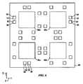
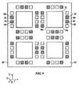
図3を参照すると、テンプレート18の平面図が示される。より具体的には、テンプレート18のモールド20が、ダイ60a〜60dとして示す複数のダイ60を備えるように示されている。しかし、さらなる実施形態では、モールド20は、任意の数のダイ、すなわち、2個の、4個の、6個の、8個の、又は9個のダイを備えてもよい。さらに、ダイ60a〜60dはそれぞれ、内部に形成された実質的に同じレリーフ構造61を有してもよい。そのために、モールド20のダイ60の形成が、電子ビーム・リソグラフィを使用して行われてもよい。しかし、電子ビーム・リソグラフィを使用することは、とりわけ、好ましくない場合がある、テンプレート18の形成時間の増加をもたらす可能性があるためである。その結果、モールド20のダイ60の形成時間を最小にする方法が、以下で述べられる。 Referring to FIG. 3, a plan view of
図3〜5を参照すると、第1の実施形態では、モールド20のダイ60を形成する方法が示される。より具体的には、ステップ100にて、マスタ・テンプレート62が、電子ビーム・リソグラフィを使用して形成される。マスタ・テンプレート62は、セクション64a〜64dとして示す複数のセクション64を備える。しかし、さらなる実施形態では、マスタ・テンプレート62は、任意の数のセクション64、すなわち、2個の、4個の、6個の、8個の、又は9個のセクションを備えてもよい。セクション64の各セクションは、ストリート66によってセクション64の隣接するセクションから分離されている。さらに、セクション64はそれぞれは、ストリート70によってマスタ・テンプレート62の外周68から分離されている。 3-5, in a first embodiment, a method for forming a die 60 of a
セクション64のうちのあるセクションは、内部に形成されたレリーフ・パターン74を有するメサ72を備えている。図示するように、メサ72は、セクション64aに配置されている。しかし、さらなる実施形態では、メサ72は、セクション64のうちの任意のセクションに配置されてもよい。メサ72は、側面76a、76b、76c、76dを有し、側面76aは側面76cに対向して配置され、側面76bは側面76dに対向して配置される。ある例では、マスタ・テンプレート62は、4mm以上の厚さを有してもよい。 One of the sections 64 includes a
マスタ・テンプレート62は、さらに、複数のアライメント形成領域78とテンプレート・アライメント・マーク80を備えいる。アライメント形成領域78とテンプレート・アライメント・マーク80は、ストリート66、70内に配置される。さらなる実施形態では、アライメント形成領域78とテンプレート・アライメント・マーク80は、複数のメサ上に配置されてもよい。なお、さらなる実施形態では、アライメント形成領域78は、チェッカボード形成アライメント・マークからなり、テンプレート・アライメント・マーク80は、グレーティング・アライメント・マークからなる。なおさらなる実施形態では、テンプレート・アライメント・マーク80は、実質的に平坦である。 The
第1パターン82aである、アライメント形成領域78とテンプレート・アライメント・マーク80の第1部分集合がメサ72に隣接して配置されている。図示するように、側面76a、76b、76c、76dのそれぞれのすぐ近くに、2個のアライメント形成領域78と2個のテンプレート・アライメント・マーク80が配置されている。しかし、他の実施形態では、任意の数のアライメント形成領域78とテンプレート・アライメント・マーク80が、側面76a、76b、76c、76dのすぐ近くに配置されてもよい。 A first subset of the
マスタ・テンプレート62は、さらに、マスタ・テンプレート62の残りのセクション64のすぐ近くでストリート66と70内に配置されたアライメント形成領域78とテンプレート・アライメント・マーク80を備える。より具体的には、アライメント形成領域78とテンプレート・アライメント・マーク80の第2、第3、第4の部分集合が、それぞれ、セクション64b、64c、64dのすぐ近くでストリート66、70内に配置されており、それぞれ、第2パターン82b、第3パターン82c、第4パターン82dとされる。第1パターン82aは、第3パターン82cに実質的に同じで、第2パターン82bは、第4パターン82dに実質的に同じである。一方、第1と第3パターン82a、82cは、第2と第4パターン82b、82dと異なっている。 The
図4〜6を参照すると、ステップ102にて、ポリマ材料34は、液滴分配、スピンコーティング、ディップ・コーティング、化学気相堆積(CVD)、物理気相堆積(PVD)、薄膜堆積、厚膜堆積などによって、中間基板84上に分配される。より具体的には、中間基板84は、フィールド86a〜86dとして示される複数のフィールド86を備えている。しかし、さらなる実施形態では、中間基板84は、任意の数のフィールド86、すなわち、2個の、4個の、6個の、8個の、又は9個のフィールドを備えてもよい。本例では、中間基板84のフィールド86の数は、マスタ・テンプレート62のセクション64の数と実質的に同じである。その結果、ポリマ材料34は、フィールド86a上に分配される。さらに、ポリマ材料34は、フィールド86a〜86dの外側にある複数の領域88上に分配されてもよい。ある例では、中間基板84は、0.05mm〜3mmの範囲の厚さを有している。 Referring to FIGS. 4-6, at
ステップ104にて、マスタ・テンプレート62と中間基板84との間、より具体的には、フィールド86aとメサ72との間に、所望の空間関係が得られる。さらに、ステップ104にて、フィールド86aのポリマ材料34は、中間基板84のフィールド86aとマスタ・テンプレート62のメサ72との間の所望の容積を充填し、また、領域88のポリマ材料34は、基板の領域88とマスタ・テンプレート62のアライメント形成領域78との間の所望の容積を充填する。 In
ステップ106にて、中間基板84のフィールド86aと領域88上に分配されたポリマ材料34は、固化し、及び/又は、架橋結合し、マスタ・テンプレート62のメサ72は、フィールド86a上に分配されたポリマ材料34から分離され、パターン化層90aが形成され、また、領域88上に分配されたポリマ材料34から分離され、基板アライメント・マークが形成される。中間基板84が、実質的にマスタ・テンプレート62の厚さ未満の厚さを有する結果として、分離力が最小になり、それが望ましい。 At
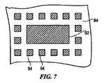
図7を参照すると、さらなる実施形態では、基板アライメント・マーク92はそれぞれ、さらに、像配置計量マーク94を備えている。像配置計量マーク94は、知られている像配置システム又は像位置合わせシステム、例えば、イリノイ州バノックバーン(Bannockburn, Illinois)のLeica Microsystemsから入手可能なLMS IPROを使用して測定される。 Referring to FIG. 7, in a further embodiment, each
図4、5、8を参照すると、ステップ108にて、ポリマ材料34は、図6及びステップ102に関して先に述べた方法のうちの任意の方法において、フィールド86b上に分配される。 Referring to FIGS. 4, 5, and 8, at
ステップ110にて、マスタ・テンプレート62のテンプレート・アライメント・マーク80と中間基板84の基板アライメント・マーク92との間で所望の空間関係が得られ、それにより、マスタ・テンプレート62と中間基板84との間に、より具体的には、本例では、フィールド86bとメサ72との間に、所望の空間関係が得られる。テンプレート・アライメント・マーク80と基板アライメント・マーク92との間の所望の空間関係は、テンプレート・アライメント・マーク80と基板アライメント・マーク92が重なってもよい。しかし、他の実施形態では、テンプレート・アライメント・マーク80と基板アライメント・マーク92は、所望の量だけ、x−y平面内でずれて、アライメント形成領域78とテンプレート・アライメント・マーク80の第1、第2、第3、第4のパターン82a、82b、82c、82dの間の変動を補償する。 At
テンプレート・アライメント・マーク80と基板アライメント・マーク92との間のアライメントは、参照により本明細書に組み込まれる、「Interferometric Analysis for the Manufacture of Nano−Scale Devices」という名称の米国特許出願第11/000,331号に記載されるアライメント・システムを使用して決定されてもよい。さらに、ステップ110にて、フィールド86bのポリマ材料34は、中間基板84のフィールド86bとマスタ・テンプレート62のメサ72との間の所望の容積を充填する。 The alignment between the
ステップ112にて、中間基板84のフィールド86b上に分配されたポリマ材料34は、固化し、及び/又は、架橋結合し、マスタ・テンプレート62のメサ72は、中間基板84上に分配されたポリマ材料34から分離され、フィールド86b上にパターン化層90bが形成される。 At
図4、5、9を参照すると、ステップ114にて、ポリマ材料34は、図6及びステップ102に関して先に述べた方法のうちの任意の方法において、フィールド86c上に分配される。 Referring to FIGS. 4, 5, and 9, at
ステップ116にて、マスタ・テンプレート62のテンプレート・アライメント・マーク80と中間基板84の基板アライメント・マーク92との間で所望の空間関係が得られ、それにより、マスタ・テンプレート62と中間基板84との間に、より具体的には、本例では、フィールド86cとメサ72との間に、所望の空間関係が得られる。その結果、マスタ・テンプレート62のテンプレート・アライメント・マーク80と基板アライメント・マーク92との間で所望の空間関係を得るために、マスタ・テンプレート62は、z軸を中心に回転する、より具体的には、中間基板84に対して180°回転する。結果として、テンプレート・アライメント・マーク80と基板アライメント・マーク92との間に、所望の空間関係が得られる。さらに、ステップ116にて、フィールド86cのポリマ材料34は、中間基板84のフィールド86cとマスタ・テンプレート62のメサ72との間の所望の容積を充填する。さらなる実施形態では、マスタ・テンプレート62は、中間基板84のフィールド86c上にポリマ材料34を分配する前に、回転する。 At
ステップ118にて、中間基板84のフィールド86c上に分配されたポリマ材料34は、固化し、及び/又は、架橋結合し、マスタ・テンプレート62のメサ72は、フィールド86a上に分配されたポリマ材料34から分離され、パターン化層90cが形成される。 At
図4、5を参照すると、ステップ120にて、ステップ108、110、112が、中間基板84のフィールド86dに対して繰り返され、フィールド86d上にパターン化層90dが形成される。さらなる実施形態では、ステップ108、110、112は、中間基板84の任意の数のフィールド86について、繰り返される。 4 and 5, in
図4、5、10を参照すると、フィールド86a、86b、86c、86d上に、それぞれ、パターン化層90a、90b、90c、90dを形成した後、中間基板84を使用して、最終基板96内にパターンを形成する。より具体的には、ステップ122にて、ポリマ材料34が、ステップ102及び図6に関して先に述べた方法のうちの任意の方法を使用して、最終基板96上に分配される。最終基板96は、フィールド98a〜98dとして示す複数のフィールド98を備えている。しかし、さらなる実施形態では、最終基板96は、任意の数のフィールド98、すなわち、2個の、4個の、6個の、8個の、又は9個のフィールドを備えてもよい。本実施形態では、最終基板96のフィールド98の数は、中間基板84のフィールド86の数と実質的に同じである。その結果、ポリマ材料34は、最終基板96のフィールド98上に分配される。ある例では、最終基板96は、4mm以上の厚さを有している。 Referring to FIGS. 4, 5, and 10, after forming
ステップ124にて、中間基板84と最終基板96との間で所望の空間関係が得られ、それにより、最終基板96上のポリマ材料34は、中間基板84と最終基板96との間の所望の容積を充填する。 At
ステップ126にて、最終基板96上に分配されたポリマ材料34は、固化し、及び/又は、架橋結合し、中間基板84は、最終基板96上に分配されたポリマ材料34から分離され、フィールド98のそれぞれにおいて複数のパターン化層99が形成され、このとき、パターン化層99はそれぞれ、モールド20のダイ60と実質的に同じであり、したがって、最終基板96は、テンプレート18と実質的に同じである。 At
図4〜6を参照すると、第2の実施形態では、単一パターニング・ステップで、マスタ・テンプレート62からテンプレート18を形成することが望ましい場合がある。その結果、中間基板84のフィールド86上に設けられたパターン化層99はそれぞれ、モールド20のダイ60と実質的に同じであり、したがって、中間基板84は、テンプレート18と実質的に同じである。本例では、マスタ・テンプレート62は約2.29mmの厚さを有し、中間基板84は6.35mmの厚さを有する。 4-6, in the second embodiment, it may be desirable to form the
図11を参照すると、なおさらなる実施形態では、基板アライメント・マーク92は、別個のステップにおいて、中間基板84上に形成される。より具体的には、基板アライメント・マーク92は、中間基板84上にパターン化層90を形成する前に、中間基板84上に形成される。その結果、基板アライメント・マーク92は、参照により本明細書に組み込まれる、a)オランダのASMLから入手可能な913nmスキャナ・リソグラフィ・ツールなどの、正確なグローバル干渉法を用いる光学リソグラフィ・ツール、又は、b)http://www.sciencedaily.com/releases/2004/02/040203233840.htmに記載されるNanorulerなどのエクセル干渉法を用いる光学リソグラフィ・ツールを使用して形成される。結果として、中間基板84のフィールド86の間のアライメント、すなわち、フィールド−フィールド・アライメントが得られる。 Referring to FIG. 11, in yet a further embodiment, the
その結果、図3、5、6を参照すると、上述したように、モールド20は、モールド20に関連する4個のダイを有している。しかし、先に述べたように、モールド20は、モールド20に関連する任意の数のダイを有してもよく、したがって、マスタ・テンプレート62、中間基板84、最終基板96は、相応してスケーリングされる。図12に示すように、マスタ・テンプレート62は、マスタ・テンプレート62に関連する9個のセクション64を有してもよい。その結果、マスタ・テンプレート62のセクション64はそれぞれ、アライメント形成領域78とアライメント形成領域78のすぐ近くのテンプレート・アライメント・マーク80のパターンを有し、より具体的は、セクション64のそれぞれのセクションは、セクション64の周囲のセクションのアライメント形成領域78とテンプレート・アライメント・マーク80のパターンと異なるアライメント形成領域78とテンプレート・アライメント・マーク80のパターンを有してもよい。より具体的には、セクション64a、64c、64e、64g、64iは、アライメント形成領域78とアライメント形成領域78のすぐ近くのテンプレート・アライメント・マーク80の第5パターンを有し、セクション64b、64d、64f、64hは、アライメント形成領域78とアライメント形成領域78のすぐ近くのテンプレート・アライメント・マーク80の第6パターンを有し、このとき、アライメント形成領域78とテンプレート・アライメント・マーク80の第5パターンは、図5に関して先に述べた第1パターンと実質的に同じであり、アライメント形成領域78とテンプレート・アライメント・マーク80の第6パターンは、図5に関して先に述べた第3パターンと実質的に同じである。さらに、セクション64e、64g、64iはそれぞれ、セクション64cのパターニングと類似の上述した方法でパターン化され、セクション64fと64hはそれぞれ、セクション64bと64dのパターニングと類似の上述した方法でパターン化される。 As a result, referring to FIGS. 3, 5, 6, as described above, the
さらに、上述した方法のうちの任意の方法において形成されるテンプレート18に存在する機械的歪を最小にすることが望ましい。そのために、マスタ・テンプレート62、中間基板84、最終基板96は、実質的に平坦である。より具体的には、マスタ・テンプレート62、中間基板84、最終基板96は、パターニング領域にわたって、100nm以下の、好ましくは50nm以下の、好ましくは20nm以下の、さらに好ましくは10nm以下の平坦度を有している。上述した機械的歪をさらに最小にするため、とりわけ、像配置誤差を最小にするため、中間基板84は、マスタ・テンプレート62に一致する。そのために、マスタ・テンプレート62、中間基板84、最終基板96は、図1に関して上述した基板チャック14と類似のチャック上に配置される。マスタ・テンプレート62、中間基板84、最終基板96の形状は、参照により本明細書に組み込まれる、XYステージ(図示せず)に結合した空気圧力計システム(図示せず)、XYステージ(図示せず)に結合したレーザ距離センサ・システム(図示せず)、又は、http://www.zygo.com/?/products/metrology.htmに記載されるフル・フィールド3Dプロファイラ(図示せず)を使用して決定されてもよい。さらに、マスタ・テンプレート62、中間基板84、最終基板96はそれぞれ、実質的に同じ材料から形成されてもよく、材料は、溶融シリカ及び超低膨張ガラスを含むが、それに限定されない。さらに、マスタ・テンプレート62と、中間基板84と、最終基板96との間の温度差は、0.05℃未満、好ましくは0.01℃未満、さらに好ましくは0.001℃未満である。 Furthermore, it is desirable to minimize mechanical strain present in the
上述した方法のうちの任意の方法において形成される誤差を、防止できない場合、最小にするために、上述した第1の実施形態では、マスタ・テンプレート62は、図1に関して上述したアクチュエーション・システム58と類似の、マスタ・テンプレート62に結合したアクチュエーション・システムを有する。上述した第2の実施形態では、最終基板96は、図1に関して上述したアクチュエーション・システム58と類似の、最終基板96に結合したアクチュエーション・システムを有する。 In order to minimize the errors formed in any of the methods described above if they cannot be prevented, in the first embodiment described above, the
上述した方法は、フォトリソグラフィ用のフォトマスクの形成時に同様に使用できる。フォトマスクは、通常、4×である(フォトマスクのレリーフ・パターンは、基板上に形成される所望のフィーチャのサイズの5倍である)。KrF(248nm)レーザ及びArF(193nm)レーザを用いるフォトリソグラフィで使用される最新のフォトマスクは、さらに、主要なフィーチャより小さいサブ解像度フィーチャを有している。これらのサブ解像度はまた、光近接効果補正フィーチャ又はレチクル増強フィーチャとして知られている。サブ解像度フィーチャは印刷されない。サブ解像度フィーチャは、主要なフィーチャの品質を増強するように設計される。上述したように、主要なフィーチャは4×である。例えば、ウェハ上で50nmのサイズのフィーチャの場合、主要なフォトマスク・フィーチャは200nmである。サブ解像度フィーチャは、1×以下と同程度に小さいか、又は、4×に近い程度に大きくてもよい。通常、小さなサブ解像度フィーチャは、約1.5×であり、50nmウェハ・フィーチャの場合、これは、フォトマスク上で75nmに変換される。4×のフォトマスクは、例えば、25mm×35mmウェハ・フィールド・サイズの場合、サイズ100mm×100mmであり、26mm×33mmウェハ・フィールド・サイズの場合、サイズ104mm×132mmである。これらのフィールドは、通常、フィールド内に、2個の、4個の、6個の、又はそれ以上のダイを有し、ダイはそれぞれ、実質的に同じパターン要件を有する。こうして、上述した方法は、フォトリソグラフィ用のフォトマスクの形成時に同様に使用される。 The above-described method can be similarly used when forming a photomask for photolithography. A photomask is typically 4x (the photomask relief pattern is five times the size of the desired feature to be formed on the substrate). Modern photomasks used in photolithography using KrF (248 nm) and ArF (193 nm) lasers also have sub-resolution features that are smaller than the main features. These sub-resolutions are also known as optical proximity correction features or reticle enhancement features. Sub-resolution features are not printed. Sub-resolution features are designed to enhance the quality of key features. As mentioned above, the main feature is 4x. For example, for a 50 nm size feature on a wafer, the main photomask feature is 200 nm. The sub-resolution feature may be as small as 1 × or less, or as large as close to 4 ×. Typically, a small sub-resolution feature is about 1.5 ×, and for a 50 nm wafer feature this is converted to 75 nm on the photomask. The 4 × photomask is, for example, a size of 100 mm × 100 mm for a 25 mm × 35 mm wafer field size and a size of 104 mm × 132 mm for a 26 mm × 33 mm wafer field size. These fields typically have two, four, six, or more dies in the field, and each die has substantially the same pattern requirements. Thus, the above-described method is similarly used when forming a photomask for photolithography.
上述した本発明の実施形態が例示的である。本発明の範囲内に留まったままで、先に引用した開示に対して、多くの変更及び修正が行われてもよい。したがって、本発明の範囲は、先の説明によって制限されるべきではなく、代わりに、添付特許請求の範囲の等価物の全範囲と一緒に、添付特許請求の範囲を参照して決められるべきである。 The above-described embodiments of the present invention are exemplary. Many changes and modifications may be made to the above cited disclosure while remaining within the scope of the invention. Accordingly, the scope of the invention should not be limited by the foregoing description, but instead should be determined with reference to the appended claims, along with their full scope of equivalents. is there.
Claims (18)
Translated fromJapanese前記基板の前記第1フィールド、及び、前記第1と第2フィールドの外側にある前記基板の複数の領域上に材料を分配すること、
前記基板の前記第1フィールド上の前記材料内にパターン化層を形成し、一方、同時に、前記テンプレートの前記第2の領域における前記第2のパターンを形成するアライメント形成領域に重なった前記基板の前記複数の領域内の前記材料を用いて複数の基板アライメント・マークを形成するために、前記レリーフ・パターンと前記基板の前記第1フィールドとの間の所望の空間関係が得られるように、前記レリーフ・パターンと前記基板とを配置すること、
前記基板の前記第2フィールド上に材料を分配すること、
前記基板の前記第2フィールド上の前記材料内にパターン化層を形成するように、前記レリーフ・パターンと前記基板の前記第2フィールドとの間の所望の空間関係が得られるように、テンプレート・アライメント・マークの前記第1の部分集合と前記複数の基板アライメント・マークとの間の所望の空間関係を得るように前記レリーフ・パターンと前記基板とを配置することを含む方法。A template having a plurality ofregions , the firstregion having arelief pattern , an alignment forming region for forming the firstpattern, and a first subset of the plurality of template alignment marks;Region 2 has an alignment formation region for forming a second pattern and a second subset of a plurality of template alignment marks, wherein the first pattern corresponds to the second pattern, depending onthe template In a method of patterning a substrate comprising a first field and a second field,
Distributing material over the first field of the substrate and a plurality of regions of the substrate that are outside the first and second fields;
Forming a patternedlayer in the material on the first field of the substrate while simultaneously overlapping thealignment formation region forming the second pattern in the second region of the template In order to form a plurality of substrate alignment marks using the material in the plurality of regions, the desired spatial relationship between therelief pattern and the first field of the substrate is obtained. Arranging therelief pattern and the substrate;
Dispensing material onto the second field of the substrate;
In order to obtain a desired spatial relationship between therelief pattern and the second field of the substrate so as to form a patternedlayer in the material on the second field of the substrate. Disposing therelief pattern and the substrate to obtain a desired spatial relationship between the first subset of alignment marks and the plurality of substrate alignment marks.
Applications Claiming Priority (3)
| Application Number | Priority Date | Filing Date | Title |
|---|---|---|---|
| US78880606P | 2006-04-03 | 2006-04-03 | |
| US60/788,806 | 2006-04-03 | ||
| PCT/US2007/008434WO2007117524A2 (en) | 2006-04-03 | 2007-04-03 | Method of concurrently patterning a substrate having a plurality of fields and alignment marks |
Publications (2)
| Publication Number | Publication Date |
|---|---|
| JP2009532909A JP2009532909A (en) | 2009-09-10 |
| JP5306989B2true JP5306989B2 (en) | 2013-10-02 |
Family
ID=38581610
Family Applications (1)
| Application Number | Title | Priority Date | Filing Date |
|---|---|---|---|
| JP2009504287AExpired - Fee RelatedJP5306989B2 (en) | 2006-04-03 | 2007-04-03 | Method for simultaneously patterning a substrate having a plurality of fields and alignment marks |
Country Status (5)
| Country | Link |
|---|---|
| US (2) | US7780893B2 (en) |
| JP (1) | JP5306989B2 (en) |
| KR (1) | KR20090003153A (en) |
| TW (1) | TW200801794A (en) |
| WO (1) | WO2007117524A2 (en) |
Families Citing this family (77)
| Publication number | Priority date | Publication date | Assignee | Title |
|---|---|---|---|---|
| US7162035B1 (en) | 2000-05-24 | 2007-01-09 | Tracer Detection Technology Corp. | Authentication method and system |
| US7179079B2 (en)* | 2002-07-08 | 2007-02-20 | Molecular Imprints, Inc. | Conforming template for patterning liquids disposed on substrates |
| US7019819B2 (en) | 2002-11-13 | 2006-03-28 | Molecular Imprints, Inc. | Chucking system for modulating shapes of substrates |
| US7442336B2 (en)* | 2003-08-21 | 2008-10-28 | Molecular Imprints, Inc. | Capillary imprinting technique |
| US20060062922A1 (en) | 2004-09-23 | 2006-03-23 | Molecular Imprints, Inc. | Polymerization technique to attenuate oxygen inhibition of solidification of liquids and composition therefor |
| US7630067B2 (en)* | 2004-11-30 | 2009-12-08 | Molecular Imprints, Inc. | Interferometric analysis method for the manufacture of nano-scale devices |
| US20070231421A1 (en) | 2006-04-03 | 2007-10-04 | Molecular Imprints, Inc. | Enhanced Multi Channel Alignment |
| US8999218B2 (en)* | 2005-06-06 | 2015-04-07 | Canon Kabushiki Kaisha | Process for producing member having pattern, pattern transfer apparatus, and mold |
| US7906058B2 (en) | 2005-12-01 | 2011-03-15 | Molecular Imprints, Inc. | Bifurcated contact printing technique |
| US7670530B2 (en) | 2006-01-20 | 2010-03-02 | Molecular Imprints, Inc. | Patterning substrates employing multiple chucks |
| MY144847A (en) | 2005-12-08 | 2011-11-30 | Molecular Imprints Inc | Method and system for double-sided patterning of substrates |
| US8850980B2 (en)* | 2006-04-03 | 2014-10-07 | Canon Nanotechnologies, Inc. | Tessellated patterns in imprint lithography |
| US7802978B2 (en)* | 2006-04-03 | 2010-09-28 | Molecular Imprints, Inc. | Imprinting of partial fields at the edge of the wafer |
| US8142850B2 (en)* | 2006-04-03 | 2012-03-27 | Molecular Imprints, Inc. | Patterning a plurality of fields on a substrate to compensate for differing evaporation times |
| US8012395B2 (en) | 2006-04-18 | 2011-09-06 | Molecular Imprints, Inc. | Template having alignment marks formed of contrast material |
| US7547398B2 (en) | 2006-04-18 | 2009-06-16 | Molecular Imprints, Inc. | Self-aligned process for fabricating imprint templates containing variously etched features |
| US8215946B2 (en) | 2006-05-18 | 2012-07-10 | Molecular Imprints, Inc. | Imprint lithography system and method |
| TW200842934A (en)* | 2006-12-29 | 2008-11-01 | Molecular Imprints Inc | Imprint fluid control |
| US20090014917A1 (en)* | 2007-07-10 | 2009-01-15 | Molecular Imprints, Inc. | Drop Pattern Generation for Imprint Lithography |
| US7837907B2 (en)* | 2007-07-20 | 2010-11-23 | Molecular Imprints, Inc. | Alignment system and method for a substrate in a nano-imprint process |
| US8119052B2 (en)* | 2007-11-02 | 2012-02-21 | Molecular Imprints, Inc. | Drop pattern generation for imprint lithography |
| US20090148619A1 (en)* | 2007-12-05 | 2009-06-11 | Molecular Imprints, Inc. | Controlling Thickness of Residual Layer |
| US20090147237A1 (en)* | 2007-12-05 | 2009-06-11 | Molecular Imprints, Inc. | Spatial Phase Feature Location |
| US8012394B2 (en)* | 2007-12-28 | 2011-09-06 | Molecular Imprints, Inc. | Template pattern density doubling |
| US8361371B2 (en)* | 2008-02-08 | 2013-01-29 | Molecular Imprints, Inc. | Extrusion reduction in imprint lithography |
| US20090212012A1 (en)* | 2008-02-27 | 2009-08-27 | Molecular Imprints, Inc. | Critical dimension control during template formation |
| US7995196B1 (en) | 2008-04-23 | 2011-08-09 | Tracer Detection Technology Corp. | Authentication method and system |
| US9005848B2 (en)* | 2008-06-17 | 2015-04-14 | Photronics, Inc. | Photomask having a reduced field size and method of using the same |
| US20100022036A1 (en)* | 2008-07-25 | 2010-01-28 | Ikuo Yoneda | Method for forming pattern, and template |
| JP2010080630A (en)* | 2008-09-25 | 2010-04-08 | Canon Inc | Stamping device and method of manufacturing article |
| TW201022017A (en)* | 2008-09-30 | 2010-06-16 | Molecular Imprints Inc | Particle mitigation for imprint lithography |
| US20100092599A1 (en)* | 2008-10-10 | 2010-04-15 | Molecular Imprints, Inc. | Complementary Alignment Marks for Imprint Lithography |
| US20100096764A1 (en)* | 2008-10-20 | 2010-04-22 | Molecular Imprints, Inc. | Gas Environment for Imprint Lithography |
| US8512797B2 (en)* | 2008-10-21 | 2013-08-20 | Molecular Imprints, Inc. | Drop pattern generation with edge weighting |
| US8586126B2 (en) | 2008-10-21 | 2013-11-19 | Molecular Imprints, Inc. | Robust optimization to generate drop patterns in imprint lithography which are tolerant of variations in drop volume and drop placement |
| US8345242B2 (en)* | 2008-10-28 | 2013-01-01 | Molecular Imprints, Inc. | Optical system for use in stage control |
| US20100112310A1 (en)* | 2008-10-30 | 2010-05-06 | Molecular Imprints, Inc. | Substrate Patterning |
| US8432548B2 (en)* | 2008-11-04 | 2013-04-30 | Molecular Imprints, Inc. | Alignment for edge field nano-imprinting |
| US8231821B2 (en)* | 2008-11-04 | 2012-07-31 | Molecular Imprints, Inc. | Substrate alignment |
| US8529778B2 (en)* | 2008-11-13 | 2013-09-10 | Molecular Imprints, Inc. | Large area patterning of nano-sized shapes |
| WO2010111307A1 (en)* | 2009-03-23 | 2010-09-30 | Intevac, Inc. | A process for optimization of island to trench ratio in patterned media |
| CN101870151A (en) | 2009-04-27 | 2010-10-27 | 鸿富锦精密工业(深圳)有限公司 | Optical element manufacturing method and imprint mold |
| US9005849B2 (en)* | 2009-06-17 | 2015-04-14 | Photronics, Inc. | Photomask having a reduced field size and method of using the same |
| JP5809409B2 (en)* | 2009-12-17 | 2015-11-10 | キヤノン株式会社 | Imprint apparatus and pattern transfer method |
| WO2011097514A2 (en) | 2010-02-05 | 2011-08-11 | Molecular Imprints, Inc. | Templates having high contrast alignment marks |
| JP5699461B2 (en)* | 2010-07-02 | 2015-04-08 | 住友電気工業株式会社 | Nanoimprint mold |
| JP5759003B2 (en) | 2010-09-02 | 2015-08-05 | エーファウ・グループ・ゲーエムベーハー | Stamping tool, device and method for manufacturing lens wafers |
| EP2618978B1 (en) | 2010-09-24 | 2016-11-09 | Canon Nanotechnologies, Inc. | High contrast alignment marks through multiple stage imprinting |
| US9643366B2 (en) | 2010-10-26 | 2017-05-09 | Ev Group Gmbh | Method and device for producing a lens wafer |
| KR102046933B1 (en) | 2010-11-05 | 2019-11-20 | 캐논 나노테크놀로지즈 인코퍼레이티드 | Patterning of non-convex shaped nanostructures |
| JP5709558B2 (en)* | 2011-02-01 | 2015-04-30 | キヤノン株式会社 | Inspection method, imprint apparatus, and article manufacturing method |
| US8967992B2 (en) | 2011-04-25 | 2015-03-03 | Canon Nanotechnologies, Inc. | Optically absorptive material for alignment marks |
| CN102591142B (en)* | 2012-02-29 | 2013-03-27 | 青岛理工大学 | Nano-imprinting device and method for patterning sapphire substrate |
| TWI455833B (en)* | 2012-02-29 | 2014-10-11 | Microjet Technology Co Ltd | 3d image printing apparatus and 3d printing correction method thereof |
| JP6071221B2 (en)* | 2012-03-14 | 2017-02-01 | キヤノン株式会社 | Imprint apparatus, mold, imprint method, and article manufacturing method |
| WO2014145036A1 (en)* | 2013-03-15 | 2014-09-18 | The Trustees Of Princeton University | Rapid and sensitive analyte measurement assay |
| JP5723337B2 (en)* | 2012-09-07 | 2015-05-27 | 株式会社東芝 | Pattern forming method and pattern forming apparatus |
| US9646896B2 (en)* | 2013-07-12 | 2017-05-09 | Taiwan Semiconductor Manufacturing Co., Ltd. | Lithographic overlay sampling |
| JP2015146412A (en)* | 2014-02-04 | 2015-08-13 | 株式会社東芝 | Imprint template and manufacturing method thereof |
| KR102154561B1 (en)* | 2014-04-01 | 2020-09-10 | 다이니폰 인사츠 가부시키가이샤 | Imprinting mold and imprinting method |
| JP6361303B2 (en)* | 2014-06-13 | 2018-07-25 | 大日本印刷株式会社 | Imprint mold and imprint apparatus |
| JP5874782B2 (en)* | 2014-06-30 | 2016-03-02 | 信越化学工業株式会社 | Mold substrate and mold substrate inspection method |
| JP6385177B2 (en)* | 2014-07-16 | 2018-09-05 | キヤノン株式会社 | Mold, imprint apparatus, and article manufacturing method |
| JP5900589B2 (en)* | 2014-12-12 | 2016-04-06 | 大日本印刷株式会社 | Imprint mold, alignment method, imprint method, and imprint apparatus |
| JP2016134441A (en)* | 2015-01-16 | 2016-07-25 | キヤノン株式会社 | Imprint apparatus, imprint method, and article manufacturing method |
| JP2017152673A (en)* | 2015-11-05 | 2017-08-31 | ボード・オブ・リージェンツ, ジ・ユニバーシティー・オブ・テキサス・システム | Multi-field overlay control in jet and flash imprint lithography |
| US9975364B2 (en)* | 2016-07-12 | 2018-05-22 | Hewlett-Packard Development Company, L.P. | Determining deformations of slices of an image |
| US10429743B2 (en) | 2017-11-30 | 2019-10-01 | International Business Machines Corporation | Optical mask validation |
| US10650111B2 (en) | 2017-11-30 | 2020-05-12 | International Business Machines Corporation | Electrical mask validation |
| JP7089375B2 (en)* | 2018-02-19 | 2022-06-22 | キヤノン株式会社 | Flattening device |
| JP6540848B2 (en)* | 2018-03-16 | 2019-07-10 | 大日本印刷株式会社 | Template for nanoimprint |
| CN110416103B (en)* | 2018-04-28 | 2021-09-28 | 上海微电子装备(集团)股份有限公司 | Residual gum standard tablet and preparation method thereof |
| CN110687759B (en)* | 2018-07-06 | 2021-04-02 | 上海微电子装备(集团)股份有限公司 | Mask plate and bonding alignment method |
| JP2020035924A (en)* | 2018-08-30 | 2020-03-05 | キオクシア株式会社 | Original |
| KR102666843B1 (en)* | 2018-08-31 | 2024-05-21 | 삼성디스플레이 주식회사 | Master stamp for nano imprint and method of manufacturing of the smae |
| JP7361538B2 (en)* | 2018-09-10 | 2023-10-16 | キヤノン株式会社 | Imprint method and article manufacturing method |
| CN116056866A (en)* | 2020-08-03 | 2023-05-02 | 应用材料公司 | Apparatus and method for making seamless soft impressions |
Family Cites Families (288)
| Publication number | Priority date | Publication date | Assignee | Title |
|---|---|---|---|---|
| GB1183056A (en) | 1966-11-29 | 1970-03-04 | Bp Chemicals U K Ltd Formerly | Metering Process for Dispensing Measured Quantities of Liquefied Gas |
| US3783520A (en) | 1970-09-28 | 1974-01-08 | Bell Telephone Labor Inc | High accuracy alignment procedure utilizing moire patterns |
| US4022855A (en) | 1975-03-17 | 1977-05-10 | Eastman Kodak Company | Method for making a plastic optical element having a gradient index of refraction |
| FR2325018A1 (en) | 1975-06-23 | 1977-04-15 | Ibm | INTERVAL MEASURING DEVICE FOR DEFINING THE DISTANCE BETWEEN TWO OR MORE FACES |
| US4208240A (en) | 1979-01-26 | 1980-06-17 | Gould Inc. | Method and apparatus for controlling plasma etching |
| US4326805A (en) | 1980-04-11 | 1982-04-27 | Bell Telephone Laboratories, Incorporated | Method and apparatus for aligning mask and wafer members |
| DE3022709A1 (en) | 1980-06-18 | 1982-01-07 | Felix Schoeller jr. GmbH & Co KG, 4500 Osnabrück | WATERPROOF PHOTOGRAPHIC PAPER AND METHOD FOR THE PRODUCTION THEREOF |
| US4576900A (en) | 1981-10-09 | 1986-03-18 | Amdahl Corporation | Integrated circuit multilevel interconnect system and method |
| DE3208081A1 (en) | 1982-03-06 | 1983-09-08 | Braun Ag, 6000 Frankfurt | METHOD FOR PRODUCING A SHEET-LIKE SHEAR FILM FOR AN ELECTRICALLY OPERATED DRY SHAVER WITH Raises On Its Face Facing The Skin |
| US4440804A (en) | 1982-08-02 | 1984-04-03 | Fairchild Camera & Instrument Corporation | Lift-off process for fabricating self-aligned contacts |
| US4490409A (en) | 1982-09-07 | 1984-12-25 | Energy Sciences, Inc. | Process and apparatus for decorating the surfaces of electron irradiation cured coatings on radiation-sensitive substrates |
| FR2538923A1 (en) | 1982-12-30 | 1984-07-06 | Thomson Csf | METHOD AND DEVICE FOR OPTICALLY ALIGNING PATTERNS IN TWO PLANS RECONCILED IN AN EXPOSURE APPARATUS COMPRISING A DIVERGENT RADIATION SOURCE |
| US4637904A (en) | 1983-11-14 | 1987-01-20 | Rohm And Haas Company | Process for molding a polymeric layer onto a substrate |
| US4512848A (en) | 1984-02-06 | 1985-04-23 | Exxon Research And Engineering Co. | Procedure for fabrication of microstructures over large areas using physical replication |
| US4908298A (en) | 1985-03-19 | 1990-03-13 | International Business Machines Corporation | Method of creating patterned multilayer films for use in production of semiconductor circuits and systems |
| EP0228671A1 (en) | 1985-12-23 | 1987-07-15 | General Electric Company | Method for the production of a coated substrate with controlled surface characteristics |
| DE3767317D1 (en) | 1986-02-13 | 1991-02-21 | Philips Nv | DIE FOR AN IMPRESSION PROCESS. |
| US4676868A (en) | 1986-04-23 | 1987-06-30 | Fairchild Semiconductor Corporation | Method for planarizing semiconductor substrates |
| US4737425A (en) | 1986-06-10 | 1988-04-12 | International Business Machines Corporation | Patterned resist and process |
| KR900004269B1 (en) | 1986-06-11 | 1990-06-18 | 가부시기가이샤 도시바 | Method and device for positioing 1st body and 2nd body |
| US4929083A (en) | 1986-06-19 | 1990-05-29 | Xerox Corporation | Focus and overlay characterization and optimization for photolithographic exposure |
| JPS6334108A (en) | 1986-07-30 | 1988-02-13 | Hitachi Ltd | Manufacturing method and device for optical disk substrate |
| JPS6376330A (en) | 1986-09-18 | 1988-04-06 | Oki Electric Ind Co Ltd | Manufacture of semiconductor device |
| FR2604553A1 (en) | 1986-09-29 | 1988-04-01 | Rhone Poulenc Chimie | RIGID POLYMER SUBSTRATE FOR OPTICAL DISC AND OPTICAL DISCS OBTAINED FROM THE SUBSTRATE |
| US4707218A (en) | 1986-10-28 | 1987-11-17 | International Business Machines Corporation | Lithographic image size reduction |
| JPH06104375B2 (en) | 1986-11-10 | 1994-12-21 | 松下電器産業株式会社 | Printing method |
| JP2823016B2 (en) | 1986-12-25 | 1998-11-11 | ソニー株式会社 | Method of manufacturing transmission screen |
| US6391798B1 (en) | 1987-02-27 | 2002-05-21 | Agere Systems Guardian Corp. | Process for planarization a semiconductor substrate |
| US5736424A (en) | 1987-02-27 | 1998-04-07 | Lucent Technologies Inc. | Device fabrication involving planarization |
| US6048799A (en) | 1987-02-27 | 2000-04-11 | Lucent Technologies Inc. | Device fabrication involving surface planarization |
| US4731155A (en) | 1987-04-15 | 1988-03-15 | General Electric Company | Process for forming a lithographic mask |
| US5028361A (en) | 1987-11-09 | 1991-07-02 | Takeo Fujimoto | Method for molding a photosensitive composition |
| US4936465A (en) | 1987-12-07 | 1990-06-26 | Zoeld Tibor | Method and apparatus for fast, reliable, and environmentally safe dispensing of fluids, gases and individual particles of a suspension through pressure control at well defined parts of a closed flow-through system |
| US5028366A (en) | 1988-01-12 | 1991-07-02 | Air Products And Chemicals, Inc. | Water based mold release compositions for making molded polyurethane foam |
| US4866307A (en) | 1988-04-20 | 1989-09-12 | Texas Instruments Incorporated | Integrated programmable bit circuit using single-level poly construction |
| US4862019A (en) | 1988-04-20 | 1989-08-29 | Texas Instruments Incorporated | Single-level poly programmable bit circuit |
| JPH0269936A (en) | 1988-07-28 | 1990-03-08 | Siemens Ag | Method for forming resin structures on semiconductor materials |
| US4921778A (en) | 1988-07-29 | 1990-05-01 | Shipley Company Inc. | Photoresist pattern fabrication employing chemically amplified metalized material |
| EP0355496A3 (en) | 1988-08-15 | 1990-10-10 | Sumitomo Heavy Industries Co., Ltd. | Position detector employing a sector fresnel zone plate |
| JP2546350B2 (en) | 1988-09-09 | 1996-10-23 | キヤノン株式会社 | Alignment device |
| US4964945A (en) | 1988-12-09 | 1990-10-23 | Minnesota Mining And Manufacturing Company | Lift off patterning process on a flexible substrate |
| US5110514A (en) | 1989-05-01 | 1992-05-05 | Soane Technologies, Inc. | Controlled casting of a shrinkable material |
| US4932358A (en) | 1989-05-18 | 1990-06-12 | Genus, Inc. | Perimeter wafer seal |
| US5053318A (en) | 1989-05-18 | 1991-10-01 | Shipley Company Inc. | Plasma processing with metal mask integration |
| CA2011927C (en) | 1989-06-02 | 1996-12-24 | Alan Lee Sidman | Microlithographic method for producing thick, vertically-walled photoresist patterns |
| US4919748A (en) | 1989-06-30 | 1990-04-24 | At&T Bell Laboratories | Method for tapered etching |
| JP2704001B2 (en) | 1989-07-18 | 1998-01-26 | キヤノン株式会社 | Position detection device |
| DE4031637C2 (en) | 1989-10-06 | 1997-04-10 | Toshiba Kawasaki Kk | Arrangement for measuring a displacement between two objects |
| US5362606A (en) | 1989-10-18 | 1994-11-08 | Massachusetts Institute Of Technology | Positive resist pattern formation through focused ion beam exposure and surface barrier silylation |
| US5073230A (en) | 1990-04-17 | 1991-12-17 | Arizona Board Of Regents Acting On Behalf Of Arizona State University | Means and methods of lifting and relocating an epitaxial device layer |
| US5003062A (en) | 1990-04-19 | 1991-03-26 | Taiwan Semiconductor Manufacturing Co. | Semiconductor planarization process for submicron devices |
| US5328810A (en) | 1990-05-07 | 1994-07-12 | Micron Technology, Inc. | Method for reducing, by a factor or 2-N, the minimum masking pitch of a photolithographic process |
| US5451435A (en) | 1990-06-18 | 1995-09-19 | At&T Corp. | Method for forming dielectric |
| DE4029912A1 (en) | 1990-09-21 | 1992-03-26 | Philips Patentverwaltung | METHOD FOR FORMING AT LEAST ONE TRENCH IN A SUBSTRATE LAYER |
| US5331371A (en) | 1990-09-26 | 1994-07-19 | Canon Kabushiki Kaisha | Alignment and exposure method |
| US5126006A (en) | 1990-10-30 | 1992-06-30 | International Business Machines Corp. | Plural level chip masking |
| US5072126A (en) | 1990-10-31 | 1991-12-10 | International Business Machines Corporation | Promixity alignment using polarized illumination and double conjugate projection lens |
| US5288436A (en) | 1990-11-06 | 1994-02-22 | Colloptics, Inc. | Methods of fabricating a collagen lenticule precursor for modifying the cornea |
| US5362940A (en) | 1990-11-09 | 1994-11-08 | Litel Instruments | Use of Fresnel zone plates for material processing |
| JP2796899B2 (en) | 1991-02-16 | 1998-09-10 | 住友重機械工業株式会社 | Illumination method for band light and multicolor light in a chromatic aberration double focus device |
| US5240878A (en) | 1991-04-26 | 1993-08-31 | International Business Machines Corporation | Method for forming patterned films on a substrate |
| US5212147A (en) | 1991-05-15 | 1993-05-18 | Hewlett-Packard Company | Method of forming a patterned in-situ high Tc superconductive film |
| FR2677043B1 (en) | 1991-05-29 | 1993-12-24 | Solems | METHOD, DEVICE AND APPARATUS FOR TREATING A SUBSTRATE WITH A LOW PRESSURE PLASMA. |
| EP0524759A1 (en) | 1991-07-23 | 1993-01-27 | AT&T Corp. | Device fabrication process |
| US5357122A (en) | 1991-09-05 | 1994-10-18 | Sony Corporation | Three-dimensional optical-electronic integrated circuit device with raised sections |
| JPH0580530A (en) | 1991-09-24 | 1993-04-02 | Hitachi Ltd | Production of thin film pattern |
| US5277749A (en) | 1991-10-17 | 1994-01-11 | International Business Machines Corporation | Methods and apparatus for relieving stress and resisting stencil delamination when performing lift-off processes that utilize high stress metals and/or multiple evaporation steps |
| US5263073A (en) | 1991-12-20 | 1993-11-16 | Board Of Supervisors Of Louisiana State University And Agricultural And Mechanical College | Scanning systems for high resolution E-beam and X-ray lithography |
| JP3074579B2 (en) | 1992-01-31 | 2000-08-07 | キヤノン株式会社 | Position shift correction method |
| JP2867194B2 (en) | 1992-02-05 | 1999-03-08 | 東京エレクトロン株式会社 | Processing device and processing method |
| US5204739A (en) | 1992-02-07 | 1993-04-20 | Karl Suss America, Inc. | Proximity mask alignment using a stored video image |
| US5244818A (en) | 1992-04-08 | 1993-09-14 | Georgia Tech Research Corporation | Processes for lift-off of thin film materials and for the fabrication of three dimensional integrated circuits |
| US5545367A (en) | 1992-04-15 | 1996-08-13 | Soane Technologies, Inc. | Rapid prototype three dimensional stereolithography |
| US5246880A (en) | 1992-04-27 | 1993-09-21 | Eastman Kodak Company | Method for creating substrate electrodes for flip chip and other applications |
| JP3157605B2 (en) | 1992-04-28 | 2001-04-16 | 東京エレクトロン株式会社 | Plasma processing equipment |
| EP0568478A1 (en) | 1992-04-29 | 1993-11-03 | International Business Machines Corporation | Darkfield alignment system using a confocal spatial filter |
| US5407763A (en)* | 1992-05-28 | 1995-04-18 | Ceridian Corporation | Mask alignment mark system |
| US5371822A (en) | 1992-06-09 | 1994-12-06 | Digital Equipment Corporation | Method of packaging and assembling opto-electronic integrated circuits |
| US5232874A (en) | 1992-06-22 | 1993-08-03 | Micron Technology, Inc. | Method for producing a semiconductor wafer having shallow and deep buried contacts |
| US5376810A (en) | 1992-06-26 | 1994-12-27 | California Institute Of Technology | Growth of delta-doped layers on silicon CCD/S for enhanced ultraviolet response |
| US5445195A (en) | 1992-07-15 | 1995-08-29 | Kim; Dae S. | Automatic computer-controlled liquid dispenser |
| US5601641A (en) | 1992-07-21 | 1997-02-11 | Tse Industries, Inc. | Mold release composition with polybutadiene and method of coating a mold core |
| US5250472A (en) | 1992-09-03 | 1993-10-05 | Industrial Technology Research Institute | Spin-on-glass integration planarization having siloxane partial etchback and silicate processes |
| US5431777A (en) | 1992-09-17 | 1995-07-11 | International Business Machines Corporation | Methods and compositions for the selective etching of silicon |
| TW227628B (en) | 1992-12-10 | 1994-08-01 | Samsung Electronics Co Ltd | |
| JP2821073B2 (en) | 1992-12-18 | 1998-11-05 | 松下電器産業株式会社 | Gap control device and gap control method |
| US6153886A (en) | 1993-02-19 | 2000-11-28 | Nikon Corporation | Alignment apparatus in projection exposure apparatus |
| DE69405451T2 (en) | 1993-03-16 | 1998-03-12 | Koninkl Philips Electronics Nv | Method and device for producing a structured relief image from cross-linked photoresist on a flat substrate surface |
| US5414514A (en) | 1993-06-01 | 1995-05-09 | Massachusetts Institute Of Technology | On-axis interferometric alignment of plates using the spatial phase of interference patterns |
| US5324683A (en) | 1993-06-02 | 1994-06-28 | Motorola, Inc. | Method of forming a semiconductor structure having an air region |
| JP2837063B2 (en) | 1993-06-04 | 1998-12-14 | シャープ株式会社 | Method of forming resist pattern |
| US6180239B1 (en) | 1993-10-04 | 2001-01-30 | President And Fellows Of Harvard College | Microcontact printing on surfaces and derivative articles |
| US5449117A (en) | 1993-10-04 | 1995-09-12 | Technical Concepts, L.P. | Apparatus and method for controllably dispensing drops of liquid |
| US5900160A (en) | 1993-10-04 | 1999-05-04 | President And Fellows Of Harvard College | Methods of etching articles via microcontact printing |
| US5512131A (en) | 1993-10-04 | 1996-04-30 | President And Fellows Of Harvard College | Formation of microstamped patterns on surfaces and derivative articles |
| US5776748A (en) | 1993-10-04 | 1998-07-07 | President And Fellows Of Harvard College | Method of formation of microstamped patterns on plates for adhesion of cells and other biological materials, devices and uses therefor |
| US6776094B1 (en) | 1993-10-04 | 2004-08-17 | President & Fellows Of Harvard College | Kit For Microcontact Printing |
| NL9401260A (en) | 1993-11-12 | 1995-06-01 | Cornelis Johannes Maria Van Ri | Membrane for microfiltration, ultrafiltration, gas separation and catalysis, method for manufacturing such a membrane, mold for manufacturing such a membrane, as well as various separation systems comprising such a membrane. |
| US5434107A (en) | 1994-01-28 | 1995-07-18 | Texas Instruments Incorporated | Method for planarization |
| DE4408537A1 (en) | 1994-03-14 | 1995-09-21 | Leybold Ag | Device for the transport of substrates |
| KR0157279B1 (en) | 1994-03-15 | 1999-05-01 | 모리시타 요이찌 | Exposure apparatus for transferring a mask pattern onto a substrate |
| US5542605A (en) | 1994-04-07 | 1996-08-06 | Flow-Rite Controls, Ltd. | Automatic liquid dispenser |
| US5453157A (en) | 1994-05-16 | 1995-09-26 | Texas Instruments Incorporated | Low temperature anisotropic ashing of resist for semiconductor fabrication |
| US5686356A (en) | 1994-09-30 | 1997-11-11 | Texas Instruments Incorporated | Conductor reticulation for improved device planarity |
| US5477058A (en) | 1994-11-09 | 1995-12-19 | Kabushiki Kaisha Toshiba | Attenuated phase-shifting mask with opaque reticle alignment marks |
| EP0715334B1 (en) | 1994-11-30 | 1999-04-14 | Applied Materials, Inc. | Plasma reactors for processing semiconductor wafers |
| US5458520A (en) | 1994-12-13 | 1995-10-17 | International Business Machines Corporation | Method for producing planar field emission structure |
| US6034378A (en) | 1995-02-01 | 2000-03-07 | Nikon Corporation | Method of detecting position of mark on substrate, position detection apparatus using this method, and exposure apparatus using this position detection apparatus |
| US5628917A (en) | 1995-02-03 | 1997-05-13 | Cornell Research Foundation, Inc. | Masking process for fabricating ultra-high aspect ratio, wafer-free micro-opto-electromechanical structures |
| US5504793A (en) | 1995-02-17 | 1996-04-02 | Loral Federal Systems Company | Magnification correction for 1-X proximity X-Ray lithography |
| JP2690036B2 (en)* | 1995-03-23 | 1997-12-10 | 工業技術院長 | X-ray spectroscopic focusing element |
| US5843363A (en) | 1995-03-31 | 1998-12-01 | Siemens Aktiengesellschaft | Ablation patterning of multi-layered structures |
| US5849209A (en) | 1995-03-31 | 1998-12-15 | Johnson & Johnson Vision Products, Inc. | Mold material made with additives |
| US6342389B1 (en) | 1995-04-10 | 2002-01-29 | Roger S. Cubicciotti | Modified phycobilisomes and uses therefore |
| GB9509487D0 (en) | 1995-05-10 | 1995-07-05 | Ici Plc | Micro relief element & preparation thereof |
| US5820769A (en) | 1995-05-24 | 1998-10-13 | Regents Of The University Of Minnesota | Method for making magnetic storage having discrete elements with quantized magnetic moments |
| US5948570A (en) | 1995-05-26 | 1999-09-07 | Lucent Technologies Inc. | Process for dry lithographic etching |
| US5808742A (en) | 1995-05-31 | 1998-09-15 | Massachusetts Institute Of Technology | Optical alignment apparatus having multiple parallel alignment marks |
| US5654238A (en) | 1995-08-03 | 1997-08-05 | International Business Machines Corporation | Method for etching vertical contact holes without substrate damage caused by directional etching |
| US5849222A (en) | 1995-09-29 | 1998-12-15 | Johnson & Johnson Vision Products, Inc. | Method for reducing lens hole defects in production of contact lens blanks |
| US5545570A (en) | 1995-09-29 | 1996-08-13 | Taiwan Semiconductor Manufacturing Company | Method of inspecting first layer overlay shift in global alignment process |
| US6309580B1 (en) | 1995-11-15 | 2001-10-30 | Regents Of The University Of Minnesota | Release surfaces, particularly for use in nanoimprint lithography |
| US20040036201A1 (en) | 2000-07-18 | 2004-02-26 | Princeton University | Methods and apparatus of field-induced pressure imprint lithography |
| US20030080471A1 (en) | 2001-10-29 | 2003-05-01 | Chou Stephen Y. | Lithographic method for molding pattern with nanoscale features |
| US20040137734A1 (en) | 1995-11-15 | 2004-07-15 | Princeton University | Compositions and processes for nanoimprinting |
| US6482742B1 (en) | 2000-07-18 | 2002-11-19 | Stephen Y. Chou | Fluid pressure imprint lithography |
| US7758794B2 (en) | 2001-10-29 | 2010-07-20 | Princeton University | Method of making an article comprising nanoscale patterns with reduced edge roughness |
| US6518189B1 (en) | 1995-11-15 | 2003-02-11 | Regents Of The University Of Minnesota | Method and apparatus for high density nanostructures |
| US5772905A (en) | 1995-11-15 | 1998-06-30 | Regents Of The University Of Minnesota | Nanoimprint lithography |
| JP2842362B2 (en) | 1996-02-29 | 1999-01-06 | 日本電気株式会社 | Superposition measurement method |
| US5669303A (en) | 1996-03-04 | 1997-09-23 | Motorola | Apparatus and method for stamping a surface |
| US6355198B1 (en) | 1996-03-15 | 2002-03-12 | President And Fellows Of Harvard College | Method of forming articles including waveguides via capillary micromolding and microtransfer molding |
| US20030179354A1 (en) | 1996-03-22 | 2003-09-25 | Nikon Corporation | Mask-holding apparatus for a light exposure apparatus and related scanning-exposure method |
| JPH09283621A (en) | 1996-04-10 | 1997-10-31 | Murata Mfg Co Ltd | Method for forming T-shaped gate electrode of semiconductor device and structure thereof |
| US5942443A (en) | 1996-06-28 | 1999-08-24 | Caliper Technologies Corporation | High throughput screening assay systems in microscale fluidic devices |
| US5888650A (en) | 1996-06-03 | 1999-03-30 | Minnesota Mining And Manufacturing Company | Temperature-responsive adhesive article |
| US6074827A (en) | 1996-07-30 | 2000-06-13 | Aclara Biosciences, Inc. | Microfluidic method for nucleic acid purification and processing |
| EP0938597B1 (en) | 1996-09-06 | 2003-08-20 | Obducat Aktiebolag | Method for anisotropic etching of structures in conducting materials |
| US6228539B1 (en) | 1996-09-18 | 2001-05-08 | Numerical Technologies, Inc. | Phase shifting circuit manufacture method and apparatus |
| US5858580A (en) | 1997-09-17 | 1999-01-12 | Numerical Technologies, Inc. | Phase shifting circuit manufacture method and apparatus |
| JPH10123534A (en) | 1996-10-23 | 1998-05-15 | Toshiba Corp | Liquid crystal display device |
| US5895263A (en) | 1996-12-19 | 1999-04-20 | International Business Machines Corporation | Process for manufacture of integrated circuit device |
| US5983906A (en) | 1997-01-24 | 1999-11-16 | Applied Materials, Inc. | Methods and apparatus for a cleaning process in a high temperature, corrosive, plasma environment |
| US6049373A (en) | 1997-02-28 | 2000-04-11 | Sumitomo Heavy Industries, Ltd. | Position detection technique applied to proximity exposure |
| US6051179A (en) | 1997-03-19 | 2000-04-18 | Replicator Systems, Inc. | Apparatus and method for production of three-dimensional models by spatial light modulator |
| JP3296239B2 (en) | 1997-03-27 | 2002-06-24 | ウシオ電機株式会社 | Proximity exposure apparatus with gap setting mechanism |
| US5817579A (en) | 1997-04-09 | 1998-10-06 | Vanguard International Semiconductor Corporation | Two step plasma etch method for forming self aligned contact |
| US5948470A (en) | 1997-04-28 | 1999-09-07 | Harrison; Christopher | Method of nanoscale patterning and products made thereby |
| US5812629A (en) | 1997-04-30 | 1998-09-22 | Clauser; John F. | Ultrahigh resolution interferometric x-ray imaging |
| US5926690A (en) | 1997-05-28 | 1999-07-20 | Advanced Micro Devices, Inc. | Run-to-run control process for controlling critical dimensions |
| US5888751A (en)* | 1997-07-15 | 1999-03-30 | Ludwig Institute For Cancer Research | Method for diagnosis and treating cancers, and methods for identifying pathogenic markers in a sample of normal cells |
| US5974150A (en) | 1997-09-30 | 1999-10-26 | Tracer Detection Technology Corp. | System and method for authentication of goods |
| JPH11121359A (en)* | 1997-10-16 | 1999-04-30 | Canon Inc | Exposure method and device manufacturing method |
| US5877861A (en) | 1997-11-14 | 1999-03-02 | International Business Machines Corporation | Method for overlay control system |
| US6150680A (en) | 1998-03-05 | 2000-11-21 | Welch Allyn, Inc. | Field effect semiconductor device having dipole barrier |
| EP1060299A1 (en) | 1998-03-05 | 2000-12-20 | Obducat AB | Method of etching |
| JP3780700B2 (en) | 1998-05-26 | 2006-05-31 | セイコーエプソン株式会社 | Pattern forming method, pattern forming apparatus, pattern forming plate, pattern forming plate manufacturing method, color filter manufacturing method, conductive film manufacturing method, and liquid crystal panel manufacturing method |
| US6239590B1 (en) | 1998-05-26 | 2001-05-29 | Micron Technology, Inc. | Calibration target for calibrating semiconductor wafer test systems |
| US6150231A (en) | 1998-06-15 | 2000-11-21 | Siemens Aktiengesellschaft | Overlay measurement technique using moire patterns |
| FI109944B (en) | 1998-08-11 | 2002-10-31 | Valtion Teknillinen | Optoelectronic component and manufacturing method |
| US5907782A (en) | 1998-08-15 | 1999-05-25 | Acer Semiconductor Manufacturing Inc. | Method of forming a multiple fin-pillar capacitor for a high density dram cell |
| US6713238B1 (en) | 1998-10-09 | 2004-03-30 | Stephen Y. Chou | Microscale patterning and articles formed thereby |
| US6218316B1 (en) | 1998-10-22 | 2001-04-17 | Micron Technology, Inc. | Planarization of non-planar surfaces in device fabrication |
| US6665014B1 (en) | 1998-11-25 | 2003-12-16 | Intel Corporation | Microlens and photodetector |
| JP4846888B2 (en) | 1998-12-01 | 2011-12-28 | キヤノン株式会社 | Alignment method |
| US6388755B1 (en) | 1998-12-03 | 2002-05-14 | Advanced Optical Technologies, Inc. | Wireless position and orientation detecting system |
| US6247986B1 (en) | 1998-12-23 | 2001-06-19 | 3M Innovative Properties Company | Method for precise molding and alignment of structures on a substrate using a stretchable mold |
| US6521536B1 (en) | 1999-01-11 | 2003-02-18 | Micron Technology, Inc. | Planarization process |
| US6076827A (en)* | 1999-02-01 | 2000-06-20 | Luchsinger; Charles | Magnetic shooter with flexible/swiveling shaft |
| US6274294B1 (en) | 1999-02-03 | 2001-08-14 | Electroformed Stents, Inc. | Cylindrical photolithography exposure process and apparatus |
| US6344698B2 (en)* | 1999-02-22 | 2002-02-05 | International Business Machines Corporation | More robust alignment mark design |
| US6565928B2 (en) | 1999-03-08 | 2003-05-20 | Tokyo Electron Limited | Film forming method and film forming apparatus |
| US6334960B1 (en) | 1999-03-11 | 2002-01-01 | Board Of Regents, The University Of Texas System | Step and flash imprint lithography |
| TW419720B (en) | 1999-03-26 | 2001-01-21 | Mosel Vitelic Inc | The method of monitoring the overlay accuracy of the stepper and the device using the same |
| US6387783B1 (en) | 1999-04-26 | 2002-05-14 | International Business Machines Corporation | Methods of T-gate fabrication using a hybrid resist |
| US20040029395A1 (en) | 2002-08-12 | 2004-02-12 | Peng Zhang | Process solutions containing acetylenic diol surfactants |
| JP2000323461A (en)* | 1999-05-11 | 2000-11-24 | Nec Corp | Fine pattern forming device, its manufacture, and method of forming the same |
| US6522411B1 (en) | 1999-05-25 | 2003-02-18 | Massachusetts Institute Of Technology | Optical gap measuring apparatus and method having two-dimensional grating mark with chirp in one direction |
| US6255022B1 (en) | 1999-06-17 | 2001-07-03 | Taiwan Semiconductor Manufacturing Company | Dry development process for a bi-layer resist system utilized to reduce microloading |
| KR100702741B1 (en) | 1999-06-29 | 2007-04-03 | 어플라이드 머티어리얼스, 인코포레이티드 | Integrated Critical Control for Semiconductor Device Manufacturing |
| WO2001002907A1 (en) | 1999-07-01 | 2001-01-11 | Smith Bruce W | Apparatus and method of image enhancement through spatial filtering |
| US6780001B2 (en)* | 1999-07-30 | 2004-08-24 | Formfactor, Inc. | Forming tool for forming a contoured microelectronic spring mold |
| US6242363B1 (en) | 1999-08-11 | 2001-06-05 | Adc Telecommunications, Inc. | Method of etching a wafer layer using a sacrificial wall to form vertical sidewall |
| US6383928B1 (en) | 1999-09-02 | 2002-05-07 | Texas Instruments Incorporated | Post copper CMP clean |
| US6517995B1 (en) | 1999-09-14 | 2003-02-11 | Massachusetts Institute Of Technology | Fabrication of finely featured devices by liquid embossing |
| US6329256B1 (en) | 1999-09-24 | 2001-12-11 | Advanced Micro Devices, Inc. | Self-aligned damascene gate formation with low gate resistance |
| US6873087B1 (en) | 1999-10-29 | 2005-03-29 | Board Of Regents, The University Of Texas System | High precision orientation alignment and gap control stages for imprint lithography processes |
| US6623579B1 (en) | 1999-11-02 | 2003-09-23 | Alien Technology Corporation | Methods and apparatus for fluidic self assembly |
| ATE294648T1 (en) | 1999-12-23 | 2005-05-15 | Univ Massachusetts | METHOD FOR PRODUCING SUBMICRON PATTERNS ON FILM |
| US6165911A (en) | 1999-12-29 | 2000-12-26 | Calveley; Peter Braden | Method of patterning a metal layer |
| US6498640B1 (en) | 1999-12-30 | 2002-12-24 | Koninklijke Philips Electronics N.V. | Method to measure alignment using latent image grating structures |
| US6376379B1 (en) | 2000-02-01 | 2002-04-23 | Chartered Semiconductor Manufacturing Ltd. | Method of hard mask patterning |
| US6337262B1 (en) | 2000-03-06 | 2002-01-08 | Chartered Semiconductor Manufacturing Ltd. | Self aligned T-top gate process integration |
| US6387330B1 (en) | 2000-04-12 | 2002-05-14 | George Steven Bova | Method and apparatus for storing and dispensing reagents |
| US7859519B2 (en) | 2000-05-01 | 2010-12-28 | Tulbert David J | Human-machine interface |
| US6462818B1 (en) | 2000-06-22 | 2002-10-08 | Kla-Tencor Corporation | Overlay alignment mark design |
| US6593240B1 (en) | 2000-06-28 | 2003-07-15 | Infineon Technologies, North America Corp | Two step chemical mechanical polishing process |
| AU2001273491A1 (en) | 2000-07-16 | 2002-02-05 | Board Of Regents, The University Of Texas System | High-resolution overlay alignment methods and systems for imprint lithography |
| CN1262883C (en) | 2000-07-17 | 2006-07-05 | 得克萨斯州大学系统董事会 | Method and system of automatic fluid dispensing for imprint lithography processes |
| US20050037143A1 (en) | 2000-07-18 | 2005-02-17 | Chou Stephen Y. | Imprint lithography with improved monitoring and control and apparatus therefor |
| US7635262B2 (en) | 2000-07-18 | 2009-12-22 | Princeton University | Lithographic apparatus for fluid pressure imprint lithography |
| US7211214B2 (en) | 2000-07-18 | 2007-05-01 | Princeton University | Laser assisted direct imprint lithography |
| US6326627B1 (en) | 2000-08-02 | 2001-12-04 | Archimedes Technology Group, Inc. | Mass filtering sputtered ion source |
| KR100350811B1 (en) | 2000-08-19 | 2002-09-05 | 삼성전자 주식회사 | Metal Via Contact of Semiconductor Devices and Method of Forming it |
| US6451705B1 (en) | 2000-08-31 | 2002-09-17 | Micron Technology, Inc. | Self-aligned PECVD etch mask |
| US6629292B1 (en) | 2000-10-06 | 2003-09-30 | International Business Machines Corporation | Method for forming graphical images in semiconductor devices |
| EP1352295B1 (en) | 2000-10-12 | 2015-12-23 | Board of Regents, The University of Texas System | Template for room temperature, low pressure micro- and nano-imprint lithography |
| US6879162B2 (en) | 2000-11-07 | 2005-04-12 | Sri International | System and method of micro-fluidic handling and dispensing using micro-nozzle structures |
| WO2002047139A2 (en) | 2000-12-04 | 2002-06-13 | Ebara Corporation | Methode of forming a copper film on a substrate |
| US6632742B2 (en) | 2001-04-18 | 2003-10-14 | Promos Technologies Inc. | Method for avoiding defects produced in the CMP process |
| WO2002065545A2 (en) | 2001-02-12 | 2002-08-22 | Sensys Instruments Corporation | Overlay alignment metrology using diffraction gratings |
| US6841483B2 (en) | 2001-02-12 | 2005-01-11 | Lam Research Corporation | Unique process chemistry for etching organic low-k materials |
| US6620733B2 (en) | 2001-02-12 | 2003-09-16 | Lam Research Corporation | Use of hydrocarbon addition for the elimination of micromasking during etching of organic low-k dielectrics |
| US6489068B1 (en) | 2001-02-21 | 2002-12-03 | Advanced Micro Devices, Inc. | Process for observing overlay errors on lithographic masks |
| US6387787B1 (en) | 2001-03-02 | 2002-05-14 | Motorola, Inc. | Lithographic template and method of formation and use |
| US6955767B2 (en) | 2001-03-22 | 2005-10-18 | Hewlett-Packard Development Company, Lp. | Scanning probe based lithographic alignment |
| US6517977B2 (en) | 2001-03-28 | 2003-02-11 | Motorola, Inc. | Lithographic template and method of formation and use |
| US6791669B2 (en) | 2001-04-12 | 2004-09-14 | Nikon Corporation | Positioning device and exposure apparatus including the same |
| US6383888B1 (en) | 2001-04-18 | 2002-05-07 | Advanced Micro Devices, Inc. | Method and apparatus for selecting wafer alignment marks based on film thickness variation |
| US6534418B1 (en) | 2001-04-30 | 2003-03-18 | Advanced Micro Devices, Inc. | Use of silicon containing imaging layer to define sub-resolution gate structures |
| US6541360B1 (en) | 2001-04-30 | 2003-04-01 | Advanced Micro Devices, Inc. | Bi-layer trim etch process to form integrated circuit gate structures |
| US6964793B2 (en) | 2002-05-16 | 2005-11-15 | Board Of Regents, The University Of Texas System | Method for fabricating nanoscale patterns in light curable compositions using an electric field |
| JP2002348680A (en) | 2001-05-22 | 2002-12-04 | Sharp Corp | Metal film pattern and method of manufacturing the same |
| US6847433B2 (en) | 2001-06-01 | 2005-01-25 | Agere Systems, Inc. | Holder, system, and process for improving overlay in lithography |
| TW488080B (en) | 2001-06-08 | 2002-05-21 | Au Optronics Corp | Method for producing thin film transistor |
| TWI285279B (en) | 2001-06-14 | 2007-08-11 | Himax Tech Ltd | Liquid crystal display panel having sealant |
| US7049049B2 (en) | 2001-06-27 | 2006-05-23 | University Of South Florida | Maskless photolithography for using photoreactive agents |
| US20050064344A1 (en) | 2003-09-18 | 2005-03-24 | University Of Texas System Board Of Regents | Imprint lithography templates having alignment marks |
| SG169225A1 (en) | 2001-07-25 | 2011-03-30 | Univ Princeton | Nanochannel arrays and their preparation and use for high throughput macromolecular analysis |
| US6678038B2 (en) | 2001-08-03 | 2004-01-13 | Nikon Corporation | Apparatus and methods for detecting tool-induced shift in microlithography apparatus |
| CN100347608C (en) | 2001-09-25 | 2007-11-07 | 米卢塔技术株式会社 | Method for forming a micro-pattern on a substrate by using capillary force |
| US6716767B2 (en) | 2001-10-31 | 2004-04-06 | Brewer Science, Inc. | Contact planarization materials that generate no volatile byproducts or residue during curing |
| JP2003202584A (en) | 2002-01-08 | 2003-07-18 | Toshiba Corp | Liquid crystal display |
| US6621960B2 (en) | 2002-01-24 | 2003-09-16 | Oplink Communications, Inc. | Method of fabricating multiple superimposed fiber Bragg gratings |
| US7455955B2 (en) | 2002-02-27 | 2008-11-25 | Brewer Science Inc. | Planarization method for multi-layer lithography processing |
| TW594431B (en) | 2002-03-01 | 2004-06-21 | Asml Netherlands Bv | Calibration methods, calibration substrates, lithographic apparatus and device manufacturing methods |
| US7117583B2 (en) | 2002-03-18 | 2006-10-10 | International Business Machines Corporation | Method and apparatus using a pre-patterned seed layer for providing an aligned coil for an inductive head structure |
| US7223350B2 (en) | 2002-03-29 | 2007-05-29 | International Business Machines Corporation | Planarization in an encapsulation process for thin film surfaces |
| US20030192041A1 (en)* | 2002-04-03 | 2003-10-09 | Mentze Duane E. | software distribution system and method |
| CA2482566C (en) | 2002-04-16 | 2010-07-20 | Princeton University | Gradient structures interfacing microfluidics and nanofluidics, methods for fabrication and uses thereof |
| US6783717B2 (en) | 2002-04-22 | 2004-08-31 | International Business Machines Corporation | Process of fabricating a precision microcontact printing stamp |
| US6849558B2 (en) | 2002-05-22 | 2005-02-01 | The Board Of Trustees Of The Leland Stanford Junior University | Replication and transfer of microstructures and nanostructures |
| US20030224116A1 (en) | 2002-05-30 | 2003-12-04 | Erli Chen | Non-conformal overcoat for nonometer-sized surface structure |
| MY164487A (en)* | 2002-07-11 | 2017-12-29 | Molecular Imprints Inc | Step and repeat imprint lithography processes |
| US6900881B2 (en) | 2002-07-11 | 2005-05-31 | Molecular Imprints, Inc. | Step and repeat imprint lithography systems |
| US7077992B2 (en) | 2002-07-11 | 2006-07-18 | Molecular Imprints, Inc. | Step and repeat imprint lithography processes |
| US6932934B2 (en) | 2002-07-11 | 2005-08-23 | Molecular Imprints, Inc. | Formation of discontinuous films during an imprint lithography process |
| US6908861B2 (en) | 2002-07-11 | 2005-06-21 | Molecular Imprints, Inc. | Method for imprint lithography using an electric field |
| US7027156B2 (en) | 2002-08-01 | 2006-04-11 | Molecular Imprints, Inc. | Scatterometry alignment for imprint lithography |
| US6916584B2 (en) | 2002-08-01 | 2005-07-12 | Molecular Imprints, Inc. | Alignment methods for imprint lithography |
| US7071088B2 (en) | 2002-08-23 | 2006-07-04 | Molecular Imprints, Inc. | Method for fabricating bulbous-shaped vias |
| US20040065252A1 (en) | 2002-10-04 | 2004-04-08 | Sreenivasan Sidlgata V. | Method of forming a layer on a substrate to facilitate fabrication of metrology standards |
| US8349241B2 (en) | 2002-10-04 | 2013-01-08 | Molecular Imprints, Inc. | Method to arrange features on a substrate to replicate features having minimal dimensional variability |
| US6833325B2 (en) | 2002-10-11 | 2004-12-21 | Lam Research Corporation | Method for plasma etching performance enhancement |
| US6665119B1 (en) | 2002-10-15 | 2003-12-16 | Eastman Kodak Company | Wire grid polarizer |
| US6980282B2 (en)* | 2002-12-11 | 2005-12-27 | Molecular Imprints, Inc. | Method for modulating shapes of substrates |
| US7750059B2 (en) | 2002-12-04 | 2010-07-06 | Hewlett-Packard Development Company, L.P. | Polymer solution for nanoimprint lithography to reduce imprint temperature and pressure |
| MY136129A (en) | 2002-12-13 | 2008-08-29 | Molecular Imprints Inc | Magnification correction employing out-of-plane distortion of a substrate |
| US7113336B2 (en) | 2002-12-30 | 2006-09-26 | Ian Crosby | Microlens including wire-grid polarizer and methods of manufacture |
| US7179396B2 (en) | 2003-03-25 | 2007-02-20 | Molecular Imprints, Inc. | Positive tone bi-layer imprint lithography method |
| US6943117B2 (en)* | 2003-03-27 | 2005-09-13 | Korea Institute Of Machinery & Materials | UV nanoimprint lithography process using elementwise embossed stamp and selectively additive pressurization |
| US7070406B2 (en) | 2003-04-29 | 2006-07-04 | Hewlett-Packard Development Company, L.P. | Apparatus for embossing a flexible substrate with a pattern carried by an optically transparent compliant media |
| TWI228638B (en) | 2003-06-10 | 2005-03-01 | Ind Tech Res Inst | Method for and apparatus for bonding patterned imprint to a substrate by adhering means |
| US7790231B2 (en) | 2003-07-10 | 2010-09-07 | Brewer Science Inc. | Automated process and apparatus for planarization of topographical surfaces |
| US7136150B2 (en) | 2003-09-25 | 2006-11-14 | Molecular Imprints, Inc. | Imprint lithography template having opaque alignment marks |
| JP2005116978A (en)* | 2003-10-10 | 2005-04-28 | Sumitomo Heavy Ind Ltd | Nano imprint equipment and method |
| JP4322096B2 (en) | 2003-11-14 | 2009-08-26 | Tdk株式会社 | RESIST PATTERN FORMING METHOD, MAGNETIC RECORDING MEDIUM, AND MAGNETIC HEAD MANUFACTURING METHOD |
| KR100566700B1 (en) | 2004-01-15 | 2006-04-03 | 삼성전자주식회사 | Method of forming photoresist pattern in semiconductor process, Template for forming photoresist pattern, and method of manufacturing same. |
| US20060115999A1 (en) | 2004-12-01 | 2006-06-01 | Molecular Imprints, Inc. | Methods of exposure for the purpose of thermal management for imprint lithography processes |
| EP1774407B1 (en) | 2004-06-03 | 2017-08-09 | Board of Regents, The University of Texas System | System and method for improvement of alignment and overlay for microlithography |
| JP4937500B2 (en)* | 2004-06-15 | 2012-05-23 | 大日本印刷株式会社 | Imprint method |
| US7673775B2 (en) | 2004-06-25 | 2010-03-09 | Cristian Penciu | Apparatus for mixing and dispensing fluids |
| US7785526B2 (en) | 2004-07-20 | 2010-08-31 | Molecular Imprints, Inc. | Imprint alignment method, system, and template |
| US20060017876A1 (en) | 2004-07-23 | 2006-01-26 | Molecular Imprints, Inc. | Displays and method for fabricating displays |
| US7105452B2 (en) | 2004-08-13 | 2006-09-12 | Molecular Imprints, Inc. | Method of planarizing a semiconductor substrate with an etching chemistry |
| US7244386B2 (en) | 2004-09-27 | 2007-07-17 | Molecular Imprints, Inc. | Method of compensating for a volumetric shrinkage of a material disposed upon a substrate to form a substantially planar structure therefrom |
| US7630067B2 (en) | 2004-11-30 | 2009-12-08 | Molecular Imprints, Inc. | Interferometric analysis method for the manufacture of nano-scale devices |
| US7292326B2 (en) | 2004-11-30 | 2007-11-06 | Molecular Imprints, Inc. | Interferometric analysis for the manufacture of nano-scale devices |
| WO2006060757A2 (en) | 2004-12-01 | 2006-06-08 | Molecular Imprints, Inc. | Eliminating printability of sub-resolution defects in imprint lithography |
| JP2006165371A (en)* | 2004-12-09 | 2006-06-22 | Canon Inc | Transfer apparatus and device manufacturing method |
| US8011916B2 (en)* | 2005-09-06 | 2011-09-06 | Canon Kabushiki Kaisha | Mold, imprint apparatus, and process for producing structure |
| US7906058B2 (en) | 2005-12-01 | 2011-03-15 | Molecular Imprints, Inc. | Bifurcated contact printing technique |
| US7670530B2 (en) | 2006-01-20 | 2010-03-02 | Molecular Imprints, Inc. | Patterning substrates employing multiple chucks |
| MY144847A (en) | 2005-12-08 | 2011-11-30 | Molecular Imprints Inc | Method and system for double-sided patterning of substrates |
| US7517211B2 (en)* | 2005-12-21 | 2009-04-14 | Asml Netherlands B.V. | Imprint lithography |
| JP5213335B2 (en)* | 2006-02-01 | 2013-06-19 | キヤノン株式会社 | Imprint mold and method for producing structure using the mold |
| US7360851B1 (en) | 2006-02-15 | 2008-04-22 | Kla-Tencor Technologies Corporation | Automated pattern recognition of imprint technology |
| US7802978B2 (en) | 2006-04-03 | 2010-09-28 | Molecular Imprints, Inc. | Imprinting of partial fields at the edge of the wafer |
- 2007
- 2007-04-03TWTW096111802Apatent/TW200801794A/enunknown
- 2007-04-03KRKR1020087017383Apatent/KR20090003153A/ennot_activeWithdrawn
- 2007-04-03USUS11/695,850patent/US7780893B2/ennot_activeExpired - Fee Related
- 2007-04-03JPJP2009504287Apatent/JP5306989B2/ennot_activeExpired - Fee Related
- 2007-04-03WOPCT/US2007/008434patent/WO2007117524A2/enactiveApplication Filing
- 2010
- 2010-07-13USUS12/835,018patent/US20100278954A1/ennot_activeAbandoned
Also Published As
| Publication number | Publication date |
|---|---|
| WO2007117524A3 (en) | 2008-10-02 |
| TW200801794A (en) | 2008-01-01 |
| JP2009532909A (en) | 2009-09-10 |
| KR20090003153A (en) | 2009-01-09 |
| US20100278954A1 (en) | 2010-11-04 |
| US7780893B2 (en) | 2010-08-24 |
| US20070228610A1 (en) | 2007-10-04 |
| WO2007117524A2 (en) | 2007-10-18 |
Similar Documents
| Publication | Publication Date | Title |
|---|---|---|
| JP5306989B2 (en) | Method for simultaneously patterning a substrate having a plurality of fields and alignment marks | |
| US7935292B2 (en) | Imprinting of partial fields at the edge of the wafer | |
| US8850980B2 (en) | Tessellated patterns in imprint lithography | |
| US8609326B2 (en) | Methods for exposure for the purpose of thermal management for imprint lithography processes | |
| US8142850B2 (en) | Patterning a plurality of fields on a substrate to compensate for differing evaporation times | |
| CN101903159A (en) | Contact Angle Decay on Multiple Surfaces | |
| US20080299467A1 (en) | Mask mold, manufacturing method thereof, and method for forming large-sized micro pattern using mask mold | |
| WO2008016651A2 (en) | Method of performing lithography and lithography system | |
| WO2007123806A2 (en) | Imprint lithography system | |
| US20070231422A1 (en) | System to vary dimensions of a thin template | |
| JP2013507770A (en) | Nanoimprinting of large area linear arrays | |
| US20100109194A1 (en) | Master Template Replication | |
| JP2018101780A (en) | Method for controlling extrusion during imprint template replication processing | |
| TWI724383B (en) | Apparatus for use in forming an adaptive layer, method of forming an adaptive layer and method of forming layers on a first substrate | |
| US10468247B2 (en) | Fluid droplet methodology and apparatus for imprint lithography | |
| US10578984B2 (en) | Adaptive chucking system | |
| WO2006078333A1 (en) | Imprint reference template for multilayer or multipattern registration and method therefor | |
| US7874831B2 (en) | Template having a silicon nitride, silicon carbide or silicon oxynitride film | |
| JP7615861B2 (en) | Imprint mold and template manufacturing method and drawing system | |
| JP7701883B2 (en) | Imprinting apparatus, imprinting method and article manufacturing method |
Legal Events
| Date | Code | Title | Description |
|---|---|---|---|
| A621 | Written request for application examination | Free format text:JAPANESE INTERMEDIATE CODE: A621 Effective date:20100402 | |
| A977 | Report on retrieval | Free format text:JAPANESE INTERMEDIATE CODE: A971007 Effective date:20111215 | |
| A131 | Notification of reasons for refusal | Free format text:JAPANESE INTERMEDIATE CODE: A131 Effective date:20120221 | |
| A521 | Request for written amendment filed | Free format text:JAPANESE INTERMEDIATE CODE: A523 Effective date:20120521 | |
| A131 | Notification of reasons for refusal | Free format text:JAPANESE INTERMEDIATE CODE: A131 Effective date:20121023 | |
| A601 | Written request for extension of time | Free format text:JAPANESE INTERMEDIATE CODE: A601 Effective date:20130123 | |
| A602 | Written permission of extension of time | Free format text:JAPANESE INTERMEDIATE CODE: A602 Effective date:20130130 | |
| A521 | Request for written amendment filed | Free format text:JAPANESE INTERMEDIATE CODE: A523 Effective date:20130225 | |
| TRDD | Decision of grant or rejection written | ||
| A01 | Written decision to grant a patent or to grant a registration (utility model) | Free format text:JAPANESE INTERMEDIATE CODE: A01 Effective date:20130611 | |
| A61 | First payment of annual fees (during grant procedure) | Free format text:JAPANESE INTERMEDIATE CODE: A61 Effective date:20130626 | |
| R150 | Certificate of patent or registration of utility model | Free format text:JAPANESE INTERMEDIATE CODE: R150 Ref document number:5306989 Country of ref document:JP Free format text:JAPANESE INTERMEDIATE CODE: R150 | |
| R250 | Receipt of annual fees | Free format text:JAPANESE INTERMEDIATE CODE: R250 | |
| R250 | Receipt of annual fees | Free format text:JAPANESE INTERMEDIATE CODE: R250 | |
| R250 | Receipt of annual fees | Free format text:JAPANESE INTERMEDIATE CODE: R250 | |
| R250 | Receipt of annual fees | Free format text:JAPANESE INTERMEDIATE CODE: R250 | |
| R250 | Receipt of annual fees | Free format text:JAPANESE INTERMEDIATE CODE: R250 | |
| R250 | Receipt of annual fees | Free format text:JAPANESE INTERMEDIATE CODE: R250 | |
| LAPS | Cancellation because of no payment of annual fees |