JP5302865B2 - Gas distribution plate assembly for large area plasma chemical vapor deposition - Google Patents
Gas distribution plate assembly for large area plasma chemical vapor depositionDownload PDFInfo
- Publication number
- JP5302865B2 JP5302865B2JP2009272100AJP2009272100AJP5302865B2JP 5302865 B2JP5302865 B2JP 5302865B2JP 2009272100 AJP2009272100 AJP 2009272100AJP 2009272100 AJP2009272100 AJP 2009272100AJP 5302865 B2JP5302865 B2JP 5302865B2
- Authority
- JP
- Japan
- Prior art keywords
- plate
- hole
- gas distribution
- plate assembly
- distribution plate
- Prior art date
- Legal status (The legal status is an assumption and is not a legal conclusion. Google has not performed a legal analysis and makes no representation as to the accuracy of the status listed.)
- Expired - Lifetime
Links
Images


Classifications
- C—CHEMISTRY; METALLURGY
- C23—COATING METALLIC MATERIAL; COATING MATERIAL WITH METALLIC MATERIAL; CHEMICAL SURFACE TREATMENT; DIFFUSION TREATMENT OF METALLIC MATERIAL; COATING BY VACUUM EVAPORATION, BY SPUTTERING, BY ION IMPLANTATION OR BY CHEMICAL VAPOUR DEPOSITION, IN GENERAL; INHIBITING CORROSION OF METALLIC MATERIAL OR INCRUSTATION IN GENERAL
- C23C—COATING METALLIC MATERIAL; COATING MATERIAL WITH METALLIC MATERIAL; SURFACE TREATMENT OF METALLIC MATERIAL BY DIFFUSION INTO THE SURFACE, BY CHEMICAL CONVERSION OR SUBSTITUTION; COATING BY VACUUM EVAPORATION, BY SPUTTERING, BY ION IMPLANTATION OR BY CHEMICAL VAPOUR DEPOSITION, IN GENERAL
- C23C16/00—Chemical coating by decomposition of gaseous compounds, without leaving reaction products of surface material in the coating, i.e. chemical vapour deposition [CVD] processes
- C23C16/44—Chemical coating by decomposition of gaseous compounds, without leaving reaction products of surface material in the coating, i.e. chemical vapour deposition [CVD] processes characterised by the method of coating
- C23C16/455—Chemical coating by decomposition of gaseous compounds, without leaving reaction products of surface material in the coating, i.e. chemical vapour deposition [CVD] processes characterised by the method of coating characterised by the method used for introducing gases into reaction chamber or for modifying gas flows in reaction chamber
- C23C16/45563—Gas nozzles
- C23C16/45565—Shower nozzles
- C—CHEMISTRY; METALLURGY
- C23—COATING METALLIC MATERIAL; COATING MATERIAL WITH METALLIC MATERIAL; CHEMICAL SURFACE TREATMENT; DIFFUSION TREATMENT OF METALLIC MATERIAL; COATING BY VACUUM EVAPORATION, BY SPUTTERING, BY ION IMPLANTATION OR BY CHEMICAL VAPOUR DEPOSITION, IN GENERAL; INHIBITING CORROSION OF METALLIC MATERIAL OR INCRUSTATION IN GENERAL
- C23C—COATING METALLIC MATERIAL; COATING MATERIAL WITH METALLIC MATERIAL; SURFACE TREATMENT OF METALLIC MATERIAL BY DIFFUSION INTO THE SURFACE, BY CHEMICAL CONVERSION OR SUBSTITUTION; COATING BY VACUUM EVAPORATION, BY SPUTTERING, BY ION IMPLANTATION OR BY CHEMICAL VAPOUR DEPOSITION, IN GENERAL
- C23C16/00—Chemical coating by decomposition of gaseous compounds, without leaving reaction products of surface material in the coating, i.e. chemical vapour deposition [CVD] processes
- C23C16/44—Chemical coating by decomposition of gaseous compounds, without leaving reaction products of surface material in the coating, i.e. chemical vapour deposition [CVD] processes characterised by the method of coating
- C23C16/50—Chemical coating by decomposition of gaseous compounds, without leaving reaction products of surface material in the coating, i.e. chemical vapour deposition [CVD] processes characterised by the method of coating using electric discharges
- C23C16/505—Chemical coating by decomposition of gaseous compounds, without leaving reaction products of surface material in the coating, i.e. chemical vapour deposition [CVD] processes characterised by the method of coating using electric discharges using radio frequency discharges
- C23C16/509—Chemical coating by decomposition of gaseous compounds, without leaving reaction products of surface material in the coating, i.e. chemical vapour deposition [CVD] processes characterised by the method of coating using electric discharges using radio frequency discharges using internal electrodes
- C23C16/5096—Flat-bed apparatus
- C—CHEMISTRY; METALLURGY
- C23—COATING METALLIC MATERIAL; COATING MATERIAL WITH METALLIC MATERIAL; CHEMICAL SURFACE TREATMENT; DIFFUSION TREATMENT OF METALLIC MATERIAL; COATING BY VACUUM EVAPORATION, BY SPUTTERING, BY ION IMPLANTATION OR BY CHEMICAL VAPOUR DEPOSITION, IN GENERAL; INHIBITING CORROSION OF METALLIC MATERIAL OR INCRUSTATION IN GENERAL
- C23C—COATING METALLIC MATERIAL; COATING MATERIAL WITH METALLIC MATERIAL; SURFACE TREATMENT OF METALLIC MATERIAL BY DIFFUSION INTO THE SURFACE, BY CHEMICAL CONVERSION OR SUBSTITUTION; COATING BY VACUUM EVAPORATION, BY SPUTTERING, BY ION IMPLANTATION OR BY CHEMICAL VAPOUR DEPOSITION, IN GENERAL
- C23C16/00—Chemical coating by decomposition of gaseous compounds, without leaving reaction products of surface material in the coating, i.e. chemical vapour deposition [CVD] processes
- C23C16/44—Chemical coating by decomposition of gaseous compounds, without leaving reaction products of surface material in the coating, i.e. chemical vapour deposition [CVD] processes characterised by the method of coating
- C23C16/50—Chemical coating by decomposition of gaseous compounds, without leaving reaction products of surface material in the coating, i.e. chemical vapour deposition [CVD] processes characterised by the method of coating using electric discharges
- C23C16/511—Chemical coating by decomposition of gaseous compounds, without leaving reaction products of surface material in the coating, i.e. chemical vapour deposition [CVD] processes characterised by the method of coating using electric discharges using microwave discharges
Landscapes
- Chemical & Material Sciences (AREA)
- Engineering & Computer Science (AREA)
- General Chemical & Material Sciences (AREA)
- Chemical Kinetics & Catalysis (AREA)
- Materials Engineering (AREA)
- Mechanical Engineering (AREA)
- Metallurgy (AREA)
- Organic Chemistry (AREA)
- Physics & Mathematics (AREA)
- Plasma & Fusion (AREA)
- Chemical Vapour Deposition (AREA)
Description
Translated fromJapanese 発明の分野
[0001]本発明の実施形態は、一般的に、ガス分配プレートアセンブリと、処理チャンバ内におけるガスの分配方法とに関する。Field of Invention
[0001] Embodiments of the present invention generally relate to a gas distribution plate assembly and a method of distributing gas in a processing chamber.
[0002]液晶ディスプレイまたはフラットパネルは、コンピュータおよびテレビのモニタのようなアクティブマトリックス・ディスプレイ用として広く使用されている。一般的に、フラットパネルは、液晶材料を間に挟持した2枚のガラス板を備える。少なくとも一方のガラス板の上には、電源と結合した少なくとも1枚の伝導膜が配置されている。電源から伝導膜に供給された電力によって液晶材料の配向性が変更され、ディスプレイ上で見られるテキストまたはグラフィックのようなパターンが形成される。フラットパネルの生産に頻繁に使用される製造工程はプラズマ化学気相堆積(PECVD)である。 [0002] Liquid crystal displays or flat panels are widely used for active matrix displays such as computer and television monitors. In general, a flat panel includes two glass plates with a liquid crystal material sandwiched therebetween. On at least one glass plate, at least one conductive film coupled with a power source is disposed. The orientation of the liquid crystal material is changed by the power supplied to the conductive film from the power source, and a pattern such as text or graphic seen on the display is formed. A frequently used manufacturing process for flat panel production is plasma enhanced chemical vapor deposition (PECVD).
[0003]一般的に、プラズマ化学気相堆積法は、フラットパネルまたは半導体ウェーハのような基板上で薄膜を堆積させるために採用される。プラズマ増強型化学気相堆積は、一般的に、フラットパネルを収納した真空チャンバ内に前駆体ガスを導入することで達成される。典型的に、前駆体ガスは、真空チャンバの頂部付近に設置された分配プレートを貫通して下方に向いている。真空チャンバと結合した1つまたはそれ以上のRF源から真空チャンバにRF電力を印加することで、チャンバ内の前駆体ガスが電圧を活性化(例えば励起)されてプラズマ化する。励起されたガスが反応し、温度制御された基板支持部上に位置決めされたフラットパネルの基板上に材料層を形成する。フラットパネルが低温ポリシリコンの層を受ける用途では、基板支持部を、400℃を超える温度に加熱できる。反応の最中に生成される揮発性の副次物が、排出システムを介してチャンバから汲み出される。 [0003] Generally, plasma enhanced chemical vapor deposition is employed to deposit thin films on a substrate such as a flat panel or semiconductor wafer. Plasma enhanced chemical vapor deposition is generally accomplished by introducing a precursor gas into a vacuum chamber containing a flat panel. Typically, the precursor gas is directed downward through a distribution plate located near the top of the vacuum chamber. By applying RF power to the vacuum chamber from one or more RF sources coupled to the vacuum chamber, the precursor gas in the chamber is activated (eg, excited) to become plasma. The excited gas reacts to form a material layer on a flat panel substrate positioned on a temperature controlled substrate support. In applications where the flat panel receives a layer of low temperature polysilicon, the substrate support can be heated to a temperature in excess of 400 ° C. Volatile by-products generated during the reaction are pumped out of the chamber through the exhaust system.
[0004]典型的に、PECVD技術で処理されたフラットパネルは大型であり、多くの場合そのサイズは370×470mmを越え、1平方メートルに及ぶ。近い将来、4平方メートルに近い、およびこれを越える大面積基板が構想される。フラットパネル全体にかけて処理ガスの均一な流れを提供するように使用されるガス分配プレートのサイズもこれに比例し、特に200mmおよび300mmの半導体ウェーハ処理に使用されるガス分配プレートと比べて大型である。 [0004] Typically, flat panels processed with PECVD technology are large, often exceeding 370 x 470 mm and up to 1 square meter. In the near future, large area substrates near 4 square meters and beyond are envisioned. The size of the gas distribution plate used to provide a uniform flow of process gas across the flat panel is also proportional to this, especially compared to gas distribution plates used for 200 mm and 300 mm semiconductor wafer processing. .
[0005]フラットパネル処理に使用される大型のガス分配プレートには、製造上の問題点が多く、その結果製造コストが高くなる。例えば、ガス分配プレートに形成されたガス流穴の直径は、ガス分配プレートを貫通して形成されたガス分配プレートの厚さに対して小さく、例えば3.048cm(1.2インチ)の厚さのプレートを貫通する0.062の直径穴であり、その結果、穴形成の最中にドリル先端部破損が生じる頻度が高まる。破損したドリル先端部の除去には時間がかかり、結果的にガス分配プレート全体が解体されてしまうこともある。これに加え、ガス分配プレートにかけて形成されるガス流穴の数はフラットパネルのサイズに比例するため、各プレートに形成された多数の穴が、プレート製造の最中に高い確率で生じるトラブルの原因となり不利である。さらに、ドリル先端部破損を最小化するために穴の数を増やすことは、製造時間を長くし、これにより製造コストが増加する。 [0005] Large gas distribution plates used for flat panel processing have many manufacturing problems, resulting in high manufacturing costs. For example, the diameter of the gas flow holes formed in the gas distribution plate is smaller than the thickness of the gas distribution plate formed through the gas distribution plate, for example, a thickness of 1.2 inches. As a result, the drill tip breakage occurs more frequently during hole formation. It takes time to remove the broken drill tip, and as a result, the entire gas distribution plate may be disassembled. In addition, since the number of gas flow holes formed over the gas distribution plate is proportional to the size of the flat panel, the large number of holes formed in each plate can cause a high probability during plate manufacturing. It is disadvantageous. Furthermore, increasing the number of holes to minimize drill tip breakage increases the manufacturing time and thereby increases manufacturing costs.
[0006]材料のコストおよびガス分配プレートの製造コストが高いため、効率的およびコスト効率的に製造できる形状のガス分配プレートを開発することが有利である。さらに、次世代のガス分配プレートのサイズが、1.2平方メートルを超える処理フラットパネルを収容するように増大するに従って、前述の問題の解決が益々重要になる。 [0006] Because of the high cost of materials and the cost of manufacturing gas distribution plates, it is advantageous to develop gas distribution plates that are shaped to be efficiently and cost-effectively manufactured. Furthermore, as the size of next generation gas distribution plates increases to accommodate processing flat panels exceeding 1.2 square meters, the solution of the aforementioned problems becomes increasingly important.
[0007]大型ガス分配プレートの設計のコストの意味合いが重要である一方で、性能属性も見過ごしてはならない。例えば、ガス流穴の形状、位置、密度は、堆積均一性属性および洗浄属性のような堆積性能に直接影響する。例えば、ガス分配プレートにかけて形成されたガス流穴が背圧を発生し過ぎると、洗浄に使用される解離したフッ素が再結合する傾向が増加し、洗浄効果を不利に減少させることになる。さらに、典型的にフッ素は膜異物であり、ガス分配プレートの表面エリアは、これにかけて優れた流れを助長しながら、基板へのフッ素の付着エリアを最小化するように構成しなければならない。 [0007] While the cost implications of large gas distribution plate designs are important, the performance attributes should not be overlooked. For example, the shape, location, and density of gas flow holes directly affect deposition performance such as deposition uniformity attributes and cleaning attributes. For example, if the gas flow holes formed over the gas distribution plate generate too much back pressure, the tendency of the dissociated fluorine used for cleaning to recombine increases, detrimentally reducing the cleaning effect. In addition, fluorine is typically a film foreign material, and the surface area of the gas distribution plate must be configured to minimize the area of fluorine deposition on the substrate while facilitating excellent flow therethrough.
[0008]したがって、改善されたガス分配プレートアセンブリが必要である。 [0008] Accordingly, there is a need for an improved gas distribution plate assembly.
[0009]処理チャンバ内にガスを分配するためのガス分配プレートの実施形態を提供する。一実施形態では、ガス分配プレートは、拡散プレートの上流側部と下流側部の間を通る複数のガス通路を有する拡散プレートを含む。少なくとも1つのガス通路は、オリフィス穴によって結合した第1穴と第2穴を含む。第1穴は拡散プレートの上流側部から延び、第2穴は下流側部から延びている。オリフィス穴の直径は、第1穴および第2穴の各々の直径よりも小さい。 [0009] An embodiment of a gas distribution plate for distributing gas within a processing chamber is provided. In one embodiment, the gas distribution plate includes a diffusion plate having a plurality of gas passages passing between an upstream side and a downstream side of the diffusion plate. The at least one gas passage includes a first hole and a second hole joined by an orifice hole. The first hole extends from the upstream side of the diffusion plate, and the second hole extends from the downstream side. The diameter of the orifice hole is smaller than the diameter of each of the first hole and the second hole.
[0010]本発明の教示は、添付の図面と共に以下の詳細な記載を考慮することで簡単に理解できる。 [0010] The teachings of the present invention can be readily understood by considering the following detailed description in conjunction with the accompanying drawings, in which:
理解を容易にするために、複数の図面中で共通する同一の要素を示すために、可能な箇所には同一の参照符号を用いている。 To facilitate understanding, identical reference numerals have been used, where possible, to designate identical elements that are common to multiple figures.
[0018]一般的に、本発明は、処理チャンバ内にガス搬送を提供するためのガス分配プレートアセンブリを提供する。これ以降、カリフォルニア州サンタクララに所在するアプライドマテリアルズ社の一事業部であるAKTより市販されているプラズマ化学気相堆積(PECVD)システムのような大面積基板を処理するように構成されたプラズマ化学気相堆積システムを参照しながら、本発明を例証的に記載する。しかし、本発明は、エッチングシステム、その他の化学気相堆積システム、さらにこれ以外の、処理チャンバ内でのガスの分配が望ましいシステムのような、円形基板を処理するように構成されたシステムを含むその他のシステム構成において使用できることが理解されるべきである。 [0018] In general, the present invention provides a gas distribution plate assembly for providing gas delivery within a processing chamber. From now on, plasma configured to process large area substrates such as the plasma enhanced chemical vapor deposition (PECVD) system available from AKT, a division of Applied Materials, located in Santa Clara, California. The present invention is illustratively described with reference to a chemical vapor deposition system. However, the present invention includes systems configured to process circular substrates, such as etching systems, other chemical vapor deposition systems, and other systems where distribution of gases within the processing chamber is desirable. It should be understood that it can be used in other system configurations.
[0019]図1は、プラズマ化学気相堆積システム100の一実施例の断面図である。このシステム100は、一般的に、ガス源104と結合した処理チャンバ102を含む。処理チャンバ102は、処理容量112の一部分を画成する壁部106と底部108を有する。典型的に、処理容量112には、壁部106に形成された、処理チャンバ102に出入りする基板140の移動を容易にするためのポート(図示せず)を介して接触することができる。典型的に、壁部106と底部108は、アルミニウムまたは処理に適したこれ以外の材料の単体ブロックで製造される。壁部106は、処理容量112を排出ポート(図示にはない様々なポンピング構成要素を含む)と結合するポンピングプレナム114を内容した蓋アセンブリ110を支持している。 FIG. 1 is a cross-sectional view of one embodiment of a plasma enhanced chemical
[0020]温度制御された基板支持アセンブリ138は、処理チャンバ102の中央に配置される。処理の最中に、支持アセンブリ138はガラス基板140を支持する。一実施形態では、基板支持アセンブリ138は、少なくとも1つの組み込み型加熱器132を封入するアルミニウム本体124を備える。 [0020] A temperature controlled
[0021]支持アセンブリ138内に配置された抵抗要素のような加熱器132が電源130と結合しており、支持アセンブリ138と、この上に位置決めされたガラス基板140とを所定の温度に制御可能に加熱する。典型的に、CVD処理では、加熱器132はガラス基板140を、堆積させる材料の堆積処理パラメータに従って、約150℃〜少なくとも約460℃の一定温度に維持する。 [0021] A
[0022]一般的に、支持アセンブリ138は下方側部126と上方側部134を有する。上方側部134はガラス基板140を支持する。下方側部126はこれと結合した軸142を有する。軸142は、支持アセンブリ138を昇降システム(図示せず)と結合するが、この昇降システムは、上昇処理位置(図示せず)と、処理チャンバ102への、また処理チャンバ102からの基板の移送を容易にする降下位置との間で、支持アセンブリ138を移動させるものである。さらに、軸142は、支持アセンブリ138とシステム100の他の構成部品との間に、電気および熱結合導線のための導管を提供する。 [0022] Generally, the
[0023]支持アセンブリ138(または軸142)と処理チャンバ102の底部108との間に蛇腹部146が結合している。この蛇腹部146は、支持アセンブリ138の垂直移動を容易にしながら、チャンバ容量112と処理チャンバ102外の待機との間に真空密封を提供する。 [0023] A
[0024]一般的に、支持アセンブリ138は接地されているため、電源122から、蓋アセンブリ110と基板支持アセンブリ138(または、処理チャンバの蓋アセンブリ内、あるいはその付近に位置決めされているこれ以外の電極)の間に位置決めされたガス分配プレートアセンブリ118へ供給されるRF電力が、支持アセンブリ138と分配プレートアセンブリ118の間の処理チャンバ112内に存在するガスを励起する。電源122からのRF電力は、化学気相堆積処理を推進するために、一般的に、基板のサイズと等しく選択される。 [0024] Generally, since the
[0025]さらに支持アセンブリ138は、境界を定めるシャドウフレーム148も支持する。一般的に、シャドウフレーム148は、ガラス基板140の縁と支持アセンブリ138における堆積を防止することで、基板が支持アセンブリ138にくっつかないようにしている。 [0025] Further, the
[0026]
支持アセンブリ138は、これを貫通した、複数のリフトピン150を受容するための複数の穴128を有する。典型的に、リフトピン150はセラミックまたは陽極処理したアルミニウムから構成されている。一般的に、リフトピン150が正常位置(つまり支持アセンブリ138に対して引っ込んだ状態)にある際に、リフトピン150は、支持アセンブリ138の上方側部134と実質的に同じ高さ、またはこれよりも若干低い場所に位置する第1端部を有する。第1端部は、典型的に、リフトピン150が穴128から落下することを防止するようにフレア型に広がっている。さらに、リフトピン150は、支持アセンブリ138の下方側部126を越えて延びる第2端部を有する。昇降プレート154により、リフトピン150を、支持アセンブリ138に対して、支持面134から突出するよう作動させることができ、これにより、基板が支持アセンブリ138から離間して置かれる。[0026]
[0027]昇降プレート154は、基板支持アセンブリ138の下方側部126と処理チャンバ102の底部108との間に配置される。昇降プレート154は、軸142の部分の境界を定めるカラー156によってアクチュエータ(図示せず)に接続している。蛇腹部146は、処理チャンバ102への外部環境からの処理チャンバ容量112の隔離を維持しながら、軸142とカラー156が個別に移動できるようにする上方部分168と下方部分170を含む。一般的に、昇降プレート154は、支持アセンブリ138と昇降プレート154が相互に対して近接して移動する際に、リフトピン150を上方側部134から延ばすために作動される。 [0027] The
[0028]蓋アセンブリ110は、処理容量112に上方境界を提供する。典型的に、蓋アセンブリ110は、処理チャンバ102の点検時に取り外しまたは開放することができる。一実施形態では、蓋アセンブリ110はアルミニウム製である。 [0028] The
[0029]蓋アセンブリ110は、その内部に形成され、外部ポンピングシステム(図示せず)と結合したポンピングプレナム114を含む。このポンピングプレナム114は、ガスと処理副次物を、処理容量112から、さらに処理チャンバ102の外部へと均一に流通させるために使用される。 [0029] The
[0030]典型的に、蓋アセンブリ110は入口ポート180を含み、ガス源104によって供給された処理ガスがこの入口ポートを通って処理チャンバ102内に導入される。入口ポート180はさらに洗浄源182とも結合している。典型的に、洗浄源182は、ガス分配プレートアセンブリ118を含む処理チャンバハードウェアから堆積副次物と膜を除去するために処理チャンバ102内に導入される例えば解離したフッ素のような洗浄剤を提供する。 [0030] Typically, the
[0031]ガス分配プレートアセンブリ118は、蓋アセンブリ110の内側部120に結合している。典型的に、ガス分配プレートアセンブリ118は、例えば大面積基板は多角形、ウェーハは円形のようなガラス基板140の輪郭と実質的に合うように構成されている。ガス分配プレートアセンブリ118は穿孔エリア116を含んでおり、ガス源104から供給された処理ガスおよびその他のガスが、この穿孔エリアを通って処理容量112へと搬送される。ガス分配プレートアセンブリ118の穿孔エリア116は、ガス分配プレートアセンブリ118を通って処理チャンバ102に入るガスを均一に分配するように構成されている。本発明の恩恵を受けるように適合されたあるガス分配プレートが、2001年8月8日に出願されたKellerらによる米国特許明細書第09/922,219号;Bloniganらによる、2002年5月6日に出願された第10/140,324号、2003年1月7日に提出された10/337,483号;さらに2002年11月12に出願されたWhiteらによる米国特許第6,477,980号に記載されており、これらはその全体を参照として本明細書に組み入れられる。 [0031] The gas
[0032]典型的に、ガス分配プレートアセンブリ118は、ハンガープレート160から垂下された拡散プレート158を含む。あるいは、この拡散プレート158とハンガープレート160は、1個の単体部材であってもよい(図3に示すガス分配プレートアセンブリ300に示すとおり)。拡散プレート158全体には複数のガス通路162が形成されており、ガス分配プレートアセンブリ118を通過して処理容量112内に入るガスの所定の分配を可能にする。ハンガープレート160は、拡散プレート158と蓋アセンブリ110の内面120とを離間させて維持し、これにより、この間にプレナム164が画成される。プレナム164によって、蓋アセンブリ110を流れるガスが、拡散プレート158の幅全体にかけて均一に分配されるため、中央の穿孔エリア116の上にガスが均一に供給され、ガス通路162内を均一に分配された状態で流れることができる。 [0032] Typically, gas
[0033]典型的に、ハンガープレート160はステンレス鋼、アルミニウム、ニッケル、またはこれ以外のRF伝導性材料から製造される。ハンガープレート160は、蓋アセンブリ110に形成されたガス入口ポート180からハンガープレート160を通り、拡散プレート158のガス通路162を通る、障害物のないガス流を容易にする中央アパーチャ166を含む。一般的に、ハンガープレート160は、拡散プレート158を蓋アセンブリ110またはチャンバ壁106と結合するための取り付け面を提供する。 [0033] Typically,
[0034]拡散プレート158は、典型的にステンレス鋼、アルミニウム、ニッケル、またはその他のRF伝導性材料から製造される。拡散プレート158は、基板処理に悪影響を及ぼさないよう、アパーチャ166にかけて十分な平坦性を維持する厚さで構成される。一実施形態では、拡散プレート158の厚さは約3.048cm(約1.2インチ)である。 [0034] The
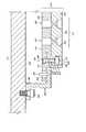
[0035]図2は、拡散プレート158の部分断面図である。拡散プレート158は、蓋アセンブリ110と面した第1または上流側部202と、この反対側に位置する、支持アセンブリ138と面した第2または上流側部204と含む。一実施形態では、拡散プレート158はアルミニウムから製造され、少なくとも下流側部204上に陽極処理が施されている。下流側部204上への陽極処理により、プラズマの均一性を増加させることが分かっている。後の処理中に放出されることで異物の原因となる、洗浄中のフッ素吸収を制限するために、場合により上流側部202には陽極処理を施さなくてもよい。 FIG. 2 is a partial cross-sectional view of the diffusing
[0036]一実施形態では、各々のガス通路162は、オリフィス穴214によって第2ボア212と結合した第1ボア210によって画成されており、この組み合わせがガス分配プレート158にかけて流路を形成する。第1ボア210は、ガス分配プレート158の上流側部202から底部218までの第1深さ230にかけて延びている。第1ボア210の底部218は、ガスが第1ボアからオリフィス穴210内に流入する際の流量制限を最小化するために、先細り、傾斜、面取りまたは丸くされている。一般的に、、第1ボア210の直径は約0.236〜0.553cm(約0.093〜0.218インチ)であり、一実施形態では約0.396cm(約0.156インチ)である。 [0036] In one embodiment, each
[0037]第2ボア212は拡散プレート158に形成され、下流側部204から約0.635〜0.918cm(約0.250〜約0.375インチ)の深さ232にかけて延びている。第2ボア212の直径は、一般的に、約0.474〜0.952cm(約0.187〜約0.375インチ)であり、約22〜35度の角度216でフレア型に広がっていてもよい。一実施形態では、第2ボア212の直径は0.812cm(0.320インチ)であり、約35度の角度216でフレア型に広がっている。別の実施形態では、近接した第2ボア212の縁282どうしの間の距離280は約25〜約85ミリメートルである。通常、第1ボア210の直径は第2ボア212の直径と少なくとも等しい、またはこれよりも小さいが、これに限定されるものではない。第2ボア212の底部220は、オリフィス穴214から出て第2ボア212内へ流入するガスの圧力損失を最小化するために、先細り、傾斜、面取り、または丸くされていてもよい。さらに、第2ボア212の露出面エリアを最小化するように機能する部分の下流側部204へのオリフィス穴214の付近と、基板に面した下流側部204との付近では、チャンバ洗浄中に供給されたフッ素に晒される拡散プレート158の下流エリアが減少し、これにより堆積した膜のフッ素異物の発生が減少する。 [0037] A
[0038]一般的に、オリフィス穴214は、第1穴210の底部218と第2ボア212の底部220を結合する。一般的に、オリフィス穴の直径は約0.25〜約0.74mm(約0.02〜約0.3インチ)であり、その長さ234は、典型的には約0.10〜約0.21cm(約0.040〜約0.085インチ)である。オリフィス穴214の長さ234と直径(またはこれ以外の形状的属性)は、ガス分配プレート158の上流側部202にかけてガスの分配を容易にするプレナム164内の背圧の主要なソースである。典型的に、オリフィス穴214は、複数のガス通路162の間に均一に構成されているが、しかし、オリフィス穴214通過の規制は、さらに多くのガスがガス分配プレート158の別のエリアに対する或る1つのエリアを通って流れるようにするために、ガス通路162の中でも異なる形状に構成することができる。例えば、ガラス基板の外辺部における堆積速度を加速化するように穿孔エリア116の縁にかけてより大量のガスが流れるようにするために、ガス分配プレート158の外辺部により接近したガス通路262内に設けられたオリフィス穴214は、より大きな直径および/またはより短い長さ234を有してもよい。 [0038] In general, the
[0039]オリフィス穴214の長さ234比較的短く、2つの大型直径ボア210、212の間に位置決めされているため、オリフィス穴214は、最小のドリル破損の可能性にて、ガス分配プレート158に効率的に製造することができる。そのため、本発明のガス分配プレート158は、穿孔エリアに形成した多数のガス通路のドリル破損と分配プレートからの引き抜きにかかる費用が共通して生じる従来のガス分配プレートと比較して、コスト安にて製造できる。さらに、蓋アセンブリ110を通って流入する洗浄剤に直接晒されるガス分配プレート158の上流側部202の表面エリアは、プレートの上流側部に直接形成したガス流オリフィスを有する従来のガス分配プレートよりも著しく小さく、陽極処理したガス分配プレート158のフッ素含有量は、複数の洗浄サイクルの期間にかけて減少する傾向にあり、これにより、処理中に放出されるフッ素の量が減少する。 [0039] Because the
[0040]オリフィス穴214に提供される全ての規制は、拡散プレート158の上流の存在する背圧に直接影響するため、洗浄中に使用される解離したフッ素の再組み合わせを防止するように構成する必要がある。これに関連し、オリフィス穴の直径は、穴の数に対比させなければならない。オリフィス穴の直径を大きくすることで、使用する穴の数を減らし、製造コストの削減を実現できるのに対し、隣接する第2ボア212の縁282同士の間隔を、約25〜約50ミリメートルのより低い範囲内で選択することで、より大量のガス流穴密度を有する従来の拡散プレートと比較した堆積均一性能を達成できる。 [0040] All restrictions provided to orifice
[0041]図2に示す実施形態では、ハンガープレート160と拡散プレート158は、撓み、歪みを生じることなく、または、ガス分配プレートアセンブリ118を通るガス流の均一性に影響する形で拡散プレート158に不利に応力をかけることなく、拡散プレート158の熱膨張と収縮を容易にする方法で結合することができる。一実施形態では、ハンガープレート160は、主本体262から外方へ延びた第1フランジ264と、第1フランジ264と反対方向に内方に延びた第2フランジ260とを含んだ多角形フレームである。あるいは、ハンガープレート160はフランジ付きシリンダであってもよい。第1フランジ264は複数の取り付け穴266を含んでおり、その各々は蓋アセンブリ110に形成されたねじ切りされた穴278と整列する。逃げ口を設けた固定具268の各々が取り付け穴266を貫通し、ねじ切りされた穴278内にねじ込まれて、ハンガープレート160を蓋アセンブリ110に固着させる。 [0041] In the embodiment shown in FIG. 2, the
[0042]第2フランジ260には、ドウェルピン244をそれぞれ保持する内部に形成された複数の穴270を含む。ドウェルピン244(図2中に1つ示す)は、第2フランジ260から第1フランジ262へ、そして蓋アセンブリ110の内面120へと上方に向かって延びている。拡散プレート158を貫通して形成された穴またはスロット246は、それぞれ対応するピン244を受容するよう適合されている。 [0042] The
[0043]さらに、図4に示すハンガープレート160の部分断面正面図を参照すると、拡散プレート158のスロット246は、拡散プレート158がドウェルピン244に対して移動できるよう、ドウェルピン244に対して十分大きいため、拡散プレート158とハンガープレート160と蓋アセンブリ110間の熱膨張の差の補正が容易になる。図4に示すように、典型的に、スロット246は、プレートアセンブリ118の2本の軸に沿った拡大を収容するために拡散プレート158の各側部に沿って、多角形方向に偏向されている。あるいは、スロット246を、円形のガス分配プレートに合わせて放射状に構成することもできる。これにより、分散プレートアセンブリ118が加熱および冷却された際に、拡散プレート158が蓋アセンブリ110に対して自由に移動することで、拡散プレート158がたわみ、またはこれ以外の、アセンブリ118を歪ませる、もしくは分配プレートアセンブリ118内を通るガスのパターン変形せる応力を含まないようになる。あるいは、拡散プレート158から延びているピンを受容するために、ハンガープレート160にスロットを形成してもよい。[0043] Further, referring to the partial cross-sectional front view of
[0044]図5は、ガス分配プレートアセンブリ500の別の実施形態を示す部分断面図である。ガス分配プレートアセンブリ500は、上述したものと類似する蓋アセンブリ110に取り付けられたハンガープレート160と拡散プレートアセンブリ502を含む。拡散プレートアセンブリ502は、拡散プレート506と結合した調整プレート504を含む。ガス分配プレートアセンブリ500と蓋アセンブリ110の間に画成されたプレナム510から処理チャンバの処理エリア512へガスを分配するために、調整プレート504と拡散プレート506にかけて複数のガス通路508が形成されている。 FIG. 5 is a partial cross-sectional view illustrating another embodiment of a gas
[0045]ガス通路508は、上述のガス通路162と類似して構成されているが、各ガス通路508の上流部分が調整プレート504にかけて形成され、下流部分が拡散プレート506にかけて形成されている点が異なる。例えば、第1ボア520の少なくとも一部分が調整プレート504に形成され、その一方で第2ボア522の少なくとも一部分が拡散プレート506に形成されている。第1ボア520と第2ボア522を流体結合するオリフィス穴524を、少なくとも部分的に、調整プレート504または拡散プレート506の少なくとも一方に形成できる。 [0045] The
[0046]図5に示した実施形態では、第1ボア520が調整プレート504にかけて、また一部分が拡散プレート506に形成されている。第2のボア522およびオリフィス穴524は、拡散プレートに形成される。ボアと穴520、522、524を別個のプレート504、506に製造することで、オリフィス穴524のドリルの長さと深さ(つまりプレート内の位置)が最小化されるに従ってより効率的な製造が可能になり、ドリル先端部破損の発生がさらに減少し、製造コストもさらに減少する。 In the embodiment shown in FIG. 5, a
[0047]ガス通路508の調整プレート504と拡散プレート506に形成された部分の嵌合および整列を確実に行うために、調整プレート504と拡散プレート506の間には複数の設置特徴部546が配置されている。一実施形態では、設置特徴部546は、調整プレート504と拡散プレート506の間に配置された複数の搭載ピン544(その内1本のみを図示)である。図5に示したこの実施形態では、設置ピン544が拡散プレート506から延び、調整プレート504を貫通した孔と圧着する嵌合ブッシング542と係合する。ピン544は、蓋アセンブリ110に対し調整プレート504及び拡散プレート506間の所定配向性とガス通路508の整列が確実に得られるように位置決めされる。調整プレート504と拡散プレート506は、固定具、リベット、ねじ、真鍮メッキ、溶接、接着、クランピング等のようなあらやる方法で互いに固定することができる。 [0047] A plurality of installation features 546 are disposed between the
[0048]図6は、調整プレート652と拡散プレート654を通って形成された複数のガス通路660を含む、拡散器分散プレートアセンブリ650の別の実施形態の部分断面図を示しており、ここで、調整プレート652は拡散プレート654に取り外し可能に固定されている。図6に示す実施形態では、調整プレート652と拡散プレート654は、破断性(Breakaway)固定具システム600(図6にはその内1つを図示)によって基準の間隔で結合している。ガス通路660は、上述したガス通路508に類似して構造されている。 [0048] FIG. 6 illustrates a partial cross-sectional view of another embodiment of a diffuser
[0049]破断性固定具システム600の各々は、固定具602と嵌合ナット604を含んでおり、典型的に、この両方はアルミニウムまたはその他適切な材料で製造されている。固定具材料による処理への影響を最小化するためにアルミニウム固定具の使用が有利である用途では、従来のアルミニウム固定具では加熱によって固くなってしまうために構成部品を取り外しと再度ねじ込みが必要であるところを、破断性固定具システム600を使用することで、調整プレート652と拡散器654が分離させることができる。これにより、ガス通路660の流れ特徴を変化させるように調整プレート652を変更することが可能であるため、アセンブリ全体を変更することなく、分配プレートアセンブリ650を所与の処理に適応させることができる。この特徴は、前述で組み入れたBloniganらにより2003年1月7日に出願された米国特許明細書第10/337,483号に詳細に論じられている。(事件番号第7651号)
[0050]一実施形態では、固定具602は頭部606、シャンク608、ねじ切りした部分610を有する。典型的に、頭部606は、調整プレート652の頂面614に形成したカウンタボア612内に配置される。穴616は、固定具602のシャンク608を受容するように、調整プレート652を貫通して、カウンタボア612と同心的に形成されている。シャンク608は、穴616と同心的に整列し拡散プレート654を貫通して形成された穴618を通過する。典型的に、シャンク608は、固定具602が所定量を超えたトルクに晒されると剪断を実行するネック部分620を含む。[0049] Each
[0050] In one embodiment, the
[0051]典型的に、ナット604は、調整プレート652と反対側に位置する拡散プレート654の下流側部624に形成したスロット622内に配置されている。スロット624は、拡散プレート654を貫通して形成した穴618と連通している。シャンク608は穴616、618を通過して、ねじ切り部分610をスロット622内に露出させる。スロット622内に配置されたナット602が固定具602のねじ切り部分610と嵌合する。スロット622は、プレート652、654を相互に対して接近させるように固定具602を緊締する際にナット604が回転してしまうことを防止するように構成される。さらに、拡散プレートアセンブリ650の2枚プレート式構成により、製造中にオリフィス穴694の形成に要する距離を実質的に減じて、製造中におけるドリル破損の発生をさらに低減することで、ガス通路660の経済的な製造がさらに容易になる。 [0051] Typically, the
[0052]このようにして、経済的な製造が可能なガス分配プレートアセンブリが得られた。さらに、こうして得たガス分配プレートアセンブリにより、プレートの幅にかけてオリフィス穴の形状を変更することで、および/または、アセンブリの1枚のプレートによって、ガスの流れ特徴を有利に調整することができる。 [0052] Thus, a gas distribution plate assembly was obtained that was economical to manufacture. Further, the gas distribution plate assembly thus obtained allows the gas flow characteristics to be advantageously adjusted by changing the shape of the orifice hole over the width of the plate and / or by a single plate of the assembly.
[0053]本発明の教示を採用したいくつかの好ましい実施形態を示し、詳細に記載したが、当業者は、これらの教示の採用を維持したこれ以外の多くの変更型の実施形態を案出することができる。 [0053] While several preferred embodiments employing the teachings of the present invention have been shown and described in detail, those skilled in the art have devised many other alternative embodiments that have maintained the adoption of these teachings. can do.
110…蓋アセンブリ110、116…穿孔エリア、118…ガス分配プレートアセンブリ、158…拡散プレート、160…ハンガープレート、162…ガス通路、164…プレナム、166…アパーチャ、202…上流側部、204…下流側部、244…ドウェルピン、246…スロット、264…第1フランジ、266…取り付け穴、268…固定具、282…縁。110:
Claims (26)
Translated fromJapanese上流側部と下流側部を有する拡散プレートと、
拡散プレートの上流側部と下流側部との間を通過する複数の同心ガス通路と、
を備え、
前記ガス通路の各々は、
円筒形状に形成され、前記上流側部から延び、第1直径を有する第1穴であって、その底部が先細り、傾斜、丸く形成、または面取りされている、前記第1穴と、
フレア型に形成され、前記下流側部から延び、第2直径を有する第2穴であって、その底部が先細り、傾斜、丸く形成、または面取りされている、前記第2穴と、
前記第2穴と前記第1穴の底部を流体結合し、前記第1穴と前記第2穴よりも小さい直径を有するオリフィスであって、少なくとも一つのオリフィス穴が、少なくとも一つの別のオリフィス穴とは異なる流量制限属性を有する、前記オリフィスと、
を含む、前記ガス分配プレートアセンブリ。A gas distribution plate assembly for a processing chamber, comprising:
A diffusion plate having an upstream side and a downstream side;
A plurality of concentric gas passages passing between the upstream side and the downstream side of the diffusion plate;
With
Each of the gas passages is
A first hole formed in a cylindrical shape, extending from the upstream side and having a first diameter, the bottom of which is tapered, inclined, rounded or chamfered;
A second hole formed in a flare shape, extending from the downstream side and having a second diameter, the bottom of which is tapered, inclined, rounded or chamfered;
An orifice that fluidly couples the second hole and the bottom of the first hole and has a smaller diameter than the first hole and the second hole, wherein at least one orifice hole is at least one other orifice hole. The orifice having a flow restriction attribute different from
Said gas distribution plate assembly.
前記ガス通路に形成された前記第1穴の少なくとも一部分を有する第1プレートと、
前記第1プレートと結合し、前記ガス通路に形成された前記第2穴の少なくとも一部分を有する第2プレートと、
を備える、請求項1に記載のガス分配プレートアセンブリ。The diffusion plate further comprises:
A first plate having at least a portion of the first hole formed in the gas passage;
A second plate coupled to the first plate and having at least a portion of the second hole formed in the gas passage;
The gas distribution plate assembly of claim 1, comprising:
アルミニウム上流側部と下流側部を有する拡散プレートアセンブリと、
前記拡散プレートアセンブリの前記上流側部と前記下流側部の間を通過する複数の同心ガス通路と、
を備え、
前記ガス通路の各々が、
前記上流側部から延び第1直径を有する第1穴と、
前記第1穴の底部と流体結合したオリフィス穴と、
前記オリフィス穴から下流側部へ延び第2直径を有するフレア型第2穴と、
を備え、前記オリフィス穴の直径が前記第1穴および前記第2穴よりも小さく、前記拡散プレートを貫通して形成された前記オリフィス穴の少なくとも一つが別のオリフィス穴の少なくとも1つとは異なる流量制限属性を有する、ガス分配プレートアセンブリ。A gas distribution plate assembly for a processing chamber, comprising:
A diffuser plate assembly having an aluminum upstream side and a downstream side;
A plurality of concentric gas passages passing between the upstream side and the downstream side of the diffusion plate assembly;
With
Each of the gas passages is
A first hole extending from the upstream side and having a first diameter;
An orifice hole fluidly coupled to the bottom of the first hole;
A flare-type second hole extending from the orifice hole to the downstream side and having a second diameter;
The orifice hole has a diameter smaller than that of the first hole and the second hole, and at least one of the orifice holes formed through the diffusion plate has a flow rate different from that of at least one of the other orifice holes. A gas distribution plate assembly having restricted attributes.
前記ガス通路に形成された前記第1穴の少なくとも一部分を有する第1プレートと、
前記第1プレートと結合し、前記ガス通路に形成された第2穴の少なくとも一部分を有する第2プレートと、
を備える、請求項10に記載のガス分配プレートアセンブリ。The diffusion plate assembly further comprises:
A first plate having at least a portion of the first hole formed in the gas passage;
A second plate coupled to the first plate and having at least a portion of a second hole formed in the gas passage;
The gas distribution plate assembly according to claim 10, comprising:
上流側部と下流側部を有する拡散プレートと、
前記拡散プレートを貫通して形成された複数の同心ガス通路であって、各ガス通路は:
円筒状に形成され、前記上流側部から延び、第1直径を有する第1穴と;
漏斗状に形成され、前記下流側部から延び、第2直径を有する第2穴と;
前記第1穴と前記第2穴を結合するオリフィス穴であって、前記オリフィス穴の少なくとも一つが、前記拡散プレートの中心における少なくとも一つのオリフィス穴の流量制限属性とは異なる流量制限属性を前記拡散プレートの周辺で有する、前記オリフィス穴と;
を備える、ガス分配プレートアセンブリ。A gas distribution plate assembly for a processing chamber, comprising:
A diffusion plate having an upstream side and a downstream side;
A plurality of concentric gas passages formed through the diffusion plate, each gas passage comprising:
A first hole formed in a cylindrical shape and extending from the upstream side and having a first diameter;
A second hole formed in a funnel shape, extending from the downstream side and having a second diameter;
Aorifice hole coupling the second hole and the first hole, at least one of theorifice holes,said diffusion different flow restriction attributes and flow restriction attributes of the at least oneorifice hole at the center of the diffuser plate Saidorifice hole having atthe periphery of theplate ;
A gas distribution plate assembly comprising:
ガス通路に形成された第1穴の少なくとも一部分を有する第1プレートと、
第1プレートと結合し、ガス通路に形成された第2穴の少なくとも一部分を有する第2プレートと、
を備える、請求項21に記載のガス分配プレートアセンブリ。The diffusion plate assembly
A first plate having at least a portion of a first hole formed in the gas passage;
A second plate coupled to the first plate and having at least a portion of a second hole formed in the gas passage;
The gas distribution plate assembly of claim 21, comprising:
Applications Claiming Priority (2)
| Application Number | Priority Date | Filing Date | Title |
|---|---|---|---|
| US10/417,592 | 2003-04-16 | ||
| US10/417,592US6942753B2 (en) | 2003-04-16 | 2003-04-16 | Gas distribution plate assembly for large area plasma enhanced chemical vapor deposition |
Related Parent Applications (1)
| Application Number | Title | Priority Date | Filing Date |
|---|---|---|---|
| JP2005518601ADivisionJP2006515039A (en) | 2003-04-16 | 2004-04-14 | Gas distribution plate assembly for large area plasma chemical vapor deposition |
Publications (2)
| Publication Number | Publication Date |
|---|---|
| JP2010077537A JP2010077537A (en) | 2010-04-08 |
| JP5302865B2true JP5302865B2 (en) | 2013-10-02 |
Family
ID=33158943
Family Applications (2)
| Application Number | Title | Priority Date | Filing Date |
|---|---|---|---|
| JP2005518601APendingJP2006515039A (en) | 2003-04-16 | 2004-04-14 | Gas distribution plate assembly for large area plasma chemical vapor deposition |
| JP2009272100AExpired - LifetimeJP5302865B2 (en) | 2003-04-16 | 2009-11-30 | Gas distribution plate assembly for large area plasma chemical vapor deposition |
Family Applications Before (1)
| Application Number | Title | Priority Date | Filing Date |
|---|---|---|---|
| JP2005518601APendingJP2006515039A (en) | 2003-04-16 | 2004-04-14 | Gas distribution plate assembly for large area plasma chemical vapor deposition |
Country Status (6)
| Country | Link |
|---|---|
| US (1) | US6942753B2 (en) |
| JP (2) | JP2006515039A (en) |
| KR (1) | KR100696021B1 (en) |
| CN (2) | CN1754008B (en) |
| TW (1) | TWI276701B (en) |
| WO (1) | WO2004094693A2 (en) |
Families Citing this family (630)
| Publication number | Priority date | Publication date | Assignee | Title |
|---|---|---|---|---|
| US6772827B2 (en)* | 2000-01-20 | 2004-08-10 | Applied Materials, Inc. | Suspended gas distribution manifold for plasma chamber |
| JP2005536042A (en)* | 2002-08-08 | 2005-11-24 | トリコン テクノロジーズ リミティド | Improved shower head |
| US7270713B2 (en)* | 2003-01-07 | 2007-09-18 | Applied Materials, Inc. | Tunable gas distribution plate assembly |
| US6942753B2 (en)* | 2003-04-16 | 2005-09-13 | Applied Materials, Inc. | Gas distribution plate assembly for large area plasma enhanced chemical vapor deposition |
| US8580076B2 (en)* | 2003-05-22 | 2013-11-12 | Lam Research Corporation | Plasma apparatus, gas distribution assembly for a plasma apparatus and processes therewith |
| US20050098106A1 (en)* | 2003-11-12 | 2005-05-12 | Tokyo Electron Limited | Method and apparatus for improved electrode plate |
| US20050103265A1 (en)* | 2003-11-19 | 2005-05-19 | Applied Materials, Inc., A Delaware Corporation | Gas distribution showerhead featuring exhaust apertures |
| JP4231417B2 (en)* | 2004-01-07 | 2009-02-25 | パナソニック株式会社 | Substrate processing apparatus and cleaning method thereof |
| JP4698251B2 (en)* | 2004-02-24 | 2011-06-08 | アプライド マテリアルズ インコーポレイテッド | Movable or flexible shower head mounting |
| US20050220568A1 (en)* | 2004-03-31 | 2005-10-06 | Tokyo Electron Limited | Method and system for fastening components used in plasma processing |
| US20050223986A1 (en)* | 2004-04-12 | 2005-10-13 | Choi Soo Y | Gas diffusion shower head design for large area plasma enhanced chemical vapor deposition |
| US8083853B2 (en) | 2004-05-12 | 2011-12-27 | Applied Materials, Inc. | Plasma uniformity control by gas diffuser hole design |
| US20050241767A1 (en)* | 2004-04-30 | 2005-11-03 | Ferris David S | Multi-piece baffle plate assembly for a plasma processing system |
| US8328939B2 (en)* | 2004-05-12 | 2012-12-11 | Applied Materials, Inc. | Diffuser plate with slit valve compensation |
| US8074599B2 (en)* | 2004-05-12 | 2011-12-13 | Applied Materials, Inc. | Plasma uniformity control by gas diffuser curvature |
| US20060011582A1 (en)* | 2004-07-14 | 2006-01-19 | Savas Stephen E | Fast isotropic etching system and process for large, non-circular substrates |
| KR20060014495A (en)* | 2004-08-11 | 2006-02-16 | 주식회사 유진테크 | Shower head of chemical vapor deposition system |
| US7429410B2 (en) | 2004-09-20 | 2008-09-30 | Applied Materials, Inc. | Diffuser gravity support |
| US20060090773A1 (en)* | 2004-11-04 | 2006-05-04 | Applied Materials, Inc. | Sulfur hexafluoride remote plasma source clean |
| US20060185590A1 (en)* | 2005-02-18 | 2006-08-24 | General Electric Company | High temperature chemical vapor deposition apparatus |
| US20060185591A1 (en)* | 2005-02-18 | 2006-08-24 | General Electric Company | High temperature chemical vapor deposition apparatus |
| DE602006011140D1 (en)* | 2005-04-05 | 2010-01-28 | Krosaki Harima Corp | GAS SHOW ERPLATE FOR A PLASMA PROCESSING DEVICE |
| JP4654738B2 (en)* | 2005-04-05 | 2011-03-23 | パナソニック株式会社 | Plasma processing equipment |
| KR100629358B1 (en)* | 2005-05-24 | 2006-10-02 | 삼성전자주식회사 | Shower head |
| US20060266288A1 (en)* | 2005-05-27 | 2006-11-30 | Applied Materials, Inc. | High plasma utilization for remote plasma clean |
| US8709162B2 (en)* | 2005-08-16 | 2014-04-29 | Applied Materials, Inc. | Active cooling substrate support |
| US20070044714A1 (en)* | 2005-08-31 | 2007-03-01 | Applied Materials, Inc. | Method and apparatus for maintaining a cross sectional shape of a diffuser during processing |
| US7641762B2 (en)* | 2005-09-02 | 2010-01-05 | Applied Materials, Inc. | Gas sealing skirt for suspended showerhead in process chamber |
| US20070084408A1 (en)* | 2005-10-13 | 2007-04-19 | Applied Materials, Inc. | Batch processing chamber with diffuser plate and injector assembly |
| US20070084406A1 (en)* | 2005-10-13 | 2007-04-19 | Joseph Yudovsky | Reaction chamber with opposing pockets for gas injection and exhaust |
| KR100752622B1 (en)* | 2006-02-17 | 2007-08-30 | 한양대학교 산학협력단 | Remote Plasma Generator |
| US20070254112A1 (en)* | 2006-04-26 | 2007-11-01 | Applied Materials, Inc. | Apparatus and method for high utilization of process chambers of a cluster system through staggered plasma cleaning |
| US8440049B2 (en)* | 2006-05-03 | 2013-05-14 | Applied Materials, Inc. | Apparatus for etching high aspect ratio features |
| US8475625B2 (en)* | 2006-05-03 | 2013-07-02 | Applied Materials, Inc. | Apparatus for etching high aspect ratio features |
| US7811085B2 (en)* | 2006-05-04 | 2010-10-12 | Honeywell International Inc. | Gas preheater for chemical vapor processing furnace |
| US7771194B2 (en)* | 2006-05-26 | 2010-08-10 | Honeywell International Inc. | Gas preheater for chemical vapor processing furnace having circuitous passages |
| US20070281106A1 (en)* | 2006-05-30 | 2007-12-06 | Applied Materials, Inc. | Process chamber for dielectric gapfill |
| US7776178B2 (en)* | 2006-10-25 | 2010-08-17 | Applied Materials, Inc. | Suspension for showerhead in process chamber |
| US8702866B2 (en) | 2006-12-18 | 2014-04-22 | Lam Research Corporation | Showerhead electrode assembly with gas flow modification for extended electrode life |
| JP4954734B2 (en)* | 2007-01-30 | 2012-06-20 | 東京エレクトロン株式会社 | Substrate processing apparatus and gas supply method |
| US7942969B2 (en)* | 2007-05-30 | 2011-05-17 | Applied Materials, Inc. | Substrate cleaning chamber and components |
| US20080317973A1 (en)* | 2007-06-22 | 2008-12-25 | White John M | Diffuser support |
| US8034410B2 (en) | 2007-07-17 | 2011-10-11 | Asm International N.V. | Protective inserts to line holes in parts for semiconductor process equipment |
| US7807222B2 (en)* | 2007-09-17 | 2010-10-05 | Asm International N.V. | Semiconductor processing parts having apertures with deposited coatings and methods for forming the same |
| US7976631B2 (en)* | 2007-10-16 | 2011-07-12 | Applied Materials, Inc. | Multi-gas straight channel showerhead |
| WO2009057583A1 (en)* | 2007-10-31 | 2009-05-07 | Tohoku University | Plasma processing system and plasma processing method |
| JP5150217B2 (en)* | 2007-11-08 | 2013-02-20 | 東京エレクトロン株式会社 | Shower plate and substrate processing apparatus |
| US20090120368A1 (en)* | 2007-11-08 | 2009-05-14 | Applied Materials, Inc. | Rotating temperature controlled substrate pedestal for film uniformity |
| US20090194021A1 (en)* | 2008-02-01 | 2009-08-06 | Scott Snodgrass | Dispenser for a coating apparatus having reduced sag |
| US8066895B2 (en)* | 2008-02-28 | 2011-11-29 | Applied Materials, Inc. | Method to control uniformity using tri-zone showerhead |
| WO2009133189A1 (en)* | 2008-05-02 | 2009-11-05 | Oerlikon Trading Ag, Truebbach | Plasma processing apparatus and method for the plasma processing of substrates |
| WO2009140440A1 (en) | 2008-05-13 | 2009-11-19 | Nanoink, Inc. | Dual-tip cantilever |
| JP5520455B2 (en)* | 2008-06-11 | 2014-06-11 | 東京エレクトロン株式会社 | Plasma processing equipment |
| US8221582B2 (en) | 2008-07-07 | 2012-07-17 | Lam Research Corporation | Clamped monolithic showerhead electrode |
| US8206506B2 (en) | 2008-07-07 | 2012-06-26 | Lam Research Corporation | Showerhead electrode |
| US8161906B2 (en) | 2008-07-07 | 2012-04-24 | Lam Research Corporation | Clamped showerhead electrode assembly |
| US9493875B2 (en)* | 2008-09-30 | 2016-11-15 | Eugene Technology Co., Ltd. | Shower head unit and chemical vapor deposition apparatus |
| US10378106B2 (en) | 2008-11-14 | 2019-08-13 | Asm Ip Holding B.V. | Method of forming insulation film by modified PEALD |
| DE102008044024A1 (en)* | 2008-11-24 | 2010-05-27 | Robert Bosch Gmbh | Coating method and coating device |
| US9714465B2 (en)* | 2008-12-01 | 2017-07-25 | Applied Materials, Inc. | Gas distribution blocker apparatus |
| US9394608B2 (en) | 2009-04-06 | 2016-07-19 | Asm America, Inc. | Semiconductor processing reactor and components thereof |
| US8402918B2 (en) | 2009-04-07 | 2013-03-26 | Lam Research Corporation | Showerhead electrode with centering feature |
| US8272346B2 (en) | 2009-04-10 | 2012-09-25 | Lam Research Corporation | Gasket with positioning feature for clamped monolithic showerhead electrode |
| US8147614B2 (en)* | 2009-06-09 | 2012-04-03 | Applied Materials, Inc. | Multi-gas flow diffuser |
| JP5777615B2 (en) | 2009-07-15 | 2015-09-09 | アプライド マテリアルズ インコーポレイテッドApplied Materials,Incorporated | Flow control mechanism of CVD chamber |
| US8657959B2 (en)* | 2009-07-31 | 2014-02-25 | E I Du Pont De Nemours And Company | Apparatus for atomic layer deposition on a moving substrate |
| US8802201B2 (en) | 2009-08-14 | 2014-08-12 | Asm America, Inc. | Systems and methods for thin-film deposition of metal oxides using excited nitrogen-oxygen species |
| SG169960A1 (en)* | 2009-09-18 | 2011-04-29 | Lam Res Corp | Clamped monolithic showerhead electrode |
| WO2011044451A2 (en)* | 2009-10-09 | 2011-04-14 | Applied Materials, Inc. | Multi-gas centrally cooled showerhead design |
| JP3160877U (en)* | 2009-10-13 | 2010-07-15 | ラム リサーチ コーポレーションLam Research Corporation | End-clamping and machine-fixed inner electrode of showerhead electrode assembly |
| TWI394986B (en)* | 2009-11-09 | 2013-05-01 | Global Material Science Co Ltd | Diffuser structure and manufacturing method thereof |
| CN102064082B (en)* | 2009-11-13 | 2014-11-05 | 世界中心科技股份有限公司 | Diffusion plate structure and manufacturing method thereof |
| JP5835722B2 (en)* | 2009-12-10 | 2015-12-24 | オルボテック エルティ ソラー,エルエルシー | Automatic ranking multi-directional serial processor |
| EP2360292B1 (en)* | 2010-02-08 | 2012-03-28 | Roth & Rau AG | Parallel plate reactor for uniform thin film deposition with reduced tool foot-print |
| US20110198034A1 (en)* | 2010-02-11 | 2011-08-18 | Jennifer Sun | Gas distribution showerhead with coating material for semiconductor processing |
| JP6104157B2 (en)* | 2010-05-21 | 2017-03-29 | アプライド マテリアルズ インコーポレイテッドApplied Materials,Incorporated | Ceramic insulator fitted snugly to a large area electrode |
| US9324576B2 (en) | 2010-05-27 | 2016-04-26 | Applied Materials, Inc. | Selective etch for silicon films |
| US8721791B2 (en) | 2010-07-28 | 2014-05-13 | Applied Materials, Inc. | Showerhead support structure for improved gas flow |
| US8573152B2 (en) | 2010-09-03 | 2013-11-05 | Lam Research Corporation | Showerhead electrode |
| US8741778B2 (en) | 2010-12-14 | 2014-06-03 | Applied Materials, Inc. | Uniform dry etch in two stages |
| US10283321B2 (en) | 2011-01-18 | 2019-05-07 | Applied Materials, Inc. | Semiconductor processing system and methods using capacitively coupled plasma |
| US20120180954A1 (en) | 2011-01-18 | 2012-07-19 | Applied Materials, Inc. | Semiconductor processing system and methods using capacitively coupled plasma |
| US8771539B2 (en) | 2011-02-22 | 2014-07-08 | Applied Materials, Inc. | Remotely-excited fluorine and water vapor etch |
| US9064815B2 (en) | 2011-03-14 | 2015-06-23 | Applied Materials, Inc. | Methods for etch of metal and metal-oxide films |
| US8999856B2 (en) | 2011-03-14 | 2015-04-07 | Applied Materials, Inc. | Methods for etch of sin films |
| US9129778B2 (en) | 2011-03-18 | 2015-09-08 | Lam Research Corporation | Fluid distribution members and/or assemblies |
| US9312155B2 (en) | 2011-06-06 | 2016-04-12 | Asm Japan K.K. | High-throughput semiconductor-processing apparatus equipped with multiple dual-chamber modules |
| US10364496B2 (en) | 2011-06-27 | 2019-07-30 | Asm Ip Holding B.V. | Dual section module having shared and unshared mass flow controllers |
| US10854498B2 (en) | 2011-07-15 | 2020-12-01 | Asm Ip Holding B.V. | Wafer-supporting device and method for producing same |
| US20130023129A1 (en) | 2011-07-20 | 2013-01-24 | Asm America, Inc. | Pressure transmitter for a semiconductor processing environment |
| US8771536B2 (en) | 2011-08-01 | 2014-07-08 | Applied Materials, Inc. | Dry-etch for silicon-and-carbon-containing films |
| US8679982B2 (en) | 2011-08-26 | 2014-03-25 | Applied Materials, Inc. | Selective suppression of dry-etch rate of materials containing both silicon and oxygen |
| US8679983B2 (en) | 2011-09-01 | 2014-03-25 | Applied Materials, Inc. | Selective suppression of dry-etch rate of materials containing both silicon and nitrogen |
| US8927390B2 (en) | 2011-09-26 | 2015-01-06 | Applied Materials, Inc. | Intrench profile |
| US8808563B2 (en) | 2011-10-07 | 2014-08-19 | Applied Materials, Inc. | Selective etch of silicon by way of metastable hydrogen termination |
| US9109754B2 (en)* | 2011-10-19 | 2015-08-18 | Applied Materials, Inc. | Apparatus and method for providing uniform flow of gas |
| US9017481B1 (en) | 2011-10-28 | 2015-04-28 | Asm America, Inc. | Process feed management for semiconductor substrate processing |
| WO2013070436A1 (en) | 2011-11-08 | 2013-05-16 | Applied Materials, Inc. | Methods of reducing substrate dislocation during gapfill processing |
| WO2013070438A1 (en)* | 2011-11-08 | 2013-05-16 | Applied Materials, Inc. | Precursor distribution features for improved deposition uniformity |
| KR101361711B1 (en)* | 2011-12-30 | 2014-02-12 | 엘아이지에이디피 주식회사 | Supporting unit for supporting a processing chamber and apparatus for processing a substrate including the same |
| US20130273239A1 (en) | 2012-03-13 | 2013-10-17 | Universal Display Corporation | Nozzle design for organic vapor jet printing |
| KR101441478B1 (en) | 2012-07-09 | 2014-09-17 | 주식회사 에스에프에이 | Chemical Vapor Deposition Apparatus for Flat Display |
| US9267739B2 (en) | 2012-07-18 | 2016-02-23 | Applied Materials, Inc. | Pedestal with multi-zone temperature control and multiple purge capabilities |
| US9373517B2 (en) | 2012-08-02 | 2016-06-21 | Applied Materials, Inc. | Semiconductor processing with DC assisted RF power for improved control |
| US9659799B2 (en) | 2012-08-28 | 2017-05-23 | Asm Ip Holding B.V. | Systems and methods for dynamic semiconductor process scheduling |
| US8889566B2 (en) | 2012-09-11 | 2014-11-18 | Applied Materials, Inc. | Low cost flowable dielectric films |
| US9021985B2 (en) | 2012-09-12 | 2015-05-05 | Asm Ip Holdings B.V. | Process gas management for an inductively-coupled plasma deposition reactor |
| US9034770B2 (en) | 2012-09-17 | 2015-05-19 | Applied Materials, Inc. | Differential silicon oxide etch |
| US9023734B2 (en) | 2012-09-18 | 2015-05-05 | Applied Materials, Inc. | Radical-component oxide etch |
| US9390937B2 (en) | 2012-09-20 | 2016-07-12 | Applied Materials, Inc. | Silicon-carbon-nitride selective etch |
| US9132436B2 (en) | 2012-09-21 | 2015-09-15 | Applied Materials, Inc. | Chemical control features in wafer process equipment |
| US10714315B2 (en) | 2012-10-12 | 2020-07-14 | Asm Ip Holdings B.V. | Semiconductor reaction chamber showerhead |
| US8765574B2 (en) | 2012-11-09 | 2014-07-01 | Applied Materials, Inc. | Dry etch process |
| US8969212B2 (en) | 2012-11-20 | 2015-03-03 | Applied Materials, Inc. | Dry-etch selectivity |
| US8980763B2 (en) | 2012-11-30 | 2015-03-17 | Applied Materials, Inc. | Dry-etch for selective tungsten removal |
| US9064816B2 (en) | 2012-11-30 | 2015-06-23 | Applied Materials, Inc. | Dry-etch for selective oxidation removal |
| US9111877B2 (en) | 2012-12-18 | 2015-08-18 | Applied Materials, Inc. | Non-local plasma oxide etch |
| US8921234B2 (en) | 2012-12-21 | 2014-12-30 | Applied Materials, Inc. | Selective titanium nitride etching |
| KR101488878B1 (en)* | 2012-12-28 | 2015-02-04 | 주식회사 에스에프에이 | Gas distribution assembly |
| US9018108B2 (en) | 2013-01-25 | 2015-04-28 | Applied Materials, Inc. | Low shrinkage dielectric films |
| US20160376700A1 (en) | 2013-02-01 | 2016-12-29 | Asm Ip Holding B.V. | System for treatment of deposition reactor |
| US10256079B2 (en) | 2013-02-08 | 2019-04-09 | Applied Materials, Inc. | Semiconductor processing systems having multiple plasma configurations |
| US9362130B2 (en) | 2013-03-01 | 2016-06-07 | Applied Materials, Inc. | Enhanced etching processes using remote plasma sources |
| US9040422B2 (en) | 2013-03-05 | 2015-05-26 | Applied Materials, Inc. | Selective titanium nitride removal |
| US8801952B1 (en) | 2013-03-07 | 2014-08-12 | Applied Materials, Inc. | Conformal oxide dry etch |
| US9484191B2 (en) | 2013-03-08 | 2016-11-01 | Asm Ip Holding B.V. | Pulsed remote plasma method and system |
| US9589770B2 (en) | 2013-03-08 | 2017-03-07 | Asm Ip Holding B.V. | Method and systems for in-situ formation of intermediate reactive species |
| US10170282B2 (en) | 2013-03-08 | 2019-01-01 | Applied Materials, Inc. | Insulated semiconductor faceplate designs |
| US10403521B2 (en)* | 2013-03-13 | 2019-09-03 | Applied Materials, Inc. | Modular substrate heater for efficient thermal cycling |
| US20140271097A1 (en) | 2013-03-15 | 2014-09-18 | Applied Materials, Inc. | Processing systems and methods for halide scavenging |
| CN104099583B (en)* | 2013-04-09 | 2016-06-08 | 北京北方微电子基地设备工艺研究中心有限责任公司 | A kind of air intake installation, reaction chamber and plasma processing device |
| US8895449B1 (en) | 2013-05-16 | 2014-11-25 | Applied Materials, Inc. | Delicate dry clean |
| US9114438B2 (en) | 2013-05-21 | 2015-08-25 | Applied Materials, Inc. | Copper residue chamber clean |
| US20150011025A1 (en)* | 2013-07-03 | 2015-01-08 | Tsmc Solar Ltd. | Enhanced selenium supply in copper indium gallium selenide processes |
| US9493879B2 (en) | 2013-07-12 | 2016-11-15 | Applied Materials, Inc. | Selective sputtering for pattern transfer |
| US9773648B2 (en) | 2013-08-30 | 2017-09-26 | Applied Materials, Inc. | Dual discharge modes operation for remote plasma |
| US8956980B1 (en) | 2013-09-16 | 2015-02-17 | Applied Materials, Inc. | Selective etch of silicon nitride |
| US9240412B2 (en) | 2013-09-27 | 2016-01-19 | Asm Ip Holding B.V. | Semiconductor structure and device and methods of forming same using selective epitaxial process |
| TW201517112A (en)* | 2013-10-09 | 2015-05-01 | Applied Materials Inc | Multizone hollow cathode discharge system with coaxial and azimuthal symmetry and with consistent central trigger |
| US20150111394A1 (en)* | 2013-10-23 | 2015-04-23 | Taiwan Semiconductor Manufacturing Co., Ltd. | Mechanisms for forming uniform film on semiconductor substrate |
| US8951429B1 (en) | 2013-10-29 | 2015-02-10 | Applied Materials, Inc. | Tungsten oxide processing |
| US9576809B2 (en) | 2013-11-04 | 2017-02-21 | Applied Materials, Inc. | Etch suppression with germanium |
| US9236265B2 (en) | 2013-11-04 | 2016-01-12 | Applied Materials, Inc. | Silicon germanium processing |
| US9520303B2 (en) | 2013-11-12 | 2016-12-13 | Applied Materials, Inc. | Aluminum selective etch |
| US9245762B2 (en) | 2013-12-02 | 2016-01-26 | Applied Materials, Inc. | Procedure for etch rate consistency |
| US9117855B2 (en) | 2013-12-04 | 2015-08-25 | Applied Materials, Inc. | Polarity control for remote plasma |
| US9287095B2 (en) | 2013-12-17 | 2016-03-15 | Applied Materials, Inc. | Semiconductor system assemblies and methods of operation |
| US9263278B2 (en) | 2013-12-17 | 2016-02-16 | Applied Materials, Inc. | Dopant etch selectivity control |
| US9190293B2 (en) | 2013-12-18 | 2015-11-17 | Applied Materials, Inc. | Even tungsten etch for high aspect ratio trenches |
| US9287134B2 (en) | 2014-01-17 | 2016-03-15 | Applied Materials, Inc. | Titanium oxide etch |
| US9484190B2 (en)* | 2014-01-25 | 2016-11-01 | Yuri Glukhoy | Showerhead-cooler system of a semiconductor-processing chamber for semiconductor wafers of large area |
| US9293568B2 (en) | 2014-01-27 | 2016-03-22 | Applied Materials, Inc. | Method of fin patterning |
| US9396989B2 (en) | 2014-01-27 | 2016-07-19 | Applied Materials, Inc. | Air gaps between copper lines |
| WO2015116245A1 (en)* | 2014-01-30 | 2015-08-06 | Applied Materials, Inc. | Gas confiner assembly for eliminating shadow frame |
| US9385028B2 (en) | 2014-02-03 | 2016-07-05 | Applied Materials, Inc. | Air gap process |
| US10683571B2 (en) | 2014-02-25 | 2020-06-16 | Asm Ip Holding B.V. | Gas supply manifold and method of supplying gases to chamber using same |
| US9499898B2 (en) | 2014-03-03 | 2016-11-22 | Applied Materials, Inc. | Layered thin film heater and method of fabrication |
| US9299575B2 (en) | 2014-03-17 | 2016-03-29 | Applied Materials, Inc. | Gas-phase tungsten etch |
| US10167557B2 (en) | 2014-03-18 | 2019-01-01 | Asm Ip Holding B.V. | Gas distribution system, reactor including the system, and methods of using the same |
| US11015245B2 (en) | 2014-03-19 | 2021-05-25 | Asm Ip Holding B.V. | Gas-phase reactor and system having exhaust plenum and components thereof |
| US9299537B2 (en) | 2014-03-20 | 2016-03-29 | Applied Materials, Inc. | Radial waveguide systems and methods for post-match control of microwaves |
| US9299538B2 (en) | 2014-03-20 | 2016-03-29 | Applied Materials, Inc. | Radial waveguide systems and methods for post-match control of microwaves |
| US9136273B1 (en) | 2014-03-21 | 2015-09-15 | Applied Materials, Inc. | Flash gate air gap |
| CN104952760A (en)* | 2014-03-24 | 2015-09-30 | 北京北方微电子基地设备工艺研究中心有限责任公司 | Intake device and semiconductor processing equipment |
| US9903020B2 (en) | 2014-03-31 | 2018-02-27 | Applied Materials, Inc. | Generation of compact alumina passivation layers on aluminum plasma equipment components |
| US9269590B2 (en) | 2014-04-07 | 2016-02-23 | Applied Materials, Inc. | Spacer formation |
| US9309598B2 (en) | 2014-05-28 | 2016-04-12 | Applied Materials, Inc. | Oxide and metal removal |
| US9847289B2 (en) | 2014-05-30 | 2017-12-19 | Applied Materials, Inc. | Protective via cap for improved interconnect performance |
| US9406523B2 (en) | 2014-06-19 | 2016-08-02 | Applied Materials, Inc. | Highly selective doped oxide removal method |
| US9378969B2 (en) | 2014-06-19 | 2016-06-28 | Applied Materials, Inc. | Low temperature gas-phase carbon removal |
| US9412581B2 (en) | 2014-07-16 | 2016-08-09 | Applied Materials, Inc. | Low-K dielectric gapfill by flowable deposition |
| US9425058B2 (en) | 2014-07-24 | 2016-08-23 | Applied Materials, Inc. | Simplified litho-etch-litho-etch process |
| US10858737B2 (en)* | 2014-07-28 | 2020-12-08 | Asm Ip Holding B.V. | Showerhead assembly and components thereof |
| US9378978B2 (en) | 2014-07-31 | 2016-06-28 | Applied Materials, Inc. | Integrated oxide recess and floating gate fin trimming |
| US9159606B1 (en) | 2014-07-31 | 2015-10-13 | Applied Materials, Inc. | Metal air gap |
| US9496167B2 (en) | 2014-07-31 | 2016-11-15 | Applied Materials, Inc. | Integrated bit-line airgap formation and gate stack post clean |
| US9165786B1 (en) | 2014-08-05 | 2015-10-20 | Applied Materials, Inc. | Integrated oxide and nitride recess for better channel contact in 3D architectures |
| US9659753B2 (en) | 2014-08-07 | 2017-05-23 | Applied Materials, Inc. | Grooved insulator to reduce leakage current |
| US9553102B2 (en) | 2014-08-19 | 2017-01-24 | Applied Materials, Inc. | Tungsten separation |
| US9890456B2 (en) | 2014-08-21 | 2018-02-13 | Asm Ip Holding B.V. | Method and system for in situ formation of gas-phase compounds |
| US9355856B2 (en) | 2014-09-12 | 2016-05-31 | Applied Materials, Inc. | V trench dry etch |
| US9355862B2 (en) | 2014-09-24 | 2016-05-31 | Applied Materials, Inc. | Fluorine-based hardmask removal |
| US9368364B2 (en) | 2014-09-24 | 2016-06-14 | Applied Materials, Inc. | Silicon etch process with tunable selectivity to SiO2 and other materials |
| US9613822B2 (en) | 2014-09-25 | 2017-04-04 | Applied Materials, Inc. | Oxide etch selectivity enhancement |
| US10941490B2 (en) | 2014-10-07 | 2021-03-09 | Asm Ip Holding B.V. | Multiple temperature range susceptor, assembly, reactor and system including the susceptor, and methods of using the same |
| US9657845B2 (en) | 2014-10-07 | 2017-05-23 | Asm Ip Holding B.V. | Variable conductance gas distribution apparatus and method |
| US9355922B2 (en) | 2014-10-14 | 2016-05-31 | Applied Materials, Inc. | Systems and methods for internal surface conditioning in plasma processing equipment |
| US9966240B2 (en) | 2014-10-14 | 2018-05-08 | Applied Materials, Inc. | Systems and methods for internal surface conditioning assessment in plasma processing equipment |
| KR102300403B1 (en) | 2014-11-19 | 2021-09-09 | 에이에스엠 아이피 홀딩 비.브이. | Method of depositing thin film |
| DE102015110440A1 (en)* | 2014-11-20 | 2016-05-25 | Aixtron Se | CVD or PVD reactor for coating large-area substrates |
| US11637002B2 (en) | 2014-11-26 | 2023-04-25 | Applied Materials, Inc. | Methods and systems to enhance process uniformity |
| US9299583B1 (en) | 2014-12-05 | 2016-03-29 | Applied Materials, Inc. | Aluminum oxide selective etch |
| US10573496B2 (en) | 2014-12-09 | 2020-02-25 | Applied Materials, Inc. | Direct outlet toroidal plasma source |
| US10224210B2 (en) | 2014-12-09 | 2019-03-05 | Applied Materials, Inc. | Plasma processing system with direct outlet toroidal plasma source |
| KR102263121B1 (en) | 2014-12-22 | 2021-06-09 | 에이에스엠 아이피 홀딩 비.브이. | Semiconductor device and manufacuring method thereof |
| US9502258B2 (en) | 2014-12-23 | 2016-11-22 | Applied Materials, Inc. | Anisotropic gap etch |
| US9343272B1 (en) | 2015-01-08 | 2016-05-17 | Applied Materials, Inc. | Self-aligned process |
| US11257693B2 (en) | 2015-01-09 | 2022-02-22 | Applied Materials, Inc. | Methods and systems to improve pedestal temperature control |
| US9373522B1 (en) | 2015-01-22 | 2016-06-21 | Applied Mateials, Inc. | Titanium nitride removal |
| US9449846B2 (en) | 2015-01-28 | 2016-09-20 | Applied Materials, Inc. | Vertical gate separation |
| US20160225652A1 (en) | 2015-02-03 | 2016-08-04 | Applied Materials, Inc. | Low temperature chuck for plasma processing systems |
| US9728437B2 (en) | 2015-02-03 | 2017-08-08 | Applied Materials, Inc. | High temperature chuck for plasma processing systems |
| US9881805B2 (en) | 2015-03-02 | 2018-01-30 | Applied Materials, Inc. | Silicon selective removal |
| US10529542B2 (en) | 2015-03-11 | 2020-01-07 | Asm Ip Holdings B.V. | Cross-flow reactor and method |
| US10276355B2 (en) | 2015-03-12 | 2019-04-30 | Asm Ip Holding B.V. | Multi-zone reactor, system including the reactor, and method of using the same |
| US11384432B2 (en)* | 2015-04-22 | 2022-07-12 | Applied Materials, Inc. | Atomic layer deposition chamber with funnel-shaped gas dispersion channel and gas distribution plate |
| US12281385B2 (en)* | 2015-06-15 | 2025-04-22 | Taiwan Semiconductor Manufacturing Co., Ltd. | Gas dispenser and deposition apparatus using the same |
| US10458018B2 (en) | 2015-06-26 | 2019-10-29 | Asm Ip Holding B.V. | Structures including metal carbide material, devices including the structures, and methods of forming same |
| US10600673B2 (en) | 2015-07-07 | 2020-03-24 | Asm Ip Holding B.V. | Magnetic susceptor to baseplate seal |
| US10043661B2 (en) | 2015-07-13 | 2018-08-07 | Asm Ip Holding B.V. | Method for protecting layer by forming hydrocarbon-based extremely thin film |
| US10083836B2 (en) | 2015-07-24 | 2018-09-25 | Asm Ip Holding B.V. | Formation of boron-doped titanium metal films with high work function |
| US9691645B2 (en) | 2015-08-06 | 2017-06-27 | Applied Materials, Inc. | Bolted wafer chuck thermal management systems and methods for wafer processing systems |
| US9741593B2 (en) | 2015-08-06 | 2017-08-22 | Applied Materials, Inc. | Thermal management systems and methods for wafer processing systems |
| US9349605B1 (en) | 2015-08-07 | 2016-05-24 | Applied Materials, Inc. | Oxide etch selectivity systems and methods |
| US10504700B2 (en) | 2015-08-27 | 2019-12-10 | Applied Materials, Inc. | Plasma etching systems and methods with secondary plasma injection |
| US9960072B2 (en) | 2015-09-29 | 2018-05-01 | Asm Ip Holding B.V. | Variable adjustment for precise matching of multiple chamber cavity housings |
| JP6426298B2 (en)* | 2015-10-19 | 2018-11-21 | 東芝三菱電機産業システム株式会社 | Film deposition system |
| US10211308B2 (en) | 2015-10-21 | 2019-02-19 | Asm Ip Holding B.V. | NbMC layers |
| US10322384B2 (en) | 2015-11-09 | 2019-06-18 | Asm Ip Holding B.V. | Counter flow mixer for process chamber |
| TWI733712B (en)* | 2015-12-18 | 2021-07-21 | 美商應用材料股份有限公司 | A diffuser for a deposition chamber and an electrode for a deposition chamber |
| US11139308B2 (en) | 2015-12-29 | 2021-10-05 | Asm Ip Holding B.V. | Atomic layer deposition of III-V compounds to form V-NAND devices |
| US10468251B2 (en) | 2016-02-19 | 2019-11-05 | Asm Ip Holding B.V. | Method for forming spacers using silicon nitride film for spacer-defined multiple patterning |
| US10529554B2 (en) | 2016-02-19 | 2020-01-07 | Asm Ip Holding B.V. | Method for forming silicon nitride film selectively on sidewalls or flat surfaces of trenches |
| US10501866B2 (en) | 2016-03-09 | 2019-12-10 | Asm Ip Holding B.V. | Gas distribution apparatus for improved film uniformity in an epitaxial system |
| US10343920B2 (en) | 2016-03-18 | 2019-07-09 | Asm Ip Holding B.V. | Aligned carbon nanotubes |
| US9892913B2 (en) | 2016-03-24 | 2018-02-13 | Asm Ip Holding B.V. | Radial and thickness control via biased multi-port injection settings |
| US10190213B2 (en) | 2016-04-21 | 2019-01-29 | Asm Ip Holding B.V. | Deposition of metal borides |
| US10087522B2 (en) | 2016-04-21 | 2018-10-02 | Asm Ip Holding B.V. | Deposition of metal borides |
| US10865475B2 (en) | 2016-04-21 | 2020-12-15 | Asm Ip Holding B.V. | Deposition of metal borides and silicides |
| US10367080B2 (en) | 2016-05-02 | 2019-07-30 | Asm Ip Holding B.V. | Method of forming a germanium oxynitride film |
| US10032628B2 (en) | 2016-05-02 | 2018-07-24 | Asm Ip Holding B.V. | Source/drain performance through conformal solid state doping |
| KR102592471B1 (en) | 2016-05-17 | 2023-10-20 | 에이에스엠 아이피 홀딩 비.브이. | Method of forming metal interconnection and method of fabricating semiconductor device using the same |
| US10504754B2 (en) | 2016-05-19 | 2019-12-10 | Applied Materials, Inc. | Systems and methods for improved semiconductor etching and component protection |
| US10522371B2 (en) | 2016-05-19 | 2019-12-31 | Applied Materials, Inc. | Systems and methods for improved semiconductor etching and component protection |
| US11453943B2 (en) | 2016-05-25 | 2022-09-27 | Asm Ip Holding B.V. | Method for forming carbon-containing silicon/metal oxide or nitride film by ALD using silicon precursor and hydrocarbon precursor |
| KR102589743B1 (en)* | 2016-06-10 | 2023-10-17 | 주식회사 뉴파워 프라즈마 | Plasma chamber having gas distribution plate for uniform gas distribution |
| US10388509B2 (en) | 2016-06-28 | 2019-08-20 | Asm Ip Holding B.V. | Formation of epitaxial layers via dislocation filtering |
| US9865484B1 (en) | 2016-06-29 | 2018-01-09 | Applied Materials, Inc. | Selective etch using material modification and RF pulsing |
| US10612137B2 (en) | 2016-07-08 | 2020-04-07 | Asm Ip Holdings B.V. | Organic reactants for atomic layer deposition |
| US9859151B1 (en) | 2016-07-08 | 2018-01-02 | Asm Ip Holding B.V. | Selective film deposition method to form air gaps |
| US9793135B1 (en) | 2016-07-14 | 2017-10-17 | ASM IP Holding B.V | Method of cyclic dry etching using etchant film |
| US10714385B2 (en) | 2016-07-19 | 2020-07-14 | Asm Ip Holding B.V. | Selective deposition of tungsten |
| KR102354490B1 (en) | 2016-07-27 | 2022-01-21 | 에이에스엠 아이피 홀딩 비.브이. | Method of processing a substrate |
| US9887082B1 (en) | 2016-07-28 | 2018-02-06 | Asm Ip Holding B.V. | Method and apparatus for filling a gap |
| KR102532607B1 (en) | 2016-07-28 | 2023-05-15 | 에이에스엠 아이피 홀딩 비.브이. | Substrate processing apparatus and method of operating the same |
| US9812320B1 (en) | 2016-07-28 | 2017-11-07 | Asm Ip Holding B.V. | Method and apparatus for filling a gap |
| US10177025B2 (en) | 2016-07-28 | 2019-01-08 | Asm Ip Holding B.V. | Method and apparatus for filling a gap |
| US10395919B2 (en) | 2016-07-28 | 2019-08-27 | Asm Ip Holding B.V. | Method and apparatus for filling a gap |
| US10090316B2 (en) | 2016-09-01 | 2018-10-02 | Asm Ip Holding B.V. | 3D stacked multilayer semiconductor memory using doped select transistor channel |
| US10062575B2 (en) | 2016-09-09 | 2018-08-28 | Applied Materials, Inc. | Poly directional etch by oxidation |
| US10629473B2 (en) | 2016-09-09 | 2020-04-21 | Applied Materials, Inc. | Footing removal for nitride spacer |
| US10546729B2 (en) | 2016-10-04 | 2020-01-28 | Applied Materials, Inc. | Dual-channel showerhead with improved profile |
| US9721789B1 (en) | 2016-10-04 | 2017-08-01 | Applied Materials, Inc. | Saving ion-damaged spacers |
| US9934942B1 (en) | 2016-10-04 | 2018-04-03 | Applied Materials, Inc. | Chamber with flow-through source |
| US10062585B2 (en) | 2016-10-04 | 2018-08-28 | Applied Materials, Inc. | Oxygen compatible plasma source |
| US10062579B2 (en) | 2016-10-07 | 2018-08-28 | Applied Materials, Inc. | Selective SiN lateral recess |
| US9947549B1 (en) | 2016-10-10 | 2018-04-17 | Applied Materials, Inc. | Cobalt-containing material removal |
| US10410943B2 (en) | 2016-10-13 | 2019-09-10 | Asm Ip Holding B.V. | Method for passivating a surface of a semiconductor and related systems |
| US10643826B2 (en) | 2016-10-26 | 2020-05-05 | Asm Ip Holdings B.V. | Methods for thermally calibrating reaction chambers |
| US11532757B2 (en) | 2016-10-27 | 2022-12-20 | Asm Ip Holding B.V. | Deposition of charge trapping layers |
| US10643904B2 (en) | 2016-11-01 | 2020-05-05 | Asm Ip Holdings B.V. | Methods for forming a semiconductor device and related semiconductor device structures |
| US10714350B2 (en) | 2016-11-01 | 2020-07-14 | ASM IP Holdings, B.V. | Methods for forming a transition metal niobium nitride film on a substrate by atomic layer deposition and related semiconductor device structures |
| US10229833B2 (en) | 2016-11-01 | 2019-03-12 | Asm Ip Holding B.V. | Methods for forming a transition metal nitride film on a substrate by atomic layer deposition and related semiconductor device structures |
| US10435790B2 (en) | 2016-11-01 | 2019-10-08 | Asm Ip Holding B.V. | Method of subatmospheric plasma-enhanced ALD using capacitively coupled electrodes with narrow gap |
| US10134757B2 (en) | 2016-11-07 | 2018-11-20 | Asm Ip Holding B.V. | Method of processing a substrate and a device manufactured by using the method |
| US10163696B2 (en) | 2016-11-11 | 2018-12-25 | Applied Materials, Inc. | Selective cobalt removal for bottom up gapfill |
| US9768034B1 (en) | 2016-11-11 | 2017-09-19 | Applied Materials, Inc. | Removal methods for high aspect ratio structures |
| US10026621B2 (en) | 2016-11-14 | 2018-07-17 | Applied Materials, Inc. | SiN spacer profile patterning |
| US10242908B2 (en) | 2016-11-14 | 2019-03-26 | Applied Materials, Inc. | Airgap formation with damage-free copper |
| KR102546317B1 (en) | 2016-11-15 | 2023-06-21 | 에이에스엠 아이피 홀딩 비.브이. | Gas supply unit and substrate processing apparatus including the same |
| US10340135B2 (en) | 2016-11-28 | 2019-07-02 | Asm Ip Holding B.V. | Method of topologically restricted plasma-enhanced cyclic deposition of silicon or metal nitride |
| KR102762543B1 (en) | 2016-12-14 | 2025-02-05 | 에이에스엠 아이피 홀딩 비.브이. | Substrate processing apparatus |
| US9916980B1 (en) | 2016-12-15 | 2018-03-13 | Asm Ip Holding B.V. | Method of forming a structure on a substrate |
| US11447861B2 (en) | 2016-12-15 | 2022-09-20 | Asm Ip Holding B.V. | Sequential infiltration synthesis apparatus and a method of forming a patterned structure |
| US11581186B2 (en) | 2016-12-15 | 2023-02-14 | Asm Ip Holding B.V. | Sequential infiltration synthesis apparatus |
| KR102700194B1 (en) | 2016-12-19 | 2024-08-28 | 에이에스엠 아이피 홀딩 비.브이. | Substrate processing apparatus |
| US10269558B2 (en) | 2016-12-22 | 2019-04-23 | Asm Ip Holding B.V. | Method of forming a structure on a substrate |
| US11357093B2 (en)* | 2016-12-23 | 2022-06-07 | Plasmatreat Gmbh | Nozzle assembly, device for generating an atmospheric plasma jet, use thereof, method for plasma treatment of a material, in particular of a fabric or film, plasma treated nonwoven fabric and use thereof |
| KR101855654B1 (en)* | 2016-12-23 | 2018-05-08 | 주식회사 테스 | Large sized showerhead assembly |
| US10566206B2 (en) | 2016-12-27 | 2020-02-18 | Applied Materials, Inc. | Systems and methods for anisotropic material breakthrough |
| US10867788B2 (en) | 2016-12-28 | 2020-12-15 | Asm Ip Holding B.V. | Method of forming a structure on a substrate |
| US11390950B2 (en) | 2017-01-10 | 2022-07-19 | Asm Ip Holding B.V. | Reactor system and method to reduce residue buildup during a film deposition process |
| US10431429B2 (en) | 2017-02-03 | 2019-10-01 | Applied Materials, Inc. | Systems and methods for radial and azimuthal control of plasma uniformity |
| US10403507B2 (en) | 2017-02-03 | 2019-09-03 | Applied Materials, Inc. | Shaped etch profile with oxidation |
| US10043684B1 (en) | 2017-02-06 | 2018-08-07 | Applied Materials, Inc. | Self-limiting atomic thermal etching systems and methods |
| US10319739B2 (en) | 2017-02-08 | 2019-06-11 | Applied Materials, Inc. | Accommodating imperfectly aligned memory holes |
| US10655221B2 (en) | 2017-02-09 | 2020-05-19 | Asm Ip Holding B.V. | Method for depositing oxide film by thermal ALD and PEALD |
| US10468261B2 (en) | 2017-02-15 | 2019-11-05 | Asm Ip Holding B.V. | Methods for forming a metallic film on a substrate by cyclical deposition and related semiconductor device structures |
| US10943834B2 (en) | 2017-03-13 | 2021-03-09 | Applied Materials, Inc. | Replacement contact process |
| US10529563B2 (en) | 2017-03-29 | 2020-01-07 | Asm Ip Holdings B.V. | Method for forming doped metal oxide films on a substrate by cyclical deposition and related semiconductor device structures |
| US10283353B2 (en) | 2017-03-29 | 2019-05-07 | Asm Ip Holding B.V. | Method of reforming insulating film deposited on substrate with recess pattern |
| US10103040B1 (en) | 2017-03-31 | 2018-10-16 | Asm Ip Holding B.V. | Apparatus and method for manufacturing a semiconductor device |
| USD830981S1 (en) | 2017-04-07 | 2018-10-16 | Asm Ip Holding B.V. | Susceptor for semiconductor substrate processing apparatus |
| US10319649B2 (en) | 2017-04-11 | 2019-06-11 | Applied Materials, Inc. | Optical emission spectroscopy (OES) for remote plasma monitoring |
| KR102457289B1 (en) | 2017-04-25 | 2022-10-21 | 에이에스엠 아이피 홀딩 비.브이. | Method for depositing a thin film and manufacturing a semiconductor device |
| US10770286B2 (en) | 2017-05-08 | 2020-09-08 | Asm Ip Holdings B.V. | Methods for selectively forming a silicon nitride film on a substrate and related semiconductor device structures |
| US10892156B2 (en) | 2017-05-08 | 2021-01-12 | Asm Ip Holding B.V. | Methods for forming a silicon nitride film on a substrate and related semiconductor device structures |
| US10446393B2 (en) | 2017-05-08 | 2019-10-15 | Asm Ip Holding B.V. | Methods for forming silicon-containing epitaxial layers and related semiconductor device structures |
| US11276590B2 (en) | 2017-05-17 | 2022-03-15 | Applied Materials, Inc. | Multi-zone semiconductor substrate supports |
| US11276559B2 (en) | 2017-05-17 | 2022-03-15 | Applied Materials, Inc. | Semiconductor processing chamber for multiple precursor flow |
| JP7176860B6 (en) | 2017-05-17 | 2022-12-16 | アプライド マテリアルズ インコーポレイテッド | Semiconductor processing chamber to improve precursor flow |
| US20180340257A1 (en)* | 2017-05-25 | 2018-11-29 | Applied Materials, Inc. | Diffuser for uniformity improvement in display pecvd applications |
| US10049891B1 (en) | 2017-05-31 | 2018-08-14 | Applied Materials, Inc. | Selective in situ cobalt residue removal |
| US10504742B2 (en) | 2017-05-31 | 2019-12-10 | Asm Ip Holding B.V. | Method of atomic layer etching using hydrogen plasma |
| US10497579B2 (en) | 2017-05-31 | 2019-12-03 | Applied Materials, Inc. | Water-free etching methods |
| US10886123B2 (en) | 2017-06-02 | 2021-01-05 | Asm Ip Holding B.V. | Methods for forming low temperature semiconductor layers and related semiconductor device structures |
| US11380557B2 (en)* | 2017-06-05 | 2022-07-05 | Applied Materials, Inc. | Apparatus and method for gas delivery in semiconductor process chambers |
| US10920320B2 (en) | 2017-06-16 | 2021-02-16 | Applied Materials, Inc. | Plasma health determination in semiconductor substrate processing reactors |
| US12040200B2 (en) | 2017-06-20 | 2024-07-16 | Asm Ip Holding B.V. | Semiconductor processing apparatus and methods for calibrating a semiconductor processing apparatus |
| US10541246B2 (en) | 2017-06-26 | 2020-01-21 | Applied Materials, Inc. | 3D flash memory cells which discourage cross-cell electrical tunneling |
| US11306395B2 (en) | 2017-06-28 | 2022-04-19 | Asm Ip Holding B.V. | Methods for depositing a transition metal nitride film on a substrate by atomic layer deposition and related deposition apparatus |
| US10685834B2 (en) | 2017-07-05 | 2020-06-16 | Asm Ip Holdings B.V. | Methods for forming a silicon germanium tin layer and related semiconductor device structures |
| US10727080B2 (en) | 2017-07-07 | 2020-07-28 | Applied Materials, Inc. | Tantalum-containing material removal |
| US10541184B2 (en) | 2017-07-11 | 2020-01-21 | Applied Materials, Inc. | Optical emission spectroscopic techniques for monitoring etching |
| US10354889B2 (en) | 2017-07-17 | 2019-07-16 | Applied Materials, Inc. | Non-halogen etching of silicon-containing materials |
| KR20190009245A (en) | 2017-07-18 | 2019-01-28 | 에이에스엠 아이피 홀딩 비.브이. | Methods for forming a semiconductor device structure and related semiconductor device structures |
| US11374112B2 (en) | 2017-07-19 | 2022-06-28 | Asm Ip Holding B.V. | Method for depositing a group IV semiconductor and related semiconductor device structures |
| US11018002B2 (en) | 2017-07-19 | 2021-05-25 | Asm Ip Holding B.V. | Method for selectively depositing a Group IV semiconductor and related semiconductor device structures |
| US10541333B2 (en) | 2017-07-19 | 2020-01-21 | Asm Ip Holding B.V. | Method for depositing a group IV semiconductor and related semiconductor device structures |
| US10312055B2 (en) | 2017-07-26 | 2019-06-04 | Asm Ip Holding B.V. | Method of depositing film by PEALD using negative bias |
| US10605530B2 (en) | 2017-07-26 | 2020-03-31 | Asm Ip Holding B.V. | Assembly of a liner and a flange for a vertical furnace as well as the liner and the vertical furnace |
| US10590535B2 (en) | 2017-07-26 | 2020-03-17 | Asm Ip Holdings B.V. | Chemical treatment, deposition and/or infiltration apparatus and method for using the same |
| TWI815813B (en) | 2017-08-04 | 2023-09-21 | 荷蘭商Asm智慧財產控股公司 | Showerhead assembly for distributing a gas within a reaction chamber |
| US10170336B1 (en) | 2017-08-04 | 2019-01-01 | Applied Materials, Inc. | Methods for anisotropic control of selective silicon removal |
| US10043674B1 (en) | 2017-08-04 | 2018-08-07 | Applied Materials, Inc. | Germanium etching systems and methods |
| US10297458B2 (en) | 2017-08-07 | 2019-05-21 | Applied Materials, Inc. | Process window widening using coated parts in plasma etch processes |
| US10692741B2 (en) | 2017-08-08 | 2020-06-23 | Asm Ip Holdings B.V. | Radiation shield |
| US10770336B2 (en) | 2017-08-08 | 2020-09-08 | Asm Ip Holding B.V. | Substrate lift mechanism and reactor including same |
| US10249524B2 (en) | 2017-08-09 | 2019-04-02 | Asm Ip Holding B.V. | Cassette holder assembly for a substrate cassette and holding member for use in such assembly |
| US11139191B2 (en) | 2017-08-09 | 2021-10-05 | Asm Ip Holding B.V. | Storage apparatus for storing cassettes for substrates and processing apparatus equipped therewith |
| US11769682B2 (en) | 2017-08-09 | 2023-09-26 | Asm Ip Holding B.V. | Storage apparatus for storing cassettes for substrates and processing apparatus equipped therewith |
| US10236177B1 (en) | 2017-08-22 | 2019-03-19 | ASM IP Holding B.V.. | Methods for depositing a doped germanium tin semiconductor and related semiconductor device structures |
| USD900036S1 (en) | 2017-08-24 | 2020-10-27 | Asm Ip Holding B.V. | Heater electrical connector and adapter |
| US11830730B2 (en) | 2017-08-29 | 2023-11-28 | Asm Ip Holding B.V. | Layer forming method and apparatus |
| US11295980B2 (en) | 2017-08-30 | 2022-04-05 | Asm Ip Holding B.V. | Methods for depositing a molybdenum metal film over a dielectric surface of a substrate by a cyclical deposition process and related semiconductor device structures |
| KR102491945B1 (en) | 2017-08-30 | 2023-01-26 | 에이에스엠 아이피 홀딩 비.브이. | Substrate processing apparatus |
| US11056344B2 (en) | 2017-08-30 | 2021-07-06 | Asm Ip Holding B.V. | Layer forming method |
| KR102401446B1 (en) | 2017-08-31 | 2022-05-24 | 에이에스엠 아이피 홀딩 비.브이. | Substrate processing apparatus |
| US11598003B2 (en)* | 2017-09-12 | 2023-03-07 | Applied Materials, Inc. | Substrate processing chamber having heated showerhead assembly |
| US10607895B2 (en) | 2017-09-18 | 2020-03-31 | Asm Ip Holdings B.V. | Method for forming a semiconductor device structure comprising a gate fill metal |
| KR102630301B1 (en) | 2017-09-21 | 2024-01-29 | 에이에스엠 아이피 홀딩 비.브이. | Method of sequential infiltration synthesis treatment of infiltrateable material and structures and devices formed using same |
| US10844484B2 (en) | 2017-09-22 | 2020-11-24 | Asm Ip Holding B.V. | Apparatus for dispensing a vapor phase reactant to a reaction chamber and related methods |
| US10658205B2 (en) | 2017-09-28 | 2020-05-19 | Asm Ip Holdings B.V. | Chemical dispensing apparatus and methods for dispensing a chemical to a reaction chamber |
| US10403504B2 (en) | 2017-10-05 | 2019-09-03 | Asm Ip Holding B.V. | Method for selectively depositing a metallic film on a substrate |
| US10319588B2 (en) | 2017-10-10 | 2019-06-11 | Asm Ip Holding B.V. | Method for depositing a metal chalcogenide on a substrate by cyclical deposition |
| US10283324B1 (en) | 2017-10-24 | 2019-05-07 | Applied Materials, Inc. | Oxygen treatment for nitride etching |
| US10128086B1 (en) | 2017-10-24 | 2018-11-13 | Applied Materials, Inc. | Silicon pretreatment for nitride removal |
| US10923344B2 (en) | 2017-10-30 | 2021-02-16 | Asm Ip Holding B.V. | Methods for forming a semiconductor structure and related semiconductor structures |
| US10910262B2 (en) | 2017-11-16 | 2021-02-02 | Asm Ip Holding B.V. | Method of selectively depositing a capping layer structure on a semiconductor device structure |
| KR102443047B1 (en) | 2017-11-16 | 2022-09-14 | 에이에스엠 아이피 홀딩 비.브이. | Method of processing a substrate and a device manufactured by the same |
| US11022879B2 (en) | 2017-11-24 | 2021-06-01 | Asm Ip Holding B.V. | Method of forming an enhanced unexposed photoresist layer |
| WO2019103613A1 (en) | 2017-11-27 | 2019-05-31 | Asm Ip Holding B.V. | A storage device for storing wafer cassettes for use with a batch furnace |
| CN111344522B (en) | 2017-11-27 | 2022-04-12 | 阿斯莫Ip控股公司 | Including clean mini-environment device |
| US10290508B1 (en) | 2017-12-05 | 2019-05-14 | Asm Ip Holding B.V. | Method for forming vertical spacers for spacer-defined patterning |
| US10256112B1 (en) | 2017-12-08 | 2019-04-09 | Applied Materials, Inc. | Selective tungsten removal |
| US10903054B2 (en) | 2017-12-19 | 2021-01-26 | Applied Materials, Inc. | Multi-zone gas distribution systems and methods |
| US11328909B2 (en) | 2017-12-22 | 2022-05-10 | Applied Materials, Inc. | Chamber conditioning and removal processes |
| US10854426B2 (en) | 2018-01-08 | 2020-12-01 | Applied Materials, Inc. | Metal recess for semiconductor structures |
| US10872771B2 (en) | 2018-01-16 | 2020-12-22 | Asm Ip Holding B. V. | Method for depositing a material film on a substrate within a reaction chamber by a cyclical deposition process and related device structures |
| TWI799494B (en) | 2018-01-19 | 2023-04-21 | 荷蘭商Asm 智慧財產控股公司 | Deposition method |
| KR102695659B1 (en) | 2018-01-19 | 2024-08-14 | 에이에스엠 아이피 홀딩 비.브이. | Method for depositing a gap filling layer by plasma assisted deposition |
| USD903477S1 (en) | 2018-01-24 | 2020-12-01 | Asm Ip Holdings B.V. | Metal clamp |
| US11018047B2 (en) | 2018-01-25 | 2021-05-25 | Asm Ip Holding B.V. | Hybrid lift pin |
| USD880437S1 (en) | 2018-02-01 | 2020-04-07 | Asm Ip Holding B.V. | Gas supply plate for semiconductor manufacturing apparatus |
| US10535516B2 (en) | 2018-02-01 | 2020-01-14 | Asm Ip Holdings B.V. | Method for depositing a semiconductor structure on a surface of a substrate and related semiconductor structures |
| US11081345B2 (en) | 2018-02-06 | 2021-08-03 | Asm Ip Holding B.V. | Method of post-deposition treatment for silicon oxide film |
| WO2019158960A1 (en) | 2018-02-14 | 2019-08-22 | Asm Ip Holding B.V. | A method for depositing a ruthenium-containing film on a substrate by a cyclical deposition process |
| US10896820B2 (en) | 2018-02-14 | 2021-01-19 | Asm Ip Holding B.V. | Method for depositing a ruthenium-containing film on a substrate by a cyclical deposition process |
| US10679870B2 (en) | 2018-02-15 | 2020-06-09 | Applied Materials, Inc. | Semiconductor processing chamber multistage mixing apparatus |
| US10964512B2 (en) | 2018-02-15 | 2021-03-30 | Applied Materials, Inc. | Semiconductor processing chamber multistage mixing apparatus and methods |
| US10731249B2 (en) | 2018-02-15 | 2020-08-04 | Asm Ip Holding B.V. | Method of forming a transition metal containing film on a substrate by a cyclical deposition process, a method for supplying a transition metal halide compound to a reaction chamber, and related vapor deposition apparatus |
| US10658181B2 (en) | 2018-02-20 | 2020-05-19 | Asm Ip Holding B.V. | Method of spacer-defined direct patterning in semiconductor fabrication |
| KR102636427B1 (en) | 2018-02-20 | 2024-02-13 | 에이에스엠 아이피 홀딩 비.브이. | Substrate processing method and apparatus |
| US10975470B2 (en) | 2018-02-23 | 2021-04-13 | Asm Ip Holding B.V. | Apparatus for detecting or monitoring for a chemical precursor in a high temperature environment |
| TWI766433B (en) | 2018-02-28 | 2022-06-01 | 美商應用材料股份有限公司 | Systems and methods to form airgaps |
| US10593560B2 (en) | 2018-03-01 | 2020-03-17 | Applied Materials, Inc. | Magnetic induction plasma source for semiconductor processes and equipment |
| US11473195B2 (en) | 2018-03-01 | 2022-10-18 | Asm Ip Holding B.V. | Semiconductor processing apparatus and a method for processing a substrate |
| US11629406B2 (en) | 2018-03-09 | 2023-04-18 | Asm Ip Holding B.V. | Semiconductor processing apparatus comprising one or more pyrometers for measuring a temperature of a substrate during transfer of the substrate |
| US10319600B1 (en) | 2018-03-12 | 2019-06-11 | Applied Materials, Inc. | Thermal silicon etch |
| US10497573B2 (en) | 2018-03-13 | 2019-12-03 | Applied Materials, Inc. | Selective atomic layer etching of semiconductor materials |
| US11114283B2 (en) | 2018-03-16 | 2021-09-07 | Asm Ip Holding B.V. | Reactor, system including the reactor, and methods of manufacturing and using same |
| KR102646467B1 (en) | 2018-03-27 | 2024-03-11 | 에이에스엠 아이피 홀딩 비.브이. | Method of forming an electrode on a substrate and a semiconductor device structure including an electrode |
| US11088002B2 (en) | 2018-03-29 | 2021-08-10 | Asm Ip Holding B.V. | Substrate rack and a substrate processing system and method |
| US11230766B2 (en) | 2018-03-29 | 2022-01-25 | Asm Ip Holding B.V. | Substrate processing apparatus and method |
| US10510536B2 (en) | 2018-03-29 | 2019-12-17 | Asm Ip Holding B.V. | Method of depositing a co-doped polysilicon film on a surface of a substrate within a reaction chamber |
| KR102501472B1 (en) | 2018-03-30 | 2023-02-20 | 에이에스엠 아이피 홀딩 비.브이. | Substrate processing method |
| US20190304756A1 (en)* | 2018-04-03 | 2019-10-03 | Applied Materials, Inc. | Semiconductor chamber coatings and processes |
| US10573527B2 (en) | 2018-04-06 | 2020-02-25 | Applied Materials, Inc. | Gas-phase selective etching systems and methods |
| KR102600229B1 (en) | 2018-04-09 | 2023-11-10 | 에이에스엠 아이피 홀딩 비.브이. | Substrate supporting device, substrate processing apparatus including the same and substrate processing method |
| US10490406B2 (en) | 2018-04-10 | 2019-11-26 | Appled Materials, Inc. | Systems and methods for material breakthrough |
| US10699879B2 (en) | 2018-04-17 | 2020-06-30 | Applied Materials, Inc. | Two piece electrode assembly with gap for plasma control |
| US10886137B2 (en) | 2018-04-30 | 2021-01-05 | Applied Materials, Inc. | Selective nitride removal |
| TWI811348B (en) | 2018-05-08 | 2023-08-11 | 荷蘭商Asm 智慧財產控股公司 | Methods for depositing an oxide film on a substrate by a cyclical deposition process and related device structures |
| US12025484B2 (en) | 2018-05-08 | 2024-07-02 | Asm Ip Holding B.V. | Thin film forming method |
| US12272527B2 (en) | 2018-05-09 | 2025-04-08 | Asm Ip Holding B.V. | Apparatus for use with hydrogen radicals and method of using same |
| KR20190129718A (en) | 2018-05-11 | 2019-11-20 | 에이에스엠 아이피 홀딩 비.브이. | Methods for forming a doped metal carbide film on a substrate and related semiconductor device structures |
| KR102596988B1 (en) | 2018-05-28 | 2023-10-31 | 에이에스엠 아이피 홀딩 비.브이. | Method of processing a substrate and a device manufactured by the same |
| US11718913B2 (en) | 2018-06-04 | 2023-08-08 | Asm Ip Holding B.V. | Gas distribution system and reactor system including same |
| TWI840362B (en) | 2018-06-04 | 2024-05-01 | 荷蘭商Asm Ip私人控股有限公司 | Wafer handling chamber with moisture reduction |
| US11286562B2 (en) | 2018-06-08 | 2022-03-29 | Asm Ip Holding B.V. | Gas-phase chemical reactor and method of using same |
| KR102568797B1 (en) | 2018-06-21 | 2023-08-21 | 에이에스엠 아이피 홀딩 비.브이. | Substrate processing system |
| US10797133B2 (en) | 2018-06-21 | 2020-10-06 | Asm Ip Holding B.V. | Method for depositing a phosphorus doped silicon arsenide film and related semiconductor device structures |
| KR102576220B1 (en) | 2018-06-22 | 2023-09-07 | 삼성디스플레이 주식회사 | Thin Film Processing Appartus and Method |
| TWI873894B (en) | 2018-06-27 | 2025-02-21 | 荷蘭商Asm Ip私人控股有限公司 | Cyclic deposition methods for forming metal-containing material and films and structures including the metal-containing material |
| KR102854019B1 (en) | 2018-06-27 | 2025-09-02 | 에이에스엠 아이피 홀딩 비.브이. | Periodic deposition method for forming a metal-containing material and films and structures comprising the metal-containing material |
| US10612136B2 (en) | 2018-06-29 | 2020-04-07 | ASM IP Holding, B.V. | Temperature-controlled flange and reactor system including same |
| KR102686758B1 (en) | 2018-06-29 | 2024-07-18 | 에이에스엠 아이피 홀딩 비.브이. | Method for depositing a thin film and manufacturing a semiconductor device |
| US10755922B2 (en) | 2018-07-03 | 2020-08-25 | Asm Ip Holding B.V. | Method for depositing silicon-free carbon-containing film as gap-fill layer by pulse plasma-assisted deposition |
| US10388513B1 (en) | 2018-07-03 | 2019-08-20 | Asm Ip Holding B.V. | Method for depositing silicon-free carbon-containing film as gap-fill layer by pulse plasma-assisted deposition |
| US10755941B2 (en) | 2018-07-06 | 2020-08-25 | Applied Materials, Inc. | Self-limiting selective etching systems and methods |
| US10872778B2 (en) | 2018-07-06 | 2020-12-22 | Applied Materials, Inc. | Systems and methods utilizing solid-phase etchants |
| US10767789B2 (en) | 2018-07-16 | 2020-09-08 | Asm Ip Holding B.V. | Diaphragm valves, valve components, and methods for forming valve components |
| US10672642B2 (en) | 2018-07-24 | 2020-06-02 | Applied Materials, Inc. | Systems and methods for pedestal configuration |
| US10483099B1 (en) | 2018-07-26 | 2019-11-19 | Asm Ip Holding B.V. | Method for forming thermally stable organosilicon polymer film |
| US11053591B2 (en) | 2018-08-06 | 2021-07-06 | Asm Ip Holding B.V. | Multi-port gas injection system and reactor system including same |
| US10883175B2 (en) | 2018-08-09 | 2021-01-05 | Asm Ip Holding B.V. | Vertical furnace for processing substrates and a liner for use therein |
| US10829852B2 (en) | 2018-08-16 | 2020-11-10 | Asm Ip Holding B.V. | Gas distribution device for a wafer processing apparatus |
| US11430674B2 (en) | 2018-08-22 | 2022-08-30 | Asm Ip Holding B.V. | Sensor array, apparatus for dispensing a vapor phase reactant to a reaction chamber and related methods |
| US11024523B2 (en) | 2018-09-11 | 2021-06-01 | Asm Ip Holding B.V. | Substrate processing apparatus and method |
| KR102707956B1 (en) | 2018-09-11 | 2024-09-19 | 에이에스엠 아이피 홀딩 비.브이. | Method for deposition of a thin film |
| US10892198B2 (en) | 2018-09-14 | 2021-01-12 | Applied Materials, Inc. | Systems and methods for improved performance in semiconductor processing |
| US11049751B2 (en) | 2018-09-14 | 2021-06-29 | Asm Ip Holding B.V. | Cassette supply system to store and handle cassettes and processing apparatus equipped therewith |
| US11049755B2 (en) | 2018-09-14 | 2021-06-29 | Applied Materials, Inc. | Semiconductor substrate supports with embedded RF shield |
| US11062887B2 (en) | 2018-09-17 | 2021-07-13 | Applied Materials, Inc. | High temperature RF heater pedestals |
| US11417534B2 (en) | 2018-09-21 | 2022-08-16 | Applied Materials, Inc. | Selective material removal |
| CN110970344B (en) | 2018-10-01 | 2024-10-25 | Asmip控股有限公司 | Substrate holding apparatus, system comprising the same and method of using the same |
| US11232963B2 (en) | 2018-10-03 | 2022-01-25 | Asm Ip Holding B.V. | Substrate processing apparatus and method |
| KR102592699B1 (en) | 2018-10-08 | 2023-10-23 | 에이에스엠 아이피 홀딩 비.브이. | Substrate support unit and apparatuses for depositing thin film and processing the substrate including the same |
| US10847365B2 (en) | 2018-10-11 | 2020-11-24 | Asm Ip Holding B.V. | Method of forming conformal silicon carbide film by cyclic CVD |
| US11682560B2 (en) | 2018-10-11 | 2023-06-20 | Applied Materials, Inc. | Systems and methods for hafnium-containing film removal |
| US10811256B2 (en) | 2018-10-16 | 2020-10-20 | Asm Ip Holding B.V. | Method for etching a carbon-containing feature |
| KR102546322B1 (en) | 2018-10-19 | 2023-06-21 | 에이에스엠 아이피 홀딩 비.브이. | Substrate processing apparatus and substrate processing method |
| KR102605121B1 (en) | 2018-10-19 | 2023-11-23 | 에이에스엠 아이피 홀딩 비.브이. | Substrate processing apparatus and substrate processing method |
| USD948463S1 (en) | 2018-10-24 | 2022-04-12 | Asm Ip Holding B.V. | Susceptor for semiconductor substrate supporting apparatus |
| US11121002B2 (en) | 2018-10-24 | 2021-09-14 | Applied Materials, Inc. | Systems and methods for etching metals and metal derivatives |
| US10381219B1 (en) | 2018-10-25 | 2019-08-13 | Asm Ip Holding B.V. | Methods for forming a silicon nitride film |
| US12378665B2 (en) | 2018-10-26 | 2025-08-05 | Asm Ip Holding B.V. | High temperature coatings for a preclean and etch apparatus and related methods |
| US11087997B2 (en) | 2018-10-31 | 2021-08-10 | Asm Ip Holding B.V. | Substrate processing apparatus for processing substrates |
| KR102748291B1 (en) | 2018-11-02 | 2024-12-31 | 에이에스엠 아이피 홀딩 비.브이. | Substrate support unit and substrate processing apparatus including the same |
| US11572620B2 (en) | 2018-11-06 | 2023-02-07 | Asm Ip Holding B.V. | Methods for selectively depositing an amorphous silicon film on a substrate |
| US11031242B2 (en) | 2018-11-07 | 2021-06-08 | Asm Ip Holding B.V. | Methods for depositing a boron doped silicon germanium film |
| US10818758B2 (en) | 2018-11-16 | 2020-10-27 | Asm Ip Holding B.V. | Methods for forming a metal silicate film on a substrate in a reaction chamber and related semiconductor device structures |
| US10847366B2 (en) | 2018-11-16 | 2020-11-24 | Asm Ip Holding B.V. | Methods for depositing a transition metal chalcogenide film on a substrate by a cyclical deposition process |
| US10559458B1 (en) | 2018-11-26 | 2020-02-11 | Asm Ip Holding B.V. | Method of forming oxynitride film |
| US11437242B2 (en) | 2018-11-27 | 2022-09-06 | Applied Materials, Inc. | Selective removal of silicon-containing materials |
| US12040199B2 (en) | 2018-11-28 | 2024-07-16 | Asm Ip Holding B.V. | Substrate processing apparatus for processing substrates |
| US11217444B2 (en) | 2018-11-30 | 2022-01-04 | Asm Ip Holding B.V. | Method for forming an ultraviolet radiation responsive metal oxide-containing film |
| KR102636428B1 (en) | 2018-12-04 | 2024-02-13 | 에이에스엠 아이피 홀딩 비.브이. | A method for cleaning a substrate processing apparatus |
| US11158513B2 (en) | 2018-12-13 | 2021-10-26 | Asm Ip Holding B.V. | Methods for forming a rhenium-containing film on a substrate by a cyclical deposition process and related semiconductor device structures |
| CN111321391A (en)* | 2018-12-13 | 2020-06-23 | 夏泰鑫半导体(青岛)有限公司 | Spray head for semiconductor manufacturing |
| TWI874340B (en) | 2018-12-14 | 2025-03-01 | 荷蘭商Asm Ip私人控股有限公司 | Method of forming device structure, structure formed by the method and system for performing the method |
| US11721527B2 (en) | 2019-01-07 | 2023-08-08 | Applied Materials, Inc. | Processing chamber mixing systems |
| US10920319B2 (en) | 2019-01-11 | 2021-02-16 | Applied Materials, Inc. | Ceramic showerheads with conductive electrodes |
| TWI866480B (en) | 2019-01-17 | 2024-12-11 | 荷蘭商Asm Ip 私人控股有限公司 | Methods of forming a transition metal containing film on a substrate by a cyclical deposition process |
| KR102727227B1 (en) | 2019-01-22 | 2024-11-07 | 에이에스엠 아이피 홀딩 비.브이. | Semiconductor processing device |
| CN111524788B (en) | 2019-02-01 | 2023-11-24 | Asm Ip私人控股有限公司 | Method for forming topologically selective films of silicon oxide |
| EP3696868B1 (en)* | 2019-02-12 | 2021-10-06 | LG Innotek Co., Ltd. | Thermoelectric module |
| TWI873122B (en) | 2019-02-20 | 2025-02-21 | 荷蘭商Asm Ip私人控股有限公司 | Method of filling a recess formed within a surface of a substrate, semiconductor structure formed according to the method, and semiconductor processing apparatus |
| KR102626263B1 (en) | 2019-02-20 | 2024-01-16 | 에이에스엠 아이피 홀딩 비.브이. | Cyclical deposition method including treatment step and apparatus for same |
| TWI845607B (en) | 2019-02-20 | 2024-06-21 | 荷蘭商Asm Ip私人控股有限公司 | Cyclical deposition method and apparatus for filling a recess formed within a substrate surface |
| TWI838458B (en) | 2019-02-20 | 2024-04-11 | 荷蘭商Asm Ip私人控股有限公司 | Apparatus and methods for plug fill deposition in 3-d nand applications |
| TWI842826B (en) | 2019-02-22 | 2024-05-21 | 荷蘭商Asm Ip私人控股有限公司 | Substrate processing apparatus and method for processing substrate |
| US11742198B2 (en) | 2019-03-08 | 2023-08-29 | Asm Ip Holding B.V. | Structure including SiOCN layer and method of forming same |
| KR102782593B1 (en) | 2019-03-08 | 2025-03-14 | 에이에스엠 아이피 홀딩 비.브이. | Structure Including SiOC Layer and Method of Forming Same |
| KR102858005B1 (en) | 2019-03-08 | 2025-09-09 | 에이에스엠 아이피 홀딩 비.브이. | Method for Selective Deposition of Silicon Nitride Layer and Structure Including Selectively-Deposited Silicon Nitride Layer |
| US11332827B2 (en)* | 2019-03-27 | 2022-05-17 | Applied Materials, Inc. | Gas distribution plate with high aspect ratio holes and a high hole density |
| JP2020167398A (en) | 2019-03-28 | 2020-10-08 | エーエスエム・アイピー・ホールディング・ベー・フェー | Door openers and substrate processing equipment provided with door openers |
| KR102809999B1 (en) | 2019-04-01 | 2025-05-19 | 에이에스엠 아이피 홀딩 비.브이. | Method of manufacturing semiconductor device |
| KR20200123380A (en) | 2019-04-19 | 2020-10-29 | 에이에스엠 아이피 홀딩 비.브이. | Layer forming method and apparatus |
| KR20200125453A (en) | 2019-04-24 | 2020-11-04 | 에이에스엠 아이피 홀딩 비.브이. | Gas-phase reactor system and method of using same |
| US11289326B2 (en) | 2019-05-07 | 2022-03-29 | Asm Ip Holding B.V. | Method for reforming amorphous carbon polymer film |
| KR20200130121A (en) | 2019-05-07 | 2020-11-18 | 에이에스엠 아이피 홀딩 비.브이. | Chemical source vessel with dip tube |
| KR20200130652A (en) | 2019-05-10 | 2020-11-19 | 에이에스엠 아이피 홀딩 비.브이. | Method of depositing material onto a surface and structure formed according to the method |
| JP7598201B2 (en) | 2019-05-16 | 2024-12-11 | エーエスエム・アイピー・ホールディング・ベー・フェー | Wafer boat handling apparatus, vertical batch furnace and method |
| JP7612342B2 (en) | 2019-05-16 | 2025-01-14 | エーエスエム・アイピー・ホールディング・ベー・フェー | Wafer boat handling apparatus, vertical batch furnace and method |
| USD975665S1 (en) | 2019-05-17 | 2023-01-17 | Asm Ip Holding B.V. | Susceptor shaft |
| USD947913S1 (en) | 2019-05-17 | 2022-04-05 | Asm Ip Holding B.V. | Susceptor shaft |
| USD935572S1 (en) | 2019-05-24 | 2021-11-09 | Asm Ip Holding B.V. | Gas channel plate |
| USD922229S1 (en) | 2019-06-05 | 2021-06-15 | Asm Ip Holding B.V. | Device for controlling a temperature of a gas supply unit |
| KR20200141002A (en) | 2019-06-06 | 2020-12-17 | 에이에스엠 아이피 홀딩 비.브이. | Method of using a gas-phase reactor system including analyzing exhausted gas |
| KR20200141931A (en) | 2019-06-10 | 2020-12-21 | 에이에스엠 아이피 홀딩 비.브이. | Method for cleaning quartz epitaxial chambers |
| KR20200143254A (en) | 2019-06-11 | 2020-12-23 | 에이에스엠 아이피 홀딩 비.브이. | Method of forming an electronic structure using an reforming gas, system for performing the method, and structure formed using the method |
| USD944946S1 (en) | 2019-06-14 | 2022-03-01 | Asm Ip Holding B.V. | Shower plate |
| USD931978S1 (en) | 2019-06-27 | 2021-09-28 | Asm Ip Holding B.V. | Showerhead vacuum transport |
| KR20210005515A (en) | 2019-07-03 | 2021-01-14 | 에이에스엠 아이피 홀딩 비.브이. | Temperature control assembly for substrate processing apparatus and method of using same |
| JP7499079B2 (en) | 2019-07-09 | 2024-06-13 | エーエスエム・アイピー・ホールディング・ベー・フェー | Plasma device using coaxial waveguide and substrate processing method |
| CN112216646A (en) | 2019-07-10 | 2021-01-12 | Asm Ip私人控股有限公司 | Substrate supporting assembly and substrate processing device comprising same |
| CN114127902A (en)* | 2019-07-15 | 2022-03-01 | 应用材料公司 | Large Area High Density Plasma Processing Chamber for Flat Panel Displays |
| KR20210010307A (en) | 2019-07-16 | 2021-01-27 | 에이에스엠 아이피 홀딩 비.브이. | Substrate processing apparatus |
| KR20210010816A (en) | 2019-07-17 | 2021-01-28 | 에이에스엠 아이피 홀딩 비.브이. | Radical assist ignition plasma system and method |
| KR102860110B1 (en) | 2019-07-17 | 2025-09-16 | 에이에스엠 아이피 홀딩 비.브이. | Methods of forming silicon germanium structures |
| US11643724B2 (en) | 2019-07-18 | 2023-05-09 | Asm Ip Holding B.V. | Method of forming structures using a neutral beam |
| TWI839544B (en) | 2019-07-19 | 2024-04-21 | 荷蘭商Asm Ip私人控股有限公司 | Method of forming topology-controlled amorphous carbon polymer film |
| KR20210010817A (en) | 2019-07-19 | 2021-01-28 | 에이에스엠 아이피 홀딩 비.브이. | Method of Forming Topology-Controlled Amorphous Carbon Polymer Film |
| TWI851767B (en) | 2019-07-29 | 2024-08-11 | 荷蘭商Asm Ip私人控股有限公司 | Methods for selective deposition utilizing n-type dopants and/or alternative dopants to achieve high dopant incorporation |
| US12169361B2 (en) | 2019-07-30 | 2024-12-17 | Asm Ip Holding B.V. | Substrate processing apparatus and method |
| CN112309899A (en) | 2019-07-30 | 2021-02-02 | Asm Ip私人控股有限公司 | Substrate processing apparatus |
| CN112309900A (en) | 2019-07-30 | 2021-02-02 | Asm Ip私人控股有限公司 | Substrate processing apparatus |
| US11227782B2 (en) | 2019-07-31 | 2022-01-18 | Asm Ip Holding B.V. | Vertical batch furnace assembly |
| US11587814B2 (en) | 2019-07-31 | 2023-02-21 | Asm Ip Holding B.V. | Vertical batch furnace assembly |
| US11587815B2 (en) | 2019-07-31 | 2023-02-21 | Asm Ip Holding B.V. | Vertical batch furnace assembly |
| CN112323048B (en) | 2019-08-05 | 2024-02-09 | Asm Ip私人控股有限公司 | Liquid level sensor for chemical source container |
| CN112342526A (en) | 2019-08-09 | 2021-02-09 | Asm Ip私人控股有限公司 | Heater assembly including cooling device and method of using same |
| USD965524S1 (en) | 2019-08-19 | 2022-10-04 | Asm Ip Holding B.V. | Susceptor support |
| USD965044S1 (en) | 2019-08-19 | 2022-09-27 | Asm Ip Holding B.V. | Susceptor shaft |
| JP2021031769A (en) | 2019-08-21 | 2021-03-01 | エーエスエム アイピー ホールディング ビー.ブイ. | Production apparatus of mixed gas of film deposition raw material and film deposition apparatus |
| USD930782S1 (en) | 2019-08-22 | 2021-09-14 | Asm Ip Holding B.V. | Gas distributor |
| USD949319S1 (en) | 2019-08-22 | 2022-04-19 | Asm Ip Holding B.V. | Exhaust duct |
| KR20210024423A (en) | 2019-08-22 | 2021-03-05 | 에이에스엠 아이피 홀딩 비.브이. | Method for forming a structure with a hole |
| USD940837S1 (en) | 2019-08-22 | 2022-01-11 | Asm Ip Holding B.V. | Electrode |
| USD979506S1 (en) | 2019-08-22 | 2023-02-28 | Asm Ip Holding B.V. | Insulator |
| US11286558B2 (en) | 2019-08-23 | 2022-03-29 | Asm Ip Holding B.V. | Methods for depositing a molybdenum nitride film on a surface of a substrate by a cyclical deposition process and related semiconductor device structures including a molybdenum nitride film |
| KR20210024420A (en) | 2019-08-23 | 2021-03-05 | 에이에스엠 아이피 홀딩 비.브이. | Method for depositing silicon oxide film having improved quality by peald using bis(diethylamino)silane |
| KR102806450B1 (en) | 2019-09-04 | 2025-05-12 | 에이에스엠 아이피 홀딩 비.브이. | Methods for selective deposition using a sacrificial capping layer |
| KR102733104B1 (en) | 2019-09-05 | 2024-11-22 | 에이에스엠 아이피 홀딩 비.브이. | Substrate processing apparatus |
| US11562901B2 (en) | 2019-09-25 | 2023-01-24 | Asm Ip Holding B.V. | Substrate processing method |
| CN112593212B (en) | 2019-10-02 | 2023-12-22 | Asm Ip私人控股有限公司 | Method for forming topologically selective silicon oxide film by cyclic plasma enhanced deposition process |
| TWI846953B (en) | 2019-10-08 | 2024-07-01 | 荷蘭商Asm Ip私人控股有限公司 | Substrate processing device |
| KR20210042810A (en) | 2019-10-08 | 2021-04-20 | 에이에스엠 아이피 홀딩 비.브이. | Reactor system including a gas distribution assembly for use with activated species and method of using same |
| TW202128273A (en) | 2019-10-08 | 2021-08-01 | 荷蘭商Asm Ip私人控股有限公司 | Gas injection system, reactor system, and method of depositing material on surface of substratewithin reaction chamber |
| TWI846966B (en) | 2019-10-10 | 2024-07-01 | 荷蘭商Asm Ip私人控股有限公司 | Method of forming a photoresist underlayer and structure including same |
| US12009241B2 (en) | 2019-10-14 | 2024-06-11 | Asm Ip Holding B.V. | Vertical batch furnace assembly with detector to detect cassette |
| TWI834919B (en) | 2019-10-16 | 2024-03-11 | 荷蘭商Asm Ip私人控股有限公司 | Method of topology-selective film formation of silicon oxide |
| US11637014B2 (en) | 2019-10-17 | 2023-04-25 | Asm Ip Holding B.V. | Methods for selective deposition of doped semiconductor material |
| KR102845724B1 (en) | 2019-10-21 | 2025-08-13 | 에이에스엠 아이피 홀딩 비.브이. | Apparatus and methods for selectively etching films |
| KR20210050453A (en) | 2019-10-25 | 2021-05-07 | 에이에스엠 아이피 홀딩 비.브이. | Methods for filling a gap feature on a substrate surface and related semiconductor structures |
| US11646205B2 (en) | 2019-10-29 | 2023-05-09 | Asm Ip Holding B.V. | Methods of selectively forming n-type doped material on a surface, systems for selectively forming n-type doped material, and structures formed using same |
| KR20210054983A (en) | 2019-11-05 | 2021-05-14 | 에이에스엠 아이피 홀딩 비.브이. | Structures with doped semiconductor layers and methods and systems for forming same |
| US11501968B2 (en) | 2019-11-15 | 2022-11-15 | Asm Ip Holding B.V. | Method for providing a semiconductor device with silicon filled gaps |
| KR102861314B1 (en) | 2019-11-20 | 2025-09-17 | 에이에스엠 아이피 홀딩 비.브이. | Method of depositing carbon-containing material on a surface of a substrate, structure formed using the method, and system for forming the structure |
| US11450529B2 (en) | 2019-11-26 | 2022-09-20 | Asm Ip Holding B.V. | Methods for selectively forming a target film on a substrate comprising a first dielectric surface and a second metallic surface |
| CN112951697B (en) | 2019-11-26 | 2025-07-29 | Asmip私人控股有限公司 | Substrate processing apparatus |
| CN112885692B (en) | 2019-11-29 | 2025-08-15 | Asmip私人控股有限公司 | Substrate processing apparatus |
| CN120432376A (en) | 2019-11-29 | 2025-08-05 | Asm Ip私人控股有限公司 | Substrate processing apparatus |
| JP7527928B2 (en) | 2019-12-02 | 2024-08-05 | エーエスエム・アイピー・ホールディング・ベー・フェー | Substrate processing apparatus and substrate processing method |
| KR20210070898A (en) | 2019-12-04 | 2021-06-15 | 에이에스엠 아이피 홀딩 비.브이. | Substrate processing apparatus |
| KR20210078405A (en) | 2019-12-17 | 2021-06-28 | 에이에스엠 아이피 홀딩 비.브이. | Method of forming vanadium nitride layer and structure including the vanadium nitride layer |
| KR20210080214A (en) | 2019-12-19 | 2021-06-30 | 에이에스엠 아이피 홀딩 비.브이. | Methods for filling a gap feature on a substrate and related semiconductor structures |
| JP7730637B2 (en) | 2020-01-06 | 2025-08-28 | エーエスエム・アイピー・ホールディング・ベー・フェー | Gas delivery assembly, components thereof, and reactor system including same |
| JP7636892B2 (en) | 2020-01-06 | 2025-02-27 | エーエスエム・アイピー・ホールディング・ベー・フェー | Channeled Lift Pins |
| US11993847B2 (en) | 2020-01-08 | 2024-05-28 | Asm Ip Holding B.V. | Injector |
| JP2021110041A (en)* | 2020-01-15 | 2021-08-02 | エーエスエム アイピー ホールディング ビー.ブイ. | Shower head assembly and components |
| KR20210093163A (en) | 2020-01-16 | 2021-07-27 | 에이에스엠 아이피 홀딩 비.브이. | Method of forming high aspect ratio features |
| KR102675856B1 (en) | 2020-01-20 | 2024-06-17 | 에이에스엠 아이피 홀딩 비.브이. | Method of forming thin film and method of modifying surface of thin film |
| TWI889744B (en) | 2020-01-29 | 2025-07-11 | 荷蘭商Asm Ip私人控股有限公司 | Contaminant trap system, and baffle plate stack |
| TW202513845A (en) | 2020-02-03 | 2025-04-01 | 荷蘭商Asm Ip私人控股有限公司 | Semiconductor structures and methods for forming the same |
| KR20210100010A (en) | 2020-02-04 | 2021-08-13 | 에이에스엠 아이피 홀딩 비.브이. | Method and apparatus for transmittance measurements of large articles |
| US11776846B2 (en) | 2020-02-07 | 2023-10-03 | Asm Ip Holding B.V. | Methods for depositing gap filling fluids and related systems and devices |
| KR20210103956A (en) | 2020-02-13 | 2021-08-24 | 에이에스엠 아이피 홀딩 비.브이. | Substrate processing apparatus including light receiving device and calibration method of light receiving device |
| TW202146691A (en) | 2020-02-13 | 2021-12-16 | 荷蘭商Asm Ip私人控股有限公司 | Gas distribution assembly, shower plate assembly, and method of adjusting conductance of gas to reaction chamber |
| TWI855223B (en) | 2020-02-17 | 2024-09-11 | 荷蘭商Asm Ip私人控股有限公司 | Method for growing phosphorous-doped silicon layer |
| CN113410160A (en) | 2020-02-28 | 2021-09-17 | Asm Ip私人控股有限公司 | System specially used for cleaning parts |
| KR20210113043A (en) | 2020-03-04 | 2021-09-15 | 에이에스엠 아이피 홀딩 비.브이. | Alignment fixture for a reactor system |
| US11876356B2 (en) | 2020-03-11 | 2024-01-16 | Asm Ip Holding B.V. | Lockout tagout assembly and system and method of using same |
| KR20210116240A (en) | 2020-03-11 | 2021-09-27 | 에이에스엠 아이피 홀딩 비.브이. | Substrate handling device with adjustable joints |
| KR102775390B1 (en) | 2020-03-12 | 2025-02-28 | 에이에스엠 아이피 홀딩 비.브이. | Method for Fabricating Layer Structure Having Target Topological Profile |
| US12173404B2 (en) | 2020-03-17 | 2024-12-24 | Asm Ip Holding B.V. | Method of depositing epitaxial material, structure formed using the method, and system for performing the method |
| KR102755229B1 (en) | 2020-04-02 | 2025-01-14 | 에이에스엠 아이피 홀딩 비.브이. | Thin film forming method |
| TWI887376B (en) | 2020-04-03 | 2025-06-21 | 荷蘭商Asm Ip私人控股有限公司 | Method for manufacturing semiconductor device |
| TWI888525B (en) | 2020-04-08 | 2025-07-01 | 荷蘭商Asm Ip私人控股有限公司 | Apparatus and methods for selectively etching silcon oxide films |
| KR20210128343A (en) | 2020-04-15 | 2021-10-26 | 에이에스엠 아이피 홀딩 비.브이. | Method of forming chromium nitride layer and structure including the chromium nitride layer |
| US11821078B2 (en) | 2020-04-15 | 2023-11-21 | Asm Ip Holding B.V. | Method for forming precoat film and method for forming silicon-containing film |
| US11996289B2 (en) | 2020-04-16 | 2024-05-28 | Asm Ip Holding B.V. | Methods of forming structures including silicon germanium and silicon layers, devices formed using the methods, and systems for performing the methods |
| KR20210130646A (en) | 2020-04-21 | 2021-11-01 | 에이에스엠 아이피 홀딩 비.브이. | Method for processing a substrate |
| CN113555279A (en) | 2020-04-24 | 2021-10-26 | Asm Ip私人控股有限公司 | Methods of forming vanadium nitride-containing layers and structures comprising the same |
| KR20210132612A (en) | 2020-04-24 | 2021-11-04 | 에이에스엠 아이피 홀딩 비.브이. | Methods and apparatus for stabilizing vanadium compounds |
| KR102866804B1 (en) | 2020-04-24 | 2025-09-30 | 에이에스엠 아이피 홀딩 비.브이. | Vertical batch furnace assembly comprising a cooling gas supply |
| TW202208671A (en) | 2020-04-24 | 2022-03-01 | 荷蘭商Asm Ip私人控股有限公司 | Methods of forming structures including vanadium boride and vanadium phosphide layers |
| KR20210132600A (en) | 2020-04-24 | 2021-11-04 | 에이에스엠 아이피 홀딩 비.브이. | Methods and systems for depositing a layer comprising vanadium, nitrogen, and a further element |
| KR102783898B1 (en) | 2020-04-29 | 2025-03-18 | 에이에스엠 아이피 홀딩 비.브이. | Solid source precursor vessel |
| KR20210134869A (en) | 2020-05-01 | 2021-11-11 | 에이에스엠 아이피 홀딩 비.브이. | Fast FOUP swapping with a FOUP handler |
| JP7726664B2 (en) | 2020-05-04 | 2025-08-20 | エーエスエム・アイピー・ホールディング・ベー・フェー | Substrate processing system for processing a substrate |
| KR102788543B1 (en) | 2020-05-13 | 2025-03-27 | 에이에스엠 아이피 홀딩 비.브이. | Laser alignment fixture for a reactor system |
| TW202146699A (en) | 2020-05-15 | 2021-12-16 | 荷蘭商Asm Ip私人控股有限公司 | Method of forming a silicon germanium layer, semiconductor structure, semiconductor device, method of forming a deposition layer, and deposition system |
| KR20210143653A (en) | 2020-05-19 | 2021-11-29 | 에이에스엠 아이피 홀딩 비.브이. | Substrate processing apparatus |
| KR102795476B1 (en) | 2020-05-21 | 2025-04-11 | 에이에스엠 아이피 홀딩 비.브이. | Structures including multiple carbon layers and methods of forming and using same |
| KR20210145079A (en) | 2020-05-21 | 2021-12-01 | 에이에스엠 아이피 홀딩 비.브이. | Flange and apparatus for processing substrates |
| TWI873343B (en) | 2020-05-22 | 2025-02-21 | 荷蘭商Asm Ip私人控股有限公司 | Reaction system for forming thin film on substrate |
| KR20210146802A (en) | 2020-05-26 | 2021-12-06 | 에이에스엠 아이피 홀딩 비.브이. | Method for depositing boron and gallium containing silicon germanium layers |
| TWI876048B (en) | 2020-05-29 | 2025-03-11 | 荷蘭商Asm Ip私人控股有限公司 | Substrate processing device |
| TW202212620A (en) | 2020-06-02 | 2022-04-01 | 荷蘭商Asm Ip私人控股有限公司 | Apparatus for processing substrate, method of forming film, and method of controlling apparatus for processing substrate |
| TW202208659A (en) | 2020-06-16 | 2022-03-01 | 荷蘭商Asm Ip私人控股有限公司 | Method for depositing boron containing silicon germanium layers |
| TW202218133A (en) | 2020-06-24 | 2022-05-01 | 荷蘭商Asm Ip私人控股有限公司 | Method for forming a layer provided with silicon |
| TWI873359B (en) | 2020-06-30 | 2025-02-21 | 荷蘭商Asm Ip私人控股有限公司 | Substrate processing method |
| US12431354B2 (en) | 2020-07-01 | 2025-09-30 | Asm Ip Holding B.V. | Silicon nitride and silicon oxide deposition methods using fluorine inhibitor |
| TW202202649A (en) | 2020-07-08 | 2022-01-16 | 荷蘭商Asm Ip私人控股有限公司 | Substrate processing method |
| KR20220010438A (en) | 2020-07-17 | 2022-01-25 | 에이에스엠 아이피 홀딩 비.브이. | Structures and methods for use in photolithography |
| KR20220011092A (en) | 2020-07-20 | 2022-01-27 | 에이에스엠 아이피 홀딩 비.브이. | Method and system for forming structures including transition metal layers |
| TWI878570B (en) | 2020-07-20 | 2025-04-01 | 荷蘭商Asm Ip私人控股有限公司 | Method and system for depositing molybdenum layers |
| US12322591B2 (en) | 2020-07-27 | 2025-06-03 | Asm Ip Holding B.V. | Thin film deposition process |
| KR20220021863A (en) | 2020-08-14 | 2022-02-22 | 에이에스엠 아이피 홀딩 비.브이. | Method for processing a substrate |
| US12040177B2 (en) | 2020-08-18 | 2024-07-16 | Asm Ip Holding B.V. | Methods for forming a laminate film by cyclical plasma-enhanced deposition processes |
| TW202228863A (en) | 2020-08-25 | 2022-08-01 | 荷蘭商Asm Ip私人控股有限公司 | Method for cleaning a substrate, method for selectively depositing, and reaction system |
| US11725280B2 (en) | 2020-08-26 | 2023-08-15 | Asm Ip Holding B.V. | Method for forming metal silicon oxide and metal silicon oxynitride layers |
| TW202229601A (en) | 2020-08-27 | 2022-08-01 | 荷蘭商Asm Ip私人控股有限公司 | Method of forming patterned structures, method of manipulating mechanical property, device structure, and substrate processing system |
| TW202217045A (en) | 2020-09-10 | 2022-05-01 | 荷蘭商Asm Ip私人控股有限公司 | Methods for depositing gap filing fluids and related systems and devices |
| USD990534S1 (en) | 2020-09-11 | 2023-06-27 | Asm Ip Holding B.V. | Weighted lift pin |
| CN116917540A (en)* | 2020-09-16 | 2023-10-20 | 应用材料公司 | Differential anodization spray nozzle |
| KR20220036866A (en) | 2020-09-16 | 2022-03-23 | 에이에스엠 아이피 홀딩 비.브이. | Silicon oxide deposition method |
| USD1012873S1 (en) | 2020-09-24 | 2024-01-30 | Asm Ip Holding B.V. | Electrode for semiconductor processing apparatus |
| TWI889903B (en) | 2020-09-25 | 2025-07-11 | 荷蘭商Asm Ip私人控股有限公司 | Semiconductor processing method |
| US12009224B2 (en) | 2020-09-29 | 2024-06-11 | Asm Ip Holding B.V. | Apparatus and method for etching metal nitrides |
| KR20220045900A (en) | 2020-10-06 | 2022-04-13 | 에이에스엠 아이피 홀딩 비.브이. | Deposition method and an apparatus for depositing a silicon-containing material |
| CN114293174A (en) | 2020-10-07 | 2022-04-08 | Asm Ip私人控股有限公司 | Gas supply unit and substrate processing apparatus including the same |
| TW202229613A (en) | 2020-10-14 | 2022-08-01 | 荷蘭商Asm Ip私人控股有限公司 | Method of depositing material on stepped structure |
| TW202232565A (en) | 2020-10-15 | 2022-08-16 | 荷蘭商Asm Ip私人控股有限公司 | Method of manufacturing semiconductor device, and substrate treatment apparatus using ether-cat |
| TW202217037A (en) | 2020-10-22 | 2022-05-01 | 荷蘭商Asm Ip私人控股有限公司 | Method of depositing vanadium metal, structure, device and a deposition assembly |
| TW202223136A (en) | 2020-10-28 | 2022-06-16 | 荷蘭商Asm Ip私人控股有限公司 | Method for forming layer on substrate, and semiconductor processing system |
| TW202229620A (en) | 2020-11-12 | 2022-08-01 | 特文特大學 | Deposition system, method for controlling reaction condition, method for depositing |
| TW202229795A (en) | 2020-11-23 | 2022-08-01 | 荷蘭商Asm Ip私人控股有限公司 | A substrate processing apparatus with an injector |
| TW202235649A (en) | 2020-11-24 | 2022-09-16 | 荷蘭商Asm Ip私人控股有限公司 | Methods for filling a gap and related systems and devices |
| TW202235675A (en) | 2020-11-30 | 2022-09-16 | 荷蘭商Asm Ip私人控股有限公司 | Injector, and substrate processing apparatus |
| US12255053B2 (en) | 2020-12-10 | 2025-03-18 | Asm Ip Holding B.V. | Methods and systems for depositing a layer |
| TW202233884A (en) | 2020-12-14 | 2022-09-01 | 荷蘭商Asm Ip私人控股有限公司 | Method of forming structures for threshold voltage control |
| US11946137B2 (en) | 2020-12-16 | 2024-04-02 | Asm Ip Holding B.V. | Runout and wobble measurement fixtures |
| TW202232639A (en) | 2020-12-18 | 2022-08-16 | 荷蘭商Asm Ip私人控股有限公司 | Wafer processing apparatus with a rotatable table |
| TW202242184A (en) | 2020-12-22 | 2022-11-01 | 荷蘭商Asm Ip私人控股有限公司 | Precursor capsule, precursor vessel, vapor deposition assembly, and method of loading solid precursor into precursor vessel |
| TW202226899A (en) | 2020-12-22 | 2022-07-01 | 荷蘭商Asm Ip私人控股有限公司 | Plasma treatment device having matching box |
| TW202231903A (en) | 2020-12-22 | 2022-08-16 | 荷蘭商Asm Ip私人控股有限公司 | Transition metal deposition method, transition metal layer, and deposition assembly for depositing transition metal on substrate |
| USD980813S1 (en) | 2021-05-11 | 2023-03-14 | Asm Ip Holding B.V. | Gas flow control plate for substrate processing apparatus |
| USD980814S1 (en) | 2021-05-11 | 2023-03-14 | Asm Ip Holding B.V. | Gas distributor for substrate processing apparatus |
| USD1023959S1 (en) | 2021-05-11 | 2024-04-23 | Asm Ip Holding B.V. | Electrode for substrate processing apparatus |
| USD981973S1 (en) | 2021-05-11 | 2023-03-28 | Asm Ip Holding B.V. | Reactor wall for substrate processing apparatus |
| JP7682377B2 (en)* | 2021-08-25 | 2025-05-23 | アプライド マテリアルズ インコーポレイテッド | Clamp-on dual channel shower head |
| USD990441S1 (en) | 2021-09-07 | 2023-06-27 | Asm Ip Holding B.V. | Gas flow control plate |
| JP2024535234A (en)* | 2021-09-17 | 2024-09-30 | アプライド マテリアルズ インコーポレイテッド | Single-sided anodizing of the diffuser |
| JP7670441B2 (en)* | 2021-11-22 | 2025-04-30 | 東京エレクトロン株式会社 | Showerhead electrode assembly and plasma processing apparatus |
| USD1060598S1 (en) | 2021-12-03 | 2025-02-04 | Asm Ip Holding B.V. | Split showerhead cover |
| KR102583259B1 (en)* | 2021-12-28 | 2023-09-27 | 세메스 주식회사 | Apparatus for treating substrate and method for processing a substrate |
| JP7417652B2 (en)* | 2022-04-08 | 2024-01-18 | 株式会社アルバック | Shower plate, plasma treatment equipment |
Family Cites Families (89)
| Publication number | Priority date | Publication date | Assignee | Title |
|---|---|---|---|---|
| US580505A (en)* | 1897-04-13 | potter | ||
| US370371A (en)* | 1887-09-27 | Device for bending metal beams or bars | ||
| US463601A (en)* | 1891-11-17 | Brick-kiln | ||
| US594187A (en)* | 1897-11-23 | Belt-shipper | ||
| US579819A (en)* | 1897-03-30 | Automatic feeding device for cigarette-machines | ||
| US670A (en)* | 1838-04-02 | Improved mode of forming raised surfaces for printing on paper, calico | ||
| US45361A (en)* | 1864-12-06 | Improvement in magazine or self-loading fire-arms | ||
| US129769A (en)* | 1872-07-23 | Improvement in wagon-beds | ||
| US594186A (en)* | 1897-11-23 | walter | ||
| US17243A (en)* | 1857-05-05 | Blind-fastening | ||
| US465233A (en)* | 1891-12-15 | Commutator connection for dynamo-electric machines | ||
| US553461A (en)* | 1896-01-21 | Chain geae case for cycles | ||
| US679843A (en)* | 1901-06-06 | 1901-08-06 | Benjamin Holland | Means for holding loose members of machines upon ends of studs or shafts. |
| US957681A (en)* | 1909-10-11 | 1910-05-10 | Andrew Theodore John | Keyed finger-board for violins and similar stringed musical instruments. |
| US4262631A (en) | 1979-10-01 | 1981-04-21 | Kubacki Ronald M | Thin film deposition apparatus using an RF glow discharge |
| JPS59128281A (en) | 1982-12-29 | 1984-07-24 | 信越化学工業株式会社 | Method for manufacturing silicon carbide coating |
| JPH07111957B2 (en) | 1984-03-28 | 1995-11-29 | 圭弘 浜川 | Semiconductor manufacturing method |
| US4759947A (en) | 1984-10-08 | 1988-07-26 | Canon Kabushiki Kaisha | Method for forming deposition film using Si compound and active species from carbon and halogen compound |
| JPS6213573A (en)* | 1985-07-10 | 1987-01-22 | Fujitsu Ltd | CVD equipment |
| US5000113A (en) | 1986-12-19 | 1991-03-19 | Applied Materials, Inc. | Thermal CVD/PECVD reactor and use for thermal chemical vapor deposition of silicon dioxide and in-situ multi-step planarized process |
| US5755886A (en) | 1986-12-19 | 1998-05-26 | Applied Materials, Inc. | Apparatus for preventing deposition gases from contacting a selected region of a substrate during deposition processing |
| US4892753A (en) | 1986-12-19 | 1990-01-09 | Applied Materials, Inc. | Process for PECVD of silicon oxide using TEOS decomposition |
| GB8907007D0 (en)* | 1989-03-28 | 1989-05-10 | Tate & Lyle Plc | Sucralose compositions |
| US4854263B1 (en)* | 1987-08-14 | 1997-06-17 | Applied Materials Inc | Inlet manifold and methods for increasing gas dissociation and for PECVD of dielectric films |
| US4792378A (en) | 1987-12-15 | 1988-12-20 | Texas Instruments Incorporated | Gas dispersion disk for use in plasma enhanced chemical vapor deposition reactor |
| JPH04115531A (en)* | 1990-09-05 | 1992-04-16 | Mitsubishi Electric Corp | chemical vapor deposition equipment |
| US5304248A (en)* | 1990-12-05 | 1994-04-19 | Applied Materials, Inc. | Passive shield for CVD wafer processing which provides frontside edge exclusion and prevents backside depositions |
| US5238866A (en) | 1991-09-11 | 1993-08-24 | GmbH & Co. Ingenieurburo Berlin Biotronik Mess- und Therapiegerate | Plasma enhanced chemical vapor deposition process for producing an amorphous semiconductive surface coating |
| TW347149U (en) | 1993-02-26 | 1998-12-01 | Dow Corning | Integrated circuits protected from the environment by ceramic and barrier metal layers |
| KR100324792B1 (en) | 1993-03-31 | 2002-06-20 | 히가시 데쓰로 | Plasma processing apparatus |
| US5465680A (en) | 1993-07-01 | 1995-11-14 | Dow Corning Corporation | Method of forming crystalline silicon carbide coatings |
| JPH0766138A (en)* | 1993-08-30 | 1995-03-10 | Mitsubishi Heavy Ind Ltd | Plasma cvd system |
| KR950020993A (en)* | 1993-12-22 | 1995-07-26 | 김광호 | Semiconductor manufacturing device |
| US5589002A (en) | 1994-03-24 | 1996-12-31 | Applied Materials, Inc. | Gas distribution plate for semiconductor wafer processing apparatus with means for inhibiting arcing |
| JP2726005B2 (en)* | 1994-07-20 | 1998-03-11 | 株式会社ジーティシー | Film forming apparatus and film forming method |
| US5746875A (en) | 1994-09-16 | 1998-05-05 | Applied Materials, Inc. | Gas injection slit nozzle for a plasma process reactor |
| US5643394A (en) | 1994-09-16 | 1997-07-01 | Applied Materials, Inc. | Gas injection slit nozzle for a plasma process reactor |
| US5818071A (en) | 1995-02-02 | 1998-10-06 | Dow Corning Corporation | Silicon carbide metal diffusion barrier layer |
| JP3360098B2 (en)* | 1995-04-20 | 2002-12-24 | 東京エレクトロン株式会社 | Shower head structure of processing equipment |
| US5780163A (en) | 1996-06-05 | 1998-07-14 | Dow Corning Corporation | Multilayer coating for microelectronic devices |
| US5846332A (en)* | 1996-07-12 | 1998-12-08 | Applied Materials, Inc. | Thermally floating pedestal collar in a chemical vapor deposition chamber |
| US5711987A (en) | 1996-10-04 | 1998-01-27 | Dow Corning Corporation | Electronic coatings |
| US5776235A (en) | 1996-10-04 | 1998-07-07 | Dow Corning Corporation | Thick opaque ceramic coatings |
| US5730792A (en) | 1996-10-04 | 1998-03-24 | Dow Corning Corporation | Opaque ceramic coatings |
| US5882411A (en)* | 1996-10-21 | 1999-03-16 | Applied Materials, Inc. | Faceplate thermal choke in a CVD plasma reactor |
| JPH10226885A (en)* | 1997-02-17 | 1998-08-25 | Ebara Corp | Gas injection head |
| JP3710587B2 (en)* | 1997-02-17 | 2005-10-26 | 株式会社荏原製作所 | Gas injection head |
| JPH10226887A (en)* | 1997-02-17 | 1998-08-25 | Ebara Corp | Gas injection head |
| TW415970B (en) | 1997-01-08 | 2000-12-21 | Ebara Corp | Vapor-phase film growth apparatus and gas ejection head |
| JPH10195661A (en)* | 1997-01-08 | 1998-07-28 | Ebara Corp | Vapor growth device |
| JP3702068B2 (en) | 1997-04-09 | 2005-10-05 | 東京エレクトロン株式会社 | Substrate processing equipment |
| EP1008674B1 (en)* | 1997-04-11 | 2013-05-29 | Tokyo Electron Limited | Elecrode unit and processor |
| WO1998053484A1 (en) | 1997-05-20 | 1998-11-26 | Tokyo Electron Limited | Processing apparatus |
| US6024799A (en) | 1997-07-11 | 2000-02-15 | Applied Materials, Inc. | Chemical vapor deposition manifold |
| US6080446A (en) | 1997-08-21 | 2000-06-27 | Anelva Corporation | Method of depositing titanium nitride thin film and CVD deposition apparatus |
| US6140226A (en) | 1998-01-16 | 2000-10-31 | International Business Machines Corporation | Dual damascene processing for semiconductor chip interconnects |
| US6593247B1 (en)* | 1998-02-11 | 2003-07-15 | Applied Materials, Inc. | Method of depositing low k films using an oxidizing plasma |
| US6627532B1 (en)* | 1998-02-11 | 2003-09-30 | Applied Materials, Inc. | Method of decreasing the K value in SiOC layer deposited by chemical vapor deposition |
| US6287990B1 (en)* | 1998-02-11 | 2001-09-11 | Applied Materials, Inc. | CVD plasma assisted low dielectric constant films |
| US6413583B1 (en) | 1998-02-11 | 2002-07-02 | Applied Materials, Inc. | Formation of a liquid-like silica layer by reaction of an organosilicon compound and a hydroxyl forming compound |
| US6660656B2 (en) | 1998-02-11 | 2003-12-09 | Applied Materials Inc. | Plasma processes for depositing low dielectric constant films |
| US6340435B1 (en) | 1998-02-11 | 2002-01-22 | Applied Materials, Inc. | Integrated low K dielectrics and etch stops |
| US6303523B2 (en)* | 1998-02-11 | 2001-10-16 | Applied Materials, Inc. | Plasma processes for depositing low dielectric constant films |
| US6054379A (en)* | 1998-02-11 | 2000-04-25 | Applied Materials, Inc. | Method of depositing a low k dielectric with organo silane |
| JP4147608B2 (en)* | 1998-03-06 | 2008-09-10 | 東京エレクトロン株式会社 | Heat treatment equipment |
| US6126753A (en) | 1998-05-13 | 2000-10-03 | Tokyo Electron Limited | Single-substrate-processing CVD apparatus and method |
| US6159871A (en) | 1998-05-29 | 2000-12-12 | Dow Corning Corporation | Method for producing hydrogenated silicon oxycarbide films having low dielectric constant |
| US6147009A (en) | 1998-06-29 | 2000-11-14 | International Business Machines Corporation | Hydrogenated oxidized silicon carbon material |
| US6454860B2 (en)* | 1998-10-27 | 2002-09-24 | Applied Materials, Inc. | Deposition reactor having vaporizing, mixing and cleaning capabilities |
| US6364954B2 (en)* | 1998-12-14 | 2002-04-02 | Applied Materials, Inc. | High temperature chemical vapor deposition chamber |
| US6230651B1 (en) | 1998-12-30 | 2001-05-15 | Lam Research Corporation | Gas injection system for plasma processing |
| US6263829B1 (en) | 1999-01-22 | 2001-07-24 | Applied Materials, Inc. | Process chamber having improved gas distributor and method of manufacture |
| US6565661B1 (en)* | 1999-06-04 | 2003-05-20 | Simplus Systems Corporation | High flow conductance and high thermal conductance showerhead system and method |
| US6206972B1 (en) | 1999-07-08 | 2001-03-27 | Genus, Inc. | Method and apparatus for providing uniform gas delivery to substrates in CVD and PECVD processes |
| JP3645768B2 (en)* | 1999-12-07 | 2005-05-11 | シャープ株式会社 | Plasma process equipment |
| US6366450B1 (en)* | 1999-12-09 | 2002-04-02 | Gateway, Inc. | Hideaway integrated docking cradle |
| US6477980B1 (en) | 2000-01-20 | 2002-11-12 | Applied Materials, Inc. | Flexibly suspended gas distribution manifold for plasma chamber |
| US6772827B2 (en) | 2000-01-20 | 2004-08-10 | Applied Materials, Inc. | Suspended gas distribution manifold for plasma chamber |
| AU2001247685A1 (en) | 2000-03-30 | 2001-10-15 | Tokyo Electron Limited | Method of and apparatus for tunable gas injection in a plasma processing system |
| KR100406174B1 (en) | 2000-06-15 | 2003-11-19 | 주식회사 하이닉스반도체 | Showerhead used chemically enhanced chemical vapor deposition equipment |
| US6461435B1 (en)* | 2000-06-22 | 2002-10-08 | Applied Materials, Inc. | Showerhead with reduced contact area |
| US6641673B2 (en)* | 2000-12-20 | 2003-11-04 | General Electric Company | Fluid injector for and method of prolonged delivery and distribution of reagents into plasma |
| JP4669137B2 (en)* | 2001-02-16 | 2011-04-13 | 東京エレクトロン株式会社 | Dividable electrode and plasma processing apparatus using the electrode |
| JP3924483B2 (en)* | 2001-03-19 | 2007-06-06 | アイピーエス リミテッド | Chemical vapor deposition equipment |
| US6793733B2 (en)* | 2002-01-25 | 2004-09-21 | Applied Materials Inc. | Gas distribution showerhead |
| US7008484B2 (en) | 2002-05-06 | 2006-03-07 | Applied Materials Inc. | Method and apparatus for deposition of low dielectric constant materials |
| US7270713B2 (en)* | 2003-01-07 | 2007-09-18 | Applied Materials, Inc. | Tunable gas distribution plate assembly |
| US20040173313A1 (en)* | 2003-03-03 | 2004-09-09 | Bradley Beach | Fire polished showerhead electrode |
| US6942753B2 (en)* | 2003-04-16 | 2005-09-13 | Applied Materials, Inc. | Gas distribution plate assembly for large area plasma enhanced chemical vapor deposition |
- 2003
- 2003-04-16USUS10/417,592patent/US6942753B2/ennot_activeExpired - Lifetime
- 2004
- 2004-04-14KRKR1020057012394Apatent/KR100696021B1/ennot_activeExpired - Lifetime
- 2004-04-14JPJP2005518601Apatent/JP2006515039A/enactivePending
- 2004-04-14CNCN2004800052710Apatent/CN1754008B/ennot_activeExpired - Lifetime
- 2004-04-14WOPCT/US2004/011477patent/WO2004094693A2/enactiveApplication Filing
- 2004-04-14CNCN201110394067.4Apatent/CN102443783B/ennot_activeExpired - Lifetime
- 2004-04-16TWTW093110755Apatent/TWI276701B/ennot_activeIP Right Cessation
- 2009
- 2009-11-30JPJP2009272100Apatent/JP5302865B2/ennot_activeExpired - Lifetime
Also Published As
| Publication number | Publication date |
|---|---|
| TWI276701B (en) | 2007-03-21 |
| WO2004094693A3 (en) | 2005-02-10 |
| TW200500492A (en) | 2005-01-01 |
| CN102443783B (en) | 2014-04-30 |
| WO2004094693A2 (en) | 2004-11-04 |
| KR20050096111A (en) | 2005-10-05 |
| KR100696021B1 (en) | 2007-03-16 |
| CN1754008A (en) | 2006-03-29 |
| JP2010077537A (en) | 2010-04-08 |
| US6942753B2 (en) | 2005-09-13 |
| JP2006515039A (en) | 2006-05-18 |
| CN102443783A (en) | 2012-05-09 |
| CN1754008B (en) | 2012-01-11 |
| US20040206305A1 (en) | 2004-10-21 |
Similar Documents
| Publication | Publication Date | Title |
|---|---|---|
| JP5302865B2 (en) | Gas distribution plate assembly for large area plasma chemical vapor deposition | |
| KR100663799B1 (en) | Variable gas distribution plate assembly and gas distribution method | |
| KR101444873B1 (en) | System for treatmenting substrate | |
| US6368450B2 (en) | Processing apparatus | |
| CN105463409B (en) | Improve the nozzle support construction of air-flow | |
| JP5064217B2 (en) | Shadow frame with mask panel | |
| CN108028175B (en) | Spray head support construction | |
| US20050000442A1 (en) | Upper electrode and plasma processing apparatus | |
| US20080283086A1 (en) | Substrate processing apparatus and cleaning method therefor | |
| TWI490910B (en) | Cover plate fixture and induction coupling plasma processing device | |
| US20180340257A1 (en) | Diffuser for uniformity improvement in display pecvd applications | |
| KR20090013958A (en) | Coupling member for fixing gas distribution plate and thin film processing apparatus comprising the same | |
| KR102224586B1 (en) | Coating material for processing chambers | |
| KR101111042B1 (en) | Heating and cooling of substrate support | |
| KR101248928B1 (en) | Substrate processing apparatus improving temperature gradient between chamber and exhaust line | |
| WO2025054111A1 (en) | Gas diffuser with diffuser gas hole plug for substrate processing | |
| TW202410158A (en) | Plasma showerhead with improved uniformity |
Legal Events
| Date | Code | Title | Description |
|---|---|---|---|
| RD03 | Notification of appointment of power of attorney | Free format text:JAPANESE INTERMEDIATE CODE: A7423 Effective date:20101130 | |
| RD04 | Notification of resignation of power of attorney | Free format text:JAPANESE INTERMEDIATE CODE: A7424 Effective date:20101210 | |
| RD04 | Notification of resignation of power of attorney | Free format text:JAPANESE INTERMEDIATE CODE: A7424 Effective date:20120925 | |
| A131 | Notification of reasons for refusal | Free format text:JAPANESE INTERMEDIATE CODE: A131 Effective date:20121016 | |
| A601 | Written request for extension of time | Free format text:JAPANESE INTERMEDIATE CODE: A601 Effective date:20130115 | |
| A602 | Written permission of extension of time | Free format text:JAPANESE INTERMEDIATE CODE: A602 Effective date:20130118 | |
| A521 | Request for written amendment filed | Free format text:JAPANESE INTERMEDIATE CODE: A523 Effective date:20130312 | |
| TRDD | Decision of grant or rejection written | ||
| A01 | Written decision to grant a patent or to grant a registration (utility model) | Free format text:JAPANESE INTERMEDIATE CODE: A01 Effective date:20130528 | |
| A61 | First payment of annual fees (during grant procedure) | Free format text:JAPANESE INTERMEDIATE CODE: A61 Effective date:20130621 | |
| R150 | Certificate of patent or registration of utility model | Ref document number:5302865 Country of ref document:JP Free format text:JAPANESE INTERMEDIATE CODE: R150 Free format text:JAPANESE INTERMEDIATE CODE: R150 | |
| R250 | Receipt of annual fees | Free format text:JAPANESE INTERMEDIATE CODE: R250 | |
| R250 | Receipt of annual fees | Free format text:JAPANESE INTERMEDIATE CODE: R250 | |
| R250 | Receipt of annual fees | Free format text:JAPANESE INTERMEDIATE CODE: R250 | |
| R250 | Receipt of annual fees | Free format text:JAPANESE INTERMEDIATE CODE: R250 | |
| R250 | Receipt of annual fees | Free format text:JAPANESE INTERMEDIATE CODE: R250 | |
| R250 | Receipt of annual fees | Free format text:JAPANESE INTERMEDIATE CODE: R250 | |
| R250 | Receipt of annual fees | Free format text:JAPANESE INTERMEDIATE CODE: R250 | |
| EXPY | Cancellation because of completion of term |