JP5300496B2 - Semiconductor memory device, host device, and semiconductor memory system - Google Patents
Semiconductor memory device, host device, and semiconductor memory systemDownload PDFInfo
- Publication number
- JP5300496B2 JP5300496B2JP2009001442AJP2009001442AJP5300496B2JP 5300496 B2JP5300496 B2JP 5300496B2JP 2009001442 AJP2009001442 AJP 2009001442AJP 2009001442 AJP2009001442 AJP 2009001442AJP 5300496 B2JP5300496 B2JP 5300496B2
- Authority
- JP
- Japan
- Prior art keywords
- data
- block
- write
- command
- error
- Prior art date
- Legal status (The legal status is an assumption and is not a legal conclusion. Google has not performed a legal analysis and makes no representation as to the accuracy of the status listed.)
- Active
Links
Images


Classifications
- G—PHYSICS
- G06—COMPUTING OR CALCULATING; COUNTING
- G06F—ELECTRIC DIGITAL DATA PROCESSING
- G06F12/00—Accessing, addressing or allocating within memory systems or architectures
- G06F12/02—Addressing or allocation; Relocation
- G06F12/0223—User address space allocation, e.g. contiguous or non contiguous base addressing
- G06F12/023—Free address space management
- G06F12/0238—Memory management in non-volatile memory, e.g. resistive RAM or ferroelectric memory
- G06F12/0246—Memory management in non-volatile memory, e.g. resistive RAM or ferroelectric memory in block erasable memory, e.g. flash memory
- G—PHYSICS
- G06—COMPUTING OR CALCULATING; COUNTING
- G06F—ELECTRIC DIGITAL DATA PROCESSING
- G06F2212/00—Indexing scheme relating to accessing, addressing or allocation within memory systems or architectures
- G06F2212/10—Providing a specific technical effect
- G06F2212/1032—Reliability improvement, data loss prevention, degraded operation etc
- G—PHYSICS
- G06—COMPUTING OR CALCULATING; COUNTING
- G06F—ELECTRIC DIGITAL DATA PROCESSING
- G06F2212/00—Indexing scheme relating to accessing, addressing or allocation within memory systems or architectures
- G06F2212/72—Details relating to flash memory management
- G06F2212/7202—Allocation control and policies
Landscapes
- Engineering & Computer Science (AREA)
- Theoretical Computer Science (AREA)
- Physics & Mathematics (AREA)
- General Engineering & Computer Science (AREA)
- General Physics & Mathematics (AREA)
- Techniques For Improving Reliability Of Storages (AREA)
- Read Only Memory (AREA)
- Memory System (AREA)
Abstract
Description
Translated fromJapanese本発明は、メモリカードなどの半導体記憶装置、ホスト機器及び半導体記憶システムに関し、特に半導体記憶装置の内部の不揮発性メモリで発生する書き込みのエラーを修復する技術に関する。 The present invention relates to a semiconductor storage device such as a memory card, a host device, and a semiconductor storage system, and more particularly to a technique for repairing a write error that occurs in a nonvolatile memory inside the semiconductor storage device.
従来、フラッシュメモリが内蔵されたカード型の記録媒体であるSD(SecureDigital)カード等の半導体記憶装置は、超小型、超薄型であり、その取り扱い易さから、ディジタルカメラ、携帯機器等において画像等のデータを記録するために広く利用されている。 2. Description of the Related Art Conventionally, a semiconductor storage device such as an SD (Secure Digital) card, which is a card-type recording medium with a built-in flash memory, is ultra-small and ultra-thin. It is widely used for recording such data.
この半導体記憶装置に内蔵されているフラッシュメモリは、一定サイズのブロック単位でデータを消去し書き換えできる不揮発性のメモリである。昨今の大容量化の要請に対応すべく、フラッシュメモリは1セルで2ビット以上のデータを蓄積可能なフラッシュメモリが商品化されている。 The flash memory built in this semiconductor memory device is a non-volatile memory that can erase and rewrite data in blocks of a certain size. In order to respond to the recent demand for larger capacity, flash memories that can store data of 2 bits or more in one cell are commercialized.
図1,図2を用いて、1セルあたり2ビットの情報を表現するMLC(マルチレベルセル)フラッシュメモリ(以下、多値フラッシュメモリ)のフローティングゲートに蓄積する電子の数と閾値電圧(Vth)の関係を説明する。 1 and 2, the number of electrons stored in the floating gate of an MLC (multilevel cell) flash memory (hereinafter referred to as multilevel flash memory) that expresses 2 bits of information per cell and the threshold voltage (Vth) The relationship will be described.
図1はフラッシュメモリの1セルの構成を示す。フラッシュメモリ10はPチャンネルサブストレート11上にNチャンネルのソース及びトレイン電極12,13が形成され、その間にトンネル酸化膜14、フローティングゲート15、絶縁酸化膜16及びコントロールゲート17が積層して構成される。このようにフラッシュメモリは揮発性ダイナミック・ランダム・アクセス・メモリ(DRAM)と異なり、フローティングゲート15という電荷を保持する領域がトランジスタ内部に追加されている。フローティングゲート15に蓄積されている電荷の状態によって、電流が流れる時の電圧の閾値が変わる。図1(a)は電荷が蓄積されていないデータ書き込み前の初期状態であり、図1(b)は電荷が蓄積されておりデータを書き込んだ状態を示す。 FIG. 1 shows the configuration of one cell of a flash memory. The
図2に、多値フラッシュメモリのフローティングゲートに蓄積する電子の数と閾値電圧(Vth)の関係の一例を示す。2値フラッシュメモリの場合、フローティングゲートに電子のあるなしで電流が流れる時の電圧が変わるが、1セルあたり2ビットの情報を表現する4値フラッシュメモリの場合は電荷の量によって電流が流れる時の閾値電圧が4状態存在する。図2に示すように、4値のフラッシュメモリでは、フローティングゲートの電子の蓄積状態をその閾値電圧(Vth)に従って4状態で管理する。消去状態は電位が一番低く、これを(1,1)とする。そして電子が蓄積していくにつれて閾値電圧が離散的に上昇し、その状態を夫々(1,0)(0,0)(0,1)とする。このように、蓄積する電子の数に比例して電位が上昇するので、所定の電位の閾値に収まるように制御することによって、1つのメモリセルに2ビットのデータを記録することができる。 FIG. 2 shows an example of the relationship between the number of electrons stored in the floating gate of the multilevel flash memory and the threshold voltage (Vth). In the case of a binary flash memory, the voltage when the current flows without the presence of electrons in the floating gate changes, but in the case of a quaternary flash memory that expresses 2-bit information per cell, the current flows depending on the amount of charge. There are four threshold voltages. As shown in FIG. 2, in the quaternary flash memory, the accumulation state of electrons in the floating gate is managed in four states according to the threshold voltage (Vth). In the erased state, the potential is the lowest, which is (1, 1). As the electrons accumulate, the threshold voltage increases discretely, and the states are (1, 0) (0, 0) (0, 1), respectively. As described above, since the potential increases in proportion to the number of accumulated electrons, 2-bit data can be recorded in one memory cell by performing control so as to fall within a predetermined potential threshold.
図3に4値のフラッシュメモリの1つの物理ブロックの模式図を示す。図3に示す物理ブロックは、2K個(Kは自然数)のページによって構成されている。そして、書き込み処理は、ページ番号0から昇順に実施される。ここで、ページ番号m(0≦m<K)のページとページ番号(K+m)番のページは1つのメモリセルを共有している関係(以下、セル共有関係という)にあるとする。セル共有関係にあるページにおいて、最初に書き込むページを第1ページ、次に書き込むページを第2ページと呼ぶ。つまり、ページ番号mへの書き込み(第1ページへの書き込み)と、ページ番号(K+m)への書き込み(第2ページへの書き込み)は、同一のセルに電子をチャージしていることになる。図2を参照に説明すると、第1ページへの書き込みでは、電位は最大でも半分までしか上昇しないように制御し、次の第2ページへの書き込みでは、半分から最大まで電位が上昇するように制御する。 FIG. 3 shows a schematic diagram of one physical block of the quaternary flash memory. The physical block shown in FIG. 3 is composed of 2K pages (K is a natural number). Then, the writing process is performed in ascending order from
図4に、フラッシュメモリセルの状態遷移を示す。図4に示すように、フラッシュメモリの物理ブロックの1つのメモリセルの状態は、以下のように遷移する。
(a)データを消去した後は、メモリセルの状態は(1,1)
(b)第1ページへの書き込み後は、セルの状態は(1,1)又は(1,0)
(c)第2ページへの書き込み後は、セルの状態は(1,1),(1,0),(0,0)又は(0,1)
このように、多値のフラッシュメモリでは、閾値電圧Vthに複数の状態を設けてフラッシュメモリの電子の蓄積量を制御する多値記録を行い、大容量化を実現している。FIG. 4 shows the state transition of the flash memory cell. As shown in FIG. 4, the state of one memory cell of the physical block of the flash memory changes as follows.
(A) After erasing data, the state of the memory cell is (1, 1)
(B) After writing to the first page, the cell state is (1, 1) or (1, 0).
(C) After writing to the second page, the state of the cell is (1,1), (1,0), (0,0) or (0,1)
As described above, in the multi-value flash memory, a plurality of states are provided in the threshold voltage Vth to perform multi-value recording for controlling the amount of electrons stored in the flash memory, thereby realizing a large capacity.
上記の(b)(c)について更に詳細に説明する。(b)においては、対応する論理ページに1を書き込んだ後の状態が(1,1)である。また0を書き込んだ後の状態が(1,0)となる。更に(c)においては、(b)での状態によって遷移が限定される。即ち、(b)で(1,1)の状態からの遷移は、1を書き込んだ場合は(1,1)の状態が保持され、0を書き込んだ場合は(0,1)となる。一方、(b)で(1,0)の状態からの遷移は、1を書き込んだ場合は(1,0)の状態が保持され、0を書き込んだ場合は(0,0)となる。よって、同一物理ページにおいて、第1ページの値は、第2ビットに反映され、次に書き込む第2ページの値は第1ビットに反映される。 The above (b) and (c) will be described in more detail. In (b), the state after 1 is written to the corresponding logical page is (1, 1). The state after writing 0 is (1, 0). Further, in (c), the transition is limited by the state in (b). That is, in (b), the transition from the (1,1) state is (1,1) when 1 is written, and (0,1) when 0 is written. On the other hand, the transition from the (1, 0) state in (b) is (1,0) when 1 is written and (0, 0) when 0 is written. Therefore, in the same physical page, the value of the first page is reflected in the second bit, and the value of the second page to be written next is reflected in the first bit.
また、フラッシュメモリはフローティングゲート15に蓄積した電荷を保持するために、絶縁機能を持つトンネル酸化膜14を用いる。書き込み時や消去時には、この酸化膜を電子が通り抜けることになり、酸化膜が劣化していく。書き換えを繰り返すと酸化膜が損傷して、絶縁の役目を果たさなくなる。このため、書き換え回数が制限されるという特徴が存在する。 Further, the flash memory uses a
次に、書き込みエラーの発生について説明する。4値フラッシュメモリの場合は、メモリセルを第1ページと第2ページの2論理ページで共有している。図3に示すページ0〜ページ(K−1)の書き込みは第1ペ−ジの書き込みであり、この場合の書き込みエラーはVthが(1,1)の状態から(1,0)に上昇しないエラーである。また、図3に示すページK〜ページ(2K−1)の書き込みは第2ページの書き込みであり、Vthの状態は(1,1)(1,0)(0,0)(0,1)になる。この場合の書き込みエラーは、
(エラー1) Vth(1,0)が(0,0)に上昇しない。
(エラー2) Vth(1,1)が(0,1)に上昇しない。
場合がある。エラー1の場合は、Vth(1,0)とVth(0,0)が隣接しているが、エラー2の場合のVth(1,1)とVth(0,1)は間に2状態はさんでいる。特に、Vth(1,0)は第1ページの書き込み後の値であり、第2ページの書き込みによってVthが(1,0)にまでしか上昇しなかった場合は第2ページが書き込みエラーになるのみならず、第1ページのデータも破壊してしまうことになる。Next, occurrence of a write error will be described. In the case of a quaternary flash memory, a memory cell is shared by two logical pages of the first page and the second page. The writing of
(Error 1) Vth (1, 0) does not rise to (0, 0).
(Error 2) Vth (1, 1) does not rise to (0, 1).
There is a case. In the case of
次に、書き込み時のエラーが別ファイルを破壊する可能性についてより詳しく説明する。図5の左側が論理アドレス空間上の1つの論理ブロックであり、図5の右側のフラッシュメモリの物理アドレス空間の物理ブロックに対応している。この物理ブロックにファイル1が既に書き込まれていて、ファイル2をその後に追記するものとする。ファイル1が既に物理アドレス空間のページ0からページ(K−2)までに記録されており、ファイル2をページ(K−1)から(2K−1)までに追記するものとする。この例では、説明を簡易にするためにページを昇順に利用している。ファイル2の書き込み中に、例えば図5に示すように、ページKの書き込み中に発生した書き込みエラーや突然の電源断により、ページ0に書き込み済みであったデータを破壊する可能性がある。つまり、ページ0のデータが破壊されれば、ファイル2の書き込みにより、ファイル1も破壊してしまう結果になる。 Next, the possibility that an error during writing destroys another file will be described in more detail. The left side of FIG. 5 is one logical block on the logical address space, and corresponds to the physical block in the physical address space of the flash memory on the right side of FIG. It is assumed that
この課題を解決するために、特許文献1では、フラッシュメモリを制御するメモリコントローラにバッファメモリを設け、第2ページの書き込みが完了するまで、第1ページのデータをバッファメモリに格納しておき、第2ページの書き込みで書き込みエラーが発生した場合は、バッファメモリのデータをロードし、第1ページのデータもフラッシュメモリに書き込むように制御している。
しかしながら、従来の手法では第2ページの書き込みが終了するまで第1ページのデータをバッファメモリに保持しておく必要がある。1つの物理ブロックに複数のファイルを書き込む場合には、現在書き込み中のファイル以外のデータは過去に書き込んだデータであり、ホスト機器、あるいは半導体記憶装置にデータが残っていないためにリトライできないケースがあり、復旧できないといった課題が発生する。 However, in the conventional method, it is necessary to hold the data of the first page in the buffer memory until the writing of the second page is completed. When writing multiple files to one physical block, data other than the file currently being written is data that has been written in the past, and there is a case where data cannot be retried because no data remains in the host device or semiconductor memory device. There is a problem that it cannot be recovered.
また、データ書き込み中の突然の電源断が発生した場合には、復旧するためのデータを保持していてもリトライ自体ができないために、復旧できないといった問題点もあった。 In addition, in the event of a sudden power interruption during data writing, there is also a problem that the data cannot be retried even if data for restoration is held and cannot be restored.
本発明は、上記問題を解決するものであり、不揮発性メモリには書き込んだがホスト機器や半導体記憶装置のバッファには保存していないデータがあっても、新たな書き込みでそのデータには書き込みエラーが伝搬しない信頼性の高い半導体記憶装置、ホスト機器及び半導体記憶システムを提供することを目的とする。 The present invention solves the above problem, and even if there is data that has been written in the nonvolatile memory but not saved in the buffer of the host device or the semiconductor storage device, a new write error has occurred in the data. An object of the present invention is to provide a highly reliable semiconductor memory device, host device, and semiconductor memory system in which no propagation occurs.
この課題を解決するために、本発明の半導体記憶システムは、ホスト機器と半導体記憶装置とを具備する半導体記憶システムであって、前記半導体記憶装置は、複数の物理ブロックにより構成され、書き込みエラーが既に書き込まれた物理ブロックのデータに伝播する不揮発性メモリと、前記ホスト機器より与えられる論理アドレスを前記不揮発性メモリの物理アドレスに変換するアドレス変換手段と、前記不揮発性メモリへデータの書き込みを行うデータ書き込み手段と、前記不揮発性メモリからデータの読み出しを行うデータ読み出し手段と、ホスト機器が発行するコマンドにかかる論理ブロックと前記不揮発性メモリの物理ブロックとの対応を記録してアドレス管理を行う論物変換テーブルを備えたブロック管理手段と、前記不揮発性メモリのメモリ情報を通知するメモリ情報通知手段と、を備え、前記ホスト機器は、前記半導体記憶装置のメモリ情報通知手段から通知されたメモリ情報に基づいて書き込み単位となる物理ブロックの境界を管理するブロック境界管理手段と、前記ブロック境界管理手段からの物理ブロックへのアクセス単位をもとに書き込むべきデータと書き込みコマンドを分割するコマンド分割手段と、書き込みコマンドの発行時に書き込むべきデータ及び前記書き込みコマンドに対するエラー発生時にエラー伝播が及ぶ領域のデータを保存するデータバッファと、前記半導体記憶装置に書き込みコマンドを発行すると共に、半導体記憶装置への書き込み時に書き込みエラーが発生した場合には、書き込みエラーが発生したブロックに書き込むべきデータを前記データバッファより読み出して書き込みコマンドを再発行するコマンド発行手段と、前記データバッファに保存しているデータを開放するかどうかを書き込みエラーが伝搬する範囲に基づいて判断するデータ解放判断手段と、を備えるものである。In order to solve this problem, a semiconductor storage system of the present invention is a semiconductor storage system including a host device and a semiconductor storage device, and the semiconductor storage device is configured by a plurality of physical blocks and hasa write error. Non-volatile memorypropagating to already written physical block data, address conversion means for converting a logical address given by the host device into a physical address of the non-volatile memory, and writing data to the non-volatile memory The theory of address management by recording the correspondence between the data writing means, the data reading means for reading data from the nonvolatile memory, and the logical block related to the command issued by the host device and the physical block of the nonvolatile memory Block management means comprising an object conversion table; Memory information notifying means for notifying memory information of memory, and the host device manages the boundary of the physical block as a writing unit based on the memory information notified from the memory information notifying means of the semiconductor memory device A block boundary management unit, a command division unit that divides data to be written and a write command based on an access unit to the physical block from the block boundary management unit, a data to be written when a write command is issued,and the write command A data buffer that storesdata inan area where error propagation occurs when an error occurs, and a write command is issued to the semiconductor memory device, and a write error occurs when a write error occurs when writing to the semiconductor memory device Data to write to the block Command issuing means for re-issuing a write command read from the data buffer, and data release determining means for determining whether to release the data stored in the data buffer based on a range in which a write error propagates It is to be prepared.
ここで前記データ解放判断手段は、物理ブロック単位でデータの転送が完了した時点で前記データバッファのデータを解放すると判断するようにしてもよい。 Here, the data release determination means may determine to release the data in the data buffer when the data transfer is completed in units of physical blocks.
ここで前記コマンド発行手段は、エラーが発生したときに、前記データバッファに物理ブロック単位のデータがあれば物理ブロック全体の書き込みコマンドを再発行し、前記データバッファに物理ブロック単位のデータがなければエラーになった当該コマンドを再発行するようにしてもよい。 Here, when an error occurs, the command issuing means reissues a write command for the entire physical block if there is data in physical block units in the data buffer, and if there is no data in physical block units in the data buffer. The command in error may be reissued.
ここで前記ホスト機器は、データの書き込み時に、前記半導体記憶装置にそのデータが書き込まれるブロックの記録済みデータを前記データバッファに保持していないときに、新ブロックへの書き込みを要求する新ブロック書き込み要求手段をさらに備えるようにしてもよい。 Here, when the host device does not hold the recorded data of the block in which the data is written to the semiconductor memory device in the data buffer when writing the data, a new block write requesting writing to the new block You may make it further provide a request means.
ここで前記新ブロック書き込み要求手段は、電源投入後の最初の書き込みコマンドを発行する際に新ブロックへの書き込みを要求するようにしてもよい。 Here, the new block write request means may request to write to the new block when issuing the first write command after power-on.
ここで前記半導体記憶装置は、書き込みコマンドが書き込みエラーになった場合に、当該コマンドのアドレス領域以外に影響が及ぶかを判断してエラーステータスとして前記ホスト機器に通知するエラー伝搬検出手段を備え、前記コマンド発行手段は、エラーステータスが当該コマンドのアドレス領域以外に影響が及ぶ場合には所定の物理ブロック全体の書き込みコマンドを再発行し、エラーステータスが当該コマンドのアドレス領域以外に影響が及ばない場合にはエラーになった当該コマンドを再発行するようにしてもよい。 Here, the semiconductor memory device includes an error propagation detection unit that determines whether an influence other than the address area of the command affects when a write command results in a write error and notifies the host device as an error status, The command issuing means reissues the write command for the entire predetermined physical block when the error status affects other than the address area of the command, and the error status does not affect the other address area of the command. In this case, the command in error may be reissued.
ここで前記不揮発性メモリは多値のフラッシュメモリであり、メモリセルを共有する単位をグループとすると前記物理ブロックは少なくとも1つのグループを含むものとしてもよい。 Here, the non-volatile memory may be a multi-level flash memory, and the physical block may include at least one group when a unit sharing a memory cell is a group.
ここで前記物理ブロックは、前記メモリの最小の消去単位及びその整数倍の消去単位のいずれかとしてもよい。 Here, the physical block may be either the smallest erase unit of the memory or an erase unit that is an integral multiple thereof.
この課題を解決するために、本発明のホスト機器は、複数の物理ブロックにより構成され、書き込みエラーが既に書き込まれた物理ブロックのデータに伝播する不揮発性メモリを有する半導体記憶装置に接続されるホスト機器であって、前記半導体記憶装置のメモリ情報に基づいて書き込み単位となる物理ブロックの境界を管理するブロック境界管理手段と、前記ブロック境界管理手段からの物理ブロックへのアクセス単位をもとに書き込むべきデータと書き込みコマンドを分割するコマンド分割手段と、書き込みコマンドの発行時に書き込むべきデータ及び前記書き込みコマンドに対するエラー発生時にエラー伝播が及ぶ領域のデータを保存するデータバッファと、前記半導体記憶装置に書き込みコマンドを発行すると共に、半導体記憶装置への書き込み時に書き込みエラーが発生した場合には、書き込みエラーが発生したブロックに書き込むべきデータを前記データバッファより読み出して書き込みコマンドを再発行するコマンド発行手段と、前記データバッファに保存しているデータを開放するかどうかを書き込みエラーが伝搬する範囲に基づいて判断するデータ解放判断手段と、を具備するものである。In order to solve this problem, a host device according to the present invention includes a host connected toa semiconductor storage deviceincluding a plurality of physical blocks and having a nonvolatile memory in which a write error is propagated to data of a physical block that has already been written. A block boundary management unit that manages a boundary of a physical block as a writing unit based on memory information of the semiconductor storage device, and writing based on an access unit to the physical block from the block boundary management unit A command dividing means for dividing the data to be writtenand the write command; a data buffer for storingdata to be written when the write command is issued;and a data buffer for storingdata inan area where error propagation occurs when an error occurs with respect to the write command; and a write command to the semiconductor memory device A semiconductor memory device If a write error occurs when writing to the command, the command issuing means for reading the data to be written to the block in which the write error has occurred from the data buffer and reissuing the write command, and the data stored in the data buffer Data release determining means for determining whether or not to release the data based on the range in which the write error propagates.
ここで前記データ解放判断手段は、物理ブロック単位でデータの転送が完了した時点で前記データバッファのデータを解放すると判断するようにしてもよい。 Here, the data release determination means may determine to release the data in the data buffer when the data transfer is completed in units of physical blocks.
ここで前記コマンド発行手段は、エラーが発生したときに、前記データバッファに物理ブロック単位のデータがあれば物理ブロック全体の書き込みコマンドを再発行し、前記データバッファに物理ブロック単位のデータがなければエラーになった当該コマンドを再発行するようにしてもよい。 Here, when an error occurs, the command issuing means reissues a write command for the entire physical block if there is data in physical block units in the data buffer, and if there is no data in physical block units in the data buffer. The command in error may be reissued.
ここで前記ホスト機器は、データの書き込み時に、前記半導体記憶装置にそのデータが書き込まれるブロックの記録済みデータを前記データバッファに保持していないときに、新ブロックへの書き込みを要求する新ブロック書き込み要求手段をさらに備えるようにしてもよい。 Here, when the host device does not hold the recorded data of the block in which the data is written to the semiconductor memory device in the data buffer when writing the data, a new block write requesting writing to the new block You may make it further provide a request means.
ここで前記新ブロック書き込み要求手段は、電源投入後の最初の書き込みコマンドを発行する際に新ブロックへの書き込みを要求するようにしてもよい。 Here, the new block write request means may request to write to the new block when issuing the first write command after power-on.
本発明の半導体記憶システムによれば、データ解放判断手段を設けて、所定のブロック単位でデータの転送が完了した時点で所定のブロック単位にデータバッファのデータを解放する。こうすればセル共有に伴うエラー伝搬が発生しても、データバッファのデータを用いて再度書き込みを行うことができ、エラー伝搬にかかるデータ破壊をなくすことが可能になる。 According to the semiconductor memory system of the present invention, the data release determining means is provided to release the data buffer data in a predetermined block unit when the data transfer is completed in a predetermined block unit. In this way, even if error propagation due to cell sharing occurs, data can be written again using data in the data buffer, and data destruction related to error propagation can be eliminated.
さらに、請求項4,5,12,13の発明では、ホスト機器に新ブロック書き込み要求手段を設け、ホスト機器がセル共有部のデータを保持していない場合の書き込みを行う際には、半導体記憶装置に対して新ブロック書き込み要求手段から明示的に新ブロックへの書き込みを要求して新規に確保したブロックへの書き込みを行うようにしている。これにより、セル共有に伴うエラー伝搬の影響をなくすことができ、信頼性の高い半導体記憶システムを提供することが可能である。 According to the fourth, fifth, twelfth, and thirteenth aspects of the present invention, a new block write request means is provided in the host device, and when the host device does not hold the data of the cell sharing unit, A new block write request means explicitly requests the apparatus to write to a new block, and writes to a newly secured block. Thereby, it is possible to eliminate the influence of error propagation due to cell sharing, and to provide a highly reliable semiconductor memory system.
(第1の実施の形態)
以下第1の実施の形態について、図面を参照しながら説明する。図6A,図6Bは、本発明の第1の実施の形態における半導体記憶システムの構成図である。半導体記憶システムは、半導体記憶装置100Aと、ホスト機器200Aとを含んで構成される。半導体記憶装置100Aはホスト機器200Aから書き込みコマンドに従ってデータを記憶すると共に、読み出しコマンドに従ってデータを読み出し、ホスト機器200Aに対して送出するものである。ホスト機器200Aは半導体記憶装置100Aを制御すると共にデータの書き込みと読み出しを行うものである。(First embodiment)
Hereinafter, a first embodiment will be described with reference to the drawings. 6A and 6B are configuration diagrams of the semiconductor storage system according to the first embodiment of the present invention. The semiconductor storage system includes a
次に本実施の形態による半導体記憶装置100Aの各ブロックについて図6Aを用いて説明する。外部インターフェイス手段110は、ホスト機器200Aからのコマンドやデータを受信し、データの転送を行うインターフェイスである。 Next, each block of the
アドレス変換手段120は後述する論物変換テーブルに基づいてホスト機器200Aがデータの読み書きを要求した論理アドレスを半導体記憶装置100A内の物理メモリのアドレスに変換するものである。 The
データ書き込み手段130は、外部インターフェイス手段110より転送されてきたデータをフラッシュメモリ140の物理ブロックの各ページに記録するものである。またデータの書き込み時にエラーがあればインターフェイス手段110を介してエラーステータスをホスト機器200Aに伝送する。 The
フラッシュメモリ140は4値のフラッシュメモリであり、多数の物理ブロックから構成される。物理ブロックは消去単位であって、夫々2K個(Kは自然数)のページを有する。フラッシュメモリの内部は前述した図3に示すように0〜(2K−1)までのページ番号で管理されている。このうちページ番号0〜(K−1)のKページはメモリセルの第1ページにより構成され、ページ番号K〜(2K−1)のKページはメモリセルの第2ページにより構成される。尚ここでは1つのフラッシュメモリを用いているが、複数のフラッシュメモリを並列に用いてもよい。 The
データ読み出し手段150は、ホスト機器200Aより読み出しコマンドが与えられたときに、指定された論理ブロックに対応するフラッシュメモリ140の物理ブロックより、データを読み出すものである。 The data read
コマンド解析手段160はホスト機器より出されたリードライトコマンド、ライトコマンド等のコマンドを解析するものである。 The
ブロック管理手段170は、論物変換テーブル171と空きブロック管理テーブル172を有している。論物変換テーブル171はホスト機器より指示される論理ブロックと、論理ブロックに対応するフラッシュメモリの物理ブロックのアドレスとを関連づけるものである。本実施の形態では、論物変換テーブル171は、フラッシュメモリ140の一部の領域を用いて記憶するものとして説明する。空きブロック管理テーブル172は電源の投入後に生成されるもので、各物理ブロックの使用又は未使用を示すテーブルである。 The block management means 170 has a logical / physical conversion table 171 and an empty block management table 172. The logical-physical conversion table 171 associates the logical block designated by the host device with the address of the physical block of the flash memory corresponding to the logical block. In the present embodiment, the logical-physical conversion table 171 is described as being stored using a partial area of the
ブロック管理手段170は、これらのテーブルを登録、更新すると共に、データ書き込みの際に、論理ブロックに対応する新規物理ブロックを空きブロック管理テーブル172を参照して抽出し、新規の論理ブロックが物理ブロックに割り当てられた場合に論物変換テーブル171を更新するものである。 The block management means 170 registers and updates these tables, and extracts a new physical block corresponding to the logical block with reference to the empty block management table 172 when writing data, and the new logical block becomes a physical block. In this case, the logical-physical conversion table 171 is updated.
メモリ情報通知手段180はフラッシュメモリ140のメモリの仕様、即ち物理ブロックのサイズやフラッシュメモリの搭載数を外部インターフェイス手段110を介してホスト機器200Aに通知するものである。 The memory
次に実施の形態によるホスト機器200Aの各ブロックについて図6Bを用いて説明する。外部インターフェイス手段210は、半導体記憶装置100Aに対してコマンド送信及びデータの転送を行うと共に、半導体記憶装置100Aより読み出されたデータやメモリ情報を受信するものである。 Next, each block of the
コマンド発行手段220は、半導体記憶装置100Aに対して書き込みコマンドや読み出しコマンドを生成するものである。 The command issuing means 220 generates a write command and a read command for the
新ブロック書き込み要求手段230は、半導体記憶装置100Aに対して新たに物理ブロックを確保してからデータの書き込みを要求するものであり、コマンド発行手段200の書き込みコマンドに付して半導体記憶装置100Aに送出される。 The new block
コマンド分割手段240は、ホスト機器200Aが半導体記憶装置100Aに書き込みを行う際に、書き込むべきデータをホスト機器200Aと半導体記憶装置100Aのフラッシュメモリの仕様等に基づいて一定サイズのデータの書き込みコマンドに分割するものである。 When the
データバッファ250は、データを一時的に保持するメモリであり、ホスト機器200Aの処理に応じて頻繁に、確保と、解放が行われる。データバッファ250は、半導体記憶装置100Aに転送するデータに加えて、エラー発生時に備えて、エラーの伝搬がおよぶ領域のデータも保持するものである。また、データバッファ250は、通常ホスト機器200Aのソフトウエアが管理を行う。データ転送が必要になれば、データバッファ250の一部の領域を確保して、データの作成をして、データ転送を行う。データ転送が終われば別の処理に利用するために、確保した領域を解放する。 The
ブロック境界管理手段260は、半導体記憶装置100Aに搭載されているフラッシュメモリの物理ブロックの情報を保持しており、ホスト機器200Aが半導体記憶装置100Aにデータを書き込む際に、物理ブロックのサイズとその境界からエラーが伝搬する範囲を特定するものである。 The block
データ解放判断手段270は、データバッファ250のデータを解放するかどうかを判断するものである。データ解放判断手段270は、半導体記憶装置100Aに記録される状態に基づきエラーが既に書き込まれた物理ブロックのデータに伝搬しても再書き込みができるように、データバッファ250にデータを保持しておくと共に、エラーが伝搬する可能性がなくなればデータバッファ250を解放するものである。 The data release
次に図7にフラッシュメモリ140の領域マップを示す。フラッシュメモリ140はA個(Aは自然数)の物理ブロックより構成されており、本実施の形態では、A個の物理ブロックに対して0〜(A−1)の物理ブロック番号を付している。1つの物理ブロックには多値フラッシュメモリのメモリセルを共有する少なくとも1つのグループが含まれている。 Next, FIG. 7 shows an area map of the
そして、物理ブロック番号0〜(B−1)(Bは、B<Aを満たす自然数)のB個の物理ブロックをフラッシュメモリ140の第1領域141、物理ブロック番号B〜(A−1)の(A−B)個の物理ブロックをメモリの第2領域142とする。フラッシュメモリ140の第1領域141にはホストから転送されるユーザデータを記録し、第2領域142には論物変換テーブル171等のシステムデータを記録する。 Then, B physical blocks of
また論理ブロック番号は0〜(B−m)(m>1)とすると、論理ブロックに対応するフラッシュメモリの第1領域の物理ブロック数を論理ブロック数より多く割り当てる。これにより、書き込み済みの論理ブロックを書き換える場合において、当該論理ブロックに対応して書き込まれている物理ブロックとは別の物理ブロックに書き込むことが可能となる。よって、ホスト機器から同一の論理ブロックに集中して書き込みコマンドが発行された場合においても、書き換えが同一の物理ブロックに集中することを防止している。 When the logical block number is 0 to (Bm) (m> 1), the physical block number of the first area of the flash memory corresponding to the logical block is allocated more than the logical block number. As a result, when a written logical block is rewritten, it is possible to write to a physical block different from the physical block written corresponding to the logical block. Therefore, even when a write command is issued concentrated on the same logical block from the host device, rewriting is prevented from being concentrated on the same physical block.
フラッシュメモリは、
(a)書き込み済みのページに上書きすることはできない。
(b)フラッシュメモリには書き換え回数寿命がある。
といった特徴がある。このため、論理ブロック番号と物理ブロック番号の対応表である論物変換テーブル171を作成し、ブロック管理手段170により管理している。Flash memory
(A) A written page cannot be overwritten.
(B) A flash memory has a rewrite life.
There are features such as. For this reason, a logical-physical conversion table 171 that is a correspondence table between logical block numbers and physical block numbers is created and managed by the block management means 170.
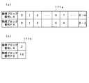
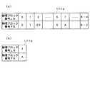
以下、ブロック管理手段170について詳細に説明する。論物変換テーブル171は図8に一例を示すように、論物変換主テーブル171aと論物変換補助テーブル171bを有している。論物変換主テーブル171aでは、論理ブロック番号LB0の論理ブロックが物理ブロック番号PB3の物理ブロックに、論理ブロック番号LB1の論理ブロックが物理ブロック番号PB6の物理ブロックにマッピングされていることを示している。また論理ブロック番号LBL及びLB(L+1)の論理ブロックには、対応する物理ブロックとして無効な番号Aが記録されている。これはこれらの論理ブロックLBL,LB(L+1)にデータが書かれていないことを示している。 Hereinafter, the block management means 170 will be described in detail. As shown in FIG. 8, the logical-physical conversion table 171 includes a logical-physical conversion main table 171a and a logical-physical conversion auxiliary table 171b. The logical-physical conversion main table 171a indicates that the logical block with the logical block number LB0 is mapped to the physical block with the physical block number PB3, and the logical block with the logical block number LB1 is mapped to the physical block with the physical block number PB6. . In addition, in the logical blocks having the logical block numbers LBL and LB (L + 1), an invalid number A is recorded as the corresponding physical block. This indicates that no data is written in these logical blocks LBL and LB (L + 1).
また図8(b)に示す論物変換補助テーブル171bは、1つの論理ブロックに複数の物理ブロックが割り当てられたときに追加の物理ブロックの番号を保持するものである。この論物変換補助テーブル171bへの登録数は少なくとも1つとし、ここでは登録数が1の場合について説明する。 Further, the logical-physical conversion auxiliary table 171b shown in FIG. 8B holds the numbers of additional physical blocks when a plurality of physical blocks are assigned to one logical block. The number of registrations in the logical-physical conversion auxiliary table 171b is at least one, and here, a case where the number of registrations is 1 will be described.
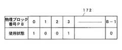
ブロック管理手段170では、空きブロック管理テーブル172を管理しながら半導体記憶装置全体のブロック管理を実施している。図9は空きブロック管理テーブル172の一例であり、各物理ブロックの使用状態を示す。使用状態が1の物理ブロックは使用中、0の物理ブロックは空きブロックで新たに使用できることを示す。 The block management means 170 performs block management of the entire semiconductor memory device while managing the free block management table 172. FIG. 9 shows an example of the free block management table 172, which shows the usage status of each physical block. A physical block whose usage status is 1 indicates that it is in use, and a physical block whose status is 0 is a free block and can be newly used.
ブロック管理手段170は、電源が供給されると、空きブロック管理テーブル172の全ブロックを空き状態に初期化し、不良ブロックを使用済みに更新する。不良ブロックの管理は発明の本質から外れるので詳細な説明はしないが、フラッシュメモリの固定位置に書き込んでおく。次いで論物変換テーブル171を読み出し、これに基づいて使用されている物理ブロックを使用済みに更新する。また書き込み済みの論理ブロックを書き換えるときは、空きブロック管理テーブル172よりランダムにサーチして空き物理ブロックを新規物理ブロックとして選択する。選択された物理ブロックにデータが書き込まれると、そのブロックを使用済みブロックに、当該論理ブロックに対応していた直前の物理ブロックを空きブロックに更新する。 When the power is supplied, the
ホスト機器200Aのファイルを半導体記憶装置100Aに転送して書き込む処理の概略について、図10を用いて説明する。まず、ホスト機器200A上のアプリケーションが半導体記憶装置100Aにファイルを書き込む場合、ファイルシステムが半導体記憶装置100Aへ書き込む論理アドレスを求める。半導体記憶装置100Aへ書き込む際には、ホスト機器200A内のデータバッファ250のサイズや半導体記憶装置100Aで受けられる転送サイズなどの制約により、ファイルを小さなサイズに分割して半導体記憶装置100Aへ書き込む。図10ではファイルを1から6の6つのブロックに分割して書き込みを行う。図10の半導体記憶システムは、ホスト機器200Aのコマンド分割手段240により分割後、転送すべきデータをデータバッファ250に蓄積し、コマンド発行手段220で書き込みコマンドを生成して、外部インターフェイス手段210経由でコマンドを発行する。ホスト機器200Aと半導体記憶装置100A間でデータ転送が完了して、半導体記憶装置100A内のフラッシュメモリ140へのデータの書き込みが完了すれば、データバッファ250内のデータを開放し、次の転送へ移行する。図10に示す1から6の6つのブロックの転送が完了すれば、ファイルの転送が完了したことになる。 An outline of processing for transferring and writing the file of the
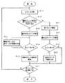
次にホスト機器200Aの全体動作について、以下詳細に説明する。図11はホスト機器200Aの動作を示すフローチャートである。ここではホスト機器200Aは半導体記憶装置100Aにファイル1,2,3・・・を順次記録する場合について説明する。図11において処理を開始すると、図10に示すようにコマンド分割手段240により、コマンドをファイルの転送サイズに分割する(S11)。分割の手順としては、半導体記憶装置100Aから、メモリ情報通知手段180を経由して、フラッシュメモリ140の情報を取り出す。コマンド分割手段240は、ブロック境界管理手段260に保持している物理ブロックサイズをもとに書き込むべきファイルを物理ブロックの境界で分割する。次にデータを書き込もうとしている物理ブロックに既に書き込まれたデータとこれから転送するデータがデータバッファ250に保持されているかを確認する(S12)。データが存在する場合は、分割したデータを含む書き込みコマンドを半導体記憶装置100Aに対して発行する(S13)。エラーが発生することなく書き込みが終了した場合は、転送を終了した物理ブロック単位の分のデータがデータバッファ250にあれば、これを解放する(S16)。次いでS17に進み、全ファイルの書き込みが終了したかどうか判断する。全ファイルの書き込みが終了していない場合には、S11へ戻り、再度ファイルの残り部分を書き込む。ファイルの書き込みが完了した場合には、転送を終了する。エラーが発生した場合にはS14からS15に進み、当該コマンドで転送したデータを含む物理ブロック全体のデータを再度書き込む。こうすればエラーが生じた物理ブロック内のデータを復旧することができる。 Next, the overall operation of the
一方、S12でデータを書き込もうとしている物理ブロックに対して既に書き込まれたデータがデータバッファ250に保持されていない場合は、S21に進む。この場合は新物理ブロックを要求するコマンドを発行し、書き込みコマンドを発行する(S21,S22)。この書き込みによってエラーが発生したかどうかを判断する。エラーが発生しない場合には、S17に進む。エラーが発生した場合には、当該コマンドで書き込めなかったデータのみ再書き込みを行う。 On the other hand, if the data already written to the physical block to which data is to be written in S12 is not held in the
さて、ホスト機器200Aが半導体記憶装置100Aに書き込みコマンドを出すと、アドレス変換手段120は、ホスト機器200Aが書き込みを要求した論理アドレスを実際に書き込みを行う物理アドレスに変換する。その物理ブロックに空きがあれば追記書き込みを行い、空きがなければ新物理ブロックを確保する。新物理ブロックの確保が必要であれば、ブロック管理手段170は空きブロック管理テーブル172をサーチして新規物理ブロックを確保する。データ書き込み手段130は、新たに物理ブロックが確保された後に、フラッシュメモリ140に対して書き込みを行う。 When the
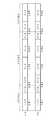
次にS13以降の処理についてより詳しく図12を用いて動作例と共に説明する。図12の上図が論理アドレス空間LAであり、下図がこれに対応する物理アドレス空間PAを示す概念図である。まずファイル1の(1−1)の部分を論理ブロックLB1に割り当て、このデータを物理ブロックPB1に書き込み、ファイル1の(1−2)の部分を論理ブロックLB2に割り当て、このデータを物理ブロックPB2の前半部分に書き込む。続いてファイル2を書き込む場合に、(2−1)の部分を論理ブロックLB2に割り当て、物理ブロックPB2の後半部分に書き込む。このときS12ではデータバッファ250が直前のファイル1の(1−2)部分のデータを保持しているかどうかを確認しており、保持していれば(2−1)のデータを物理ブロックPB2の後半部分に追記する。この書き込み中にエラーが発生した場合には、ファイル1,2の(1−2)と(2−1)の部分を再度書き込むことにより、物理ブロックのデータの安全性は確保される。データ解放判断手段270は、図12のファイル1の(1−2)の転送が完了した時点ではデータバッファ250のデータの解放を行わずに、次のファイル2の(2−1)の書き込み時のエラーに備えて、データを保存したままにしておく。ファイル2の(2−1)の書き込みが完了した時点で、データ解放判断手段270は、ファイル1の(1−2)及びファイル2の(2−1)のデータを解放すると判断し、データバッファ250内のデータを解放する(S16)。 Next, the processing after S13 will be described in more detail with an operation example using FIG. The upper diagram of FIG. 12 is the logical address space LA, and the lower diagram is a conceptual diagram showing the physical address space PA corresponding thereto. First, the (1-1) portion of the
これについて、図13を用いて更に詳細に説明する。図13では左側の論理アドレス空間の論理ブロックLB2の一部に、図示のようにファイル1の(1−2)部分が既に書き込み済みであり、論理ブロックLB2に対応する物理ブロックPB2のページ0から(K−2)までにファイル1の(1−2)部分が書き込まれているものとする。この場合は物理ブロックPB2にファイル(2−1)追記して書き込む。 This will be described in more detail with reference to FIG. In FIG. 13, the (1-2) portion of the
更に、S21以の処理についてより詳しく図14を用いて動作例と共に説明する。図12と同様にファイル1の(1−1)の部分を論理ブロックLB1に割り当て、このデータを物理ブロックPB1に書き込み、ファイル1の(1−2)の部分を論理ブロックLB2に割り当て、このデータを物理ブロックPB2の前半部分に書き込む。ファイル1書き込み後に、ホスト機器200Aと半導体記憶装置100Aの電源がオフとなり、その後、再度電源が投入され、ファイル2を書き込むものとする。電源オフによりホスト機器200Aのデータバッファ250にはファイル1の(1−2)の部分のデータは消えている。従ってS12ではデータが存在しないと判断され、S21に進む。この場合には、ファイル2の(2−1)の書き込みに先立って、新たな物理ブロックを要求する。そして論理ブロックLB2にファイル2の(2−2)に対してデータを書き込む。半導体記憶装置100Aは新物理ブロック、例えばPB10を抽出し、このブロックにファイル2のデータ(2−1)部分を書き込む。この書き込み中にエラーが発生したとしても、物理ブロックPB2に書き込まれているファイル1の(1−2)部分のデータには影響がない。従ってファイル2の(2−1)部分のみ再度書き込みを行うことで復旧することができる。 Further, the processing after S21 will be described in more detail with an operation example using FIG. As in FIG. 12, the (1-1) portion of the
この方法によれば、電源がオンとなる以前に書き込まれたファイルを破壊しないで書き込むことができる。これについて、図15を用いて更に詳細に説明する。図15では左側の論理アドレス空間の論理ブロックLB2の一部に、図示のようにファイル1の(1−2)部分が既に書き込み済みであり、論理ブロックLB2に対応する物理ブロックPB2のページ0から(K−2)までにファイル1の(1−2)部分が書き込まれているものとする。この場合の論物変換テーブル171の状態の変化を説明する。図16は図15の物理ブロックPB2が登録されていることを示す論物変換テーブルである。即ち論物変換主テーブル171aの論理ブロック番号LB2は物理アドレス空間の物理ブロックPB2に割り当てられている。 According to this method, a file written before the power is turned on can be written without being destroyed. This will be described in more detail with reference to FIG. In FIG. 15, the (1-2) portion of the
さてこの状態で論理ブロックLB2にファイル(2−1)を追記する。この場合は物理ブロックPB2へ追記はせずに新たに物理ブロックPB10を確保し、この物理ブロックPB10にファイル(2−1)を書き込む。図16(b)は、論理ブロックが2つの物理ブロックから構成される場合に、利用する論物変換補助テーブル171bであり、このテーブルに示すように論理ブロックLB2が右下側の物理ブロックPB10にも割り当てられている。こうすれば、ファイル(2−1)の書き込み中に突然の電源断が発生しても、ファイル1の(1−2)が保持されている物理ブロックとは異なるために、ファイル1の破壊を回避することができる。 In this state, the file (2-1) is added to the logical block LB2. In this case, a new physical block PB10 is secured without adding to the physical block PB2, and the file (2-1) is written to the physical block PB10. FIG. 16B shows a logical-physical conversion auxiliary table 171b to be used when the logical block is composed of two physical blocks. As shown in this table, the logical block LB2 is changed to the physical block PB10 on the lower right side. Is also assigned. In this way, even if a sudden power interruption occurs while the file (2-1) is being written, it is different from the physical block in which (1-2) of
データバッファ250は、通常限られた領域であり、ホスト機器200Aの処理に応じて頻繁に、確保と、解放が行われる。本発明では、エラー発生時に備えて、転送中のデータに加えて、エラーの伝搬がおよぶ領域のデータもデータバッファ250に保持しているが、データバッファ250の領域が足りなくなった場合には、エラーの伝搬がおよぶ領域のデータの解放を優先する。データが解放されて、データバッファ250から消去されてしまったかどうかは、ホスト機器200Aのソフトウエアが管理するために、判断可能である。従って図14において、ファイル2の(2−4)の書き込み後に、ホスト機器200Aでデータバッファ250を利用する処理が発生して、(2−4)のデータが解放されたとする。この場合、つづくファイル3の(3−1)部分の書き込みの時点ではデータバッファ250には(2−4)のデータは存在しない。従ってS21以降の処理に進み、新たな物理ブロックを要求する。半導体記憶装置100Aは新物理ブロック、例えばPB11を抽出し、このブロックにファイル3のデータ(3−1)部分を書き込む。 The
かかる構成によれば、ホスト機器側でエラー伝搬するデータを保持しておくことにより、新規に物理ブロックを確保する場合を少なくすることができる。過去のデータの破壊が許されない場合の書き込みにのみ新規に物理ブロックを確保して書き込みを行うことにより、転送速度・書き換え回数への影響を少なくすることが可能になる。 According to such a configuration, it is possible to reduce a case where a physical block is newly secured by holding data that propagates an error on the host device side. It is possible to reduce the influence on the transfer speed and the number of rewrites by newly securing a physical block only for writing when past data destruction is not permitted.
物理ブロックに余裕があるにもかかわらず新規物理ブロックを確保してデータを書き込んだ場合には、1つの論理ブロックに対して2つの物理ブロックが必要になり、容量的に課題がある。このために、データの書き込みや読み出しを行っていないときに、新たな物理ブロックを確保して、2つの物理ブロックから有効なページのみを集めて1つの物理ブロックに集約する必要がある。集約処理について図17,図18を用いて説明する。集約処理では、図17の右側に示すように、新たに物理ブロック、ここではPB20を確保する。そして同一の論理ブロックLB2に対応する2つの物理ブロックPB2と物理ブロックPB10の有効なページのデータを集めて、物理ブロックPB20にコピーをする。コピーが完了すると、図18のように論物変換主テーブル171aでは論理ブロックLB2に対して物理ブロックPB20を登録すると共に、論物変換補助テーブル171bの論理ブロックLB2に無効番号であるAを登録する。 When new physical blocks are secured and data is written even though there is room in the physical blocks, two physical blocks are required for one logical block, and there is a problem in capacity. For this reason, when data is not written or read, it is necessary to secure a new physical block, collect only valid pages from two physical blocks, and consolidate them into one physical block. The aggregation process will be described with reference to FIGS. In the aggregation process, a new physical block, here PB20, is secured as shown on the right side of FIG. Data of valid pages of the two physical blocks PB2 and PB10 corresponding to the same logical block LB2 are collected and copied to the physical block PB20. When the copying is completed, as shown in FIG. 18, in the logical-physical conversion main table 171a, the physical block PB20 is registered with respect to the logical block LB2, and the invalid number A is registered with the logical block LB2 of the logical-physical conversion auxiliary table 171b. .
(第2の実施の形態)
次に本発明の第2の実施の形態について説明する。図19Aはこの実施の形態の半導体記憶装置100Bの構成であり、図19Bはホスト機器200Bの構成を示す。半導体記憶装置100Bは図19Aに示すようにデータ書き込み手段130にエラー伝搬検出手段190が接続される。エラー伝搬検出手段190はデータの書き込みがフラッシュメモリの第2ページに書き込まれ、伝搬の可能性が生じる書き込みかどうかを判別し、実際にエラーが生じればエラーによる伝搬の可能性を外部インターフェイス手段110を介してホスト機器200Bに伝えるものである。又ホスト機器200Bのコマンド発行手段280は外部インターフェイス手段210を介してエラーによる伝搬の可能性が伝えられた場合に、物理ブロックの単位で再書き込みをするコマンドを発行するものである。その他の動作についてはコマンド発行手段220と同様である。(Second Embodiment)
Next, a second embodiment of the present invention will be described. FIG. 19A shows the configuration of the
次に図20のフローチャートを用いて第2の実施の形態の動作について説明する。図20において前述した第1の実施の形態と同一部分は同一のステップ番号を付して詳細な説明を省略する。ステップS14においてエラーがあればホスト機器200Bはエラー伝搬のデータを待受ける。エラー伝搬検出手段190は、エラーがあった場合にセル共有によるエラーが伝搬する範囲を特定して、書き込みエラー時に、セル共有によるエラー伝搬が起こったかどうかをホスト機器200に通知する。S18において、ホスト機器200のコマンド発行手段280はセル共有によるエラー伝搬が起こっていない場合には、S24に進んでエラーが発生した書き込みコマンドのみを書き込みコマンドとして再発行する。一方、セル共有によるエラー伝搬が起こっている場合には、S15に進んで物理ブロック全体の書き込みコマンドを発行する。こうすることにより、再送するデータを最適化することが可能になる。 Next, the operation of the second embodiment will be described using the flowchart of FIG. In FIG. 20, the same parts as those of the first embodiment described above are denoted by the same step numbers, and detailed description thereof is omitted. If there is an error in step S14, the
尚この実施の形態では、第2ページの書き込みがあり、且つエラーがあった場合に、エラーの伝搬の可能性があるとしてホスト機器にエラー伝搬を検出するようにしているが、実際に第2ページにおいて伝搬が生じたかどうかを判別してホスト機器に伝えるようにしてもよい。この場合にはテーブルにエラーの伝搬するアドレスを保持しておき、エラー伝搬する可能性のあるアドレスをフラッシュメモリの書き込みアドレスから検出すれば、エラーが発生したときのアドレスから伝搬するアドレスを特定して伝搬が影響するかを判断することができる。 In this embodiment, when there is a second page write and there is an error, error propagation is detected by the host device as there is a possibility of error propagation. You may make it discriminate | determine whether propagation occurred in the page and tell it to a host apparatus. In this case, the error propagation address is stored in the table, and if the error propagation possibility address is detected from the flash memory write address, the address propagation from the address when the error occurs is specified. Thus, it is possible to determine whether propagation is affected.
なお、ホスト機器から半導体記憶装置に映像を記録する場合であっても、ホスト機器がパーソナルコンピュータ(PC)であってファイルを書き込む場合も、同等の効果を得ることが可能になる。 Note that even when video is recorded from the host device to the semiconductor storage device, the same effect can be obtained even when the host device is a personal computer (PC) and a file is written.
また本願の第1,第2の実施の形態では、多値フラッシュメモリの1つのメモリセルに格納するビット数を2ビットとしたが、更に状態を増加させ1メモリセルに3ビット以上格納できるフラッシュメモリにも適応可能であることはいうまでもない。 In the first and second embodiments of the present application, the number of bits stored in one memory cell of the multi-level flash memory is 2 bits. However, the flash can be stored in more than 3 bits in one memory cell by increasing the state. Needless to say, it is also applicable to memory.
更に、フラッシュメモリのみならず、他の不揮発性メモリに適応しても同様の効果が得られることはいうまでもない。また、ホスト機器から転送されるデータを記録する半導体記憶装置として説明したが、ホスト機器内に半導体記憶装置を備えた装置であっても同様の効果が得られることはいうまでもない。 Furthermore, it goes without saying that the same effect can be obtained by adapting not only to the flash memory but also to other nonvolatile memories. Further, although the semiconductor memory device that records data transferred from the host device has been described, it is needless to say that the same effect can be obtained even if the device includes the semiconductor memory device in the host device.
尚ここでは物理ブロックを消去の最小の単位として説明しているが、物理ブロックは論理ブロックに対応するブロックとして規定されるものであるため、物理ブロックのサイズと消去の単位とが異なるものとしてもよい。この場合には1つの物理ブロックを消去の最小単位の整数倍のサイズとすることもできる。この場合には各消去の単位毎に現在の状態を空きブロック管理テーブル等で管理する必要がある。尚消去の単位は多値フラッシュメモリにおいてはメモリの共有関係を有するグループとして考えることができる。 Although the physical block is described as the minimum unit of erasure here, the physical block is defined as a block corresponding to the logical block, so the physical block size and the erasure unit may be different. Good. In this case, one physical block can have a size that is an integral multiple of the minimum unit of erasure. In this case, it is necessary to manage the current state for each erasing unit using an empty block management table or the like. The unit of erasure can be considered as a group having a shared memory relationship in the multi-level flash memory.
本発明の半導体記憶装置は、セル共有部分のデータの破壊による影響を最小限にとどめることができるので、信頼性を必要とされる業務用分野等で有用である。 Since the semiconductor memory device of the present invention can minimize the influence caused by the destruction of the data in the cell shared portion, it is useful in the field of business requiring reliability.
100A,100B 半導体記憶装置
110 外部インターフェイス手段
120 アドレス変換手段
130 データ書き込み手段
140 フラッシュメモリ
150 データ読み出し手段
160 コマンド解析手段
170 ブロック管理手段
171 論物変換テーブル
171a 論物変換主テーブル
171b 論物変換補助テーブル
172 空きブロック管理テーブル
180 メモリ情報通知手段
190 エラー伝搬検出手段
200A,200B ホスト機器
210 外部インターフェイス手段
220,280 コマンド発行手段
230 新ブロック書き込み要求手段
240 コマンド分割手段
250 データバッファ
260 ブロック境界管理手段
270 データ解放判断手段
100A, 100B
Claims (13)
Translated fromJapanese前記半導体記憶装置は、
複数の物理ブロックにより構成され、書き込みエラーが既に書き込まれた物理ブロックのデータに伝播する不揮発性メモリと、
前記ホスト機器より与えられる論理アドレスを前記不揮発性メモリの物理アドレスに変換するアドレス変換手段と、
前記不揮発性メモリへデータの書き込みを行うデータ書き込み手段と、
前記不揮発性メモリからデータの読み出しを行うデータ読み出し手段と、
ホスト機器が発行するコマンドにかかる論理ブロックと前記不揮発性メモリの物理ブロックとの対応を記録してアドレス管理を行う論物変換テーブルを備えたブロック管理手段と、
前記不揮発性メモリのメモリ情報を通知するメモリ情報通知手段と、を備え、
前記ホスト機器は、
前記半導体記憶装置のメモリ情報通知手段から通知されたメモリ情報に基づいて書き込み単位となる物理ブロックの境界を管理するブロック境界管理手段と、
前記ブロック境界管理手段からの物理ブロックへのアクセス単位をもとに書き込むべきデータと書き込みコマンドを分割するコマンド分割手段と、
書き込みコマンドの発行時に書き込むべきデータ及び前記書き込みコマンドに対するエラー発生時にエラー伝播が及ぶ領域のデータを保存するデータバッファと、
前記半導体記憶装置に書き込みコマンドを発行すると共に、半導体記憶装置への書き込み時に書き込みエラーが発生した場合には、書き込みエラーが発生したブロックに書き込むべきデータを前記データバッファより読み出して書き込みコマンドを再発行するコマンド発行手段と、
前記データバッファに保存しているデータを開放するかどうかを書き込みエラーが伝搬する範囲に基づいて判断するデータ解放判断手段と、を備える半導体記憶システム。A semiconductor storage system comprising a host device and a semiconductor storage device,
The semiconductor memory device
A non-volatile memory configured by a plurality of physical blocks, in whicha write error is propagated to the data of the already written physical block ;
Address conversion means for converting a logical address given by the host device into a physical address of the nonvolatile memory;
Data writing means for writing data to the nonvolatile memory;
Data reading means for reading data from the nonvolatile memory;
A block management means comprising a logical-physical conversion table for performing address management by recording a correspondence between a logical block relating to a command issued by a host device and a physical block of the nonvolatile memory;
Memory information notification means for notifying the memory information of the nonvolatile memory,
The host device is
Block boundary management means for managing the boundaries of physical blocks as write units based on the memory information notified from the memory information notification means of the semiconductor memory device;
Command dividing means for dividing data to be written and a write command based on an access unit to the physical block from the block boundary management means;
A data buffer for storingdata to be written when a write command is issuedand data inan area where error propagation extends when an error occurs with respect to the write command ;
Issuing a write command to the semiconductor memory device, and if a write error occurs when writing to the semiconductor memory device, read the data to be written to the block in which the write error has occurred from the data buffer and reissue the write command Command issuing means to perform,
A data release determining means for determining whether to release the data stored in the data buffer based on a range in which a write error propagates;
物理ブロック単位でデータの転送が完了した時点で前記データバッファのデータを解放すると判断する請求項1記載の半導体記憶システム。The data release determining means is
2. The semiconductor memory system according to claim 1, wherein when the data transfer is completed in units of physical blocks, it is determined to release the data in the data buffer.
エラーが発生したときに、前記データバッファに物理ブロック単位のデータがあれば物理ブロック全体の書き込みコマンドを再発行し、前記データバッファに物理ブロック単位のデータがなければエラーになった当該コマンドを再発行する請求項1又は2記載の半導体記憶システム。The command issuing means includes
When an error occurs, if there is data in physical block units in the data buffer, a write command for the entire physical block is reissued. If there is no data in physical block units in the data buffer, the command in error is reissued. 3. The semiconductor storage system according to claim 1, which is issued.
データの書き込み時に、前記半導体記憶装置にそのデータが書き込まれるブロックの記録済みデータを前記データバッファに保持していないときに、新ブロックへの書き込みを要求する新ブロック書き込み要求手段をさらに備えた請求項1〜3のいずれか1項記載の半導体記憶システム。The host device is
Claims further comprising: a new block write request means for requesting writing to a new block when data recorded is not held in the data buffer when the data is written to the semiconductor memory device when the data is written. Item 4. The semiconductor storage system according to any one of Items 1 to 3.
電源投入後の最初の書き込みコマンドを発行する際に新ブロックへの書き込みを要求する請求項4記載の半導体記憶システム。The new block write request means includes
5. The semiconductor memory system according to claim 4, wherein a write to a new block is requested when a first write command after power-on is issued.
書き込みコマンドが書き込みエラーになった場合に、当該コマンドのアドレス領域以外に影響が及ぶかを判断してエラーステータスとして前記ホスト機器に通知するエラー伝搬検出手段を備え、
前記コマンド発行手段は、
エラーステータスが当該コマンドのアドレス領域以外に影響が及ぶ場合には所定の物理ブロック全体の書き込みコマンドを再発行し、
エラーステータスが当該コマンドのアドレス領域以外に影響が及ばない場合にはエラーになった当該コマンドを再発行する請求項1又は2記載の半導体記憶システム。The semiconductor memory device
When a write command results in a write error, it comprises an error propagation detection means for determining whether it affects other than the address area of the command and notifying the host device as an error status,
The command issuing means includes
If the error status affects other than the address area of the command, re-issue the write command for the entire specified physical block,
3. The semiconductor memory system according to claim 1, wherein when the error status does not affect other than the address area of the command, the command in error is reissued.
前記メモリの最小の消去単位及びその整数倍の消去単位のいずれかである請求項1〜7のいずれか1項記載の半導体記憶システム。The physical block is
8. The semiconductor memorysystem according to claim 1, wherein the semiconductor memorysystem is one of a minimum erasing unit of the memory and an erasing unit that is an integral multiple of the minimum erasing unit.
前記半導体記憶装置のメモリ情報に基づいて書き込み単位となる物理ブロックの境界を管理するブロック境界管理手段と、
前記ブロック境界管理手段からの物理ブロックへのアクセス単位をもとに書き込むべきデータと書き込みコマンドを分割するコマンド分割手段と、
書き込みコマンドの発行時に書き込むべきデータ及び前記書き込みコマンドに対するエラー発生時にエラー伝播が及ぶ領域のデータを保存するデータバッファと、
前記半導体記憶装置に書き込みコマンドを発行すると共に、半導体記憶装置への書き込み時に書き込みエラーが発生した場合には、書き込みエラーが発生したブロックに書き込むべきデータを前記データバッファより読み出して書き込みコマンドを再発行するコマンド発行手段と、
前記データバッファに保存しているデータを開放するかどうかを書き込みエラーが伝搬する範囲に基づいて判断するデータ解放判断手段と、を具備するホスト機器。A host device connected toa semiconductor storage devicehaving a non-volatile memory that is configured by a plurality of physical blocks and propagates data of a physical block in which a write error has already been written ,
Block boundary management means for managing a boundary of a physical block as a writing unit based on memory information of the semiconductor storage device;
Command dividing means for dividing data to be written and a write command based on an access unit to the physical block from the block boundary management means;
A data buffer for storingdata to be written when a write command is issuedand data inan area where error propagation extends when an error occurs with respect to the write command ;
Issuing a write command to the semiconductor memory device, and if a write error occurs when writing to the semiconductor memory device, read the data to be written to the block in which the write error has occurred from the data buffer and reissue the write command Command issuing means to perform,
A host device comprising: a data release determining means for determining whether to release the data stored in the data buffer based on a range in which a write error propagates.
物理ブロック単位でデータの転送が完了した時点で前記データバッファのデータを解放すると判断する請求項9記載のホスト機器。The data release determining means is
The host device according to claim 9, wherein the host device determines to release the data in the data buffer when the data transfer is completed in units of physical blocks.
エラーが発生したときに、前記データバッファに物理ブロック単位のデータがあれば物理ブロック全体の書き込みコマンドを再発行し、前記データバッファに物理ブロック単位のデータがなければエラーになった当該コマンドを再発行する請求項9又は10記載のホスト機器。The command issuing means includes
When an error occurs, if there is data in physical block units in the data buffer, a write command for the entire physical block is reissued. If there is no data in physical block units in the data buffer, the command in error is reissued. The host device according to claim 9 or 10, which is issued.
データの書き込み時に、前記半導体記憶装置にそのデータが書き込まれるブロックの記録済みデータを前記データバッファに保持していないときに、新ブロックへの書き込みを要求する新ブロック書き込み要求手段をさらに備えた請求項9〜11のいずれか1項記載のホスト機器。The host device is
Claims further comprising: a new block write request means for requesting writing to a new block when data recorded is not held in the data buffer when the data is written to the semiconductor memory device when the data is written. Item 12. The host device according to any one of Items 9 to 11.
電源投入後の最初の書き込みコマンドを発行する際に新ブロックへの書き込みを要求する請求項12記載のホスト機器。The new block write request means includes
13. The host device according to claim 12, wherein a write to a new block is requested when a first write command after power-on is issued.
Priority Applications (2)
| Application Number | Priority Date | Filing Date | Title |
|---|---|---|---|
| JP2009001442AJP5300496B2 (en) | 2009-01-07 | 2009-01-07 | Semiconductor memory device, host device, and semiconductor memory system |
| US12/652,790US8352807B2 (en) | 2009-01-07 | 2010-01-06 | Semiconductor memory device, host device and semiconductor memory system |
Applications Claiming Priority (1)
| Application Number | Priority Date | Filing Date | Title |
|---|---|---|---|
| JP2009001442AJP5300496B2 (en) | 2009-01-07 | 2009-01-07 | Semiconductor memory device, host device, and semiconductor memory system |
Publications (2)
| Publication Number | Publication Date |
|---|---|
| JP2010160605A JP2010160605A (en) | 2010-07-22 |
| JP5300496B2true JP5300496B2 (en) | 2013-09-25 |
Family
ID=42312489
Family Applications (1)
| Application Number | Title | Priority Date | Filing Date |
|---|---|---|---|
| JP2009001442AActiveJP5300496B2 (en) | 2009-01-07 | 2009-01-07 | Semiconductor memory device, host device, and semiconductor memory system |
Country Status (2)
| Country | Link |
|---|---|
| US (1) | US8352807B2 (en) |
| JP (1) | JP5300496B2 (en) |
Cited By (1)
| Publication number | Priority date | Publication date | Assignee | Title |
|---|---|---|---|---|
| US10553262B2 (en) | 2017-12-13 | 2020-02-04 | Toshiba Memory Corporation | Memory system and memory device |
Families Citing this family (8)
| Publication number | Priority date | Publication date | Assignee | Title |
|---|---|---|---|---|
| KR101178562B1 (en)* | 2010-11-02 | 2012-09-03 | 에스케이하이닉스 주식회사 | Command control circuit and semiconductor device incluging the same and control method of command |
| JP2013052556A (en)* | 2011-09-02 | 2013-03-21 | Canon Inc | Image forming apparatus, control method of the same, and program |
| US9971522B2 (en) | 2014-07-21 | 2018-05-15 | Toshiba Memory Corporation | Memory system and method |
| US20160054943A1 (en)* | 2014-08-22 | 2016-02-25 | Kabushiki Kaisha Toshiba | Information processing apparatus |
| JP7131053B2 (en)* | 2018-04-24 | 2022-09-06 | 富士通株式会社 | Storage device, information processing program and information processing system |
| JP7484633B2 (en)* | 2020-09-30 | 2024-05-16 | 株式会社デンソー | Shared storage management device and shared storage management method |
| CN112948217B (en)* | 2021-03-29 | 2023-01-13 | 腾讯科技(深圳)有限公司 | Server repair checking method and device, storage medium and electronic equipment |
| US12292794B2 (en)* | 2023-01-18 | 2025-05-06 | Micron Technology, Inc. | Techniques for managing memory exception handling |
Family Cites Families (14)
| Publication number | Priority date | Publication date | Assignee | Title |
|---|---|---|---|---|
| JPH06139123A (en)* | 1992-10-29 | 1994-05-20 | Toshiba Corp | Storage device for file |
| JPH1091539A (en)* | 1996-09-12 | 1998-04-10 | Sony Corp | Data storage |
| US5937434A (en)* | 1997-02-14 | 1999-08-10 | Intel Corporation | Method of managing a symmetrically blocked nonvolatile memory having a bifurcated storage architecture |
| JP3618529B2 (en)* | 1997-11-04 | 2005-02-09 | 富士通株式会社 | Disk array device |
| US6205548B1 (en)* | 1998-07-31 | 2001-03-20 | Intel Corporation | Methods and apparatus for updating a nonvolatile memory |
| JP2000100156A (en)* | 1998-09-25 | 2000-04-07 | Fujitsu Ltd | Cell information writing method for semiconductor memory device and semiconductor memory device |
| JP2000267941A (en)* | 1999-03-19 | 2000-09-29 | Fujitsu Ltd | Store error compensator |
| US7020758B2 (en)* | 2002-09-18 | 2006-03-28 | Ortera Inc. | Context sensitive storage management |
| JP2004288283A (en)* | 2003-03-20 | 2004-10-14 | Hitachi Ltd | Information recording format, information recording / reproducing encoding method / circuit, magnetic disk recording / reproducing device using the same, information recording / reproducing device, and information communication device |
| CN100470585C (en)* | 2004-03-31 | 2009-03-18 | 松下电器产业株式会社 | Memory Cards and Memory Card Systems |
| JP4842563B2 (en)* | 2005-05-16 | 2011-12-21 | パナソニック株式会社 | MEMORY CONTROLLER, NONVOLATILE MEMORY DEVICE, NONVOLATILE MEMORY SYSTEM, AND DATA WRITE METHOD |
| CN101194238B (en)* | 2005-06-24 | 2010-05-19 | 松下电器产业株式会社 | Memory controller, nonvolatile storage device, nonvolatile storage system, and data writing method |
| DE102008022831B4 (en)* | 2008-05-08 | 2015-09-10 | Fujitsu Technology Solutions Intellectual Property Gmbh | Working method for a storage subsystem and devices for carrying out the working method |
| US8327062B2 (en)* | 2008-12-09 | 2012-12-04 | Infineon Technologies Ag | Memory circuit and method for programming in parallel a number of bits within data blocks |
- 2009
- 2009-01-07JPJP2009001442Apatent/JP5300496B2/enactiveActive
- 2010
- 2010-01-06USUS12/652,790patent/US8352807B2/enactiveActive
Cited By (1)
| Publication number | Priority date | Publication date | Assignee | Title |
|---|---|---|---|---|
| US10553262B2 (en) | 2017-12-13 | 2020-02-04 | Toshiba Memory Corporation | Memory system and memory device |
Also Published As
| Publication number | Publication date |
|---|---|
| US20100174951A1 (en) | 2010-07-08 |
| US8352807B2 (en) | 2013-01-08 |
| JP2010160605A (en) | 2010-07-22 |
Similar Documents
| Publication | Publication Date | Title |
|---|---|---|
| JP5300496B2 (en) | Semiconductor memory device, host device, and semiconductor memory system | |
| JP5612514B2 (en) | Nonvolatile memory controller and nonvolatile storage device | |
| CN105808156B (en) | Method for writing data into solid state disk and solid state disk | |
| US9753653B2 (en) | High-priority NAND operations management | |
| JP4256175B2 (en) | Nonvolatile semiconductor memory | |
| JP5405513B2 (en) | MEMORY SYSTEM, NONVOLATILE MEMORY DEVICE, NONVOLATILE MEMORY DEVICE CONTROL METHOD, AND PROGRAM | |
| JP4524309B2 (en) | Memory controller for flash memory | |
| CN111414342B (en) | Storage device and data processing method thereof | |
| US20160118132A1 (en) | Low Impact Read Disturb Handling | |
| US20140075100A1 (en) | Memory system, computer system, and memory management method | |
| CN101681312A (en) | memory system | |
| CN107608628A (en) | Flash memory controller | |
| JP2009205555A (en) | Memory system | |
| JP5073402B2 (en) | MEMORY CONTROLLER, NONVOLATILE MEMORY DEVICE USING THE SAME, AND NONVOLATILE MEMORY SYSTEM | |
| JP4866117B2 (en) | Nonvolatile storage device, data writing method thereof, nonvolatile storage system, and memory controller | |
| JP5592478B2 (en) | Nonvolatile storage device and memory controller | |
| TWI540428B (en) | Data writing method, memory controller and memory storage apparatus | |
| TW202011194A (en) | Flash memory controller and associated electronic device | |
| US9778862B2 (en) | Data storing method for preventing data losing during flush operation, memory control circuit unit and memory storage apparatus | |
| KR101070511B1 (en) | Solid state drive controller and method for operating of the solid state drive controller | |
| JP2012068765A (en) | Memory controller, flash memory system with memory controller, and control method of flash memory | |
| JP5264459B2 (en) | Semiconductor memory device | |
| JP4551938B2 (en) | Memory system | |
| JP4558052B2 (en) | Memory system | |
| US12373336B2 (en) | Storage system and method of operating the storage system |
Legal Events
| Date | Code | Title | Description |
|---|---|---|---|
| A621 | Written request for application examination | Free format text:JAPANESE INTERMEDIATE CODE: A621 Effective date:20111101 | |
| RD03 | Notification of appointment of power of attorney | Free format text:JAPANESE INTERMEDIATE CODE: A7423 Effective date:20120207 | |
| RD04 | Notification of resignation of power of attorney | Free format text:JAPANESE INTERMEDIATE CODE: A7424 Effective date:20120210 | |
| A977 | Report on retrieval | Free format text:JAPANESE INTERMEDIATE CODE: A971007 Effective date:20130411 | |
| A131 | Notification of reasons for refusal | Free format text:JAPANESE INTERMEDIATE CODE: A131 Effective date:20130416 | |
| A521 | Request for written amendment filed | Free format text:JAPANESE INTERMEDIATE CODE: A523 Effective date:20130527 | |
| TRDD | Decision of grant or rejection written | ||
| A01 | Written decision to grant a patent or to grant a registration (utility model) | Free format text:JAPANESE INTERMEDIATE CODE: A01 Effective date:20130611 | |
| A61 | First payment of annual fees (during grant procedure) | Free format text:JAPANESE INTERMEDIATE CODE: A61 Effective date:20130618 | |
| R150 | Certificate of patent or registration of utility model | Ref document number:5300496 Country of ref document:JP Free format text:JAPANESE INTERMEDIATE CODE: R150 Free format text:JAPANESE INTERMEDIATE CODE: R150 |