JP5297139B2 - Wiring board and manufacturing method thereof - Google Patents
Wiring board and manufacturing method thereofDownload PDFInfo
- Publication number
- JP5297139B2 JP5297139B2JP2008262322AJP2008262322AJP5297139B2JP 5297139 B2JP5297139 B2JP 5297139B2JP 2008262322 AJP2008262322 AJP 2008262322AJP 2008262322 AJP2008262322 AJP 2008262322AJP 5297139 B2JP5297139 B2JP 5297139B2
- Authority
- JP
- Japan
- Prior art keywords
- wiring
- resin
- wiring board
- substrate body
- substrate
- Prior art date
- Legal status (The legal status is an assumption and is not a legal conclusion. Google has not performed a legal analysis and makes no representation as to the accuracy of the status listed.)
- Expired - Fee Related
Links
- 238000004519manufacturing processMethods0.000titleclaimsdescription45
- 229920005989resinPolymers0.000claimsabstractdescription344
- 239000011347resinSubstances0.000claimsabstractdescription344
- 239000000758substrateSubstances0.000claimsdescription264
- 238000005520cutting processMethods0.000claimsdescription92
- 238000000034methodMethods0.000claimsdescription58
- 230000002093peripheral effectEffects0.000claimsdescription40
- 230000015572biosynthetic processEffects0.000claimsdescription19
- 239000003822epoxy resinSubstances0.000claimsdescription13
- 229920000647polyepoxidePolymers0.000claimsdescription13
- 239000011521glassSubstances0.000claimsdescription10
- 229920001721polyimidePolymers0.000claimsdescription10
- 239000009719polyimide resinSubstances0.000claimsdescription10
- 229920002050silicone resinPolymers0.000claimsdescription10
- XUIMIQQOPSSXEZ-UHFFFAOYSA-NSiliconChemical compound[Si]XUIMIQQOPSSXEZ-UHFFFAOYSA-N0.000claimsdescription9
- 229910052710siliconInorganic materials0.000claimsdescription9
- 239000010703siliconSubstances0.000claimsdescription9
- 229910000679solderInorganic materials0.000claimsdescription9
- 230000000149penetrating effectEffects0.000claimsdescription8
- 238000002360preparation methodMethods0.000claimsdescription5
- 230000003796beautyEffects0.000claimsdescription3
- 229960001716benzalkoniumDrugs0.000claims1
- CYDRXTMLKJDRQH-UHFFFAOYSA-NbenzododeciniumChemical compoundCCCCCCCCCCCC[N+](C)(C)CC1=CC=CC=C1CYDRXTMLKJDRQH-UHFFFAOYSA-N0.000claims1
- 239000004065semiconductorSubstances0.000description57
- 230000004048modificationEffects0.000description25
- 238000012986modificationMethods0.000description25
- 239000000463materialSubstances0.000description8
- 230000000694effectsEffects0.000description6
- 229910001218Gallium arsenideInorganic materials0.000description5
- VYPSYNLAJGMNEJ-UHFFFAOYSA-NSilicium dioxideChemical compoundO=[Si]=OVYPSYNLAJGMNEJ-UHFFFAOYSA-N0.000description4
- 150000001875compoundsChemical class0.000description4
- 239000000654additiveSubstances0.000description3
- 238000010438heat treatmentMethods0.000description3
- 229920001187thermosetting polymerPolymers0.000description3
- 238000005229chemical vapour depositionMethods0.000description2
- 238000010586diagramMethods0.000description2
- 229910004298SiO 2Inorganic materials0.000description1
- 238000005530etchingMethods0.000description1
- 238000009413insulationMethods0.000description1
- 239000012212insulatorSubstances0.000description1
- 238000003754machiningMethods0.000description1
- 230000003647oxidationEffects0.000description1
- 238000007254oxidation reactionMethods0.000description1
- 238000007747platingMethods0.000description1
- 238000003672processing methodMethods0.000description1
- 230000003014reinforcing effectEffects0.000description1
- 238000005488sandblastingMethods0.000description1
- 230000009466transformationEffects0.000description1
- 238000001039wet etchingMethods0.000description1
Images


Classifications
- H—ELECTRICITY
- H05—ELECTRIC TECHNIQUES NOT OTHERWISE PROVIDED FOR
- H05K—PRINTED CIRCUITS; CASINGS OR CONSTRUCTIONAL DETAILS OF ELECTRIC APPARATUS; MANUFACTURE OF ASSEMBLAGES OF ELECTRICAL COMPONENTS
- H05K3/00—Apparatus or processes for manufacturing printed circuits
- H05K3/0011—Working of insulating substrates or insulating layers
- H05K3/0044—Mechanical working of the substrate, e.g. drilling or punching
- H05K3/0052—Depaneling, i.e. dividing a panel into circuit boards; Working of the edges of circuit boards
- H—ELECTRICITY
- H01—ELECTRIC ELEMENTS
- H01L—SEMICONDUCTOR DEVICES NOT COVERED BY CLASS H10
- H01L21/00—Processes or apparatus adapted for the manufacture or treatment of semiconductor or solid state devices or of parts thereof
- H01L21/02—Manufacture or treatment of semiconductor devices or of parts thereof
- H01L21/04—Manufacture or treatment of semiconductor devices or of parts thereof the devices having potential barriers, e.g. a PN junction, depletion layer or carrier concentration layer
- H01L21/50—Assembly of semiconductor devices using processes or apparatus not provided for in a single one of the groups H01L21/18 - H01L21/326 or H10D48/04 - H10D48/07 e.g. sealing of a cap to a base of a container
- H01L21/56—Encapsulations, e.g. encapsulation layers, coatings
- H01L21/563—Encapsulation of active face of flip-chip device, e.g. underfilling or underencapsulation of flip-chip, encapsulation preform on chip or mounting substrate
- H—ELECTRICITY
- H01—ELECTRIC ELEMENTS
- H01L—SEMICONDUCTOR DEVICES NOT COVERED BY CLASS H10
- H01L21/00—Processes or apparatus adapted for the manufacture or treatment of semiconductor or solid state devices or of parts thereof
- H01L21/67—Apparatus specially adapted for handling semiconductor or electric solid state devices during manufacture or treatment thereof; Apparatus specially adapted for handling wafers during manufacture or treatment of semiconductor or electric solid state devices or components ; Apparatus not specifically provided for elsewhere
- H01L21/683—Apparatus specially adapted for handling semiconductor or electric solid state devices during manufacture or treatment thereof; Apparatus specially adapted for handling wafers during manufacture or treatment of semiconductor or electric solid state devices or components ; Apparatus not specifically provided for elsewhere for supporting or gripping
- H01L21/6835—Apparatus specially adapted for handling semiconductor or electric solid state devices during manufacture or treatment thereof; Apparatus specially adapted for handling wafers during manufacture or treatment of semiconductor or electric solid state devices or components ; Apparatus not specifically provided for elsewhere for supporting or gripping using temporarily an auxiliary support
- H—ELECTRICITY
- H01—ELECTRIC ELEMENTS
- H01L—SEMICONDUCTOR DEVICES NOT COVERED BY CLASS H10
- H01L23/00—Details of semiconductor or other solid state devices
- H01L23/48—Arrangements for conducting electric current to or from the solid state body in operation, e.g. leads, terminal arrangements ; Selection of materials therefor
- H01L23/488—Arrangements for conducting electric current to or from the solid state body in operation, e.g. leads, terminal arrangements ; Selection of materials therefor consisting of soldered or bonded constructions
- H01L23/498—Leads, i.e. metallisations or lead-frames on insulating substrates, e.g. chip carriers
- H01L23/49811—Additional leads joined to the metallisation on the insulating substrate, e.g. pins, bumps, wires, flat leads
- H01L23/49816—Spherical bumps on the substrate for external connection, e.g. ball grid arrays [BGA]
- H—ELECTRICITY
- H01—ELECTRIC ELEMENTS
- H01L—SEMICONDUCTOR DEVICES NOT COVERED BY CLASS H10
- H01L23/00—Details of semiconductor or other solid state devices
- H01L23/48—Arrangements for conducting electric current to or from the solid state body in operation, e.g. leads, terminal arrangements ; Selection of materials therefor
- H01L23/488—Arrangements for conducting electric current to or from the solid state body in operation, e.g. leads, terminal arrangements ; Selection of materials therefor consisting of soldered or bonded constructions
- H01L23/498—Leads, i.e. metallisations or lead-frames on insulating substrates, e.g. chip carriers
- H01L23/49827—Via connections through the substrates, e.g. pins going through the substrate, coaxial cables
- H—ELECTRICITY
- H01—ELECTRIC ELEMENTS
- H01L—SEMICONDUCTOR DEVICES NOT COVERED BY CLASS H10
- H01L24/00—Arrangements for connecting or disconnecting semiconductor or solid-state bodies; Methods or apparatus related thereto
- H01L24/93—Batch processes
- H01L24/95—Batch processes at chip-level, i.e. with connecting carried out on a plurality of singulated devices, i.e. on diced chips
- H01L24/97—Batch processes at chip-level, i.e. with connecting carried out on a plurality of singulated devices, i.e. on diced chips the devices being connected to a common substrate, e.g. interposer, said common substrate being separable into individual assemblies after connecting
- H—ELECTRICITY
- H01—ELECTRIC ELEMENTS
- H01L—SEMICONDUCTOR DEVICES NOT COVERED BY CLASS H10
- H01L2221/00—Processes or apparatus adapted for the manufacture or treatment of semiconductor or solid state devices or of parts thereof covered by H01L21/00
- H01L2221/67—Apparatus for handling semiconductor or electric solid state devices during manufacture or treatment thereof; Apparatus for handling wafers during manufacture or treatment of semiconductor or electric solid state devices or components; Apparatus not specifically provided for elsewhere
- H01L2221/683—Apparatus for handling semiconductor or electric solid state devices during manufacture or treatment thereof; Apparatus for handling wafers during manufacture or treatment of semiconductor or electric solid state devices or components; Apparatus not specifically provided for elsewhere for supporting or gripping
- H01L2221/68304—Apparatus for handling semiconductor or electric solid state devices during manufacture or treatment thereof; Apparatus for handling wafers during manufacture or treatment of semiconductor or electric solid state devices or components; Apparatus not specifically provided for elsewhere for supporting or gripping using temporarily an auxiliary support
- H01L2221/68327—Apparatus for handling semiconductor or electric solid state devices during manufacture or treatment thereof; Apparatus for handling wafers during manufacture or treatment of semiconductor or electric solid state devices or components; Apparatus not specifically provided for elsewhere for supporting or gripping using temporarily an auxiliary support used during dicing or grinding
- H01L2221/68331—Apparatus for handling semiconductor or electric solid state devices during manufacture or treatment thereof; Apparatus for handling wafers during manufacture or treatment of semiconductor or electric solid state devices or components; Apparatus not specifically provided for elsewhere for supporting or gripping using temporarily an auxiliary support used during dicing or grinding of passive members, e.g. die mounting substrate
- H—ELECTRICITY
- H01—ELECTRIC ELEMENTS
- H01L—SEMICONDUCTOR DEVICES NOT COVERED BY CLASS H10
- H01L2224/00—Indexing scheme for arrangements for connecting or disconnecting semiconductor or solid-state bodies and methods related thereto as covered by H01L24/00
- H01L2224/01—Means for bonding being attached to, or being formed on, the surface to be connected, e.g. chip-to-package, die-attach, "first-level" interconnects; Manufacturing methods related thereto
- H01L2224/02—Bonding areas; Manufacturing methods related thereto
- H01L2224/04—Structure, shape, material or disposition of the bonding areas prior to the connecting process
- H01L2224/05—Structure, shape, material or disposition of the bonding areas prior to the connecting process of an individual bonding area
- H01L2224/0554—External layer
- H01L2224/0556—Disposition
- H01L2224/0557—Disposition the external layer being disposed on a via connection of the semiconductor or solid-state body
- H—ELECTRICITY
- H01—ELECTRIC ELEMENTS
- H01L—SEMICONDUCTOR DEVICES NOT COVERED BY CLASS H10
- H01L2224/00—Indexing scheme for arrangements for connecting or disconnecting semiconductor or solid-state bodies and methods related thereto as covered by H01L24/00
- H01L2224/01—Means for bonding being attached to, or being formed on, the surface to be connected, e.g. chip-to-package, die-attach, "first-level" interconnects; Manufacturing methods related thereto
- H01L2224/02—Bonding areas; Manufacturing methods related thereto
- H01L2224/04—Structure, shape, material or disposition of the bonding areas prior to the connecting process
- H01L2224/05—Structure, shape, material or disposition of the bonding areas prior to the connecting process of an individual bonding area
- H01L2224/0554—External layer
- H01L2224/0556—Disposition
- H01L2224/05571—Disposition the external layer being disposed in a recess of the surface
- H—ELECTRICITY
- H01—ELECTRIC ELEMENTS
- H01L—SEMICONDUCTOR DEVICES NOT COVERED BY CLASS H10
- H01L2224/00—Indexing scheme for arrangements for connecting or disconnecting semiconductor or solid-state bodies and methods related thereto as covered by H01L24/00
- H01L2224/01—Means for bonding being attached to, or being formed on, the surface to be connected, e.g. chip-to-package, die-attach, "first-level" interconnects; Manufacturing methods related thereto
- H01L2224/02—Bonding areas; Manufacturing methods related thereto
- H01L2224/04—Structure, shape, material or disposition of the bonding areas prior to the connecting process
- H01L2224/05—Structure, shape, material or disposition of the bonding areas prior to the connecting process of an individual bonding area
- H01L2224/0554—External layer
- H01L2224/05573—Single external layer
- H—ELECTRICITY
- H01—ELECTRIC ELEMENTS
- H01L—SEMICONDUCTOR DEVICES NOT COVERED BY CLASS H10
- H01L2224/00—Indexing scheme for arrangements for connecting or disconnecting semiconductor or solid-state bodies and methods related thereto as covered by H01L24/00
- H01L2224/01—Means for bonding being attached to, or being formed on, the surface to be connected, e.g. chip-to-package, die-attach, "first-level" interconnects; Manufacturing methods related thereto
- H01L2224/10—Bump connectors; Manufacturing methods related thereto
- H01L2224/15—Structure, shape, material or disposition of the bump connectors after the connecting process
- H01L2224/16—Structure, shape, material or disposition of the bump connectors after the connecting process of an individual bump connector
- H01L2224/161—Disposition
- H01L2224/16151—Disposition the bump connector connecting between a semiconductor or solid-state body and an item not being a semiconductor or solid-state body, e.g. chip-to-substrate, chip-to-passive
- H01L2224/16221—Disposition the bump connector connecting between a semiconductor or solid-state body and an item not being a semiconductor or solid-state body, e.g. chip-to-substrate, chip-to-passive the body and the item being stacked
- H01L2224/16225—Disposition the bump connector connecting between a semiconductor or solid-state body and an item not being a semiconductor or solid-state body, e.g. chip-to-substrate, chip-to-passive the body and the item being stacked the item being non-metallic, e.g. insulating substrate with or without metallisation
- H—ELECTRICITY
- H01—ELECTRIC ELEMENTS
- H01L—SEMICONDUCTOR DEVICES NOT COVERED BY CLASS H10
- H01L2224/00—Indexing scheme for arrangements for connecting or disconnecting semiconductor or solid-state bodies and methods related thereto as covered by H01L24/00
- H01L2224/01—Means for bonding being attached to, or being formed on, the surface to be connected, e.g. chip-to-package, die-attach, "first-level" interconnects; Manufacturing methods related thereto
- H01L2224/26—Layer connectors, e.g. plate connectors, solder or adhesive layers; Manufacturing methods related thereto
- H01L2224/31—Structure, shape, material or disposition of the layer connectors after the connecting process
- H01L2224/32—Structure, shape, material or disposition of the layer connectors after the connecting process of an individual layer connector
- H01L2224/321—Disposition
- H01L2224/32151—Disposition the layer connector connecting between a semiconductor or solid-state body and an item not being a semiconductor or solid-state body, e.g. chip-to-substrate, chip-to-passive
- H01L2224/32221—Disposition the layer connector connecting between a semiconductor or solid-state body and an item not being a semiconductor or solid-state body, e.g. chip-to-substrate, chip-to-passive the body and the item being stacked
- H01L2224/32225—Disposition the layer connector connecting between a semiconductor or solid-state body and an item not being a semiconductor or solid-state body, e.g. chip-to-substrate, chip-to-passive the body and the item being stacked the item being non-metallic, e.g. insulating substrate with or without metallisation
- H—ELECTRICITY
- H01—ELECTRIC ELEMENTS
- H01L—SEMICONDUCTOR DEVICES NOT COVERED BY CLASS H10
- H01L2224/00—Indexing scheme for arrangements for connecting or disconnecting semiconductor or solid-state bodies and methods related thereto as covered by H01L24/00
- H01L2224/73—Means for bonding being of different types provided for in two or more of groups H01L2224/10, H01L2224/18, H01L2224/26, H01L2224/34, H01L2224/42, H01L2224/50, H01L2224/63, H01L2224/71
- H01L2224/732—Location after the connecting process
- H01L2224/73201—Location after the connecting process on the same surface
- H01L2224/73203—Bump and layer connectors
- H01L2224/73204—Bump and layer connectors the bump connector being embedded into the layer connector
- H—ELECTRICITY
- H01—ELECTRIC ELEMENTS
- H01L—SEMICONDUCTOR DEVICES NOT COVERED BY CLASS H10
- H01L2924/00—Indexing scheme for arrangements or methods for connecting or disconnecting semiconductor or solid-state bodies as covered by H01L24/00
- H01L2924/0001—Technical content checked by a classifier
- H01L2924/00014—Technical content checked by a classifier the subject-matter covered by the group, the symbol of which is combined with the symbol of this group, being disclosed without further technical details
- H—ELECTRICITY
- H01—ELECTRIC ELEMENTS
- H01L—SEMICONDUCTOR DEVICES NOT COVERED BY CLASS H10
- H01L2924/00—Indexing scheme for arrangements or methods for connecting or disconnecting semiconductor or solid-state bodies as covered by H01L24/00
- H01L2924/01—Chemical elements
- H01L2924/01029—Copper [Cu]
- H—ELECTRICITY
- H01—ELECTRIC ELEMENTS
- H01L—SEMICONDUCTOR DEVICES NOT COVERED BY CLASS H10
- H01L2924/00—Indexing scheme for arrangements or methods for connecting or disconnecting semiconductor or solid-state bodies as covered by H01L24/00
- H01L2924/01—Chemical elements
- H01L2924/01078—Platinum [Pt]
- H—ELECTRICITY
- H01—ELECTRIC ELEMENTS
- H01L—SEMICONDUCTOR DEVICES NOT COVERED BY CLASS H10
- H01L2924/00—Indexing scheme for arrangements or methods for connecting or disconnecting semiconductor or solid-state bodies as covered by H01L24/00
- H01L2924/10—Details of semiconductor or other solid state devices to be connected
- H01L2924/11—Device type
- H01L2924/12—Passive devices, e.g. 2 terminal devices
- H01L2924/1204—Optical Diode
- H01L2924/12042—LASER
- H—ELECTRICITY
- H01—ELECTRIC ELEMENTS
- H01L—SEMICONDUCTOR DEVICES NOT COVERED BY CLASS H10
- H01L2924/00—Indexing scheme for arrangements or methods for connecting or disconnecting semiconductor or solid-state bodies as covered by H01L24/00
- H01L2924/15—Details of package parts other than the semiconductor or other solid state devices to be connected
- H01L2924/151—Die mounting substrate
- H01L2924/153—Connection portion
- H01L2924/1531—Connection portion the connection portion being formed only on the surface of the substrate opposite to the die mounting surface
- H01L2924/15311—Connection portion the connection portion being formed only on the surface of the substrate opposite to the die mounting surface being a ball array, e.g. BGA
- H—ELECTRICITY
- H01—ELECTRIC ELEMENTS
- H01L—SEMICONDUCTOR DEVICES NOT COVERED BY CLASS H10
- H01L2924/00—Indexing scheme for arrangements or methods for connecting or disconnecting semiconductor or solid-state bodies as covered by H01L24/00
- H01L2924/15—Details of package parts other than the semiconductor or other solid state devices to be connected
- H01L2924/151—Die mounting substrate
- H01L2924/156—Material
- H01L2924/15786—Material with a principal constituent of the material being a non metallic, non metalloid inorganic material
- H01L2924/15788—Glasses, e.g. amorphous oxides, nitrides or fluorides
- H—ELECTRICITY
- H05—ELECTRIC TECHNIQUES NOT OTHERWISE PROVIDED FOR
- H05K—PRINTED CIRCUITS; CASINGS OR CONSTRUCTIONAL DETAILS OF ELECTRIC APPARATUS; MANUFACTURE OF ASSEMBLAGES OF ELECTRICAL COMPONENTS
- H05K1/00—Printed circuits
- H05K1/02—Details
- H05K1/03—Use of materials for the substrate
- H05K1/0306—Inorganic insulating substrates, e.g. ceramic, glass
- H—ELECTRICITY
- H05—ELECTRIC TECHNIQUES NOT OTHERWISE PROVIDED FOR
- H05K—PRINTED CIRCUITS; CASINGS OR CONSTRUCTIONAL DETAILS OF ELECTRIC APPARATUS; MANUFACTURE OF ASSEMBLAGES OF ELECTRICAL COMPONENTS
- H05K2201/00—Indexing scheme relating to printed circuits covered by H05K1/00
- H05K2201/09—Shape and layout
- H05K2201/09009—Substrate related
- H05K2201/09036—Recesses or grooves in insulating substrate
- H—ELECTRICITY
- H05—ELECTRIC TECHNIQUES NOT OTHERWISE PROVIDED FOR
- H05K—PRINTED CIRCUITS; CASINGS OR CONSTRUCTIONAL DETAILS OF ELECTRIC APPARATUS; MANUFACTURE OF ASSEMBLAGES OF ELECTRICAL COMPONENTS
- H05K2201/00—Indexing scheme relating to printed circuits covered by H05K1/00
- H05K2201/09—Shape and layout
- H05K2201/09009—Substrate related
- H05K2201/0909—Preformed cutting or breaking line
- H—ELECTRICITY
- H05—ELECTRIC TECHNIQUES NOT OTHERWISE PROVIDED FOR
- H05K—PRINTED CIRCUITS; CASINGS OR CONSTRUCTIONAL DETAILS OF ELECTRIC APPARATUS; MANUFACTURE OF ASSEMBLAGES OF ELECTRICAL COMPONENTS
- H05K2201/00—Indexing scheme relating to printed circuits covered by H05K1/00
- H05K2201/09—Shape and layout
- H05K2201/09145—Edge details
- H—ELECTRICITY
- H05—ELECTRIC TECHNIQUES NOT OTHERWISE PROVIDED FOR
- H05K—PRINTED CIRCUITS; CASINGS OR CONSTRUCTIONAL DETAILS OF ELECTRIC APPARATUS; MANUFACTURE OF ASSEMBLAGES OF ELECTRICAL COMPONENTS
- H05K2203/00—Indexing scheme relating to apparatus or processes for manufacturing printed circuits covered by H05K3/00
- H05K2203/01—Tools for processing; Objects used during processing
- H05K2203/0191—Using tape or non-metallic foil in a process, e.g. during filling of a hole with conductive paste
- Y—GENERAL TAGGING OF NEW TECHNOLOGICAL DEVELOPMENTS; GENERAL TAGGING OF CROSS-SECTIONAL TECHNOLOGIES SPANNING OVER SEVERAL SECTIONS OF THE IPC; TECHNICAL SUBJECTS COVERED BY FORMER USPC CROSS-REFERENCE ART COLLECTIONS [XRACs] AND DIGESTS
- Y10—TECHNICAL SUBJECTS COVERED BY FORMER USPC
- Y10T—TECHNICAL SUBJECTS COVERED BY FORMER US CLASSIFICATION
- Y10T29/00—Metal working
- Y10T29/49—Method of mechanical manufacture
- Y10T29/49002—Electrical device making
- Y10T29/49117—Conductor or circuit manufacturing
- Y10T29/49124—On flat or curved insulated base, e.g., printed circuit, etc.
- Y10T29/49155—Manufacturing circuit on or in base
- Y—GENERAL TAGGING OF NEW TECHNOLOGICAL DEVELOPMENTS; GENERAL TAGGING OF CROSS-SECTIONAL TECHNOLOGIES SPANNING OVER SEVERAL SECTIONS OF THE IPC; TECHNICAL SUBJECTS COVERED BY FORMER USPC CROSS-REFERENCE ART COLLECTIONS [XRACs] AND DIGESTS
- Y10—TECHNICAL SUBJECTS COVERED BY FORMER USPC
- Y10T—TECHNICAL SUBJECTS COVERED BY FORMER US CLASSIFICATION
- Y10T29/00—Metal working
- Y10T29/49—Method of mechanical manufacture
- Y10T29/49002—Electrical device making
- Y10T29/49117—Conductor or circuit manufacturing
- Y10T29/49204—Contact or terminal manufacturing
Landscapes
- Engineering & Computer Science (AREA)
- Microelectronics & Electronic Packaging (AREA)
- Computer Hardware Design (AREA)
- Power Engineering (AREA)
- Physics & Mathematics (AREA)
- Condensed Matter Physics & Semiconductors (AREA)
- General Physics & Mathematics (AREA)
- Manufacturing & Machinery (AREA)
- Structure Of Printed Boards (AREA)
- Non-Metallic Protective Coatings For Printed Circuits (AREA)
Abstract
Description
Translated fromJapanese本発明は、配線基板及びその製造方法に係り、特に、基板本体と、電子部品が実装されるパッドとを備えた配線基板及びその製造方法に関する。 The present invention relates to a wiring board and a manufacturing method thereof, and more particularly, to a wiring board including a board body and pads on which electronic components are mounted, and a manufacturing method thereof.
従来、電子部品と、電子部品が実装される配線基板と、を備えた半導体装置がある(図1参照)。 Conventionally, there is a semiconductor device including an electronic component and a wiring board on which the electronic component is mounted (see FIG. 1).
図1は、従来の半導体装置を示す断面図である。 FIG. 1 is a cross-sectional view showing a conventional semiconductor device.
図1を参照するに、従来の半導体装置200は、配線基板201と、電子部品202,203と、外部接続端子205,206とを有する。 Referring to FIG. 1, a
配線基板201は、基板本体211と、絶縁膜212と、貫通電極213,214と、配線パターン216〜218,221,222と、ソルダーレジスト層225,226とを有する。 The
基板本体211は、貫通孔231,232が形成されている。基板本体211としては、例えば、シリコン基板、GaAs等の化合物半導体基板、ガラス基板(石英ガラス基板も含む)等を用いることができる。 The
絶縁膜212は、基板本体211の上面211A及び下面211Bと、貫通孔231,232の側面に対応する部分の基板本体211の面とを覆うように形成されている。 The
貫通電極213は、絶縁膜212が形成された貫通孔231に設けられている。貫通電極214は、絶縁膜212が形成された貫通孔232に設けられている。 The through
配線パターン216は、基板本体211の上面211Aに形成された絶縁膜212上に設けられている。配線パターン216は、貫通電極213の上端と接続されている。配線パターン216は、電子部品203が実装されるパッド216Aを有する。 The
配線パターン217は、基板本体211の上面211Aに形成された絶縁膜212上に設けられている。配線パターン217は、貫通電極214の上端と接続されている。配線パターン217は、電子部品202が実装されるパッド217Aを有する。 The
配線パターン218は、電子部品202と電子部品203との間に位置する部分の絶縁膜212上に設けられている。配線パターン218は、一方の端部がパッド216Aと接続されており、他方の端部がパッド217Aと接続されている。 The
配線パターン221は、基板本体211の下面211Bに形成された絶縁膜212の下面に設けられている。配線パターン221は、貫通電極213の下端と接続されている。これにより、配線パターン221は、貫通電極213を介して、配線パターン216と電気的に接続されている。配線パターン221は、外部接続用パッド221Aを有する。 The
配線パターン222は、基板本体211の下面211Bに形成された絶縁膜212の下面に設けられている。配線パターン222は、貫通電極214の下端と接続されている。これにより、配線パターン222は、貫通電極214を介して、配線パターン217と電気的に接続されている。配線パターン222は、外部接続用パッド222Aを有する。 The
ソルダーレジスト層225は、パッド216A,217Aを除いた部分の配線パターン216,217及び配線パターン218を覆うように、絶縁膜212上に設けられている。ソルダーレジスト層225は、パッド216Aを露出する開口部225Aと、パッド217Aを露出する開口部225Bとを有する。 The
ソルダーレジスト層226は、パッド221A,222Aを除いた部分の配線パターン221,222を覆うように、絶縁膜212の下面に設けられている。ソルダーレジスト層226は、パッド221Aを露出する開口部226Aと、パッド222Aを露出する開口部226Bとを有する。 The
電子部品202は、パッド217Aにフリップチップ実装されている。電子部品203は、パッド216Aにフリップチップ実装されている。電子部品203は、配線パターン218を介して、電子部品202と電気的に接続されている。 The
外部接続端子205は、外部接続用パッド221Aに設けられている。外部接続端子206は、外部接続用パッド222Aに設けられている。外部接続端子205,206は、半導体装置200をマザーボード等の実装基板(図示せず)に実装する際、実装基板に設けられたパッド(図示せず)と電気的に接続される端子である(例えば、特許文献1参照。)。
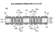
図2は、従来の配線基板の問題点を説明するための図である。図2において、図1に示す半導体装置200と同一構成部分には同一符号を付す。 FIG. 2 is a diagram for explaining the problems of the conventional wiring board. 2, the same components as those of the
しかしながら、シリコン基板、GaAs等の化合物半導体基板、ガラス基板(石英ガラス基板も含む)等の基板を基板本体211として用いた場合、基板本体211は樹脂基板と比較して破損しやすい。 However, when a substrate such as a silicon substrate, a compound semiconductor substrate such as GaAs, or a glass substrate (including a quartz glass substrate) is used as the
そのため、図2に示すように、配線基板201のハンドリング(例えば、配線基板201の完成後から配線基板201に電子部品202,203を実装するまでの間のハンドリング)により、基板本体211の角部又は外周部(角部も含む)が破損して、欠け部250が形成されてしまうという問題があった。 Therefore, as shown in FIG. 2, the corners of the
そこで本発明は、上述した問題点に鑑みなされたものであり、基板本体の角部又は外周部(角部も含む)の破損を防止することのできる配線基板及びその方法を提供することを目的とする。 Therefore, the present invention has been made in view of the above-described problems, and an object of the present invention is to provide a wiring board capable of preventing damage to corners or outer peripheral parts (including corners) of a board body and a method thereof. And
本発明の一観点によれば、基板本体と、前記基板本体を貫通する貫通電極と、前記基板本体の第1の面側に設けられ、前記貫通電極の一方の端部と電気的に接続されると共に、電子部品が実装されるパッドを有する第1の配線パターンと、前記第1の面とは反対側に位置する前記基板本体の第2の面側に設けられ、前記貫通電極の他方の端部と電気的に接続される外部接続用パッドを有する第2の配線パターンと、前記基板本体の前記第1の面側に、前記電子部品が実装されるパッドを露出する開口部を有すると共に、前記電子部品が実装されるパッド以外の部分の前記第1の配線パターンを覆う第1の絶縁樹脂層と、を備えた配線基板であって、前記第1の配線パターンを囲むように、前記第1の面側に位置する前記配線基板の角部に形成され、前記第1の面側に位置する前記基板本体の第1の角部および前記第1の絶縁樹脂層を切り欠く第1の切り欠き部と、前記第1の切り欠き部を覆う第1の樹脂とを設け、前記第1の樹脂は、前記第1の絶縁樹脂層の上部表面において暴露されており、前記配線基板の電子部品が実装される側の面が、前記第1の樹脂から露出していることを特徴とする配線基板が提供される。According to an aspect of the present invention, a substrate body, a through electrode penetrating the substrate body, a first surface side of the substrate body, and electrically connected to one end of the through electrode. And a first wiring pattern having a pad on which an electronic component is mounted, and a second surface side of the substrate body located on the opposite side of the first surface, A second wiring pattern having an external connection pad electrically connected to the end, andan opening for exposing the pad on which the electronic component is mounted on the first surface side of the substrate body; A first insulating resin layer that covers the first wiring pattern in a portion other than the pad on which the electronic component is mounted, and surrounds the first wiring pattern so as to surround the first wiring pattern. Formed at the corner of the wiring board located on the first surface side Is a first notch cut out first cornerand said first insulating resin layer of the substrate main body located on the first surface, the first covering the first notchThe first resin is exposed on the upper surface of the first insulating resin layer, and the surface of the wiring board on which the electronic component is mounted is formed from the first resin. A wiring board characterizedby being exposed is provided.
本発明によれば、第1の配線パターンを囲むように、基板本体の第1の面側に位置する配線基板の角部に形成され、基板本体の第1の面側に位置する基板本体の第1の角部を切り欠く第1の切り欠き部と、第1の切り欠き部を覆う第1の樹脂とを設けることで、破損しやすい基板本体の第1の角部を第1の樹脂で保護することが可能となる。これにより、配線基板のハンドリング(例えば、配線基板の完成後から配線基板に電子部品を実装するまでの間のハンドリング)により、基板本体の第1の角部が破損することを防止できる。 According to the present invention, the substrate body formed on the corner portion of the wiring board located on the first surface side of the board body so as to surround the first wiring pattern and located on the first surface side of the board body. By providing a first cutout portion that cuts out the first corner portion and a first resin that covers the first cutout portion, the first corner portion of the substrate main body that is easily damaged is provided as the first resin. It becomes possible to protect with. Thereby, it is possible to prevent the first corner portion of the board body from being damaged by the handling of the wiring board (for example, the handling after the completion of the wiring board until the electronic component is mounted on the wiring board).
また、前記第2の配線パターンを囲むように、前記第2の面側に位置する前記配線基板の角部に形成され、前記第2の面側に位置する前記基板本体の第2の角部を切り欠く第2の切り欠き部と、前記第2の切り欠き部を覆う第2の樹脂とを設けてもよい。 Further, a second corner portion of the substrate body is formed at a corner portion of the wiring board located on the second surface side so as to surround the second wiring pattern, and is located on the second surface side. A second cutout portion that cuts out the second cutout portion and a second resin that covers the second cutout portion may be provided.
これにより、破損しやすい基板本体の第2の角部を第2の樹脂で保護することが可能となるため、配線基板のハンドリング(例えば、配線基板の完成後から配線基板に電子部品を実装するまでの間のハンドリング)により、基板本体の第2の角部が破損することを防止できる。 This makes it possible to protect the second corner of the board main body that is easily damaged by the second resin, so that handling of the wiring board (for example, mounting an electronic component on the wiring board after completion of the wiring board) It is possible to prevent the second corner portion of the substrate body from being damaged by the handling up to).
また、前記第1の切り欠き部と前記第2の切り欠き部との間に位置する部分の前記基板本体の外周側面に、第3の樹脂を設けてもよい。 Moreover, you may provide 3rd resin in the outer peripheral side surface of the said board | substrate body of the part located between the said 1st notch part and the said 2nd notch part.
これにより、第1の切り欠き部と第2の切り欠き部との間に位置する部分の基板本体の外周側面を第3の樹脂で保護することが可能となるため、配線基板のハンドリング(例えば、配線基板の完成後から配線基板に電子部品を実装するまでの間のハンドリング)により、基板本体の外周側面が破損することを防止できる。 As a result, it becomes possible to protect the outer peripheral side surface of the substrate body at the portion located between the first cutout portion and the second cutout portion with the third resin. It is possible to prevent the outer peripheral side surface of the board body from being damaged by handling between the completion of the wiring board and the mounting of the electronic components on the wiring board.
本発明の他の観点によれば、基板本体と、前記基板本体を貫通する貫通電極と、前記基板本体の第1の面側に設けられ、前記貫通電極の一方の端部と電気的に接続されると共に、電子部品が実装されるパッドを有する第1の配線パターンと、前記第1の面とは反対側に位置する前記基板本体の第2の面側に設けられ、前記貫通電極の他方の端部と電気的に接続される外部接続用パッドを有する第2の配線パターンと、前記基板本体の前記第1の面側に、前記電子部品が実装されるパッドを露出する開口部を有すると共に、前記電子部品が実装されるパッド以外の部分の前記第1の配線パターンを覆う第1の絶縁樹脂層と、を備えた配線基板であって、前記配線基板の外周部に、前記第1及び第2の配線パターン及び前記貫通電極を囲むように形成され、前記配線基板の外周部に位置する部分の前記基板本体および前記第1の絶縁樹脂層を貫通する切り欠き部と、前記切り欠き部を覆う樹脂とを設け、前記樹脂は、前記第1の絶縁樹脂層の上部表面において暴露されており、前記配線基板の電子部品が実装される側の面が、前記樹脂から露出していることを特徴とする配線基板が提供される。According to another aspect of the present invention, the substrate body, the through electrode penetrating the substrate body, and the first surface side of the substrate body are electrically connected to one end of the through electrode. And a first wiring pattern having a pad on which an electronic component is mounted, and a second surface side of the substrate body located on the opposite side of the first surface, and the other of the through electrodes A second wiring pattern having an external connection pad electrically connected to an end of thesubstrate , andan opening exposing the pad on which the electronic component is mounted on the first surface side of the substrate body. And a first insulating resin layer that covers the first wiring pattern in a portion other than the pad on which the electronic component is mounted, wherein the first insulating resin layer covers the first wiring pattern on the outer periphery of the wiring substrate. And so as to surround the second wiring pattern and the through electrode Made, provided with notches extending through the substrate bodyand the first insulating resin layer in a portion located on an outer peripheral portion of the wiring substrate, and a resin covering saidnotches, said resin, said first There is provided a wiring board which is exposed on an upper surface of one insulating resin layer, and a surface of the wiring board on which an electronic component is mounted is exposed from the resin .
本発明によれば、配線基板の外周部に、第1及び第2の配線パターン及び貫通電極を囲むように形成され、配線基板の外周部に位置する部分の基板本体を貫通する切り欠き部と、切り欠き部を覆う樹脂とを設けたことにより、基板本体の外周部(角部も含む)を樹脂で保護することが可能となる。これにより、配線基板のハンドリング(例えば、配線基板の完成後から配線基板に電子部品を実装するまでの間のハンドリング)により、基板本体の外周部(角部も含む)が破損することを防止できる。 According to the present invention, the notch portion that is formed in the outer peripheral portion of the wiring board so as to surround the first and second wiring patterns and the through electrode and penetrates the portion of the substrate body located in the outer peripheral portion of the wiring substrate. By providing the resin that covers the notch, the outer peripheral portion (including the corner portion) of the substrate body can be protected with the resin. Thereby, it is possible to prevent the outer peripheral portion (including the corner portion) of the board body from being damaged by the handling of the wiring board (for example, the handling after the completion of the wiring board until the electronic component is mounted on the wiring board). .
本発明のその他の観点によれば、複数の配線基板形成領域と、前記複数の配線基板形成領域を囲むように配置された切断領域とを有した基板本体を準備する基板本体準備工程と、前記複数の配線基板形成領域に、前記基板本体を貫通する貫通電極と、前記貫通電極の一方の端部と電気的に接続されると共に、電子部品が実装されるパッドを有する第1の配線パターンと、前記貫通電極の他方の端部と電気的に接続される外部接続用パッドを有する第2の配線パターンと、を形成する貫通電極及び配線パターン形成工程と、前記電子部品が実装されるパッドを露出する開口部を有すると共に、前記電子部品が実装されるパッド以外の部分の前記第1の配線パターンを覆う第1の絶縁樹脂層を形成する絶縁樹脂層形成工程と、前記絶縁樹脂層形成工程後に、前記切断領域及び該切断領域と隣接する部分の前記複数の配線形成領域に対応する部分の前記第1の絶縁樹脂層及び前記基板本体に、前記切断領域の幅よりも幅広形状とされた第1の溝を形成する第1の溝形成工程と、前記第1の溝を充填し、前記第1の絶縁樹脂層上部表面において暴露される第1の樹脂を形成する第1の樹脂形成工程と、前記切断領域に対応する部分の前記基板本体、及び前記第1の溝に充填された前記第1の樹脂を切断して、前記複数の配線形成領域に形成された複数の前記配線基板を個片化する切断工程と、を含み、前記配線基板の電子部品が実装される側の面が、前記第1の樹脂から露出されていることを特徴とする配線基板の製造方法が提供される。According to another aspect of the present invention, a substrate body preparation step of preparing a substrate body having a plurality of wiring board formation regions and a cutting region disposed so as to surround the plurality of wiring substrate formation regions; A first wiring pattern having a plurality of wiring substrate forming regions, a through electrode penetrating the substrate body, a first wiring pattern electrically connected to one end portion of the through electrode and a pad on which an electronic component is mounted; A second wiring pattern having an external connection pad electrically connected to the other end of the through electrode, a through electrode and wiring pattern forming step, anda pad on which theelectronic component is mounted and having an opening exposing said a first insulating resin layer forming step of formingan insulating resinlayeron which an electronic component to cover the first wiring pattern in the portion other than the padsto bemounted, the insulating resin layer formed After that, the first insulating resin layer and the substrate body corresponding to the plurality of wiring forming regions in the cutting region and the portion adjacent to the cutting region are formed in a shape wider than the width of the cutting region. A first groove forming step for forming the first groove,and a first resin formation for filling the first groove and forming the first resinexposed on the upper surface of the first insulating resin layer process and the substrate body of the portion corresponding to the cuttingarea, and cutting the first resin filled in及 beauty said first groove, a plurality of the wiring formed in the plurality of wiring formation regionseen includingswitching and cross processthat turn into individual pieces of the substrate,a surface on which the electronic components of the circuit board is mounted is, the manufacturing method of a wiring substrate, characterized inthat it is exposed from the first resin Is provided.
本発明によれば、絶縁樹脂層形成工程後に、切断領域及び切断領域と隣接する部分の複数の配線形成領域に対応する部分の第1の絶縁樹脂層及び前記基板本体に、切断領域の幅よりも幅広形状とされた第1の溝を形成し、次いで、第1の溝を充填する第1の樹脂を形成し、次いで、切断領域に対応する部分の基板本体、及び第1の溝に充填された第1の樹脂を切断して、複数の配線形成領域に形成された複数の配線基板を個片化することで、第1の絶縁樹脂層が形成された側に位置する配線基板の角部に、第1の配線パターンを囲むように、基板本体の第1の角部を切り欠く第1の切り欠き部を形成すると共に、第1の切り欠き部を覆う第1の樹脂を形成することにより、配線基板のハンドリング(例えば、配線基板の完成後から配線基板に電子部品を実装するまでの間のハンドリング)により、基板本体の第1の角部が破損することを防止できる。According to the present invention, after the insulating resin layer forming step, the first insulating resin layer in the portion corresponding to the plurality of wiring forming regions adjacent to the cutting region and the cutting region, and the substrate body, the width of the cutting region forming a first groove which is also wider shape, then, the first resin filling the first groove is formed, and then, the substrate body of the portion corresponding to the cuttingregion, the first groove及 beauty By cutting the filled first resin and separating the plurality of wiring boards formed in the plurality of wiring forming regions, the wiring board positioned on the side on which the first insulating resin layer is formed is separated. In the corner portion, a first cutout portion that cuts out the first corner portion of the substrate body is formed so as to surround the first wiring pattern, and a first resin that covers the first cutout portion is formed. By handling the wiring board (for example, after the wiring board is completed, By the handling) of until implementing electronic component, it is possible to prevent the first corner of the substrate body may be damaged.
また、前記絶縁樹脂層形成工程においてさらに、前記外部接続用パッドを露出する開口部を有すると共に、前記外部接続用パッド以外の部分の前記第2の配線パターンを覆う第2の絶縁樹脂層を形成し、
前記第1の樹脂形成工程と前記切断工程との間に、前記切断領域及び該切断領域と隣接する部分の前記複数の配線形成領域に対応する部分の前記第2の絶縁樹脂層及び前記基板本体に、前記切断領域の幅よりも幅広形状とされた第2の溝を形成する第2の溝形成工程と、前記第2の溝を充填する第2の樹脂を形成する第2の樹脂形成工程と、を設け、前記切断工程では、前記切断領域に対応する部分の前記第1及び第2の樹脂及び前記基板本体を切断してもよい。Further, in the insulating resin layer forming step, a second insulating resin layer having an opening exposing the external connection pad and covering the second wiring pattern in a portion other than the external connection pad is formed. And
Between the first resin forming step and the cutting step, the second insulating resin layer and the substrate body in the portion corresponding to the plurality of wiring forming regions in the cutting region and a portion adjacent to the cutting region In addition, a second groove forming step of forming a second groove having a shape wider than the width of the cutting region, and a second resin forming step of forming a second resin filling the second groove If the provided wherein in cutting step, the first and second resin and the substrate body of the portion corresponding to the cutting region maybe disconnected.
これにより、配線基板のハンドリング(例えば、配線基板の完成後から配線基板に電子部品を実装するまでの間のハンドリング)により、基板本体の第2の角部が破損することを防止できる。 Thereby, it is possible to prevent the second corner portion of the board body from being damaged by handling the wiring board (for example, handling from the completion of the wiring board to mounting the electronic component on the wiring board).
本発明のその他の観点によれば、複数の配線基板形成領域と、前記複数の配線基板形成領域を囲むように配置された切断領域とを有した基板本体を準備する基板本体準備工程と、前記複数の配線基板形成領域に、前記基板本体を貫通する貫通電極と、前記貫通電極の一方の端部と電気的に接続されると共に、電子部品が実装されるパッドを有する第1の配線パターンと、前記貫通電極の他方の端部と電気的に接続される外部接続用パッドを有する第2の配線パターンと、を形成するパターン形成工程と、前記電子部品が実装されるパッドを露出する開口部を有すると共に、前記電子部品が実装されるパッド以外の部分の前記第1の配線パターンを覆う第1の絶縁樹脂層を形成する絶縁樹脂層形成工程と、前記絶縁樹脂層形成工程後に、前記切断領域及び該切断領域と隣接する部分の前記複数の配線形成領域を貫通すると共に、前記切断領域の幅よりも幅広形状とされた貫通溝を形成する貫通溝形成工程と、前記貫通溝を充填し、前記第1の絶縁樹脂層の上部表面において暴露される樹脂を形成する樹脂形成工程と、前記切断領域に対応する部分の前記樹脂を切断して複数の前記配線基板を個片化する切断工程と、を含み、前記配線基板の電子部品が実装される側の面が前記樹脂から露出されていることを特徴とする配線基板の製造方法が提供される。According to another aspect of the present invention, a substrate body preparation step of preparing a substrate body having a plurality of wiring board formation regions and a cutting region disposed so as to surround the plurality of wiring substrate formation regions; A first wiring pattern having a plurality of wiring substrate forming regions, a through electrode penetrating the substrate body, a first wiring pattern electrically connected to one end portion of the through electrode and a pad on which an electronic component is mounted; A pattern forming step of forming a second wiring pattern having an external connection pad electrically connected to the other end of the through electrode, and an opening exposing the pad on which theelectronic component is mounted and having a, the a first insulating resin layer forming step of formingan insulating resinlayeron which an electronic component to cover the first wiring pattern in the portion other than the padsto bemounted, after the insulating resin layer forming step, the switching Together through the plurality of wiring formation region of the part adjacent to the region and the cutting area, and the through groove forming step of forming a through groove which is wider shape than the width of the cutting region, filling the through groovethe first resin forming step of forming aexposed Ru resinin the upper surface of the insulating resin layer,disconnect the plurality of the wiring board by cutting the resin in a portion corresponding to the cutting regionthat turn into pieces A method of manufacturing a wiring board,wherein a surface of the wiring board on which an electronic component is mounted is exposed from the resin .
本発明によれば、絶縁樹脂層形成工程後に、切断領域及び切断領域と隣接する部分の複数の配線形成領域を貫通すると共に、切断領域の幅よりも幅広形状とされた貫通溝を形成し、次いで、貫通溝を充填する樹脂を形成し、次いで、切断領域に対応する部分の樹脂を切断して複数の前記配線基板を個片化することにより、第1及び第2の配線パターン及び貫通電極を囲むように配線基板の外周部に形成されると共に、樹脂に覆われた切り欠き部を形成することで、基板本体の外周部(角部も含む)を樹脂で保護することが可能となる。これにより、配線基板のハンドリング(例えば、配線基板の完成後から配線基板に電子部品を実装するまでの間のハンドリング)により、基板本体の外周部(角部も含む)が破損することを防止できる。 According to the present invention, after the insulating resin layer forming step, the cutting region and a plurality of wiring forming regions adjacent to the cutting region are penetrated, and a through groove having a shape wider than the width of the cutting region is formed, Next, a resin filling the through-groove is formed, and then the first and second wiring patterns and the through-electrodes are formed by cutting a portion of the resin corresponding to the cutting region and separating the plurality of wiring boards into pieces. By forming the cutout portion covered with the resin, the outer peripheral portion (including the corner portion) of the substrate body can be protected with the resin. . Thereby, it is possible to prevent the outer peripheral portion (including the corner portion) of the board body from being damaged by the handling of the wiring board (for example, the handling after the completion of the wiring board until the electronic component is mounted on the wiring board). .
本発明によれば、配線基板に設けられた基板本体の角部又は外周部(角部も含む)の破損を防止することができる。 According to the present invention, it is possible to prevent breakage of corner portions or outer peripheral portions (including corner portions) of a substrate body provided on a wiring board.
以下、図面に基づいて本発明の実施の形態について説明する。 Hereinafter, embodiments of the present invention will be described with reference to the drawings.
(第1の実施の形態)
図3は、本発明の第1の実施の形態に係る半導体装置の断面図である。(First embodiment)
FIG. 3 is a cross-sectional view of the semiconductor device according to the first embodiment of the present invention.
図3を参照するに、第1の実施の形態の半導体装置10は、配線基板11と、電子部品12,13と、外部接続端子15,16とを有する。 Referring to FIG. 3, the
配線基板11は、基板本体21と、絶縁膜22と、貫通電極23,24と、第1の配線パターン26,27と、配線パターン28と、第2の配線パターン31,32と、第1の絶縁樹脂層35と、第2の絶縁樹脂層36と、第1の切り欠き部である切り欠き部38と、第1の樹脂である樹脂39とを有する。 The
基板本体21は、板状とされており、貫通孔43,44を有する。基板本体21としては、例えば、シリコン基板、GaAs等の化合物半導体基板、ガラス基板(石英ガラス基板も含む)等を用いることができる。基板本体21としてシリコン基板を用いた場合、基板本体21の厚さは、例えば、200μmとすることができる。なお、本実施の形態では、基板本体21としてシリコン基板を用いた場合を例に挙げて以下の説明を行う。 The
絶縁膜22は、基板本体21の上面21A(第1の面)及び下面21B(第2の面)と、貫通孔43,44の側面に対応する部分の基板本体21の面とを覆うように形成されている。絶縁膜22としては、例えば、熱酸化膜や酸化膜(例えば、CVD法により形成された酸化膜)等を用いることができる。具体的には、絶縁膜22としては、例えば、SiO2膜を用いることができる。絶縁膜22として熱酸化膜又は酸化膜を用いた場合、絶縁膜22の厚さは、例えば、1μmとすることができる。The insulating
貫通電極23は、絶縁膜22が形成された貫通孔43に設けられている。貫通電極24は、絶縁膜22が形成された貫通孔44に設けられている。貫通電極23,24は、例えば、めっき法により形成することができる。貫通電極23,24の材料としては、例えば、Cuを用いることができる。 The through
第1の配線パターン26は、基板本体21の上面21Aに形成された絶縁膜22上に設けられている。第1の配線パターン26は、貫通電極23の上端と接続されている。第1の配線パターン26は、電子部品13が実装されるパッド46を有する。 The
第1の配線パターン27は、基板本体21の上面21Aに形成された絶縁膜22上に設けられている。第1の配線パターン27は、貫通電極24の上端と接続されている。第1の配線パターン27は、電子部品12が実装されるパッド47を有する。 The
配線パターン28は、電子部品12と電子部品13との間に位置する部分の絶縁膜22上に設けられている。配線パターン28は、一方の端部がパッド46と接続されており、他方の端部がパッド47と接続されている。 The
上記構成とされた第1の配線パターン26,27及び配線パターン28は、例えば、セミアディティブ法により形成することができる。また、第1の配線パターン26,27及び配線パターン28の材料としては、例えば、Cuを用いることができる。 The
第2の配線パターン31は、基板本体21の下面21Bに形成された絶縁膜22の下面に設けられている。第2の配線パターン31は、貫通電極23の下端と接続されている。これにより、第2の配線パターン31は、貫通電極23を介して、第1の配線パターン26と電気的に接続されている。第2の配線パターン31は、外部接続端子15が配設される外部接続用パッド51を有する。 The
第2の配線パターン32は、基板本体21の下面21Bに形成された絶縁膜22の下面に設けられている。第2の配線パターン32は、貫通電極24の下端と接続されている。これにより、第2の配線パターン32は、貫通電極24を介して、第1の配線パターン27と電気的に接続されている。第2の配線パターン32は、外部接続端子16が配設される外部接続用パッド52を有する。 The
上記構成とされた第2の配線パターン31,32は、例えば、セミアディティブ法により形成することができる。また、第2の配線パターン31,32の材料としては、例えば、Cuを用いることができる。 The
第1の絶縁樹脂層35は、パッド46,47を除いた部分の第1の配線パターン26,27及び配線パターン28を覆うように、絶縁膜22上に設けられている。第1の絶縁樹脂層35は、パッド46を露出する開口部35Aと、パッド47を露出する開口部35Bとを有する。第1の絶縁樹脂層35としては、例えば、ソルダーレジスト層を用いることができる。 The first insulating
第2の絶縁樹脂層36は、パッド51,52を除いた部分の第2の配線パターン31,32を覆うように、基板本体21の下面21Bに形成された絶縁膜22の下面に設けられている。第2の絶縁樹脂層36は、パッド51を露出する開口部36Aと、パッド52を露出する開口部36Bとを有する。第2の絶縁樹脂層35としては、例えば、ソルダーレジスト層を用いることができる。 The second insulating
切り欠き部38は、基板本体21の上面21A側に位置する配線基板11の角部に設けられている。切り欠き部38は、上面21A側に位置する基板本体21の角部(第1の角部)、及び基板本体21の角部の近傍に位置する絶縁膜22及び第1の絶縁樹脂層35に形成されている。切り欠き部38は、上面21A側に位置する基板本体21の角部、及び基板本体21の角部の近傍に位置する絶縁膜22及び第1の絶縁樹脂層35を切り欠くように構成されている。 The
切り欠き部38は、第1の配線パターン26,27及び配線パターン28を囲む平面視額縁形状とされている。基板本体21に形成された部分の切り欠き部38は、基板本体21の上面21Aから基板本体21の下面21Bに向かうにつれて幅が狭まる形状とされている。つまり、切り欠き部38の下端部は、先鋭形状とされている。先鋭形状とされていない部分の切り欠き部38の幅Jは、例えば、30μmとすることができる。 The
切り欠き部38は、例えば、ダイサーやレーザ加工により形成することができる。切り欠き部38をダイサーで加工する場合、ダイシングブレードは、例えば、その先端が先鋭形状とされたものを用いることができる。 The
樹脂39は、切り欠き部38を覆うように設けられている。樹脂39は、切り欠き部38と略等しい形状とされている。樹脂39の上部は、第1の絶縁樹脂層35の上面から突出している。樹脂39は、切り欠き部38に露出された部分の基板本体21(具体的には、上面21A側に位置する基板本体21の角部)を保護するためのものである。 The
このように、第1の配線パターン26,27を囲むように、基板本体21の上面21A側に位置する配線基板11の角部に形成され、基板本体21の角部を切り欠く切り欠き部38と、切り欠き部38を覆う樹脂39とを設けることにより、破損しやすい基板本体21の角部を樹脂39で保護することが可能となる。これにより、配線基板11のハンドリング(例えば、配線基板11の完成後から配線基板11に電子部品12,13を実装するまでの間のハンドリング)により、基板本体21の上面21A側に位置する基板本体21の角部が破損することを防止できる。 As described above, the
樹脂39としては、例えば、エポキシ樹脂、ポリイミド樹脂、シリコーン樹脂等を用いることができる。また、樹脂39の側面39Aは、基板本体21の外周側面21Cと略面一とされている。 As the
このように、樹脂39の側面39Aと基板本体21の外周側面21Cとが略面一となるように、切り欠き部38に樹脂39を設けることにより、配線基板11の面方向のサイズが大型化することを防止できる。 Thus, by providing the
電子部品12は、配線基板11に設けられたパッド47にフリップチップ実装されている。電子部品12と配線基板11との隙間には、アンダーフィル樹脂54が充填されている。電子部品13は、配線基板11に設けられたパッド46にフリップチップ実装されている。電子部品13は、配線パターン28を介して、電子部品12と電気的に接続されている。電子部品13と配線基板11との隙間には、アンダーフィル樹脂55が充填されている。電子部品12,13としては、例えば、半導体チップを用いることができる。 The
外部接続端子15は、外部接続用パッド51に設けられている。外部接続端子16は、外部接続用パッド52に設けられている。外部接続端子15,16は、半導体装置10をマザーボード等の実装基板(図示せず)に実装する際、実装基板に設けられたパッド(図示せず)と電気的に接続される端子である。 The
本実施の形態の配線基板によれば、第1の配線パターン26,27を囲むように、基板本体21の上面21A側に位置する配線基板11の角部に形成され、基板本体21の角部を切り欠く切り欠き部38と、切り欠き部38を覆う樹脂39とを設けることにより、破損しやすい基板本体21の角部を樹脂39で保護することが可能となる。これにより、配線基板11のハンドリング(例えば、配線基板11の完成後から配線基板11に電子部品12,13を実装するまでの間のハンドリング)により、基板本体21の上面21A側に位置する基板本体21の角部が破損することを防止できる。 According to the wiring board of the present embodiment, the corners of the
また、樹脂39の側面39Aと基板本体21の外周側面21Cとを略面一とすることで、配線基板11の面方向のサイズが大型化することを防止できる。 Further, by making the
なお、基板本体21としてガラス基板を用いた場合、GaAs基板やガラス基板は絶縁体であるため、上記説明した絶縁膜22が不要となる。 When a glass substrate is used as the
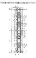
図4〜図12は、本発明の第1の実施の形態に係る配線基板の製造工程を示す図であり、図13は、図4に示す構造体の平面図である。図4〜図12において、第1の実施の形態の配線基板11と同一構成部分には同一符号を付す。また、図13において、図4に示す構造体と同一構成部分には、同一符号を付す。 4 to 12 are views showing a manufacturing process of the wiring board according to the first embodiment of the present invention, and FIG. 13 is a plan view of the structure shown in FIG. 4-12, the same code | symbol is attached | subjected to the same component as the
図4〜図13を参照して、第1の実施の形態の配線基板11の製造方法について説明する。始めに、図4に示す工程では、複数の配線基板形成領域Aと、複数の配線基板形成領域Aを囲むように配置された切断領域Bとを有した基板本体61を準備する(基板本体準備工程)。 With reference to FIGS. 4 to 13, a method for manufacturing the
配線基板形成領域Aは、配線基板11が形成される領域である。切断領域Bは、後述する図11に示す工程において、基板本体61が切断される領域である。基板本体61は、図11に示す工程において切断される(例えば、矩形に切断される)ことにより、複数の基板本体21(配線基板11の構成要素の1つ)となるものである。基板本体21としては、例えば、シリコン基板、GaAs等の化合物半導体基板、ガラス基板(石英ガラス基板も含む)等を用いることができる。なお、本実施の形態では、基板本体21としてシリコン基板を用いた場合を例に挙げて、以下の説明を行う。基板本体61としてシリコン基板を用いた場合、基板本体61の厚さは、例えば、200μmとすることができる。 The wiring board formation area A is an area where the
次いで、図5に示す工程では、周知の手法により、図4に示す複数の配線基板形成領域Aに貫通孔43,44を形成し、次いで、基板本体61の両面61A,61B及び貫通孔43,44に対応する部分の基板本体61の面を覆う絶縁膜22を形成し、次いで、貫通孔43,44に貫通電極23,24を形成し、その後、第1の配線パターン26,27、配線パターン28、及び第2の配線パターン31,32を形成する(貫通電極及び配線パターン形成工程)。 Next, in the process shown in FIG. 5, through
具体的には、貫通孔43,44は、例えば、エッチング法やレーザ加工法等の方法により形成する。なお、基板本体61として、ガラス基板を用いた場合、貫通孔43,44は、例えば、ウエットエッチング、サンドブラスト、機械加工等の方法により形成する。また、基板本体61としてガラス基板を用いた場合、絶縁膜22は不要となる。 Specifically, the through
絶縁膜22としては、例えば、熱酸化膜や酸化膜等を用いることができる。この場合、絶縁膜22は、例えば、熱酸化法やCVD法等の方法により形成することができる。貫通電極23,24、第1の配線パターン26,27、配線パターン28、及び第2の配線パターン31,32は、例えば、セミアディティブ法により形成することができる。貫通電極23,24、第1の配線パターン26,27、配線パターン28、及び第2の配線パターン31,32の材料としては、例えば、Cuを用いることができる。 For example, a thermal oxide film or an oxide film can be used as the insulating
次いで、図6に示す工程では、周知の手法により、基板本体61の上面61Aに形成された絶縁膜22に、パッド46,47を露出する開口部35A,35Bを有した第1の絶縁樹脂層35を形成すると共に、基板本体61の下面61Bに形成された絶縁膜22に、パッド51,52を露出する開口部36A,36Bを有した第2の絶縁樹脂層36を形成する(絶縁樹脂層形成工程)。第1及び第2の絶縁樹脂層35,36としては、例えば、ソルダーレジスト層を用いることができる。 Next, in the step shown in FIG. 6, a first insulating resin
次いで、図7に示す工程では、図6に示す構造体の下面側(第2の絶縁樹脂層36が形成されている側)にダイシングテープ64を貼り付ける。ダイシングテープ64の厚さは、例えば、300μmとすることができる。 Next, in the step shown in FIG. 7, a dicing
次いで、図8に示す工程では、切断領域B及び切断領域Bと隣接する部分の複数の配線形成領域Aに対応する部分の第1の絶縁樹脂層35、絶縁膜22、及び基板本体61に、切断領域Bの幅よりも幅広形状とされた溝66(第1の溝)を形成する(第1の溝形成工程)。 Next, in the step shown in FIG. 8, the first insulating
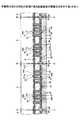
このとき、溝66は、切断領域Bの中心線Cを基準として左右対称となるように形成するとよい。溝66は、例えば、ダイサーやレーザ加工により形成することができる。ダイサーを用いて溝66を形成する場合、ダイシングブレードは、例えば、その先端が先鋭形状とされたものを用いることができる。 At this time, the
溝66は、後述する図11に示す工程で切断されることにより、図3で説明した切り欠き部38(配線基板11の構成要素の1つ)となる溝である。切断領域Bの幅が40μmの場合、溝66の幅Dは、例えば、100μmとすることができる。この場合、溝66の深さは、例えば、100μmとすることができる。 The
次いで、図9に示す工程では、第1の絶縁樹脂層35上に、溝66と対向する部分に貫通溝67Aを有したステンシルマスク67を載置し、その後、印刷法により、溝66を充填する樹脂39(第1の樹脂)を形成する(第1の樹脂形成工程)。 Next, in the step shown in FIG. 9, a
このとき、貫通溝67Aにも樹脂39が形成される。図9に示す樹脂39は、先に説明した図3に示す樹脂39の母材である。樹脂39としては、例えば、エポキシ樹脂、ポリイミド樹脂、シリコーン樹脂等を用いることができる。なお、この段階では、樹脂39は、完全には硬化していない(つまり、樹脂39は半硬化状態である。)。貫通溝67Aの幅は、溝66の幅と略等しくなるように構成されている。溝66の幅が100μmの場合、貫通溝67Aの幅は、例えば、100μmとすることができる。ステンシルマスク67の厚さは、例えば、30μmとすることができる。 At this time, the
次いで、図10に示す工程では、図9に示すステンシルマスク67を除去した後、図9に示す半硬化状態の樹脂39を完全に硬化させる。樹脂69が熱硬化性のエポキシ樹脂の場合、例えば、半硬化状態の樹脂39を160℃に加熱することで樹脂39を完全に硬化させる。完全に硬化した樹脂39は、後述する図11に示す工程で切断されることにより、図3に示す樹脂39(配線基板11の構成要素の1つ)となる。 Next, in the step shown in FIG. 10, after removing the
次いで、図11に示す工程では、図10に示す構造体のうち、切断領域Bに対応する部分の基板本体61、絶縁膜22、第2の絶縁樹脂層36、及び樹脂39を切断することにより、複数の配線形成領域Aに形成された複数の配線基板11を個片化することで、第1の絶縁樹脂層35が形成された側に位置する配線基板11の角部に、第1の配線パターン26,27を囲むように、基板本体21の第1の角部を切り欠く切り欠き部38を形成すると共に、切り欠き部38を覆う樹脂39(完全に硬化した樹脂)を形成する(切断工程)。このとき、溝66の幅Dは、切断領域Bの幅Bよりも広いため、ダイシングテープ64上において、分離された複数の配線基板11に設けられた切り欠き部38には樹脂39が残る。切断領域Bに対応する部分の基板本体61、第2の絶縁樹脂層36、絶縁膜22、及び樹脂39の切断は、例えば、ダイサーやレーザ加工等の方法により行うことができる。なお、この段階では、複数の配線基板11は、個片化された状態でダイシングテープ64に接着されている。 Next, in the step shown in FIG. 11, by cutting the
次いで、図12に示す工程では、図11に示すダイシングテープ64を除去する。これにより、複数の配線基板11は、完全に分離される。 Next, in the step shown in FIG. 12, the dicing
本実施の形態の配線基板の製造方法によれば、絶縁樹脂層形成工程後に、切断領域B及び切断領域Bと隣接する部分の複数の配線形成領域Aに対応する部分の第1の絶縁樹脂層35、絶縁膜22、及び基板本体61に、切断領域Bの幅よりも幅広形状とされた溝66を形成し、次いで、溝66を充填する樹脂39を形成し、次いで、切断領域Bに対応する部分の基板本体61、第2の絶縁樹脂層36、及び溝66に充填された樹脂39を切断して、複数の配線形成領域Aに形成された複数の配線基板11を個片化することで、第1の絶縁樹脂層35が形成された側に位置する配線基板11の角部に、第1の配線パターン26,27を囲むように、基板本体21の角部を切り欠く切り欠き部38を形成すると共に、切り欠き部38を覆う樹脂39を形成することにより、配線基板11のハンドリング(例えば、配線基板11の完成後から配線基板11に電子部品12,13を実装するまでの間のハンドリング)により、上面21A側に位置する基板本体21の角部が破損することを防止できる。 According to the method for manufacturing a wiring substrate of the present embodiment, after the insulating resin layer forming step, the first insulating resin layer in the portion corresponding to the cutting region B and the plurality of wiring forming regions A in the portion adjacent to the cutting region B. 35, the insulating
図14は、本発明の第1の実施の形態の変形例に係る配線基板の製造工程を示す図である。図14において、先に説明した図9に示す構造体と同一構成部分には同一符号を付す。 FIG. 14 is a diagram showing a manufacturing process of the wiring board according to the modification of the first embodiment of the present invention. In FIG. 14, the same components as those of the structure shown in FIG.
なお、本実施の形態では、貫通溝67Aを有したマスク67を用いた印刷法により溝66に樹脂39を充填する場合(図9参照)を例に挙げて説明したが、マスク67を用いた印刷法の代わりに、図14に示すように、インクジェット法やディスペンス法により、溝66を充填する樹脂39を形成してもよい。この場合、マスク67が不要となると共に、配線基板11に設けられた樹脂39の上面と第1の絶縁樹脂層35の上面とを略面一にすることが可能となる。 In the present embodiment, the case where the
図15は、本発明の第1の実施の形態の第1変形例に係る半導体装置の断面図である。図15において、第1の実施の形態の半導体装置10と同一構成部分には、同一符号を付す。 FIG. 15 is a cross-sectional view of a semiconductor device according to a first variation of the first embodiment of the present invention. In FIG. 15, the same components as those of the
図15を参照するに、第1の実施の形態の第1変形例に係る半導体装置75は、第1の実施の形態の半導体装置10に設けられた配線基板11の代わりに、配線基板76を設けた以外は、半導体装置10と同様に構成される。 Referring to FIG. 15, a
配線基板76は、配線基板11に設けられた切り欠き部38及び樹脂39の代わりに、切り欠き部77及び樹脂78を設けた以外は、配線基板11と同様に構成される。 The
切り欠き部77は、切り欠き部77の下端部の断面形状が四角形とされていること以外は、切り欠き部38と同様な構成とされている。切り欠き部77は、例えば、刃幅が略一定とされ、先端が平坦な形状とされたダイシングブレードを用いて、第1の絶縁樹脂層35、絶縁膜22、及び基板本体21の一部を切断することで形成できる。 The
樹脂78は、切り欠き部77に設けられている。樹脂78は、樹脂78の下端部の断面形状が四角形とされていること以外は、樹脂39と同様な構成とされている。樹脂78の側面78Aは、基板本体21の外周側面21Cと略面一とされている。樹脂78の上端は、第1の絶縁樹脂層35の上面から上方へ突出している。 The
このような構成とされた第1の実施の形態の第1変形例の配線基板76は、第1の実施の形態の配線基板11と同様な効果を得ることができる。なお、図15では、樹脂78の上端が第1の絶縁樹脂層35の上面から突出した場合を例に挙げて説明したが、樹脂78の上端面と第1の絶縁樹脂層35の上面とを略面一にしてもよい。 The
また、第1の実施の形態の第1変形例の配線基板76は、切断されることで切り欠き部77となる溝を形成する際、刃幅が略一定とされ、先端が平坦な形状とされたダイシングブレードを用いること以外は、第1の実施の形態の配線基板11の製造方法と同様な手法により形成することができ、第1の実施の形態の配線基板11の製造方法と同様な効果を得ることができる。 Further, the
図16は、本発明の第1の実施の形態の第2変形例に係る半導体装置の断面図である。図16において、第1の実施の形態の半導体装置10と同一構成部分には、同一符号を付す。 FIG. 16 is a cross-sectional view of a semiconductor device according to a second modification of the first embodiment of the present invention. In FIG. 16, the same components as those of the
図16を参照するに、第1の実施の形態の第2変形例に係る半導体装置85は、第1の実施の形態の半導体装置10に設けられた配線基板11の代わりに、配線基板86を設けた以外は、半導体装置10と同様に構成される。 Referring to FIG. 16, a
配線基板86は、配線基板11に設けられた切り欠き部38及び樹脂39の代わりに、切り欠き部88及び樹脂89を設けた以外は、配線基板11と同様に構成される。 The
切り欠き部88は、配線基板11に設けられた切り欠き部38を上下反転させた形状とされており、第2の絶縁樹脂層36が形成された側の配線基板86の角部に設けられている。切り欠き部88は、第2の配線パターン31,32を囲むように配置されている。 The
樹脂89は、配線基板11に設けられた樹脂39を上下反転させた形状とされており、切り欠き部88を覆うように設けられている。樹脂89の側面89Aは、基板本体21の外周側面21Cと略面一とされている。樹脂89の下端は、第2の絶縁樹脂層36の下面から下方へ突出している。樹脂89としては、例えば、エポキシ樹脂、ポリイミド樹脂、シリコーン樹脂等を用いることができる。 The
このような構成とされた第1の実施の形態の第2変形例の配線基板86は、第1の実施の形態の配線基板11と同様な効果を得ることができる。なお、図16では、樹脂89の下端が第2の絶縁樹脂層36の下面から突出した場合を例に挙げて説明したが、樹脂89の下端面と第2の絶縁樹脂層36の下面とを略面一にしてもよい。 The
また、第1の実施の形態の第2変形例に係る配線基板86は、第1の実施の形態の配線基板11の製造方法を同様な手法により形成することができ、第1の実施の形態の配線基板11の製造方法と同様な効果を得ることができる。 In addition, the
(第2の実施の形態)
図17は、本発明の第2の実施の形態に係る半導体装置の断面図である。図17において、第1の実施の形態の半導体装置10と同一構成部分には同一符号を付す。(Second Embodiment)
FIG. 17 is a cross-sectional view of a semiconductor device according to the second embodiment of the present invention. In FIG. 17, the same components as those of the
図17を参照するに、第2の実施の形態の半導体装置100は、第1の実施の形態の半導体装置に設けられた配線基板11の代わりに、配線基板101を設けた以外は、半導体装置10と同様に構成される。 Referring to FIG. 17, the
配線基板101は、配線基板11の構成に、さらに図16で説明した切り欠き部88(本実施の形態の場合、第2の切り欠き部)及び樹脂89(本実施の形態の場合、第2の樹脂)を設けた以外は、配線基板11と同様に構成される。 The
つまり、配線基板101では、配線基板101の上面側の外周部(配線基板101の角部も含む)が樹脂39に覆われると共に、配線基板101の下面側の外周部(配線基板101の角部も含む)が樹脂89で覆われている。これにより、配線基板101では、基板本体21の両面21A,21Bの角部(第1及び第2の角部)が樹脂39,89で覆われると共に、樹脂39,89から露出されている部分の基板本体21の外周側面21Cの面積を小さくすることが可能となる。 That is, in the
本実施の形態の配線基板によれば、第1の配線パターン26,27を囲むように、基板本体21の上面21A側に位置する配線基板11の角部に形成され、基板本体21の角部(第1の角部)を切り欠く切り欠き部38と、切り欠き部38を覆う樹脂39と、第2の配線パターン31,32を囲むように、基板本体21の下面21B側に位置する配線基板11の角部に形成され、基板本体21の角部(第2の角部)を切り欠く切り欠き部88と、切り欠き部88を覆う樹脂89と、を設けることにより、破損しやすい基板本体21の角部(第1及び第2の角部)が樹脂39,89で覆われると共に、樹脂39,89から露出されている部分の基板本体21の外周側面21Cの面積を小さくすることが可能となる。これにより、配線基板101のハンドリング(例えば、配線基板101の完成後から配線基板101に電子部品12,13を実装するまでの間のハンドリング)により、基板本体21の角部(第1及び第2の角部)及び樹脂39,89に覆われた部分の基板本体21の側壁が破損することを防止できる。 According to the wiring board of the present embodiment, the corners of the
なお、図17では、樹脂39の上端が第1の絶縁樹脂層35の上面から突出すると共に、樹脂89の下端が第2の絶縁樹脂層36の下面から突出した場合を例に挙げて説明したが、樹脂39の上端面と第1の絶縁樹脂層35の上面とを略面一にする共に、樹脂89の下端面と第2の絶縁樹脂層36の下面とが略面一となるように構成してもよい。 In FIG. 17, the case where the upper end of the
図18〜図23は、本発明の第2の実施の形態に係る配線基板の製造工程を示す図である。図18〜図23において、先に説明した図10〜図12に示す構造体及び第2の実施の形態の配線基板101と同一構成部分には同一符号を付す。 18 to 23 are views showing manufacturing steps of the wiring board according to the second embodiment of the present invention. 18 to 23, the same reference numerals are given to the same components as those of the structure shown in FIGS. 10 to 12 described above and the
始めに、図4〜図10に示す工程と同様な処理を行うことで、図10に示す構造体を形成する。次いで、図18に示す工程では、図10に示す構造体からダイシングテープ64を除去し、次いで、ダイシングテープ106にダイシングテープ64が除去された構造体の上下を反転させた状態で貼り付ける。 First, the structure shown in FIG. 10 is formed by performing the same process as the steps shown in FIGS. Next, in the process shown in FIG. 18, the dicing
次いで、図19に示す工程では、第2の配線パターン31,32が形成された側から切断領域B及び切断領域Bと隣接する部分の複数の配線形成領域Aに対応する部分の第2の絶縁樹脂層36、絶縁膜22、及び基板本体61に、切断領域Bの幅よりも幅広形状とされた溝107(第2の溝)を形成する(第2の溝形成工程)。 Next, in the step shown in FIG. 19, the second insulation of the part corresponding to the plurality of wiring forming areas A adjacent to the cutting area B and the cutting area B from the side where the
このとき、溝107は、切断領域Bの中心線Cを基準として左右対称となるように形成する。また、溝107は、溝66と接続させてもよいし、溝66から少し離間させてもよい。溝107は、例えば、ダイサーやレーザ加工により形成することができる。ダイサーを用いて溝107を形成する際に使用するダイシングブレードは、例えば、その先端が先鋭形状とされたものを用いることができる。 At this time, the
溝107は、後述する図22に示す工程で切断されることにより、図17で説明した切り欠き部88(配線基板101の構成要素の1つ)となる溝である。切断領域Bの幅が40μmの場合、溝107の幅Eは、例えば、100μmとすることができる。この場合、溝107の深さは、例えば、100μmとすることができる。 The
次いで、図20に示す工程では、第2の絶縁樹脂層36上に、溝107と対向する部分に貫通溝67Aを有したステンシルマスク67を載置し、その後、印刷法により、溝107を充填する樹脂89(第2の樹脂)を形成する(第2の樹脂形成工程)。 Next, in the process shown in FIG. 20, a
このとき、貫通溝67Aにも樹脂89が形成される。図20に示す樹脂89は、先に説明した図17に示す樹脂89の母材である。樹脂89としては、例えば、エポキシ樹脂、ポリイミド樹脂、シリコーン樹脂等を用いることができる。なお、この段階では、樹脂89は、完全には硬化していない(つまり、樹脂89は半硬化状態である。)。貫通溝67Aの幅は、溝107の幅と略等しくなるように構成されている。溝107の幅が100μmの場合、貫通溝67Aの幅は、例えば、100μmとすることができる。ステンシルマスク67の厚さは、例えば、30μmとすることができる。 At this time, the
次いで、図21に示す工程では、図20に示すステンシルマスク67を除去した後、樹脂89を硬化させる。樹脂89が熱硬化性のエポキシ樹脂の場合、例えば、樹脂89を160℃に加熱することで樹脂89を硬化させる。硬化した樹脂89は、後述する図22に示す工程で切断されることにより、図17で説明した樹脂89(配線基板101の構成要素の1つ)となるものである。 Next, in the step shown in FIG. 21, after removing the
次いで、図22に示す工程では、図21に示す構造体のうち、切断領域Bに対応する部分の樹脂39,89及び基板本体61を切断することにより、複数の配線形成領域Aに形成された複数の配線基板101を個片化する(切断工程)。 Next, in the step shown in FIG. 22, the
これにより、第1の絶縁樹脂層35が形成された側に位置する配線基板101の角部に、樹脂39に覆われると共に、第1の配線パターン26,27を囲むように、第1の絶縁樹脂層35側に位置する基板本体21の角部を切り欠く切り欠き部38が形成されると共に、第2の絶縁樹脂層36が形成された側に位置する配線基板101の角部に、樹脂89に覆われると共に、第2の配線パターン31,32を囲むように、第2の絶縁樹脂層36側に位置する基板本体21の角部を切り欠く切り欠き部88が形成される。 As a result, the first insulating
このとき、溝66,107の幅D,Eは、切断領域Bの幅よりも広いため、ダイシングテープ106上において、分離された複数の配線基板101の第1の絶縁樹脂層35の上面側には樹脂39が残り、分離された複数の配線基板101の第2の絶縁樹脂層36の下面側には樹脂89が残る。 At this time, since the widths D and E of the
切断領域Bに対応する部分の基板本体61及び樹脂69,89の切断は、例えば、ダイサーやレーザ加工等の手法により行うことができる。なお、この段階では、個片化された複数の配線基板101は、ダイシングテープ106に接着されている。 The substrate
次いで、図23に示す工程では、図22に示すダイシングテープ106を除去する。これにより、複数の配線基板101は、完全に分離される。 Next, in the step shown in FIG. 23, the dicing
本実施の形態の配線基板の製造方法によれば、溝66に樹脂39を形成した後、第2の配線パターン31,32が形成された側から切断領域B及び切断領域Bと隣接する部分の複数の配線形成領域Aに対応する部分の第2の絶縁樹脂層36、絶縁膜22、及び基板本体61に、切断領域Bの幅よりも幅広形状とされた溝107(第2の溝)を形成し、次いで、溝107を充填する樹脂89を形成し、その後、切断領域Bに対応する部分の樹脂39,89及び基板本体61を切断して、複数の配線形成領域Aに形成された複数の配線基板101を個片化することにより、樹脂39に覆われ、第1の配線パターン26,27を囲むように、第1の絶縁樹脂層35側に位置する基板本体21の角部(第1の角部)を切り欠く切り欠き部38と、樹脂89に覆われ、第2の配線パターン31,32を囲むように、第2の絶縁樹脂層36側に位置する基板本体21の角部を切り欠く切り欠き部88(第2の角部)とが形成されため、破損しやすい基板本体21の角部(第1及び第2の角部)が樹脂39,89で覆われると共に、樹脂39,89から露出されている部分の基板本体21の外周側面21Cの面積を小さくすることが可能となる。 According to the method for manufacturing a wiring board of the present embodiment, after forming the
これにより、配線基板101のハンドリング(例えば、配線基板101の完成後から配線基板101に電子部品12,13を実装するまでの間のハンドリング)により、基板本体21の角部(第1及び第2の角部)及び樹脂39,89に覆われた部分の基板本体21の側壁が破損することを防止できる。 Accordingly, the corners (first and second) of the
図24は、本発明の第2の実施の形態の第1変形例に係る半導体装置の断面図である。図24において、先に説明した第1の実施の形態の第1変形例に係る半導体装置75と同一構成部分には同一符号を付す。 FIG. 24 is a cross-sectional view of a semiconductor device according to a first modification of the second embodiment of the present invention. In FIG. 24, the same components as those of the
図24を参照して、第2の実施の形態の第1変形例に係る半導体装置115は、第1の実施の形態の第1変形例に係る半導体装置75に設けられた配線基板76の代わりに、配線基板116を設けた以外は半導体装置75と同様に構成される。 Referring to FIG. 24, a
配線基板116は、配線基板76の構成に、さらに、切り欠き部117(第2の切り欠き部)及び樹脂118(第2の樹脂)を設けた以外は、配線基板76と同様に構成される。切り欠き部117は、基板本体21の下面21B側に位置する配線基板116の角部に設けられている。切り欠き部117は、切り欠き部77と同様な形状とされており、第2の配線パターン31,32を囲んでいる。 The
樹脂118は、切り欠き部117に設けられている。樹脂118は、樹脂78と同様な構成(同様な形状及び材料)とされている。樹脂118の下端は、第2の絶縁樹脂層36の下面から突出している。また、樹脂118の側面118Aと基板本体21の外周側面21Cとは、略面一とされている。 The
このような構成とされた第2の実施の形態の第1変形例に係る配線基板116は、第2の実施の形態の配線基板101と同様な効果を得ることができる。つまり、基板本体21の両面21A,21Bの角部に形成する切り欠き部の形状や樹脂の形状は、本実施の形態で説明した切り欠き部38,88,77,117の形状及び樹脂39,89,78,118の形状に限定されない。 The
なお、図24では、樹脂78の上端が第1の絶縁樹脂層35の上面から突出すると共に、樹脂118の下端が第2の絶縁樹脂層36の下面から突出した場合を例に挙げて説明したが、樹脂78の上端面と第1の絶縁樹脂層35の上面とを略面一にする共に、樹脂118の下端面と第2の絶縁樹脂層36の下面とが略面一となるように構成してもよい。 24, the case where the upper end of the
上記構成とされた配線基板116は、切断されることで切り欠き部38,88となる溝(図示せず)を形成する際、刃幅が略一定とされ、先端が平坦な形状とされたダイシングブレードを用いること以外は、第2の実施の形態の配線基板101の製造方法と同様な手法により製造することができる。 When the
図25は、本発明の第2の実施の形態の第2変形例に係る半導体装置の断面図である。図25において、第2の実施の形態の半導体装置100と同一構成部分には同一符号を付す。 FIG. 25 is a cross-sectional view of a semiconductor device according to a second modification of the second embodiment of the present invention. In FIG. 25, the same components as those of the
図25を参照するに、第2の実施の形態の第2変形例に係る半導体装置120は、第2の実施の形態の半導体装置100に設けられた配線基板101の代わりに、配線基板121を設けた以外は、半導体装置100と同様に構成される。 Referring to FIG. 25, a
配線基板121は、配線基板101の構成に、さらに樹脂123(第3の樹脂)を設けた以外は配線基板101と同様に構成される。樹脂123は、樹脂39と樹脂89との間に位置する基板本体21の外周側面21Cを覆うように設けられている。樹脂123としては、例えば、エポキシ樹脂、ポリイミド樹脂、シリコーン樹脂等を用いることができる。樹脂123は、例えば、ディスペンス法により形成することができる。 The
このように、切り欠き部38,88と、切り欠き部38を覆う樹脂39と、切り欠き部88を覆う樹脂89と、樹脂39と樹脂89との間に位置する基板本体21の外周側面21Cを覆う樹脂123とを設けることで、樹脂39,89,123により基板本体21の両面21A,21Bに形成された角部(第1及び第2の角部)及び基板本体21の外周側面21Cを保護することが可能となる。 As described above, the
このため、配線基板121のハンドリング(例えば、配線基板121の完成から配線基板121に電子部品12,13を実装するまでの間のハンドリング)により、基板本体21の両面21A,21Bに形成された角部(第1及び第2の角部)及び基板本体21の外周側面21Cが破損することを防止できる。 Therefore, the corners formed on both
図26は、本発明の第2の実施の形態の第3変形に係る半導体装置の断面図である。図26において、第2の実施の形態の第1変形例に係る半導体装置115と同一構成部分には同一符号を付す。 FIG. 26 is a cross-sectional view of a semiconductor device according to a third variation of the second embodiment of the present invention. In FIG. 26, the same components as those of the
図26を参照するに、第2の実施の形態の第3変形例に係る半導体装置125は、第2の実施の形態の第1変形例に係る配線基板115に設けられた配線基板116の代わりに、配線基板126を設けた以外は、配線基板115と同様に構成される。 Referring to FIG. 26, the
配線基板126は、配線基板115の構成に、さらに樹脂128を設けた以外は、配線基板115と同様な構成とされている。樹脂128は、樹脂78と樹脂118との間に位置する部分の基板本体21の外周側面21Cを覆うように設けられている。樹脂123としては、例えば、エポキシ樹脂、ポリイミド樹脂、シリコーン樹脂等を用いることができる。樹脂123は、例えば、ディスペンス法により形成することができる。 The
上記構成とされた第2の実施の形態の第3変形例に係る配線基板126は、第2の実施の形態の第2変形例に係る配線基板121と同様な効果を得ることができる。 The
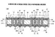
(第3の実施の形態)
図27は、本発明の第3の実施の形態に係る半導体装置の断面図である。図27において、第1の実施の形態の半導体装置10と同一構成部分には同一符号を付す。(Third embodiment)
FIG. 27 is a sectional view of a semiconductor device according to the third embodiment of the present invention. In FIG. 27, the same components as those of the
図27を参照するに、第3の実施の形態の半導体装置130は、第1の実施の形態の半導体装置10に設けられた配線基板11の代わりに、配線基板131を設けた以外は、半導体装置10と同様に構成される。 Referring to FIG. 27, the
配線基板131は、配線基板11に設けられた切り欠き部38及び樹脂39の代わりに、切り欠き部133及び樹脂134を設けた以外は、配線基板11と同様に構成されている。 The
切り欠き部133は、連続する切り欠き部であり、配線基板131の外周部に設けられている。切り欠き部133は、配線基板131の外周部に位置する部分の基板本体21、絶縁膜22、第1の絶縁樹脂層35、及び第2の絶縁樹脂層36を貫通するように形成されている。切り欠き部133は、第1及び第2の配線パターン26,27,31、32と貫通電極23,24とを囲むような形状とされている。 The
樹脂134は、切り欠き部133を覆うように設けられている。樹脂134は、基板本体21の外周側面21D全体を覆っている。樹脂134としては、例えば、エポキシ樹脂、ポリイミド樹脂、シリコーン樹脂等を用いることができる。 The
本実施の形態の配線基板によれば、配線基板131の外周部に、第1及び第2の配線パターン26,27,31,32及び貫通電極23,24を囲むように形成され、配線基板131の外周部に位置する部分の基板本体21を貫通する切り欠き部133と、切り欠き部133を覆う樹脂134とを設けたことにより、基板本体21の外周部(基板本体21の両面21A,21Bに形成された角部も含む)を樹脂134で保護することが可能となる。これにより、配線基板131のハンドリング(例えば、配線基板131の完成後から配線基板131に電子部品12,13を実装するまでの間のハンドリング)により、基板本体21の外周部(基板本体21の両面21A,21Bに形成された角部も含む)が破損することを防止できる。 According to the wiring board of the present embodiment, the
図28〜図33は、本発明の第3の実施の形態に係る配線基板の製造工程を示す図である。図28〜図33において、図6に示す構造体及び第3の実施の形態の配線基板131と同一構成部分には同一符号を付す。 28 to 33 are views showing a manufacturing process of the wiring board according to the third embodiment of the present invention. 28 to 33, the same components as those of the structure shown in FIG. 6 and the
図28〜図33を参照して、第3の実施の形態の配線基板131の製造方法について説明する。始めに、第1の実施の形態で説明した図4〜図6に示す工程と同様な処理を行うことで、図6に示す構造体を形成する。 With reference to FIGS. 28 to 33, a method of manufacturing the
次いで、図28に示す工程では、ダイシングテープ64が接着された支持体141を準備し、図6に示す構造体をダイシングテープ64に接着させる。支持体141は、補強板の機能を有する部材である。支持体141としては、例えば、ガラス板を用いることができる。この場合、支持体141の厚さは、例えば、500μmとすることができる。 Next, in a step shown in FIG. 28, a support 141 to which the dicing
次いで、図29に示す工程では、切断領域B及び切断領域Bと隣接する部分の複数の配線形成領域Aに対応する部分の絶縁膜22、第1の絶縁樹脂層35、第2の絶縁樹脂層36、及び基板本体61に、絶縁膜22、第1の絶縁樹脂層35、第2の絶縁樹脂層36、及び基板本体61を貫通すると共に、切断領域Bの幅よりも幅広形状とされた貫通溝143を形成する(貫通溝形成工程)。 Next, in the step shown in FIG. 29, the insulating
このとき、貫通溝143は、切断領域Bの中心線Cを基準として左右対称となるように形成する。貫通溝143は、例えば、ダイサーやレーザ加工により形成することができる。貫通溝143は、後述する図32に示す工程において切断されることにより、図27で説明した切り欠き部133(配線基板131の構成要素の1つ)となる溝である。切断領域Bの幅が40μmの場合、貫通溝143の幅Fは、例えば、100μmとすることができる。 At this time, the through
次いで、図30に示す工程では、第2の絶縁樹脂層36上に、貫通溝143と対向する部分に貫通溝67Aを有したステンシルマスク67を載置し、その後、印刷法により、貫通溝143を充填する樹脂134を形成する(樹脂形成工程)。 Next, in the step shown in FIG. 30, a
このとき、貫通溝67Aにも樹脂134が形成される。図30に示す樹脂134は、先に説明した図27に示す樹脂134の母材である。樹脂134としては、例えば、エポキシ樹脂、ポリイミド樹脂、シリコーン樹脂等を用いることができる。なお、この段階では、樹脂134は、完全には硬化していない(つまり、樹脂134は半硬化状態である。)。貫通溝67Aの幅は、貫通溝143の幅と略等しくなるように構成されている。貫通溝143の幅が100μmの場合、貫通溝67Aの幅は、例えば、100μmとすることができる。ステンシルマスク67の厚さは、例えば、30μmとすることができる。 At this time, the
次いで、図31に示す工程では、図30に示すステンシルマスク67を除去した後、樹脂134を硬化させる。樹脂134が熱硬化性のエポキシ樹脂の場合、例えば、樹脂134を160℃に加熱することで樹脂134を硬化させる。硬化した樹脂134は、後述する図32に示す工程で切断されることにより、図27で説明した樹脂134(配線基板131の構成要素の1つ)となるものである。 Next, in the step shown in FIG. 31, after removing the
次いで、図32に示す工程では、図31に示す構造体のうち、切断領域Bに対応する部分の樹脂134を切断することにより、複数の配線形成領域Aに形成された複数の配線基板131を個片化する(切断工程)。 Next, in the step shown in FIG. 32, the plurality of
これにより、配線基板131の外周部に、第1及び第2の配線パターン26,27,31、32と貫通電極23,24とを囲む切り欠き部133と、切り欠き部133を覆う樹脂134とが形成される。 As a result, a
このとき、貫通溝の幅Fは、切断領域Bの幅よりも広いため、ダイシングテープ64上において、分離された複数の配線基板131に設けられた基板本体21の外周側面21D全体を樹脂134で覆うことが可能となる。これにより、配線基板131のハンドリング(例えば、配線基板131の完成後から配線基板131に電子部品12,13を実装するまでの間のハンドリング)により、基板本体21の外周部が破損することを防止できる。 At this time, since the width F of the through groove is wider than the width of the cutting region B, the entire outer
切断領域Bに対応する部分の樹脂134の切断は、例えば、ダイサーやレーザ加工等の方法により行うことができる。なお、この段階では、個片化された複数の配線基板131は、ダイシングテープ64に接着されている。 The cutting of the
次いで、図33に示す工程では、図32に示すダイシングテープ64及び支持体141を除去する。これにより、複数の配線基板131は、完全に分離される。 Next, in the step shown in FIG. 33, the dicing
本実施の形態の配線基板の製造方法によれば、貫通電極23,24、第1及び第2の配線パターン26,27,31,32、及び第1及び第2の絶縁樹脂層35,36を形成後に、切断領域B及び切断領域Bと隣接する部分の複数の配線形成領域Aを貫通すると共に、切断領域Bの幅よりも幅広形状とされた貫通溝143を形成し、次いで、貫通溝143を充填する樹脂134を形成し、次いで、切断領域Bに対応する部分の樹脂134を切断して複数の配線基板131を個片化することで、配線基板131の外周部に樹脂134が設けられた切り欠き部133が形成される。 According to the manufacturing method of the wiring board of the present embodiment, the through
これにより、複数の配線基板131に設けられた基板本体21の外周側面21D全体を樹脂134で覆うことが可能となり、配線基板131のハンドリング(例えば、配線基板131の完成後から配線基板131に電子部品12,13を実装するまでの間のハンドリング)により、基板本体21の外周部が破損することを防止できる。 As a result, the entire outer
なお、本実施の形態では、ステンシルマスク67を用いた印刷法により、樹脂134を形成する場合を例に挙げて説明したが、ステンシルマスク67を用いた印刷法の代わりに、インクジェット法やディスペンス法等の方法により樹脂134を形成してもよい。この場合、第1の絶縁樹脂層35の上面と樹脂134の上面とを略面一にすることが可能となる。 In this embodiment, the case where the
以上、本発明の好ましい実施の形態について詳述したが、本発明はかかる特定の実施の形態に限定されるものではなく、特許請求の範囲内に記載された本発明の要旨の範囲内において、種々の変形・変更が可能である。 The preferred embodiments of the present invention have been described in detail above, but the present invention is not limited to such specific embodiments, and within the scope of the present invention described in the claims, Various modifications and changes are possible.
10,75,85,100,115,120,125,130 半導体装置
11,76,86,101,116,121,126,131 配線基板
12,13 電子部品
15,16 外部接続端子
21,61 基板本体
21A,61A 上面
21B,61B 下面
21C,21D 外周側面
22 絶縁膜
23,24 貫通電極
26,27 第1の配線パターン
28 配線パターン
31,32 第2の配線パターン
35 第1の絶縁樹脂層
36 第2の絶縁樹脂層
35A,35B,36A,36B 開口部
38,77,88,117,133 切り欠き部
39,69,78,89,109,118,123,128,134,145 樹脂
39A,78A,89A,118A 側面
43,44 貫通孔
46,47 パッド
51,52 外部接続用パッド
54,55 アンダーフィル樹脂
64,106 ダイシングテープ
66,107 溝
67 ステンシルマスク
67A,143 貫通溝
141 支持体
A 配線基板形成領域
B 切断領域
C 中心線
D,E,F,J 幅10, 75, 85, 100, 115, 120, 125, 130
Claims (15)
Translated fromJapanese前記基板本体を貫通する貫通電極と、
前記基板本体の第1の面側に設けられ、前記貫通電極の一方の端部と電気的に接続されると共に、電子部品が実装されるパッドを有する第1の配線パターンと、
前記第1の面とは反対側に位置する前記基板本体の第2の面側に設けられ、前記貫通電極の他方の端部と電気的に接続される外部接続用パッドを有する第2の配線パターンと、
前記基板本体の前記第1の面側に、前記電子部品が実装されるパッドを露出する開口部を有すると共に、前記電子部品が実装されるパッド以外の部分の前記第1の配線パターンを覆う第1の絶縁樹脂層と、を備えた配線基板であって、
前記第1の配線パターンを囲むように、前記第1の面側に位置する前記配線基板の角部に形成され、前記第1の面側に位置する前記基板本体の第1の角部および前記第1の絶縁樹脂層を切り欠く第1の切り欠き部と、前記第1の切り欠き部を覆う第1の樹脂とを設け、
前記第1の樹脂は、前記第1の絶縁樹脂層の上部表面において暴露されており、
前記配線基板の電子部品が実装される側の面が、前記第1の樹脂から露出していることを特徴とする配線基板。A substrate body;
A through electrode penetrating the substrate body;
A first wiring pattern provided on the first surface side of the substrate body, electrically connected to one end of the through electrode, and having a pad on which an electronic component is mounted;
A second wiring having an external connection pad provided on the second surface side of the substrate body located on the opposite side of the first surface and electrically connected to the other end of the through electrode; With patterns,
The first surface side of the substrate body has an opening for exposing a pad on which the electronic component is mounted, and covers a portion of the first wiring pattern other than the pad on which the electronic component is mounted. A wiring board comprisingone insulating resin layer ,
The first corner portion of the substrate body located on the first surface side is formed at a corner portion of the wiring board located on the first surface side so as to surround the first wiring pattern,and Providing a first cutout portion that cuts out the firstinsulating resin layer , and a first resin that covers the first cutout portion;
The first resin is exposed on an upper surface of the first insulating resin layer;
A wiring board, wherein a surface of the wiring board on which an electronic component is mounted is exposed from the first resin .
前記基板本体を貫通する貫通電極と、
前記基板本体の第1の面側に設けられ、前記貫通電極の一方の端部と電気的に接続されると共に、電子部品が実装されるパッドを有する第1の配線パターンと、
前記第1の面とは反対側に位置する前記基板本体の第2の面側に設けられ、前記貫通電極の他方の端部と電気的に接続される外部接続用パッドを有する第2の配線パターンと、
前記基板本体の前記第1の面側に、前記電子部品が実装されるパッドを露出する開口部を有すると共に、前記電子部品が実装されるパッド以外の部分の前記第1の配線パターンを覆う第1の絶縁樹脂層と、を備えた配線基板であって、
前記配線基板の外周部に、前記第1及び第2の配線パターン及び前記貫通電極を囲むように形成され、前記配線基板の外周部に位置する部分の前記基板本体および前記第1の絶縁樹脂層を貫通する切り欠き部と、前記切り欠き部を覆う樹脂とを設け、
前記樹脂は、前記第1の絶縁樹脂層の上部表面において暴露されており、
前記配線基板の電子部品が実装される側の面が、前記樹脂から露出していることを特徴とする配線基板。A substrate body;
A through electrode penetrating the substrate body;
A first wiring pattern provided on the first surface side of the substrate body, electrically connected to one end of the through electrode, and having a pad on which an electronic component is mounted;
A second wiring having an external connection pad provided on the second surface side of the substrate body located on the opposite side of the first surface and electrically connected to the other end of the through electrode; With patterns,
The first surface side of the substrate body has an opening for exposing a pad on which the electronic component is mounted, and covers a portion of the first wiring pattern other than the pad on which the electronic component is mounted. A wiring board comprisingone insulating resin layer ,
The substrate bodyand the first insulating resin layer are formed on the outer peripheral portion of the wiring substrate so as to surround the first and second wiring patterns and the through electrode, and are located at the outer peripheral portion of the wiring substrate. A notch passing through the resin and a resin covering the notch,
The resin is exposed on an upper surface of the first insulating resin layer;
A wiring board, wherein a surface of the wiring board on which an electronic component is mounted is exposed from the resin .
前記複数の配線基板形成領域に、前記基板本体を貫通する貫通電極と、前記貫通電極の一方の端部と電気的に接続されると共に、電子部品が実装されるパッドを有する第1の配線パターンと、前記貫通電極の他方の端部と電気的に接続される外部接続用パッドを有する第2の配線パターンと、を形成する貫通電極及び配線パターン形成工程と、
前記電子部品が実装されるパッドを露出する開口部を有すると共に、前記電子部品が実装されるパッド以外の部分の前記第1の配線パターンを覆う第1の絶縁樹脂層を形成する絶縁樹脂層形成工程と、
前記絶縁樹脂層形成工程後に、前記切断領域及び該切断領域と隣接する部分の前記複数の配線形成領域に対応する部分の前記第1の絶縁樹脂層及び前記基板本体に、前記切断領域の幅よりも幅広形状とされた第1の溝を形成する第1の溝形成工程と、
前記第1の溝を充填し、前記第1の絶縁樹脂層上部表面において暴露される第1の樹脂を形成する第1の樹脂形成工程と、
前記切断領域に対応する部分の前記基板本体、及び前記第1の溝に充填された前記第1の樹脂を切断して、前記複数の配線形成領域に形成された複数の前記配線基板を個片化する切断工程と、を含み、
前記配線基板の電子部品が実装される側の面が、前記第1の樹脂から露出されていることを特徴とする配線基板の製造方法。A substrate body preparation step of preparing a substrate body having a plurality of wiring substrate formation regions and a cutting region disposed so as to surround the plurality of wiring substrate formation regions;
A first wiring pattern having a through electrode penetrating the substrate body and a pad on which an electronic component is mounted while being electrically connected to one end of the through electrode in the plurality of wiring substrate forming regions And a second wiring pattern having an external connection pad electrically connected to the other end of the through electrode, and a through electrode and wiring pattern forming step,
Wherein together with theelectronic component having an opening exposing the padto be mounted, theelectronic component is an insulating resin layer to forma first insulating resinlayer covering the first wiring pattern in the portion other than the padsto be mounted formed Process,
After the insulating resin layer forming step, the first insulating resin layer and the substrate body corresponding to the plurality of wiring forming regions in the cutting region and a portion adjacent to the cutting region are separated from the width of the cutting region. A first groove forming step of forming a first groove having a wide shape,
A first resin forming step of filling the first groove and forming a first resinexposed on an upper surface of the first insulating resin layer ;
The substrate body of the portion corresponding to the cuttingarea, by cutting及 beauty the first resin filled in the first trench, number multiple of the wiring board formed in the plurality of wiring formation regionoff the cross-sectional process fragmented,only including,
A method of manufacturing a wiring board, wherein a surface of the wiring board on which an electronic component is mounted is exposed from the first resin .
前記第1の樹脂形成工程と前記切断工程との間に、前記切断領域及び該切断領域と隣接する部分の前記複数の配線形成領域に対応する部分の前記第2の絶縁樹脂層及び前記基板本体に、前記切断領域の幅よりも幅広形状とされた第2の溝を形成する第2の溝形成工程と、
前記第2の溝を充填する第2の樹脂を形成する第2の樹脂形成工程と、を設け、
前記切断工程では、前記切断領域に対応する部分の前記第1及び第2の樹脂及び前記基板本体を切断することを特徴とする請求項12記載の配線基板の製造方法。In the insulating resin layer forming step, a second insulating resin layer that has an opening that exposes the external connection pad and covers the second wiring pattern other than the external connection pad is formed.
Between the first resin forming step and the cutting step, the second insulating resin layer and the substrate body in the portion corresponding to the plurality of wiring forming regions in the cutting region and a portion adjacent to the cutting region And a second groove forming step for forming a second groove having a shape wider than the width of the cutting region,
Providing a second resin forming step of forming a second resin filling the second groove;
Wherein in cutting step, method of manufacturing a wiring board according to claim12, wherein thebenzalkonium be cut the first and second resin and the substrate body of the portion corresponding to the cutting region.
前記複数の配線基板形成領域に、前記基板本体を貫通する貫通電極と、前記貫通電極の一方の端部と電気的に接続されると共に、電子部品が実装されるパッドを有する第1の配線パターンと、前記貫通電極の他方の端部と電気的に接続される外部接続用パッドを有する第2の配線パターンと、を形成するパターン形成工程と、
前記電子部品が実装されるパッドを露出する開口部を有すると共に、前記電子部品が実装されるパッド以外の部分の前記第1の配線パターンを覆う第1の絶縁樹脂層を形成する絶縁樹脂層形成工程と、
前記絶縁樹脂層形成工程後に、前記切断領域及び該切断領域と隣接する部分の前記複数の配線形成領域を貫通すると共に、前記切断領域の幅よりも幅広形状とされた貫通溝を形成する貫通溝形成工程と、
前記貫通溝を充填し、前記第1の絶縁樹脂層の上部表面において暴露される樹脂を形成する樹脂形成工程と、
前記切断領域に対応する部分の前記樹脂を切断して複数の前記配線基板を個片化する切断工程と、を含み、
前記配線基板の電子部品が実装される側の面が前記樹脂から露出されていることを特徴とする配線基板の製造方法。A substrate body preparation step of preparing a substrate body having a plurality of wiring substrate formation regions and a cutting region disposed so as to surround the plurality of wiring substrate formation regions;
A first wiring pattern having a through electrode penetrating the substrate body and a pad on which an electronic component is mounted while being electrically connected to one end of the through electrode in the plurality of wiring substrate forming regions And a second wiring pattern having an external connection pad electrically connected to the other end of the through electrode, and a pattern forming step
Wherein together with theelectronic component having an opening exposing the padto be mounted, theelectronic component is an insulating resin layer to forma first insulating resinlayer covering the first wiring pattern in the portion other than the padsto be mounted formed Process,
After the insulating resin layer forming step, a through groove that penetrates the cutting region and the plurality of wiring forming regions adjacent to the cutting region and forms a through groove that is wider than the width of the cutting region Forming process;
A resin forming ais Ruresin exposed in the through groove filled withthe upper surface of said first insulating resin layer,
Andadisconnect stepsthat collapse into a plurality of the wiring board pieces by cutting the resin of the portion corresponding to the cuttingarea,
A method of manufacturing a wiring board,wherein a surface of the wiring board on which an electronic component is mounted is exposed from the resin .
Priority Applications (3)
| Application Number | Priority Date | Filing Date | Title |
|---|---|---|---|
| JP2008262322AJP5297139B2 (en) | 2008-10-09 | 2008-10-09 | Wiring board and manufacturing method thereof |
| US12/573,256US8314344B2 (en) | 2008-10-09 | 2009-10-05 | Wiring board and manufacturing method of the same |
| US13/611,472US20130000955A1 (en) | 2008-10-09 | 2012-09-12 | Wiring board and manufacturing method of the same |
Applications Claiming Priority (1)
| Application Number | Priority Date | Filing Date | Title |
|---|---|---|---|
| JP2008262322AJP5297139B2 (en) | 2008-10-09 | 2008-10-09 | Wiring board and manufacturing method thereof |
Publications (3)
| Publication Number | Publication Date |
|---|---|
| JP2010093088A JP2010093088A (en) | 2010-04-22 |
| JP2010093088A5 JP2010093088A5 (en) | 2011-10-13 |
| JP5297139B2true JP5297139B2 (en) | 2013-09-25 |
Family
ID=42097843
Family Applications (1)
| Application Number | Title | Priority Date | Filing Date |
|---|---|---|---|
| JP2008262322AExpired - Fee RelatedJP5297139B2 (en) | 2008-10-09 | 2008-10-09 | Wiring board and manufacturing method thereof |
Country Status (2)
| Country | Link |
|---|---|
| US (2) | US8314344B2 (en) |
| JP (1) | JP5297139B2 (en) |
Families Citing this family (48)
| Publication number | Priority date | Publication date | Assignee | Title |
|---|---|---|---|---|
| JP5297139B2 (en)* | 2008-10-09 | 2013-09-25 | 新光電気工業株式会社 | Wiring board and manufacturing method thereof |
| WO2012060121A1 (en)* | 2010-11-02 | 2012-05-10 | 京セラ株式会社 | Multi-part wired substrate, wired substrate, and electronic device |
| JP6038517B2 (en)* | 2012-07-13 | 2016-12-07 | 新光電気工業株式会社 | Wiring board and manufacturing method thereof |
| WO2014079478A1 (en) | 2012-11-20 | 2014-05-30 | Light In Light Srl | High speed laser processing of transparent materials |
| EP2754524B1 (en) | 2013-01-15 | 2015-11-25 | Corning Laser Technologies GmbH | Method of and apparatus for laser based processing of flat substrates being wafer or glass element using a laser beam line |
| EP2781296B1 (en) | 2013-03-21 | 2020-10-21 | Corning Laser Technologies GmbH | Device and method for cutting out contours from flat substrates using a laser |
| US10293436B2 (en) | 2013-12-17 | 2019-05-21 | Corning Incorporated | Method for rapid laser drilling of holes in glass and products made therefrom |
| US11556039B2 (en) | 2013-12-17 | 2023-01-17 | Corning Incorporated | Electrochromic coated glass articles and methods for laser processing the same |
| US9850160B2 (en) | 2013-12-17 | 2017-12-26 | Corning Incorporated | Laser cutting of display glass compositions |
| US20150165560A1 (en) | 2013-12-17 | 2015-06-18 | Corning Incorporated | Laser processing of slots and holes |
| US9701563B2 (en) | 2013-12-17 | 2017-07-11 | Corning Incorporated | Laser cut composite glass article and method of cutting |
| US9676167B2 (en) | 2013-12-17 | 2017-06-13 | Corning Incorporated | Laser processing of sapphire substrate and related applications |
| US9815730B2 (en) | 2013-12-17 | 2017-11-14 | Corning Incorporated | Processing 3D shaped transparent brittle substrate |
| US10442719B2 (en) | 2013-12-17 | 2019-10-15 | Corning Incorporated | Edge chamfering methods |
| KR102214512B1 (en) | 2014-07-04 | 2021-02-09 | 삼성전자 주식회사 | Printed circuit board and semiconductor package using the same |
| CN106687419A (en) | 2014-07-08 | 2017-05-17 | 康宁股份有限公司 | Methods and apparatuses for laser processing materials |
| CN208586209U (en) | 2014-07-14 | 2019-03-08 | 康宁股份有限公司 | A system for forming contoured multiple defects in a workpiece |
| KR20170028943A (en)* | 2014-07-14 | 2017-03-14 | 코닝 인코포레이티드 | System for and method of processing transparent materials using laser beam focal lines adjustable in length and diameter |
| JP6788571B2 (en) | 2014-07-14 | 2020-11-25 | コーニング インコーポレイテッド | Interface blocks, systems and methods for cutting transparent substrates within a wavelength range using such interface blocks. |
| EP3169479B1 (en) | 2014-07-14 | 2019-10-02 | Corning Incorporated | Method of and system for arresting incident crack propagation in a transparent material |
| KR102281459B1 (en)* | 2014-11-05 | 2021-07-27 | 삼성전기주식회사 | Printed circuit board and manufacturing method thereof |
| KR101629435B1 (en)* | 2014-11-10 | 2016-06-10 | 삼성전기주식회사 | Printed circuit board and manufacturing method thereof |
| US10047001B2 (en) | 2014-12-04 | 2018-08-14 | Corning Incorporated | Glass cutting systems and methods using non-diffracting laser beams |
| KR20160085171A (en)* | 2015-01-07 | 2016-07-15 | 삼성전자주식회사 | Semiconductor device, electronic device including the same and method for mounting semiconductor device |
| CN107406293A (en) | 2015-01-12 | 2017-11-28 | 康宁股份有限公司 | The substrate through heat tempering is cut by laser using Multiphoton Absorbtion method |
| HUE055461T2 (en) | 2015-03-24 | 2021-11-29 | Corning Inc | Laser cutting and processing of display glass compositions |
| JP2018516215A (en) | 2015-03-27 | 2018-06-21 | コーニング インコーポレイテッド | Gas permeable window and manufacturing method thereof |
| JP7082042B2 (en) | 2015-07-10 | 2022-06-07 | コーニング インコーポレイテッド | A method for continuously forming holes in a flexible substrate sheet and related products. |
| JP2017073425A (en)* | 2015-10-05 | 2017-04-13 | 日本特殊陶業株式会社 | Wiring board and manufacturing method of the same |
| JP2017157739A (en)* | 2016-03-03 | 2017-09-07 | イビデン株式会社 | Manufacturing method of wiring board with electronic component |
| CN108781502B (en) | 2016-04-22 | 2021-11-30 | 京瓷株式会社 | Multi-piece wiring board and wiring board |
| SG11201809797PA (en) | 2016-05-06 | 2018-12-28 | Corning Inc | Laser cutting and removal of contoured shapes from transparent substrates |
| JP6148764B2 (en)* | 2016-05-23 | 2017-06-14 | 新光電気工業株式会社 | Wiring board and manufacturing method thereof |
| US10410883B2 (en) | 2016-06-01 | 2019-09-10 | Corning Incorporated | Articles and methods of forming vias in substrates |
| US10794679B2 (en) | 2016-06-29 | 2020-10-06 | Corning Incorporated | Method and system for measuring geometric parameters of through holes |
| KR20190035805A (en) | 2016-07-29 | 2019-04-03 | 코닝 인코포레이티드 | Apparatus and method for laser processing |
| EP3507057A1 (en) | 2016-08-30 | 2019-07-10 | Corning Incorporated | Laser processing of transparent materials |
| US10730783B2 (en) | 2016-09-30 | 2020-08-04 | Corning Incorporated | Apparatuses and methods for laser processing transparent workpieces using non-axisymmetric beam spots |
| EP3529214B1 (en) | 2016-10-24 | 2020-12-23 | Corning Incorporated | Substrate processing station for laser-based machining of sheet-like glass substrates |
| US10752534B2 (en) | 2016-11-01 | 2020-08-25 | Corning Incorporated | Apparatuses and methods for laser processing laminate workpiece stacks |
| JP6380726B1 (en)* | 2016-12-21 | 2018-08-29 | 大日本印刷株式会社 | Penetration electrode substrate, semiconductor device, and method of manufacturing penetration electrode substrate |
| JP6852404B2 (en)* | 2017-01-06 | 2021-03-31 | 大日本印刷株式会社 | An interposer, a method for manufacturing the interposer, and a semiconductor device including the interposer. |
| US10688599B2 (en) | 2017-02-09 | 2020-06-23 | Corning Incorporated | Apparatus and methods for laser processing transparent workpieces using phase shifted focal lines |
| US10580725B2 (en) | 2017-05-25 | 2020-03-03 | Corning Incorporated | Articles having vias with geometry attributes and methods for fabricating the same |
| US11078112B2 (en) | 2017-05-25 | 2021-08-03 | Corning Incorporated | Silica-containing substrates with vias having an axially variable sidewall taper and methods for forming the same |
| US10626040B2 (en) | 2017-06-15 | 2020-04-21 | Corning Incorporated | Articles capable of individual singulation |
| US12180108B2 (en) | 2017-12-19 | 2024-12-31 | Corning Incorporated | Methods for etching vias in glass-based articles employing positive charge organic molecules |
| US11554984B2 (en) | 2018-02-22 | 2023-01-17 | Corning Incorporated | Alkali-free borosilicate glasses with low post-HF etch roughness |
Family Cites Families (11)
| Publication number | Priority date | Publication date | Assignee | Title |
|---|---|---|---|---|
| JP3455762B2 (en)* | 1999-11-11 | 2003-10-14 | カシオ計算機株式会社 | Semiconductor device and manufacturing method thereof |
| US6717245B1 (en)* | 2000-06-02 | 2004-04-06 | Micron Technology, Inc. | Chip scale packages performed by wafer level processing |
| US6908784B1 (en)* | 2002-03-06 | 2005-06-21 | Micron Technology, Inc. | Method for fabricating encapsulated semiconductor components |
| JP2004311849A (en)* | 2003-04-09 | 2004-11-04 | Ngk Spark Plug Co Ltd | Wiring board and its producing process |
| JP4337822B2 (en)* | 2004-01-27 | 2009-09-30 | 株式会社村田製作所 | Manufacturing method of multilayer electronic component |
| JP3987521B2 (en) | 2004-11-08 | 2007-10-10 | 新光電気工業株式会社 | Substrate manufacturing method |
| JP4689375B2 (en)* | 2005-07-07 | 2011-05-25 | 富士通株式会社 | Laminated substrate and electronic device having the laminated substrate |
| JP2007019394A (en)* | 2005-07-11 | 2007-01-25 | Toshiba Corp | Semiconductor package manufacturing method and semiconductor package formed by the manufacturing method |
| TWI294168B (en)* | 2006-04-18 | 2008-03-01 | Siliconware Precision Industries Co Ltd | Semiconductor package and substrate with array arrangement thereof and method for fabricating the same |
| JP2008130701A (en)* | 2006-11-20 | 2008-06-05 | Matsushita Electric Ind Co Ltd | WIRING BOARD, SEMICONDUCTOR DEVICE USING SAME, AND METHOD FOR MANUFACTURING SEMICONDUCTOR DEVICE |
| JP5297139B2 (en)* | 2008-10-09 | 2013-09-25 | 新光電気工業株式会社 | Wiring board and manufacturing method thereof |
- 2008
- 2008-10-09JPJP2008262322Apatent/JP5297139B2/ennot_activeExpired - Fee Related
- 2009
- 2009-10-05USUS12/573,256patent/US8314344B2/ennot_activeExpired - Fee Related
- 2012
- 2012-09-12USUS13/611,472patent/US20130000955A1/ennot_activeAbandoned
Also Published As
| Publication number | Publication date |
|---|---|
| US20100089631A1 (en) | 2010-04-15 |
| US20130000955A1 (en) | 2013-01-03 |
| US8314344B2 (en) | 2012-11-20 |
| JP2010093088A (en) | 2010-04-22 |
Similar Documents
| Publication | Publication Date | Title |
|---|---|---|
| JP5297139B2 (en) | Wiring board and manufacturing method thereof | |
| JP5193809B2 (en) | Wiring board and manufacturing method thereof | |
| US10045436B2 (en) | Printed circuit board and method of manufacturing the same | |
| US9502387B2 (en) | Package-on-package structure with through molding via | |
| EP2399284B1 (en) | Semiconductor chip with reinforcement layer | |
| US8673690B2 (en) | Method for manufacturing a semiconductor device and a semiconductor device | |
| TWI567894B (en) | Chip package | |
| US7867894B2 (en) | Method for producing substrate | |
| KR101067216B1 (en) | Printed circuit board and semiconductor package having same | |
| US8330050B2 (en) | Wiring board having heat intercepting member | |
| KR102600106B1 (en) | Method of manufacturing semiconductor packages | |
| KR100844997B1 (en) | Semiconductor package, semiconductor stack package, method of manufacturing the packages | |
| KR20160010960A (en) | Printed circuit board and manufacturing method thereof | |
| KR102739235B1 (en) | Semiconductor package | |
| US20170040247A1 (en) | Substrate core with effective through substrate vias and method for making the same | |
| JP2009147053A (en) | Semiconductor device and method of manufacturing the same | |
| JP2006294701A (en) | Semiconductor device and its manufacturing method | |
| CN102263076B (en) | Package structure and method for forming package structure | |
| JP2006156574A (en) | Circuit device and its manufacturing method | |
| JP2006100666A (en) | Semiconductor device and manufacturing method thereof | |
| US8836134B2 (en) | Semiconductor stacked package and method of fabricating the same | |
| JP2012019022A (en) | Method for manufacturing electronic component module | |
| KR20170026372A (en) | Method for producing wiring board, and wiring board | |
| JP4214968B2 (en) | Semiconductor device and manufacturing method thereof | |
| JP5474239B2 (en) | Wiring board |
Legal Events
| Date | Code | Title | Description |
|---|---|---|---|
| A521 | Written amendment | Free format text:JAPANESE INTERMEDIATE CODE: A523 Effective date:20110830 | |
| A621 | Written request for application examination | Free format text:JAPANESE INTERMEDIATE CODE: A621 Effective date:20110830 | |
| A131 | Notification of reasons for refusal | Free format text:JAPANESE INTERMEDIATE CODE: A131 Effective date:20120918 | |
| A977 | Report on retrieval | Free format text:JAPANESE INTERMEDIATE CODE: A971007 Effective date:20120920 | |
| A521 | Written amendment | Free format text:JAPANESE INTERMEDIATE CODE: A523 Effective date:20121116 | |
| TRDD | Decision of grant or rejection written | ||
| A01 | Written decision to grant a patent or to grant a registration (utility model) | Free format text:JAPANESE INTERMEDIATE CODE: A01 Effective date:20130604 | |
| A61 | First payment of annual fees (during grant procedure) | Free format text:JAPANESE INTERMEDIATE CODE: A61 Effective date:20130614 | |
| R150 | Certificate of patent or registration of utility model | Ref document number:5297139 Country of ref document:JP Free format text:JAPANESE INTERMEDIATE CODE: R150 Free format text:JAPANESE INTERMEDIATE CODE: R150 | |
| LAPS | Cancellation because of no payment of annual fees |