JP5296381B2 - System and method for vector power amplification - Google Patents
System and method for vector power amplificationDownload PDFInfo
- Publication number
- JP5296381B2 JP5296381B2JP2007538115AJP2007538115AJP5296381B2JP 5296381 B2JP5296381 B2JP 5296381B2JP 2007538115 AJP2007538115 AJP 2007538115AJP 2007538115 AJP2007538115 AJP 2007538115AJP 5296381 B2JP5296381 B2JP 5296381B2
- Authority
- JP
- Japan
- Prior art keywords
- signal
- signals
- output
- phase
- bias
- Prior art date
- Legal status (The legal status is an assumption and is not a legal conclusion. Google has not performed a legal analysis and makes no representation as to the accuracy of the status listed.)
- Expired - Fee Related
Links
- 238000000034methodMethods0.000titleclaimsabstractdescription153
- 230000003321amplificationEffects0.000titleclaimsabstractdescription92
- 238000003199nucleic acid amplification methodMethods0.000titleclaimsabstractdescription92
- 230000006870functionEffects0.000claimsdescription148
- 238000012546transferMethods0.000claimsdescription109
- 230000010363phase shiftEffects0.000claimsdescription83
- 238000012545processingMethods0.000claimsdescription11
- 230000008859changeEffects0.000claimsdescription9
- 238000006243chemical reactionMethods0.000abstractdescription19
- 239000000470constituentSubstances0.000abstract2
- 238000010586diagramMethods0.000description79
- 230000008569processEffects0.000description60
- RDYMFSUJUZBWLH-UHFFFAOYSA-NendosulfanChemical compoundC12COS(=O)OCC2C2(Cl)C(Cl)=C(Cl)C1(Cl)C2(Cl)ClRDYMFSUJUZBWLH-UHFFFAOYSA-N0.000description40
- 229920005994diacetyl cellulosePolymers0.000description26
- 230000008878couplingEffects0.000description20
- 238000010168coupling processMethods0.000description20
- 238000005859coupling reactionMethods0.000description20
- 238000007493shaping processMethods0.000description15
- 238000002955isolationMethods0.000description11
- 238000013459approachMethods0.000description9
- 230000015572biosynthetic processEffects0.000description9
- 238000003786synthesis reactionMethods0.000description9
- 230000000295complement effectEffects0.000description7
- 238000000354decomposition reactionMethods0.000description7
- 238000001228spectrumMethods0.000description7
- 230000005540biological transmissionEffects0.000description5
- 238000004891communicationMethods0.000description5
- 230000001939inductive effectEffects0.000description5
- 230000007423decreaseEffects0.000description4
- 230000000694effectsEffects0.000description4
- 230000004044responseEffects0.000description4
- 230000004075alterationEffects0.000description3
- 230000008901benefitEffects0.000description3
- 238000001514detection methodMethods0.000description3
- 230000001965increasing effectEffects0.000description3
- 238000005070samplingMethods0.000description3
- 230000002194synthesizing effectEffects0.000description3
- 230000001934delayEffects0.000description2
- 238000013461designMethods0.000description2
- 238000005562fadingMethods0.000description2
- 239000000203mixtureSubstances0.000description2
- 230000009467reductionEffects0.000description2
- 230000011664signalingEffects0.000description2
- 230000001360synchronised effectEffects0.000description2
- 229910001218Gallium arsenideInorganic materials0.000description1
- 102100026758Serine/threonine-protein kinase 16Human genes0.000description1
- 101710184778Serine/threonine-protein kinase 16Proteins0.000description1
- 229910000577Silicon-germaniumInorganic materials0.000description1
- 238000004364calculation methodMethods0.000description1
- 230000015556catabolic processEffects0.000description1
- 230000007812deficiencyEffects0.000description1
- 238000009795derivationMethods0.000description1
- 230000005611electricityEffects0.000description1
- 230000005662electromechanicsEffects0.000description1
- 239000012530fluidSubstances0.000description1
- 238000003780insertionMethods0.000description1
- 230000037431insertionEffects0.000description1
- 238000005259measurementMethods0.000description1
- 230000007246mechanismEffects0.000description1
- 230000000737periodic effectEffects0.000description1
- 230000002441reversible effectEffects0.000description1
- 239000002356single layerSubstances0.000description1
- 239000000758substrateSubstances0.000description1
- 230000009466transformationEffects0.000description1
- 238000000844transformationMethods0.000description1
- 230000007704transitionEffects0.000description1
Images


Classifications
- H—ELECTRICITY
- H03—ELECTRONIC CIRCUITRY
- H03C—MODULATION
- H03C5/00—Amplitude modulation and angle modulation produced simultaneously or at will by the same modulating signal
- H—ELECTRICITY
- H03—ELECTRONIC CIRCUITRY
- H03F—AMPLIFIERS
- H03F1/00—Details of amplifiers with only discharge tubes, only semiconductor devices or only unspecified devices as amplifying elements
- H03F1/02—Modifications of amplifiers to raise the efficiency, e.g. gliding Class A stages, use of an auxiliary oscillation
- H03F1/0205—Modifications of amplifiers to raise the efficiency, e.g. gliding Class A stages, use of an auxiliary oscillation in transistor amplifiers
- H03F1/0211—Modifications of amplifiers to raise the efficiency, e.g. gliding Class A stages, use of an auxiliary oscillation in transistor amplifiers with control of the supply voltage or current
- H03F1/0216—Continuous control
- H03F1/0233—Continuous control by using a signal derived from the output signal, e.g. bootstrapping the voltage supply
- H—ELECTRICITY
- H03—ELECTRONIC CIRCUITRY
- H03F—AMPLIFIERS
- H03F1/00—Details of amplifiers with only discharge tubes, only semiconductor devices or only unspecified devices as amplifying elements
- H03F1/02—Modifications of amplifiers to raise the efficiency, e.g. gliding Class A stages, use of an auxiliary oscillation
- H03F1/0205—Modifications of amplifiers to raise the efficiency, e.g. gliding Class A stages, use of an auxiliary oscillation in transistor amplifiers
- H03F1/0294—Modifications of amplifiers to raise the efficiency, e.g. gliding Class A stages, use of an auxiliary oscillation in transistor amplifiers using vector summing of two or more constant amplitude phase-modulated signals
- H—ELECTRICITY
- H03—ELECTRONIC CIRCUITRY
- H03F—AMPLIFIERS
- H03F1/00—Details of amplifiers with only discharge tubes, only semiconductor devices or only unspecified devices as amplifying elements
- H03F1/32—Modifications of amplifiers to reduce non-linear distortion
- H—ELECTRICITY
- H03—ELECTRONIC CIRCUITRY
- H03F—AMPLIFIERS
- H03F1/00—Details of amplifiers with only discharge tubes, only semiconductor devices or only unspecified devices as amplifying elements
- H03F1/32—Modifications of amplifiers to reduce non-linear distortion
- H03F1/3205—Modifications of amplifiers to reduce non-linear distortion in field-effect transistor amplifiers
- H—ELECTRICITY
- H03—ELECTRONIC CIRCUITRY
- H03F—AMPLIFIERS
- H03F1/00—Details of amplifiers with only discharge tubes, only semiconductor devices or only unspecified devices as amplifying elements
- H03F1/32—Modifications of amplifiers to reduce non-linear distortion
- H03F1/3223—Modifications of amplifiers to reduce non-linear distortion using feed-forward
- H—ELECTRICITY
- H03—ELECTRONIC CIRCUITRY
- H03F—AMPLIFIERS
- H03F3/00—Amplifiers with only discharge tubes or only semiconductor devices as amplifying elements
- H03F3/189—High-frequency amplifiers, e.g. radio frequency amplifiers
- H03F3/19—High-frequency amplifiers, e.g. radio frequency amplifiers with semiconductor devices only
- H03F3/193—High-frequency amplifiers, e.g. radio frequency amplifiers with semiconductor devices only with field-effect devices
- H—ELECTRICITY
- H03—ELECTRONIC CIRCUITRY
- H03F—AMPLIFIERS
- H03F3/00—Amplifiers with only discharge tubes or only semiconductor devices as amplifying elements
- H03F3/20—Power amplifiers, e.g. Class B amplifiers, Class C amplifiers
- H03F3/21—Power amplifiers, e.g. Class B amplifiers, Class C amplifiers with semiconductor devices only
- H03F3/211—Power amplifiers, e.g. Class B amplifiers, Class C amplifiers with semiconductor devices only using a combination of several amplifiers
- H—ELECTRICITY
- H03—ELECTRONIC CIRCUITRY
- H03F—AMPLIFIERS
- H03F3/00—Amplifiers with only discharge tubes or only semiconductor devices as amplifying elements
- H03F3/20—Power amplifiers, e.g. Class B amplifiers, Class C amplifiers
- H03F3/24—Power amplifiers, e.g. Class B amplifiers, Class C amplifiers of transmitter output stages
- H03F3/245—Power amplifiers, e.g. Class B amplifiers, Class C amplifiers of transmitter output stages with semiconductor devices only
- H—ELECTRICITY
- H03—ELECTRONIC CIRCUITRY
- H03F—AMPLIFIERS
- H03F3/00—Amplifiers with only discharge tubes or only semiconductor devices as amplifying elements
- H03F3/45—Differential amplifiers
- H03F3/45071—Differential amplifiers with semiconductor devices only
- H—ELECTRICITY
- H03—ELECTRONIC CIRCUITRY
- H03G—CONTROL OF AMPLIFICATION
- H03G3/00—Gain control in amplifiers or frequency changers
- H03G3/20—Automatic control
- H03G3/30—Automatic control in amplifiers having semiconductor devices
- H03G3/3036—Automatic control in amplifiers having semiconductor devices in high-frequency amplifiers or in frequency-changers
- H03G3/3042—Automatic control in amplifiers having semiconductor devices in high-frequency amplifiers or in frequency-changers in modulators, frequency-changers, transmitters or power amplifiers
- H—ELECTRICITY
- H04—ELECTRIC COMMUNICATION TECHNIQUE
- H04B—TRANSMISSION
- H04B1/00—Details of transmission systems, not covered by a single one of groups H04B3/00 - H04B13/00; Details of transmission systems not characterised by the medium used for transmission
- H04B1/02—Transmitters
- H04B1/04—Circuits
- H04B1/0475—Circuits with means for limiting noise, interference or distortion
- H—ELECTRICITY
- H04—ELECTRIC COMMUNICATION TECHNIQUE
- H04B—TRANSMISSION
- H04B1/00—Details of transmission systems, not covered by a single one of groups H04B3/00 - H04B13/00; Details of transmission systems not characterised by the medium used for transmission
- H04B1/02—Transmitters
- H04B1/04—Circuits
- H04B1/0483—Transmitters with multiple parallel paths
- H—ELECTRICITY
- H04—ELECTRIC COMMUNICATION TECHNIQUE
- H04L—TRANSMISSION OF DIGITAL INFORMATION, e.g. TELEGRAPHIC COMMUNICATION
- H04L25/00—Baseband systems
- H—ELECTRICITY
- H04—ELECTRIC COMMUNICATION TECHNIQUE
- H04L—TRANSMISSION OF DIGITAL INFORMATION, e.g. TELEGRAPHIC COMMUNICATION
- H04L27/00—Modulated-carrier systems
- H04L27/18—Phase-modulated carrier systems, i.e. using phase-shift keying
- H04L27/20—Modulator circuits; Transmitter circuits
- H—ELECTRICITY
- H04—ELECTRIC COMMUNICATION TECHNIQUE
- H04L—TRANSMISSION OF DIGITAL INFORMATION, e.g. TELEGRAPHIC COMMUNICATION
- H04L27/00—Modulated-carrier systems
- H04L27/32—Carrier systems characterised by combinations of two or more of the types covered by groups H04L27/02, H04L27/10, H04L27/18 or H04L27/26
- H04L27/34—Amplitude- and phase-modulated carrier systems, e.g. quadrature-amplitude modulated carrier systems
- H04L27/36—Modulator circuits; Transmitter circuits
- H04L27/362—Modulation using more than one carrier, e.g. with quadrature carriers, separately amplitude modulated
- H—ELECTRICITY
- H03—ELECTRONIC CIRCUITRY
- H03F—AMPLIFIERS
- H03F2200/00—Indexing scheme relating to amplifiers
- H03F2200/336—A I/Q, i.e. phase quadrature, modulator or demodulator being used in an amplifying circuit
- H—ELECTRICITY
- H03—ELECTRONIC CIRCUITRY
- H03F—AMPLIFIERS
- H03F2200/00—Indexing scheme relating to amplifiers
- H03F2200/387—A circuit being added at the output of an amplifier to adapt the output impedance of the amplifier
- H—ELECTRICITY
- H03—ELECTRONIC CIRCUITRY
- H03F—AMPLIFIERS
- H03F2200/00—Indexing scheme relating to amplifiers
- H03F2200/451—Indexing scheme relating to amplifiers the amplifier being a radio frequency amplifier
- H—ELECTRICITY
- H03—ELECTRONIC CIRCUITRY
- H03F—AMPLIFIERS
- H03F2201/00—Indexing scheme relating to details of amplifiers with only discharge tubes, only semiconductor devices or only unspecified devices as amplifying elements covered by H03F1/00
- H03F2201/32—Indexing scheme relating to modifications of amplifiers to reduce non-linear distortion
- H03F2201/3215—To increase the output power or efficiency
- H—ELECTRICITY
- H04—ELECTRIC COMMUNICATION TECHNIQUE
- H04B—TRANSMISSION
- H04B1/00—Details of transmission systems, not covered by a single one of groups H04B3/00 - H04B13/00; Details of transmission systems not characterised by the medium used for transmission
- H04B1/02—Transmitters
- H04B1/04—Circuits
- H04B2001/0408—Circuits with power amplifiers
- H04B2001/045—Circuits with power amplifiers with means for improving efficiency
- H—ELECTRICITY
- H04—ELECTRIC COMMUNICATION TECHNIQUE
- H04B—TRANSMISSION
- H04B1/00—Details of transmission systems, not covered by a single one of groups H04B3/00 - H04B13/00; Details of transmission systems not characterised by the medium used for transmission
- H04B1/02—Transmitters
- H04B1/04—Circuits
- H04B2001/0491—Circuits with frequency synthesizers, frequency converters or modulators
Landscapes
- Engineering & Computer Science (AREA)
- Power Engineering (AREA)
- Computer Networks & Wireless Communication (AREA)
- Signal Processing (AREA)
- Physics & Mathematics (AREA)
- Nonlinear Science (AREA)
- Amplifiers (AREA)
- Digital Transmission Methods That Use Modulated Carrier Waves (AREA)
Abstract
Description
Translated fromJapanese本発明は一般に、変調およびオン・フレクエンシ電力増幅(on-frequency power amplification)に関する。より詳細には、本発明は、ベクトル合成電力増幅(vector combining power amplification)のための方法およびシステムに関する。 The present invention generally relates to modulation and on-frequency power amplification. More particularly, the present invention relates to a method and system for vector combining power amplification.
電力増幅器では、線形性と電力効率の間に、複雑なトレードオフが一般に存在する。 In power amplifiers, there is generally a complex trade-off between linearity and power efficiency.
線形性は、電力増幅器の入力を出力変化に関係付ける特性曲線上での電力増幅器の動作範囲によって決定され―動作範囲が線形であればあるほど、電力増幅器はより線形であると言われる。線形性は、電力増幅器の望ましい特性である。一態様では、例えば、振幅および/または位相および/または周波数が変動する信号を、電力増幅器が一様に増幅することが望まれる。したがって、線形性は、電力増幅器の出力信号品質の重要な決定要因である。 Linearity is determined by the operating range of the power amplifier on the characteristic curve relating the input of the power amplifier to the output change—the more linear the operating range, the more linear the power amplifier is said to be. Linearity is a desirable characteristic of a power amplifier. In one aspect, it is desirable for the power amplifier to uniformly amplify signals that vary, for example, in amplitude and / or phase and / or frequency. Thus, linearity is an important determinant of power amplifier output signal quality.
電力効率は、負荷に供給される全電力を増幅器に供給される全電力によって除算した関係を使用して、算出されることができる。理想的な増幅器の場合、電力効率は100%である。一般に、電力増幅器は、増幅器の最大理論電力効率を決定するクラスに分類される。電力効率は、明らかに電力増幅器の望ましい特性であり、特に、電力消費が電力増幅器によって著しく支配される無線通信システムにおいて、そうである。 Power efficiency can be calculated using the relationship of total power supplied to the load divided by total power supplied to the amplifier. For an ideal amplifier, the power efficiency is 100%. In general, power amplifiers are classified into classes that determine the maximum theoretical power efficiency of the amplifier. Power efficiency is clearly a desirable property of a power amplifier, especially in wireless communication systems where power consumption is dominated by the power amplifier.
残念ながら、電力増幅器における線形性と効率の間の従来のトレードオフは、電力増幅器が線形になればなるほど、電力効率は低下するというものである。例えば、最も線形な増幅器は、クラスA動作用にバイアスがかけられるが、クラスAは、増幅器の最も低効率なクラスである。他方、クラスB、C、D、Eなどのより高いクラスの増幅器は、より電力効率が大きいが、かなり非線形であり、スペクトル的に歪んだ出力信号をもたらす可能性がある。 Unfortunately, the traditional trade-off between linearity and efficiency in a power amplifier is that the power amplifier becomes linear as the power amplifier becomes linear. For example, the most linear amplifier is biased for class A operation, but class A is the least efficient class of amplifier. On the other hand, higher class amplifiers, such as class B, C, D, E, etc., are more power efficient, but are much more nonlinear and can result in spectrally distorted output signals.
上述されたトレードオフは、典型的な無線通信信号に対して、さらに強調される。例えば、OFDM、CDMA、およびW−CDMAなどの無線通信信号は一般に、ピーク対平均電力比(peak-to-average power ratio)によって特徴付けられる。非線形増幅器が利用される場合、信号のピーク対平均比が大きくなればなるほど、より大きな非線形歪みが生み出される。 The trade-offs described above are further emphasized for typical wireless communication signals. For example, wireless communication signals such as OFDM, CDMA, and W-CDMA are typically characterized by a peak-to-average power ratio. When nonlinear amplifiers are utilized, the larger the peak-to-average ratio of the signal, the greater the nonlinear distortion that is created.
RF増幅器設計に対して、アウトフェージング(outphasing)増幅技法が提案された。しかし、いくつかの態様では、既存のアウトフェージング技法は、複雑な信号増幅要件、特に、例えば無線通信規格によって定義されるような要件を満たすのに不十分である。 Outphasing amplification techniques have been proposed for RF amplifier designs. However, in some aspects, existing out-fading techniques are insufficient to meet complex signal amplification requirements, in particular, for example, as defined by wireless communication standards.
一態様では、既存のアウトフェージング技法は、所望する出力信号についての定包絡線構成要素を合成する場合、アイソレーション要素(isolating element)および/または合成要素(combining element)を利用する。例えば、通常の場合には、電力合成器(power combiner)が、複数の構成要素信号を合成するために使用される。しかし、この合成手法は一般に、挿入損失および制限された帯域幅に起因する出力信号電力の減損、およびそれに対応して電力効率の低下をもたらす。 In one aspect, existing out-fading techniques utilize isolating elements and / or combining elements when synthesizing constant envelope components for the desired output signal. For example, in the normal case, a power combiner is used to combine a plurality of component signals. However, this synthesis approach generally results in a reduction in output signal power due to insertion loss and limited bandwidth, and a corresponding reduction in power efficiency.
別の態様では、一般に大きな合成素子のサイズが、それらをモノリシック増幅器として設計すること妨げる。 In another aspect, the size of the generally large synthesis elements prevents them from being designed as monolithic amplifiers.
したがって、必要とされるのは、電力効率を最大化し、非線形歪みを最小化しながら、既存の電力増幅技法の不具合を解決する、電力増幅方法およびシステムである。さらに、従来の電力合成回路および技法についての制限なしに、実装することができる、電力増幅方法およびシステムが必要とされている。 Therefore, what is needed is a power amplification method and system that solves the deficiencies of existing power amplification techniques while maximizing power efficiency and minimizing nonlinear distortion. Further, there is a need for power amplification methods and systems that can be implemented without limitations on conventional power combining circuits and techniques.
ベクトル合成電力増幅の実施形態が、本明細書で開示される。 Embodiments of vector combined power amplification are disclosed herein.
一実施形態では、複数の実質的に一定の包絡線信号が個別に増幅され、その後、合成され、所望する時間変化する複素包絡線信号(time-varying complex envelope signal)が形成される。1つまたは複数の信号の位相および/または周波数特性が制御され、所望する時間変化する複素包絡線信号についての所望する位相、周波数、および/または振幅特性が提供される。 In one embodiment, a plurality of substantially constant envelope signals are individually amplified and then combined to form a desired time-varying complex envelope signal. The phase and / or frequency characteristics of the one or more signals are controlled to provide the desired phase, frequency, and / or amplitude characteristics for the desired time-varying complex envelope signal.
別の実施形態では、時間変化複素包絡線信号は、複数の実質的に一定の包絡線構成要素信号に分解される。この複数の構成要素信号は増幅され、その後再合成され、元の時間変化包絡線信号の増幅されたバージョンが構成される。 In another embodiment, the time varying complex envelope signal is decomposed into a plurality of substantially constant envelope component signals. The plurality of component signals are amplified and then recombined to form an amplified version of the original time varying envelope signal.
本発明の実施形態は、変調された搬送波信号を用いて、またベースバンド情報およびクロック信号を用いて実施されることができる。本発明の実施形態は、周波数アップ・コンバージョンも達成する。したがって、本発明の実施形態は、周波数アップ・コンバージョン、増幅、および変調のための統合された解決策を提示する。 Embodiments of the present invention can be implemented using a modulated carrier signal and using baseband information and a clock signal. Embodiments of the present invention also achieve frequency up-conversion. Thus, embodiments of the present invention present an integrated solution for frequency up-conversion, amplification and modulation.
本発明の実施形態は、アナログおよび/またはデジタル制御を用いて実装されることができる。本発明は、アナログ構成要素を用いて、またはアナログ構成要素とデジタル構成要素の組合せを用いて実装されることができる。後者の実施形態では、デジタル信号処理は、追加コスト節約のため、既存のベースバンド・プロセッサ内に実装されることができる。 Embodiments of the present invention can be implemented using analog and / or digital control. The present invention can be implemented using analog components or using a combination of analog and digital components. In the latter embodiment, digital signal processing can be implemented in an existing baseband processor for additional cost savings.
本発明のさらなる特徴および利点が、以下の記述において説明される。さらに他の特徴および利点は、本明細書で行われる説明に基づいて当業者には明らかであり、または本発明の実施によって学ばれることもあろう。本発明の利点は、本発明の書き表された説明および特許請求の範囲、ならびに添付の図面において特に指摘される構造および方法によって実現および達成される。 Additional features and advantages of the invention will be described in the description that follows. Still other features and advantages will be apparent to those skilled in the art based on the description provided herein or may be learned by practice of the invention. The advantages of the invention will be realized and attained by the structure and method particularly pointed out in the written description and claims hereof as well as the appended drawings.
上記の要約および以下の詳細な説明はともに、例示的かつ説明的なものであり、特許請求される本発明の実施形態のさらなる説明を提供することが意図されていることが理解されよう。 It will be appreciated that both the foregoing summary and the following detailed description are exemplary and explanatory and are intended to provide further explanation of the claimed embodiments of the invention.
本発明の実施形態は、添付の図面を参照して説明され、添付の図面では一般に、同様の参照番号は同一または機能的に類似の要素を指示する。また一般に、参照番号の最も左側の数字は、関連要素が最初に紹介される図面を特定する。 Embodiments of the present invention will be described with reference to the accompanying drawings, where like reference numbers generally indicate identical or functionally similar elements. Also, generally, the leftmost digit of a reference number identifies the drawing in which the associated element is first introduced.
本発明は、添付の図面を参照して説明される。要素が最初に出現した図面は一般に、対応する参照番号の最も左側の数字によって指示される。 The present invention will be described with reference to the accompanying drawings. The drawing in which an element first appears is generally indicated by the leftmost digit in the corresponding reference number.
目次
1.序論
1.1.時間変化複素包絡線入力信号の生成例
1.2.一定の包絡線信号からの時間変化複素包絡線信号の生成例
1.3.ベクトル電力増幅の概要
2.一般的な数学的概要
2.1.フェーザー(Phasor)信号表現
2.2.時間変化複素包絡線信号
2.3.時間変化包絡線信号の一定包絡線分解
3.ベクトル電力増幅(VPA)方法およびシステム
3.1.カルテシアン4ブランチ・ベクトル電力増幅器
3.2.カルテシアン極カーテシアン極(CPCP)2ブランチ・ベクトル電力増幅器
3.3.直接カルテシアン2ブランチ・ベクトル電力増幅器
3.4.ベクトル変調器へのIおよびQのデータの伝達機能(Transfer Function)
3.4.1.カルテシアン4ブランチVPA伝達機能
3.4.2.CPCP2ブランチVPA伝達機能
3.4.3.直接カルテシアン2ブランチVPA伝達機能
3.4.4.振幅から位相シフトへの変換
3.4.4.1.正弦信号に関する振幅から位相シフトへの変換
3.4.4.2.方形波信号に関する振幅から位相シフトへの変換
3.4.5.波形歪み補償
3.5.出力ステージ
3.5.1.出力ステージ実施形態
3.5.2.出力ステージ電流整形
3.5.3.出力ステージ保護
3.6.高調波制御
3.7.電力制御
3.8.例示的なベクトル電力増幅器実施形態
4.要約
5.結論table of contents
1. Introduction
1.1. Generation example of time-varying complex envelope input signal
1.2. Example of generating a time-varying complex envelope signal from a constant envelope signal
1.3. Vector power amplification overview
2. General mathematical overview
2.1. Phasor signal representation
2.2. Time-varying complex envelope signal
2.3. Constant envelope decomposition of time-varying envelope signals
3. Vector power amplification (VPA) method and system
3.1. Cartesian 4-branch vector power amplifier
3.2. Cartesian pole Cartesian pole (CPCP) two-branch vector power amplifier
3.3. Direct Cartesian 2-branch vector power amplifier
3.4. Transfer function of I and Q data to vector modulator
3.4.1. Cartesian 4-branch VPA transmission function
3.4.2. CPCP2 branch VPA transmission function
3.4.3. Direct Cartesian 2-branch VPA transmission function
3.4.4. Amplitude to phase shift conversion
3.4.4.1. Amplitude to phase shift conversion for sinusoidal signals
3.4.4.2. Amplitude to phase shift conversion for square wave signals.
3.4.5. Waveform distortion compensation
3.5. Output stage
3.5.1. Output stage embodiment
3.5.2. Output stage current shaping
3.5.3. Output stage protection
3.6. Harmonic control
3.7. Power control
3.8. Exemplary Vector Power Amplifier Embodiment
4). wrap up
5. Conclusion
1.序論
ベクトル合成電力増幅のための方法、装置、およびシステムが、本明細書で開示される。1. Introduction Methods, apparatus, and systems for vector combined power amplification are disclosed herein.
ベクトル合成電力増幅は、線形性および電力効率を同時に最適化するための手法である。一般的に言えば、図50のフローチャート502を参照すると、ステップ504で、変化する振幅および位相を有する時間変化複素包絡線入力信号が、一定包絡線構成要素信号に分解される。ステップ506で、一定包絡線構成要素信号は増幅され、その後、ステップ508で、合算されて、入力複素包絡線信号の増幅されたバージョンを生成する。実質的に一定の包絡線信号は、非線形歪みをあまり気にせずに増幅することができるので、一定包絡線信号を合算した結果は、最適な効率を提供しながら、最小の非線形歪みしか受けない。 Vector combined power amplification is a technique for simultaneously optimizing linearity and power efficiency. Generally speaking, referring to the
したがって、ベクトル合成電力増幅は、非線形電力増幅器が、最小の非線形歪みレベルを維持しながら、複素信号を効率的に増幅するために使用されることを可能にする。 Thus, vector combined power amplification allows a nonlinear power amplifier to be used to efficiently amplify complex signals while maintaining a minimum nonlinear distortion level.
限定のためではなく便宜的に、本発明の方法およびシステムは、時に、本明細書において、ベクトル電力増幅(VPA:vector power amplification)方法およびシステムと呼ばれる。 For convenience, not limitation, the methods and systems of the present invention are sometimes referred to herein as vector power amplification (VPA) methods and systems.
本発明の実施形態によるVPA方法およびシステムの高水準の説明が、今から提供される。明確さのため、いくつかの用語が、最初に以下で定義される。このセクションで説明される定義は、便宜的な目的で提供されるに過ぎず、限定的なものではない。これらの用語の意味は、本明細書で提供される教示の全体に基づいて、当業者には明らかであろう。これらの用語は、本明細書のいたるところで、さらに詳細に説明されることもある。 A high level description of VPA methods and systems according to embodiments of the present invention will now be provided. For clarity, some terms are first defined below. The definitions described in this section are provided for convenience only and are not limiting. The meaning of these terms will be apparent to those of ordinary skill in the art based on the overall teaching provided herein. These terms may be described in further detail throughout the specification.
信号包絡線(signal envelope)という用語は、本明細書で使用される場合、信号が時間領域(time domain)で変動するときに信号が含まれる振幅境界を指す。直交変調信号は、i(t)およびq(t)が、信号包絡線e(t)の同相および直交信号を表している場合で、 The term signal envelope, as used herein, refers to the amplitude boundary over which a signal is included when the signal varies in the time domain. A quadrature modulated signal is when i (t) and q (t) represent the in-phase and quadrature signals of the signal envelope e (t),

に等しく、r(t)に関連する位相角(phase angle)が、arctan(q(t)/i(t))に関係付けられている場合に、r(t)=i(t)・cos(ωc・t)+q(t)・sin(ωc・t)と記述されることができる。And r (t) = i (t) · cos where the phase angle associated with r (t) is related to arctan (q (t) / i (t)) (Ωc · t) + q (t) · sin (ωc · t).
一定包絡線信号(constant envelope signal)という用語は、本明細書で使用される場合、 The term constant envelope signal, as used herein,
であるe(t)が、相対的または実質的に一定の値をもつ、同相および直交信号を指す。E (t) refers to in-phase and quadrature signals with relative or substantially constant values.
時間変化包絡線信号(time-varying envelope signal)という用語は、本明細書で使用される場合、時間変化する信号包絡線を有する信号を指す。時間変化包絡線信号は、時間変化する値を有するe(t)が The term time-varying envelope signal, as used herein, refers to a signal that has a time-varying signal envelope. The time-varying envelope signal has a time-varying value e (t)
である、同相および直交信号によって記述される。Is described by in-phase and quadrature signals.
位相シフト(phase shifting)という用語は、本明細書で使用される場合、基準位相に対して、相対的に、時間変化する、または一定包絡線信号の位相成分を遅らせること、または進めることを指す。 The term phase shifting, as used herein, refers to delaying or advancing the phase component of a time-varying or constant envelope signal relative to a reference phase. .
1.1)複素包絡線時間変化入力信号の生成例
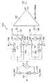
図1Aおよび図1Bは、時間変化包絡線および位相複素入力信号の生成を説明する例である。図1Aでは、時間変化包絡線搬送波信号104、106が、位相コントローラ110に入力される。位相コントローラ110は、信号104、106の位相成分を操作する。言い換えると、位相コントローラ110は、信号104、106を位相シフトすることができる。したがって、結果の信号108、112は、信号104、106に対して位相シフトされていることになる。図1Aの例では、信号108、112から分かるように、位相コントローラ110は、時刻刻t0に、信号104、106において位相反転(180度位相シフト)を引き起こす。信号108、112は、時間変化複素搬送波信号を表す。信号108、112は、時間変化包絡線および位相成分の両方を有する。信号108、112は、合算されると、信号114をもたらす。信号114も、時間変化複素信号を表す。信号114は、本発明のVPA実施形態への入力信号例(例えば、図50のステップ504への入力例)とすることができる。1.1) Generation Example of Complex Envelope Time-Varying Input Signal FIGS. 1A and 1B are examples illustrating generation of a time-varying envelope and a phase complex input signal. In FIG. 1A, time-varying envelope carrier signals 104, 106 are input to phase
時間変化複素信号は、図1Bに示されるように、生成されることもできる。図1Bでは、信号116、118は、ベースバンド信号を表す。例えば、信号116、118は、信号の同相(I)および直交(Q)ベースバンド成分とすることができる。図1Bの例では、信号116、118は、+1から−1に移行する際にゼロ交差を受ける。信号116、118は、信号120によって、または90度位相シフトされた信号120によって乗算される。信号116は、信号120の0度シフト・バージョン(0 degree shifted version)によって乗算される。信号118は、信号120の90度シフト・バージョン(90 degree shifted version)によって乗算される。結果の信号122、124は、時間変化複素搬送波信号を表す。信号122、124が、信号116、118の時間変化振幅に従って変化する包絡線を有することに留意されたい。さらに、信号122、124はともに、信号116、118のゼロ交差のところで、位相反転を受ける。信号122、124は、合算されて、信号126をもたらす。信号126は、時間変化複素信号を表す。信号126は、本発明のVPA実施形態への入力信号例を表すことができる。加えて、信号116、118も、本発明のVPA実施形態への入力信号例を表すことができる。 A time-varying complex signal can also be generated as shown in FIG. 1B. In FIG. 1B, signals 116 and 118 represent baseband signals. For example, the
1.2)時間変化複素包絡線信号の一定包絡線信号からの生成例
このセクションの説明は、一般に、図50のステップ508の動作に関する。図1Cは、時間変化複素信号の、2つ以上の実質的に一定の包絡線信号の和からの生成についての3つの例を説明する。しかし、本明細書で提供される教示に基づいて、図1Cの例で説明される概念が、2つ以上の一定包絡線信号の場合にも同様に拡張され得ることは、当業者であれば理解されよう。1.2) Example Generation of Time-Varying Complex Envelope Signal from Constant Envelope Signal The description in this section generally relates to the operation of
図1Cの例1では、一定包絡線信号132、134が、位相コントローラ130に入力される。位相コントローラ130は、信号132、134の位相成分を操作して、それぞれ信号136、138を生成する。信号136、138は、実質的に一定の包絡線信号を表し、信号140を生成するために合算される。例1に関連する図1Cのフェーザー(phasor)表現は、信号136、138をそれぞれフェーザーP136、P138として示す。信号140は、フェーザーP140として示される。例1では、P136、P138は、フェーザー表現の実軸に揃えられると仮定される基準信号に対して、角度φ1だけ対称的に位相シフトされている。それに対応して、時間領域信号136、138は、等しい量だけ、しかし基準信号に対して互いに逆方向に位相シフトされる。したがって、P136とP138の和であるP140は、基準信号と同相である。In Example 1 of FIG. 1C, constant envelope signals 132 and 134 are input to the
図1Cの例2では、実質的に一定の包絡線信号132、134は、位相コントローラ130に入力される。位相コントローラ130は、信号132、134の位相成分を操作して、それぞれ信号142、144を生成する。信号142、144は、実質的に一定の包絡線信号を表し、信号150を生成するために合算される。例2に関連するフェーザー表現は、信号142、144をそれぞれフェーザーP142、P144として示す。信号150は、フェーザーP150として示される。例2では、P142、P144は、基準信号に対して対称的に位相シフトされている。したがって、P140と同様に、P150も基準信号と同相である。しかし、P142、P144は、基準信号に対してφ2≠φ1である角度だけ位相シフトされている。その結果、P150は、例1のP140とは異なる大きさを有する。時間領域表現では、信号140、150は、同相であるが、互いに対して異なる振幅を有することに留意されたい。In example 2 of FIG. 1C, substantially constant envelope signals 132, 134 are input to phase
図1Cの例3では、実質的に一定の包絡線信号132、134は、位相コントローラ130に入力される。位相コントローラ130は、信号132、134の位相成分を操作して、それぞれ信号146、148を生成する。信号146、148は、実質的に一定の包絡線信号を表し、信号160を生成するために合算される。例3に関連するフェーザー表現は、信号146、148をそれぞれフェーザーP146、P148として示す。信号160は、フェーザーP160として示される。例3では、P146は、基準信号に対して角度φ3だけ位相シフトされている。P148は、基準信号に対して角度φ4だけ位相シフトされており、φ3とφ4は、等しくても、または等しくなくてもよい。したがって、P146とP148の和であるP160は、もはや基準信号と同相ではない。P160は、基準信号に対して角度Θだけ位相シフトされている。同様に、P160は、例1および例2のP140およびP150に対してΘだけ位相シフトされている。P160は、図3に示されるように、P140に対して振幅が変化することもできる。In example 3 of FIG. 1C, substantially constant envelope signals 132, 134 are input to phase
要約すると、図1Cの例は、時間変化振幅信号が、2つ以上の実質的に一定の包絡線信号の和によって獲得され得ることを示している(例1)。さらに、時間変化信号は、2つ以上の実質的に一定の包絡線信号を逆方向に等しくシフトすることによっては、振幅変化をもつことができるが、それに与えられる位相変化をもつことはできない(例2)。信号の2つ以上の一定の包絡線構成要素を同じ方向に等しくシフトすると、時間変化信号に対して、振幅変化なしで位相変化を与えることができる。任意の時間変化振幅および位相信号が、2つ以上の実質的に一定の包絡線信号を使用して、生成されることができる(例3)。 In summary, the example of FIG. 1C shows that a time-varying amplitude signal can be obtained by the sum of two or more substantially constant envelope signals (Example 1). Furthermore, a time-varying signal can have an amplitude change by equally shifting two or more substantially constant envelope signals in the opposite direction, but not a phase change given to it ( Example 2). Shifting two or more constant envelope components of the signal equally in the same direction can give the time-varying signal a phase change without an amplitude change. Any time-varying amplitude and phase signal can be generated using two or more substantially constant envelope signals (Example 3).
図1Cの例の信号は、説明の目的でのみ正弦波形として示されていることに留意されたい。本明細書の教示に基づいて、その他のタイプの波形も使用され得ることは、当業者であれば理解されよう。図1Cの例は、説明の目的でのみ本明細書で提供され、本発明の特定の実施形態に対応してもよく、または対応しなくてもよいことも留意されるべきである。 Note that the signal of the example of FIG. 1C is shown as a sinusoidal waveform for illustrative purposes only. Those skilled in the art will appreciate that other types of waveforms may be used based on the teachings herein. It should also be noted that the example of FIG. 1C is provided herein for illustrative purposes only, and may or may not correspond to a particular embodiment of the invention.
1.3)ベクトル電力増幅の概要
ベクトル電力増幅の高水準の概要が、今から提供される。図1Dは、例示的な時間変化複素入力信号172の電力増幅を示している。図1Aおよび図1Bで説明されたような信号114および126は、信号172の例とすることができる。さらに、信号172は、104および106(図1A)、108および112(図1A)、116および118(図1B)、ならびに122および124(図1B)など、2つ以上の構成要素信号によって生成されることができ、または2つ以上の成分信号から構成されることができる。1.3) Vector power amplification overview A high level overview of vector power amplification is now provided. FIG. 1D illustrates power amplification of an exemplary time-varying
図1Dの例では、VPA170は、本発明によるVPAシステム実施形態を表す。VPA170は、信号172を増幅して、増幅出力信号178を生成する。出力信号178は、最小歪みしかをもたないように効率的に増幅される。 In the example of FIG. 1D,
図1Dの例では、信号172および178は、それぞれ電圧信号Vin(t)およびVolt(t)を表す。任意の時刻刻において、図1Dの例では、Vin(t)およびVolt(t)は、Kがスケール係数(scale factor)であり、t’がVPAシステムに存在する可能性のある時間遅延を表すとした場合に、Volt(t)=Kevin(tat’)となるように関係付けられる。電力の意味合いでは、In the example of FIG. 1D, signals 172 and 178 represent voltage signals Vin (t) and Volt (t), respectively. At any time instant, in the example of FIG. 1D, Vin (t) and Volt (t) are time delays where K is a scale factor and t ′ may be present in the VPA system.Is expressed so that Volt (t) = Kevin (tat ′). In terms of electricity,
であり、出力信号178は、入力信号172の電力増幅されたバージョンである。And the
図1Dに示されるような、時間変化複素信号の線形(または実質的に線形)な電力増幅は、図1Eに示されるような本発明の実施形態によって達成される。 Linear (or substantially linear) power amplification of a time-varying complex signal, as shown in FIG. 1D, is achieved by an embodiment of the present invention as shown in FIG. 1E.
図1Eは、本発明の実施形態によるベクトル電力増幅実施形態を概念的に説明するブロック図例である。図1Eでは、入力信号172は、時間変化複素信号を表す。例えば、入力信号172は、図1Aおよび図1Bで説明されたように生成されることができる。実施形態では、信号172は、デジタルまたはアナログ信号とすることができる。さらに、信号172は、ベースバンドまたは搬送波ベース信号(carrier-based signal)とすることができる。 FIG. 1E is an example block diagram conceptually illustrating a vector power amplification embodiment according to an embodiment of the present invention. In FIG. 1E, the
図1Eを参照すると、本発明の実施形態によれば、入力信号172またはその同等物が、VPA182に入力される。図1Eの実施形態では、VPA182は、状態機械(state machine)184およびアナログ回路186を含む。状態機械184は、デジタルおよび/またはアナログ構成要素を含むことができる。アナログ回路186は、アナログ構成要素を含むことができる。VPA182は、図1Eに示されるように、入力信号172を処理して、2つ以上の信号188−{1,...,n}を生成する。図1Cで信号136、138、142、144、および146、148に関して説明されたように、信号188−{1,...,n}は、異なる期間にわたって、互いに対して位相シフトされても、または位相シフトされなくてもよい。さらに、VPA182は、信号188−{1,...,n}の和が、ある種の実施形態で信号172の増幅されたバージョン(amplified version)とすることができる信号194を生じさせるように、信号188−{1,...,n}を生成する。 Referring to FIG. 1E, according to an embodiment of the present invention, an
図1Eを続けて参照すると、信号188−{1,...,n}は、実質的に一定の包絡線信号である。したがって、先の段落の説明は、図50のステップ504に対応する。 With continued reference to FIG. 1E, signals 188- {1,. . . , N} is a substantially constant envelope signal. Therefore, the description in the previous paragraph corresponds to step 504 in FIG.
図1Eの例では、一般に図50のステップ506に対応して、一定包絡線信号188−{1,...,n}は各々、対応する電力増幅器(PA)190−{1,...,n}によって独立に増幅されて、増幅された信号192−{1,...,n}を生成する。実施形態では、PA190−{1,...,n}は、実質的に等しいそれぞれの一定包絡線信号188−{1,...,n}を増幅する。増幅された信号192−{1,...,n}は、実質的に一定の包絡線信号であり、ステップ508で、合算されて、出力信号194を生成する。出力信号194が、入力信号172の線形(または実質的に線形)に増幅されたバージョンであることができることに留意されたい。出力信号194は、本明細書で説明されるように、入力信号172の周波数アップコンバート・バージョン(frequency-upconverted version)であることもできる。 In the example of FIG. 1E, generally corresponding to step 506 of FIG. 50, constant envelope signals 188- {1,. . . , N} each correspond to a corresponding power amplifier (PA) 190- {1,. . . , N} and amplified signals 192- {1,. . . , N}. In the embodiment, PA190- {1,. . . , N} are the respective constant envelope signals 188- {1,. . . , N}. The amplified signals 192- {1,. . . , N} are substantially constant envelope signals that are summed at
2.一般的な数学的概要
2.1)フェーザー信号表現
図1は、信号r(t)のフェーザー表現2. General Mathematical Overview 2.1) Phasor Signal Representation Figure 1 shows the phasor representation of the signal r (t).
102を示している。信号のフェーザー表現は、信号の包絡線の振幅(magnitude)および基準信号に対する信号の位相シフトを明示的に表現する。本文書では、限定のためではなく便宜的に、基準信号は、フェーザー表現の直交空間の実(Re)軸に揃えられるものとして定義される。しかし、本発明は、この実施形態に限定されない。信号の周波数情報は、この表現では暗黙に決まっており、基準信号の周波数によって与えられる。例えば、図1を参照し、実軸がcos(ωt)基準信号に対応すると仮定すると、フェーザー102 is shown. The phasor representation of the signal explicitly represents the amplitude of the signal envelope and the phase shift of the signal relative to the reference signal. In this document, for convenience and not limitation, the reference signal is defined as being aligned with the real (Re) axis of the orthogonal space of the phasor representation. However, the present invention is not limited to this embodiment. The frequency information of the signal is implicit in this representation and is given by the frequency of the reference signal. For example, referring to FIG. 1, assuming that the real axis corresponds to a cos (ωt) reference signal,
は、関数r(t)=R(t)cos(ωt+φ(t))に変換され、ここでRはIs converted to the function r (t) = R (t) cos (ωt + φ (t)), where R is
の大きさ(magnitude)である。Is the magnitude.
図1を続けて参照すると、フェーザー Continuing to refer to FIG. 1, the phaser
は、実部フェーザーThe real part phaser
および虚部フェーザーAnd imaginary phaser
に分解されることができる。Can be broken down into.
およびand
は、基準信号に関するIs related to the reference signal
の同相および直交フェーザー成分であると言われる。さらに、Are said to be in-phase and quadrature phasor components. further,
およびand
に対応する信号は、それぞれI(t)=R(t)・cos(φ(t))およびQ(t)=R(t)・sin(φ(t))として、r(t)に関係付けられることに留意されたい。時間領域では、信号r(t)は、同相および直交成分によって以下のように書き表されることもできる。
r(t)=I(t)・cos(ωt)+Q(t)・sin(ωt)=
R(t)・cos(φ(t))・cos(ωt)+R(t)・sin(φ(t))・sin(ωt) (1)
図1の例では、R(t)は、特定の時刻において示されていることに留意されたい。Are related to r (t) as I (t) = R (t) · cos (φ (t)) and Q (t) = R (t) · sin (φ (t)), respectively. Note that it is attached. In the time domain, the signal r (t) can also be written in terms of in-phase and quadrature components as follows:
r (t) = I (t) · cos (ωt) + Q (t) · sin (ωt) =
R (t) · cos (φ (t)) · cos (ωt) + R (t) · sin (φ (t)) · sin (ωt) (1)
Note that in the example of FIG. 1, R (t) is shown at a particular time.
2.2)時間変化複素包絡線信号
図2は、2つの異なる時刻t1およびt2における、信号r(t)のフェーザー表現を示している。信号の包絡線の振幅で表されるフェーザーの大きさおよびその相対位相シフトはともに、時間t1から時間t2にかけて変化する。図2では、これは、フェーザー2.2) Time-varying complex envelope signal FIG. 2 shows a phasor representation of the signal r (t) at two different times t1 and t2. Both the magnitude of the phasor represented by the amplitude of the signal envelope and its relative phase shift vary from time t1 to time t2. In Figure 2, this is the phaser
およびand
の変化する大きさ、ならびに対応する位相シフト角(phase shift angle)φ1およびφ2によって示されている。したがって、信号r(t)は、時間変化複素包絡線信号である。And the corresponding phase shift angles φ1 and φ2 . Therefore, the signal r (t) is a time-varying complex envelope signal.
さらに、図2から、信号r(t)の実数部および虚数部のフェーザー成分も、振幅について時間変化することに留意されたい。したがって、それらの対応する時間領域信号(time domain signals)も、時間変化包絡線を有する。 Furthermore, it should be noted from FIG. 2 that the phasor components of the real and imaginary parts of the signal r (t) also vary with time in amplitude. Accordingly, their corresponding time domain signals also have time-varying envelopes.
図3A〜図3Cは、時間変化複素包絡線信号を生成するための変調例を示している。図3Aは、信号m(t)の図である。図3Bは、搬送波信号c(t)の部分の図である。図3Cは、信号m(t)およびc(t)の乗算から得られる信号r(t)を示している。 3A to 3C show modulation examples for generating a time-varying complex envelope signal. FIG. 3A is a diagram of the signal m (t). FIG. 3B is a diagram of a portion of the carrier signal c (t). FIG. 3C shows the signal r (t) resulting from the multiplication of the signals m (t) and c (t).
図3Aの例では、信号m(t)は、大きさが時間変化する信号である。m(t)はさらに、ゼロ交差を受ける。搬送波信号c(t)は、図3Bの例では、一般に信号m(t)の周波数より高いある搬送波周波数で振動している。 In the example of FIG. 3A, the signal m (t) is a signal whose magnitude changes with time. m (t) further undergoes a zero crossing. In the example of FIG. 3B, the carrier signal c (t) oscillates at a carrier frequency that is generally higher than the frequency of the signal m (t).
図3Cから、結果の信号r(t)が時間変化包絡線を有することが認められ得る。さらに図3Cから、変調信号m(t)がゼロ交差する瞬間に、r(t)が位相反転を受けることにも留意されたい。一定でない包絡線および位相をともにもつ場合、r(t)は、時間変化複素包絡線信号であると言われる。 From FIG. 3C, it can be seen that the resulting signal r (t) has a time-varying envelope. It should also be noted from FIG. 3C that r (t) undergoes phase reversal at the moment the modulation signal m (t) crosses zero. If both have a non-constant envelope and phase, r (t) is said to be a time-varying complex envelope signal.
2.3)時間変化包絡線信号の一定包絡線分解
大きさおよび位相が時間変化する任意のフェーザーは、基準フェーザーに対して適切に指定された位相シフトを有する、2つ以上の一定の大きさのフェーザーの合算によって、獲得されることができる。2.3) Constant envelope decomposition of time-varying envelope signal Any phasor whose magnitude and phase are time-varying has two or more constant magnitudes with appropriately specified phase shifts relative to the reference phasor. It can be obtained by adding together the phasers.
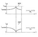
図3Dは、時間変化包絡線および位相信号S(t)の例の図を示している。説明を簡単にするため、信号S(t)は、最大包絡線振幅Aを有する正弦信号であると仮定する。図3Dはさらに、2つの一定包絡線信号S1(t)およびS2(t)の和によって、任意の時刻において、信号S(t)がどのように獲得され得るかの例を示している。一般に、S1(t)=A1sin(ωt+φ1(t))であり、S1(t)=A2sin(ωt+φ2(t))である。FIG. 3D shows a diagram of an example of a time-varying envelope and a phase signal S (t). For simplicity of explanation, it is assumed that the signal S (t) is a sinusoidal signal having a maximum envelope amplitude A. FIG. 3D further shows an example of how the signal S (t) can be obtained at any time by the sum oftwo constant envelope signals S1 (t) and S2 (t). . In general, S1 (t) = A1 sin (ωt + φ1 (t)) and S1 (t) = A2 sin (ωt + φ2 (t)).
説明の目的で、信号S1(t)およびS2(t)をS(t)に対して適切に位相調整(phase)することによって、S(t)=K(S1(t)+S2(t))(Kは定数)となるように、S1(t)およびS2(t)がどのように合算され得るかを説明する3つの図が、図3Dに提供されている。言い換えると、信号S(t)は、任意の時刻に、2つ以上の信号に分解されることができる。図3Dから、期間T1の間、S1(t)およびS2(t)はともに、信号S(t)に対して同相であり、したがって、合算すると信号S(t)の最大包絡線振幅Aになる。しかし、期間T3の間、S1(t)およびS2(t)は、互いに対して180度位相がずれており、したがって、合算すると信号S(t)の最小包絡線振幅になる。For purposes of illustration, S (t) = K (S1 (t) + S2 by appropriately phasing the signals S1 (t) and S2 (t) with respect to S (t). Three diagrams are provided in FIG. 3D that illustrate how S1 (t) and S2 (t) can be summed so that (t)) (K is a constant). In other words, the signal S (t) can be decomposed into two or more signals at any time. From FIG. 3D, during period T1 , S1 (t) and S2 (t) are both in phase with signal S (t), and therefore, when combined, the maximum envelope amplitude of signal S (t) Become A. However, during period T3 , S1 (t) and S2 (t) are 180 degrees out of phase with each other, and therefore add up to the minimum envelope amplitude of signal S (t).
図3Dの例は、正弦波信号の場合を説明している。しかし、フーリエ級数またはフーリエ変換によって表すことができる搬送波信号を変調する任意の時間変化包絡線も同様に、2つ以上の実質的に一定の包絡線信号に分解することができることは、当業者であれば理解されよう。したがって、複数の実質的に一定の包絡線信号の位相を制御することによって、任意の時間変化複素包絡線信号を生成することができる。 The example of FIG. 3D describes the case of a sine wave signal. However, it will be appreciated by those skilled in the art that any time-varying envelope that modulates a carrier signal that can be represented by a Fourier series or Fourier transform can similarly be decomposed into two or more substantially constant envelope signals. If you can understand it. Thus, any time-varying complex envelope signal can be generated by controlling the phase of a plurality of substantially constant envelope signals.
3.ベクトル電力増幅方法およびシステム
本発明の実施形態によるベクトル電力増幅方法およびシステムは、任意の時間変化包絡線信号を2つ以上の実質的に一定の包絡線構成要素信号に分解する能力、またはそのような構成要素信号を受け取りもしくは生成し、構成要素信号を増幅し、その後、増幅された信号を合算して、時間変化複素包絡線信号の増幅バージョン(amplified version)を生成する能力に依存する。3. Vector Power Amplification Method and System The vector power amplification method and system according to embodiments of the present invention is capable of decomposing any time-varying envelope signal into two or more substantially constant envelope component signals, or the like. Depending on the ability to receive or generate a component signal, amplify the component signal, and then add the amplified signals to generate an amplified version of the time-varying complex envelope signal.
セクション3.1〜3.3で、4ブランチ(4−branch)および2ブランチ(2−branch)実施形態を含む、本発明のベクトル電力増幅(VPA)実施形態が提供される。この説明において、各VPA実施形態は、先ず、実施形態の基礎をなす概念の数学的誘導を使用して、概念的に提示される。次に、VPA実施形態の動作方法の実施形態が提示され、続いて、VPA実施形態の様々なシステム・レベルの実施形態が提示される。 In sections 3.1-3.3, vector power amplification (VPA) embodiments of the present invention are provided, including 4-branch and 2-branch embodiments. In this description, each VPA embodiment is first presented conceptually using a mathematical derivation of the concept underlying the embodiment. Next, an embodiment of a method of operation of the VPA embodiment is presented, followed by various system level embodiments of the VPA embodiment.
セクション3.4は、本発明の実施形態による制御モジュールの様々な実施形態を提示する。本発明の実施形態による制御モジュールは、本発明のある種のVPA実施形態を可能にするために使用されることができる。いくつかの実施形態では、制御モジュールは、VPA実施形態の入力ステージと、VPA実施形態の後続のベクトル変調ステージとの間にある中間モジュールである。 Section 3.4 presents various embodiments of the control module according to embodiments of the present invention. A control module according to embodiments of the present invention can be used to enable certain VPA embodiments of the present invention. In some embodiments, the control module is an intermediate module between the input stage of the VPA embodiment and the subsequent vector modulation stage of the VPA embodiment.
セクション3.5は、本発明の実施形態によるVPA出力ステージ実施形態を説明する。出力ステージ実施形態は、VPA実施形態の出力信号を生成することに関する。 Section 3.5 describes VPA output stage embodiments according to embodiments of the present invention. The output stage embodiment relates to generating the output signal of the VPA embodiment.
セクション3.6は、本発明の実施形態による高調波制御に関する。高調波制御は、本発明のある種の実施形態において実装して、VPA実施形態の高調波における実数部および虚数部の電力を操作し、その結果、出力において基本周波数に存在する電力を増大させることができる。 Section 3.6 relates to harmonic control according to embodiments of the present invention. Harmonic control is implemented in certain embodiments of the present invention to manipulate the real and imaginary powers in the harmonics of the VPA embodiment, thus increasing the power present at the fundamental frequency at the output. be able to.
セクション3.7は、本発明の実施形態による電力制御に関する。電力制御は、本発明のVPA実施形態を利用することができる応用例の電力レベル要件を満たすために、本発明のある種の実施形態に実装することができる。 Section 3.7 relates to power control according to embodiments of the present invention. Power control can be implemented in certain embodiments of the present invention to meet the power level requirements of applications that can utilize the VPA embodiments of the present invention.
3.1)カルテシアン4ブランチ・ベクトル電力増幅器
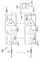
限定のためではなく説明を容易にするために本明細書でカルテシアン4ブランチ(Cartesian 4-Branch)VPA実施形態と呼ばれる、本発明の一実施形態によれば、時間変化複素包絡線信号は、4つの実質的に一定の包絡線構成要素信号に分解される。構成要素信号は、等しくまたは実質的に等しく個別に増幅され、その後、元の時間変化複素包絡線信号の増幅バージョンを構成するために合算される。3.1) Cartesian 4-Branch Vector Power Amplifier An embodiment of the present invention, referred to herein as a Cartesian 4-Branch VPA embodiment for ease of explanation and not limitation The time-varying complex envelope signal is decomposed into four substantially constant envelope component signals. The component signals are amplified individually equally or substantially equally and then summed to form an amplified version of the original time-varying complex envelope signal.
この実施形態では、限定のためではなく説明の目的で、4ブランチが利用されることに留意されたい。本発明の範囲は、その他の数のブランチの使用を包含し、そのような変形の実装は、本明細書に含まれる教示に基づいて、当業者には明らかであろう。 Note that in this embodiment, four branches are utilized for purposes of illustration and not limitation. The scope of the invention encompasses the use of other numbers of branches, and the implementation of such variations will be apparent to those skilled in the art based on the teachings contained herein.
一実施形態では、時間変化複素包絡線信号は、最初にその同相および直交ベクトル成分に分解される。フェーザー表現では、同相および直交ベクトル成分は、それぞれ信号の実数部および虚数部の各フェーザーに対応する。 In one embodiment, the time-varying complex envelope signal is first decomposed into its in-phase and quadrature vector components. In phasor representation, the in-phase and quadrature vector components correspond to the phasors of the real and imaginary parts of the signal, respectively.
上で説明されたように、信号の同相および直交ベクトル成分の大きさは、信号の振幅に比例して変化し、したがって、信号が時間変化包絡線信号である場合、一定包絡線ではない。したがって、4ブランチVPA実施形態はさらに、信号の同相および直交ベクトル成分の各々を、2つは同相信号成分用、2つは直交信号成分用の、4つの実質的に一定の包絡線成分に分解する。この概念は、フェーザー信号表現を使用して、図4で説明される。 As explained above, the magnitude of the in-phase and quadrature vector components of the signal varies in proportion to the amplitude of the signal, and therefore is not a constant envelope when the signal is a time-varying envelope signal. Thus, the four-branch VPA embodiment further divides each of the in-phase and quadrature vector components of the signal into four substantially constant envelope components, two for the in-phase signal component and two for the quadrature signal component. Decompose. This concept is illustrated in FIG. 4 using a phasor signal representation.
図4の例では、フェーザー In the example of FIG.
およびand
は、それぞれ2つの時刻t1およびt2における、例示的な時間変化複素包絡線信号の実数部フェーザーに対応する。フェーザーCorresponds to the real part phasor of the exemplary time-varying complex envelope signal at two times t1 and t2, respectively. Phaser
およびand
が異なる大きさをもつことに留意されたい。Note that has different sizes.
図4を続けて参照すると、瞬間t1において、フェーザー With continued reference to FIG. 4, at the instant t1, the phaser
は、上側および下側フェーザーThe upper and lower phasers
およびand
の合算によって、獲得されることができる。同様に、瞬間t2において、フェーザーCan be obtained by adding together. Similarly, at the instant t2, the phaser
は、上側および下側フェーザーThe upper and lower phasers
およびand
の合算によって、獲得されることができる。フェーザーCan be obtained by adding together. Phaser
およびand
が、等しいまたは実質的に等しい大きさをもつことに留意されたい。同様に、フェーザーNote that are equal or substantially equal in magnitude. Similarly, phaser
およびand
も、実質的に等しい大きさをもつ。したがって、時間変化包絡線信号の実数部フェーザーは、少なくとも2つの実質的に一定の包絡線成分の合算によって、任意の時刻に獲得されることができる。Have substantially the same size. Thus, the real part phasor of the time-varying envelope signal can be obtained at any time by the sum of at least two substantially constant envelope components.
に対するフェーザーAgainst phasor
およびand
の位相シフト、ならびにPhase shift, and
に対するフェーザーAgainst phasor
およびand
の位相シフトは、それぞれフェーザーPhase shift of each phaser
およびand
の所望する大きさに従って設定される。1つのケースでは、上側および下側フェーザーが等しい大きさをもつように選択される場合、上側および下側フェーザーは、フェーザーに対して対称的に位相シフトされる。これは、図4の例に示されており、すべてが等しい大きさをもつIs set according to the desired size. In one case, if the upper and lower phasors are selected to have equal magnitude, the upper and lower phasors are phase shifted symmetrically with respect to the phasor. This is shown in the example of FIG. 4 and all have the same size
およびand
に対応する。第2のケースでは、上側および下側フェーザーの位相シフトは、フェーザーに対して実質的に対称的に位相シフトされる。本明細書の説明に基づいて、上側および下側フェーザーの大きさおよび位相シフトが正確に等しい値である必要はないことは、当業者であれば理解されよう。Corresponding to In the second case, the phase shifts of the upper and lower phasors are phase shifted substantially symmetrically with respect to the phasor. One skilled in the art will appreciate that based on the description herein, the magnitude and phase shift of the upper and lower phasors need not be exactly equal.
一例として、図4に示されたケースについて、図4で、 As an example, for the case shown in FIG.
およびand
として示される相対位相シフトは、正規化されたフェーザーRelative phase shifts shown as normalized phaser
およびand
の大きさに関係付けられ得ることが、さらに確認されることができる。It can be further confirmed that it can be related to
ここで、I1およびI2は、それぞれフェーザーWhere I1 and I2 are phasers
およびand
の正規化された大きさを表し、I1およびI2の定義域は、式(2)および(3)が有効である定義域に従って適切に制限される。式(2)および(3)は、相対位相シフトを正規化された大きさに関係付けるための1つの表現であることに留意されたい。式(2)および(3)のその他の解法、等価表現、および/または簡略化表現も、利用されることができる。相対位相シフトを正規化された大きさに関係付ける検索表が、使用されることもできる。The domain of I1 and I2 is appropriately restricted according to the domain in which equations (2) and (3) are valid. Note that equations (2) and (3) are one representation for relating the relative phase shift to the normalized magnitude. Other solutions, equivalent representations, and / or simplified representations of equations (2) and (3) can also be utilized. A look-up table relating the relative phase shift to the normalized magnitude can also be used.
上で説明された概念は同様に、図4に示されるように、信号r(t)の虚数部のフェーザーまたは直交成分部分にも適用されることができる。したがって、任意の時刻tにおいて、信号r(t)の虚フェーザー部分 The concepts described above can also be applied to the phasor or quadrature component part of the imaginary part of the signal r (t), as shown in FIG. Therefore, at an arbitrary time t, the imaginary phasor portion of the signal r (t)
は、実質的に等しいまたは一定の大きさの上側および下側フェーザー成分Is the upper and lower phasor components of substantially equal or constant magnitude
およびand
を合算することによって、獲得されることができる。この例では、Can be obtained by adding together. In this example,
およびand
は、時間tにおけるAt time t
の大きさに従って設定される角度だけ、Only the angle set according to the size of
に対して対称的に位相シフトされる。Phase shifted symmetrically.
およびand
の所望するフェーザーDesired phaser
に対する関係は、I1およびI2をそれぞれQ1およびQ2で置き換えることによって、式2および3で定義されるように関係付けられる。Is related as defined in
上の説明から、フェーザー表現では、大きさおよび位相が可変の任意のフェーザー From the above explanation, in the phasor representation, any phasor with variable size and phase
は、以下のように、4つの実質的に大きさが一定のフェーザー成分の合算によって構成され得ることが導かれ、Is derived from the summation of four substantially constant phasor components as follows:
ここで、IU、IL、QU、およびQLは、それぞれフェーザーWhere IU , IL , QU , and QL are the phasers
およびand
の大きさを表す。Represents the size of.
それに対応して、時間領域では、時間変化複素包絡線正弦信号r(t)=R(t)cos(ωt+φ)は、以下のように、4つの一定の包絡線信号の和によって構成される。 Correspondingly, in the time domain, the time-varying complex envelope sine signal r (t) = R (t) cos (ωt + φ) is composed of the sum of four constant envelope signals as follows:
ここで、here,
は、Is
が正の実軸と同相か、それとも180°位相がずれているかに依存する。同様に、Depends on whether they are in phase with the positive real axis or 180 ° out of phase. Similarly,
は、Is
が虚軸と同相か、それとも180°位相がずれているかに依存する。Depends on whether is in phase with the imaginary axis or 180 ° out of phase.
は、実軸に対するIs relative to the real axis
およびand
の位相シフトに対応する。同様に、Corresponds to the phase shift. Similarly,
は、虚軸に対するIs for the imaginary axis
およびand
の位相シフトに対応する。Corresponds to the phase shift.
およびand
は、(2)および(3)で与えられる式を使用して、算出されることができる。Can be calculated using the equations given in (2) and (3).
式(5)は、以下のように、さらに簡略化されることができる。 Equation (5) can be further simplified as follows.
ここで、here,
およびand
である。It is.
式(5)および式(6)の時間領域表現は正弦波形の場合について提供されたが、非正弦波形についても、適切な基底関数(basis function)を使用して、等価表現が展開できることは、当業者であれば理解できよう。さらに、当業者であれば本明細書の教示に基づいて理解されるように、上で説明された実質的に一定の包絡線信号への2次元分解は、多次元分解に適切に拡張されることができる。 Although the time domain representations of Equations (5) and (6) have been provided for sinusoidal waveforms, the equivalent representation can be expanded for non-sinusoidal waveforms using an appropriate basis function. Those skilled in the art will understand. Further, as those skilled in the art will appreciate based on the teachings herein, the two-dimensional decomposition into substantially constant envelope signals described above is suitably extended to multi-dimensional decomposition. be able to.
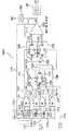
図5は、カルテシアン4ブランチVPA実施形態のブロック図例である。所望する電力レベルおよび周波数特性の出力信号r(t)578が、カルテシアン4ブランチVPA実施形態によるベースバンド同相および直交成分から生成される。 FIG. 5 is a block diagram example of a Cartesian 4-branch VPA embodiment. An output signal r (t) 578 of the desired power level and frequency characteristics is generated from the baseband in-phase and quadrature components according to the Cartesian 4-branch VPA embodiment.
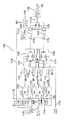
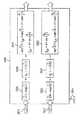
図5の例では、シンセサイザ510などの周波数ジェネレータが、出力信号r(t)578のものと同じ周波数をもつ基準信号A*cos(ωt)511を生成する。基準信号の選択が所望する出力信号に従って行われることは、当業者であれば理解できよう。例えば、所望する出力信号の所望する周波数が2.4GHzである場合、基準信号の周波数は、2.4GHzに設定される。このようにして、本発明の実施形態は、周波数アップ・コンバージョンを達成する。 In the example of FIG. 5, a frequency generator such as
図5を参照すると、1つまたは複数の位相スプリッタが使用されて、基準信号511に基づいて信号521、531、541および551を生成する。図5の例では、これは、位相スプリッタ512、514、516を使用し、各位相スプリッタにおいて0°の位相シフトが適用されることによって、行われる。しかし、基準信号511から信号521、531、541、551を生成するために様々な技法が使用され得ることは、当業者であれば理解されよう。例えば、単一ステップで4つの複製信号(replica)521、531、541、551を生成するために、1:4位相スプリッタが使用されることができ、あるいは、図5の実施形態例では、信号511は、信号521、531、541、551に直接結合されることができる。実施形態に応じて、所望する信号521、531、541、551をもたらすために、様々な位相スプリッタが適用されることもできる。 Referring to FIG. 5, one or more phase splitters are used to generate signals 521, 531, 541 and 551 based on the reference signal 511. In the example of FIG. 5, this is done by using
図5を続けて参照すると、信号521、531、541、551の各々は、それぞれ対応するベクトル変調器520、530、540、550に提供される。ベクトル変調器520、530、540、550は、適切な入力信号を用いて、式(6)で提供される式に従って、信号r(t)の4つの一定包絡線構成要素を生成する。図5の実施形態例では、ベクトル変調器520および530は、それぞれ信号r(t)のIU(t)およびIL(t)成分を生成する。同様に、ベクトル変調器540および550は、それぞれ信号r(t)のQU(t)およびQL(t)成分を生成する。With continued reference to FIG. 5, each of the signals 521, 531, 541, 551 is provided to a
各ベクトル変調器520、530、540、550の実際の実装は、様々であることができる。例えば、(6)の式による一定包絡線構成要素を生成するために様々な技法が存在することは、当業者であれば理解されよう。 The actual implementation of each
図5の実施形態例では、各ベクトル変調器520、530、540、550は、信号522、531、541、551を位相調整するための入力位相スプリッタ522、532、542、552を含む。したがって、同相および直交成分、またはそれぞれの入力信号を生成するために、入力位相スプリッタ522、532、542、552が使用される。 In the example embodiment of FIG. 5, each
各ベクトル変調器520、530、540、550では、同相および直交成分が、振幅情報と乗算される。図5では、例えば、乗算器524は、信号521の直交成分を、IU(t)の直交振幅情報IUYと乗算する。並列して、乗算器526は、同相複製信号を、IU(t)の同相振幅情報sgn(I)×IUXと乗算する。In each
IU(t)の一定包絡線構成要素を生成するため、信号525および527が、位相スプリッタ528または代替合算技法を使用して合算される。結果の信号529は、信号r(t)のIU(t)成分に対応する。Signals 525 and 527 are summed using
上で説明されたのと同様の方法で、ベクトル変調器530、540、550は、それぞれ信号r(t)のIL(t)、QU(t)、およびQL(t)成分を生成する。IL(t)、QU(t)、およびQL(t)は、それぞれ図5の信号539、549、559に対応する。In a manner similar to that described above,
さらに、上で説明されたように、信号529、539、549、559は、実質的に等しくかつ一定の振幅の包絡線を有することによって特徴付けられる。したがって、信号529、539、549、559が対応する電力増幅器(PA)562、564、566、568に入力されるとき、対応する増幅された信号563、565、567、569は、実質的に一定の包絡線信号である。 Further, as explained above, the signals 529, 539, 549, 559 are characterized by having substantially equal and constant amplitude envelopes. Thus, when signals 529, 539, 549, 559 are input to corresponding power amplifiers (PA) 562, 564, 566, 568, the corresponding amplified signals 563, 565, 567, 569 are substantially constant. Is an envelope signal.
電力増幅器562、564、566、568は、それぞれ各信号529、539、549、559を増幅する。一実施形態では、実質的に等しい電力増幅が、各信号529、539、549、559に適用される。一実施形態では、PA562、564、566、568の電力増幅レベルは、出力信号r(t)の所望する電力レベルに従って設定される。 The
図5を続けて参照すると、増幅された信号563および565は、加算器572を使用して合算されて、信号r(t)の同相成分 With continued reference to FIG. 5, amplified signals 563 and 565 are summed using
の増幅されたバージョン573を生成する。同様に、増幅された信号567および569は、加算器574を使用して合算されて、信号r(t)の直交成分Produces an amplified version 573 of Similarly, amplified signals 567 and 569 are summed using adder 574 to obtain the quadrature component of signal r (t).
の増幅されたバージョン575を生成する。Produces an amplified version 575 of
信号573および575は、図5に示されるように、所望する出力信号r(t)に対応する結果の信号をもたらすように、加算器576を使用して合算される。 Signals 573 and 575 are summed using
図5の例では、説明の目的でのみ加算器572、574、576が使用されているに過ぎないことが留意されなければならない。増幅された信号563、565、567、569を合算するために、様々な技法が使用されることができる。例えば、増幅された信号563、565、567、569はすべて、1つのステップで合算されて、信号578をもたらすことができる。実際、本発明の様々なVPA実施形態によれば、増幅後に合算が行われれば十分である。本発明のある種のVPA実施形態は、以下でさらに説明されるように、導線(wire)を介した直接結合などの最小損失合算技法を使用する。代替として、ある種のVPA実施形態は、従来の電力合成技法を使用する。その他の実施形態では、以下でさらに説明されるように、電力増幅器562、564、566、568は、複数入力単一出力(multiple-input single-output)電力増幅器として実装されることができる。 It should be noted that in the example of FIG. 5,
カルテシアン4ブランチVPA実施形態の動作が、図6のプロセス・フローチャートを参照して、今からさらに説明される。プロセスは、所望する出力信号のベースバンド表現を受け取ることを含むステップ610で開始する。一実施形態では、これは、所望する出力信号の同相(I)および直交(Q)成分を受け取ることを含む。別の実施形態では、これは、所望する出力信号の振幅および位相を受け取ることを含む。カルテシアン4ブランチVPA実施形態の一実施形態では、IおよびQはベースバンド成分である。別の実施形態では、IおよびQはRF成分であり、ベースバンドにダウン・コンバートされる。 The operation of the Cartesian 4-branch VPA embodiment will now be further described with reference to the process flowchart of FIG. The process begins at
ステップ620は、所望する出力信号の所望する出力信号周波数に従って設定されたクロック信号を受け取ることを含む。図5の例では、ステップ620は、基準信号511を受け取ることによって達成される。 Step 620 includes receiving a clock signal set according to the desired output signal frequency of the desired output signal. In the example of FIG. 5,
ステップ630は、出力信号周波数をもつ第1および第2の信号を生成するためにI成分を処理することを含む。第1および第2の信号は、実質的に一定でかつ等しい振幅の包絡線を有し、和(sum:合算した結果)はI成分に等しい。第1および第2の信号は、上で説明されたIU(t)およびIL(t)一定包絡線構成要素に対応する。図5の例では、ステップ630は、適切な入力信号を用いて、ベクトル変調器520および530によって達成される。Step 630 includes processing the I component to generate first and second signals having output signal frequencies. The first and second signals have substantially constant and equal amplitude envelopes, and the sum (sum: the summed result) is equal to the I component. The first and second signals correspond to the IU (t) and IL (t) constant envelope components described above. In the example of FIG. 5,
ステップ640は、出力信号周波数をもつ第3および第4の信号を生成するためにQ成分を処理することを含む。第3および第4の信号は、実質的に一定でかつ等しい振幅の包絡線を有し、和はQ成分に等しい。第3および第4の信号は、上で説明されたQU(t)およびQL(t)一定包絡線構成要素に対応する。図5の例では、ステップ630は、適切な入力信号を用いて、ベクトル変調器540および550によって達成される。Step 640 includes processing the Q component to generate third and fourth signals having output signal frequencies. The third and fourth signals have substantially constant and equal amplitude envelopes, and the sum is equal to the Q component. The third and fourth signals correspond to the QU (t) and QL (t) constant envelope components described above. In the example of FIG. 5,
ステップ650は、第1、第2、第3、および第4の信号の各々を個別に増幅し、所望する出力信号を生成するために増幅された信号を合算することを含む。一実施形態では、第1、第2、第3、および第4の信号の増幅は、実質的に等しく、所望する出力信号の所望する電力レベルに従う。図5の例では、ステップ650は、それぞれの信号529、539、549、559を増幅する電力増幅器562、564、566、568によって、また出力信号578を生成するために増幅された信号563、565、567、569を合算する加算器572、574、576によって達成される。 Step 650 includes amplifying each of the first, second, third, and fourth signals individually and summing the amplified signals to produce the desired output signal. In one embodiment, the amplification of the first, second, third, and fourth signals is substantially equal and follows the desired power level of the desired output signal. In the example of FIG. 5,
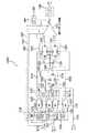
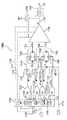
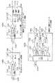
図7Aは、図6のプロセス・フローチャート600を実装するベクトル電力増幅器700の例示的な一実施形態を示すブロック図である。図7Aの例では、オプションの構成要素は、破線を用いて示されている。その他の実施形態では、さらなる構成要素を、オプションとすることができる。 FIG. 7A is a block diagram illustrating an exemplary embodiment of a
ベクトル電力増幅器700は、同相(I)ブランチ703および直交(Q)ブランチ705を含む。IブランチおよびQブランチの各々はさらに、第1のブランチおよび第2のブランチを備える。
同相(I)情報信号702は、Iデータ伝達機能モジュール(Transfer Function module)710によって受け取られる。一実施形態では、I情報信号702は、デジタル・ベースバンド信号を含む。一実施形態では、Iデータ伝達機能モジュール710は、サンプル・クロック706に従ってI情報信号702をサンプリングする。別の実施形態では、I情報信号702は、アナログ・ベースバンド信号を含み、アナログ・ベースバンド信号は、Iデータ伝達機能モジュール710に入力される前に、アナログ−デジタル変換器(ADC)(図7Aには図示されず)を使用して、デジタルに変換される。別の実施形態では、I情報信号702は、アナログ・ベースバンド信号を含み、アナログ・ベースバンド信号は、アナログ形式で、アナログ回路も含むIデータ伝達機能モジュール710に入力される。別の実施形態では、I情報信号702は、RF信号を含み、RF信号は、Iデータ伝達機能モジュール710に入力される前に、上で説明された実施形態のいずれかを使用して、ベースバンドにダウン・コンバートされる。 In-phase (I)
Iデータ伝達機能モジュール710は、I情報信号702を処理し、I情報信号702の少なくとも2つの一定包絡線構成要素信号についての同相および直交振幅情報を決定する。図5を参照して上で説明されたように、同相および直交ベクトル変調器は、それぞれsgn(I)×IUXおよびIUYに対応する振幅情報を入力する。Iデータ伝達機能モジュール710の動作は、以下のセクション3.4でさらに説明される。The I data transfer
Iデータ伝達機能モジュール710は、ベクトル変調器760および762の同相および直交振幅成分を制御するために使用される情報信号722および724を出力する。一実施形態では、信号722、724は、デジタル信号である。したがって、各信号722、724は、それぞれ対応するデジタル−アナログ変換器(DAC)730、732に供給される。DAC730、732の分解能(resolution)およびサンプル・レートは、出力信号782の所望するI成分を得るように選択される。DAC730、732は、それぞれDACクロック信号723、725によって制御される。DACクロック信号723、725は、同じクロック信号から取り出されることもでき、または独立であることもできる。 The I data transfer
別の実施形態では、信号722、724は、アナログ信号であり、DAC730、732は必要とされない。 In another embodiment, signals 722, 724 are analog signals and
図7Aの例示的な実施形態では、DAC730、732は、デジタル情報信号722、724を対応するアナログ信号に変換し、これらのアナログ信号をそれぞれオプションの補間フィルタ731、733に入力する。アンチ・エイリアス・フィルタとしても働く補間フィルタ731、733は、所望する出力波形を生成するためにDAC出力を整形する。補間フィルタ731、733は、それぞれ信号740、742を生成する。信号741は、信号740の反転を表す。信号740〜742は、ベクトル変調器760、762に入力される。 In the exemplary embodiment of FIG. 7A,
ベクトル変調器760、762は、I情報信号702の一定包絡線構成要素を生成するために、信号740〜742を適切に位相調整されたクロック信号と乗算する。クロック信号は、所望する出力信号周波数に従ったレートを有するチャネル・クロック信号708から取り出される。例えば750、752などの複数の位相スプリッタ、およびベクトル変調器乗算器(vector modulator multipliers)に関連付けられたフェーザーが、適切に位相調整されたクロック信号を生成するために使用されることができる。
図7Aの実施形態では、例えば、ベクトル変調器760は、直交振幅情報信号740を用いて、90°シフトされたチャネル・クロック信号を変調する。並行して、ベクトル変調器760は、同相振幅情報信号742を用いて、同相チャネル・クロック信号を変調する。ベクトル変調器760は、2つの変調信号を合成して、I情報信号702の第1の変調された一定包絡線構成要素761を生成する。同様に、ベクトル変調器762は、信号741および742を使用して、I情報信号702の第2の変調された一定包絡線構成要素763を生成する。信号761および763は、それぞれ、図5を参照して説明されたIU(t)およびIL(t)一定包絡線構成要素に対応する。In the embodiment of FIG. 7A, for example,
並行して同様の方法で、ベクトル電力増幅器700のQブランチは、直交(Q)情報信号704の少なくとも2つの一定包絡線構成要素信号を生成する。 In parallel, the Q branch of
図7Aの実施形態では、例えば、ベクトル変調器764は、信号744および746を使用して、Q情報信号704の第1の一定包絡線構成要素765を生成する。同様に、ベクトル変調器766は、信号745および746を使用して、Q情報信号704の第2の一定包絡線構成要素767を生成する。 In the embodiment of FIG. 7A, for example,
図5に関係して上で説明されたように、構成要素信号761、763、765、767は、実質的に等しくかつ一定の振幅の包絡線を有する。図7Aの例示的な実施形態では、信号761、763、765、767は、それぞれ対応する電力増幅器(PA)770、772、774、776に入力される。PA770、772、774、776は、線形または非線形電力増幅器とすることができる。一実施形態では、PA770、772、774、776は、スイッチング電力増幅器を含む。 As described above in connection with FIG. 5, the component signals 761, 763, 765, 767 have substantially equal and constant amplitude envelopes. In the exemplary embodiment of FIG. 7A, signals 761, 763, 765, 767 are input to corresponding power amplifiers (PA) 770, 772, 774, 776, respectively.
回路714および716(限定のためではなく参照を容易にするために、本明細書では「オートバイアス回路(autobias circuitry)」と呼ばれる)は、この実施形態では、I情報信号702およびQ情報信号704に従って、PA770、772、774、776のバイアスを制御する。図7Aの実施形態では、オートバイアス回路714および716は、それぞれバイアス信号715および717を、PA770、772およびPA774、776に提供する。オートバイアス回路714、716は、以下のセクション3.5でさらに説明される。PA770、772、774、776の実施形態も、以下のセクション3.5で説明される。
一実施形態では、PA770、772、774、776は、実質的に等しい電力増幅を、それぞれの実質的に一定の包絡線信号761、763、765、767に適用する。その他の実施形態では、追加の電力増幅を提供するために、PAドライバが追加的に利用される。図7Aの実施形態では、PAドライバ794、795、796、797は、ベクトル電力増幅器700の各ブランチの、それぞれのベクトル変調器760、762、764、766とそれぞれのPA770、772、774、776の間に任意選択で追加される。 In one embodiment,
PA770、772、774、776の出力は、ベクトル電力増幅器700の出力信号782を生成するために、一緒に結合される。一実施形態では、PA770、772、774、776の出力は、導線(wire)を使用して直接的に一緒に結合される。このような直接結合は、PA770、772、774、776の出力の間に、抵抗性、誘導性、もしくは容量性のアイソレーション(isolation)が、ごくわずか存在するだけか、または全く存在しないことを意味する。言い換えると、PA770、772、774、776の出力は、介在構成要素なしに一緒に結合される。代替として、一実施形態では、PA770、772、774、776の出力は、低いもしくは最低インピーダンス接続をもたらすインダクタンスおよび/もしくはキャパシタンスを介して、ならびに/または最小アイソレーションおよび最低電力損失をもたらす接続を介して、間接的に一緒に結合される。代替として、PA770、772、774、776の出力は、ウィルキンソン(Wilkinson)、ハイブリッド、変圧器、または知られた能動合成器など、よく知られた合成技法を使用して結合される。一実施形態では、PA770、772、774、776は、統合された増幅および電力合成を単一動作で提供する。一実施形態では、本明細書で説明される1つまたは複数の電力増幅器および/またはドライバは、複数入力、単一出力電力増幅技法を使用して実装され、その例が図7Bおよび図51A〜Hに示されている。 The outputs of
出力信号782は、I情報信号702およびQ情報信号704のIの特性およびQの特性を含む。さらに、出力信号782は、その各構成要素の周波数と同じ周波数を有し、その結果、所望するアップ・コンバートされた出力周波数を有する。ベクトル電力増幅器700の実施形態では、プルアップ・インピーダンス(pull-up impedance)780が、ベクトル増幅器700の出力と電源の間に結合される。本発明の電力増幅方法およびシステムによる出力ステージ実施形態は、以下のセクション3.5でさらに説明される。
ベクトル電力増幅器700のその他の実施形態では、増幅器の回路内のプロセス変動を補償するために、プロセス検出器が利用される。図7Aの実施形態では、例えば、プロセス検出器791〜793が、PAドライバ794〜797および位相スプリッタ750における変動を監視するために、任意選択で追加される。さらなる実施形態では、周波数変動を補償するために、周波数補償回路799が利用されることができる。 In other embodiments of the
図7Bは、ベクトル電力増幅器700の別の例示的な実施形態を示すブロック図である。オプションの構成要素は、破線を用いて示されているが、その他の実施形態では、オプションの構成要素を多くしたり少なくしたりすることができる。 FIG. 7B is a block diagram illustrating another exemplary embodiment of
この実施形態は、図7Aの増幅器の複数入力単一出力(MISO)実装を示している。図7Bの実施形態では、ベクトル変調器760、762、764、766から出力される一定包絡線信号761、763、765、767が、MISO PA784、786に入力される。MISO PA784、786は、2入力単一出力電力増幅器である。一実施形態では、MISO PA784、786は、図7Aの実施形態に示されたような要素770、772、774、776、794〜797、またはそれらの機能的同等物を含む。別の実施形態では、MISO PA784、786は、オプションのプレ・ドライバ(pre-driver)およびオプションのプロセス検出回路など、その他の要素を含むことができる。さらに、MISO PA784、786は、図7Bに示されるような2入力PAには限定されない。図51A〜Hを参照して以下でさらに説明されるその他の実施形態では、PA784、786は、任意の数の入力および出力を有することができる。 This embodiment shows a multiple input single output (MISO) implementation of the amplifier of FIG. 7A. In the embodiment of FIG. 7B, constant envelope signals 761, 763, 765, 767 output from the
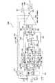
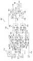
図8Aは、図6に示されたカルテシアン4ブランチVPA方法によるベクトル電力増幅器の別の例示的な実施形態800Aを示すブロック図である。オプションの構成要素は、破線を用いて示されているが、その他の実施形態は、より多いまたはより少ないオプションの構成要素を有してもよい。 FIG. 8A is a block diagram illustrating another
図8Aの実施形態では、十分な分解能およびサンプル・レートのDAC830が、図7Aの実施形態のDAC730、732、734、736に取って代わる。DAC830のサンプル・レートは、DACクロック信号826によって制御される。 In the embodiment of FIG. 8A, a sufficient resolution and
DAC830は、上で説明されたように、Iデータ伝達機能モジュール710およびQデータ伝達機能モジュール712から、それぞれ同相および直交情報信号810および820を受け取る。一実施形態では、入力セレクタ822が、DAC830に入力される信号810および820の順序を選択する。 The
DAC830は、一度に単一のアナログ信号を出力することができる。一実施形態では、図8Aに示されるように、増幅器の4つのブランチへの適切な信号タイミングを保証するために、サンプル・アンド・ホールド構成が使用されることになる。 The
DAC830は、アナログ信号832、834、836、838を、第1の組のサンプル・アンド・ホールド回路(sample-and-hold circuit)842、844、846、848に順次出力する。一実施形態では、DAC830は、図7Aの実施形態のDAC730、732、734、736の動作をエミュレートするために、十分なレートでクロックされる。出力セレクタ824は、出力信号832、834、836、838のどれが出力として選択されるべきかを決定する。 The
DAC830のDACクロック信号826、出力セレクタ信号824、入力セレクタ822、およびサンプル・アンド・ホールド・クロック840A〜D、850は、制御モジュールによって制御され、制御モジュールは、独立とすることができ、または伝達機能モジュール710および/もしくは712に統合することができる。
一実施形態では、サンプル・アンド・ホールド回路(S/H)842、844、846、848は、クロック信号840A〜Dに従って、DAC830から受け取られたアナログ値をサンプルし、ホールドする。サンプル・アンド・ホールド回路852、854、856、858は、それぞれサンプル・アンド・ホールド回路842、844、846、848からのアナログ値をサンプルし、ホールドする。次に、サンプル・アンド・ホールド回路852、854、856、858は、受け取られたアナログ値をホールドし、共通クロック信号850に従って、その値をベクトル変調器760、762、764、766に同時にリリースする。別の実施形態では、サンプル・アンド・ホールド回路852、854、856、858は、アンチ・エイリアス・フィルタでもあるオプションの補間フィルタ731、733、735、737に値をリリースする。一実施形態では、S/H852、854、856、858の出力が時間的に揃えられることを保証するために、共通クロック信号850が使用される。 In one embodiment, sample and hold circuits (S / H) 842, 844, 846, 848 sample and hold the analog value received from
ベクトル電力増幅器800Aのその他の態様は、ベクトル電力増幅器700に関係して上で説明された態様に実質的に対応する。 Other aspects of
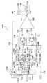
図8Bは、図6に示されたカルテシアン4ブランチVPA方法によるベクトル電力増幅器の別の例示的な実施形態800Bを示すブロック図である。オプションの構成要素は、破線を用いて示されているが、その他の実施形態は、オプションの構成要素を多くしたり少なくしたりすることができる。 FIG. 8B is a block diagram illustrating another exemplary embodiment 800B of a vector power amplifier according to the Cartesian 4-branch VPA method shown in FIG. Optional components are shown using dashed lines, but other embodiments can have more or fewer optional components.
実施形態800Bは、ベクトル電力増幅器の別の単一DAC実装を示している。しかし、図8Aの実施形態と対照すると、サンプル・アンド・ホールド構成は、サンプル・アンド・ホールド回路(S/H)の単一の組を含む。図8Bに示されるように、S/H842、844、846、848は、DAC830から、信号832、834、836、838として示されるアナログ値を受け取る。S/H回路842、844、846、848の各々は、示されるように異なるクロック840A〜Dに従って、受け取られた値をリリースする。信号740、741、742、744、745、746を生成するために使用されるアナログ・サンプルの間の時間差は、伝達機能710および712において補償されることができる。図8Bの実施形態によれば、図8Aの実施形態と比べて、S/H回路の1つのレベルが除去されることができ、それによって、増幅器のサイズおよび複雑さを減らすことができる。 Embodiment 800B shows another single DAC implementation of a vector power amplifier. However, in contrast to the embodiment of FIG. 8A, the sample and hold configuration includes a single set of sample and hold circuits (S / H). As shown in FIG. 8B, S /
ベクトル電力増幅器800Bのその他の態様は、ベクトル電力増幅器700および800Aに関係して上で説明された態様に実質的に対応する。 Other aspects of vector power amplifier 800B substantially correspond to the aspects described above with respect to
図8Cは、ベクトル電力増幅器700の別の例示的な実施形態800Cを示すブロック図である。オプションの構成要素は、破線を用いて示されているが、その他の実施形態は、オプションの構成要素を多くしたり少なくしたりすることができる。図8Cの実施形態は、図8Aの増幅器の複数入力単一出力(MISO)実装を示している。図8Cの実施形態では、ベクトル変調器760、762、764、766からの出力される一定包絡線信号761、763、765、767が、MISO PA860、862に入力される。MISO PA860、862は、2入力単一出力電力増幅器である。一実施形態では、MISO PA860、862は、図7Aの実施形態に示されたような要素770、772、774、776、794〜797、またはそれらの機能的同等物を含む。別の実施形態では、MISO PA860、862は、オプションのプレ・ドライバおよびオプションのプロセス検出回路など、その他の要素を含むことができる。別の実施形態では、MISO PA860、862は、プレ・ドライバなど、図7Aの実施形態に示されていないその他の要素を含むことができる。さらに、MISO PA860、862は、図8Cに示されるような2入力PAには限定されない。図51A〜Hを参照して以下でさらに説明されるその他の実施形態では、PA860、862は、任意の数の入力および出力を有することができる。 FIG. 8C is a block diagram illustrating another exemplary embodiment 800C of
ベクトル電力増幅器800Cのその他の態様は、ベクトル電力増幅器700および800Aに関係して上で説明された態様に実質的に対応する。 Other aspects of vector power amplifier 800C substantially correspond to the aspects described above with respect to
図8Dは、ベクトル電力増幅器700の別の例示的な実施形態800Dを示すブロック図である。オプションの構成要素は、破線を用いて示されているが、その他の実施形態は、オプションの構成要素を多くしたり少なくしたりすることができる。図8Dの実施形態は、図8Bの増幅器の複数入力単一出力(MISO)実装を示している。図8Dの実施形態では、ベクトル変調器760、762、764、766からの出力される一定包絡線信号761、763、765、767が、MISO PA870、872に入力される。MISO PA870、872は、2入力単一出力電力増幅器である。一実施形態では、MISO PA870、872は、図7Aの実施形態に示されたような要素770、772、774、776、794〜797、またはそれらの機能的同等物を含む。別の実施形態では、MISO PA870、872は、オプションのプレ・ドライバおよびオプションのプロセス検出回路など、その他の要素を含むことができる。別の実施形態では、MISO PA870、872は、プレ・ドライバなど、図7Aの実施形態に示されていないその他の要素を含むことができる。さらに、MISO PA870、872は、図8Dに示されるような2入力PAには限定されない。図51A〜Hを参照して以下でさらに説明されるその他の実施形態では、PA870および872は、任意の数の入力および出力を有することができる。 FIG. 8D is a block diagram illustrating another exemplary embodiment 800D of
ベクトル電力増幅器800Dのその他の態様は、ベクトル電力増幅器700および800Bに関係して上で説明された態様に実質的に対応する。 Other aspects of vector power amplifier 800D substantially correspond to the aspects described above with respect to
3.2)カルテシアン極カルテシアン極2ブランチ・ベクトル電力増幅器
カルテシアン極カルテシアン極(CPCP:Cartesian-Polar-Cartesian-Polar)2ブランチVPA実施形態が、今から説明される(この実施形態の名称は、限定のためではなく説明を容易にするために提供される)。3.2) Cartesian-polar Cartesian-polar two-branch vector power amplifier A Cartesian-polar-Cartesian-polar (CPCP) two-branch VPA embodiment will now be described (of this embodiment) Names are provided for ease of explanation, not limitation).
カルテシアン極カルテシアン極(CPCP)2ブランチVPA方法によれば、時間変化複素包絡線信号は、2つの実質的に一定の包絡線構成要素信号に分解される。構成要素信号は、個別に増幅され、その後、元の時間変化複素包絡線信号の増幅バージョンを構成するために合算される。加えて、時間変化複素包絡線信号の位相角が決定され、複数の構成要素信号の結果の和は、適切な角度だけシフトされた位相を有する。 According to the Cartesian pole Cartesian pole (CPCP) two-branch VPA method, the time-varying complex envelope signal is decomposed into two substantially constant envelope component signals. The component signals are amplified separately and then combined to form an amplified version of the original time-varying complex envelope signal. In addition, the phase angle of the time-varying complex envelope signal is determined, and the resulting sum of the component signals has a phase shifted by the appropriate angle.
CPCP2ブランチVPA方法の一実施形態では、時間変化複素包絡線信号の振幅および位相角は、信号の同相および直交成分から算出される。振幅情報を与えられると、2つの実質的に一定の包絡線構成要素が、所望する時間変化包絡線信号の正規化バージョンから算出され、正規化は、位相および/または振幅の実装固有の操作を含む。その後、2つの実質的に一定の包絡線構成要素は、所望する時間変化包絡線信号の位相シフトに関係する適切な角度だけ位相シフトされる。その後、実質的に一定の包絡線構成要素は、個別に実質的に等しく増幅され、元の所望する時間変化包絡線信号の増幅バージョンを生成するために合算される。 In one embodiment of the CPCP two-branch VPA method, the amplitude and phase angle of the time varying complex envelope signal are calculated from the in-phase and quadrature components of the signal. Given the amplitude information, two substantially constant envelope components are calculated from the normalized version of the desired time-varying envelope signal, which normalizes the phase and / or amplitude implementation-specific operations. Including. The two substantially constant envelope components are then phase shifted by an appropriate angle related to the phase shift of the desired time varying envelope signal. Thereafter, the substantially constant envelope components are individually substantially equally amplified and summed to produce an amplified version of the original desired time-varying envelope signal.
図9Aおよび図9Bは、フェーザー信号表現を使用して、CPCP2ブランチVPA実施形態を概念的に説明する。図9Aでは、フェーザー 9A and 9B conceptually illustrate a
は、時間変化複素包絡線入力信号r(t)を表す。任意の時刻において、Represents a time-varying complex envelope input signal r (t). At any time
は、信号r(t)の振幅および位相シフト角を反映する。図9Aに示される例では、Reflects the amplitude and phase shift angle of the signal r (t). In the example shown in FIG. 9A,
は、大きさRおよび位相シフト角θによって特徴付けられる。上で説明されたように、位相シフト角は、基準信号に対して測定される。Is characterized by a magnitude R and a phase shift angle θ. As explained above, the phase shift angle is measured relative to the reference signal.
図9Aを参照すると、 Referring to FIG. 9A,
は、Is
およびand
によって生成されるGenerated by
の相対振幅成分を表す。Represents the relative amplitude component.
図9Aを続けて参照すると、任意の時刻において、 With continued reference to FIG. 9A, at any time,
は、上側フェーザーThe upper phaser
および下側フェーザーAnd lower phaser
の合算によって獲得され得ることに留意されたい。さらに、Note that it can be obtained by adding together. further,
およびand
は、実質的に一定の大きさを有するように維持されることができる。したがって、フェーザーCan be maintained to have a substantially constant size. Therefore, phaser
およびand
は、2つの実質的に一定の包絡線信号を表す。したがって、r’(t)は、任意の時刻において、フェーザーRepresents two substantially constant envelope signals. Therefore, r '(t) is a phasor at an arbitrary time.
およびand
に対応する2つの実質的に一定の包絡線信号の合算によって獲得されることができる。Can be obtained by summing two substantially constant envelope signals corresponding to.
に対するフェーザーAgainst phasor
およびand
の位相シフトは、The phase shift of
の所望する大きさRに従って設定される。最も簡単なケースでは、上側および下側フェーザーIs set according to a desired size R. In the simplest case, upper and lower phasers
およびand
が等しい大きさをもつように選択される場合、上側および下側フェーザーUpper and lower phaser if are selected to have equal magnitude
およびand
は、Is
に対して実質的に対称的に位相シフトされる。これは、図9Aの例に示されている。「上側」および「下側」などの、ただしこれらに限定されない、向きを指示または暗示する語および句は、本明細書では参照を容易にするために使用され、機能的または構造的に限定するものではないことに留意されたい。Phase shift substantially symmetrically. This is illustrated in the example of FIG. 9A. Words and phrases that indicate or imply orientation, such as but not limited to “upper” and “lower”, are used herein for ease of reference and are functionally or structurally limited. Note that it is not a thing.
図9Aに示されるケースについて、図9Aで角 For the case shown in FIG. 9A, in FIG.
として示されるShown as
に対するAgainst
およびand
の位相シフトは、以下のように、The phase shift of
の大きさに関係付けられることが確認されることができ、Can be confirmed to be related to the size of
ここで、RはフェーザーWhere R is the phaser
の正規化された大きさを表す。Represents the normalized size of.
式(7)はさらに、 Equation (7) further
に変形されることができ、ここで、RはフェーザーWhere R is the phaser
の正規化された大きさを表す。Represents the normalized size of.
代替として、任意の実質的に等価な数学的式、またはルックアップテーブルなどその他の実質的に等価な数学的技法が、使用されることができる。 Alternatively, any substantially equivalent mathematical formula or other substantially equivalent mathematical technique such as a lookup table can be used.
上の説明から、フェーザー表現では、可変の大きさおよび位相の任意のフェーザー From the above description, the phasor representation is an arbitrary phasor of variable magnitude and phase.
は、2つの一定の大きさのフェーザー成分によって構成され得ることが導かれる。It can be derived that can be constituted by two constant size phasor components.
それに対応して、時間領域では、時間変化包絡線正弦信号r’(t)=R(t)×cos(ω)は、以下のように、2つの一定の包絡線信号によって構成され、 Correspondingly, in the time domain, the time-varying envelope sine signal r ′ (t) = R (t) × cos (ω) is composed of two constant envelope signals as follows:
ここで、Aは一定であり、Where A is constant and
は、式(7)で示されるものである。Is represented by equation (7).
図9Aから、式(9)は、
r’(t)=U’(t)+L’(t);
U’(t)=Ccos(ωt)+αsin(ωt); (10)
L’(t)=Ccos(ωt)−βsin(ωt);
と書き直され得ることがさらに確認されることができ、ここで、CはフェーザーFrom FIG. 9A, equation (9) is
r ′ (t) = U ′ (t) + L ′ (t);
U ′ (t) = C cos (ωt) + α sin (ωt); (10)
L ′ (t) = Ccos (ωt) −βsin (ωt);
Can be rewritten, where C is the phaser
およびand
の実部成分を示し、The real part component of
に等しい。Cがbe equivalent to. C is
およびand
の共通成分であることに留意されたい。αおよびβは、それぞれフェーザーNote that these are common components. α and β are phasers
およびand
の虚部成分を示し、The imaginary part component of
である。したがって、式(12)から、It is. Therefore, from equation (12):
である。当業者であれば本明細書の教示に基づいて理解されるように、例えば、ルックアップテーブルを含む、量A、B、およびCの上記表現のその他の等価および/または簡略化された表現が使用されることができる。It is. As those skilled in the art will appreciate based on the teachings herein, other equivalent and / or simplified representations of the above representations of quantities A, B, and C, including, for example, look-up tables, are available. Can be used.
はIs
に対してθ度だけシフトされていることに留意されたい。したがって、式(8)を使用して、Note that it is shifted by θ degrees relative to. Therefore, using equation (8),
であることが、演繹されることができる。Can be deduced.
式(11)は、 Equation (11) is
の表現が、θ度だけシフトされた、上で説明されたフェーザーThe expression described above is shifted by θ degrees and the phaser described above
およびand
を合算することによって獲得され得ることを含意している。さらに、It can be obtained by adding together. further,
の増幅された出力バージョンAmplified output version of
は、フェーザーThe phaser
およびand
のθ度シフト・バージョンの各々を実質的に等しく、別々に増幅し、それらを合算することによって獲得されることができる。図9Bは、この概念を示している。図9Bでは、フェーザーEach of the θ-degree shifted versions of can be obtained by substantially amplifying separately and amplifying them together. FIG. 9B illustrates this concept. In FIG. 9B, the phaser
およびand
は、フェーザーThe phaser
およびand
のθ度シフトかつ増幅バージョンを表す。Represents the θ-degree shifted and amplified version of.
およびand
は、一定の大きさのフェーザーであるので、Is a phasor of a certain size,
およびand
も、一定の大きさのフェーザーであることに留意されたい。フェーザーNote also that the phasor is of a certain size. Phaser
およびand
は合算されて、図9Bに示されるように、入力信号Are summed to obtain the input signal as shown in FIG. 9B.
の電力増幅されたバージョンであるフェーザーPhaser is a power amplified version of
になる。become.
等価的に、時間領域では、
rout(t)=U(t)+L(t);
U(t)=K[Ccos(ωt+θ)+αsin(ωt+θ)]; (12)
L(t)=K[Ccos(ωt+θ)−βsin(ωt+θ)]
と示されることができ、ここで、rout(t)は、フェーザーEquivalently, in the time domain
rout (t) = U (t) + L (t);
U (t) = K [Ccos (ωt + θ) + αsin (ωt + θ)]; (12)
L (t) = K [Ccos (ωt + θ) −βsin (ωt + θ)]
Where rout (t) is the phaser
によって表される時間領域信号に対応し、U(t)およびL(t)は、フェーザーU (t) and L (t) are phaser signals corresponding to the time domain signal represented by
およびand
によって表される時間領域信号に対応し、Kは電力増幅係数である。Where K is a power amplification factor.
式(9)および(10)の時間領域表現は正弦波形の場合について提供されたが、非正弦波形についても、適切な基底関数を使用して、等価表現が展開開発されることができることは、当業者であれば理解できよう。 Although the time domain representations of equations (9) and (10) have been provided for sinusoidal waveforms, the equivalent representation can also be developed and developed for non-sinusoidal waveforms using appropriate basis functions. Those skilled in the art will understand.
図10は、CPCP2ブランチVPA実施形態の例示的な一実施形態1000を概念的に示すブロック図である。所望する電力レベルおよび周波数特性の出力信号r(t)が、CPCP2ブランチVPA実施形態に従って、同相および直交成分から生成される。 FIG. 10 is a block diagram conceptually illustrating an
図10の例では、クロック信号1010は、出力信号r(t)を生成するための基準信号を表す。クロック信号1010は、所望する出力信号r(t)の周波数と同じ周波数を有する。 In the example of FIG. 10, the
図10を参照すると、Iclk_phase信号1012およびQclk_phase信号1014は、Clk信号1010の同相および直交成分によって乗算され、ベースバンドのIおよびQ信号化から算出された、振幅アナログ値を表す。 Referring to FIG. 10,
図10を続けて参照すると、クロック信号1010は、Iclk_phase信号1012と乗算される。並行して、クロック信号1010の90°シフト・バージョンは、Qclk_phase信号1014と乗算される。2つの乗算された信号は、合成されて、Rclk信号1016を生成する。Rclk信号1016は、クロック信号1010と同じ周波数を有する。さらに、Rclk信号1016は、Q(t)とI(t)の比に従う位相シフト角によって特徴付けられる。Rclk信号1016の大きさは、R2clk=I2clk_phase+Q2clk_phaseのようになる。したがって、Rclk信号1016は、所望する出力信号r(t)の位相特性を有する実質的に一定の包絡線信号を表す。With continued reference to FIG. 10, the
図10を続けて参照すると、Rclk信号1016は、並列して、2つのベクトル変調器1060および1062に入力される。ベクトル変調器1060および1062は、それぞれ、(12)に記述されるような、所望する出力信号r(t)の実質的に一定の包絡線構成要素U(t)およびL(t)を生成する。ベクトル変調器1060では、共通信号1028と乗算された同相Rclk信号1020が、第1の信号1026と乗算された、Rclk信号の90°シフト・バージョン1018と合成される。並行して、ベクトル変調器1062では、共通信号1028と乗算された同相Rclk信号1022が、第2の信号1030と乗算された、Rclk信号の90°シフト・バージョン1024と合成される。共通信号1028、第1の信号1026、および第2の信号1030は、それぞれ、式(12)に記述されるような、実部C、ならびに虚部αおよびβに対応する。 With continued reference to FIG. 10, the
それぞれのベクトル変調器1060および1062の出力信号1040および1042は、それぞれ、入力信号r(t)の実質的に一定の包絡線構成要素U(t)およびL(t)に対応する。 The output signals 1040 and 1042 of the
上で説明されたように、信号1040および1042は、実質的に等しくかつ一定の振幅の包絡線を有することによって特徴付けられる。したがって、信号1040および1042が、対応する電力増幅器(PA)1044および1046に入力される場合、対応する増幅された信号1048および1050は、実質的に一定の包絡線信号である。 As explained above, signals 1040 and 1042 are characterized by having substantially equal and constant amplitude envelopes. Thus, when signals 1040 and 1042 are input to corresponding power amplifiers (PA) 1044 and 1046, the corresponding amplified
電力増幅器1044および1046は、実質的に等しい電力増幅を、それぞれ信号1040および1042に適用する。一実施形態では、PA1044および1046の電力増幅レベルは、出力信号r(t)の所望する出力レベルに従って設定される。さらに、増幅された信号1048および1050は、互いに対して同相である。したがって、図10に示されるように、一緒に合算されるとき、結果の信号1052は、所望する出力信号r(t)に対応する。
図10Aは、CPCP2ブランチVPA実施形態の別の例示的な実施形態1000Aである。実施形態1000Aは、図10の実施形態1000の複数入力単一出力(MISO)実装を表す。 FIG. 10A is another
実施形態1000Aでは、ベクトル変調器1060および1062から出力される一定包絡線信号1040および1042は、MISO PA1054に入力される。MISO PA1054は、2入力単一出力増幅器である。一実施形態では、MISO PA1054は、例えば、プレ・ドライバ、ドライバ、電力増幅器、およびプロセス検出器など(図10Aには図示されず)、様々な要素を含むことができる。さらに、MISO PA1054は、図10Aに示されるような、2入力PAに限定されない。図51A〜Hを参照して以下でさらに説明されるその他の実施形態では、PA1054は、任意の数の入力を有することができる。 In
CPCP2ブランチVPA実施形態の動作が、図11のプロセス・フローチャート1100に示されている。 The operation of the CPCP 2-branch VPA embodiment is illustrated in the
プロセスは、所望する出力信号のベースバンド表現を受け取ることを含むステップ1110で開始する。一実施形態では、これは、所望する出力信号の同相(I)および直交(Q)成分を受け取ることを含む。別の実施形態では、これは、所望する出力信号の振幅および位相を受け取ることを含む。 The process begins at
ステップ1120は、所望する出力信号の所望する出力信号周波数に従って設定されるクロック信号を受け取ることを含む。図10の例では、ステップ1120は、クロック信号1010を受け取ることによって達成される。
ステップ1130は、クロック信号を処理して、受け取られたI成分およびQ成分に従う位相シフト角度を有する正規化クロック信号を生成することを含む。一実施形態では、正規化クロック信号は、I成分およびQ成分の比に従う位相シフト角度を有する一定包絡線信号である。正規化信号の位相シフト角度は、元のクロック信号に対するものである。図10の例では、ステップ1130は、クロック信号1010の同相および直交成分を、Iclk_phase信号1012およびQclk_phase信号1014で乗算し、その後、Rclk信号1016を生成するために乗算された信号を合算することによって達成される。
ステップ1140は、I成分およびQ成分の処理を含み、第1および第2の実質的に一定の包絡線構成要素信号を生成するのに必要な振幅情報を生成する。
ステップ1150は、ステップ1140の振幅情報および正規化クロック信号Rclkを処理して、所望する出力信号の第1および第2の一定包絡線構成要素信号を生成することを含む。一実施形態では、ステップ1150は、所望する出力信号の第1および第2の一定包絡線構成要素を、正規化クロック信号の位相シフト角だけ位相シフトすることを含む。図10の例では、ステップ1150は、Rclk信号1016を第1の信号1026、第2の信号1030、および共通信号1028で変調して、信号1040および1042を生成する、ベクトル変調器1060および1062によって達成される。
ステップ1160は、第1および第2の一定包絡線構成要素を個別に増幅し、増幅された信号を合算し、所望する出力信号を生成することを含む。一実施形態では、第1および第2の一定包絡線構成要素の増幅は、実質的に等しく、所望する出力信号の所望する電力レベルに基づいている。図10の例では、ステップ1160は、信号1040および1042を増幅して、増幅された信号1048および1050を生成する、PA1044および1046によって達成される。
図12は、プロセス・フローチャート1100を実装するベクトル電力増幅器1200の例示的な一実施形態を示すブロック図である。オプションの構成要素は、破線を用いて示されているが、その他の実施形態では、より多いまたはより少ない構成要素を、オプションとすることができる。 FIG. 12 is a block diagram illustrating an exemplary embodiment of a
図12を参照すると、同相(I)および直交(Q)情報信号1210が、IおよびQのデータ伝達機能モジュール1216によって受け取られる。一実施形態では、IおよびQのデータ伝達機能モジュール1216は、サンプル・クロック1212に従って信号1210をサンプリングする。IおよびQの情報信号1210は、所望する出力信号r(t)のベースバンドIおよびQの情報を含む。 Referring to FIG. 12, in-phase (I) and quadrature (Q) information signals 1210 are received by I and Q data
一実施形態では、IおよびQのデータ伝達機能モジュール1216は、信号1210を処理して、情報信号1220、1222、1224、1226を生成する。IおよびQのデータ伝達機能モジュール1216の動作は、以下のセクション3.4でさらに説明される。 In one embodiment, I and Q data
図12を参照すると、情報信号1220は、所望する出力信号r(t)のベースバンド・バージョンの第1および第2の一定包絡線構成要素の直交振幅情報を含む。例えば、図9Aを参照すると、情報信号1220は、αおよびβ直交成分を含む。図12を参照すると、情報信号1226は、信号r(t)のベースバンド・バージョンの第1および第2の一定包絡線構成要素の同相振幅情報を含む。例えば、図9Aを参照すると、情報信号1226は、共通C同相成分を含む。 Referring to FIG. 12,
図12を続けて参照すると、情報信号1222および1224は、それぞれ正規化された同相Iclk_phaseおよび直交Qclk_phase信号を含む。Iclk_phaseおよびQclk_phaseは、信号1210に含まれるIおよびQの情報信号の正規化バージョンである。一実施形態では、Iclk_phaseおよびQclk_phaseは、(I2clk_phase+Q2clk_phase=定数)となるように正規化される。信号1250の位相は、所望する出力信号の位相に対応し、Iclk_phaseおよびQclk_phaseから生成されることに留意されたい。図9Bを参照すると、Iclk_phaseおよびQclk_phaseは、以下のように、IおよびQに関係付けられ、With continued reference to FIG. 12, information signals 1222 and 1224 include normalized in-phase Iclk_phase and quadrature Qclk_phase signals, respectively. Iclk_phase and Qclk_phase are normalized versions of the I and Q information signals included in
ここで、θは、図9BでフェーザーWhere θ is the phasor in FIG. 9B
によって表される、所望する出力信号の位相を表す。ベースバンドIおよびQの情報の符号情報は、4つの象限すべてについてθを算出するために考慮されなければならない。Represents the phase of the desired output signal, represented by The sign information of the baseband I and Q information must be taken into account to calculate θ for all four quadrants.
図12の例示的な実施形態では、情報信号1220、1222、1224、1226は、デジタル信号である。したがって、情報信号1220、1222、1224、1226の各々は、対応するデジタル−アナログ変換器(DAC)1230、1232、1234、1236に供給される。DAC1230、1232、1234、1236の分解能およびサンプル・レートは、特定の信号方式(specific signaling schemes)に従って選択される。DAC1230、1232、1234、1236は、それぞれDACクロック信号1221、1223、1225、1227によって制御される。DACクロック信号1221、1223、1225、1227は、同じクロック信号から取り出されることもでき、または独立であることもできる。 In the exemplary embodiment of FIG. 12, the information signals 1220, 1222, 1224, 1226 are digital signals. Accordingly, each of the information signals 1220, 1222, 1224, 1226 is provided to a corresponding digital-to-analog converter (DAC) 1230, 1232, 1234, 1236. The resolution and sample rate of the
他の実施形態では、情報信号1220、1222、1224、1226は、アナログ形式で生成され、DACは必要とされない。 In other embodiments, the information signals 1220, 1222, 1224, 1226 are generated in analog form and no DAC is required.
図12を参照すると、DAC1230、1232、1234、1236は、デジタル情報信号1220、1222、1224、1226を対応するアナログ信号に変換し、これらのアナログ信号をそれぞれオプションの補間フィルタ1231、1233、1235、1237に入力する。アンチ・エイリアス・フィルタとしても働く補間フィルタ1231、1233、1235、1237は、所望する出力波形を生成するためにDAC出力信号を整形する。補間フィルタ1231、1233、1235、1237は、それぞれ信号1240、1244、1246、1248を生成する。信号1242は、信号1240の反転を表す。 Referring to FIG. 12,
図12を続けて参照すると、Iclk_phaseおよびQclk_phase情報を含む信号1244および1246が、ベクトル変調器1238に入力される。ベクトル変調器1238は、信号1244をチャネル・クロック信号1214で乗算する。チャネル・クロック信号1214は、所望する出力信号周波数に従って選択される。並行して、ベクトル変調器1238は、信号1246をチャネル・クロック信号1214の90°シフト・バージョンで乗算する。言い換えると、ベクトル変調器1238は、Iclk_phaseの振幅を有する同相成分およびQclk_phaseの振幅を有する直交成分を生成する。 With continued reference to FIG. 12,
ベクトル変調器1238は、2つの変調信号を合成して、Rclk信号1250を生成する。Rclk信号1250は、所望する出力周波数、および信号1210に含まれるIおよびQのデータに従う位相シフト角、を有する実質的に一定の包絡線信号である。
図12を続けて参照すると、信号1240、1242、1248は、それぞれ信号r(t)の複素包絡線のU、L、および共通C振幅成分を含む。信号1240、1242、1248は、Rclk信号1250とともに、ベクトル変調器1260および1262に入力される。 With continued reference to FIG. 12,
ベクトル変調器1260は、Rclk信号1250の90°シフト・バージョンと乗算された信号1240と、Rclk信号1250の0°シフト・バージョンと乗算された信号1248とを合算して、出力信号1264を生成する。並行して、ベクトル変調器1262は、Rclk信号1250の90°シフト・バージョンと乗算された信号1242と、Rclk信号1250の0°シフト・バージョンと乗算された信号1248とを合算して、出力信号1266を生成する。
出力信号1264および1266は、実質的に一定の包絡線信号を表す。さらに、Rclk信号1250に対する出力信号1264および1266の位相シフトは、それぞれ比α/Cおよびβ/Cに関連付けられた角度関係によって決定される。一実施形態では、α=−βであり、したがって、出力信号1264および1266は、Rclk信号1250に対して対称的に位相調整されている。例えば、図9Bを参照すると、出力信号1264および1266は、それぞれ一定の大きさのフェーザー
およびand
に対応する。Corresponding to
出力信号1264および1266の和が、ベースバンド信号r(t)のIおよびQの特性を有するチャネル・クロック変調信号(channel-clock-modulated signal)をもたらす。しかし、ベクトル変調器1200の出力で所望する電力レベルを達成するため、信号1264および1266は、増幅されて、増幅された出力信号を生成する。図12の実施形態では、信号1264および1266は、それぞれ電力増幅器(PA)1270および1272に入力され、増幅される。一実施形態では、PA1270および1272は、スイッチング電力増幅器を含む。オートバイアス回路1218は、以下のセクション3.5.2でさらに説明されるように、PA1270および1272のバイアスを制御する。図12の実施形態では、例えば、オートバイアス回路1218は、PA1270および1272にバイアス電圧1228を提供する。 The sum of
一実施形態では、PA1270および1272は、それぞれの一定包絡線信号1264〜1266に、実質的に等しい電力増幅を適用する。一実施形態では、電力増幅は、所望する出力電力レベルに従って設定される。ベクトル電力変調器1200のその他の実施形態では、追加の電力増幅能力を増幅器に提供するために、PAドライバおよび/またはプレ・ドライバが追加的に利用される。図12の実施形態では、例えば、PAドライバ1284および1286が、それぞれベクトル変調器1260および1262と後続のPA1270および1272の間に任意選択で追加される。 In one embodiment,
PA1270および1272のそれぞれ出力信号1274および1276は、実質的に一定の包絡線信号である。さらに、出力信号1274および1276が合算されるとき、結果として得られる信号は、最小の非線形歪みを有する。図12の実施形態では、出力信号1274および1276は、ベクトル電力増幅器1200の出力信号1280を生成するために一緒に結合される。一実施形態では、PA1270および1272の出力を結合する際にアイソレーションは使用されない。したがって、結合によって受けるのは最小電力損失に過ぎない。一実施形態では、PA1270および1272の出力は、導線を使用して直接的に一緒に結合される。このような直接結合は、PA1270および1272の出力の間に、抵抗性、誘導性、もしくは容量性のアイソレーションがごくわずか存在するだけか、またはまったく存在しないことを意味する。言い換えると、PA1270および1272の出力は、介在構成要素なしに一緒に結合される。代替として、一実施形態では、PA1270および1272の出力は、低いもしくは最低インピーダンス接続をもたらすインダクタンスおよび/もしくはキャパシタンスを介して、ならびに/または最小アイソレーションおよび最低電力損失をもたらす接続を介して、間接的に一緒に結合される。代替として、PA1270および1272の出力は、ウィルキンソン、ハイブリッド合成器、変圧器、または知られた能動合成器など、よく知られた合成技法を使用して結合される。一実施形態では、PA1270および1272は、統合された増幅および電力合成を単一動作で提供する。一実施形態では、本明細書で説明される1つまたは複数の電力増幅器および/またはドライバは、複数入力単一出力電力増幅技法を使用して実装され、その例が、図12A、図12Bおよび図51A〜Hに示されている。 The output signals 1274 and 1276 of
出力信号1280は、ベースバンド信号r(t)のIおよびQの特性、ならびに所望する出力電力レベルおよび周波数、を有する信号を表す。ベクトル電力増幅器1200の実施形態では、プルアップ・インピーダンス1288が、ベクトル電力増幅器1200の出力と電源の間に結合される。その他の実施形態では、インピーダンス整合ネットワーク1290が、ベクトル電力増幅器1200の出力において結合される。本発明の電力増幅方法およびシステムによる出力ステージ実施形態は、以下のセクション3.5でさらに説明される。
ベクトル電力増幅器1200のその他の実施形態では、増幅器の回路内のプロセス変動を補償するために、プロセス検出器が利用される。図12の例示的な実施形態では、例えば、プロセス検出器1282が、PAドライバ1284および1286における変動を監視するために、任意選択で追加される。 In other embodiments of the
図12Aは、プロセス・フローチャート1100を実装するベクトル電力増幅器1200Aの別の例示的な実施形態を示すブロック図である。オプションの構成要素は、破線を用いて示されているが、その他の実施形態では、より多いまたはより少ない構成要素を、オプションとすることができる。 FIG. 12A is a block diagram illustrating another exemplary embodiment of a
実施形態1200Aは、実施形態1200の複数入力単一出力(MISO)実装を示している。実施形態1200Aでは、ベクトル変調器1260および1262から出力される一定包絡線信号1261および1263は、MISO PA1292に入力される。MISO PA1292は、2入力単一出力電力増幅器である。一実施形態では、MISO PA1292は、図12の実施形態に示されるような要素1270、1272、1282、1284、1286を含む。別の実施形態では、MISO PA1292は、プレ・ドライバなど、図12の実施形態に示されていないその他の要素を含むことができる。さらに、MISO PA1292は、図12Aに示されるような2入力PAには限定されない。図51A〜Hを参照して以下でさらに説明されるその他の実施形態では、PA1292は、任意の数の入力および出力を有することができる。
図12Aを続けて参照すると、実施形態1200Aは、オートバイアス信号をMISO PA1292に送るための一実装を示している。図12Aの実施形態では、オートバイアス回路1218によって生成されるオートバイアス信号1288は、MISO PA1292の異なるステージにバイアスをかけるために、それから1つまたは複数の信号を引き出される。図12Aの例に示されるように、3つのバイアス制御信号Bias A、Bias B、Bias Cが、オートバイアス信号1288から引き出され、その後、MISO PA1292の異なるステージに入力される。例えば、Bias Cは、MISO PA1292のプレ・ドライバ・ステージへのバイアス信号とすることができる。同様に、Bias BおよびBias Aは、MISO PA1292のドライバおよびPAステージへのバイアス信号とすることができる。 With continued reference to FIG. 12A,
図12Bの実施形態1200Bに示される別の実装では、オートバイアス回路1218は、それぞれBias A、Bias B、Bias Cに対応する別々のオートバイアス信号1295、1296、1295を生成する。信号1295、1296、1297は、オートバイアス回路1218内で別々に生成されてもよく、または別々に生成されなくてもよいが、示されるように別々に出力される。さらに、信号1295、1296、1297は、MISO PA1294の異なるステージのバイアシングによって決定されるように関係付けられてもよく、または関係付けられなくてもよい。 In another implementation shown in embodiment 1200B of FIG. 12B, the auto-
ベクトル電力増幅器1200Aおよび1200Bのその他の態様は、ベクトル電力増幅器1200に関係して上で説明された態様に実質的に対応する。 Other aspects of
図13は、CPCP2ブランチVPA実施形態によるベクトル電力増幅器の別の例示的な実施形態1300を示すブロック図である。オプションの構成要素は、破線を用いて示されているが、その他の実施形態では、より多いまたはより少ない構成要素を、オプションとすることができる。 FIG. 13 is a block diagram illustrating another
図13の例示的な実施形態では、十分な分解能およびサンプル・レートのDAC1320が、図12の実施形態のDAC1230、1232、1234、1236に取って代わる。DAC1320は、DACクロック信号1324によって制御される。 In the exemplary embodiment of FIG. 13, a sufficient resolution and sample rate DAC 1320 replaces the
DAC1320は、IおよびQのデータ伝達機能モジュール1216から、情報信号1310を受け取る。情報信号1310は、図12の実施形態の信号1220、1222、1224、1226と同一の情報内容を含む。 The DAC 1320 receives the information signal 1310 from the I and Q data
DAC1320は、一度に単一のアナログ信号を出力することができる。したがって、図13に示されるように、サンプル・アンド・ホールド構成が使用されることになる。 The DAC 1320 can output a single analog signal at a time. Therefore, a sample and hold configuration will be used as shown in FIG.
DAC1320は、アナログ信号1332、1334、1336、1336を、第1の組のサンプル・アンド・ホールド回路1342、1344、1346、1348に順次出力する。一実施形態では、DAC1320は、図12の実施形態のDAC1230、1232、1234、1236に取って代わるために、十分なレートでクロックされる。出力セレクタ1322は、出力信号1332、1334、1336、1338のどれが出力として選択されるべきかを決定する。 The DAC 1320 sequentially outputs the
DAC1320のDACクロック信号1324、出力セレクタ信号1322、およびサンプル・アンド・ホールド・クロック1340A〜D、1350は、制御モジュールによって制御され、制御モジュールは、独立とすることができ、または伝達機能モジュール1216に統合することができる。 The DAC clock signal 1324, the output selector signal 1322, and the sample and hold clocks 1340A-D, 1350 of the DAC 1320 are controlled by the control module, which can be independent or to the
一実施形態では、サンプル・アンド・ホールド回路(S/H)1342、1344、1346、1348は、受け取られたアナログ値をホールドし、クロック信号1340A〜Dに従って、その値を第2の組のサンプル・アンド・ホールド回路1352、1354、1356、1358にリリースする。例えば、S/H1342は、受け取られたクロック信号1340Aに従って、その値をS/H1352にリリースする。次に、サンプル・アンド・ホールド回路1352、1354、1356、1358は、受け取られたアナログ値をホールドし、共通クロック信号1350に従って、その値を補間フィルタ1231、1233、1235、1237に同時にリリースする。共通クロック信号1350は、S/H1352、1354、1356、1358の出力が時間的に揃えられることを保証するために使用される。 In one embodiment, sample and hold circuits (S / H) 1342, 1344, 1346, 1348 hold the received analog values and, according to clock signals 1340A-D, store the values in a second set of samples. Release to the AND
別の実施形態では、S/H1342、1344、1346、1348を含む単一の層のS/H回路が利用されることができる。したがって、S/H回路1342、1344、1346、1348は、DAC1320からアナログ値を受け取り、各回路は、その受け取られた値を他から独立のクロックに従ってリリースする。例えば、S/H1342は、S/H1344を制御するクロック1340Bと同期しなくてもよいクロック1340Aによって制御される。S/H回路1342、1344、1346、1348の出力が時間的に揃えられることを保証するため、クロック1340A〜Dの間の遅延は、増幅器の前のステージにおいて事前補償される。例えば、DAC1320は、クロック1340A〜Dの間の時間差を補償するために、適切に選択された遅延を有する信号1332、1334、1336、1338を、S/H回路1342、1344、1346、1348に出力する。 In another embodiment, a single layer S / H circuit including S / H 1342, 1344, 1346, 1348 may be utilized. Thus, the S / H circuits 1342, 1344, 1346, 1348 receive analog values from the DAC 1320, and each circuit releases the received values according to a clock independent of the others. For example, the S / H 1342 is controlled by a clock 1340A that may not be synchronized with the clock 1340B that controls the S / H 1344. To ensure that the outputs of S / H circuits 1342, 1344, 1346, 1348 are time aligned, the delay between clocks 1340A-D is precompensated in the previous stage of the amplifier. For example, DAC 1320 outputs signals 1332, 1334, 1336, 1338 with appropriately selected delays to S / H circuits 1342, 1344, 1346, 1348 to compensate for the time difference between clocks 1340A-D. To do.
ベクトル電力増幅器1300のその他の態様は、ベクトル電力増幅器1200に関係して上で説明された態様と実質的に等価である。 Other aspects of the
図13Aは、CPCP2ブランチVPA実施形態によるベクトル電力増幅器の別の例示的な実施形態1300Aを示すブロック図である。オプションの構成要素は、破線を用いて示されているが、その他の実施形態では、より多いまたはより少ない構成要素を、オプションとすることができる。実施形態1300Aは、図13の実施形態1300のMISO実装である。 FIG. 13A is a block diagram illustrating another
図13Aの実施形態では、ベクトル変調器1260および1262から出力される一定包絡線信号1261および1263は、MISO PA1360に入力される。MISO PA1360は、2入力単一出力電力増幅器である。一実施形態では、MISO PA1360は、図13の実施形態に示されるような要素1270、1272、1282、1284、1286を含む。別の実施形態では、MISO PA1360は、プレ・ドライバなど、図13の実施形態に示されていないその他の要素、またはそれらの機能的同等物を含むことができる。さらに、MISO PA1360は、図13Aに示されるような2入力PAには限定されない。図51A〜Hを参照して以下でさらに説明されるその他の実施形態では、PA1360は、任意の数の入力を有することができる。 In the embodiment of FIG. 13A,
図13Aの実施形態はさらに、示されるように単一または2つのレベルのS/H回路を有する2つの異なるサンプル・アンド・ホールド構成を示している。2つの実装は、図13に関係して上で説明された。 The embodiment of FIG. 13A further illustrates two different sample and hold configurations with single or two level S / H circuits as shown. Two implementations have been described above in connection with FIG.
実施形態1300Aは、オプションのバイアス制御回路1218および関連バイアス制御信号1325、1326、1327も示している。信号1325、1326、1327は、ある種の実施形態においてMISO PA1360の個々の異なるステージにバイアスをかけるために使用されることができる。
ベクトル電力増幅器1300Aのその他の態様は、ベクトル電力増幅器1200および1300に関係して上で説明された態様と等価である。 Other aspects of
3.3)直接カルテシアン2ブランチ・ベクトル電力増幅器
直接カルテシアン2ブランチ(Direct Cartesian 2-Branch)VPA実施形態が、今から説明される。この名称は、本明細書では参照目的で使用され、機能的または構造的に限定するものではない。3.3) Direct Cartesian 2-Branch Vector Power Amplifier A Direct Cartesian 2-Branch VPA embodiment will now be described. This name is used herein for reference purposes and is not functionally or structurally limited.
直接カルテシアン2ブランチVPA実施形態によれば、時間変化包絡線信号は、2つの一定包絡線構成要素信号に分解される。構成要素信号は、個別に等しくまたは実質的に等しく増幅され、その後、元の時間変化包絡線信号の増幅バージョンを構成するために合算される。 According to the direct Cartesian two-branch VPA embodiment, the time varying envelope signal is decomposed into two constant envelope component signals. The component signals are amplified individually or substantially equally and then combined to form an amplified version of the original time-varying envelope signal.
直接カルテシアン2ブランチVPA実施形態の一実施形態では、時間変化包絡線信号の振幅および位相角は、入力信号の同相および直交成分から算出される。振幅および位相情報を使用して、時間変化包絡線信号の2つの一定包絡線構成要素用の同相および直交振幅成分が、算出される。その後、2つの一定包絡線構成要素が生成され、等しくまたは実質的に等しく増幅され、元の時間変化包絡線信号Rinの増幅バージョンを生成するために合算される。In one embodiment of the direct Cartesian 2-branch VPA embodiment, the amplitude and phase angle of the time varying envelope signal are calculated from the in-phase and quadrature components of the input signal. Using the amplitude and phase information, the in-phase and quadrature amplitude components for the two constant envelope components of the time-varying envelope signal are calculated. Thereafter, two constant envelope components are generated, amplified equally or substantially equally, and combined to produce an amplified version of the original time-varying envelope signal Rin .
直接カルテシアン2ブランチVPAの概念が、図9Aおよび図14を参照して今から説明される。 The concept of direct Cartesian two-branch VPA will now be described with reference to FIGS. 9A and 14.
図9Aに関係して説明され確認されたように、フェーザー As described and confirmed in connection with FIG.
は、Is
を生成するために適切に位相調整された、上側フェーザーUpper phaser, properly phased to produce
および下側フェーザーAnd lower phaser
の合算によって獲得されることができる。Can be obtained by adding together.
は、大きさRinに比例するように算出される。さらに、Is calculated to be proportional to the magnitude Rin . further,
およびand
は、実質的に一定の大きさを有するように維持されることができる。時間領域では、Can be maintained to have a substantially constant size. In the time domain,
およびand
は、2つの実質的に一定の包絡線信号を表す。したがって、Represents two substantially constant envelope signals. Therefore,
の時間領域同等物r’(t)は、任意の時刻において、2つの実質的に一定の包絡線信号の合算によって獲得されることができる。The time domain equivalent r '(t) can be obtained at any given time by the sum of two substantially constant envelope signals.
図9Aに示されたケースの場合、図9Aで角 In the case of the case shown in FIG.
として示された、Shown as
に対するAgainst
およびand
の位相シフトは、以下のように、The phase shift of
の大きさに関係付けられ、Is related to the size of
ここで、Rは、フェーザーWhere R is the phaser
の正規化された大きさを表す。Represents the normalized size of.
時間領域では、時間変化包絡線信号、例えば、r’(t)=R(t)cos(ωt)は、以下のように、2つの一定包絡線信号の和によって構成されることができ、
r’(t)=U’(t)+L’(t);
U’(t)=C×cos(ωt)+α×sin(ωt); (14)
L’(t)=C×cos(ωt)−β×sin(ωt);
ここで、CはフェーザーIn the time domain, a time-varying envelope signal, eg, r ′ (t) = R (t) cos (ωt), can be composed of the sum of two constant envelope signals as follows:
r ′ (t) = U ′ (t) + L ′ (t);
U ′ (t) = C × cos (ωt) + α × sin (ωt); (14)
L ′ (t) = C × cos (ωt) −β × sin (ωt);
Where C is the phaser
およびand
の同相振幅成分を示し、Shows the in-phase amplitude component of
に等しいか、または実質的に等しい(Aは一定)。αおよびβは、それぞれフェーザーOr substantially equal (A is constant). α and β are phasers
およびand
の直交振幅成分を示す。The quadrature amplitude component is shown.
である。式(14)は、基底関数を正弦関数から所望する関数に変更することによって、非正弦信号用に変更することができることに留意されたい。It is. Note that equation (14) can be modified for non-sinusoidal signals by changing the basis function from a sine function to the desired function.
図14は、フェーザー Figure 14 shows the phaser
ならびにその2つの一定の大きさの構成要素フェーザーAnd its two constant sized component phasers
およびand
を示している。Is shown.
は、図9AにおけるIn FIG. 9A
に対してθ度だけシフトされている。したがって、Is shifted by θ degrees. Therefore,
であることが確認されることができる。It can be confirmed that
式(15)から、 From equation (15)
であることがさらに示されることができる。It can be further shown that:
同様に、 Similarly,
であることが示されることができる。Can be shown to be.
式(16)および(17)は、 Equations (16) and (17) are
と書き直されることができる。And can be rewritten.
等価的に、時間領域では、
U(t)=Uxφ1(t)+Uyφ2(t);
L(t)=Lxφ1(t)+Lyφ2(t); (19)
であり、ここで、φ1(t)およびφ2(t)は、適切に選択された直交基底関数を表す。Equivalently, in the time domain
U (t) = Ux φ1 (t) + Uy φ2 (t);
L (t) = Lx φ1 (t) + Ly φ2 (t); (19)
Where φ1 (t) and φ2 (t) represent appropriately selected orthogonal basis functions.
式(18)および(19)から、時間変化包絡線信号r(t)の2つの一定包絡線構成要素を決定するには、α、β、C、ならびにsin(Θ)およびcos(Θ)の値を算出すれば十分であることが知られる。さらに、α、β、およびCは、信号r(t)の振幅および位相情報から、等価的にIおよびQの成分から、完全に決定されることができる。 From equations (18) and (19), to determine the two constant envelope components of the time-varying envelope signal r (t), α, β, C, and sin (Θ) and cos (Θ) It is known that calculating the value is sufficient. Furthermore, α, β, and C can be completely determined from the amplitude and phase information of the signal r (t), equivalently from the I and Q components.
図15は、直接カルテシアン2ブランチVPA実施形態の例示的な一実施形態1500を概念的に示すブロック図である。所望する電力レベルおよび周波数特性の出力信号r(t)が、直接カルテシアン2ブランチVPA実施形態に従って同相および直交成分から生成される。 FIG. 15 is a block diagram conceptually illustrating an
図15の実施形態では、クロック信号1510は、出力信号r(t)を生成するための基準信号を表す。クロック信号1510は、所望する出力信号r(t)の周波数と同じ周波数を有する。 In the embodiment of FIG. 15,
図15を参照すると、例示的な実施形態1500は、第1のブランチ1572および第2のブランチ1574を含む。第1のブランチ1572は、ベクトル変調器1520および電力増幅器(PA)1550を含む。同様に、第2のブランチ1574は、ベクトル変調器1530および電力増幅器(PA)1560を含む。 With reference to FIG. 15, an
図15を続けて参照すると、クロック信号1510が、ベクトル変調器1520および1530に並行して入力される。ベクトル変調器1520では、Ux信号1526と乗算されたクロック信号1510の同相バージョン1522が、Uy信号1528と乗算されたクロック信号1510の90°シフト・バージョン1524と合算される。並行して、ベクトル変調器1530では、Lx信号1536と乗算されたクロック信号1510の同相バージョン1532が、Ly信号1538と乗算されたクロック信号1510の90°シフト・バージョン1534と合算される。Ux信号1526およびUy信号1528は、それぞれ、式(19)で提供される、信号r(t)の一定包絡線構成要素分U(t)の同相および直交振幅成分に対応する。同様に、Lx信号1536およびLy信号1538は、それぞれ、式(19)で提供される、信号r(t)の一定包絡線構成要素L(t)の同相および直交振幅成分に対応する。With continued reference to FIG. 15,
したがって、ベクトル変調器1520および1530のそれぞれの出力信号1540および1542は、上の式(19)に記されたように、それぞれ信号r(t)の一定包絡線構成要素U(t)およびL(t)に対応する。上で説明されたように、信号1540および1542は、等しくかつ一定のまたは実質的に等しくかつ一定の振幅の包絡線を有することによって特徴付けられる。 Accordingly, the
図15を参照すると、所望する電力レベルの出力信号r(t)を生成するため、信号1540および1542が、対応する電力増幅器1550および1560に入力される。 Referring to FIG. 15,
一実施形態では、電力増幅器1550および1560は、等しいまたは実質的に等しい電力増幅を、それぞれ信号1540および1542に適用する。一実施形態では、PA1550および1560の電力増幅は、出力信号r(t)の所望する電力レベルに従って設定される。 In one embodiment,
増幅出力信号1562および1564は、実質的に一定の包絡線信号である。したがって、図15に示されるように、一緒に合算された場合、結果の信号1570は、所望する出力信号r(t)に対応する。 Amplified
図15Aは、直接カルテシアン2ブランチVPA実施形態の別の例示的な実施形態1500Aである。実施形態1500Aは、図15の実施形態1500の複数入力単一出力(MISO)実装を表す。 FIG. 15A is another
実施形態1500Aでは、ベクトル変調器1520および1530から出力される一定包絡線信号1540および1542は、MISO PA1580に入力される。MISO PA1580は、2入力単一出力増幅器である。一実施形態では、MISO PA1580は、例えば、プレ・ドライバ、ドライバ、電力増幅器、およびプロセス検出器など(図15Aには図示されず)、様々な要素を含むことができる。さらに、MISO PA1580は、図15Aに示されるような、2入力PAに限定されない。図51A〜Hを参照して以下でさらに説明されるその他の実施形態では、PA1580は、任意の数の入力を有することができる。 In
直接カルテシアン2ブランチVPA実施形態の動作が、図16のプロセス・フローチャート1600に示されている。プロセスは、所望する出力信号のベースバンド表現を受け取ることを含むステップ1610で開始する。一実施形態では、ベースバンド表現は、IおよびQの成分を含む。別の実施形態では、IおよびQの成分は、ベースバンドにダウン・コンバートされるRF成分である。 The operation of the direct Cartesian two-branch VPA embodiment is illustrated in the
ステップ1620は、所望する出力信号の所望する出力信号周波数に従って設定されるクロック信号を受け取ることを含む。図15の例では、ステップ1620は、クロック信号1510を受け取ることによって達成される。
ステップ1630は、所望する出力信号の第1および第2の一定包絡線構成要素信号の同相および直交振幅情報を生成するためにIおよびQの成分を処理することを含む。図15の例では、同相および直交振幅情報は、Ux、Uy、Lx、およびLyによって示されている。
ステップ1640は、所望する出力信号の第1および第2の一定包絡線構成要素信号を生成するために振幅情報およびクロック信号を処理することを含む。一実施形態では、第1および第2の一定包絡線構成要素信号は、所望する出力信号周波数に従って変調される。図15の例では、ステップ1640は、信号1540および1542を生成するために、ベクトル変調器1520、1530、クロック信号1510、および振幅情報信号1526、1528、1536、1538によって達成される。
ステップ1650は、第1および第2の一定包絡線構成要素を増幅し、所望する出力信号を生成するために増幅された信号を合算することを含む。一実施形態では、第1および第2の一定包絡線構成要素の増幅は、所望する出力信号の所望する電力レベルに基づいている。図15の例では、ステップ1650は、それぞれの信号1540および1542を増幅するPA1550および1560によって、またそれに続いて、出力信号1574を生成するために増幅された信号1562および1564を合算することによって達成される。
図17は、プロセス・フローチャート1600を実装するベクトル電力増幅器1700の例示的な一実施形態を示すブロック図である。オプションの構成要素は、破線を用いて示されているが、その他の実施形態は、より多いまたはより少ないオプションの構成要素を有することができる。 FIG. 17 is a block diagram illustrating an exemplary embodiment of a
図17を参照すると、同相(I)および直交(Q)情報信号1710が、IおよびQのデータ伝達機能モジュール1716によって受け取られる。一実施形態では、IおよびQのデータ伝達機能モジュール1716は、サンプル・クロック1212に従って信号1710をサンプリングする。IおよびQの情報信号1710は、ベースバンドIおよびQの情報を含む。 Referring to FIG. 17, in-phase (I) and quadrature (Q) information signals 1710 are received by I and Q data
一実施形態では、IおよびQのデータ伝達機能モジュール1716は、信号1710を処理して、情報信号1720、1722、1724、1726を生成する。IおよびQのデータ伝達機能モジュール1716の動作は、以下のセクション3.4でさらに説明される。 In one embodiment, the I and Q data
図17を参照すると、情報信号1720は、信号1740を生成するためにDAC1730によって処理される、ベクトル変調器1750用の直交振幅情報を含む。情報信号1722は、信号1742を生成するためにDAC1732によって処理される、ベクトル変調器1750用の同相振幅情報を含む。信号1740および1742は、実質的に一定の包絡線信号1754を生成するために算出される。例えば、図14を参照すると、情報信号1720および1722は、それぞれ上側直交および同相成分UyおよびUxを含む。Referring to FIG. 17,
図17を続けて参照すると、情報信号1726は、信号1746を生成するためにDAC1736によって処理される、ベクトル変調器1752用の直交振幅情報を含む。情報信号1724は、信号1744を生成するためにDAC1734によって処理される、ベクトル変調器1752用の同相振幅情報を含む。信号1744および1746は、実質的に一定の包絡線信号1756を生成するために算出される。例えば、図14を参照すると、情報信号1724および1726は、それぞれ下側同相および直交成分LxおよびLyを含む。With continued reference to FIG. 17, the
図17の例示的な実施形態では、情報信号1720、1722、1724、1726は、デジタル信号である。したがって、情報信号1720、1722、1724、1726の各々は、対応するデジタル−アナログ変換器(DAC)1730、1732、1734、1736に供給される。DAC1730、1732、1734、1736の分解能およびサンプル・レートは、特定の所望する信号方式(signaling schemes)に従って選択される。DAC1730、1732、1734、1736は、それぞれDACクロック信号1721、1723、1725、1727によって制御される。DACクロック信号1721、1723、1725、1727は、同じクロック信号から取り出されることもでき、または互いに独立であることもできる。 In the exemplary embodiment of FIG. 17, information signals 1720, 1722, 1724, 1726 are digital signals. Accordingly, each of the information signals 1720, 1722, 1724, 1726 is provided to a corresponding digital-to-analog converter (DAC) 1730, 1732, 1734, 1736. The resolution and sample rate of the
他の実施形態では、情報信号1720、1722、1724、1726は、アナログ形式で生成され、DACは必要とされない。 In other embodiments, the information signals 1720, 1722, 1724, 1726 are generated in analog form and no DAC is required.
図17を参照すると、DAC1730、1732、1734、1736は、デジタル情報信号1720、1722、1724、1726を対応するアナログ信号に変換し、これらのアナログ信号をそれぞれオプションの補間フィルタ1731、1733、1735、1737に入力する。アンチ・エイリアス・フィルタとしても働く補間フィルタ1731、1733、1735、1737は、所望する出力波形を生成するためにDAC出力信号を整形する。補間フィルタ1731、1733、1735、1737は、それぞれ信号1740、1742、1744、1746を生成する。 Referring to FIG. 17,
図17を続けて参照すると、信号1740、1742、1744、1746は、ベクトル変調器1750および1752に入力される。ベクトル変調器1750および1752は、第1および第2の一定包絡線構成要素を生成する。図17の実施形態では、チャネル・クロック1714は、所望する出力信号周波数に従って設定され、それによって、出力信号1770の周波数を確立する。 With continued reference to FIG. 17, the
図17を参照すると、ベクトル変調器1750は、チャネル・クロック1714の90°シフト・バージョンで乗算された信号1740と、チャネル・クロック1714の0°シフト・バージョンで乗算された信号1742とを合算して、出力信号1754を生成する。並行して、ベクトル変調器1752は、チャネル・クロック1714の90°シフト・バージョンで乗算された信号1746と、チャネル・クロック1714の0°シフト・バージョンで乗算された信号1744とを合算して、出力信号1756を生成する。 Referring to FIG. 17,
出力信号1754および1756は、実質的に一定の包絡線信号を表す。出力信号1754および1756の和は、元のベースバンド信号のIおよびQの特性を有する搬送波信号をもたらす。実施形態では、ベクトル電力増幅器1700の出力において所望する電力レベルを生成するため、信号1754および1756が増幅され、その後、合算される。図17の実施形態では、例えば、信号1754および1756は、それぞれ対応する電力増幅器(PA)1760および1762に入力される。一実施形態では、PA1760および1762は、スイッチング電力増幅器を含む。オートバイアス回路1768は、PA1760および1762のバイアスを制御する。図17の実施形態では、例えば、オートバイアス回路1718は、PA1760および1762にバイアス電圧1728を提供する。
一実施形態では、PA1760および1762は、それぞれの一定包絡線信号1754および1756に、等しいまたは実質的に等しい電力増幅を適用する。一実施形態では、電力増幅は、所望する出力電力レベルに従って設定される。ベクトル電力増幅器1700のその他の実施形態では、追加の電力増幅能力を増幅器に提供するために、PAドライバが追加的に利用される。図17の実施形態では、例えば、PAドライバ1774および1776が、それぞれベクトル変調器1750および1752と後続のPA1760および1762の間に任意選択で追加される。 In one embodiment,
PA1760および1762のそれぞれ出力信号1764および1766は、実質的に一定の包絡線信号である。図17の実施形態では、出力信号1764および1766は、ベクトル電力増幅器1700の出力信号1770を生成するために一緒に結合される。実施形態では、PA1760および1762の出力が直接的に結合されることに留意されたい。このような直接結合は、PA1760および1762の出力の間に、抵抗性、誘導性、もしくは容量性の、ごくわずかのアイソレーションが存在するだけか、または存在しないことを意味する。言い換えると、PA1760および1762の出力は、介在構成要素なしに一緒に結合される。代替として、一実施形態では、PA1760および1762の出力は、低いもしくは最低インピーダンス接続をもたらすインダクタンスおよび/もしくはキャパシタンスを介して、ならびに/または最小アイソレーションおよび最低電力損失をもたらす接続を介して、間接的に一緒に結合される。代替として、PA1760および1762の出力は、ウィルキンソン、ハイブリッド結合器、変圧器、または知られた能動合成器など、よく知られた合成技法を使用して結合される。一実施形態では、PA1760および1762は、統合された増幅および電力合成を単一動作で提供する。一実施形態では、本明細書で説明される1つまたは複数の電力増幅器および/またはドライバは、複数入力単一出力電力増幅技法(MISO)を使用して実装され、その例が、図17A、図17Bおよび図51A〜Hに示されている。 The output signals 1764 and 1766 of
出力信号1770は、ベースバンド信号の所望するIおよびQの特性、ならびに所望する出力電力レベルおよび周波数を有する信号を表す。ベクトル電力増幅器1700の実施形態では、プルアップ・インピーダンス1788が、ベクトル電力増幅器1700の出力と電源の間に結合される。その他の実施形態では、インピーダンス整合ネットワーク1780が、ベクトル電力増幅器1700の出力において結合される。本発明の電力増幅方法およびシステムによる出力ステージ実施形態は、以下のセクション3.5でさらに説明される。
ベクトル電力増幅器1700のその他の実施形態では、増幅器の回路内のプロセスおよび/または温度変動を補償するために、プロセス検出器が利用される。図17の例示的な実施形態では、例えば、プロセス検出器1772が、PAドライバ1774および1776における変動を監視するために、任意選択で追加される。 In other embodiments of the
図17Aは、プロセス・フローチャート1600を実装するベクトル電力増幅器の別の例示的な実施形態1700Aを示すブロック図である。オプションの構成要素は、破線を用いて示されているが、その他の実施形態は、より多いまたはより少ないオプションの構成要素を有することができる。実施形態1700Aは、図17の増幅器の複数入力単一出力(MISO)実装を示している。図17Aの実施形態では、ベクトル変調器1750および1760から出力される一定包絡線信号1754および1756は、MISO PA1790に入力される。MISO PA1790は、2入力単一出力電力増幅器である。一実施形態では、MISO PA1790は、図17の実施形態に示されるような要素1760、1762、1772、1774、1776、またはそれらの機能的同等物を含む。別の実施形態では、MISO PA1790は、プレ・ドライバなど、図17の実施形態に示されていないその他の要素を含むことができる。さらに、MISO PA1790は、図17Aに示されるような2入力PAには限定されない。図51A〜Hを参照して以下でさらに説明されるその他の実施形態では、PA1790は、任意の数の入力を有することができる。 FIG. 17A is a block diagram illustrating another
図17Bの実施形態1700Bとして示される、実施形態1700の別の実施形態では、オプションのオートバイアス回路1218が、それぞれBias A、Bias B、Bias Cに対応する別々のバイアス制御信号1715、1717、1719を生成する。信号1715、1717、1719は、オートバイアス回路1718内で別々に生成されてもよく、または別々に生成されなくてもよいが、示されるように別々に出力される。さらに、信号1715、1717、1719は、MISO PA1790の個々のステージのために必要とされるバイアシングによって決定されるように関係付けられてもよく、または関係付けられなくてもよい。 In another embodiment of
図18は、図16の直接カルテシアン2ブランチVPA実施形態によるベクトル電力増幅器の別の例示的な実施形態1800を示すブロック図である。オプションの構成要素は、破線を用いて示されているが、その他の実施形態は、より多いまたはより少ないオプションの構成要素を有することができる。 FIG. 18 is a block diagram illustrating another
図18の例示的な実施形態では、十分な分解能およびサンプル・レートのDAC1820が、図17の実施形態のDAC1730、1732、1734、1736に取って代わる。DAC1820は、DACクロック信号1814によって制御される。 In the exemplary embodiment of FIG. 18, a sufficient resolution and sample rate DAC 1820 replaces the
DAC1820は、IおよびQのデータ伝達機能モジュール1716から、情報信号1810を受け取る。情報信号1810は、図17の実施形態の信号1720、1722、1724、1726と同一の情報内容を含む。 The DAC 1820 receives the information signal 1810 from the I and Q data
DAC1820は、一度に単一のアナログ信号を出力することができる。したがって、図18に示されるように、サンプル・アンド・ホールド構成が使用されることになる。 The DAC 1820 can output a single analog signal at a time. Therefore, a sample and hold configuration will be used as shown in FIG.
図18の実施形態では、DAC1820は、アナログ信号1822、1824、1826、1828を、それぞれサンプル・アンド・ホールド回路1832、1834、1836、1838に順次出力する。一実施形態では、DAC1820は、図17の実施形態のDAC1720、1722、1724、1726に取って代わるために、十分な分解能およびサンプル・レートを有する。出力セレクタ1812は、出力信号1822、1824、1826、1828のどれが出力として選択されるべきかを決定する。 In the embodiment of FIG. 18, DAC 1820 sequentially
DAC1820のDACクロック信号1814、出力セレクタ信号1812、およびサンプル・アンド・ホールド・クロック1830A〜D、および1840は、独立とすることができ得る、または伝達機能モジュール1216に統合され得る、制御モジュールによって制御される。 The DAC clock signal 1814, output selector signal 1812, and sample and hold clocks 1830A-D and 1840 of the DAC 1820 can be independent or controlled by a control module that can be integrated into the
一実施形態では、サンプル・アンド・ホールド回路(S/H)1832、1834、1836、1838は、それぞれ値をサンプリングおよびホールドし、クロック信号1830A〜Dに従って、その値を第2の組のサンプル・アンド・ホールド回路1842、1844、1846、1848にリリースする。例えば、S/H1832は、受け取られたクロック信号1840Aに従って、その値をS/H1842にリリースする。次に、サンプル・アンド・ホールド回路1842、1844、1846、1848は、受け取られたアナログ値をホールドし、共通クロック信号1840に従って、その値を補間フィルタ1852、1854、1856、1858に同時にリリースする。 In one embodiment, sample and hold circuits (S / H) 1832, 1834, 1836, 1838 sample and hold values, respectively, and, according to clock signals 1830A-D, the values are set to a second set of sample-and-holds. And the
別の実施形態では、S/H1832、1834、1836、1838を含む単一の組のS/H回路が利用されることができる。したがって、S/H回路1832、1834、1836、1838は、DAC1820からアナログ値を受け取り、各回路は、その受け取られた値を独立のクロック1830A〜Dに従ってサンプリングおよびホールドする。例えば、S/H1832は、S/H1834を制御するクロック1830Bと同期しなくてもよいクロック1830Aによって制御される。例えば、DAC1820は、クロック1830A〜Dの間の時間差を補償するために、伝達機能モジュール1716によって算出された適切に選択されたアナログ値を有する信号1822、1824、1826、1828を、S/H回路1832、1834、1836、1838に出力する。 In another embodiment, a single set of S / H circuits including S /
ベクトル電力増幅器1800のその他の態様は、ベクトル電力増幅器1700に関係して上で説明された態様に実質的に対応する。 Other aspects of
図18Aは、直接カルテシアン2ブランチVPA実施形態によるベクトル電力増幅器の別の例示的な実施形態1800Aを示すブロック図である。オプションの構成要素は、破線を用いて示されているが、その他の実施形態では、より多いまたはより少ない構成要素を、オプションとすることができる。実施形態1800Aは、図18の実施形態1800の複数入力単一出力(MISO)実装である。 FIG. 18A is a block diagram illustrating another
図18Aの実施形態では、ベクトル変調器1750および1752から出力される一定包絡線信号1754および1756は、MISO PA1860に入力される。MISO PA1860は、2入力単一出力電力増幅器である。一実施形態では、MISO PA1860は、図18の実施形態に示されるような要素1744、1746、1760、1762、1772、またはそれらの機能的同等物を含む。別の実施形態では、MISO PA1860は、プレ・ドライバなど、図17の実施形態に示されていないその他の要素を含むことができる。さらに、MISO PA1860は、図18Aに示されるような2入力PAには限定されない。図51A〜Hを参照して以下でさらに説明されるその他の実施形態では、PA1860は、任意の数の入力を有することができる。 In the embodiment of FIG. 18A,
図18Aの実施形態はさらに、示されるように単一または2つのレベルのS/H回路を有する2つの異なるサンプル・アンド・ホールド構成を示している。2つの実装は、図18に関係して上で説明された。 The embodiment of FIG. 18A further illustrates two different sample and hold configurations with single or two level S / H circuits as shown. Two implementations have been described above in connection with FIG.
ベクトル電力増幅器1800Aのその他の態様は、ベクトル電力増幅器1700および1800に関係して上で説明された態様と実質的に等価である。 Other aspects of
3.4)ベクトル変調器へのIおよびQのデータの伝達機能
上で説明された実施形態のいくつかにおいて、受け取られたIおよびQのデータを、ベクトル変調および増幅の後続ステージのための振幅情報入力に変換する、IおよびQのデータ伝達機能が提供された。例えば、図17の実施形態では、IおよびQのデータ伝達機能モジュール1716は、IおよびQの情報信号1710を処理して、信号r(t)の第1および第2の一定包絡線構成要素1754および1756の同相および直交振幅情報信号1720、1722、1724、1726を生成する。その後、ベクトル変調器1750および1752は、生成された振幅情報信号1720、1722、1724、1726を利用して、第1および第2の一定包絡線構成要素信号1754および1756を生成する。その他の例は、図7、図8、図12、および図13のモジュール710、712、1216を含む。これらのモジュールは、Iおよび/またはQデータを、ベクトル変調および増幅という後続ステージのための振幅情報入力に変換するために、伝達機能を実装する。3.4) I / Q data transfer function to vector modulator In some of the embodiments described above, the received I and Q data is converted into amplitudes for subsequent stages of vector modulation and amplification. I and Q data transfer functions were provided to convert to information input. For example, in the embodiment of FIG. 17, I and Q data
本発明によれば、IおよびQのデータ伝達機能モジュールは、デジタル回路、アナログ回路、ソフトウェア、ファームウェア、またはそれらの任意の組合せを使用して、実装されることができる。 In accordance with the present invention, the I and Q data transfer functional modules can be implemented using digital circuits, analog circuits, software, firmware, or any combination thereof.
複数の要因が、本発明による伝達機能の実際の実装に影響を与え、実施形態によって異なる。一態様では、選択されたVPA実施形態が、伝達機能および関連モジュールの振幅情報出力を支配する。例えば、CPCP2ブランチVPA実施形態1200のIおよびQのデータ伝達機能モジュール1216が、出力に関して、直接カルテシアン2ブランチVPA実施形態1700のIおよびQのデータ伝達機能モジュール1716と異なるのは明らかである。 Several factors affect the actual implementation of the transfer function according to the present invention and vary from embodiment to embodiment. In one aspect, the selected VPA embodiment governs the amplitude information output of the transfer function and associated modules. For example, it is clear that the CPCP two-branch VPA embodiment 1200 I and Q data
別の態様では、伝達機能の複雑さは、VPA実装によってサポートされる必要がある所望する変調方式によって様々である。例えば、サンプル・クロック、DACサンプル・レート、およびDAC分解能は、所望する出力波形を構成するために、適切な伝達機能に従って選択される。 In another aspect, the complexity of the transfer function varies depending on the desired modulation scheme that needs to be supported by the VPA implementation. For example, the sample clock, DAC sample rate, and DAC resolution are selected according to the appropriate transfer function to construct the desired output waveform.
本発明に基づいて、伝達機能の実施形態は、サポートされる実施形態の間で望むように切り換えを行う能力を有して、1つまたは複数のVPA実施形態をサポートするように、設計されることができる。さらに、伝達機能の実施形態および関連モジュールは、複数の変調方式に対応できるように設計されることができる。例えば、本発明の実施形態は、BPSK、QPSK、OQPSK、DPSK、CDMA、WCDMA、W−CDMA、GSM、EDGE、MPSK、MQAM、MSK、CPSK、PM、FM、OFDM、およびマルチトーン信号を含むが、これらに限定されない、複数の変調方式を(個別にまたは組み合わせて)サポートするように設計することができることは、当業者であれば理解されよう。一実施形態では、変調方式は、伝達機能モジュールを介して構成可能かつ/またはプログラム可能とすることができる。 In accordance with the present invention, the delivery function embodiment is designed to support one or more VPA embodiments with the ability to switch between the supported embodiments as desired. be able to. Further, embodiments of transfer functions and associated modules can be designed to accommodate multiple modulation schemes. For example, embodiments of the invention include BPSK, QPSK, OQPSK, DPSK, CDMA, WCDMA, W-CDMA, GSM, EDGE, MPSK, MQAM, MSK, CPSK, PM, FM, OFDM, and multitone signals Those skilled in the art will appreciate that they can be designed to support (individually or in combination) multiple modulation schemes, including but not limited to these. In one embodiment, the modulation scheme may be configurable and / or programmable via a transfer function module.
3.4.1)カルテシアン4ブランチVPA伝達機能
図19は、カルテシアン4ブランチVPA実施形態によるIおよびQの伝達機能実施形態例を示すプロセス・フローチャート1900である。プロセスは、同相データ成分および直交データ成分を受け取ることを含む、ステップ1910で開始する。例えば、図7Aのカルテシアン4ブランチVPA実施形態では、これは、I情報信号702を受け取るIデータ伝達機能モジュール710、およびQ情報信号704を受け取るQデータ伝達機能モジュール712によって示されている。図7Aの実施形態では、Iデータ伝達機能モジュール710およびQデータ伝達機能モジュール712が別々の構成要素として示されていることに留意されたい。しかし、実装によって、IおよびQデータ伝達機能モジュール710および712は、別々でもよく、または単一モジュールに組み合わされてもよい。3.4.1) Cartesian 4-Branch VPA Transfer Function FIG. 19 is a
ステップ1920は、I成分の第1および第2の実質的に等しくかつ一定の包絡線構成要素の間の位相シフト角を算出することを含む。並行して、ステップ1920は、Q成分の第1および第2の実質的に等しくかつ一定の包絡線構成要素の間の位相シフト角を算出することを含む。上で説明されたように、I成分の第1および第2の一定包絡線構成要素は、I成分に対して適切に位相調整される。同様に、Q成分の第1および第2の一定包絡線構成要素は、Q成分に対して適切に位相調整される。例えば、図7Aの実施形態では、ステップ1920は、IおよびQデータ伝達機能モジュール710および712によって実行される。
ステップ1930は、I成分の第1および第2の一定包絡線構成要素に関連付けられた同相および直交振幅情報を算出することを含む。並行して、ステップ1930は、Q成分の第1および第2の一定包絡線構成要素に関連付けられた同相および直交振幅情報を算出することを含む。例えば、図7Aの実施形態では、ステップ1930は、IおよびQデータ伝達機能モジュール710および712によって実行される。
ステップ1940は、算出された振幅情報を後続するベクトル変調ステージに出力することを含む。例えば、図7Aの実施形態では、IおよびQデータ伝達機能モジュール710および712が、振幅情報信号722、724、726、728を、DAC730、732、734、736を介して、ベクトル変調器760、762、764、766に出力する。
図20は、図7Aの伝達機能モジュール710および712など、プロセス・フローチャート1900を実装する伝達機能モジュールの例示的な一実施形態2000を示すブロック図である。図20の例では、伝達機能モジュール2000は、IおよびQデータ信号2010および2012を受け取る。一実施形態では、IおよびQデータ信号2010および2012は、図7Aの信号702および704など、ベースバンド信号のIおよびQデータ成分を表す。 FIG. 20 is a block diagram illustrating an
図20を参照すると、一実施形態では、伝達機能モジュール2000は、サンプリング・クロック2014に従ってIおよびQデータ信号2010および2012をサンプリングする。サンプリングされたIおよびQデータ信号は、それぞれ、伝達機能モジュール2000の構成要素2020および2022によって受け取られる。構成要素2020および2022は、サンプリングされたIおよびQデータ信号の大きさを測定する。一実施形態では、構成要素2020および2022は、大きさ検出器である。 Referring to FIG. 20, in one embodiment,
構成要素2020および2022は、測定されたIおよびQ大きさ情報を、それぞれ伝達機能モジュール2000の構成要素2030および2032に出力する。一実施形態では、測定されたIおよびQ大きさ情報は、デジタル信号の形式をとる。I大きさ情報に基づいて、構成要素2030は、サンプリングされたI信号の第1および第2の、等しくかつ一定の、または実質的に等しくかつ一定の包絡線構成要素の間の位相シフト角φIを算出する。同様に、Q大きさ情報に基づいて、構成要素2032は、サンプリングされたQ信号の第1および第2の、等しくかつ一定の、または実質的に等しくかつ一定の包絡線構成要素の間の位相シフト角φQを算出する。この演算が今からさらに説明される。
図20の実施形態では、φIおよびφQは、IおよびQ大きさ信号の関数In the embodiment of FIG. 20, φI and φQ are functions of I and Q magnitude signals.
およびand
として示されている。実施形態では、関数Is shown as In an embodiment, a function
およびand
は、それぞれベースバンドIおよびQ信号の相対的な大きさに従って設定される。本発明の実施形態によるAre set according to the relative magnitudes of the baseband I and Q signals, respectively. According to an embodiment of the invention
およびand
は、以下のセクション3.4.4でさらに説明される。Are further described in Section 3.4.4 below.
図20を参照すると、構成要素2030および2032は、算出された位相シフト情報を、それぞれ構成要素2040および2042に出力する。位相シフト角φIに基づいて、構成要素2040は、サンプリングされたI信号の第1および第2の一定包絡線構成要素の同相および直交振幅情報を算出する。同様に、位相シフト角φQに基づいて、構成要素2042は、サンプリングされたQ信号の第1および第2の一定包絡線構成要素の同相および直交振幅情報を算出する。対称性のため、本発明に実施形態では、算出は4つの値についてのみ必要とされる。図20の例では、値は、図5で提供されたように、sgn(I)×IUX、IUY、QUX、およびsgn(Q)×QUYとして示されている。Referring to FIG. 20,
構成要素2040および2042は、算出された振幅情報を、ベクトル電力増幅器の後続ステージに出力する。実施形態では、4つの算出された値の各々は、別々にデジタル−アナログ変換器に出力される。例えば、図7Aの実施形態に示されるように、信号722、724、726、728は、それぞれ別々にDAC730、732、734、736に出力される。その他の実施形態では、信号722、724、726、728は、図800Aおよび図800Bに示されるような単一のDACに出力される。
3.4.2)CPCP2ブランチVPA伝達機能
図21は、CPCP2ブランチVPA実施形態によるIおよびQ伝達機能の実施形態例を示すプロセス・フローチャート2100である。プロセスは、ベースバンド信号の同相(I)および直交(Q)データ成分を受け取ることを含む、ステップ2110で開始する。例えば、図12のCPCP2ブランチVPA実施形態では、これは、IおよびQ情報信号1210を受け取るIおよびQデータ伝達機能モジュール1216によって示されている。3.4.2)
ステップ2120は、受け取られたIおよびQデータ成分の大きさ|I|および|Q|を決定することを含む。
ステップ2130は、測定された大きさ|I|および|Q|に基づいて、ベースバンド信号の大きさ|R|を算出することを含む。一実施形態では、|R|は、|R|2=|I|2+|Q|2のようになる。例えば、図12の実施形態では、ステップ2120およびステップ2130は、受け取られた情報信号1210に基づいて、IおよびQデータ伝達機能モジュール1216によって実行される。
ステップ2140は、測定された大きさ|I|および|Q|を正規化することを含む。一実施形態では、|I|および|Q|は、|Iclk_phase|2+|Qclk_phase|2=定数となるように、(図10に示される)Iclk_phaseおよびQclk_phaseを生成するために、正規化される。例えば、図12の実施形態では、ステップ2140は、受け取られた情報信号1210に基づいて、IおよびQデータ伝達機能モジュール1216によって実行される。
ステップ2150は、第1および第2の一定包絡線構成要素に関連する同相および直交振幅情報を算出することを含む。例えば、図12の実施形態では、ステップ2150は、包絡線の大きさ|R|に基づいて、IおよびQデータ伝達機能モジュール1216によって実行される。
ステップ2160は、(ステップ2140から)生成されたIclk_phaseおよびQclk_phase、ならびに(ステップ2150から)算出された振幅情報を、適切なベクトル変調器に出力することを含む。例えば、図12の実施形態では、IおよびQデータ伝達機能モジュール1216が、情報信号1220、1222、1224、1226を、DAC1230、1232、1234、1236を介して、ベクトル変調器1238、1260、1262に出力する。 Step 2160 includes outputting the generated Iclk_phase and Qclk_phase (from step 2140) and the calculated amplitude information (from step 2150) to an appropriate vector modulator. For example, in the embodiment of FIG. 12, the I and Q data
図22は、プロセス・フローチャート2100を実装する(図12のモジュール1216などの)伝達機能モジュールの例示的な一実施形態2200を示すブロック図である。図22の例では、伝達機能モジュール2200は、IおよびQデータ信号2210を受け取る。一実施形態では、IおよびQデータ信号2210は、例えば、図12の実施形態の信号1210など、ベースバンド信号のIおよびQデータ成分を含む。 FIG. 22 is a block diagram illustrating an
一実施形態では、伝達機能モジュール2200は、サンプリング・クロック2212に従ってIおよびQデータ信号2210をサンプリングする。サンプリングされたIおよびQデータ信号は、伝達機能モジュール2200の構成要素2220によって受け取られる。構成要素2220は、サンプリングされたIおよびQデータ信号の大きさ In one embodiment,
およびand
を測定する。Measure.
測定された大きさ Measured size
およびand
に基づいて、構成要素2230は、ベースバンド信号の大きさ|R|を算出する。一実施形態では、, The
は、Is
のようになる。become that way.
並行して、構成要素2240は、測定された大きさ In parallel,
およびand
を正規化する。一実施形態では、Is normalized. In one embodiment,
およびand
は、正規化されて、|Iclk_phase|2+|Qclk_phase|2=定数となるように、Iclk_phaseおよびQclk_phase信号を生成し、ここで、|Iclk_phase|および|Qclk_phase|は、Generates Iclk_phase and Qclk_phase signals such that | Iclk_phase |2 + | Qclk_phase |2 = constant, where | Iclk_phase | and | Qclk_phase |
およびand
の正規化された大きさを表す。一般に、定数が値Aをもつとすると、測定された大きさRepresents the normalized size of. In general, if the constant has the value A, the measured magnitude
およびand
はともに、数量Both, quantity
によって除算される。Divided by.
構成要素2250は、構成要素2230から算出された大きさ The
を受け取り、それに基づいて、第1および第2の一定包絡線構成要素の間の位相シフト角φを算出する。その後、算出された位相シフト角φを使用して、構成要素2050は、第1および第2の一定包絡線構成要素に関連する同相および直交振幅情報を算出する。, And based on that, the phase shift angle φ between the first and second constant envelope components is calculated. Thereafter, using the calculated phase shift angle φ, component 2050 calculates in-phase and quadrature amplitude information associated with the first and second constant envelope components.
図22の実施形態では、位相シフト角φは、算出された大きさ In the embodiment of FIG. 22, the phase shift angle φ is a calculated magnitude.
の関数Functions
として示されている。Is shown as
図22を参照すると、構成要素2240および2250は、正規化された大きさ情報|Iclk_phase|および|Qclk_phase|、ならびに算出された振幅情報を、適切なベクトル変調器への入力用にDACに出力する。実施形態では、出力値は、デジタル−アナログ変換器に別々に出力される。例えば、図12の実施形態に示されるように、信号1220、1222、1224、1226は、それぞれDAC1230、1232、1234、1236に別々に出力される。その他の実施形態では、信号1220、1222、1224、1226は、図13および図13Aに示されるように、単一のDACに出力される。 Referring to FIG. 22,
3.4.3)直接カルテシアン2ブランチ伝達機能
図23は、直接カルテシアン2ブランチVPA実施形態によるIおよびQ伝達機能の実施形態例を示すプロセス・フローチャート2300である。プロセスは、ベースバンド信号の同相(I)および直交(Q)データ成分を受け取ることを含む、ステップ2310で開始する。例えば、図17の直接カルテシアン2ブランチVPA実施形態では、これは、IおよびQ情報信号1710を受け取るIおよびQデータ伝達機能モジュール1716によって示されている。3.4.3) Direct Cartesian 2-Branch Transfer Function FIG. 23 is a
ステップ2320は、受け取られたIおよびQデータ成分の大きさ|I|および|Q|を測定することを含む。
ステップ2330は、測定された大きさ|I|および|Q|に基づいて、ベースバンド信号の大きさ|R|を算出することを含む。一実施形態では、|R|は、|R|2=|I|2+|Q|2のようになる。例えば、図17の実施形態では、ステップ2320およびステップ2330は、受け取られた情報信号1710に基づいて、IおよびQデータ伝達機能モジュール1716によって実行される。
ステップ2340は、測定された大きさ|I|および|Q|に基づいて、ベースバンド信号の位相シフト角θを算出することを含む。一実施形態では、θは、
のようになり、IおよびQの符号が、θの象限(quadrant)を決定する。例えば、図17の実施形態では、ステップ2340は、情報信号1210において受け取られたIおよびQデータ成分に基づいて、IおよびQデータ伝達機能モジュール1216によって実行される。And the signs of I and Q determine the quadrant of θ. For example, in the embodiment of FIG. 17,
ステップ2350は、ベースバンド信号の第1および第2の一定包絡線構成要素に関連する同相および直交振幅情報を算出することを含む。例えば、図17の実施形態では、ステップ2350は、先に算出された大きさ|R|および位相シフト角θに基づいて、IおよびQデータ伝達機能モジュール1716によって実行される。
ステップ2360は、算出された振幅情報を、適切なベクトル変調器への入力用にDACに出力することを含む。例えば、図17の実施形態では、IおよびQデータ伝達機能モジュール1716が、情報信号1720、1722、1724、1726を、DAC1730、1732、1734、1736を介して、ベクトル変調器1750、1752に出力する。その他の実施形態では、信号1720、1722、1724、1726は、図18および図18Aに示されるように、単一のDACに出力される。
図24は、プロセス・フローチャート2300を実装する伝達機能モジュールの例示的な一実施形態2400を示すブロック図である。図24の例では、(伝達機能モジュール1716などの)伝達機能モジュール2400は、図17の信号1710などのIおよびQデータ信号2410を受け取る。一実施形態では、IおよびQデータ信号2410は、ベースバンド信号のIおよびQデータ成分を含む。 FIG. 24 is a block diagram illustrating an
一実施形態では、伝達機能モジュール2400は、サンプリング・クロック2412に従ってIおよびQデータ信号2410をサンプリングする。サンプリングされたIおよびQデータ信号は、伝達機能モジュール2200の構成要素2420によって受け取られる。構成要素2420は、サンプリングされたIおよびQデータ信号の大きさ In one embodiment,
およびand
を測定する。Measure.
測定された大きさ Measured size
およびand
に基づいて、構成要素2430は、大きさ
を算出する。一実施形態では、Is calculated. In one embodiment,
は、Is
のようになる。become that way.
並行して、構成要素2240は、ベースバンド信号の位相シフト角θを算出する。一実施形態では、θは、 In parallel, the
のようになり、IおよびQの符号が、θの象限を決定する。And the signs of I and Q determine the quadrant of θ.
構成要素2450は、構成要素2430から算出された大きさ The
を受け取り、それに基づいて、第1および第2の一定包絡線成分信号の間の位相シフト角φを算出する。図24の実施形態では、位相シフト角φは、算出された大きさAnd a phase shift angle φ between the first and second constant envelope component signals is calculated. In the embodiment of FIG. 24, the phase shift angle φ is a calculated magnitude.
の関数Functions
として示されている。これは、セクション3.4.4でさらに説明される。Is shown as This is further explained in section 3.4.4.
並行して、構成要素2450は、構成要素2440から計算された位相シフト角θを受け取る。φおよびθの関数として、構成要素2450は、第1および第2の一定包絡線構成要素を生成するベクトル変調器入力用に同相および直交振幅情報を算出する。一実施形態では、ベクトル変調器に供給される同相および直交振幅情報は、(18)で提供される式に従う。 In parallel,
構成要素2450は、算出された振幅情報を、ベクトル電力増幅器の後続ステージに出力する。実施形態では、出力値は、デジタル−アナログ変換器に別々に出力される。例えば、図17の実施形態に示されるように、信号1720、1722、1724、1726は、それぞれDAC1730、1732、1734、1736に別々に出力される。その他の実施形態では、信号1720、1722、1724、1726は、図18および図18Aに示されるように、単一のDACに出力される。
3.4.4)振幅から位相シフトへの変換
図20のf(|I|)、f(|Q|)、ならびに図22および図24のf(|R|)の実施形態が、今からさらに説明される。3.4.4) Conversion from amplitude to phase shift Embodiments of f (| I |), f (| Q |) in FIG. 20 and f (| R |) in FIGS. 22 and 24 are now described. Further explained.
本発明によれば、フーリエ級数およびフーリエ変換によって表され得る任意の周期的波形は、2以上の一定包絡線信号に分解されることができる。 According to the present invention, any periodic waveform that can be represented by a Fourier series and Fourier transform can be decomposed into two or more constant envelope signals.
以下では、正弦波形および方形波形についての2つの例が提供される。 In the following, two examples for sinusoidal and square waveforms are provided.
3.4.4.1)正弦波信号に関する振幅から位相シフトへの変換
時間変化複素包絡線の正弦波信号r(t)について考察する。時間領域では、この信号は、R(t)が、時刻tにおける信号の包絡線振幅を表し、δ(t)が、時刻tにおける信号の位相シフト角を表し、ωが、秒当たりのラジアンを単位とする信号の周波数を表すとすると、
r(t)=R(t)sin(ωt+δ(t)) (20)
と表現されることができる。3.4.4.1) Conversion from amplitude to phase shift for sinusoidal signals Consider the time-varying complex envelope sinusoidal signal r (t). In the time domain, this signal has R (t) representing the envelope amplitude of the signal at time t, δ (t) representing the phase shift angle of the signal at time t, and ω representing radians per second. If we express the frequency of the signal as a unit,
r (t) = R (t) sin (ωt + δ (t)) (20)
Can be expressed.
任意の時刻tにおいて、信号r(t)を、2つの適切に位相調整された等しくかつ一定の、または実質的に等しくかつ一定の包絡線信号の和によって獲得することができることが、証明されることができる。言い換えると、2つの一定包絡線信号の間の適切に選択された位相シフト角をφ(t)とすると、
R(t)sin((ωt+δ(t))=Asin(ωt)+Asin(ωt+φ(t)) (21)
と示されることができる。位相シフト角φ(t)は、以下の説明ではR(t)の関数として導き出される。これは、正弦信号に関する振幅から位相シフトへの変換に等価である。It is proved that at any time t, the signal r (t) can be obtained by the sum of two appropriately phased equal and constant or substantially equal and constant envelope signals. be able to. In other words, let φ (t) be an appropriately selected phase shift angle between two constant envelope signals.
R (t) sin ((ωt + δ (t)) = Asin (ωt) + Asin (ωt + φ (t)) (21)
Can be indicated. The phase shift angle φ (t) is derived as a function of R (t) in the following description. This is equivalent to an amplitude to phase shift conversion for a sine signal.
正弦三角恒等式(sine trigonometric identity)を使用すると、式(21)は、
R(t)sin((ωt+δ(t))=Asin(ωt)+Asin(ωt)cosφ(t)+Asin(φ(t))cos ωt;
⇒R(t)sin((ωt+δ(t))=Asin(φ(t))cos ωt+A(1+cosφ(t))sin ωt (22)
と書き直されることができる。Using the sine trigonometric identity, equation (21) becomes
R (t) sin ((ωt + δ (t)) = Asin (ωt) + Asin (ωt) cos φ (t) + Asin (φ (t)) cos ωt;
⇒R (t) sin ((ωt + δ (t)) = Asin (φ (t)) cos ωt + A (1 + cosφ (t)) sin ωt (22)
And can be rewritten.
式(22)から、信号r(t)は同相成分および直交成分の和として書き直されることに留意されたい。したがって、包絡線振幅R(t)は、 Note that from equation (22), the signal r (t) is rewritten as the sum of the in-phase and quadrature components. Therefore, the envelope amplitude R (t) is
と書き表されることができる。Can be written as:
式(23)は、信号r(t)の包絡線振幅R(t)を、信号r(t)の2つの一定包絡線構成要素の間の位相シフト角φ(t)に関係付ける。一定包絡線構成要素は、一般に1に正規化される、等しいまたは実質的に等しい包絡線振幅を有する。 Equation (23) relates the envelope amplitude R (t) of the signal r (t) to the phase shift angle φ (t) between the two constant envelope components of the signal r (t). The constant envelope component has an envelope amplitude that is equal or substantially equal, typically normalized to unity.
反対に、式(23)から、位相シフト角φ(t)は、以下のようにR(t)の関数として書き表されることができる。 Conversely, from equation (23), the phase shift angle φ (t) can be written as a function of R (t) as follows:
式(24)は、正弦波信号の場合についての、振幅から位相シフトへの変換を表し、図26に示されている。 Equation (24) represents the conversion from amplitude to phase shift for the case of a sinusoidal signal and is shown in FIG.
3.4.4.2)方形波信号に関する振幅から位相シフトへの変換
図28は、本発明の実施形態による2つの一定包絡線方形波信号の合成を示している。図28では、信号2810および2820は、周期T、デューティ・サイクルγT(0<γ<l)をもち、それぞれ包絡線振幅A1およびA2をもつ、一定包絡線信号である。3.4.4.2) Amplitude to Phase Shift Conversion for Square Wave Signal FIG. 28 illustrates the synthesis of two constant envelope square wave signals according to an embodiment of the present invention. In FIG. 28,
信号2830は、信号2810および2820を合成することから生じる。本発明の実施形態によれば、信号2830は、信号2810および2820の積に等しいまたは実質的に等しい振幅を有する。言い換えると、信号2830は、信号2810または2820の一方がゼロの振幅を有する場合は常にゼロの振幅を有し、信号2810および2820の両方が非ゼロの振幅を有する場合に非ゼロの振幅を有する。
さらに、信号2830は、パルス幅変調信号を表す。言い換えると、信号2830の包絡線振幅は、信号の1周期における信号2830のパルス幅によって決定される。より具体的には、信号2830の包絡線振幅は、信号2830の曲線の下の面積に等しいか、または実質的に等しい。 Further,
図28を参照すると、信号2810および2820は、時間シフトt’だけ互いに対して時間シフトされて示されている。等価的に、信号2810および2820は、位相シフト角 Referring to FIG. 28,
ラジアンだけ互いに対して位相シフトされている。 They are phase shifted relative to each other by radians.
図28を続けて参照すると、信号2830の包絡線振幅Rは、図28では、
R=A1×A2×(γT−t’) (25)
によって与えられることに留意されたい。With continued reference to FIG. 28, the envelope amplitude R of the
R = A1 × A2 × (γT−t ′) (25)
Note that is given by
したがって、φは Therefore, φ is
にしたがってRに関係付けられることが演繹されることができる。Can be deduced to be related to R according to
式(26)から、φ=0のとき、Rは最大値γA1A2にあることに留意されたい。言い換えると、2つの一定包絡線信号が互いに同相である場合に、包絡線振幅は最大値にある。Note from equation (26) that when φ = 0, R is at its maximum value γA1 A2 . In other words, the envelope amplitude is at its maximum when the two constant envelope signals are in phase with each other.
典型的な実装では、信号2810および2820は、正規化され、等しいまたは実質的に等しい包絡線振幅である1を有する。さらに、信号2810および2820は一般に、0.5のデューティ・サイクルを有する。したがって、式(28)は、 In a typical implementation, signals 2810 and 2820 are normalized and have unity that is equal or substantially equal envelope amplitude. In addition, signals 2810 and 2820 typically have a duty cycle of 0.5. Therefore, equation (28) becomes
と簡略になる。And simplified.
式(27)は、正規化された、等しいまたは実質的に等しい包絡線振幅の方形波信号の場合についての、振幅から位相シフトへの変換を示している。式(27)は、図26に示されている。 Equation (27) shows the amplitude to phase shift conversion for the case of a square wave signal with normalized, equal or substantially equal envelope amplitude. Equation (27) is shown in FIG.
3.4.5)波形歪み補償
ある種の実施形態では、振幅から位相シフトへの変換は、理論的または実際的に導出される際に、正確には実装されない可能性がある。実際、最適な動作のために導出される変換についての調整または調節を必要とする複数の要因が存在することがある。波形歪み補償は、振幅から位相シフトへの変換についての調整または調節を必要とすることがある1つの要因である。波形歪み補償が今から以下で説明される。3.4.5) Waveform Distortion Compensation In certain embodiments, the amplitude to phase shift conversion may not be accurately implemented when theoretically or practically derived. In fact, there may be multiple factors that require adjustments or adjustments to the transformations derived for optimal operation. Waveform distortion compensation is one factor that may require adjustment or adjustment for amplitude to phase shift conversion. Waveform distortion compensation will now be described below.
実際には、複数の要因が、所望する出力信号r(t)の一定包絡線構成要素の波形歪みを引き起こす可能性がある。さらに、各構成要素の波形歪みが、各構成要素が合成されるときに、所望する出力信号における波形歪みに形を変えることが予想される。図25は、フェーザー信号表現を使用して、信号に対する波形歪みの影響を示している。図25では、 In practice, multiple factors can cause waveform distortion of the constant envelope component of the desired output signal r (t). Further, it is expected that the waveform distortion of each component will change to the waveform distortion in the desired output signal as each component is synthesized. FIG. 25 shows the effect of waveform distortion on the signal using a phasor signal representation. In FIG.
は、所望する信号r(t)のフェーザー表現を表す。実際には、波形歪みは、r(t)の実際のフェーザー表現が、Represents a phasor representation of the desired signal r (t). In practice, waveform distortion is the actual phasor representation of r (t)
の最大誤差ベクトル大きさ(maximum error vector magnitude)の範囲内のどこかに収まる結果をもたらす可能性がある。図25の例では、これは、Can result in somewhere within the maximum error vector magnitude. In the example of FIG.
を中心とし、最大誤差ベクトル大きさに等しいまたは実質的に等しい半径を有する円を使用して示されている。フェーザーAnd is shown using a circle having a radius equal to or substantially equal to the maximum error vector magnitude. Phaser
およびand
は、所望する信号r(t)の実際のフェーザー表現の例を表す。Represents an example of an actual phasor representation of the desired signal r (t).
本発明の実施形態によれば、所望する出力信号に対して予想される波形歪みは推定することができる。いくつかの実施形態では、予想される波形歪みは、電力増幅器のベクトル変調ステージで補償される。その他の実施形態では、予想される波形歪みは、電力増幅器の伝達機能ステージで補償される。 According to embodiments of the present invention, the expected waveform distortion for a desired output signal can be estimated. In some embodiments, the expected waveform distortion is compensated at the vector modulation stage of the power amplifier. In other embodiments, the expected waveform distortion is compensated at the transfer function stage of the power amplifier.
前者の手法では、ベクトル変調ステージ出力で、適切な振幅および位相シフト調節を適用することによって、補償が達成される。したがって、波形歪みは、所望する出力信号の構成要素信号を波形整形することによって除去される。 In the former approach, compensation is achieved by applying appropriate amplitude and phase shift adjustments at the vector modulation stage output. Therefore, waveform distortion is removed by shaping the component signals of the desired output signal.
後者の手法では、伝達機能は、予想される波形歪みの影響を考慮して、それを打ち消すように、または少なくとも低減するように、設計される。伝達機能についての上の説明から理解され得るように、波形歪み補償は、伝達機能ステージ内の個々位置で導入されることができる。いくつかの実施形態では、伝達機能の出力ステージで補償が適用される。例えば、図17を参照すると、伝達機能モジュール出力1720、1722、1274、1726は、DAC1730、1732、1734、1736に入力される前に調節されることができる。その他の実施形態では、伝達機能の振幅から位相シフトへの変換ステージで補償が適用される。例えば、図24を参照すると、振幅から位相シフトへの変換φ=f(|R|)が、予想波形歪みを補償するために適切に調整されることができる。 In the latter approach, the transfer function is designed to account for, or at least reduce, the expected waveform distortion effects. As can be understood from the above description of the transfer function, waveform distortion compensation can be introduced at individual locations within the transfer function stage. In some embodiments, compensation is applied at the output stage of the transfer function. For example, referring to FIG. 17, transfer
3.5)出力ステージ
本発明の実施形態の一態様は、ベクトル電力増幅器(VPA)の出力ステージで構成要素信号を合算することに存する。これは、例えば、図7でPA770、772、774、776の出力が合算されている。これは、例えば、図8、図12、図13、図17、および図18にも同様に示されている。VPAの出力を合成するための様々な実施形態が、本明細書で説明される。以下はVPAの文脈で説明されるが、以下の教示が一般に、任意の応用例の任意の能動デバイスの出力の結合または合算に当てはまることを理解されたい。3.5) Output Stage One aspect of an embodiment of the present invention consists in summing the component signals at the output stage of a vector power amplifier (VPA). For example, the outputs of
図29は、本発明の一実施形態によるベクトル電力増幅器の出力ステージ実施形態2900を示している。出力ステージ2900は、複数の対応する電力増幅器(PA)2920−{1,...,n}に入力される、複数のベクトル変調器信号2910−{1,...,n}を含む。上で説明されたように、信号2910−{1,...,n}は、ベクトル電力増幅器の所望する出力信号の構成要素信号を表す。 FIG. 29 shows an
図29の例では、PA2910−{1,...,n}は、入力信号2910−{1,...,n}を、等しく、または実質的に等しく増幅して、増幅された出力信号2930−{1,...,n}を生成する。増幅された出力信号2930−{1,...,n}は、合算ノード2940で直接的に一緒に結合される。本発明のこの実施形態例によれば、合算ノード2940は、例えば電力合成器などの、結合またはアイソレーション要素を含まない。図29の実施形態では、合算ノード2940は、ゼロ・インピーダンス(または近ゼロ・インピーダンス)導線である。したがって、合成要素を利用する従来のシステムとは異なり、本発明のこの実施形態による出力信号の合成は、最小電力損失しか招かない。 In the example of FIG. 29, PA2910- {1,. . . , N} are input signals 2910- {1,. . . , N} are amplified equally or substantially equally to produce amplified output signals 2930- {1,. . . , N}. Amplified output signals 2930- {1,. . . , N} are directly joined together at summing
別の態様では、本発明の出力ステージ実施形態は、複数入力単一出力(MISO)電力増幅器を使用して実装されることができる。 In another aspect, the output stage embodiment of the present invention can be implemented using a multiple input single output (MISO) power amplifier.
別の態様では、本発明の出力ステージ実施形態は、所望する出力電力レベルに従って出力ステージ電流を制御することによって、増幅器の電力効率を高めるように制御される。 In another aspect, the output stage embodiment of the present invention is controlled to increase the power efficiency of the amplifier by controlling the output stage current according to the desired output power level.
以下では、本発明のVPA実施形態による様々な出力ステージ実施形態が、セクション3.5.1で提供される。セクション3.5.2では、本発明のある種のVPA実施形態の電力効率を高めるための、出力ステージ電流整形機能の実施形態が提供される。セクション3.5.3は、本発明のある種の出力ステージ実施形態用に利用され得る出力ステージ保護技法の実施形態を説明する。 In the following, various output stage embodiments according to the VPA embodiments of the present invention are provided in section 3.5.1. Section 3.5.2 provides an embodiment of the output stage current shaping function to increase the power efficiency of certain VPA embodiments of the present invention. Section 3.5.3 describes embodiments of output stage protection techniques that can be utilized for certain output stage embodiments of the present invention.
3.5.1)出力ステージ実施形態
図30は、本発明の一実施形態による電力増幅器(PA)出力ステージ実施形態3000を示すブロック図である。出力ステージ実施形態3000は、複数のPAブランチ3005−{1,...,n}を含む。それぞれのベクトル変調器から来る信号3010−{1,...,n}は、出力ステージ3000用の入力を表す。本発明のこの実施形態によれば、信号3010−{1,...,n}は、電力増幅器の所望する出力信号についての等しくかつ一定の、または実質的に等しくかつ一定の包絡線構成要素信号を表す。3.5.1) Output Stage Embodiment FIG. 30 is a block diagram illustrating a power amplifier (PA)
PAブランチ3005−{1,...,n}は、等しいまたは実質的に等しい電力増幅を、それぞれの信号3010−{1,...,n}に適用する。一実施形態では、PAブランチ3005−{1,...,n}を介する電力増幅レベルは、所望する出力信号の電力レベル要件に従って設定される。 PA branch 3005- {1,. . . , N} are equal or substantially equal power amplifications to the respective signals 3010- {1,. . . , N}. In one embodiment, PA branch 3005- {1,. . . , N} is set according to the power level requirement of the desired output signal.
図30の実施形態では、PAブランチ3005−{1,...,n}は各々、電力増幅器3040−{1,...,n}を含む。その他の実施形態では、図30に示されるように、ドライバ3030−{1,...,n}およびプレ・ドライバ3020−{1,...,n}も、電力増幅器要素より前でPAブランチに追加されることができる。実施形態では、必要とされる出力電力レベルが単一の電力増幅器では達成することができない場合は常に、ドライバおよびプレ・ドライバが利用される。 In the embodiment of FIG. 30, the PA branch 3005- {1,. . . , N} are power amplifiers 3040- {1,. . . , N}. In other embodiments, as shown in FIG. 30, drivers 3030- {1,. . . , N} and pre-driver 3020- {1,. . . , N} can also be added to the PA branch before the power amplifier element. In embodiments, drivers and pre-drivers are utilized whenever the required output power level cannot be achieved with a single power amplifier.
所望する出力信号を生成するため、PAブランチ3005−{1,...,n}の出力は、合算ノード3050で直接的に結合される。合算ノード3050は、結合される出力の間にわずかなアイソレーションしか提供せず、またはアイソレーションをまったく提供しない。さらに、合算ノード3050は、相対的に損失のない合算ノードを表す。したがって、PA3040−{1,...,n}の出力を合算する際、最小の電力損失しか招かれない。 In order to generate the desired output signal, PA branch 3005- {1,. . . , N} are directly combined at summing
出力信号3060は、出力ステージ3000の所望する出力信号を表す。図30の実施形態では、出力信号3060は、負荷インピーダンス3070の両端で測定される。
図31は、本発明による別の電力増幅器(PA)出力ステージ実施形態3100を示すブロック図である。図30の実施形態と同様に、出力ステージ実施形態3100は、複数のPAブランチ3105−{1,...,n}を含む。PAブランチ3105−{1,...,n}の各々は、プレ・ドライバ3020−{1,...,n}、ドライバ3030−{1,...,n}、および電力増幅器3040−{1,...,n}によって表される、複数の電力増幅ステージを含むことができる。出力ステージ実施形態3100はさらに、そのステージのバイアシングを提供するために、各電力増幅ステージの出力に結合されるプルアップ・インピーダンスを含む。例えば、プルアップ・インピーダンス3125−{1,...,n}および3135−{1,...,n}は、それぞれプレ・ドライバおよびドライバ・ステージ出力を電源または独立のバイアス電源に結合する。同様に、プルアップ・インピーダンス3145は、PAステージ出力を電源または独立のバイアス電源に結合する。本発明のこの実施形態によれば、プルアップ・インピーダンスは、出力ステージ実施形態の効率に影響を与え得るが、必ずしもその動作には影響しない、オプションの構成要素を表す。 FIG. 31 is a block diagram illustrating another power amplifier (PA)
図32は、本発明による別の電力増幅器(PA)出力ステージ実施形態3200を示すブロック図である。図30の実施形態と同様に、出力ステージ実施形態3200は、複数のPAブランチ3205−{1,...,n}を含む。PAブランチ3205−{1,...,n}の各々は、プレ・ドライバ3020−{1,...,n}、ドライバ3030−{1,...,n}、および電力増幅器3040−{1,...,n}によって表される、複数の電力増幅ステージを含むことができる。出力ステージ実施形態3200も、そのステージの適切なバイアシングを達成するために、各電力増幅ステージの出力に結合されるプルアップ・インピーダンスを含む。さらに、出力ステージ実施形態3200は、そのステージからの電力伝達を最大化するために、各電力増幅ステージの出力に結合される整合インピーダンスを含む。例えば、整合インピーダンス3210−{1,...,n}および3220−{1,...,n}は、それぞれプレ・ドライバおよびドライバ・ステージ出力に結合される。同様に、整合インピーダンス3240は、PAステージ出力に結合される。整合インピーダンス3240が、合算ノード3250の後方でPAステージ出力に結合されることに留意されたい。 FIG. 32 is a block diagram illustrating another power amplifier (PA)
図30〜図32の上で説明された実施形態では、PAステージ出力は、合算ノードで直接結合によって合成される。例えば、図30の実施形態では、PAブランチ3005−{1,...,n}の出力は、合算ノード3050で一緒に結合される。合算ノード3050は、結合される出力の間に最小アイソレーションを提供する近ゼロ・インピーダンス導線である。同様の出力ステージ結合が、図31および図32に示されている。本発明のある種の実施形態では、図30〜図32の実施形態、または以下で後ほど説明される実施形態に示されるような出力結合は、ある種の出力ステージ保護手段を利用することができることに留意されたい。これらの保護手段は、PAブランチの異なるステージにおいて実装されることができる。さらに、必要とされる保護手段のタイプは、PA実装に固有であってよい。本発明の一実施形態による出力ステージ保護のさらなる説明は、セクション3.5.3で提供される。 In the embodiment described above in FIGS. 30-32, the PA stage output is synthesized by direct combining at the summing node. For example, in the embodiment of FIG. 30, the PA branch 3005- {1,. . . , N} are combined together at summing
図33は、本発明による別の電力増幅器(PA)出力ステージ実施形態3300を示すブロック図である。図30の実施形態と同様に、出力ステージ実施形態3300は、複数のPAブランチ3305−{1,...,n}を含む。PAブランチ3305−{1,...,n}の各々は、プレ・ドライバ3020−{1,...,n}、ドライバ3030−{1,...,n}、および電力増幅器3040−{1,...,n}によって表される、複数の電力増幅ステージを含むことができる。出力ステージ実施形態3300も、そのステージの適切なバイアシングを達成するために、各電力増幅ステージの出力に結合されるプルアップ・インピーダンス3125−{1,...,n}、3135−{1,...,n}、3145を含むことができる。さらに、出力ステージ実施形態3300は、そのステージからの電力伝達を最大化するために、各電力増幅ステージの出力に結合される整合インピーダンス3210−{1,...,n}、3220−{1,...,n}、3240を含む。さらに、出力ステージ実施形態3300は、各PAブランチ3305−{1,...,n}のPAステージ入力に結合されるオートバイアス・モジュール3340から、オートバイアス信号3310を受け取る。オートバイアス・モジュール3340は、PA3040−{1,...,n}のバイアスを制御する。一実施形態では、オートバイアス信号3340は、所望する出力電力レベルおよび出力波形の信号包絡線に従って、PAを通る電流の量を制御する。オートバイアス信号およびオートバイアス・モジュールの動作のさらなる説明は、以下のセクション3.5.2で提供される。 FIG. 33 is a block diagram illustrating another power amplifier (PA)
図34は、本発明による別の電力増幅器(PA)出力ステージ実施形態3400を示すブロック図である。図30の実施形態と同様に、出力ステージ実施形態3400は、複数のPAブランチ3405−{1,...,n}を含む。PAブランチ3405−{1,...,n}の各々は、プレ・ドライバ3020−{1,...,n}、ドライバ3030−{1,...,n}、および電力増幅器3040−{1,...,n}によって表される、複数の電力増幅ステージを含むことができる。出力ステージ実施形態3400も、そのステージの所望するバイアシングを達成するために、各電力増幅ステージの出力に結合されるプルアップ・インピーダンス3125−{1,...,n}、3135−{1,...,n}、3145を含むことができる。さらに、出力ステージ実施形態3400は、そのステージからの電力伝達を最大化するために、各電力増幅ステージの出力に結合される整合インピーダンス3210−{1,...,n}、3220−{1,...,n}、3240を含む。さらに、出力ステージ実施形態3400は、各PAブランチ{1,...,n}のPAステージ入力に結合される複数の高調波制御回路(harmonic control circuit)ネットワーク3410−{1,...,n}を含む。高調波制御回路ネットワーク3410−{1,...,n}は、直列または並列に結合される、複数の抵抗、キャパシタンス、および/もしくは誘導性要素、ならびに/または能動デバイスを含むことができる。本発明の一実施形態によれば、高調波制御回路ネットワーク3410−{1,...,n}は、電力増幅器の出力周波数スペクトルを制御するための高調波制御機能を提供する。一実施形態では、高調波制御回路ネットワーク3410−{1,...,n}は、出力波形の高調波コンテンツ(harmonic content)が減少すると、合算出力スペクトル内の基本波へのエネルギー伝達が増加するように選択される。本発明の実施形態による高調波制御のさらなる説明は、以下のセクション3.6で提供される。 FIG. 34 is a block diagram illustrating another power amplifier (PA)
図35は、本発明による別の電力増幅器(PA)出力ステージ実施形態3500を示すブロック図である。出力ステージ実施形態3500は、図32の出力ステージ実施形態3200の差動出力同等物を表す。実施形態3500では、PAステージ出力3510−{1,...,n}は、連続的に合成されて、2つの集約信号を生じさせる。その後、2つの集約信号は、負荷インピーダンスにおいて(across a loading impedance)合成され、それによって、2つの集約信号の間の差を表す、電力増幅器の出力が得られる。図35を参照すると、集約信号3510および3520は、負荷インピーダンスの両端に結合される。電力増幅器の出力は、ノード3540および3550の間の電圧差として、負荷インピーダンスの両端で測定される。実施形態3500によれば、電力増幅器の最大出力は、2つの集約信号の位相が互いに180度ずれているときに獲得される。反対に、最小出力電力は、2つの集約信号が互いに同相であるときに生じる。 FIG. 35 is a block diagram illustrating another power amplifier (PA)
図36は、本発明による別の出力ステージ実施形態3600を示すブロック図である。図30の実施形態と同様に、出力ステージ3600は、複数のPAブランチ3605−{1,...,n}を含む。PAブランチ{1,...,n}の各々は、プレ・ドライバ3020−{1,...,n}、ドライバ3030−{1,...,n}、および電力増幅器(PA)3620−{1,...,n}によって表される、複数の電力増幅ステージを含むことができる。 FIG. 36 is a block diagram illustrating another
実施形態3600によれば、PA3620−{1,...,n}は、スイッチング電力増幅器を含む。図36の例では、電力増幅器3620−{1,...,n}は、npnバイポーラ接合トランジスタ(BJT)要素Q1,...,Qnを含む。BJT要素Q1,...,Qnは、共通コレクタ・ノードを有する。図36を参照すると、BJT要素Q1,...,Qnのコレクタ端子は、合算ノード3640を提供するために一緒に結合される。BJT要素Q1,...,Qnのエミッタ端子は、接地ノードに結合され、一方、BJT要素Q1,...,Qnのベース端子は、PAステージへの入力端子を提供する。 According to the
図37は、方形波入力信号に応答する、実施形態3600のPAステージの出力信号を示した、(図36に関係する)一例である。説明を容易にするため、2ブランチPAステージが考察される。図37の例では、方形波信号3730および3740は、それぞれBJT要素3710および3720に入力される。BJT要素3710または3720のどちらかがオンになると、合算ノード3750は接地に短絡されることに留意されたい。したがって、入力信号3730または3740のどちらかがハイである場合、出力信号380はゼロである。さらに、入力信号3730および3740の両方がゼロである場合にのみ、出力信号3780はハイになる。この構成によれば、PAステージ3700は、パルス幅変調を実行し、そのため、出力信号の振幅は、入力信号間の位相シフト角の関数である。 FIG. 37 is an example (related to FIG. 36) showing the output signal of the PA stage of
実施形態は、本明細書で説明されたようなnpn BJT実装に限定されない。例えば、本発明の実施形態が、pnp BJT、CMOS、NMOS、PMOS、またはその他のタイプのトランジスタを使用して実装され得ることは、当業者であれば理解されよう。さらに、実施形態は、検討要因となる、所望する、トランジスタのスイッチング速度を有するGaAsおよびまたはSiGeトランジスタを使用して実装されることができる。 Embodiments are not limited to npn BJT implementations as described herein. For example, those skilled in the art will appreciate that embodiments of the present invention may be implemented using pnp BJT, CMOS, NMOS, PMOS, or other types of transistors. Furthermore, embodiments can be implemented using GaAs and / or SiGe transistors having the desired transistor switching speed, which is a consideration.
図36を参照し直すと、各PA3620−{1,...,n}は、単一のBJT表記を使用して示されているが、各PA3620−{1,...,n}は、複数の直列結合トランジスタを含むことができることに留意されたい。実施形態では、各PA内に含まれるトランジスタの数は、電力増幅器の必要とされる最大出力電力レベルに従って設定される。その他の実施形態では、PA内に含まれるトランジスタの数は、プレ・ドライバ、ドライバ、およびPAステージ内のトランジスタの数が幾何形状的連鎖に適合するような数である。 Referring back to FIG. 36, each PA 3620- {1,. . . , N} are shown using a single BJT notation, but each PA3620- {1,. . . , N} can include a plurality of series coupled transistors. In an embodiment, the number of transistors included in each PA is set according to the required maximum output power level of the power amplifier. In other embodiments, the number of transistors included in the PA is such that the number of transistors in the pre-driver, driver, and PA stage fits into the geometric chain.
図38は、本発明の一実施形態による例示的なPA実施形態3800を示している。PA実施形態3800は、BJT要素3870、LCネットワーク3860、およびバイアス・インピーダンス3850を含む。BJT要素3870は、直列に結合された複数のBJTトランジスタQ1,...,Qnを含む。図38に示されるように、複数のBJTトランジスタQ1,...,Qnは、それらのベース、コレクタ、およびエミッタ端子で一緒に結合される。BJT要素3870のコレクタ端子3880は、PA3800用の出力端子を提供する。BJT要素3870のエミッタ端子3890は、基板に、または先行する増幅器ステージのエミッタ端子に結合されることができる。例えば、エミッタ端子3890は、先行するドライバ・ステージのエミッタ端子に結合される。 FIG. 38 shows an
図38を参照すると、LCネットワーク3860は、PA入力端子3810とBJT要素3870の入力端子3820との間に結合される。LCネットワーク3860は、複数の容量性および誘導性要素を含む。任意選択で、高調波制御回路ネットワーク3830も、BJT要素3870の入力端子3820で結合される。上で説明されたように、HCCネットワーク3830は、電力増幅器の出力周波数スペクトルを制御するための高調波制御機能を提供する。 Referring to FIG. 38, the
図38を続けて参照すると、バイアス・インピーダンス3850が、Iref信号3840をBJT要素3870の入力端子3820に結合する。Iref信号3840は、所望する出力電力レベルおよび信号包絡線特性に従ってBJT要素3870のバイアスを制御するオートバイアス信号を表す。 With continued reference to FIG. 38, a
図38の実施形態では、BJT要素3870は、8つのトランジスタを含むように示されていることに留意されたい。しかし、BJT要素3870が、電力増幅器の所望する出力電力レベルを達成するのに必要とされる任意の数のトランジスタを含み得ることは、当業者であれば理解されよう。 Note that in the embodiment of FIG. 38, the
別の態様では、出力ステージ実施形態は、複数入力単一出力(MISO)電力増幅器を使用して実装されることができる。図51Aは、例示的なMISO出力ステージ実施形態5100Aを示すブロック図である。出力ステージ実施形態5100Aは、MISO電力増幅器(PA)5120に入力される、複数のベクトル変調器信号5110−{1,...,n}を含む。上で説明されたように、信号5110−{1,...,n}は、電力増幅器の出力信号5130の一定包絡線構成要素を表す。MISO PA5120は、複数入力単一出力電力増幅器である。MISO PA5120は、信号5110−{1,...,n}を受け取り、増幅して、出力信号5130を生成するための、分散複数信号増幅プロセス(distributed multi signal amplification process)を提供する。 In another aspect, output stage embodiments can be implemented using a multiple input single output (MISO) power amplifier. FIG. 51A is a block diagram illustrating an exemplary MISO
図51Aに示される実装に類似するMISO実装は、上で説明されたどの出力ステージ実施形態にも同様に拡張され得ることに留意されたい。より具体的には、図29〜図37のどの出力ステージ実施形態も、MISO手法を使用して実装されることができる。さらなるMISO実施形態が、図51B〜図51Iを参照して今から提供される。上で説明されたどの実施形態も、今から提供されるMISO実施形態のいずれを使用しても実装され得ることに留意されたい。 Note that a MISO implementation similar to the implementation shown in FIG. 51A can be extended to any of the output stage embodiments described above as well. More specifically, any of the output stage embodiments of FIGS. 29-37 can be implemented using the MISO approach. Further MISO embodiments are now provided with reference to FIGS. 51B-51I. It should be noted that any of the embodiments described above can be implemented using any of the now provided MISO embodiments.
図51Aを参照すると、MISO PA5120は、複素包絡線入力信号の実質的に一定の包絡線分解に必要とされる、任意の数の入力を有することができる。例えば、2次元分解では、2入力電力増幅器が使用されることができる。本発明の実施形態によれば、任意の数の入力のMISO PAを作成するための構築ブロックが提供される。図51Bは、本発明の一実施形態によるいくつかのMISO構築ブロックを示している。MISO PA5110Bは、2入力単一出力PAブロックである。一実施形態では、MISO PA5110Bは、2つのPAブランチを含む。MISO PA5110BのPAブランチは、例えば、図29〜図37を参照して上で説明された任意のPAブランチと等価とすることができる。MISO PA5120Bは、3入力単一出力PAブロックである。一実施形態では、MISO PA5120B、3つのPAブランチを含む。MISO PA5120BのPAブランチは、例えば、図29〜図37を参照して上で説明された任意のPAブランチと等価とすることができる。 Referring to FIG. 51A,
図51Bを続けて参照すると、MISO PA5110Bおよび5120Bは、本発明の実施形態による任意の複数入力単一出力電力増幅器のための基本構築ブロックを表す。例えば、MISO PA5130Bは、4入力単一出力PAであり、例えば、MISO PA5110Bなど、2つの2入力単一出力PAの出力を一緒に結合することによって、作成されることができる。これは、図51Cに示されている。同様に、n入力単一出力PAであるMISO PA5140Bは、基本構築ブロック5110Bおよび5120Bから作成され得ることが確認されることができる。 With continued reference to FIG. 51B,
図51Dは、本発明の実施形態による2入力単一出力PA構築ブロックの様々な実施形態を示している。 FIG. 51D shows various embodiments of a two-input single-output PA building block according to embodiments of the present invention.
実施形態5110Dは、2入力単一出力PA構築ブロックのnpn実装を表す。実施形態5110Dは、共通コレクタ・ノードを使用して一緒に結合される2つのnpnトランジスタを含む。プルアップ・インピーダンス(図示されず)が、共通コレクタ・ノードと給電ノード(図示されず)の間に結合されることができる。 Embodiment 5110D represents an npn implementation of a two-input single-output PA building block. Embodiment 5110D includes two npn transistors that are coupled together using a common collector node. A pull-up impedance (not shown) can be coupled between the common collector node and the feed node (not shown).
実施形態5130Dは、実施形態5110Dのpnp同等物を表す。実施形態5130Dは、PAの出力を提供する共通コレクタ・ノードで結合される2つのpnpトランジスタを含む。プルアップ・インピーダンス(図示されず)が、共通コレクタ・ノードと接地ノード(図示されず)の間に結合されることができる。
実施形態5140Dは、2入力単一出力PA構築ブロックの相補的npn/pnp実装を表す。実施形態5140Dは、PAの出力を提供する共通コレクタ・ノードで結合されるnpnトランジスタおよびpnpトランジスタを含む。 Embodiment 5140D represents a complementary npn / pnp implementation of a two-input single-output PA building block. Embodiment 5140D includes an npn transistor and a pnp transistor coupled at a common collector node that provides the output of PA.
図51Dを続けて参照すると、実施形態5120Dは、2入力単一出力PA構築ブロックのNMOS実装を表す。実施形態5120Dは、PAの出力を提供する共通ドレーン・ノードで結合される2つのNMOSトランジスタを含む。 With continued reference to FIG. 51D,
実施形態5160Dは、実施形態5120DのPMOS同等物を表す。実施形態5120Dは、PAの出力を提供する共通ドレーン・ノードで結合される2つのPMOSトランジスタを含む。
実施形態5150Dは、2入力単一出力PA構築ブロックの相補的MOS実装を表す。実施形態5150Dは、PAの出力を提供する共通ドレーン・ノードで結合されるPMOSトランジスタおよびNMOSトランジスタを含む。 Embodiment 5150D represents a complementary MOS implementation of a 2-input single-output PA building block. Embodiment 5150D includes PMOS and NMOS transistors coupled at a common drain node that provides the output of PA.
図51Dの2入力単一出力実施形態は、さらに複数入力単一出力PA実施形態を作成するために拡張されることができる。図51Eは、本発明の実施形態による複数入力単一出力PAの様々な実施形態を示している。 The two-input single-output embodiment of FIG. 51D can be further expanded to create a multiple-input single-output PA embodiment. FIG. 51E illustrates various embodiments of multiple-input single-output PAs according to embodiments of the present invention.
実施形態5150Eは、複数入力単一出力PAのnpn実装を表す。実施形態5150Eは、PAの出力を提供する共通コレクタ・ノードを使用して一緒に結合される複数のnpnトランジスタを含む。プルアップ・インピーダンス(図示されず)が、共通コレクタ・ノードと供給電圧(図示されず)の間に結合されることができる。実施形態5150Eによるn入力単一出力PAは、追加のnpnトランジスタを2入力単一出力PA構築ブロック実施形態5110Dに結合することによって獲得され得ることに留意されたい。 Embodiment 5150E represents an npn implementation of a multiple input single output PA. Embodiment 5150E includes a plurality of npn transistors that are coupled together using a common collector node that provides the output of PA. A pull-up impedance (not shown) can be coupled between the common collector node and the supply voltage (not shown). Note that the n-input single-output PA according to embodiment 5150E can be obtained by coupling additional npn transistors to the 2-input single-output PA building block embodiment 5110D.
実施形態5170Eは、実施形態5150Eのpnp同等物を表す。実施形態5170Eは、PAの出力を提供する共通コレクタ・ノードを使用して一緒に結合される複数のpnpトランジスタを含む。プルアップ・インピーダンス(図示されず)が、共通コレクタ・ノードと接地ノード(図示されず)の間に結合されることができる。実施形態5170Eによるn入力単一出力PAは、追加のpnpトランジスタを2入力単一出力PA構築ブロック実施形態5130Dに結合することによって獲得され得ることに留意されたい。
実施形態5110Eおよび5130Eは、複数入力単一出力PAの相補的npn/pnp実装を表す。実施形態5110Eおよび5130Eは、PAの出力を提供する共通コレクタ・ノードを使用して一緒に結合される複数のnpnおよび/またはpnpトランジスタを含む。実施形態5110Eによるn入力単一出力PAは、追加のnpnおよび/またはpnpトランジスタを2入力単一出力PA構築ブロック実施形態5140Dに結合することによって獲得され得ることに留意されたい。同様に、実施形態5130Eによるn入力単一出力PAは、追加のnpnおよび/またはpnpトランジスタを2入力単一出力PA構築ブロック実施形態5130Dに結合することによって獲得されることができる。
実施形態5180Eは、複数入力単一出力PAのPMOS実装を表す。実施形態5180Eは、PAの出力を提供する共通ドレーン・ノードを使用して一緒に結合される複数のPMOSトランジスタを含む。実施形態5180Eによるn入力単一出力PAは、追加のNMOSトランジスタを2入力単一出力PA構築ブロック実施形態5160Dに結合することによって獲得され得ることに留意されたい。 Embodiment 5180E represents a PMOS implementation of a multiple input single output PA. Embodiment 5180E includes a plurality of PMOS transistors coupled together using a common drain node that provides the output of the PA. Note that the n-input single-output PA according to embodiment 5180E can be obtained by coupling an additional NMOS transistor to the 2-input single-output PA
実施形態5160Eは、複数入力単一出力PAのNMOS実装を表す。実施形態5160Eは、PAの出力を提供する共通ドレーン・ノードを使用して一緒に結合される複数のNMOSトランジスタを含む。実施形態5160Eによるn入力単一出力PAは、追加のPMOSトランジスタを2入力単一出力PA構築ブロック実施形態5120Dに結合することによって獲得され得ることに留意されたい。
実施形態5120Eおよび5140Eは、複数入力単一出力PAの相補的MOS実装を表す。実施形態5120Eおよび5140Eは、PAの出力を提供する共通ドレーン・ノードを使用して一緒に結合される複数のnpnおよびpnpトランジスタを含む。実施形態5120Eによるn入力単一出力PAは、追加のNMOSおよび/またはPMOSトランジスタを2入力単一出力PA構築ブロック実施形態5150Dに結合することによって獲得され得ることに留意されたい。同様に、実施形態5140Eによるn入力単一出力PAは、追加のNMOSおよび/またはPMOSトランジスタを2入力単一出力PA構築ブロック実施形態5150Dに結合することによって獲得されることができる。
図51Fは、本発明の実施形態によるさらなる複数入力単一出力PA実施形態を示している。実施形態5110Fは、複数入力単一出力PAの相補的npn/pnp実装を表す。実施形態5110Fは、PA構築ブロック5140Dの実施形態を反復的に一緒に結合することによって獲得されることができる。同様に、実施形態5120Fは、複数入力単一出力PAのNMOS/PMOS相補的実装を表す。実施形態5120Fは、PA構築ブロック5150Dの実施形態を反復的に一緒に結合することによって獲得されることができる。 FIG. 51F shows a further multiple-input single-output PA embodiment according to an embodiment of the present invention.
上で説明された複数入力単一出力実施形態は各々、PAの単一または複数ブランチに対応することができることが留意されなければならない。例えば、図29を参照すると、複数入力単一出力実施形態のいずれかが、単一または複数のPA2920−{1,...,n}を置き換えるために使用されることができる。言い換えると、各PA2920−{1,...,n}は、上で説明された複数入力単一出力PAのいずれかを使用して、または図29に示されるような単一入力単一出力PAを用いて、実装されることができる。 It should be noted that each of the multiple input single output embodiments described above can correspond to a single or multiple branches of a PA. For example, referring to FIG. 29, any of the multiple-input single-output embodiments can include single or multiple PAs 2920- {1,. . . , N} can be used. In other words, each PA2920- {1,. . . , N} can be implemented using any of the multiple-input single-output PAs described above, or with a single-input single-output PA as shown in FIG.
図51D、図51E、および図51Fの実施形態で示されたトランジスタは各々、例えば、図38の例示的な実施形態に示されるような直列のトランジスタを使用して、実装されることができる。 The transistors shown in the embodiments of FIGS. 51D, 51E, and 51F can each be implemented using, for example, a series transistor as shown in the exemplary embodiment of FIG.
図51Gは、複数入力単一出力PA構築ブロックのさらなる実施形態を示している。実施形態5110Gは、2入力単一出力PA構築ブロックの実施形態を示している。実施形態5110Gは、単一入力単一出力または上で説明されたような複数入力単一出力PA実施形態によって各々が実装され得る、2つのPAブランチを含む。さらに、実施形態5110Gは、PA実施形態絵の2つのブランチに結合されるオプションのバイアス制御信号5112Gを示している。バイアス制御信号5112Gは、PAブランチの具体的な実装に基づいて、実施形態5110Gで任意選択的に利用される。ある種の実装では、PAの適切な動作のためにバイアス制御が必要とされる。その他の実装では、バイアス制御は、PAの適切な動作のためには必要とされないが、改善されたPA電力効率、出力回路保護、またはパワーオン電流保護を提供することができる。 FIG. 51G shows a further embodiment of a multiple input single output PA building block. Embodiment 5110G illustrates an embodiment of a two-input single-output PA building block. Embodiment 5110G includes two PA branches, each of which can be implemented by a single-input single-output or multiple-input single-output PA embodiment as described above. Further, embodiment 5110G shows an optional bias control signal 5112G that is coupled to two branches of the PA embodiment picture. The bias control signal 5112G is optionally used in the embodiment 5110G based on a specific implementation of the PA branch. In some implementations, bias control is required for proper operation of the PA. In other implementations, bias control is not required for proper operation of the PA, but can provide improved PA power efficiency, output circuit protection, or power-on current protection.
図51Gを続けて参照すると、実施形態5120Gは、3入力単一出力PA構築ブロックの実施形態を示している。実施形態5120Gは、単一入力単一出力または上で説明されたような複数入力単一出力PA実施形態によって各々が実装されることができる、3つのPAブランチを含む。さらに、実施形態5120Gは、PA実施形態絵のブランチに結合されるオプションのバイアス制御信号5114Gを示している。バイアス制御信号5114Gは、PAブランチの具体的な実装に基づいて、実施形態5120Gで任意選択的に利用される。ある種の実装では、PAの適切な動作のためにバイアス制御が必要とされる。その他の実装では、バイアス制御は、PAの適切な動作のためには必要とされないが、改善されたPA電力効率を提供することができる。 With continued reference to FIG. 51G, embodiment 5120G shows an embodiment of a three-input single-output PA building block. Embodiment 5120G includes three PA branches, each of which can be implemented by a single-input single-output or multiple-input single-output PA embodiment as described above. Further, embodiment 5120G shows an optional bias control signal 5114G coupled to a branch of the PA embodiment picture. The bias control signal 5114G is optionally utilized in embodiment 5120G based on a specific implementation of the PA branch. In some implementations, bias control is required for proper operation of the PA. In other implementations, bias control is not required for proper operation of the PA, but can provide improved PA power efficiency.
図51Hは、2入力単一出力PA構築ブロックのさらなる例示的な実施形態5100Hを示している。実施形態5100Hは、単一入力単一出力または上で説明されたような複数入力単一出力PA実施形態によって各々が実装され得る、2つのPAブランチを含む。実施形態5100Hは、実施形態5100Hの実施形態で追加的に利用され得る、図51Hにおいて破線を使用して示されるオプションの要素をさらに含む。一実施形態では、PA構築ブロック5100Hは、図51Hに示されるように、ドライバ・ステージおよび/またはプレ・ドライバ・ステージを各PAブランチに含むことができる。プロセス検出器も、PAのドライバおよび/またはプレ・ドライバ・ステージにおいてプロセスおよび温度変動を検出するために任意選択的に利用されることができる。さらに、オプションのバイアス制御が、PA実施形態の各ブランチのプレ・ドライバ、ドライバ、および/またはPAステージの各々に提供されることができる。バイアス制御は、そのステージの固有の実装に基づいて、1つまたは複数のステージに提供されることができる。さらに、バイアス制御は、ある種の実装のためには必須なことがあるが、その他の実装では任意選択的に利用されることができる。 FIG. 51H shows a further
図51Iは、複数入力単一出力PAのさらなる例示的な実施形態5100Iを示している。実施形態5100Iは、単一入力単一出力または上で説明されたような複数入力単一出力PA実施形態によって各々が実装されることができる、少なくとも2つのPAブランチを含む。実施形態5100Iは、実施形態5100Iの実施形態で追加的に利用され得るオプションの要素をさらに含む。一実施形態では、PAは、図51Iに示されるように、ドライバおよび/またはプレ・ドライバ・ステージを各PAブランチに含むことができる。プロセス検出器も、PAのドライバおよび/またはプレ・ドライバ・ステージにおいてプロセスおよび温度変動を検出するために任意選択的に利用されることができる。さらに、オプションのバイアス制御が、PA実施形態の各ブランチのプレ・ドライバ、ドライバ、および/またはPAステージの各々に提供されることができる。バイアス制御は、そのステージの固有の実装に基づいて、1つまたは複数のステージに提供されることができる。さらに、バイアス制御は、ある種の実装のためには必須なことがあるが、その他の実装では任意選択的に利用されることができる。 FIG. 51I shows a further exemplary embodiment 5100I of a multiple input single output PA. Embodiment 5100I includes at least two PA branches, each of which can be implemented by a single input single output or multiple input single output PA embodiment as described above. Embodiment 5100I further includes optional elements that may be additionally utilized with embodiments of embodiment 5100I. In one embodiment, the PA may include a driver and / or pre-driver stage in each PA branch, as shown in FIG. 51I. Process detectors can also optionally be utilized to detect process and temperature variations in the PA driver and / or pre-driver stages. In addition, optional bias control can be provided for each pre-driver, driver, and / or PA stage of each branch of the PA embodiment. Bias control can be provided to one or more stages based on the specific implementation of that stage. In addition, bias control may be essential for certain implementations, but may be optionally utilized in other implementations.
3.5.2)出力ステージ電流制御―オートバイアス・モジュール
本発明による、出力ステージならびにオプションのプレ・ドライバおよびドライバ・ステージの、バイアスおよび電流制御技法が、以下で説明される。ある種の実施形態では、出力ステージ電流制御機能は、ベクトル電力増幅器(VPA)実施形態の出力ステージ効率を高めるために利用される。その他の実施形態では、出力ステージ電流制御は、セクション3.5.3でさらに説明される、過剰電圧および電流からの出力ステージ保護を提供するために使用される。実施形態では、出力ステージ電流制御機能は、図33を参照して上で説明されたオートバイアス・モジュールを使用して実行される。これらの電流制御機能を実行する際のオートバイアス・モジュールの動作の説明も、本発明の一実施形態により以下で提示される。3.5.2) Output Stage Current Control-Auto Bias Module The bias and current control techniques of the output stage and optional pre-driver and driver stage according to the present invention are described below. In certain embodiments, the output stage current control function is utilized to increase the output stage efficiency of a vector power amplifier (VPA) embodiment. In other embodiments, output stage current control is used to provide output stage protection from excess voltage and current as further described in Section 3.5.3. In an embodiment, the output stage current control function is performed using the auto-bias module described above with reference to FIG. A description of the operation of the auto-bias module in performing these current control functions is also presented below according to one embodiment of the present invention.
本発明の実施形態によれば、VPAの出力ステージの電力効率は、出力電力および出力波形の包絡線の関数としてVPAの出力ステージ電流を制御することによって、高められることができる。 According to an embodiment of the present invention, the power efficiency of the output stage of the VPA can be increased by controlling the output stage current of the VPA as a function of the output power and the envelope of the output waveform.
図37は、入力信号S1およびS2を有する、2つのNPNトランジスタから成る複数入力単一出力増幅器の部分概要図を示している。S1およびS2が実質的に同様の波形および実質的に一定の包絡線であるように設計される場合、任意の時間変化複素包絡線出力信号は、S1およびS2の位相関係を変化させることによって、回路ノード3750で生成されることができる。 FIG. 37 shows a partial schematic diagram of a multi-input single-output amplifier consisting of two NPN transistors with input signals S1 and S2. If S1 and S2 are designed to be substantially similar waveforms and a substantially constant envelope, then any time-varying complex envelope output signal can be obtained by changing the phase relationship of S1 and S2. It can be generated at
図39は、時間変化複素包絡線出力信号例3910およびそれに対応する包絡線信号3920を示している。信号3910が時刻t0において位相反転を経験することに留意されたい。それに対応して、包絡線信号3920は、時刻t0においてゼロ交差を経験する。出力信号3910は、例えば、W−CDMA、QPSK、およびOFDMなどの無線信号方式による出力信号の例である。FIG. 39 shows a time-varying complex envelope output signal example 3910 and a
図40は、出力信号3910に応じた、図37の出力ステージ電流の図例を示している。Iout信号4010は、オートバイアス制御なしの場合の出力ステージ電流を表し、Iout信号4020は、オートバイアス制御ありの場合の出力ステージ電流を表す。オートバイアス制御なしの場合、S1およびS2の間の位相シフトが0から180度に変化するにつれて、出力電流Ioutは増加する。オートバイアス制御ありの場合、出力電流Ioutは減少し、図39のt0でまたはt0の付近で最小化されることができる。FIG. 40 shows an example of the output stage current of FIG. 37 in response to the
Iout信号4020は、包絡線信号3920の関数として変化することに留意されたい。したがって、Iout信号4020は、最大出力電力が必要とされるときに最大となるが、必要出力電力が低下するにつれて減少する。特に、Iout信号4020は、関連する電力出力がゼロに向かうと、ゼロに接近する。したがって、本発明の実施形態による出力ステージ電流制御が、著しい電力節約をもたらし、電力増幅器の電力効率を高めることは、当業者であれば理解されよう。Note that Iout signal 4020 varies as a function of
本発明の実施形態によれば、出力ステージ電流制御は、様々な関数に従って実装されることができる。一実施形態では、出力ステージ電流は、増幅器の所望する出力電力に対応するように整形されることができる。そのような実施形態では、出力ステージ電流は、所望する出力信号の包絡線から導出される関数であり、電力効率が高まる。 According to embodiments of the present invention, output stage current control can be implemented according to various functions. In one embodiment, the output stage current can be shaped to correspond to the desired output power of the amplifier. In such embodiments, the output stage current is a function derived from the envelope of the desired output signal, increasing power efficiency.
図41は、本発明の実施形態による例示的なオートバイアス出力ステージ電流制御関数4110および4120を示している。関数4110は、上で説明されたような、出力電力および信号包絡線の関数を表すことができる。他方、関数4120は、出力電力が閾値を下回ったときに所定の時間だけ最小値になる単純な整形関数(shaping function)を表すことができる。したがって、関数4110および4120は、オートバイアス制御信号4110がIout応答4130をもたらし、オートバイアス制御信号4120がIout応答4140をもたらす、オートバイアス出力ステージ電流制御関数の2つのケースを表す。しかし、本発明は、それらの2つの例示的な実施形態に限定されない。本発明の実施形態によれば、出力ステージオートバイアス電流制御関数は、特定のベクトル電力増幅器設計の効率および電流消費要件に適合するように、設計および実装されることができる。FIG. 41 illustrates exemplary auto-bias output stage
実装においては、出力ステージ電流制御を実行するためのいくつかの手法が存在する。いくつかの実施形態では、出力ステージ電流整形は、オートバイアス・モジュールを使用して実行される。オートバイアス・モジュールは、図7および図8の実施形態にオートバイアス回路714および716として示されている。同様に、オートバイアス・モジュールは、図12および図13の実施形態にオートバイアス回路1218として、図17および図18の実施形態にオートバイアス回路1718として示されている。 In implementation, there are several ways to perform output stage current control. In some embodiments, output stage current shaping is performed using an auto-bias module. The auto bias module is shown as
オートバイアスを使用する出力ステージ電流制御が、図48の実施形態のプロセス・フローチャート4800に示されている。プロセスは、ベクトル電力増幅器(VPA)の所望する出力信号の出力電力および出力信号包絡線情報を受け取ることを含むステップ4810で開始する。いくつかの実施形態では、オートバイアスを使用する出力ステージ電流制御の実装は、増幅器の所望する出力電力についての事前知識を必要とする。出力電力情報は、包絡線および位相情報の形式をとることができる。例えば、図7、図8、図12、図13、図17、および図18の実施形態では、出力電力情報は、VPA実施形態によって受け取られるIおよびQデータ成分に含まれる。その他の実施形態では、出力電力情報は、その他の手段を使用して受け取られ、または算出されることができる。 Output stage current control using auto-bias is shown in the
ステップ4820は、出力電力および出力包絡線信号情報に従って信号を算出することを含む。実施形態では、オートバイアス信号は、所望する出力電力のいくつかの測定の関数として算出される。例えば、オートバイアス信号は、所望する出力信号の包絡線振幅の関数として算出されることができる。例えば、図7、図8、図12、図13、図17、および図18を参照すると、オートバイアス信号(図7および図8での信号715および717、図12および図13での信号1228、図17および図18での信号1728)が所望する出力信号の受け取られたIおよびQデータ成分に従って算出されることが分かる。図7、図8、図12、図13、図17、および図18で説明された実施形態などのある種の実施形態では、オートバイアス信号は、出力電力情報を提供されるオートバイアス・モジュールによって算出される。その他の実施形態では、オートバイアス信号は、VPAのIおよびQ伝達機能モジュールによって算出されることができる。そのような実施形態では、オートバイアス・モジュールは、実装において必要とされないこともある。実施形態では、IおよびQ伝達機能モジュールは、信号を算出し、その信号をDACに出力し、DACは、オートバイアス信号を表す信号を出力する。
ステップ4830は、VPAの出力ステージで算出された信号を適用し、それによって、所望する出力信号の出力電力に従って出力ステージの電流を制御することを含む。実施形態では、ステップ4830は、VPAのPAステージ入力でオートバイアス信号を結合することを含む。これは、例えば、オートバイアス信号3310がVPA実施形態のPAステージ入力で結合される、図33および図42の実施形態に示されている。これらの実施形態では、オートバイアス信号3310は、VPA実施形態の所望する出力信号の出力電力に従ってPAステージ・トランジスタのバイアスを制御する。例えば、オートバイアス信号3310は、所望する出力電力が最小または近ゼロであるときに、PAステージ・トランジスタをカットオフ状態で動作させることができ、それによって、出力ステージ電流をわずかしか、またはまったく引き出さない。同様に、最大出力電力が望まれる場合、オートバイアス信号3310は、クラスC、D、Eなどのスイッチングモードで動作するように、PAステージ・トランジスタにバイアスをかけることができる。オートバイアス信号3310はまた、所望する出力電力および信号包絡線情報に従って、PAステージ・トランジスタまたはFETを順または逆バイアス状態で動作させることもできる。
その他の実施形態では、ステップ4830は、プルアップ・インピーダンスを使用してオートバイアス信号をPAステージ入力で、また任意選択的にVPAのドライバおよびプレ・ドライバ・ステージの入力で結合することを含む。図38および図43は、そのような実施形態を示している。例えば、図38の実施形態では、バイアス・インピーダンス3850が、オートバイアスIref信号3840をBJT要素3870の入力端子3820に結合する。BJT要素3870は、例示的なVPA実施形態の1つのPAブランチのPAステージを表す。同様に、図43の実施形態では、オートバイアス信号4310は、対応するバイアス・インピーダンスZ1,...,Z8を介してトランジスタQ1,...,Q8に結合される。トランジスタQ1,...,Q8は、例示的なVPA実施形態の1つのブランチのPAステージを表す。 In other embodiments,
上で説明されたオートバイアス回路を実装するための実施形態が今から提供される。図27は、オートバイアス回路を実装するための3つの実施形態2700A、2700B、および2700Cを示している。これらの実施形態は、限定のためではなく、説明の目的で提供される。その他の実施形態は、本明細書に含まれる教示に基づいて、当業者には明らかであろう。 Embodiments are now provided for implementing the auto-bias circuit described above. FIG. 27 shows three
実施形態2700Aでは、オートバイアス回路2700Aは、オートバイアス伝達機能モジュール2712、DAC2714、およびオプションの補間フィルタ2718を含む。オートバイアス回路2700Aは、IおよびQデータ信号2710を受け取る。オートバイアス伝達機能モジュール2712は、受け取られたIおよびQデータ信号2710を処理して、適切なバイアス信号2713を生成する。オートバイアス伝達機能モジュール2712は、バイアス信号2713をDAC2714に出力する。DAC2714は、オートバイアス伝達モジュール2712で生成され得るDACクロック2716によって制御される。DAC2714は、バイアス信号2713をアナログ信号に変換し、アナログ信号を補間フィルタ2718に出力する。アンチ・エイリアス・フィルタとしても機能する補間フィルタ2718は、DAC出力を整形して、実施形態5112GでBias Aとして示されるオートバイアス信号2720を生成する。オートバイアス信号2720は、増幅器のPAステージおよび/またはドライバ・ステージおよび/またはプレ・ドライバ・ステージにバイアスをかけるために使用されることができる。一実施形態では、オートバイアス信号2720は、それから導出されて、PAステージ内の異なるステージにバイアスをかける、複数のその他のオートバイアス信号を有することができる。これは、実施形態2700Aに含まれていない追加回路を使用して行われることができる。 In the
対照的に、実施形態2700Bは、複数のオートバイアス信号がオートバイアス回路内で取り出される、オートバイアス回路実施形態を示している。実施形態2700Bに示されるように、実施形態2700Bで回路ネットワークA、B、Cとして示される、回路ネットワーク2722、2726、2730は、オートバイアス信号2720からオートバイアス信号2724および2728を取り出すために使用される。オートバイアス信号2720、2724、2728は、異なる増幅ステージにバイアスをかけるために使用される。 In contrast,
実施形態2700Cは、複数のオートバイアス信号がオートバイアス伝達機能モジュール2712内で独立に生成される、別のオートバイアス回路実施形態を示している。実施形態2700Cでは、オートバイアス伝達機能モジュール2712は、受け取られたIおよびQデータ信号2710に従って、複数のバイアス信号を生成する。バイアス信号は、関係していてもよく、または関係していなくてもよい。オートバイアス伝達機能モジュール2712は、生成されたバイアス信号を後続のDAC2732、2734、2736に出力する。DAC2732、2734、2736は、それぞれDACクロック信号2733、2735、2737によって制御される。DAC2732、2734、2736は、受け取られたバイアス信号をアナログ信号に変換し、アナログ信号をオプションの補間フィルタ2742、2744、2746に出力する。アンチ・エイリアス・フィルタとしても機能する補間フィルタ2742、2744、2746は、DAC出力を整形して、オートバイアス信号2720、2724、2728を生成する。実施形態2700Bと同様に、オートバイアス信号2720、2724、2728は、プレ・ドライバ、ドライバ、およびPAなどの個々の増幅ステージにバイアスをかけるために使用される。
上で言及されたように、本発明によるオートバイアス回路実施形態は、実施形態2700A、2700B、および2700Cで説明された実施形態に限定されない。例えば、実施形態5200Bおよび5200Cに示されるような3つだけでなく、増幅の様々なステージのバイアスを制御するのに必要とされる任意の数のバイアス制御信号を生成するために、オートバイアス回路が拡張され得ることは、当業者であれば理解されよう。 As mentioned above, auto-bias circuit embodiments according to the present invention are not limited to the embodiments described in
3.5.3)出力ステージ保護
上で説明されたように、本発明の実施形態による出力ステージ実施形態は、合成またはアイソレーション要素を使用せずにPAステージで出力を直接結合できることの結果として、非常に電力効率がよい。しかし、ある種の環境および/または応用例におけるある種の出力ステージ実施形態は、そのような直接結合手法に耐えるために、追加の特別な出力ステージ保護手段を必要とすることがある。これは、例えば、図51Dおよび51Eに示される5110D、5120D、5130D、5160D、5150E、5160E、5170E、および5180Eなどの出力ステージ実施形態の場合とすることができる。一般に、5140D、5150D、5110E、5120E、5130E、および5140Eなどの相補的な出力ステージ実施形態は、本明細書のこのセクションで説明されるのと同じ出力ステージ保護手段を(任意選択的に使用することはできるが)必要としない。出力ステージ保護手段およびそのような手段をサポートする実施形態が今から提供される。3.5.3) Output Stage Protection As explained above, the output stage embodiment according to embodiments of the present invention results in the ability to directly combine outputs at the PA stage without the use of synthesis or isolation elements. Very power efficient. However, certain output stage embodiments in certain environments and / or applications may require additional special output stage protection measures to withstand such direct coupling approaches. This may be the case for output stage embodiments such as, for example, 5110D, 5120D, 5130D, 5160D, 5150E, 5160E, 5170E, and 5180E shown in FIGS. 51D and 51E. In general, complementary output stage embodiments, such as 5140D, 5150D, 5110E, 5120E, 5130E, and 5140E, (optionally use the same output stage protection means as described in this section of the specification. I can, but not) An output stage protection means and embodiments supporting such means are now provided.
一態様では、PAステージの異なるブランチのトランジスタは一般に、長時間にわたって、動作について逆の状態に同時にあるべきではない。最終PAステージに供給される入力のないリスタートまたはパワーオンに続いて、PAブランチ内の過渡電流(transient)は、このモードを発生させることがあり、PAステージ・トランジスタに互いを潜在的に損傷させ、または出力に接続された電流要素を潜在的に損傷させる。したがって、本発明の実施形態はさらに、PAステージにおける出力電流を制限するために、オートバイアス・モジュールを制約する。 In one aspect, the transistors in different branches of the PA stage should generally not be simultaneously in the opposite state of operation for an extended period of time. Following a restart or power-on with no input applied to the final PA stage, transients in the PA branch can cause this mode and potentially damage each other to the PA stage transistors. Or potentially damage the current element connected to the output. Thus, embodiments of the present invention further constrain the auto-bias module to limit the output current in the PA stage.
別の態様では、オートバイアス・モジュールが出力電圧をPAステージ・トランジスタの降伏電圧仕様より低く制限するように保証することが望ましいことがある。したがって、例えば、図42に示される実施形態などの本発明の実施形態では、フィードバック要素4210が、PAステージの共通コレクタ・ノードとオートバイアス・モジュールの間に結合される。フィードバック要素4210は、PAステージ・トランジスタのコレクタ対ベース電圧を監視し、トランジスタおよび/または回路要素を保護する必要に応じて、オートバイアス信号を制約することができる。 In another aspect, it may be desirable to ensure that the auto-bias module limits the output voltage below the breakdown voltage specification of the PA stage transistor. Thus, for example, in an embodiment of the invention, such as the embodiment shown in FIG. 42, a
その他の出力ステージ保護技法も実装され得ることは当業者であれば理解されよう。さらに、出力ステージ保護技法は、実装固有とすることができる。例えば、PAステージ・トランジスタのタイプ(npn、pnp、NMOS、PMOS、npn/pnp、NMOS/PMOS)に応じて、異なる保護機能が必要とされることがある。 One skilled in the art will appreciate that other output stage protection techniques may be implemented. Furthermore, the output stage protection technique can be implementation specific. For example, different protection functions may be required depending on the type of PA stage transistor (npn, pnp, NMOS, PMOS, npn / pnp, NMOS / PMOS).
3.6)高調波制御
本発明の実施形態によれば、各ブランチPAの基礎原理は、出力スペクトルの基本波への電力伝達を最大化することである。一般に、各ブランチPAは、高調波が豊富な出力スペクトルを生じさせる複数ステージとすることができる。一態様では、基本波に関して、実電力伝達が最大化される。別の態様では、非基本波に関して、実電力伝達が最小化され、一方、虚電力伝達は許容されることができる。本発明の実施形態による高調波制御は、様々な方法で実行されることができる。3.6) Harmonic Control According to an embodiment of the present invention, the basic principle of each branch PA is to maximize the power transfer to the fundamental of the output spectrum. In general, each branch PA can be a plurality of stages that produce an output spectrum rich in harmonics. In one aspect, actual power transfer is maximized with respect to the fundamental. In another aspect, for non-fundamental waves, real power transfer can be minimized while imaginary power transfer can be tolerated. Harmonic control according to embodiments of the present invention can be performed in various ways.
一実施形態では、基本波への実電力伝達は、PAステージ入力信号の波形整形手段によって最大化される。実際には、基本波への最大実電力伝達をもたらす最適な波形整形を決定する際に、複数の要因が役割を演じる。上で説明された本発明の実施形態3400は、PAステージ入力信号の波形整形を利用する一実施形態を表す。実施形態3400では、複数の高調波制御回路(HCC)ネットワーク3410−{1,...,n}が、各PAブランチ{1,...,n}のPAステージ入力で結合される。HCCネットワーク3410−{1,...,n}は、PAステージ入力を波形整形する効果を有し、一般に、合算される出力スペクトルの基本波への実電力伝達を最大化するように選択される。本発明の実施形態によれば、波形整形は、高調波的に多様な波形の変化を生み出すために使用されることができる。その他の実施形態では、当業者に理解され得るように、波形整形は、プレ・ドライバおよび/またはドライバ・ステージで実行されることができる。 In one embodiment, the actual power transfer to the fundamental is maximized by the waveform shaping means of the PA stage input signal. In practice, multiple factors play a role in determining the optimal waveform shaping that provides maximum real power transfer to the fundamental.
別の実施形態では、高調波制御は、PA出力ステージの波形整形手段によって達成される。図43は、本発明の例示的なPAステージ実施形態4300を示している。実施形態4300では、オートバイアス信号4310は、対応するバイアス・インピーダンスZ1,...,Z8を介して、トランジスタQ1,...,Q8に結合される。インピーダンスZ1,...,Z8が異なる値を有する場合、トランジスタQ1,...,Q8は、異なるバイアス・ポイントを有し、異なる時間にオンにされ得ることに留意されたい。トランジスタQ1,...,Q8にバイアスをかけるこの手法は、スタガード・バイアス(staggered bias)と呼ばれる。スタガード・バイアスを使用すると、PA出力波形は、バイアス・インピーダンスZ1,...,Z8に割り当てられた値に応じた様々な方法で整形され得ることに留意されたい。 In another embodiment, harmonic control is achieved by the waveform shaping means of the PA output stage. FIG. 43 illustrates an exemplary
スタガード・バイアスを使用する高調波制御が、図49の実施形態のプロセス・フローチャート4900に示されている。プロセスは、電力増幅器(PA)スイッチング・ステージの複数のトランジスタの第1のポートで入力信号を結合することを含むステップ4910で開始する。例えば、図43の実施形態例では、ステップ4910は、複数のトランジスタQ1,...,Q8のベース端子でPA_IN信号4310を結合することに対応する。 Harmonic control using a staggered bias is shown in the
ステップ4920は、複数のトランジスタの第1のポートとバイアス信号の間に複数のインピーダンスを結合することを含む。例えば、図43の実施形態例では、ステップ4920は、それぞれのトランジスタQ1,...,Q8のベース端子とIref信号の間にインピーダンスZ1,...,Z8を結合することによって達成される。一実施形態では、複数のインピーダンスの値は、入力信号の時間スタガード・スイッチング(time-staggered switching)を引き起こし、それによって、PAステージの出力信号を高調波的に整形するように選択される。実施形態では、複数ステージ・スタガード出力は、複数のインピーダンスの複数の異なる値を選択することによって生成されることができる。その他の実施形態では、スイッチングは、等しいまたは実質的に等しい値をもつように複数のインピーダンスを選択することによって達成される。
図44は、2ステージ・スタガード・バイアス手法を使用する例示的な波形整形PA出力を示している。2ステージ・スタガード・バイアス手法では、PAトランジスタの第1の組が最初に、第2の組がオンにされる前にオンにされる。言い換えると、バイアス・インピーダンスは、2つの異なる値をとる。波形4410は、PAステージへの入力波形を表す。波形4420は、2ステージ・スタガード・バイアスによる波形整形PA出力を表す。出力波形4420は、1から0に遷移するときに2段階の勾配をもち、それは、逐次的にオンになるトランジスタの第1および第2の組に対応する。 FIG. 44 shows an exemplary waveform shaped PA output using a two-stage staggered bias approach. In the two-stage staggered bias approach, the first set of PA transistors is first turned on before the second set is turned on. In other words, the bias impedance takes two different values. A
本発明の実施形態によれば、様々な複数ステージ・スタガード・バイアス手法が設計されることができる。バイアス・インピーダンス値は、一定でもよく、または可変でもよい。さらに、バイアス・インピーダンス値は、等しくもしくは実質的に等しくても、異なっても、または様々な順列(permutation)に従って設定されてもよい。例えば、図43の例を参照すると、1つの例示的な順列は、Z1=Z2=Z3=Z4およびZ5=Z6=Z7=Z8と設定することができ、2ステージ・スタガード・バイアスをもたらす。 Various multi-stage staggered bias techniques can be designed according to embodiments of the present invention. The bias impedance value may be constant or variable. Further, the bias impedance values may be equal or substantially equal, different, or set according to various permutations. For example, referring to the example of FIG. 43, one exemplary permutation can be set as Z1 = Z2 = Z3 = Z4 and Z5 = Z6 = Z7 = Z8, resulting in a two-stage staggered bias.
3.7)電力制御
本発明のベクトル電力増幅実施形態は本質的に、出力電力制御を実行するための機構を提供する。3.7) Power Control The vector power amplification embodiment of the present invention essentially provides a mechanism for performing output power control.
図45は、本発明の一実施形態による電流制御を実行するための1つの手法を示している。図45では、フェーザー FIG. 45 illustrates one approach for performing current control according to one embodiment of the present invention. In FIG. 45, the phaser
およびand
は、第1のフェーザーIs the first phaser
の上側および下側構成要素を表す。Represents the upper and lower components of.
およびand
は、一定の大きさであり、位相がIs a constant magnitude and the phase is
に対して位相シフト角With respect to phase shift angle
だけ対称的にシフトされている。フェーザーIs only shifted symmetrically. Phaser
およびand
は、第2のフェーザーIs the second phaser
の上側および下側構成要素を表す。Represents the upper and lower components of.
およびand
は、一定の大きさであり、位相がIs a constant magnitude and the phase is
に対して位相シフト角With respect to phase shift angle
だけ対称的にシフトされている。Is only shifted symmetrically.
図45から、 From FIG.
およびand
は互いに対して同相であるが、大きさだけが異なることに留意されたい。さらに、Note that are in phase with each other but differ only in size. further,
およびand
は、それぞれRespectively
およびand
に対して等しくまたは実質的に等しく位相シフトされている。したがって、本発明によれば、信号の振幅は、その位相シフト角を変化させることなく、その構成要素信号を等しくまたは実質的に等しく対称的にシフトすることによって、操作され得ることが推察されることができる。Are equally or substantially equally phase shifted. Thus, according to the present invention, it is inferred that the amplitude of a signal can be manipulated by shifting its component signals equally or substantially equally symmetrically without changing its phase shift angle. be able to.
上の観察によれば、出力電流制御は、所望する出力信号の構成要素信号の位相シフト角に制約を課すことによって、実行されることができる。例えば、図45を参照すると、位相シフト角 According to the above observations, output current control can be performed by imposing constraints on the phase shift angles of the component signals of the desired output signal. For example, referring to FIG. 45, the phase shift angle
がとり得る値の範囲を制約することによって、大きさの制約が、By constraining the range of possible values for, the size constraint is
に課されることができる。Can be imposed on.
本発明の実施形態によれば、最大出力電力レベルは、最小位相シフト角条件を課すことによって達成されることができる。例えば、図45を参照すると、 According to embodiments of the present invention, the maximum output power level can be achieved by imposing a minimum phase shift angle condition. For example, referring to FIG.
のように条件を設定することによって、フェーザーBy setting the condition like
の大きさは、一定の最大レベルを超過しないように制約される。同様に、最大位相シフト角条件は、最小大きさレベル要件を課す。Is constrained not to exceed a certain maximum level. Similarly, the maximum phase shift angle condition imposes a minimum magnitude level requirement.
電流制御の別の態様では、出力電力分解能が、最小電力増加または減少ステップ・サイズによって定義される。本発明の一実施形態によれば、出力電力分解能は、最小位相シフト角ステップ・サイズを定義することによって実装されることができる。したがって、位相シフト角の値は、所定のステップ・サイズを有する離散値範囲に従って設定される。図46は、例示的な位相シフト角スペクトルを示しており、それによって、位相シフト角 In another aspect of current control, output power resolution is defined by a minimum power increase or decrease step size. According to one embodiment of the present invention, output power resolution can be implemented by defining a minimum phase shift angle step size. Therefore, the value of the phase shift angle is set according to a discrete value range having a predetermined step size. FIG. 46 shows an exemplary phase shift angle spectrum, whereby the phase shift angle
は、最小ステップφstepを有する所定の値範囲に従って設定される。Is set according to a predetermined value range having a minimum step φstep .
様々な電流制御方式が上で説明された技法に類似する仕方で実装され得ることを当業者であれば理解されよう。言い換えると、様々な電流制御アルゴリズムが、位相シフト角の値に対する対応する制約を定めることによって、本発明に従って設計されることができる。データ伝達機能の上の説明に基づいて、電流制御方式が伝達機能実装に必然的に組み込まれることになることが明らかである。 Those skilled in the art will appreciate that various current control schemes can be implemented in a manner similar to the techniques described above. In other words, various current control algorithms can be designed according to the present invention by defining corresponding constraints on the value of the phase shift angle. Based on the above description of the data transfer function, it is clear that the current control scheme will necessarily be incorporated into the transfer function implementation.
3.8)例示的なベクトル電力増幅器実施形態
図47は、本発明によるベクトル電力増幅器の例示的な一実施形態4700を示している。実施形態4700は、直接カルテシアン2ブランチVPA方法によって実装されている。3.8) Exemplary Vector Power Amplifier Embodiment FIG. 47 shows an
図47を参照すると、信号4710、4712は、伝達機能ステージから到来した信号を表す。伝達機能ステージは、図47には示されていない。ブロック4720は、本発明の一実施形態に従って任意選択的に実装され得る直交ジェネレータを表す。直交ジェネレータ4720は、それぞれベクトル変調器4740、4742によって使用されるクロック信号4730、4732を生成する。同様に、信号4710、4712は、ベクトル変調器4740、4742に入力される。上で説明されたように、ベクトル変調器4740、4742は、後でPAステージによって処理される一定包絡線構成要素を生成する。実施形態4700では、PAステージは複数ステージであり、そのため、各PAブランチは、プレ・ドライバ・ステージ4750〜4752、ドライバ・ステージ4760〜4762、および電力増幅器ステージ4770〜4772を含む。 Referring to FIG. 47,
さらに、図47には、オートバイアス信号4774、4776、ならびに高調波制御回路およびネットワークを結合するための端子4780、4782が示されている。端子ノード4780は、ベクトル電力増幅器の出力端子を表し、2つのPAブランチの出力を直接結合することによって獲得される。 Further, FIG. 47 shows auto-
4.要約
電力増幅およびアップ・コンバージョンを提供するために信号を処理することについての新しい概念についての数学的基礎が本明細書で提供された。これらの新しい概念は、本質的に包絡線が実質的に一定の波形の和から任意の波形が構成されることを可能にする。所望する出力信号および波形は、所望する出力信号の複素包絡線の知識から生成され得る、実質的に一定の包絡線構成要素信号から構成されることができる。構成要素信号は、市販されておらず、文献または関連技術で教示または見出されていない、新しい独特な新規の技法を使用して合算される。さらに、本開示で提供された様々な技法および回路の混合が、現在提供されるものと比較された場合に優れた線形性、電力追加効率、モノリシック実装、および低コストを可能にする、本発明の独特な態様を提供する。加えて、本発明の実施形態は、本質的にプロセスおよび温度変動に対して感受性がより低い。ある種の実施形態は、本明細書で説明された複数入力単一出力増幅器の使用を含む。4). Summary A mathematical basis for a new concept for processing a signal to provide power amplification and up-conversion has been provided herein. These new concepts allow arbitrary waveforms to be constructed from the sum of waveforms whose essentially envelope is constant. The desired output signal and waveform can be composed of a substantially constant envelope component signal that can be generated from knowledge of the complex envelope of the desired output signal. Component signals are summed up using new and unique new techniques that are not commercially available and are not taught or found in the literature or related art. Further, the present invention provides a mixture of various techniques and circuits provided in this disclosure that allows for superior linearity, power added efficiency, monolithic implementation, and low cost when compared to those currently provided. Provides a unique aspect of. In addition, embodiments of the present invention are inherently less sensitive to process and temperature variations. Certain embodiments include the use of multiple-input single-output amplifiers described herein.
本発明の実施形態は、ハードウェア、ソフトウェア、およびファームウェアの混合によって実装されることができる。デジタルおよびアナログ技法がともに、マイクロ・プロセッサおよびDSPを用いてまたは用いずに、使用されることができる。 Embodiments of the invention can be implemented by a mixture of hardware, software, and firmware. Both digital and analog techniques can be used with or without a microprocessor and DSP.
本発明の実施形態は、通信システムおよび電子機器一般用に実装されることができる。加えて、また限定することなく、機械学、電気機械学、電気光学、および流体力学が、効率的に信号を増幅および変換するために、同じ原理を利用することができる。 Embodiments of the present invention can be implemented for communications systems and electronic devices in general. In addition, and without limitation, mechanics, electromechanics, electro-optics, and fluid dynamics can utilize the same principles to efficiently amplify and transform signals.
5.結論
本発明が、特定機能の実行およびそれらの関係を示す機能構築ブロックを活用して上で説明された。これらの機能構築ブロックの境界は、説明の便宜上、本明細書では恣意的に定義された。特定機能およびそれらの関係が適切に実行される限り、代替の境界も定義されることができる。したがって、そのような代替の境界はどれも、特許請求される本発明の範囲および主旨の範囲内にある。これらの機能構築ブロックが、離散構成要素、特定用途向け集積回路、適切なソフトウェアを実行するプロセッサなど、およびそれらの組合せによって実装され得ることを、当業者であれば理解されよう。5. CONCLUSION The present invention has been described above utilizing a function building block that indicates the execution of specific functions and their relationships. The boundaries of these functional building blocks have been arbitrarily defined herein for convenience of explanation. Alternative boundaries can also be defined as long as certain functions and their relationships are properly performed. Accordingly, any such alternative boundaries are within the scope and spirit of the claimed invention. Those skilled in the art will appreciate that these functional building blocks may be implemented by discrete components, application specific integrated circuits, processors executing appropriate software, and the like, and combinations thereof.
本発明の様々な実施形態が上で説明されたが、それらは限定のためではなく、例としてのみ提示されたことを理解されたい。したがって、本発明の広さおよび範囲は、上で説明された例示的な実施形態のいずれによっても限定されるべきではなく、添付の特許請求の範囲およびその均等物によってのみ確定されるべきである。 While various embodiments of the invention have been described above, it should be understood that they have been presented by way of example only and not limitation. Accordingly, the breadth and scope of the present invention should not be limited by any of the exemplary embodiments described above, but should be determined only by the appended claims and their equivalents. .
Claims (7)
Translated fromJapanese同相および直交ベースバンド情報を受け取るステップと、
前記同相および直交ベースバンド情報から複数の制御信号を生成するステップと、
前記入力クロック及び前記複数の制御信号を用いて、互いに関連して位相が変化する2つ以上の実質的に一定の包絡線信号を生成するステップと、
前記2つ以上の実質的に一定の包絡線信号を、MISO(複数入力単一出力)増幅器に供給するステップであって、前記MISO増幅器は、それぞれが1つ又は複数のトランジスタを有する2つ以上の回路ブランチと、前記1つ又は複数のトランジスタのコレクタ・ベース間又はドレイン・ゲート間に結合されるフィードバック回路と、を備えるステップと
を含み、
前記2つ以上の回路ブランチ内の前記1つ又は複数のトランジスタの出力は、単一の回路ノードを形成し、前記2つ以上の実質的に一定の包絡線は、同時に増幅され、かつ組み合わされて、前記単一の回路ノードにおいて前記MISO増幅器の所望の出力信号が生成され、
前記フィードバック回路は、前記1つ又は複数のトランジスタのコレクタ・ベース間電圧又はドレイン・ゲート間電圧を監視し、かつ、前記1つ又は複数のトランジスタを通る1又は複数の電流をそれぞれ調整する、ように構成される
ことを特徴とする増幅方法。Receiving an input clock having a frequency corresponding to a desired output frequency;
Receiving in-phase and quadrature baseband information;
Generating a plurality of control signals from the in-phase and quadrature baseband information;
Using the input clock and the plurality of control signals to generate two or more substantially constant envelope signals that change phase relative to each other;
Supplying the two or more substantially constant envelope signals to a MISO (Multiple Input Single Output) amplifier, wherein the MISO amplifier includes two or more transistors each having one or more transistors. includesa circuitbranch, andaway stepand a feedback circuit coupled between the one or more between the collector and the base of the transistor or the drain and thegate of,
The outputs of the one or more transistors in the two or more circuit branches form a single circuit node, and the two or more substantially constant envelopes are simultaneously amplified and combined. A desired output signal of the MISO amplifier is generated at the single circuit node,
The feedback circuit monitors a collector-base voltage or a drain-gate voltage of the one or more transistors and adjusts one or more currents through the one or more transistors, respectively; amplification wherein theconfigured.
前記2つ以上の実質的に一定の包絡線信号を生成するステップは、決定された前記正規化クロック信号および決定された前記振幅情報を処理して、前記2つ以上の実質的に一定の包絡線信号を生成するステップを含むことを特徴とする請求項1に記載の増幅方法。Determining a normalized clock signal having a phase shift angle and amplitude information from the in-phase and quadrature baseband information;
The step of generating the two or more substantially constant envelope signals includes processing the determined normalized clock signal and the determined amplitude information to produce the two or more substantially constant envelope signals. The amplification method according to claim 1, further comprising a step of generating a line signal.
前記2つ以上の実質的に一定の包絡線信号を生成するステップは、決定された前記振幅情報を処理して、前記2つ以上の実質的に一定の包絡線信号を生成するステップを含むことを特徴とする請求項1に記載の増幅方法。Determining a normalized clock signal having a phase shift angle and amplitude information from the in-phase and quadrature baseband information;
Generating the two or more substantially constant envelope signals includes processing the determined amplitude information to generate the two or more substantially constant envelope signals. The amplification method according to claim 1.
前記同相および直交ベースバンド情報および伝達機能から前記制御信号を生成するステップであって、前記伝達機能は、前記単一の回路ノードにおいて前記2つ以上の実質的に一定の包絡線信号の前記同時増幅および組み合わせを可能にするように生成されたものであるステップを含むことを特徴とする請求項1記載の増幅方法。Generating the plurality of control signals comprises:
Generating the control signal from the in-phase and quadrature baseband information and a transfer function, the transfer function comprising: simultaneously transmitting the two or more substantially constant envelope signals at the single circuit node; The amplification method of claim 1 including the step of being generated to allow amplification and combination.
Applications Claiming Priority (17)
| Application Number | Priority Date | Filing Date | Title |
|---|---|---|---|
| US62097204P | 2004-10-22 | 2004-10-22 | |
| US60/620,972 | 2004-10-22 | ||
| US67154205P | 2005-04-15 | 2005-04-15 | |
| US67153605P | 2005-04-15 | 2005-04-15 | |
| US60/671,542 | 2005-04-15 | ||
| US60/671,536 | 2005-04-15 | ||
| US67339705P | 2005-04-21 | 2005-04-21 | |
| US60/673,397 | 2005-04-21 | ||
| US70600305P | 2005-08-08 | 2005-08-08 | |
| US60/706,003 | 2005-08-08 | ||
| US70909205P | 2005-08-18 | 2005-08-18 | |
| US60/709,092 | 2005-08-18 | ||
| US71724405P | 2005-09-16 | 2005-09-16 | |
| US60/717,244 | 2005-09-16 | ||
| US72111405P | 2005-09-28 | 2005-09-28 | |
| US60/721,114 | 2005-09-28 | ||
| PCT/US2005/038106WO2006047377A2 (en) | 2004-10-22 | 2005-10-24 | Systems and methods for vector power amplification |
Publications (2)
| Publication Number | Publication Date |
|---|---|
| JP2008518514A JP2008518514A (en) | 2008-05-29 |
| JP5296381B2true JP5296381B2 (en) | 2013-09-25 |
Family
ID=36228312
Family Applications (1)
| Application Number | Title | Priority Date | Filing Date |
|---|---|---|---|
| JP2007538115AExpired - Fee RelatedJP5296381B2 (en) | 2004-10-22 | 2005-10-24 | System and method for vector power amplification |
Country Status (7)
| Country | Link |
|---|---|
| US (26) | US7327803B2 (en) |
| EP (2) | EP1813069B1 (en) |
| JP (1) | JP5296381B2 (en) |
| KR (1) | KR101171133B1 (en) |
| CA (1) | CA2584213C (en) |
| ES (1) | ES2432371T3 (en) |
| WO (1) | WO2006047377A2 (en) |
Families Citing this family (155)
| Publication number | Priority date | Publication date | Assignee | Title |
|---|---|---|---|---|
| CA2566464C (en)* | 2004-05-21 | 2012-04-03 | Andrew G. Myers | Synthesis of tetracyclines and analogues thereof |
| US7355470B2 (en) | 2006-04-24 | 2008-04-08 | Parkervision, Inc. | Systems and methods of RF power transmission, modulation, and amplification, including embodiments for amplifier class transitioning |
| US7327803B2 (en) | 2004-10-22 | 2008-02-05 | Parkervision, Inc. | Systems and methods for vector power amplification |
| WO2006091134A1 (en)* | 2005-02-25 | 2006-08-31 | Telefonaktiebolaget Lm Ericsson (Publ) | Non-linear processing of signals |
| US8064777B2 (en)* | 2005-06-13 | 2011-11-22 | Arris Group, Inc. | Four quadrant linearizer |
| KR100756041B1 (en)* | 2005-06-27 | 2007-09-07 | 삼성전자주식회사 | Doherty Amplifier and Transmitter Using a Mixer |
| US9413233B2 (en) | 2005-10-24 | 2016-08-09 | Parkervision, Inc. | Switching power supply with dynamically programmed threshold voltage |
| US7911272B2 (en)* | 2007-06-19 | 2011-03-22 | Parkervision, Inc. | Systems and methods of RF power transmission, modulation, and amplification, including blended control embodiments |
| US20130078934A1 (en) | 2011-04-08 | 2013-03-28 | Gregory Rawlins | Systems and Methods of RF Power Transmission, Modulation, and Amplification |
| US9106316B2 (en) | 2005-10-24 | 2015-08-11 | Parkervision, Inc. | Systems and methods of RF power transmission, modulation, and amplification |
| US8334722B2 (en)* | 2007-06-28 | 2012-12-18 | Parkervision, Inc. | Systems and methods of RF power transmission, modulation and amplification |
| JP2007150905A (en)* | 2005-11-29 | 2007-06-14 | Japan Radio Co Ltd | LINC amplifier |
| WO2007074839A1 (en)* | 2005-12-27 | 2007-07-05 | Matsushita Electric Industrial Co., Ltd. | Multimode-corresponding polar-coordinate modulating transmission device, and multimode radio communication method |
| CA2636070A1 (en)* | 2006-01-06 | 2007-08-02 | North Carolina State University | Cyst nematode resistant transgenic plants |
| US8160529B1 (en)* | 2006-03-07 | 2012-04-17 | Marvell International Ltd. | Adaptive FM/AM radio architecture |
| CA2648668C (en)* | 2006-04-07 | 2015-06-23 | The President And Fellows Of Harvard College | Synthesis of tetracyclines and analogues thereof |
| US8031804B2 (en)* | 2006-04-24 | 2011-10-04 | Parkervision, Inc. | Systems and methods of RF tower transmission, modulation, and amplification, including embodiments for compensating for waveform distortion |
| US7937106B2 (en)* | 2006-04-24 | 2011-05-03 | ParkerVision, Inc, | Systems and methods of RF power transmission, modulation, and amplification, including architectural embodiments of same |
| US7826810B2 (en) | 2006-05-08 | 2010-11-02 | Harris Corporation | Multiband radio with transmitter output power optimization |
| JP2008028509A (en)* | 2006-07-19 | 2008-02-07 | Matsushita Electric Ind Co Ltd | Transmission power amplifier, control method therefor, and radio communication apparatus |
| US8018276B2 (en)* | 2006-09-28 | 2011-09-13 | Motorola Mobility, Inc. | Signal processing method and power amplifier device |
| US7763735B2 (en) | 2006-10-11 | 2010-07-27 | President And Fellows Of Harvard College | Synthesis of enone intermediate |
| WO2008060418A2 (en) | 2006-11-09 | 2008-05-22 | Parkervision, Inc. | Switching power supply |
| US7881401B2 (en)* | 2006-11-17 | 2011-02-01 | Infineon Technologies Ag | Transmitter arrangement and signal processing method |
| EP2097818A4 (en)* | 2006-11-22 | 2014-01-29 | Parkervision Inc | Multi-dimensional error correction for communications systems |
| US7729671B2 (en)* | 2006-12-06 | 2010-06-01 | Broadcom Corporation | Method and system for enhancing efficiency by modulating power amplifier gain |
| US20080171523A1 (en)* | 2006-12-20 | 2008-07-17 | Sony Ericsson Mobile Communications Ab | Power Amplifier Bias Control |
| US7620129B2 (en)* | 2007-01-16 | 2009-11-17 | Parkervision, Inc. | RF power transmission, modulation, and amplification, including embodiments for generating vector modulation control signals |
| WO2008089248A2 (en)* | 2007-01-19 | 2008-07-24 | The Board Of Trustees Of The University Of Illinois | Amphiphilic substances and triggered liberation from lipid vesicles |
| US7684767B2 (en)* | 2007-02-26 | 2010-03-23 | Broadcom Corporation | Voice, data and RF integrated circuit with multiple modulation modes and methods for use therewith |
| TW200904015A (en)* | 2007-03-15 | 2009-01-16 | Powercast Corp | Multiple frequency transmitter, receiver, and systems thereof |
| KR100790837B1 (en)* | 2007-04-30 | 2008-01-03 | 삼성전자주식회사 | Apparatus and method for controlling current consumption in a portable terminal |
| WO2008144017A1 (en) | 2007-05-18 | 2008-11-27 | Parkervision, Inc. | Systems and methods of rf power transmission, modulation, and amplification |
| US8482462B2 (en)* | 2007-05-25 | 2013-07-09 | Rambus Inc. | Multi-antenna beam-forming system for transmitting constant envelope signals decomposed from a variable envelope signal |
| EP2153518A1 (en)* | 2007-05-25 | 2010-02-17 | Rambus, Inc. | A multi-antenna beam-forming system for transmitting constant envelope signals decomposed from a variable envelope signal |
| WO2008156800A1 (en) | 2007-06-19 | 2008-12-24 | Parkervision, Inc. | Combiner-less multiple input single output (miso) amplification with blended control |
| FI20075586A0 (en)* | 2007-08-24 | 2007-08-24 | Nokia Corp | Structure of a radio transmitter signal amplifier |
| WO2009047704A1 (en)* | 2007-10-09 | 2009-04-16 | St Wireless Sa | Transmitter |
| WO2009047705A1 (en)* | 2007-10-10 | 2009-04-16 | St Wireless Sa | Transmitter |
| US8875259B2 (en)* | 2007-11-15 | 2014-10-28 | Salesforce.Com, Inc. | On-demand service security system and method for managing a risk of access as a condition of permitting access to the on-demand service |
| US7782127B2 (en)* | 2008-01-25 | 2010-08-24 | Broadcom Corporation | Multi-mode reconstruction filter |
| US7957712B2 (en)* | 2008-06-16 | 2011-06-07 | Telefonaktiebolaget Lm Ericsson (Publ) | Double-LINC switched-mode transmitter |
| EP2146438B1 (en)* | 2008-07-15 | 2015-02-11 | BlackBerry Limited | Mobile wireless communication device with separate in-phase and quadrature power amplification |
| US8315578B2 (en)* | 2008-07-15 | 2012-11-20 | Research In Motion Limited | Mobile wireless communications device with separate in-phase and quadrature power amplification |
| US8321104B2 (en)* | 2008-07-18 | 2012-11-27 | Rolls-Royce Plc | Control system |
| JP5144474B2 (en)* | 2008-11-05 | 2013-02-13 | 京セラ株式会社 | Adder and power combiner, quadrature modulator, quadrature demodulator, power amplifier, transmitter, and wireless communication device using the same |
| JP5258540B2 (en) | 2008-12-24 | 2013-08-07 | 京セラ株式会社 | Adder circuit, power amplifier circuit using the same, transmitter and communication device using the same |
| US8299681B2 (en) | 2009-03-06 | 2012-10-30 | Life Services, LLC | Remotely adjustable reactive and resistive electrical elements and method |
| IT1395091B1 (en)* | 2009-04-10 | 2012-09-05 | Siae Microelettronica Spa | METHOD AND RELATIVE DEVICE FOR PROCESSING DIGITAL SIGNALS FOR AMPLITUDE MODULATION IN SQUARE |
| US8452251B2 (en)* | 2009-04-13 | 2013-05-28 | Viasat, Inc. | Preselector amplifier |
| US8817672B2 (en)* | 2009-04-13 | 2014-08-26 | Viasat, Inc. | Half-duplex phased array antenna system |
| US8693970B2 (en) | 2009-04-13 | 2014-04-08 | Viasat, Inc. | Multi-beam active phased array architecture with independant polarization control |
| US10516219B2 (en)* | 2009-04-13 | 2019-12-24 | Viasat, Inc. | Multi-beam active phased array architecture with independent polarization control |
| US8587492B2 (en)* | 2009-04-13 | 2013-11-19 | Viasat, Inc. | Dual-polarized multi-band, full duplex, interleaved waveguide antenna aperture |
| WO2010126607A2 (en) | 2009-04-30 | 2010-11-04 | President And Fellows Of Harvard College | Synthesis of tetracyclines and intermediates thereto |
| KR20110090232A (en)* | 2010-02-03 | 2011-08-10 | 엘에스산전 주식회사 | Vector Modulator Using Phase Shifter |
| US8258759B2 (en)* | 2010-02-03 | 2012-09-04 | Xantrex Technology Inc. | Anti-islanding for grid-tie inverter using covariance estimation and logic decision maker |
| US8854042B2 (en) | 2010-08-05 | 2014-10-07 | Life Services, LLC | Method and coils for human whole-body imaging at 7 T |
| US9288089B2 (en) | 2010-04-30 | 2016-03-15 | Ecole Polytechnique Federale De Lausanne (Epfl) | Orthogonal differential vector signaling |
| US9288082B1 (en) | 2010-05-20 | 2016-03-15 | Kandou Labs, S.A. | Circuits for efficient detection of vector signaling codes for chip-to-chip communication using sums of differences |
| US9985634B2 (en) | 2010-05-20 | 2018-05-29 | Kandou Labs, S.A. | Data-driven voltage regulator |
| US9077386B1 (en) | 2010-05-20 | 2015-07-07 | Kandou Labs, S.A. | Methods and systems for selection of unions of vector signaling codes for power and pin efficient chip-to-chip communication |
| US9251873B1 (en) | 2010-05-20 | 2016-02-02 | Kandou Labs, S.A. | Methods and systems for pin-efficient memory controller interface using vector signaling codes for chip-to-chip communications |
| US8604791B2 (en) | 2010-09-09 | 2013-12-10 | Life Services, LLC | Active transmit elements for MRI coils and other antenna devices |
| US8416008B2 (en)* | 2011-01-20 | 2013-04-09 | Advanced Energy Industries, Inc. | Impedance-matching network using BJT switches in variable-reactance circuits |
| US9097769B2 (en) | 2011-02-28 | 2015-08-04 | Life Services, LLC | Simultaneous TX-RX for MRI systems and other antenna devices |
| MX2013009547A (en) | 2011-04-15 | 2013-09-26 | Astrapi Corp | Methods and systems for communicating. |
| KR20140034895A (en) | 2011-06-02 | 2014-03-20 | 파커비전, 인크. | Antenna control |
| FR2976426B1 (en)* | 2011-06-10 | 2013-05-31 | Thales Sa | SYSTEM FOR AMPLIFYING SIGNALS GENERATED BY A SIGNAL GENERATION UNIT OF A SATELLITE. |
| CN102427332B (en)* | 2011-11-28 | 2015-04-08 | 华为技术有限公司 | Doherty power amplifier and method and equipment for improving power amplification efficiency of Doherty power amplifier |
| US8737531B2 (en) | 2011-11-29 | 2014-05-27 | Viasat, Inc. | Vector generator using octant symmetry |
| US8699626B2 (en) | 2011-11-29 | 2014-04-15 | Viasat, Inc. | General purpose hybrid |
| JP5772557B2 (en) | 2011-12-08 | 2015-09-02 | 富士通株式会社 | amplifier |
| US9500727B2 (en) | 2012-04-20 | 2016-11-22 | Regents Of The University Of Minnesota | System and method for control of RF circuits for use with an MRI system |
| JP5852935B2 (en)* | 2012-07-13 | 2016-02-03 | 株式会社デンソー | Transfer function estimation device, transfer function estimation method, and transfer function estimation program |
| JP5853905B2 (en) | 2012-08-20 | 2016-02-09 | 富士通株式会社 | LINC power amplifier |
| JP2014082749A (en)* | 2012-09-28 | 2014-05-08 | Fordan Kk | Composite transmitter having composite power amplifier |
| US9083294B2 (en)* | 2013-03-13 | 2015-07-14 | Futurewei Technologies, Inc. | Apparatus and method for multilevel lossless outphasing power amplifier |
| US9190967B2 (en)* | 2013-03-13 | 2015-11-17 | Futurewei Technologies Inc. | Apparatus and method for asymmetrically driven partial outphasing power amplifier |
| US9197465B2 (en) | 2013-03-15 | 2015-11-24 | Futurewei Technologies, Inc. | Apparatus and method for a digital transmitter architecture with outphasing power amplifier |
| CN110166217B (en) | 2013-04-16 | 2022-05-17 | 康杜实验室公司 | High bandwidth communication interface method and system |
| EP2997704B1 (en) | 2013-06-25 | 2020-12-16 | Kandou Labs S.A. | Vector signaling with reduced receiver complexity |
| US9014300B2 (en) | 2013-09-12 | 2015-04-21 | Qualcomm Incorporated | Switched-mode high-linearity transmitter using pulse width modulation |
| CN106415435B (en) | 2013-09-17 | 2020-08-11 | 帕克维辛股份有限公司 | Method, apparatus, and system for presenting information-carrying time functions |
| US20150180426A1 (en)* | 2013-11-18 | 2015-06-25 | Auriga Measurement Systems, LLC | Adaptive receiver/transmitter amplifier circuit |
| WO2015093021A1 (en)* | 2013-12-19 | 2015-06-25 | 日本電気株式会社 | Transmission device and transmission method |
| US9800272B2 (en)* | 2013-12-20 | 2017-10-24 | Texas Instruments Incorporated | Circuits and methods for transmitting signals |
| US9806761B1 (en) | 2014-01-31 | 2017-10-31 | Kandou Labs, S.A. | Methods and systems for reduction of nearest-neighbor crosstalk |
| US9100232B1 (en) | 2014-02-02 | 2015-08-04 | Kandou Labs, S.A. | Method for code evaluation using ISI ratio |
| US10191128B2 (en) | 2014-02-12 | 2019-01-29 | Life Services, LLC | Device and method for loops-over-loops MRI coils |
| KR102240544B1 (en) | 2014-02-28 | 2021-04-19 | 칸도우 랩스 에스에이 | Clock-embedded vector signaling codes |
| US9509437B2 (en) | 2014-05-13 | 2016-11-29 | Kandou Labs, S.A. | Vector signaling code with improved noise margin |
| US9306514B2 (en)* | 2014-05-28 | 2016-04-05 | Avago Technologies General Ip (Singapore) Pte. Ltd. | Hybrid power amplifier comprising heterojunction bipolar transistors (HBTs) and complementary metal oxide semiconductor (CMOS) devices |
| US9112550B1 (en) | 2014-06-25 | 2015-08-18 | Kandou Labs, SA | Multilevel driver for high speed chip-to-chip communications |
| EP3138253A4 (en) | 2014-07-10 | 2018-01-10 | Kandou Labs S.A. | Vector signaling codes with increased signal to noise characteristics |
| US9432082B2 (en) | 2014-07-17 | 2016-08-30 | Kandou Labs, S.A. | Bus reversable orthogonal differential vector signaling codes |
| KR101943048B1 (en) | 2014-07-21 | 2019-01-28 | 칸도우 랩스 에스에이 | Multidrop data transfer |
| WO2016019384A1 (en) | 2014-08-01 | 2016-02-04 | Kandou Labs, S.A. | Orthogonal differential vector signaling codes with embedded clock |
| US9674014B2 (en) | 2014-10-22 | 2017-06-06 | Kandou Labs, S.A. | Method and apparatus for high speed chip-to-chip communications |
| US9685981B2 (en)* | 2015-03-06 | 2017-06-20 | Apple Inc. | Radio frequency system hybrid power amplifier systems and methods |
| US10288711B1 (en) | 2015-04-30 | 2019-05-14 | Life Services, LLC | Device and method for simultaneous TX/RX in strongly coupled MRI coil loops |
| JP6454596B2 (en)* | 2015-05-13 | 2019-01-16 | 株式会社日立製作所 | transceiver |
| KR101978470B1 (en) | 2015-06-26 | 2019-05-14 | 칸도우 랩스 에스에이 | High-speed communication system |
| US9485043B1 (en)* | 2015-08-11 | 2016-11-01 | Richard Modafferi | Quadrature modulation apparatus for AM stereo transmitters |
| JP6472731B2 (en) | 2015-08-26 | 2019-02-20 | 株式会社東芝 | Load modulation circuit and semiconductor device |
| WO2017040996A1 (en) | 2015-09-02 | 2017-03-09 | Astrapi Corporation | Spiral polynomial division multiplexing |
| US11824694B2 (en) | 2015-09-02 | 2023-11-21 | Astrapi Corporation | Systems, devices, and methods employing instantaneous spectral analysis in the transmission of signals |
| US10827948B1 (en) | 2015-11-25 | 2020-11-10 | Life Services, LLC | Method and apparatus for multi-part close fitting head coil |
| US10055372B2 (en) | 2015-11-25 | 2018-08-21 | Kandou Labs, S.A. | Orthogonal differential vector signaling codes with embedded clock |
| US10324146B2 (en) | 2016-01-12 | 2019-06-18 | Life Services, LLC | Method and apparatus for multi-part body coil |
| US10003315B2 (en) | 2016-01-25 | 2018-06-19 | Kandou Labs S.A. | Voltage sampler driver with enhanced high-frequency gain |
| US9762382B1 (en)* | 2016-02-18 | 2017-09-12 | Teradyne, Inc. | Time-aligning a signal |
| EP3446403B1 (en) | 2016-04-22 | 2021-01-06 | Kandou Labs S.A. | High performance phase locked loop |
| US10003454B2 (en) | 2016-04-22 | 2018-06-19 | Kandou Labs, S.A. | Sampler with low input kickback |
| US10242749B2 (en) | 2016-04-22 | 2019-03-26 | Kandou Labs, S.A. | Calibration apparatus and method for sampler with adjustable high frequency gain |
| US10153591B2 (en) | 2016-04-28 | 2018-12-11 | Kandou Labs, S.A. | Skew-resistant multi-wire channel |
| EP3449379B1 (en) | 2016-04-28 | 2021-10-06 | Kandou Labs S.A. | Vector signaling codes for densely-routed wire groups |
| US10193716B2 (en) | 2016-04-28 | 2019-01-29 | Kandou Labs, S.A. | Clock data recovery with decision feedback equalization |
| US10056903B2 (en) | 2016-04-28 | 2018-08-21 | Kandou Labs, S.A. | Low power multilevel driver |
| US10979271B2 (en) | 2016-05-23 | 2021-04-13 | Astrapi Corporation | Method for waveform bandwidth compression |
| US9906358B1 (en) | 2016-08-31 | 2018-02-27 | Kandou Labs, S.A. | Lock detector for phase lock loop |
| US10411922B2 (en) | 2016-09-16 | 2019-09-10 | Kandou Labs, S.A. | Data-driven phase detector element for phase locked loops |
| US10200188B2 (en) | 2016-10-21 | 2019-02-05 | Kandou Labs, S.A. | Quadrature and duty cycle error correction in matrix phase lock loop |
| US10200218B2 (en) | 2016-10-24 | 2019-02-05 | Kandou Labs, S.A. | Multi-stage sampler with increased gain |
| US10372665B2 (en) | 2016-10-24 | 2019-08-06 | Kandou Labs, S.A. | Multiphase data receiver with distributed DFE |
| US9954706B1 (en)* | 2016-10-28 | 2018-04-24 | L3 Technologies Inc. | Outphased spatial combiner |
| WO2018098629A1 (en)* | 2016-11-29 | 2018-06-07 | 华为技术有限公司 | Digital predistortion processing method and device |
| JP6931527B2 (en)* | 2016-12-06 | 2021-09-08 | 日本ルメンタム株式会社 | Optical transmission module |
| US10116468B1 (en) | 2017-06-28 | 2018-10-30 | Kandou Labs, S.A. | Low power chip-to-chip bidirectional communications |
| US10116341B1 (en) | 2017-06-30 | 2018-10-30 | Intel IP Corporation | Polar transmitter with joined modulator |
| US10686583B2 (en) | 2017-07-04 | 2020-06-16 | Kandou Labs, S.A. | Method for measuring and correcting multi-wire skew |
| US10203226B1 (en) | 2017-08-11 | 2019-02-12 | Kandou Labs, S.A. | Phase interpolation circuit |
| PT110339A (en)* | 2017-10-10 | 2019-05-13 | Miguel Henriques Dias Morgado Dinis Rui | ANALOG-ANALOG CONVERTER WITH DIGITALLY CONTROLLED QUANTIZED AMPLIFICATION |
| US10555269B2 (en) | 2017-11-24 | 2020-02-04 | Mediatek Inc. | Amplifier circuit having controllable output stage |
| US10326623B1 (en) | 2017-12-08 | 2019-06-18 | Kandou Labs, S.A. | Methods and systems for providing multi-stage distributed decision feedback equalization |
| EP3732840B1 (en) | 2017-12-28 | 2024-05-01 | Kandou Labs, S.A. | Synchronously-switched multi-input demodulating comparator |
| US10554380B2 (en) | 2018-01-26 | 2020-02-04 | Kandou Labs, S.A. | Dynamically weighted exclusive or gate having weighted output segments for phase detection and phase interpolation |
| TWI705672B (en)* | 2018-05-02 | 2020-09-21 | 大陸商貴州濎通芯物聯技術有限公司 | Orthogonal frequency division multiplex line driver system |
| CN112703677B (en)* | 2018-09-07 | 2021-12-28 | 华为技术有限公司 | Signal processing method and system |
| MX2018011028A (en)* | 2018-09-12 | 2018-11-09 | DIAZ PIER Marissa | Modulated amplitude synchronic modulation system. |
| US10848364B2 (en) | 2019-03-06 | 2020-11-24 | Astrapi Corporation | Devices, systems, and methods employing polynomial symbol waveforms |
| JP7388433B2 (en) | 2019-04-08 | 2023-11-29 | 住友電気工業株式会社 | semiconductor equipment |
| US11184201B2 (en) | 2019-05-15 | 2021-11-23 | Astrapi Corporation | Communication devices, systems, software and methods employing symbol waveform hopping |
| US10686476B1 (en)* | 2019-05-20 | 2020-06-16 | Qualcomm Incorporated | Digital RF-DAC |
| US11211900B2 (en)* | 2019-07-04 | 2021-12-28 | Paulo Carvalho | Multi quantized digitally controlled power supply voltage for multi amplifier stages |
| US12308799B2 (en)* | 2019-07-11 | 2025-05-20 | Telefonaktiebolaget Lm Ericsson (Publ) | Power amplifier arrangement comprising Ruthroff transformer |
| US11205999B2 (en) | 2019-10-22 | 2021-12-21 | Mediatek Inc. | Amplifier with signal dependent mode operation |
| CN113447708B (en)* | 2020-03-27 | 2023-09-08 | 深圳市通用测试系统有限公司 | Power measurement method and device for non-constant envelope modulation signal and electronic equipment |
| CN111412115A (en)* | 2020-04-07 | 2020-07-14 | 国家电投集团广西电力有限公司 | Novel wind power tower cylinder state online monitoring method and system |
| US11381266B1 (en)* | 2020-12-31 | 2022-07-05 | Iridium Satellite Llc | Wireless communication with interference mitigation |
| CN113659997B (en)* | 2021-08-16 | 2022-12-27 | 荣耀终端有限公司 | Radio frequency amplifying circuit, phase adjusting method, radio frequency amplifying method and terminal equipment |
| US11750427B1 (en)* | 2022-05-04 | 2023-09-05 | L3Harris Technologies, Inc. | Low-noise highly-linear wideband vector modulators |
| CN116015510B (en)* | 2023-01-09 | 2025-07-18 | 吉林省广播电视研究所(吉林省广播电视局科技信息中心) | High-efficiency dual-frequency homologous frequency modulation broadcast modulation transmitting system |
| US12395128B1 (en) | 2025-03-06 | 2025-08-19 | Qdacomm Llc | Decomposition of signals into a sum of truncated fourier series |
| US12401997B1 (en) | 2025-03-06 | 2025-08-26 | Qdacomm Llc | Physical layer security |
Family Cites Families (694)
| Publication number | Priority date | Publication date | Assignee | Title |
|---|---|---|---|---|
| US439744A (en)* | 1890-11-04 | Brush attachment for dust-pans | ||
| US2734100A (en)* | 1956-02-07 | Kendall | ||
| US1737916A (en) | 1926-02-19 | 1929-12-03 | Economy Fuse And Mfg Company | Phenolic condensation products and method of producing same |
| BE341637A (en) | 1926-05-10 | |||
| FR41364E (en)* | 1931-07-29 | 1933-01-07 | Radio Electr Soc Fr | Improvements in radio communication methods |
| US2116667A (en) | 1934-04-11 | 1938-05-10 | Csf | Radio beacon and blind landing system |
| US2210028A (en) | 1936-04-01 | 1940-08-06 | Bell Telephone Labor Inc | Amplifier |
| US2220028A (en)* | 1936-08-26 | 1940-10-29 | Smith Cyril Stanley | Apparatus for controlling temperature of furnaces |
| US2220201A (en) | 1937-06-11 | 1940-11-05 | Bliss William Roderic | Modulation |
| NL57174C (en)* | 1938-12-02 | |||
| US2282706A (en) | 1938-12-29 | 1942-05-12 | Csf | Modulated wave amplifier |
| US2294800A (en) | 1940-04-03 | 1942-09-01 | Rca Corp | Modulation system |
| US2857591A (en) | 1943-09-04 | 1958-10-21 | Westinghouse Electric Corp | Radio locators |
| FR993869A (en) | 1944-10-25 | 1951-11-08 | Radio Electr Soc Fr | Power amplifier assembly for very short waves |
| US2508524A (en) | 1945-12-15 | 1950-05-23 | American Bosch Corp | Electromagnetic device |
| US2555039A (en) | 1947-02-13 | 1951-05-29 | Baldwin Co | Generator assembly in electrical musical instruments |
| US2677806A (en) | 1949-03-29 | 1954-05-04 | Radio Electr Soc Fr | Phase-modulated piezoelectric crystal oscillator system |
| FR993120A (en) | 1949-06-03 | 1951-10-26 | Materiel Telephonique | Amplitude modulator devices with carrier frequency elimination and very wide bandwidth |
| BE499490A (en)* | 1949-12-02 | |||
| US3078456A (en)* | 1951-06-12 | 1963-02-19 | Frederick C Alpers | Split signal tracking circuit |
| GB737847A (en) | 1952-12-05 | 1955-10-05 | Radio Ind | Improvements in or relating to distant synchronisation of television equipment |
| NL189305B (en) | 1953-07-24 | Montedison Spa | MIXTURES BASED ON VINYL-AROMATIC POLYMERS. | |
| BE535012A (en) | 1954-01-23 | |||
| US2714634A (en) | 1954-04-16 | 1955-08-02 | Rca Corp | Modulated radio frequency signal amplifier |
| BE559899A (en) | 1956-09-29 | |||
| US2964622A (en) | 1957-10-21 | 1960-12-13 | Sylvania Electric Prod | Image suppressed superheterodyne receiver |
| US2963933A (en) | 1958-06-02 | 1960-12-13 | Baldwin Piano Co | Transistor circuit |
| US2968697A (en)* | 1958-09-15 | 1961-01-17 | Gen Dynamics Corp | Electronic switching telephone system |
| US3154782A (en) | 1960-01-01 | 1964-10-27 | Nippon Electric Co | System for lengthening the effective range of radar |
| US3544697A (en) | 1960-01-25 | 1970-12-01 | Baldwin Co D H | Keying system for electrical musical instruments |
| US3176060A (en)* | 1960-07-01 | 1965-03-30 | Baldwin Co D H | Gating system for electrical musical instrument |
| US3121198A (en)* | 1960-08-24 | 1964-02-11 | F V Topping Electronics Ltd | A.c. signal polarizing circuit |
| US3170127A (en)* | 1961-04-21 | 1965-02-16 | Philco Corp | Amplitude modulation system |
| US3212008A (en) | 1961-06-14 | 1965-10-12 | Leonard R Kahn | Compatible single-sideband system |
| FR1307361A (en) | 1961-09-15 | 1962-10-26 | Jaeger Ets Ed | Method of automatic starting and synchronization of asynchronous hysteresis motors and motors obtained by its implementation |
| US3341697A (en) | 1964-02-28 | 1967-09-12 | Kaufman Myron Norman | Wake simulator utilizing digital storage |
| US3263019A (en) | 1964-03-18 | 1966-07-26 | Hurvitz Hyman | Randomization of phases and frequencies of musical spectra |
| DE1277376B (en) | 1964-07-15 | 1968-09-12 | Tesla Np | Circuit for the amplitude modulation of a transmitter |
| US3437945A (en) | 1965-11-10 | 1969-04-08 | Fairchild Camera Instr Co | Transformerless transistor output amplifier |
| US3413570A (en) | 1966-02-23 | 1968-11-26 | Collins Radio Co | High efficiency rf power amplification with modulation signal controlled "on"-"off" switch varied amplifier dc potentials |
| GB1092586A (en) | 1966-03-01 | 1967-11-29 | Decca Ltd | Improvements in or relating to radio transmitters |
| FR1528861A (en) | 1967-05-03 | 1968-06-14 | Compteurs Comp D | Improvements to three-phase power line protection devices |
| US3525941A (en) | 1967-06-28 | 1970-08-25 | Tracor | Stepwave converter |
| US3418595A (en) | 1967-07-28 | 1968-12-24 | Sylvania Electric Prod | Automatic frequency control system |
| US3493718A (en)* | 1968-10-15 | 1970-02-03 | Gen Electric | Semi-conductor welding circuit |
| US3651429A (en)* | 1970-12-09 | 1972-03-21 | Bell Telephone Labor Inc | Modulator compensated for varying modulating signal level |
| US3716730A (en)* | 1971-04-19 | 1973-02-13 | Motorola Inc | Intermodulation rejection capabilities of field-effect transistor radio frequency amplifiers and mixers |
| US3697692A (en) | 1971-06-10 | 1972-10-10 | Dynaco Inc | Two-channel,four-component stereophonic system |
| US3789314A (en)* | 1971-12-06 | 1974-01-29 | Bell Telephone Labor Inc | Amplifier utilizing input signal power |
| BE793746A (en)* | 1972-01-11 | 1973-07-09 | Sercel Rech Const Elect | ANALOGUE SIGNAL SAMPLE AMPLIFIER WITH AUTOMATIC GAIN ADJUSTMENT |
| US3777275A (en) | 1972-01-31 | 1973-12-04 | Bell Telephone Labor Inc | Linear amplification with nonlinear devices |
| US3789315A (en)* | 1972-08-01 | 1974-01-29 | Bell Telephone Labor Inc | Hybrid couplers |
| US3815040A (en) | 1973-03-02 | 1974-06-04 | Bell Telephone Labor Inc | Feed-forward, error-correcting systems |
| US3852530A (en) | 1973-03-19 | 1974-12-03 | M Shen | Single stage power amplifiers for multiple signal channels |
| US3852669A (en) | 1973-06-26 | 1974-12-03 | Us Army | Circuit to protect rf output amplifier against mismatch damage |
| GB1452081A (en) | 1973-10-26 | 1976-10-06 | Post Office | Transfer function control networks |
| US5307069A (en)* | 1973-11-02 | 1994-04-26 | Hughes Aircraft Company | Improved radar receiver system |
| US3895304A (en) | 1974-03-20 | 1975-07-15 | Westinghouse Electric Corp | Tunable microwave notch filter |
| US3896395A (en) | 1974-07-18 | 1975-07-22 | Bell Telephone Labor Inc | Linear amplification using quantized envelope components to phase reverse modulate quadrature reference signals |
| US3909742A (en) | 1974-08-19 | 1975-09-30 | Bell Telephone Labor Inc | Linear amplification using nonlinear devices and feedback |
| US3927379A (en) | 1975-01-08 | 1975-12-16 | Bell Telephone Labor Inc | Linear amplification using nonlinear devices and inverse sine phase modulation |
| US3991343A (en) | 1976-01-07 | 1976-11-09 | Henry Delpy | Control circuit for progressively varying illumination intensity of lamps |
| US4104946A (en) | 1976-06-17 | 1978-08-08 | Peterson Richard H | Voicing system for electronic organ |
| US4151517A (en) | 1977-02-14 | 1979-04-24 | Motorola, Inc. | Closed loop companding ratio control for continuously variable slope delta modulation |
| US4090147A (en)* | 1977-07-20 | 1978-05-16 | Bell Telephone Laboratories, Incorporated | Interferometric amplifier |
| US4095196A (en) | 1977-07-20 | 1978-06-13 | Bell Telephone Laboratories, Incorporated | Arc-cosine phase modulators |
| EP0011464A3 (en) | 1978-11-14 | 1980-06-25 | Continental Electronics Mfg. Co. | Circuit and method for generating modulated oscillations and a modulated oscillatory signal generated by the method |
| US4178557A (en) | 1978-12-15 | 1979-12-11 | Bell Telephone Laboratories, Incorporated | Linear amplification with nonlinear devices |
| US4229715A (en) | 1978-12-15 | 1980-10-21 | Bell Telephone Laboratories, Incorporated | Precision phase modulators utilizing cascaded amplitude modulators |
| US4378530A (en)* | 1979-07-04 | 1983-03-29 | Unisearch Limited | High-efficiency low-distortion amplifier |
| US4301490A (en) | 1979-07-09 | 1981-11-17 | American Standard Inc. | Electronic overload protection circuit |
| DE3072145D1 (en) | 1980-09-01 | 1989-04-20 | Zink Co John | Disposal of oxides of nitrogen and heat recovery in a single self-contained structure |
| US4346354A (en) | 1980-09-29 | 1982-08-24 | Continental Electronics, Inc. | Amplitude modulator using variable width rectangular pulse generator |
| NL8101109A (en) | 1981-03-09 | 1982-10-01 | Philips Nv | ELECTRONIC DEVICE FOR GENERATING AN AMPLITUDE AND PHASE MODULATED CARRIER SIGNAL. |
| US4511813A (en) | 1981-06-12 | 1985-04-16 | Harris Corporation | Dual-gate MESFET combiner/divider for use in adaptive system applications |
| US4509017A (en) | 1981-09-28 | 1985-04-02 | E-Systems, Inc. | Method and apparatus for pulse angle modulation |
| CA1341378C (en) | 1984-07-16 | 2002-07-23 | Richard W. Burrier | Apparatus and method for frequency modulation |
| US4441080A (en) | 1981-12-17 | 1984-04-03 | Bell Telephone Laboratories, Incorporated | Amplifier with controlled gain |
| US4433312A (en)* | 1981-12-18 | 1984-02-21 | Kahn Leonard R | Method and means for modulating waves |
| US4439744A (en)* | 1981-12-24 | 1984-03-27 | Rca Corporation | Variable power amplifier |
| US4580111A (en) | 1981-12-24 | 1986-04-01 | Harris Corporation | Amplitude modulation using digitally selected carrier amplifiers |
| US4446440A (en) | 1982-01-26 | 1984-05-01 | Hewlett-Packard Company | Dual mode amplifier |
| US4605902A (en) | 1982-09-03 | 1986-08-12 | Rockwell International Corporation | Hybrid junction signal combiner |
| JPS6063517A (en) | 1983-09-16 | 1985-04-11 | Sumitomo Electric Ind Ltd | phase modulator |
| SE8306109L (en) | 1983-11-07 | 1985-05-08 | Ericsson Telefon Ab L M | diversity combiner |
| US4817116A (en) | 1984-04-17 | 1989-03-28 | Nec Corporation | Digital radio communication system utilizing quadrature modulated carrier waves |
| US4584541A (en)* | 1984-12-28 | 1986-04-22 | Rca Corporation | Digital modulator with variations of phase and amplitude modulation |
| FR2576725B1 (en) | 1985-01-25 | 1988-07-08 | Thomson Csf | CLASS AB AMPLIFIER AND ITS DISTORTION CORRECTOR |
| US4628286A (en) | 1985-04-17 | 1986-12-09 | Rca Corporation | Digital frequency modulator |
| FR2581277A1 (en) | 1985-04-30 | 1986-10-31 | Labo Electronique Physique | VEHICLE WAVE RECOVERY CIRCUIT FOR DIGITAL TRANSMISSION SYSTEMS |
| SU1322183A1 (en) | 1985-05-27 | 1987-07-07 | Предприятие П/Я В-2489 | Microwave ampliphasemeter |
| GB2177273A (en) | 1985-06-26 | 1987-01-14 | Philips Electronic Associated | R f power amplifier |
| US4682149A (en) | 1985-10-02 | 1987-07-21 | Hughes Aircraft Company | High resolution pipelined digital-to-analog converter |
| US4827516A (en) | 1985-10-16 | 1989-05-02 | Toppan Printing Co., Ltd. | Method of analyzing input speech and speech analysis apparatus therefor |
| US4701716A (en) | 1986-05-07 | 1987-10-20 | Rca Corporation | Parallel distributed signal amplifiers |
| US4796253A (en) | 1986-07-03 | 1989-01-03 | Hughes Aircraft Company | Time base converter employing two reference position phase lock loop |
| US4686448A (en) | 1986-08-01 | 1987-08-11 | The United States Of America As Represented By The Secretary Of The Air Force | Slewing power supply for programmable phase shifter drive |
| ES2003363A6 (en) | 1986-10-02 | 1988-11-01 | Gh Ind Sa | High frequency generator to be used in induction heating, laser, plasma and the alike |
| US4717894A (en)* | 1986-10-23 | 1988-01-05 | Hewlett-Packard Company | Calibration of vector modulators using a scalar detector |
| DE3733374A1 (en) | 1987-10-02 | 1989-05-11 | Messerschmitt Boelkow Blohm | METHOD AND DEVICE FOR THE LINEAR AMPLIFICATION OF SIGNALS IN SATELLITE TRANSPONDER |
| GB2214374A (en) | 1988-01-06 | 1989-08-31 | Philips Electronic Associated | Ssb signal generator |
| US4816783A (en) | 1988-01-11 | 1989-03-28 | Motorola, Inc. | Method and apparatus for quadrature modulation |
| RO100466B1 (en) | 1988-02-11 | 1992-08-20 | Inst Cercetari Stiintifice | Outphasing device |
| JPH0622302B2 (en)* | 1988-05-11 | 1994-03-23 | 日本電信電話株式会社 | Amplifier |
| US5005419A (en)* | 1988-06-16 | 1991-04-09 | General Electric Company | Method and apparatus for coherent imaging system |
| US4995055A (en)* | 1988-06-16 | 1991-02-19 | Hughes Aircraft Company | Time shared very small aperture satellite terminals |
| JPH0793546B2 (en) | 1988-09-26 | 1995-10-09 | 日本電信電話株式会社 | Amplifier |
| US5081673A (en)* | 1988-10-11 | 1992-01-14 | Engelke Robert M | Voice bridge for relay center |
| JP2790215B2 (en)* | 1988-10-31 | 1998-08-27 | 株式会社日立製作所 | Semiconductor integrated circuit device |
| US4951303A (en) | 1988-10-31 | 1990-08-21 | Larson Lawrence E | High speed digital programmable frequency divider |
| US4873492A (en) | 1988-12-05 | 1989-10-10 | American Telephone And Telegraph Company, At&T Bell Laboratories | Amplifier with modulated resistor gain control |
| RO102824B1 (en) | 1989-01-06 | 1991-12-31 | Institutul De Cercetare Stiintifica Si Inginerie Tehnologica Pentru Electronica | Method and circuit for automatic outphasing |
| DE3906448C1 (en) | 1989-03-01 | 1990-03-15 | Messerschmitt-Boelkow-Blohm Gmbh, 8012 Ottobrunn, De | |
| US5239275A (en) | 1989-08-04 | 1993-08-24 | Motorola, Inc. | Amplitude modulator circuit having multiple power supplies |
| JP2758683B2 (en) | 1990-02-07 | 1998-05-28 | 富士通株式会社 | Constant amplitude wave synthesis type amplifier |
| US5287069A (en)* | 1990-02-07 | 1994-02-15 | Fujitsu Limited | Constant-amplitude wave combination type amplifier |
| GB9002788D0 (en)* | 1990-02-08 | 1990-04-04 | Marconi Co Ltd | Circuit for reducing distortion produced by an r.f.power amplifier |
| JPH0795650B2 (en)* | 1990-02-26 | 1995-10-11 | 日本無線株式会社 | Variable coupling type directional coupler |
| JPH0654878B2 (en) | 1990-03-27 | 1994-07-20 | 日本電信電話株式会社 | Variable output transmitter |
| US5115203A (en) | 1990-06-25 | 1992-05-19 | Rockwell International Corporation | Digital power amplifier |
| EP0465709A1 (en) | 1990-07-12 | 1992-01-15 | Thomcast Ag | Method for compensating the nonlinear distortions of an amplifier |
| JPH0495409A (en) | 1990-08-13 | 1992-03-27 | Fujitsu Ltd | Amplifier |
| JPH04104604A (en)* | 1990-08-24 | 1992-04-07 | Fujitsu Ltd | High frequency amplifier |
| US5093636A (en)* | 1990-09-25 | 1992-03-03 | Hewlett-Packard Company | Phase based vector modulator |
| EP0483435A1 (en)* | 1990-10-31 | 1992-05-06 | International Business Machines Corporation | Equalization system and method for equalizing a base-band telecommunication line |
| US5185762A (en) | 1991-05-15 | 1993-02-09 | Scs Mobilecom, Inc. | Spread spectrum microwave overlay with notch filter |
| US5077539A (en) | 1990-12-26 | 1991-12-31 | Apogee Technology, Inc. | Switching amplifier |
| US5239686A (en)* | 1991-04-29 | 1993-08-24 | Echelon Corporation | Transceiver with rapid mode switching capability |
| JPH0522046A (en) | 1991-07-10 | 1993-01-29 | Matsushita Electric Ind Co Ltd | Amplifier circuit for audio |
| JPH0520046A (en) | 1991-07-11 | 1993-01-29 | Hitachi Eng Co Ltd | Program development support method and apparatus |
| JPH0537263A (en) | 1991-07-30 | 1993-02-12 | Fujitsu Ltd | Constant amplitude wave synthesis amplifier |
| US5438591A (en) | 1991-07-31 | 1995-08-01 | Kabushiki Kaisha Toshiba | Quadrature amplitude modulation type digital radio communication device and method for preventing abnormal synchronization in demodulation system |
| US5353347A (en) | 1992-02-04 | 1994-10-04 | Acs Communications, Inc. | Telephone headset amplifier with battery saver, receive line noise reduction, and click-free mute switching |
| CA2108461C (en) | 1992-03-13 | 1999-09-07 | Dale G. Schwent | Power amplifier combining network |
| US5229735A (en) | 1992-03-30 | 1993-07-20 | Macrovision Corporation | Wide frequency deviation voltage controlled crystal oscillator having plural parallel crystals |
| US5767750A (en) | 1992-03-30 | 1998-06-16 | Kabushiki Kaisha Toshiba | Modulator |
| GB9209982D0 (en) | 1992-05-08 | 1992-06-24 | British Tech Group | Method and apparatus for amplifying modulating and demodulating |
| US5302914A (en) | 1992-10-20 | 1994-04-12 | At&T Bell Laboratories | Method and apparatus for reducing the peak-to-average power in multi-carrier RF communication systems |
| US5530722A (en)* | 1992-10-27 | 1996-06-25 | Ericsson Ge Mobile Communications Inc. | Quadrature modulator with integrated distributed RC filters |
| US5304943A (en) | 1992-11-16 | 1994-04-19 | Harris Corporation | In-phase combiner and RF recovery system |
| GB2272589B (en) | 1992-11-16 | 1995-11-29 | Linear Modulation Tech | Automatic calibration of the quadrature balance within a cartesian amplifier |
| DE4306690A1 (en) | 1993-03-04 | 1994-09-08 | Thomcast Ag Turgi | Modulation amplifier for radio transmitters |
| WO1994023420A1 (en) | 1993-04-07 | 1994-10-13 | Noise Cancellation Technologies, Inc. | Hybrid analog/digital vibration control system |
| US5365190A (en) | 1993-05-03 | 1994-11-15 | Duly Research, Inc. | Feed-forward digital phase and amplitude correction system |
| JPH06338728A (en) | 1993-05-27 | 1994-12-06 | Hitachi Ltd | High frequency and high efficiency amplification circuit |
| FR2705844B1 (en) | 1993-05-28 | 1995-07-21 | Thomson Csf | Method and device for amplitude modulation of a radiofrequency signal. |
| US5420541A (en) | 1993-06-04 | 1995-05-30 | Raytheon Company | Microwave doherty amplifier |
| US8089324B2 (en)* | 2006-08-05 | 2012-01-03 | Min Ming Tarng | Varactor-free amplitude controlled oscillator(ACO) for system on chip and system on card Xtaless clock SOC |
| US5432473A (en) | 1993-07-14 | 1995-07-11 | Nokia Mobile Phones, Limited | Dual mode amplifier with bias control |
| US5477735A (en)* | 1993-08-11 | 1995-12-26 | Bently Nevada Corporation | Two-wire constant current powered transducer |
| US5345189A (en) | 1993-09-20 | 1994-09-06 | Hewlett-Packard Company | Vectorial signal combiner for generating an amplitude modulated carrier by adding two phase modulated constant envelope carriers |
| US5854571A (en) | 1993-10-28 | 1998-12-29 | Motorola Inc. | Method and apparatus for controlling a peak envelope power of a power amplifier |
| US5365187A (en) | 1993-10-29 | 1994-11-15 | Hewlett-Packard Company | Power amplifier utilizing the vector addition of two constant envelope carriers |
| EP0660512B1 (en) | 1993-12-22 | 1999-12-08 | Philips Composants Et Semiconducteurs | Phase shifter amplifier and its application in a recombiner circuit |
| US5574967A (en) | 1994-01-11 | 1996-11-12 | Ericsson Ge Mobile Communications, Inc. | Waste energy control and management in power amplifiers |
| US5563556A (en)* | 1994-01-24 | 1996-10-08 | Quantum Optics Corporation | Geometrically modulated waves |
| US5426641A (en) | 1994-01-28 | 1995-06-20 | Bell Communications Research, Inc. | Adaptive class AB amplifier for TDMA wireless communications systems |
| US6137355A (en) | 1994-04-17 | 2000-10-24 | Sevic; John F. | Dual-mode amplifier with high efficiency and high linearity |
| US5574992A (en) | 1994-04-29 | 1996-11-12 | Motorola, Inc. | Method and apparatus for reducing off-channel interference produced by a linear transmitter |
| US5404114A (en) | 1994-06-23 | 1995-04-04 | Rockwell International Corporation | Method and apparatus for providing transmitter protection |
| US5490172A (en)* | 1994-07-05 | 1996-02-06 | Airnet Communications Corporation | Reducing peak-to-average variance of a composite transmitted signal via out-of-band artifact signaling |
| US5485120A (en)* | 1994-07-28 | 1996-01-16 | Aval Communications Inc. | Feed-forward power amplifier system with adaptive control and control method |
| US5495500A (en)* | 1994-08-09 | 1996-02-27 | Intermec Corporation | Homodyne radio architecture for direct sequence spread spectrum data reception |
| US5694433A (en) | 1994-09-14 | 1997-12-02 | Ericsson Inc. | Efficient linear power amplification |
| US5633893A (en) | 1994-09-29 | 1997-05-27 | Ericsson Inc. | Digital modulation method with controlled envelope variation |
| DE19535075A1 (en) | 1994-10-21 | 1996-04-25 | Deutsche Telekom Ag | Quadrature amplitude modulation transmission system |
| FR2726719B1 (en) | 1994-11-04 | 1996-11-29 | Thomson Consumer Electronics | VIDEO RECEIVING APPARATUS AND METHOD FOR SERVING RECEIVERS |
| EP0742647A4 (en) | 1994-11-30 | 1999-11-24 | Matsushita Electric Industrial Co Ltd | RECEPTION CIRCUIT |
| JPH08163189A (en) | 1994-12-06 | 1996-06-21 | Nec Corp | Transmission circuit |
| EP1168598A3 (en)* | 1994-12-13 | 2003-01-02 | Hughes Electronics Corporation | High precision, low phase noise synthesizer with vector modulator |
| FR2728416B1 (en) | 1994-12-15 | 1997-01-24 | France Telecom | METHOD FOR BALANCING THE TRACKS OF A "LINC" AMPLIFIER |
| US5559471A (en)* | 1994-12-21 | 1996-09-24 | Motorola, Inc. | Amplifier and biasing circuit therefor |
| JP2571033B2 (en) | 1994-12-30 | 1997-01-16 | 日本電気株式会社 | Output control circuit of transmission power amplifier |
| US5508657A (en) | 1995-01-30 | 1996-04-16 | Aml Communications, Inc. | Feed forward cancellation amplifier utilizing dynamic vector control |
| JP2885660B2 (en) | 1995-01-31 | 1999-04-26 | 日本無線株式会社 | Amplitude modulation circuit |
| US5541554A (en) | 1995-03-06 | 1996-07-30 | Motorola, Inc. | Multi-mode power amplifier |
| US5697074A (en) | 1995-03-30 | 1997-12-09 | Nokia Mobile Phones Limited | Dual rate power control loop for a transmitter |
| JPH08307159A (en) | 1995-04-27 | 1996-11-22 | Sony Corp | High frequency amplifier circuit, transmitter and receiver |
| JP3304683B2 (en) | 1995-05-02 | 2002-07-22 | 富士通株式会社 | Wireless device |
| US5554865A (en) | 1995-06-07 | 1996-09-10 | Hughes Aircraft Company | Integrated transmit/receive switch/low noise amplifier with dissimilar semiconductor devices |
| JPH0918536A (en)* | 1995-06-28 | 1997-01-17 | Nec Corp | Modulation amplification system |
| US5678208A (en) | 1995-07-19 | 1997-10-14 | Motorola, Inc. | Transmission system |
| US6026286A (en)* | 1995-08-24 | 2000-02-15 | Nortel Networks Corporation | RF amplifier, RF mixer and RF receiver |
| JPH0974320A (en)* | 1995-09-05 | 1997-03-18 | Nippon Motorola Ltd | Constant-amplitude wave synthesis type power amplifier circuit |
| US5739723A (en) | 1995-12-04 | 1998-04-14 | Motorola, Inc. | Linear power amplifier using active bias for high efficiency and method thereof |
| US5872481A (en)* | 1995-12-27 | 1999-02-16 | Qualcomm Incorporated | Efficient parallel-stage power amplifier |
| US5974041A (en) | 1995-12-27 | 1999-10-26 | Qualcomm Incorporated | Efficient parallel-stage power amplifier |
| US5612651A (en)* | 1996-01-02 | 1997-03-18 | Loral Aerospace Corp. | Modulating array QAM transmitter |
| US5805640A (en) | 1996-04-04 | 1998-09-08 | Motorola, Inc. | Method and apparatus for conditioning modulated signals for digital communications |
| US6373901B1 (en) | 1996-04-04 | 2002-04-16 | Motorola, Inc. | Method and apparatus for conditioning modulated signals using window expansion |
| US5724005A (en)* | 1996-04-25 | 1998-03-03 | Lucent Technologies Inc. | Linear power amplifier with automatic gate/base bias control for optimum efficiency |
| SE9601619L (en) | 1996-04-29 | 1997-10-30 | Radio Design Innovation Tj Ab | Device with transmitter combiner |
| US5774017A (en) | 1996-06-03 | 1998-06-30 | Anadigics, Inc. | Multiple-band amplifier |
| US6185259B1 (en) | 1996-06-12 | 2001-02-06 | Ericsson Inc. | Transmitter/receiver for GMSK and offset-QAM |
| US5815531A (en) | 1996-06-12 | 1998-09-29 | Ericsson Inc. | Transmitter for encoded data bits |
| US5764704A (en) | 1996-06-17 | 1998-06-09 | Symmetricom, Inc. | DSP implementation of a cellular base station receiver |
| US5757229A (en) | 1996-06-28 | 1998-05-26 | Motorola, Inc. | Bias circuit for a power amplifier |
| JP3124229B2 (en)* | 1996-06-28 | 2001-01-15 | 富士通株式会社 | Wireless base station in WLL system using PHS, operation method thereof, and interface converter |
| US5710520A (en)* | 1996-06-28 | 1998-01-20 | Harris Corporation | Pulse step modulator and transformer |
| JPH1022756A (en) | 1996-07-04 | 1998-01-23 | Mitsubishi Electric Corp | Radio transmitter and transmission control method thereof |
| US5892394A (en) | 1996-07-19 | 1999-04-06 | Holtek Microelectronics Inc. | Intelligent bias voltage generating circuit |
| EP0821304B1 (en) | 1996-07-24 | 2002-02-27 | STMicroelectronics S.r.l. | Method and device of PWM control |
| US5770971A (en)* | 1996-07-26 | 1998-06-23 | Northern Telecom Limited | Distortion compensation control for a power amplifier |
| JPH1070451A (en) | 1996-08-27 | 1998-03-10 | Nippon Telegr & Teleph Corp <Ntt> | FET output circuit, FET input circuit, and FET input / output circuit |
| US5862460A (en)* | 1996-09-13 | 1999-01-19 | Motorola, Inc. | Power control circuit for a radio frequency transmitter |
| US5898338A (en) | 1996-09-20 | 1999-04-27 | Spectrian | Adaptive digital predistortion linearization and feed-forward correction of RF power amplifier |
| US5786727A (en) | 1996-10-15 | 1998-07-28 | Motorola, Inc. | Multi-stage high efficiency linear power amplifier and method therefor |
| US6510309B1 (en)* | 1996-11-20 | 2003-01-21 | Conexant Systems, Inc. | Intermediate frequency amplifier circuit for use in receive and transmit modes |
| US5835128A (en) | 1996-11-27 | 1998-11-10 | Hughes Electronics Corporation | Wireless redistribution of television signals in a multiple dwelling unit |
| US6072361A (en) | 1996-11-27 | 2000-06-06 | Motorola, Inc. | Wideband class-S modulator and method therefor |
| FI117494B (en) | 1996-11-29 | 2006-10-31 | Nokia Corp | Procedure in a digital quadrature modulator and in a quadrature demodulator, digital quadrature modulator and quadrature demodulator |
| DE19651334A1 (en)* | 1996-12-10 | 1998-06-25 | Ericsson Telefon Ab L M | Operational test device and method for executing an operational test for a system under test |
| US5901346A (en)* | 1996-12-11 | 1999-05-04 | Motorola, Inc. | Method and apparatus utilizing a compensated multiple output signal source |
| US5933766A (en) | 1996-12-16 | 1999-08-03 | Ericsson Inc. | Intermodulation compensation in multi-channel amplifiers |
| US6085074A (en) | 1997-02-28 | 2000-07-04 | Motorola, Inc. | Apparatus and method for amplifying an amplitude-varying signal |
| US6256482B1 (en)* | 1997-04-07 | 2001-07-03 | Frederick H. Raab | Power- conserving drive-modulation method for envelope-elimination-and-restoration (EER) transmitters |
| US6637030B1 (en) | 1997-04-09 | 2003-10-21 | Micron Technology, Inc. | Broadband cable television and computer network |
| US6069525A (en) | 1997-04-17 | 2000-05-30 | Qualcomm Incorporated | Dual-mode amplifier with high efficiency and high linearity |
| US6148220A (en) | 1997-04-25 | 2000-11-14 | Triquint Semiconductor, Inc. | Battery life extending technique for mobile wireless applications |
| US5892395A (en) | 1997-05-02 | 1999-04-06 | Motorola, Inc. | Method and apparatus for efficient signal power amplification |
| US5880633A (en)* | 1997-05-08 | 1999-03-09 | Motorola, Inc. | High efficiency power amplifier |
| US6097252A (en) | 1997-06-02 | 2000-08-01 | Motorola, Inc. | Method and apparatus for high efficiency power amplification |
| KR100251561B1 (en) | 1997-06-19 | 2000-04-15 | 윤종용 | Apparatus and method for linearizing tx signal in digital communication system |
| US6130916A (en) | 1997-07-10 | 2000-10-10 | 3Com Corporation | Method and apparatus for improving a transmission data rate of baseband data in a wireless network |
| DE19730086A1 (en) | 1997-07-14 | 1999-01-21 | Bosch Gmbh Robert | Transmitting device for high-frequency signals |
| US6311045B1 (en) | 1997-07-28 | 2001-10-30 | Roke Manor Research Limited | Apparatus for signal isolation in a radio transmitter-receiver |
| DE69728388D1 (en) | 1997-08-11 | 2004-05-06 | St Microelectronics Srl | Current monitoring in an inductive load controlled by a bridge level |
| US6252461B1 (en) | 1997-08-25 | 2001-06-26 | Frederick Herbert Raab | Technique for wideband operation of power amplifiers |
| DE19738780A1 (en) | 1997-09-04 | 1999-03-11 | Thomson Brandt Gmbh | Method and circuit arrangement for correcting phase and / or frequency errors of digital multicarrier signals |
| US5952947A (en) | 1997-09-09 | 1999-09-14 | Raytheon Company | Flexible and programmable delta-sigma analog signal converter |
| US5886575A (en)* | 1997-09-30 | 1999-03-23 | Motorola, Inc. | Apparatus and method for amplifying a signal |
| JP3119216B2 (en)* | 1997-10-15 | 2000-12-18 | 日本電気株式会社 | High frequency amplifier circuit |
| US6385439B1 (en) | 1997-10-31 | 2002-05-07 | Telefonaktiebolaget Lm Ericsson (Publ) | Linear RF power amplifier with optically activated switches |
| US6130910A (en) | 1997-11-03 | 2000-10-10 | Motorola, Inc. | Method and apparatus for high efficiency wideband power amplification |
| US6308048B1 (en)* | 1997-11-19 | 2001-10-23 | Ericsson Inc. | Simplified reference frequency distribution in a mobile phone |
| US6133789A (en) | 1997-12-10 | 2000-10-17 | Nortel Networks Corporation | Method and system for robustly linearizing a radio frequency power amplifier using vector feedback |
| US6125266A (en) | 1997-12-31 | 2000-09-26 | Nokia Mobile Phones Limited | Dual band architectures for mobile stations having transmitter linearization feedback |
| US6510310B1 (en)* | 1998-01-26 | 2003-01-21 | Conexant Systems, Inc. | Dual mode phone architecture utilizing a single transmit-receive switch |
| US6232835B1 (en)* | 1998-02-13 | 2001-05-15 | Nortel Networks Limited | System and method of linearizing the gain error of a power amplifier |
| US6104991A (en) | 1998-02-27 | 2000-08-15 | Lucent Technologies, Inc. | Speech encoding and decoding system which modifies encoding and decoding characteristics based on an audio signal |
| GB9804835D0 (en) | 1998-03-06 | 1998-04-29 | Wireless Systems Int Ltd | Predistorter |
| US5886573A (en) | 1998-03-06 | 1999-03-23 | Fujant, Inc. | Amplification using amplitude reconstruction of amplitude and/or angle modulated carrier |
| US6215354B1 (en) | 1998-03-06 | 2001-04-10 | Fujant, Inc. | Closed loop calibration for an amplitude reconstruction amplifier |
| US5963091A (en) | 1998-04-01 | 1999-10-05 | Chen; Jiunn-Tsair | Article comprising a power amplifier with feed forward linearizer using a RLS parameter tracking algorithm |
| US6154093A (en) | 1998-04-01 | 2000-11-28 | Lucent Technologies Inc. | Fast adaptive wideband power amplifier feed forward linearizer using a RLS parameter tracking algorithm |
| US6133788A (en) | 1998-04-02 | 2000-10-17 | Ericsson Inc. | Hybrid Chireix/Doherty amplifiers and methods |
| US6285251B1 (en) | 1998-04-02 | 2001-09-04 | Ericsson Inc. | Amplification systems and methods using fixed and modulated power supply voltages and buck-boost control |
| US6359506B1 (en) | 1998-04-02 | 2002-03-19 | Ericsson Inc. | Linear modulation using a linear and a non-linear amplifier |
| JP2002510927A (en)* | 1998-04-02 | 2002-04-09 | エリクソン インコーポレイテッド | Power waveform synthesis of CHIREIX / DOHERTY hybrid amplifier |
| US6311046B1 (en) | 1998-04-02 | 2001-10-30 | Ericsson Inc. | Linear amplification systems and methods using more than two constant length vectors |
| US6889034B1 (en) | 1998-04-02 | 2005-05-03 | Ericsson Inc. | Antenna coupling systems and methods for transmitters |
| US6212172B1 (en) | 1998-05-08 | 2001-04-03 | Omnipoint Corporation | Filtering method to allow FDD and TDD operation in PCS transreceivers |
| US7092675B2 (en) | 1998-05-29 | 2006-08-15 | Silicon Laboratories | Apparatus and methods for generating radio frequencies in communication circuitry using multiple control signals |
| US7035607B2 (en) | 1998-05-29 | 2006-04-25 | Silicon Laboratories Inc. | Systems and methods for providing an adjustable reference signal to RF circuitry |
| US5973568A (en) | 1998-06-01 | 1999-10-26 | Motorola Inc. | Power amplifier output module for dual-mode digital systems |
| JP3314724B2 (en)* | 1998-06-02 | 2002-08-12 | 日本電気株式会社 | Power amplifier circuit and automatic power control method |
| US5999046A (en) | 1998-06-10 | 1999-12-07 | Motorola, Inc. | Power combiner for use in a radio frequency system and a method of constructing a power combiner |
| US5990738A (en) | 1998-06-19 | 1999-11-23 | Datum Telegraphic Inc. | Compensation system and methods for a linear power amplifier |
| US5990734A (en) | 1998-06-19 | 1999-11-23 | Datum Telegraphic Inc. | System and methods for stimulating and training a power amplifier during non-transmission events |
| US6054896A (en) | 1998-12-17 | 2000-04-25 | Datum Telegraphic Inc. | Controller and associated methods for a linc linear power amplifier |
| US6054894A (en) | 1998-06-19 | 2000-04-25 | Datum Telegraphic Inc. | Digital control of a linc linear power amplifier |
| US6404823B1 (en) | 1998-07-01 | 2002-06-11 | Conexant Systems, Inc. | Envelope feedforward technique with power control for efficient linear RF power amplification |
| FR2781106B1 (en)* | 1998-07-10 | 2001-04-13 | Commissariat Energie Atomique | VECTOR MODULATOR |
| US6046641A (en)* | 1998-07-22 | 2000-04-04 | Eni Technologies, Inc. | Parallel HV MOSFET high power stable amplifier |
| US6028485A (en) | 1998-08-03 | 2000-02-22 | Motorola, Inc. | Power amplification apparatus and method therefor |
| US7548787B2 (en)* | 2005-08-03 | 2009-06-16 | Kamilo Feher | Medical diagnostic and communication system |
| US6424216B2 (en) | 1998-08-19 | 2002-07-23 | Harris Corporation | Power amplifier system having amplifier failure compensation |
| US6525605B2 (en)* | 1998-08-19 | 2003-02-25 | Harris Corporation | Power amplifier system having frequency and amplifier failure compensation |
| US6188277B1 (en)* | 1998-08-19 | 2001-02-13 | Harris Corporation | Power amplifier having monitoring and circuit protection |
| US6577691B2 (en) | 1998-09-03 | 2003-06-10 | Time Domain Corporation | Precision timing generator apparatus and associated methods |
| US6842495B1 (en)* | 1998-11-03 | 2005-01-11 | Broadcom Corporation | Dual mode QAM/VSB receiver |
| US6775334B1 (en)* | 1998-11-03 | 2004-08-10 | Broadcom Corporation | Equalization and decision-directed loops with trellis demodulation in high definition TV |
| US6111462A (en) | 1998-11-18 | 2000-08-29 | Mucenieks; Lance T. | RF power amplifier linearization using parallel RF power amplifiers having intermod-complementing predistortion paths |
| JP3241012B2 (en)* | 1998-11-26 | 2001-12-25 | 日本電気株式会社 | Transmission power consumption reduction circuit, wireless communication device using the same, and linear operation control method |
| US6295442B1 (en) | 1998-12-07 | 2001-09-25 | Ericsson Inc. | Amplitude modulation to phase modulation cancellation method in an RF amplifier |
| US6201452B1 (en)* | 1998-12-10 | 2001-03-13 | Ericsson Inc. | Systems and methods for converting a stream of complex numbers into a modulated radio power signal |
| US6411655B1 (en) | 1998-12-18 | 2002-06-25 | Ericsson Inc. | Systems and methods for converting a stream of complex numbers into an amplitude and phase-modulated radio power signal |
| US6043707A (en)* | 1999-01-07 | 2000-03-28 | Motorola, Inc. | Method and apparatus for operating a radio-frequency power amplifier as a variable-class linear amplifier |
| US6181199B1 (en) | 1999-01-07 | 2001-01-30 | Ericsson Inc. | Power IQ modulation systems and methods |
| JP2000209291A (en)* | 1999-01-20 | 2000-07-28 | Hitachi Ltd | Quadrature modulator |
| JP3532782B2 (en)* | 1999-02-22 | 2004-05-31 | 株式会社東芝 | Signal input circuit and variable gain amplifier using the same |
| US6690215B2 (en) | 1999-03-17 | 2004-02-10 | Tropian, Inc. | Sigma-delta-based frequency synthesis |
| US6775344B1 (en) | 1999-04-02 | 2004-08-10 | Storage Technology Corporation | Dropout resistant phase-locked loop |
| US6882711B1 (en) | 1999-09-20 | 2005-04-19 | Broadcom Corporation | Packet based network exchange with rate synchronization |
| US6198416B1 (en)* | 1999-04-16 | 2001-03-06 | Scott R. Velazquez | Linearity error compensator |
| US6584090B1 (en) | 1999-04-23 | 2003-06-24 | Skyworks Solutions, Inc. | System and process for shared functional block CDMA and GSM communication transceivers |
| US6560296B1 (en) | 1999-05-04 | 2003-05-06 | Lucent Technologies Inc. | Method and apparatus for modulating digital data |
| JP2000332666A (en) | 1999-05-24 | 2000-11-30 | Toshiba Tec Corp | Wireless communication system |
| US6307894B2 (en) | 1999-05-25 | 2001-10-23 | Conexant Systems, Inc. | Power amplification using a direct-upconverting quadrature mixer topology |
| US6242975B1 (en) | 1999-05-25 | 2001-06-05 | Conexant Systems, Inc. | Envelope peak and trough limiting to improve amplifier efficiency and distortion characteristics |
| EP1181768B1 (en) | 1999-05-25 | 2004-11-24 | Nokia Corporation | Linearisation and modulation device |
| US6614854B1 (en) | 1999-05-28 | 2003-09-02 | Carriercomm, Inc. | System and method for adaptive predistortion |
| EP1110308A1 (en) | 1999-07-02 | 2001-06-27 | Nokia Corporation | Power control for non-constant envelope modulation |
| US6697436B1 (en)* | 1999-07-13 | 2004-02-24 | Pmc-Sierra, Inc. | Transmission antenna array system with predistortion |
| US6587514B1 (en) | 1999-07-13 | 2003-07-01 | Pmc-Sierra, Inc. | Digital predistortion methods for wideband amplifiers |
| US6798843B1 (en) | 1999-07-13 | 2004-09-28 | Pmc-Sierra, Inc. | Wideband digital predistortion linearizer for nonlinear amplifiers |
| US6356146B1 (en) | 1999-07-13 | 2002-03-12 | Pmc-Sierra, Inc. | Amplifier measurement and modeling processes for use in generating predistortion parameters |
| US6421389B1 (en) | 1999-07-16 | 2002-07-16 | Time Domain Corporation | Baseband signal converter for a wideband impulse radio receiver |
| US6307468B1 (en) | 1999-07-20 | 2001-10-23 | Avid Identification Systems, Inc. | Impedance matching network and multidimensional electromagnetic field coil for a transponder interrogator |
| US6349216B1 (en)* | 1999-07-22 | 2002-02-19 | Motorola, Inc. | Load envelope following amplifier system |
| GB2352570B (en) | 1999-07-28 | 2003-12-24 | Wireless Systems Int Ltd | Distortion reduction |
| US6198347B1 (en) | 1999-07-29 | 2001-03-06 | Tropian, Inc. | Driving circuits for switch mode RF power amplifiers |
| US7054296B1 (en)* | 1999-08-04 | 2006-05-30 | Parkervision, Inc. | Wireless local area network (WLAN) technology and applications including techniques of universal frequency translation |
| US7260369B2 (en)* | 2005-08-03 | 2007-08-21 | Kamilo Feher | Location finder, tracker, communication and remote control system |
| JP2001053552A (en) | 1999-08-10 | 2001-02-23 | Nec Corp | Feed-forward amplifier circuit and method for compensating nonlinear distortion in the same |
| US6559722B1 (en) | 1999-08-10 | 2003-05-06 | Anadigics, Inc. | Low bias current/temperature compensation current mirror for linear power amplifier |
| US6157253A (en) | 1999-09-03 | 2000-12-05 | Motorola, Inc. | High efficiency power amplifier circuit with wide dynamic backoff range |
| GB2354126B (en)* | 1999-09-13 | 2004-07-21 | Wireless Systems Int Ltd | Signal processing |
| US6714776B1 (en)* | 1999-09-28 | 2004-03-30 | Microtune (Texas), L.P. | System and method for an image rejecting single conversion tuner with phase error correction |
| US6917789B1 (en)* | 1999-10-21 | 2005-07-12 | Broadcom Corporation | Adaptive radio transceiver with an antenna matching circuit |
| US6246286B1 (en)* | 1999-10-26 | 2001-06-12 | Telefonaktiebolaget Lm Ericsson | Adaptive linearization of power amplifiers |
| US6504447B1 (en)* | 1999-10-30 | 2003-01-07 | Hrl Laboratories, Llc | Microelectromechanical RF and microwave frequency power limiter and electrostatic device protection |
| JP3433707B2 (en) | 1999-11-04 | 2003-08-04 | 日本電気株式会社 | Differential input circuit |
| US6292054B1 (en) | 1999-11-19 | 2001-09-18 | Lucent Technologies Inc. | System and method for producing an amplified signal |
| US7212640B2 (en) | 1999-11-29 | 2007-05-01 | Bizjak Karl M | Variable attack and release system and method |
| JP3381689B2 (en) | 1999-11-30 | 2003-03-04 | 日本電気株式会社 | Nonlinear distortion compensation circuit, transmission device using the same, and mobile communication device |
| GB2356992B (en)* | 1999-12-02 | 2004-07-14 | Wireless Systems Int Ltd | Control scheme for distorton reduction |
| US6374092B1 (en) | 1999-12-04 | 2002-04-16 | Motorola, Inc. | Efficient multimode power amplifier |
| US6697603B1 (en)* | 1999-12-13 | 2004-02-24 | Andrew Corporation | Digital repeater |
| JP2001177436A (en)* | 1999-12-15 | 2001-06-29 | Nec Corp | Afc controller in mobile communication system and its method, and mobile communication device using it |
| KR20010056500A (en)* | 1999-12-15 | 2001-07-04 | 서평원 | Distortion component detector in power amplifier |
| EP1242732B1 (en)* | 1999-12-18 | 2007-02-07 | Robert Bosch Gmbh | Method and device for controlling the drive unit of a vehicle |
| KR20010064900A (en) | 1999-12-20 | 2001-07-11 | 서평원 | adaptive predistortion linearizer |
| US6449465B1 (en) | 1999-12-20 | 2002-09-10 | Motorola, Inc. | Method and apparatus for linear amplification of a radio frequency signal |
| US6259320B1 (en) | 1999-12-27 | 2001-07-10 | Nortel Networks Limited | Error correction within power amplifiers |
| EP1113637B1 (en)* | 1999-12-28 | 2006-04-05 | NTT DoCoMo, Inc. | Circuit for the compression of the dynamic range of a signal |
| KR100674586B1 (en)* | 1999-12-30 | 2007-01-25 | 엘지전자 주식회사 | Predistortion Linearizer in Power Amplifier |
| US6384681B1 (en) | 2000-01-07 | 2002-05-07 | Spectrian Corporation | Swept performance monitor for measuring and correcting RF power amplifier distortion |
| EP1245077B1 (en) | 2000-01-07 | 2011-08-24 | Powerwave Technologies, Inc. | Carrier blanking mechanism for sweeping detector used to measure and correct RF power amplifier distortion |
| US6681101B1 (en)* | 2000-01-11 | 2004-01-20 | Skyworks Solutions, Inc. | RF transmitter with extended efficient power control range |
| JP2001203540A (en) | 2000-01-19 | 2001-07-27 | Hitachi Ltd | High frequency power amplifier |
| US6300828B1 (en) | 2000-01-20 | 2001-10-09 | Next Level Communications | Switchless high efficiency amplifier |
| DE60019081D1 (en) | 2000-01-31 | 2005-05-04 | St Microelectronics Srl | Interleaved burst memory with burst access on synchronous read cycles, where the two subordinate memory arrays are independently readable with random access during asynchronous read cycles |
| EP1122735B1 (en) | 2000-01-31 | 2010-09-01 | STMicroelectronics Srl | Interleaved data path and output management architecture for an interleaved memory and load pulser circuit for outputting the read data |
| SE522564C2 (en) | 2000-02-01 | 2004-02-17 | Ericsson Telefon Ab L M | The array antenna calibration |
| US6366177B1 (en) | 2000-02-02 | 2002-04-02 | Tropian Inc. | High-efficiency power modulators |
| JP2001217659A (en)* | 2000-02-03 | 2001-08-10 | Mitsubishi Electric Corp | Microwave amplifier |
| GB2359206B (en) | 2000-02-08 | 2004-06-23 | Wireless Systems Int Ltd | Amplifier arrangement |
| US6801567B1 (en) | 2000-03-30 | 2004-10-05 | Texas Instruments Incorporated | Frequency bin method of initial carrier frequency acquisition |
| EP1279046B1 (en) | 2000-04-07 | 2007-04-04 | The Chief Controller, Research and Development, Defence Research and Development Organisation of Ministry of Defence | Transmit/receiver module for active phased array antenna |
| CN1167187C (en)* | 2000-04-21 | 2004-09-15 | 索尼株式会社 | Distortion compensation device |
| JP3452865B2 (en)* | 2000-04-27 | 2003-10-06 | 株式会社国際電気エンジニアリング | Transmission power amplifier |
| US6396347B1 (en) | 2001-05-03 | 2002-05-28 | International Business Machines Corporation | Low-power, low-noise dual gain amplifier topology and method |
| JP3877937B2 (en) | 2000-05-18 | 2007-02-07 | 株式会社エヌ・ティ・ティ・ドコモ | Feed forward amplifier |
| US6504428B2 (en)* | 2000-05-19 | 2003-01-07 | Spectrian Corporation | High linearity multicarrier RF amplifier |
| US6825719B1 (en) | 2000-05-26 | 2004-11-30 | Intel Corporation | RF power amplifier and methods for improving the efficiency thereof |
| US6590449B2 (en) | 2000-05-30 | 2003-07-08 | Matsushita Electric Industrial Co., Ltd. | Predistortion circuit, low-distortion power amplifier, and control methods therefor |
| SE516847C2 (en) | 2000-07-07 | 2002-03-12 | Ericsson Telefon Ab L M | Composite amplifier and transmitter including such amplifier |
| US7248841B2 (en) | 2000-06-13 | 2007-07-24 | Agee Brian G | Method and apparatus for optimization of wireless multipoint electromagnetic communication networks |
| WO2001097259A2 (en)* | 2000-06-13 | 2001-12-20 | California Institute Of Technology | Method for controlling bias in an active grid array |
| US6735424B1 (en) | 2000-06-14 | 2004-05-11 | The Regents Of The University Of California | S-band low-noise amplifier with self-adjusting bias for improved power consumption and dynamic range in a mobile environment |
| US6633200B2 (en) | 2000-06-22 | 2003-10-14 | Celiant Corporation | Management of internal signal levels and control of the net gain for a LINC amplifier |
| US20020027958A1 (en)* | 2000-06-22 | 2002-03-07 | Kolanek James C. | Feedback channel signal recovery |
| US6342812B1 (en)* | 2000-06-27 | 2002-01-29 | International Business Machines Corporation | Power amplification system for low power radio frequency signals |
| US6512416B2 (en) | 2000-07-03 | 2003-01-28 | Broadcom Corporation | Extended range variable gain amplifier |
| US6459337B1 (en) | 2000-07-05 | 2002-10-01 | Teledyne Technologies Incorporated | System and method for noise and spurious suppression in power amplifier systems |
| JP4493809B2 (en)* | 2000-07-10 | 2010-06-30 | 株式会社アドバンテスト | Optical characteristic measuring apparatus, method, and recording medium |
| US6351189B1 (en) | 2000-07-31 | 2002-02-26 | Nokia Networks Oy | System and method for auto-bias of an amplifier |
| US6359508B1 (en)* | 2000-08-17 | 2002-03-19 | Spectrian Corporation | Distortion detection apparatus for controlling predistortion, carrier cancellation and feed-forward cancellation in linear RF power amplifiers |
| US6246599B1 (en) | 2000-08-25 | 2001-06-12 | Delta Electronics, Inc. | Constant frequency resonant inverters with a pair of resonant inductors |
| US6980870B1 (en) | 2000-08-28 | 2005-12-27 | Mok Mimi T | Method and apparatus for optimizing, managing and scheduling personal relationships |
| US6622198B2 (en) | 2000-08-31 | 2003-09-16 | United Memories, Inc. | Look-ahead, wrap-around first-in, first-out integrated (FIFO) circuit device architecture |
| US20030054780A1 (en)* | 2000-09-05 | 2003-03-20 | Hitachi, Ltd. | High frequency power amplifying circuit, and mobile communication apparatus using it |
| US6751265B1 (en) | 2000-09-13 | 2004-06-15 | Tropian, Inc. | Method and system of amplitude modulation using dual/split channel unequal amplification |
| US6522201B1 (en)* | 2000-09-28 | 2003-02-18 | Eic Corporation | RF amplifier having switched load impedance for back-off power efficiency |
| JP2002111415A (en)* | 2000-09-29 | 2002-04-12 | Hitachi Ltd | High frequency power amplifier and wireless communication device |
| EP1195892B1 (en)* | 2000-10-06 | 2009-04-22 | Alcatel Lucent | Method and corresponding transmitter for predistorting a wideband radio signal to avoid clipping |
| AU2002213122A1 (en) | 2000-10-10 | 2002-04-22 | California Institute Of Technology | Class e/f switching power amplifiers |
| US6606483B1 (en)* | 2000-10-10 | 2003-08-12 | Motorola, Inc. | Dual open and closed loop linear transmitter |
| US6545535B2 (en) | 2000-10-12 | 2003-04-08 | Telefonaktiebolaget Lm Ericsson (Publ) | Method and apparatus for reducing distortion |
| CN1252910C (en) | 2000-10-17 | 2006-04-19 | 艾利森电话股份有限公司 | Communications systems |
| EP1199723B1 (en)* | 2000-10-18 | 2008-12-31 | STMicroelectronics S.r.l. | Interlaced memory device with random or sequential access |
| US7031382B2 (en) | 2000-10-24 | 2006-04-18 | Harris Corporation | Non-linear equalizer system and method |
| US6975686B1 (en)* | 2000-10-31 | 2005-12-13 | Telefonaktiebolaget L.M. Ericsson | IQ modulation systems and methods that use separate phase and amplitude signal paths |
| US6785342B1 (en) | 2000-11-06 | 2004-08-31 | Wideband Semiconductors, Inc. | Nonlinear pre-distortion modulator and long loop control |
| US6472937B1 (en) | 2000-11-15 | 2002-10-29 | Conexant Systems, Inc. | Bias enhancement circuit for linear amplifiers |
| US6535060B2 (en)* | 2000-12-05 | 2003-03-18 | Teledyne Technologies Incorporated | System and method for noise and spurious supression in power amplifier systems |
| US6577199B2 (en) | 2000-12-07 | 2003-06-10 | Ericsson, Inc. | Harmonic matching network for a saturated amplifier |
| US6690233B2 (en)* | 2000-12-21 | 2004-02-10 | Tropian, Inc. | Efficient, precise RF modulation using multiple amplifier stages |
| KR100360273B1 (en) | 2000-12-28 | 2002-11-09 | 엘지전자 주식회사 | Linear compensation adaptive equalizer apparatus and his controll method for digital television repeater |
| US6522194B1 (en)* | 2000-12-29 | 2003-02-18 | Ericsson Inc. | Envelope restoration scheme for linear high-efficiency power amplification |
| US6396341B1 (en) | 2000-12-29 | 2002-05-28 | Ericsson Inc. | Class E Doherty amplifier topology for high efficiency signal transmitters |
| US6452446B1 (en) | 2000-12-29 | 2002-09-17 | Spectrian Corporation | Closed loop active cancellation technique (ACT)-based RF power amplifier linearization architecture |
| US6380802B1 (en) | 2000-12-29 | 2002-04-30 | Ericsson Inc. | Transmitter using input modulation for envelope restoration scheme for linear high-efficiency power amplification |
| US6472934B1 (en) | 2000-12-29 | 2002-10-29 | Ericsson Inc. | Triple class E Doherty amplifier topology for high efficiency signal transmitters |
| US6622044B2 (en) | 2001-01-04 | 2003-09-16 | Cardiac Pacemakers Inc. | System and method for removing narrowband noise |
| US6960956B2 (en) | 2001-01-12 | 2005-11-01 | Telefonatiebolaget L.M. Ericsson Telefonplan | Apparatus and methods for monitoring and controlling power amplifier linearity using detected fundamental and harmonic components |
| DE10101911B4 (en)* | 2001-01-16 | 2004-03-18 | Interessengemeinschaft für Rundfunkschutzrechte GmbH Schutzrechtsverwertung & Co. KG. | Signal processing of an amplitude and / or phase modulated radio frequency signal |
| US7075967B2 (en) | 2001-01-19 | 2006-07-11 | Raze Technologies, Inc. | Wireless communication system using block filtering and fast equalization-demodulation and method of operation |
| US6982593B2 (en) | 2003-10-23 | 2006-01-03 | Northrop Grumman Corporation | Switching amplifier architecture |
| US7333422B2 (en) | 2003-09-12 | 2008-02-19 | Zarbana Digital Fund Llc | Optimized FFT/IFFT module |
| US6587511B2 (en) | 2001-01-26 | 2003-07-01 | Intel Corporation | Radio frequency transmitter and methods thereof |
| US6961368B2 (en) | 2001-01-26 | 2005-11-01 | Ericsson Inc. | Adaptive antenna optimization network |
| US6359513B1 (en)* | 2001-01-31 | 2002-03-19 | U.S. Philips Corporation | CMOS power amplifier with reduced harmonics and improved efficiency |
| GB0104535D0 (en) | 2001-02-23 | 2001-04-11 | Univ Bristol | Digital cartesian loop |
| US20020146996A1 (en) | 2001-03-06 | 2002-10-10 | Bachman Thomas A. | Scanning receiver for use in power amplifier linearization |
| US6829471B2 (en) | 2001-03-07 | 2004-12-07 | Andrew Corporation | Digital baseband receiver in a multi-carrier power amplifier |
| US6538509B2 (en)* | 2001-03-09 | 2003-03-25 | Dragonwave Inc. | Linearizer for a power amplifier |
| US7551024B2 (en) | 2001-03-13 | 2009-06-23 | Marvell World Trade Ltd. | Nested transimpedance amplifier |
| US20020130716A1 (en) | 2001-03-14 | 2002-09-19 | Lawrence Larson | Linearization circuit and technique for a power combining network, or diplexer; especially as may use high temperature superconducting filters |
| US20020130729A1 (en) | 2001-03-14 | 2002-09-19 | Lawrence Larson | Circuit and method improving linearity, and reducing distortion, in microwave RF bandpass filters, especially superconducting filters |
| JP4347531B2 (en)* | 2001-03-19 | 2009-10-21 | 三星電子株式会社 | Nonlinear distortion compensation method and nonlinear distortion compensation circuit |
| US6738432B2 (en) | 2001-03-21 | 2004-05-18 | Ericsson Inc. | System and method for RF signal amplification |
| US6785521B2 (en) | 2001-03-21 | 2004-08-31 | Ericsson Inc. | System and method for current-mode amplitude modulation |
| US7127005B2 (en)* | 2001-03-23 | 2006-10-24 | James Stuart Wight | Computational circuits and methods for processing modulated signals having non-constant envelopes |
| US20020159532A1 (en) | 2001-03-23 | 2002-10-31 | Icefyre Semiconductor Corporation | Computational circuits and methods for signal deconstruction/reconstruction in wireless transceivers |
| TW503345B (en) | 2001-03-26 | 2002-09-21 | Mediatec Inc | Power controller |
| WO2002080483A1 (en)* | 2001-03-30 | 2002-10-10 | Advanced Metering Data Systems, L.L.C. | Enhanced wireless packet data communication system, method, and apparatus apllicable to both wide area networks and local area networks |
| US7010276B2 (en) | 2001-04-11 | 2006-03-07 | Tropian, Inc. | Communications signal amplifiers having independent power control and amplitude modulation |
| US6672167B2 (en)* | 2001-04-23 | 2004-01-06 | The Aerospace Corporation | Method and system for processing laser vibrometry data employing bayesian statistical processing techniques |
| US6915117B2 (en) | 2001-05-03 | 2005-07-05 | International Business Machines Corporation | Multistage modulation architecture and method in a radio |
| FR2824437B1 (en) | 2001-05-04 | 2005-06-03 | Eads Defence & Security Ntwk | GENERATOR OF A RADIO FREQUENCY SIGNAL MODULE IN PHASE OR FREQUENCY AND IN AMPLITUDE, AND TRANSMITTER INCORPORATING IT |
| US6850574B2 (en) | 2001-05-14 | 2005-02-01 | Motorola, Inc. | Multiple bandwidth amplifier control systems for mobile stations and methods therefor |
| US6987954B2 (en)* | 2001-05-15 | 2006-01-17 | Research In Motion Limited | Feedback compensation detector for a direct conversion transmitter |
| SE521268C2 (en) | 2001-05-18 | 2003-10-14 | Ericsson Telefon Ab L M | Composite amplifier with optimized linearity and efficiency |
| US20020171485A1 (en) | 2001-05-18 | 2002-11-21 | Spectrian Corporation | Digitally implemented predistorter control mechanism for linearizing high efficiency RF power amplifiers |
| DE60131375T2 (en)* | 2001-05-18 | 2008-10-16 | Alcatel Lucent | Operational amplifier arrangement with quiescent current setting circuit |
| US6924681B2 (en) | 2001-05-23 | 2005-08-02 | Texas Instruments Incorporated | Efficient pulse amplitude modulation transmit modulation |
| JP3809777B2 (en)* | 2001-05-30 | 2006-08-16 | ソニー株式会社 | Power amplifier |
| US6925171B2 (en) | 2001-06-04 | 2005-08-02 | Texas Instruments Incorporated | Universal impedance matching network for the subscriber line integrated circuits |
| US7062237B2 (en) | 2001-06-05 | 2006-06-13 | Telefonaktiebolaget Lm Ericsson (Publ) | Power amplifier (PA) with improved power regulation |
| US6469581B1 (en) | 2001-06-08 | 2002-10-22 | Trw Inc. | HEMT-HBT doherty microwave amplifier |
| US20020186079A1 (en) | 2001-06-08 | 2002-12-12 | Kobayashi Kevin W. | Asymmetrically biased high linearity balanced amplifier |
| US6462617B1 (en) | 2001-06-08 | 2002-10-08 | Lucent Technologies Inc. | Method and apparatus for calculating the predistortion function from a power amplifier model |
| US6864742B2 (en) | 2001-06-08 | 2005-03-08 | Northrop Grumman Corporation | Application of the doherty amplifier as a predistortion circuit for linearizing microwave amplifiers |
| GB2376584B (en) | 2001-06-15 | 2005-02-16 | Wireless Systems Int Ltd | Signal correction techniques |
| US7409004B2 (en) | 2001-06-19 | 2008-08-05 | Matsushita Electric Industrial Co., Ltd. | Hybrid polar modulator differential phase Cartesian feedback correction circuit for power amplifier linearization |
| JP3599001B2 (en) | 2001-06-25 | 2004-12-08 | ソニー株式会社 | Automatic gain control circuit and method, and demodulation device using them |
| EP1271792A1 (en)* | 2001-06-25 | 2003-01-02 | Motorola, Inc. | Low leakage local oscillator system |
| US6583679B1 (en) | 2001-06-28 | 2003-06-24 | The Board Of Trustees Of The Leland Stanford Junior University | High-efficiency high-power amplifier |
| US6496062B1 (en) | 2001-07-13 | 2002-12-17 | Lucent Technologies Inc. | Predistortion system and method using a pilot signal |
| JP3947373B2 (en) | 2001-07-31 | 2007-07-18 | 株式会社ルネサステクノロジ | High frequency power amplifier |
| US6529773B1 (en)* | 2001-08-01 | 2003-03-04 | The United States Of America As Represented By The Secretary Of The Air Force | Communication and control by means of brainwave and other processes causing voltage changes that can be measured from the body |
| US6593806B1 (en) | 2001-08-10 | 2003-07-15 | Cirrus Logic, Inc. | Circuits and methods for compensating switched mode amplifiers |
| US6564636B2 (en)* | 2001-08-22 | 2003-05-20 | Honeywell International Inc. | Wide band digital phase locked loop (PLL) with a half-frequency output |
| US6917246B2 (en) | 2001-09-10 | 2005-07-12 | Skyworks Solutions, Inc. | Doherty bias circuit to dynamically compensate for process and environmental variations |
| EP1298795A3 (en)* | 2001-09-27 | 2004-05-06 | Kabushiki Kaisha Toshiba | Variable gain amplifier |
| SE522119C2 (en) | 2001-10-15 | 2004-01-13 | Ericsson Telefon Ab L M | HF power amplification through conversion and time multiplexing of baseband signals |
| EP1440506A1 (en)* | 2001-10-16 | 2004-07-28 | Koninklijke Philips Electronics N.V. | Rf power amplifier circuit |
| TW545806U (en)* | 2001-10-26 | 2003-08-01 | Kye Systems Corp | Wireless transmitting circuit capable of regulating RF amplifying power |
| DE60111056T2 (en) | 2001-10-26 | 2006-05-04 | Stmicroelectronics N.V. | Direct match receiver for a non-constant envelope communication system |
| EP1444777B1 (en) | 2001-11-07 | 2011-07-27 | Nxp B.V. | A power amplifier module with distortion compensation |
| US6587010B2 (en) | 2001-11-27 | 2003-07-01 | Motorola, Inc. | Modulated radio frequency signal generation method and modulated signal source |
| SE521673C2 (en) | 2001-11-29 | 2003-11-25 | Ericsson Telefon Ab L M | Composite amplifier |
| US6653896B2 (en) | 2001-11-30 | 2003-11-25 | Tropian, Inc. | Differential rf/microwave power amplifier using independent synchronized polar modulators |
| US6603352B2 (en) | 2001-12-03 | 2003-08-05 | Icefyre Semiconductor Corporation | Switched-mode power amplifier integrally performing power combining |
| JP2003168931A (en) | 2001-12-04 | 2003-06-13 | Nec Corp | Distortion compensating circuit |
| US6737914B2 (en) | 2001-12-07 | 2004-05-18 | 4D Connect, Inc. | Removing effects of gain and phase mismatch in a linear amplification with nonlinear components (LINC) system |
| JP3928421B2 (en)* | 2001-12-13 | 2007-06-13 | 三菱電機株式会社 | Transmission output control apparatus and control method |
| US6794934B2 (en) | 2001-12-14 | 2004-09-21 | Iterra Communications, Llc | High gain wideband driver amplifier |
| US6597916B2 (en)* | 2001-12-26 | 2003-07-22 | Siemens Information And Communication Networks, Inc. | Hybrid architecture for supporting location determination in a wireless network |
| US20030123566A1 (en)* | 2001-12-27 | 2003-07-03 | Jaime Hasson | Transmitter having a sigma-delta modulator with a non-uniform polar quantizer and methods thereof |
| US20030125065A1 (en) | 2001-12-27 | 2003-07-03 | Ilan Barak | Method and apparatus for generating an output signal |
| SE0200127D0 (en) | 2002-01-16 | 2002-01-16 | Ericsson Telefon Ab L M | Composite amplifier |
| SE522479C2 (en)* | 2002-01-16 | 2004-02-10 | Ericsson Telefon Ab L M | Composite power amplifier |
| US6806789B2 (en) | 2002-01-22 | 2004-10-19 | M/A-Com Corporation | Quadrature hybrid and improved vector modulator in a chip scale package using same |
| US7024169B2 (en) | 2002-01-25 | 2006-04-04 | Qualcomm Incorporated | AMPS receiver using a zero-IF architecture |
| US6791417B2 (en) | 2002-01-28 | 2004-09-14 | Cree Microwave, Inc. | N-way RF power amplifier circuit with increased back-off capability and power added efficiency using selected phase lengths and output impedances |
| KR100553252B1 (en)* | 2002-02-01 | 2006-02-20 | 아바고테크놀로지스코리아 주식회사 | Power amplifier of portable terminal |
| US6724252B2 (en)* | 2002-02-21 | 2004-04-20 | Rf Micro Devices, Inc. | Switched gain amplifier circuit |
| US6566944B1 (en)* | 2002-02-21 | 2003-05-20 | Ericsson Inc. | Current modulator with dynamic amplifier impedance compensation |
| US7924937B2 (en) | 2002-03-04 | 2011-04-12 | Stmicroelectronics N.V. | Resonant power converter for radio frequency transmission and method |
| US7042927B2 (en) | 2002-03-11 | 2006-05-09 | James Stuart Wight | Pseudo-noise carrier suppression/image rejection up and down converters |
| US6741840B2 (en) | 2002-03-13 | 2004-05-25 | Motorola, Inc. | RF transmitters with saturation detection and correction and methods therefor |
| TW200305422A (en)* | 2002-03-18 | 2003-11-01 | Shionogi & Co | Broad spectrum cefem compounds |
| US6794938B2 (en) | 2002-03-19 | 2004-09-21 | The University Of North Carolina At Charlotte | Method and apparatus for cancellation of third order intermodulation distortion and other nonlinearities |
| US7953174B2 (en) | 2002-03-20 | 2011-05-31 | The Regents Of The University Of California | Radio transmission frequency digital signal generation |
| US6646505B2 (en) | 2002-03-26 | 2003-11-11 | Motorola, Inc. | Power amplifier array with same type predistortion amplifier |
| JP3929031B2 (en)* | 2002-03-28 | 2007-06-13 | 松下電器産業株式会社 | Amplifier |
| JP2003298361A (en) | 2002-03-29 | 2003-10-17 | Shimada Phys & Chem Ind Co Ltd | Power amplification method and power amplifier |
| JP2003298357A (en)* | 2002-03-29 | 2003-10-17 | Shimada Phys & Chem Ind Co Ltd | Power amplification method and power amplifier |
| US6882829B2 (en)* | 2002-04-02 | 2005-04-19 | Texas Instruments Incorporated | Integrated circuit incorporating RF antenna switch and power amplifier |
| JP2003298368A (en)* | 2002-04-03 | 2003-10-17 | Mitsubishi Electric Corp | Amplifier circuit |
| US6801086B1 (en) | 2002-04-03 | 2004-10-05 | Andrew Corporation | Adaptive digital pre-distortion using amplifier model that incorporates frequency-dependent non-linearities |
| SE521746C2 (en) | 2002-04-05 | 2003-12-02 | Ericsson Telefon Ab L M | Multi Modulation Transmitter |
| JP4071526B2 (en) | 2002-04-10 | 2008-04-02 | 松下電器産業株式会社 | Nonlinear distortion compensation apparatus and transmission apparatus |
| US6914487B1 (en) | 2002-04-19 | 2005-07-05 | National Semiconductor Corporation | Method and system for providing power management in a radio frequency power amplifier using adaptive envelope tracking |
| US6720831B2 (en) | 2002-04-26 | 2004-04-13 | Rf Micro Devices, Inc. | Power amplifier protection circuit |
| JP3823296B2 (en) | 2002-05-17 | 2006-09-20 | 富士通株式会社 | Radio equipment with distortion compensation function |
| US7194044B2 (en) | 2002-05-22 | 2007-03-20 | Alexander Neil Birkett | Up/down conversion circuitry for radio transceiver |
| US20030220086A1 (en) | 2002-05-23 | 2003-11-27 | Icefyre Semiconductor Corporation | Oscillator frequency offsets |
| JP4083167B2 (en) | 2002-05-31 | 2008-04-30 | 富士通株式会社 | Amplifier |
| US7230996B2 (en) | 2002-06-13 | 2007-06-12 | Matsushita Electric Industrial Co., Ltd. | Transmitting circuit device and wireless communications device |
| US6674326B1 (en)* | 2002-06-17 | 2004-01-06 | The Boeing Company | Digitally controllable nonlinear pre-equalizer |
| US6700453B2 (en)* | 2002-06-18 | 2004-03-02 | Nokia Corporation | Amplitude imbalance compensation of quadrature modulator |
| FR2841389B1 (en)* | 2002-06-21 | 2004-09-24 | Thales Sa | PHASE CELL FOR ANTENNA REFLECTIVE ARRAY |
| US7486894B2 (en)* | 2002-06-25 | 2009-02-03 | Finisar Corporation | Transceiver module and integrated circuit with dual eye openers |
| US6737916B2 (en) | 2002-06-27 | 2004-05-18 | Harris Corporation | RF amplifier system having improved power supply |
| US6819720B1 (en) | 2002-06-28 | 2004-11-16 | Nortel Networks Limited | Noise cancellation in a predistortion architecture |
| EP1381154A1 (en)* | 2002-07-09 | 2004-01-14 | Lucent Technologies Inc. | Power amplification by using different fixed power supply signals for the amplifier |
| US6806767B2 (en) | 2002-07-09 | 2004-10-19 | Anadigics, Inc. | Power amplifier with load switching circuit |
| US7177418B2 (en)* | 2002-07-22 | 2007-02-13 | Texas Instruments Incorporated | Power efficient ADSL central office downstream class G power switch |
| WO2004013957A2 (en)* | 2002-08-01 | 2004-02-12 | Telefonaktiebolaget L M Ericsson (Publ) | Circuit for power amplification |
| US7318189B2 (en)* | 2002-08-01 | 2008-01-08 | Zarbana Digital Fund Llc | Parallel convolutional encoder |
| US20040021517A1 (en)* | 2002-08-05 | 2004-02-05 | Spectrian Corporation | Power minimization, correlation-based closed loop for controlling predistorter and vector modulator feeding RF power amplifier |
| US6930547B2 (en)* | 2002-08-09 | 2005-08-16 | Andrew Corporation | Linearizing LINC amplifiers using pre-distortion |
| CN100477494C (en) | 2002-08-19 | 2009-04-08 | Nxp股份有限公司 | High Power Doherty Amplifier |
| KR100484507B1 (en) | 2002-08-29 | 2005-04-20 | 학교법인 포항공과대학교 | Feedforward amplifier and method for improving performance thereof |
| US9065537B2 (en) | 2002-09-03 | 2015-06-23 | Broadcom Corporation | Method and system for calibrating a multi-mode, multi-standard transmitter and receiver |
| US7279971B2 (en) | 2002-09-06 | 2007-10-09 | Telefonaktiebolaget Lm Ericsson (Publ) | Composite power amplifier |
| US7123664B2 (en) | 2002-09-17 | 2006-10-17 | Nokia Corporation | Multi-mode envelope restoration architecture for RF transmitters |
| US6700441B1 (en)* | 2002-09-17 | 2004-03-02 | Motorola, Inc. | Method and apparatus for reduction of distortion in a feed forward amplifier |
| GB0221593D0 (en) | 2002-09-17 | 2002-10-23 | Nokia Corp | Envelope elimination and restoration linear amplifier |
| US7415112B2 (en) | 2002-09-18 | 2008-08-19 | Zarbana Digital Fund Llc | Parallel scrambler/descrambler |
| US7173980B2 (en) | 2002-09-20 | 2007-02-06 | Ditrans Ip, Inc. | Complex-IF digital receiver |
| US6900749B2 (en) | 2002-09-20 | 2005-05-31 | Sanyo Electric Co., Ltd. | Analog-to-digital conversion circuit |
| JP4209652B2 (en)* | 2002-09-24 | 2009-01-14 | 三菱電機株式会社 | High frequency power amplifier |
| US6882217B1 (en) | 2002-09-27 | 2005-04-19 | 3Com Corporation | Cubic spline predistortion, algorithm and training, for a wireless LAN system |
| US7091777B2 (en) | 2002-09-30 | 2006-08-15 | Lucent Technologies Inc. | Controller for an RF power amplifier |
| US6891432B2 (en) | 2002-11-14 | 2005-05-10 | Mia-Com, Inc. | Apparatus, methods and articles of manufacture for electromagnetic processing |
| US6924699B2 (en) | 2003-03-06 | 2005-08-02 | M/A-Com, Inc. | Apparatus, methods and articles of manufacture for digital modification in electromagnetic signal processing |
| US7043208B2 (en) | 2002-10-15 | 2006-05-09 | Motorola, Inc. | Method and apparatus to reduce interference in a communication device |
| US6836183B2 (en) | 2002-10-16 | 2004-12-28 | Icefyre Semiconductor Corporation | Chireix architecture using low impedance amplifiers |
| US7085327B2 (en) | 2002-10-18 | 2006-08-01 | Parker Kevin R | Phasor fragmentation circuitry and method for processing modulated signals having non-constant envelopes |
| US6970039B2 (en) | 2002-10-23 | 2005-11-29 | Anadigics | Efficiency enhancement for MMIC amplifiers |
| WO2004038549A2 (en)* | 2002-10-24 | 2004-05-06 | Bbnt Solutions Llc | Spectrum-adaptive networking |
| US6834183B2 (en) | 2002-11-04 | 2004-12-21 | Motorola, Inc. | VCO gain tracking for modulation gain setting calibration |
| US20040095192A1 (en)* | 2002-11-14 | 2004-05-20 | Enver Krvavac | Radio frequency power amplifier adaptive bias control circuit |
| KR100480496B1 (en) | 2002-11-18 | 2005-04-07 | 학교법인 포항공과대학교 | Signal amplifier by using a doherty amplifier |
| US7260157B2 (en) | 2002-11-21 | 2007-08-21 | Sotoudeh Hamedi Hagh | Phase shifted transmitter architecture for communication systems |
| US6781837B2 (en)* | 2002-12-06 | 2004-08-24 | Dell Products L.P. | System and method for information handling system heat sink retention |
| ATE422108T1 (en) | 2002-12-19 | 2009-02-15 | Ericsson Telefon Ab L M | COMPOSITE AMPLIFIER STRUCTURE |
| US6765519B2 (en) | 2002-12-23 | 2004-07-20 | Agilent Technologies, Inc. | System and method for designing and using analog circuits operating in the modulation domain |
| US7212041B2 (en) | 2002-12-23 | 2007-05-01 | Intel Corporation | Weighted multi-input variable gain amplifier |
| US6831491B2 (en) | 2002-12-23 | 2004-12-14 | Agilent Technologies, Inc. | Systems and methods for correcting phase locked loop tracking error using feed-forward phase modulation |
| US20040131131A1 (en) | 2003-01-03 | 2004-07-08 | Peach Charles T. | Double-sampled, sample-and-hold circuit with downconversion |
| JP2004221646A (en) | 2003-01-09 | 2004-08-05 | Nec Corp | Doherty amplifier |
| US6859098B2 (en)* | 2003-01-17 | 2005-02-22 | M/A-Com, Inc. | Apparatus, methods and articles of manufacture for control in an electromagnetic processor |
| US20040142667A1 (en) | 2003-01-21 | 2004-07-22 | Lochhead Donald Laird | Method of correcting distortion in a power amplifier |
| KR100488431B1 (en)* | 2003-01-24 | 2005-05-11 | 전자부품연구원 | Constant amplitude coded bi-orthogonal coding and decoding apparatus |
| KR100473811B1 (en) | 2003-02-21 | 2005-03-10 | 학교법인 포항공과대학교 | LINC power transmitter |
| JP4111003B2 (en) | 2003-02-27 | 2008-07-02 | 住友電気工業株式会社 | LINC linear amplifier |
| US7185268B2 (en) | 2003-02-28 | 2007-02-27 | Maher Amer | Memory system and method for use in trellis-based decoding |
| US6983024B2 (en) | 2003-03-18 | 2006-01-03 | Qualcomm Inc. | Quadra-polar modulator |
| US7057461B1 (en) | 2003-03-19 | 2006-06-06 | Dynalinear Technologies, Inc. | Heterostructure bipolar transistor power amplifier module with dynamic voltage supply for improved efficiency |
| JP4033794B2 (en) | 2003-03-24 | 2008-01-16 | 株式会社エヌ・ティ・ティ・ドコモ | High efficiency linear power amplifier |
| JP2004297400A (en)* | 2003-03-26 | 2004-10-21 | Matsushita Electric Ind Co Ltd | Wireless information communication system |
| US6922102B2 (en) | 2003-03-28 | 2005-07-26 | Andrew Corporation | High efficiency amplifier |
| US7260368B1 (en)* | 2003-04-07 | 2007-08-21 | Intel Corporation | Linear amplification with non-linear components (LINC) modulator and method for generating out-phased signals for a LINC transmitter |
| EP1469594A1 (en)* | 2003-04-17 | 2004-10-20 | Dialog Semiconductor GmbH | Multi level Class-D amplifier by means of 2 physical layers |
| US7197284B2 (en)* | 2003-04-25 | 2007-03-27 | Telefonaktiebolaget Lm Ericsson (Publ) | Antenna switches including field effect transistors |
| WO2004100576A2 (en)* | 2003-05-02 | 2004-11-18 | Hotspot Wireless Devices, Inc. | Service advisor for detecting availability of a wireless communication service |
| US7038539B2 (en) | 2003-05-06 | 2006-05-02 | Powerwave Technologies, Inc. | RF amplifier employing active load linearization |
| US20040224715A1 (en) | 2003-05-07 | 2004-11-11 | Rosenlof John R. | System and method for correcting transmitter impairments |
| US6972622B2 (en) | 2003-05-12 | 2005-12-06 | Andrew Corporation | Optimization of error loops in distributed power amplifiers |
| US7345531B2 (en) | 2003-05-21 | 2008-03-18 | Agere Systems Inc. | Comparator circuit, related method of comparing a vector to comparison boundaries and transmitter employing the same |
| US6798377B1 (en) | 2003-05-31 | 2004-09-28 | Trimble Navigation, Ltd. | Adaptive threshold logic implementation for RAIM fault detection and exclusion function |
| KR20040104177A (en) | 2003-06-03 | 2004-12-10 | 삼성전기주식회사 | Power amplification module of TDD(Time Division Duplexing) type |
| US6975177B2 (en) | 2003-06-09 | 2005-12-13 | Nokia Corporation | Method and system for a generation of a two-level signal |
| EP1487100A1 (en) | 2003-06-09 | 2004-12-15 | STMicroelectronics S.r.l. | Multi-channel power amplifier with channels independently self-configuring bridge or single-ended output, particulary for audio applications |
| US6917244B2 (en) | 2003-06-10 | 2005-07-12 | Nokia Corporation | Power control for a switching mode power amplifier |
| US6853244B2 (en)* | 2003-06-24 | 2005-02-08 | Northrop Grumman Corproation | Multi-mode multi-amplifier architecture |
| US7043213B2 (en) | 2003-06-24 | 2006-05-09 | Northrop Grumman Corporation | Multi-mode amplifier system |
| US6987417B2 (en) | 2003-06-24 | 2006-01-17 | Northrop Grumman Corpoation | Polar and linear amplifier system |
| US7054597B2 (en) | 2003-06-25 | 2006-05-30 | Nokia Corporation | Power control for a transmitter |
| US7336753B2 (en) | 2003-06-26 | 2008-02-26 | Marvell International Ltd. | Transmitter |
| US7359692B2 (en) | 2003-06-30 | 2008-04-15 | Zarbana Digital Fund, Llc | Method of and device for antennae diversity switching |
| US7158851B2 (en) | 2003-06-30 | 2007-01-02 | Tokyo Electron Limited | Feedforward, feedback wafer to wafer control method for an etch process |
| US7342300B2 (en) | 2003-06-30 | 2008-03-11 | Zarbana Digital Fund Llc | Integrated circuit incorporating wire bond inductance |
| US7068101B2 (en)* | 2003-07-03 | 2006-06-27 | Icefyre Semiconductor Corporation | Adaptive predistortion for a transmit system |
| US7453952B2 (en)* | 2003-07-03 | 2008-11-18 | Saed Aryan | Predistortion circuit for a transmit system |
| US7409193B2 (en)* | 2003-07-03 | 2008-08-05 | Zarbana Digital Fund Llc | Predistortion circuit for a transmit system |
| US6975167B2 (en)* | 2003-07-03 | 2005-12-13 | Icefyre Semiconductor Corporation | Adaptive predistortion for a transmit system with gain, phase and delay adjustments |
| US7026871B2 (en)* | 2003-07-03 | 2006-04-11 | Icefyre Semiconductor, Inc. | Adaptive predistortion for a transmit system |
| GB2403613B (en)* | 2003-07-04 | 2005-07-06 | Motorola Inc | Cartesian loop transmitter and method of adjusting an output level of such transmitter |
| US6879209B2 (en)* | 2003-07-08 | 2005-04-12 | Icefyre Semiconductor Corp. | Switched-mode power amplifier using lumped element impedance inverter for parallel combining |
| US6819176B1 (en) | 2003-07-11 | 2004-11-16 | Remec, Inc. | High power, wide bandwidth operational amplifier |
| US6838942B1 (en)* | 2003-07-17 | 2005-01-04 | Standard Microsystems Corporation | Efficient class-G amplifier with wide output voltage swing |
| CN1225849C (en) | 2003-07-18 | 2005-11-02 | 大唐移动通信设备有限公司 | Method and device for proceeding bidirectional synchronous translate against radio signal |
| US7042287B2 (en) | 2003-07-23 | 2006-05-09 | Northrop Grumman Corporation | System and method for reducing dynamic range and improving linearity in an amplication system |
| US7103328B2 (en) | 2003-07-24 | 2006-09-05 | Sige Semiconductor Inc. | Power transfer measurement circuit for wireless systems |
| US7280612B2 (en)* | 2003-07-25 | 2007-10-09 | Zarbana Digital Fund Llc | Digital branch calibrator for an RF transmitter |
| US20050024262A1 (en)* | 2003-08-01 | 2005-02-03 | Ben Cantrell | Simultaneous transmission of multiple signals through a common shared aperture |
| JP2005064658A (en) | 2003-08-08 | 2005-03-10 | Mitsubishi Electric Corp | Over output voltage protection circuit for power amplifier |
| JP2005072031A (en) | 2003-08-22 | 2005-03-17 | Renesas Technology Corp | Semiconductor device for high frequency, electronic component for communication, and radio communication system |
| JP4202852B2 (en) | 2003-08-27 | 2008-12-24 | 株式会社ルネサステクノロジ | Communication electronic parts and transmission / reception switching semiconductor device |
| US6873211B1 (en) | 2003-09-10 | 2005-03-29 | Skyworks Solutions, Inc. | Multi-mode bias circuit for power amplifiers |
| US7362802B2 (en) | 2003-09-12 | 2008-04-22 | Zarbana Digital Fund Llc | Frequency domain equalizer for wireless commuications system |
| US7433431B2 (en) | 2003-09-12 | 2008-10-07 | Zarbana Digital Fund, Llc | Staggered AGC with digitally controlled VGA |
| US7567631B2 (en) | 2003-09-12 | 2009-07-28 | Neil Birkett | Method for amplitude insensitive packet detection |
| GB2406008B (en)* | 2003-09-15 | 2008-04-02 | Wolfson Ltd | Class D amplifier |
| JP3910167B2 (en) | 2003-09-25 | 2007-04-25 | 松下電器産業株式会社 | Amplifier circuit |
| SE0302586D0 (en) | 2003-09-26 | 2003-09-26 | Ericsson Telefon Ab L M | Composite power amplifier |
| US20050111574A1 (en)* | 2003-09-30 | 2005-05-26 | Jan-Erik Muller | Transmission device with digital predistortion, and method for regulating predistortion in a transmission device |
| US7030714B2 (en) | 2003-10-01 | 2006-04-18 | Intel Corporation | Method and apparatus to match output impedance of combined outphasing power amplifiers |
| EP1521359A1 (en) | 2003-10-04 | 2005-04-06 | Lucent Technologies Network Systems GmbH | Amplifier assembly with an adjustable performance |
| US7023273B2 (en) | 2003-10-06 | 2006-04-04 | Andrew Corporation | Architecture and implementation methods of digital predistortion circuitry |
| JP2005151543A (en)* | 2003-10-20 | 2005-06-09 | Matsushita Electric Ind Co Ltd | Amplifier circuit |
| US7436894B2 (en) | 2003-10-28 | 2008-10-14 | Harris Corporation | Method and apparatus for efficient bandwidth communication |
| KR20050041481A (en)* | 2003-10-31 | 2005-05-04 | 삼성전자주식회사 | Apparatus and method for compensating analog quadrature modulation error |
| US6970040B1 (en) | 2003-11-13 | 2005-11-29 | Rf Micro Devices, Inc. | Multi-mode/multi-band power amplifier |
| US7421037B2 (en) | 2003-11-20 | 2008-09-02 | Nokia Corporation | Reconfigurable transmitter with direct digital to RF modulator |
| US7009447B2 (en) | 2003-11-25 | 2006-03-07 | Intel Corporation | Outphasing modulator |
| US7071777B2 (en) | 2003-12-02 | 2006-07-04 | Motorola, Inc. | Digital memory-based predistortion technique |
| US7356315B2 (en) | 2003-12-17 | 2008-04-08 | Intel Corporation | Outphasing modulators and methods of outphasing modulation |
| US7064607B2 (en) | 2003-12-29 | 2006-06-20 | Texas Instruments Incorporated | Bias system and method |
| JP2005229268A (en)* | 2004-02-12 | 2005-08-25 | Renesas Technology Corp | High frequency power amplifier circuit and radio communication system |
| US20050181746A1 (en) | 2004-02-13 | 2005-08-18 | Icefyre Semiconductor Corporation | Methods and systems for signal amplification through envelope removal and restoration |
| EP1564897A1 (en)* | 2004-02-13 | 2005-08-17 | Thomson Licensing S.A. | Control of a power amplifier for reducing power consumption in a transceiver |
| US8077691B2 (en) | 2004-03-05 | 2011-12-13 | Qualcomm Incorporated | Pilot transmission and channel estimation for MISO and MIMO receivers in a multi-antenna system |
| US20050201483A1 (en) | 2004-03-12 | 2005-09-15 | Edmund Coersmeier | Error adjustment for multi-antenna transmitter |
| US20050227646A1 (en) | 2004-03-18 | 2005-10-13 | Ryo Yamazaki | Detecting and maintaining linearity in a power amplifier system through comparing peak and RMS power levels |
| US8170081B2 (en) | 2004-04-02 | 2012-05-01 | Rearden, LLC. | System and method for adjusting DIDO interference cancellation based on signal strength measurements |
| DE102004017528A1 (en) | 2004-04-08 | 2005-11-03 | Infineon Technologies Ag | Transmission arrangement and method for operating an amplifier in a transmission arrangement |
| US7440733B2 (en) | 2004-04-09 | 2008-10-21 | Powerwave Technologies, Inc. | Constant gain nonlinear envelope tracking high efficiency linear amplifier |
| US7023272B2 (en) | 2004-04-19 | 2006-04-04 | Texas Instruments Incorporated | Multi-band low noise amplifier system |
| US7068103B2 (en)* | 2004-04-30 | 2006-06-27 | Texas Instruments Incorporated | Operational transconductance amplifier input driver for class D audio amplifiers |
| KR100724934B1 (en) | 2004-05-11 | 2007-06-04 | 삼성전자주식회사 | Digital Predistortion Apparatus and Method for Broadband Power Amplifiers |
| KR101126401B1 (en) | 2004-05-11 | 2012-03-29 | 삼성전자주식회사 | Digital Predistortion Apparatus and Method in Power Amplifier |
| US7369822B2 (en) | 2004-05-18 | 2008-05-06 | Sige Semiconductor Inc. | Segmented switching power amplifier |
| US7088970B2 (en) | 2004-05-26 | 2006-08-08 | Halliburton Energy Services, Inc. | Amplification apparatus, systems, and methods |
| US7193459B1 (en)* | 2004-06-23 | 2007-03-20 | Rf Micro Devices, Inc. | Power amplifier control technique for enhanced efficiency |
| US7672648B1 (en) | 2004-06-26 | 2010-03-02 | Quintics Holdings | System for linear amplitude modulation |
| US7242245B2 (en)* | 2004-07-08 | 2007-07-10 | Amalfi Semiconductor, Inc. | Method and apparatus for an improved power amplifier |
| US7358806B2 (en)* | 2004-07-08 | 2008-04-15 | Amalfi Semiconductor, Inc. | Method and apparatus for an improved power amplifier |
| JP2006042676A (en)* | 2004-08-04 | 2006-02-16 | Cellfree Sciences Co Ltd | Nucleic acid base sequence having translation efficiency-regulating activity and use of the same |
| MX2007001801A (en)* | 2004-08-12 | 2008-10-29 | Shieldtech Systems Llc | Wireless data communication device. |
| US7460612B2 (en) | 2004-08-12 | 2008-12-02 | Texas Instruments Incorporated | Method and apparatus for a fully digital quadrature modulator |
| US8428650B2 (en)* | 2004-09-03 | 2013-04-23 | Samsung Electronics Co., Ltd. | Reconfigurable base station using mobile station RF ASIC |
| US7292189B2 (en) | 2004-09-10 | 2007-11-06 | Worcester Polytechnic Institute | Methods and apparatus for high resolution positioning |
| US7668509B2 (en) | 2004-09-24 | 2010-02-23 | Sensor And Antenna Systems, Lansdale, Inc. | Frequency selective leveling loop for multi-signal phased array transmitters |
| US7355470B2 (en)* | 2006-04-24 | 2008-04-08 | Parkervision, Inc. | Systems and methods of RF power transmission, modulation, and amplification, including embodiments for amplifier class transitioning |
| US7327803B2 (en) | 2004-10-22 | 2008-02-05 | Parkervision, Inc. | Systems and methods for vector power amplification |
| US20060088081A1 (en)* | 2004-10-22 | 2006-04-27 | Time Domain Corporation | Transmit-rake apparatus in communication systems and associated methods |
| US7738853B2 (en) | 2004-10-29 | 2010-06-15 | Antone Wireless Corporation | Low noise figure radiofrequency device |
| US7907671B2 (en) | 2004-12-03 | 2011-03-15 | Motorola Mobility, Inc. | Method and system for scaling a multi-channel signal |
| US7308234B2 (en)* | 2005-01-19 | 2007-12-11 | Northrop Grumman Corporation | Feedforward spur cancellation approach using low IP amplifier |
| US7084702B1 (en) | 2005-01-19 | 2006-08-01 | Micro Mobio Corp. | Multi-band power amplifier module for wireless communication devices |
| US7239115B2 (en) | 2005-04-04 | 2007-07-03 | Power-One, Inc. | Digital pulse width modulation controller with preset filter coefficients |
| US7477711B2 (en) | 2005-05-19 | 2009-01-13 | Mks Instruments, Inc. | Synchronous undersampling for high-frequency voltage and current measurements |
| JP4255929B2 (en) | 2005-05-20 | 2009-04-22 | パナソニック株式会社 | Transmitter |
| US20060264190A1 (en) | 2005-05-23 | 2006-11-23 | Boris Aleiner | System and method for linearizing nonlinear power amplifiers |
| US7345534B2 (en)* | 2005-05-31 | 2008-03-18 | M/A-Com Eurotec Bv | Efficient power amplification system |
| WO2006135977A1 (en) | 2005-06-24 | 2006-12-28 | Carl Peter Renneberg | A circuit and method for fitting the output of a sensor to a predetermined linear relationship |
| US7382182B2 (en) | 2005-06-29 | 2008-06-03 | Motorola, Inc. | System for reducing calibration time of a power amplifier |
| JP2007019939A (en)* | 2005-07-08 | 2007-01-25 | Renesas Technology Corp | Radio communications equipment and portable telephone terminal using the same |
| US7562001B2 (en) | 2005-07-29 | 2009-07-14 | International Business Machines Corporation | Creating a behavioral model of a hardware device for use in a simulation environment |
| CN101258690A (en) | 2005-09-06 | 2008-09-03 | 三菱电机株式会社 | Leakage Signal Cancellation Device |
| US20070082630A1 (en)* | 2005-09-26 | 2007-04-12 | Aridas Narendra K | Radio frequency power amplifier circuit and method |
| US7778320B2 (en) | 2005-10-03 | 2010-08-17 | Clariphy Communications, Inc. | Multi-channel equalization to compensate for impairments introduced by interleaved devices |
| US8334722B2 (en)* | 2007-06-28 | 2012-12-18 | Parkervision, Inc. | Systems and methods of RF power transmission, modulation and amplification |
| US7911272B2 (en) | 2007-06-19 | 2011-03-22 | Parkervision, Inc. | Systems and methods of RF power transmission, modulation, and amplification, including blended control embodiments |
| KR100871858B1 (en)* | 2005-11-16 | 2008-12-03 | 삼성전자주식회사 | Power amplifier device for time division duplex wireless communication system |
| US7602844B2 (en)* | 2005-12-05 | 2009-10-13 | National Taiwan University | On-line step-size calculation using signal power estimation and tone grouping of the frequency-domain equalizer for DMT-based transceiver |
| US20070155344A1 (en)* | 2005-12-29 | 2007-07-05 | Motorola, Inc. | Wireless multimode co-band receiver device and method employing receiver bypass control |
| US8195103B2 (en)* | 2006-02-15 | 2012-06-05 | Texas Instruments Incorporated | Linearization of a transmit amplifier |
| US7345629B2 (en) | 2006-02-21 | 2008-03-18 | Northrop Grumman Corporation | Wideband active phased array antenna system |
| US8099061B2 (en) | 2006-03-15 | 2012-01-17 | Cisco Technology, Inc. | TDD receiver protection |
| US7509102B2 (en)* | 2006-04-07 | 2009-03-24 | Broadcom Corporation | DAC based switching power amplifier |
| US7459893B2 (en) | 2006-04-20 | 2008-12-02 | Mark E Jacobs | Optimal feedback control of switch-mode power converters |
| US7937106B2 (en) | 2006-04-24 | 2011-05-03 | ParkerVision, Inc, | Systems and methods of RF power transmission, modulation, and amplification, including architectural embodiments of same |
| US8031804B2 (en) | 2006-04-24 | 2011-10-04 | Parkervision, Inc. | Systems and methods of RF tower transmission, modulation, and amplification, including embodiments for compensating for waveform distortion |
| WO2007149346A2 (en) | 2006-06-16 | 2007-12-27 | Pulsewave Rf, Inc. | Radio frequency power amplifier and method using a controlled supply |
| US7817962B2 (en) | 2006-06-29 | 2010-10-19 | Broadcom Corporation | Polar transmitter amplifier with variable output power |
| US7724839B2 (en) | 2006-07-21 | 2010-05-25 | Mediatek Inc. | Multilevel LINC transmitter |
| WO2008026326A1 (en) | 2006-08-30 | 2008-03-06 | Hitachi Communication Technologies, Ltd. | Optical modulator |
| US8321489B2 (en) | 2006-09-15 | 2012-11-27 | National Semiconductor Corporation | Software reconfigurable digital phase lock loop architecture |
| KR20080034251A (en)* | 2006-10-16 | 2008-04-21 | 삼성전자주식회사 | Apparatus and method for protecting receiving circuit in time division duplex wireless communication system |
| EP2097818A4 (en) | 2006-11-22 | 2014-01-29 | Parkervision Inc | Multi-dimensional error correction for communications systems |
| US7620129B2 (en) | 2007-01-16 | 2009-11-17 | Parkervision, Inc. | RF power transmission, modulation, and amplification, including embodiments for generating vector modulation control signals |
| US7649030B2 (en)* | 2007-01-25 | 2010-01-19 | Hewlett-Packard Development Company, L.P. | Polyurethane with fluoro-diols suitable for ink-jet printing |
| US7873852B2 (en) | 2007-02-01 | 2011-01-18 | Zetta Research, Llc | Logical battery partitions configured by user interface |
| RU2420886C1 (en) | 2007-03-02 | 2011-06-10 | Квэлкомм Инкорпорейтед | Repeater configuration |
| US7974373B2 (en) | 2007-03-13 | 2011-07-05 | Pine Valley Investments, Inc. | Method and architecture for digital pulse shaping and rate conversion |
| US8428002B2 (en) | 2007-04-18 | 2013-04-23 | Broadcom Corporation | Cooperative transceiving between wireless interface devices of a host device |
| WO2008144017A1 (en) | 2007-05-18 | 2008-11-27 | Parkervision, Inc. | Systems and methods of rf power transmission, modulation, and amplification |
| US7865149B2 (en) | 2007-06-01 | 2011-01-04 | Broadcom Corporation | On chip MOS transmit / receive switch |
| JP4850786B2 (en) | 2007-06-15 | 2012-01-11 | ルネサスエレクトロニクス株式会社 | Transceiver |
| WO2008156800A1 (en) | 2007-06-19 | 2008-12-24 | Parkervision, Inc. | Combiner-less multiple input single output (miso) amplification with blended control |
| US20090004981A1 (en)* | 2007-06-27 | 2009-01-01 | Texas Instruments Incorporated | High efficiency digital transmitter incorporating switching power supply and linear power amplifier |
| US7809927B2 (en)* | 2007-09-11 | 2010-10-05 | Texas Instruments Incorporated | Computation parallelization in software reconfigurable all digital phase lock loop |
| US8073078B2 (en) | 2008-02-08 | 2011-12-06 | Freescale Semiconductor, Inc. | Split channel receiver with very low second order intermodulation |
| US8718582B2 (en)* | 2008-02-08 | 2014-05-06 | Qualcomm Incorporated | Multi-mode power amplifiers |
| US8279913B2 (en) | 2008-03-19 | 2012-10-02 | Intel Mobile Communications GmbH | Configurable transceiver |
| US8134411B2 (en) | 2008-04-17 | 2012-03-13 | Texas Instruments Incorporated | Computation spreading utilizing dithering for spur reduction in a digital phase lock loop |
| US20090284369A1 (en) | 2008-05-13 | 2009-11-19 | Qualcomm Incorporated | Transmit power control for a wireless charging system |
| TWI396033B (en) | 2008-11-07 | 2013-05-11 | Univ Nat Chiao Tung | Multi - frequency electrical signal of the photoelectric device |
| US8195118B2 (en) | 2008-07-15 | 2012-06-05 | Linear Signal, Inc. | Apparatus, system, and method for integrated phase shifting and amplitude control of phased array signals |
| US7999749B2 (en) | 2008-10-23 | 2011-08-16 | Sony Ericsson Mobile Communications Ab | Antenna assembly |
| US8423092B2 (en) | 2008-12-12 | 2013-04-16 | Qualcomm Incorporated | Power management in a mobile device |
| US8433745B2 (en) | 2008-12-19 | 2013-04-30 | Scintera Networks, Inc. | Scalable cost function generator and method thereof |
| US8824604B2 (en) | 2008-12-30 | 2014-09-02 | QUACLCOMM Incorporated | Method and apparatus for symbol decoding using tree pruning based sphere search |
| US8223885B2 (en) | 2009-02-19 | 2012-07-17 | Research In Motion Limited | Mobile wireless communications device with separate In-phase (I) and Quadrature (Q) phase power amplification and power amplifier pre-distortion and IQ balance compensation |
| MX2011013156A (en) | 2009-06-08 | 2012-03-06 | Powerwave Technologies Inc | Muti-element amplitude and phase compensated antenna array with adaptive pre-distortion for wireless network. |
| US8355466B2 (en) | 2009-09-25 | 2013-01-15 | General Dynamics C4 Systems, Inc. | Cancelling non-linear power amplifier induced distortion from a received signal by moving incorrectly estimated constellation points |
| US9154166B2 (en) | 2010-06-03 | 2015-10-06 | Broadcom Corporation | Front-end module network |
| US8369807B2 (en) | 2010-06-03 | 2013-02-05 | Broadcom Corporation | Polar-based RF receiver |
| US9853478B2 (en) | 2010-07-28 | 2017-12-26 | Qualcomm Incorporated | Low power detection of wireless power devices |
| US8427257B2 (en)* | 2011-02-11 | 2013-04-23 | M/A-Com Technology Solutions Holdings, Inc. | Broadside-coupled transformers with improved bandwidth |
| JP5668979B2 (en) | 2011-03-10 | 2015-02-12 | ソニー株式会社 | Receiving device, receiving method, and program |
| US8913698B2 (en) | 2011-04-11 | 2014-12-16 | Softwaveradio, Inc. | Programmable, frequency agile direct conversion digital receiver with high speed oversampling |
| US9479203B2 (en) | 2011-04-14 | 2016-10-25 | Mediatek Inc. | Transceiver capable of IQ mismatch compensation on the fly and method thereof |
| KR20140034895A (en) | 2011-06-02 | 2014-03-20 | 파커비전, 인크. | Antenna control |
| US9686070B2 (en) | 2012-02-17 | 2017-06-20 | California Institute Of Technology | Dynamic polarization modulation and control |
- 2005
- 2005-10-21USUS11/255,081patent/US7327803B2/ennot_activeExpired - Fee Related
- 2005-10-24CACA2584213Apatent/CA2584213C/ennot_activeExpired - Fee Related
- 2005-10-24USUS11/256,172patent/US7184723B2/ennot_activeExpired - Fee Related
- 2005-10-24EPEP05817164.6Apatent/EP1813069B1/enactiveActive
- 2005-10-24WOPCT/US2005/038106patent/WO2006047377A2/enactiveApplication Filing
- 2005-10-24ESES05817164Tpatent/ES2432371T3/enactiveActive
- 2005-10-24KRKR1020077011519Apatent/KR101171133B1/ennot_activeExpired - Fee Related
- 2005-10-24EPEP13178090.0Apatent/EP2688202A3/ennot_activeWithdrawn
- 2005-10-24JPJP2007538115Apatent/JP5296381B2/ennot_activeExpired - Fee Related
- 2006
- 2006-08-23USUS11/508,341patent/US7835709B2/ennot_activeExpired - Fee Related
- 2006-08-24USUS11/509,005patent/US7945224B2/ennot_activeExpired - Fee Related
- 2006-08-30USUS11/512,360patent/US8406711B2/enactiveActive
- 2006-08-30USUS11/512,359patent/US7526261B2/enactiveActive
- 2006-08-30USUS11/512,146patent/US8428527B2/enactiveActive
- 2006-11-15USUS11/599,390patent/US8351870B2/enactiveActive
- 2006-11-15USUS11/599,345patent/US8577313B2/enactiveActive
- 2006-11-15USUS11/599,344patent/US8280321B2/ennot_activeExpired - Fee Related
- 2006-11-15USUS11/599,359patent/US8433264B2/enactiveActive
- 2006-11-15USUS11/599,393patent/US8447248B2/enactiveActive
- 2006-12-12USUS11/636,973patent/US7844235B2/enactiveActive
- 2006-12-12USUS11/637,003patent/US7672650B2/ennot_activeExpired - Fee Related
- 2006-12-12USUS11/637,004patent/US7647030B2/ennot_activeExpired - Fee Related
- 2007
- 2007-01-16USUS11/653,388patent/US7466760B2/enactiveActive
- 2007-01-16USUS11/653,409patent/US7421036B2/ennot_activeExpired - Fee Related
- 2010
- 2010-01-14USUS12/687,811patent/US8639196B2/enactiveActive
- 2011
- 2011-12-15USUS13/327,371patent/US9143088B2/enactiveActive
- 2012
- 2012-03-21USUS13/425,947patent/US8781418B2/enactiveActive - Reinstated
- 2013
- 2013-01-04USUS13/734,193patent/US20130120064A1/ennot_activeAbandoned
- 2013-01-23USUS13/747,998patent/US8913974B2/enactiveActive
- 2013-04-19USUS13/866,085patent/US20130288620A1/ennot_activeAbandoned
- 2013-08-13USUS13/965,270patent/US9197163B2/ennot_activeExpired - Fee Related
- 2014
- 2014-05-02USUS14/267,999patent/US9768733B2/enactiveActive
- 2014-12-01USUS14/556,734patent/US9197164B2/ennot_activeExpired - Fee Related
Also Published As
Similar Documents
| Publication | Publication Date | Title |
|---|---|---|
| JP5296381B2 (en) | System and method for vector power amplification | |
| US7620129B2 (en) | RF power transmission, modulation, and amplification, including embodiments for generating vector modulation control signals |
Legal Events
| Date | Code | Title | Description |
|---|---|---|---|
| A621 | Written request for application examination | Free format text:JAPANESE INTERMEDIATE CODE: A621 Effective date:20081023 | |
| A977 | Report on retrieval | Free format text:JAPANESE INTERMEDIATE CODE: A971007 Effective date:20101101 | |
| A131 | Notification of reasons for refusal | Free format text:JAPANESE INTERMEDIATE CODE: A131 Effective date:20101109 | |
| A521 | Request for written amendment filed | Free format text:JAPANESE INTERMEDIATE CODE: A523 Effective date:20110203 | |
| A131 | Notification of reasons for refusal | Free format text:JAPANESE INTERMEDIATE CODE: A131 Effective date:20110301 | |
| A521 | Request for written amendment filed | Free format text:JAPANESE INTERMEDIATE CODE: A523 Effective date:20110527 | |
| A131 | Notification of reasons for refusal | Free format text:JAPANESE INTERMEDIATE CODE: A131 Effective date:20110624 | |
| A131 | Notification of reasons for refusal | Free format text:JAPANESE INTERMEDIATE CODE: A131 Effective date:20120502 | |
| A521 | Request for written amendment filed | Free format text:JAPANESE INTERMEDIATE CODE: A523 Effective date:20120802 | |
| A02 | Decision of refusal | Free format text:JAPANESE INTERMEDIATE CODE: A02 Effective date:20121122 | |
| A521 | Request for written amendment filed | Free format text:JAPANESE INTERMEDIATE CODE: A523 Effective date:20130322 | |
| RD13 | Notification of appointment of power of sub attorney | Free format text:JAPANESE INTERMEDIATE CODE: A7433 Effective date:20130325 | |
| A521 | Request for written amendment filed | Free format text:JAPANESE INTERMEDIATE CODE: A821 Effective date:20130325 | |
| A911 | Transfer to examiner for re-examination before appeal (zenchi) | Free format text:JAPANESE INTERMEDIATE CODE: A911 Effective date:20130415 | |
| TRDD | Decision of grant or rejection written | ||
| A01 | Written decision to grant a patent or to grant a registration (utility model) | Free format text:JAPANESE INTERMEDIATE CODE: A01 Effective date:20130514 | |
| A61 | First payment of annual fees (during grant procedure) | Free format text:JAPANESE INTERMEDIATE CODE: A61 Effective date:20130613 | |
| R150 | Certificate of patent or registration of utility model | Ref document number:5296381 Country of ref document:JP Free format text:JAPANESE INTERMEDIATE CODE: R150 Free format text:JAPANESE INTERMEDIATE CODE: R150 | |
| R250 | Receipt of annual fees | Free format text:JAPANESE INTERMEDIATE CODE: R250 | |
| R250 | Receipt of annual fees | Free format text:JAPANESE INTERMEDIATE CODE: R250 | |
| R250 | Receipt of annual fees | Free format text:JAPANESE INTERMEDIATE CODE: R250 | |
| LAPS | Cancellation because of no payment of annual fees |