JP5295748B2 - Component cleaning method and storage medium - Google Patents
Component cleaning method and storage mediumDownload PDFInfo
- Publication number
- JP5295748B2 JP5295748B2JP2008322670AJP2008322670AJP5295748B2JP 5295748 B2JP5295748 B2JP 5295748B2JP 2008322670 AJP2008322670 AJP 2008322670AJP 2008322670 AJP2008322670 AJP 2008322670AJP 5295748 B2JP5295748 B2JP 5295748B2
- Authority
- JP
- Japan
- Prior art keywords
- component
- plasma
- foreign matter
- processing chamber
- cleaning
- Prior art date
- Legal status (The legal status is an assumption and is not a legal conclusion. Google has not performed a legal analysis and makes no representation as to the accuracy of the status listed.)
- Expired - Fee Related
Links
- 238000000034methodMethods0.000titleclaimsabstractdescription106
- 238000004140cleaningMethods0.000titleclaimsabstractdescription95
- 238000003860storageMethods0.000titleclaimsdescription15
- 239000000758substrateSubstances0.000claimsabstractdescription24
- 239000000463materialSubstances0.000claimsabstractdescription17
- 230000008033biological extinctionEffects0.000claimsdescription21
- 238000001179sorption measurementMethods0.000claimsdescription20
- 238000001020plasma etchingMethods0.000claimsdescription17
- 238000004544sputter depositionMethods0.000claimsdescription17
- 150000001768cationsChemical class0.000claimsdescription13
- 238000001035dryingMethods0.000claimsdescription7
- 238000002294plasma sputter depositionMethods0.000claimsdescription4
- 230000035939shockEffects0.000claimsdescription2
- 239000002245particleSubstances0.000description105
- 230000008569processEffects0.000description38
- 238000006243chemical reactionMethods0.000description17
- 239000007789gasSubstances0.000description15
- 238000005108dry cleaningMethods0.000description13
- 230000006870functionEffects0.000description11
- 238000000926separation methodMethods0.000description11
- 239000000126substanceSubstances0.000description10
- 238000001312dry etchingMethods0.000description6
- 230000008859changeEffects0.000description5
- 238000010586diagramMethods0.000description5
- 238000005406washingMethods0.000description5
- XKRFYHLGVUSROY-UHFFFAOYSA-NArgonChemical compound[Ar]XKRFYHLGVUSROY-UHFFFAOYSA-N0.000description4
- 239000007795chemical reaction productSubstances0.000description4
- 150000002500ionsChemical class0.000description4
- 230000007246mechanismEffects0.000description4
- 239000004065semiconductorSubstances0.000description4
- 239000002904solventSubstances0.000description4
- 230000008646thermal stressEffects0.000description4
- XLYOFNOQVPJJNP-UHFFFAOYSA-NwaterSubstancesOXLYOFNOQVPJJNP-UHFFFAOYSA-N0.000description4
- 230000008034disappearanceEffects0.000description3
- 238000010438heat treatmentMethods0.000description3
- 239000011810insulating materialSubstances0.000description3
- 229910052786argonInorganic materials0.000description2
- 238000001816coolingMethods0.000description2
- 238000009826distributionMethods0.000description2
- -1for exampleSubstances0.000description2
- 230000005484gravityEffects0.000description2
- 238000009616inductively coupled plasmaMethods0.000description2
- 239000007788liquidSubstances0.000description2
- 238000004519manufacturing processMethods0.000description2
- 230000004048modificationEffects0.000description2
- 238000012986modificationMethods0.000description2
- 238000005192partitionMethods0.000description2
- 229910018072Al 2 O 3Inorganic materials0.000description1
- MYMOFIZGZYHOMD-UHFFFAOYSA-NDioxygenChemical compoundO=OMYMOFIZGZYHOMD-UHFFFAOYSA-N0.000description1
- 229910004298SiO 2Inorganic materials0.000description1
- 239000004809TeflonSubstances0.000description1
- 229920006362Teflon®Polymers0.000description1
- 239000000853adhesiveSubstances0.000description1
- 230000001070adhesive effectEffects0.000description1
- 229910052782aluminiumInorganic materials0.000description1
- 239000000470constituentSubstances0.000description1
- 238000011109contaminationMethods0.000description1
- 230000007547defectEffects0.000description1
- 229910001882dioxygenInorganic materials0.000description1
- 239000011521glassSubstances0.000description1
- 238000007654immersionMethods0.000description1
- 239000004973liquid crystal related substanceSubstances0.000description1
- 239000004745nonwoven fabricSubstances0.000description1
- 230000003287optical effectEffects0.000description1
- 229920002120photoresistant polymerPolymers0.000description1
- 229920001343polytetrafluoroethylenePolymers0.000description1
- 239000004810polytetrafluoroethyleneSubstances0.000description1
- 239000010453quartzSubstances0.000description1
- 230000000717retained effectEffects0.000description1
- 229910052710siliconInorganic materials0.000description1
- VYPSYNLAJGMNEJ-UHFFFAOYSA-Nsilicon dioxideInorganic materialsO=[Si]=OVYPSYNLAJGMNEJ-UHFFFAOYSA-N0.000description1
- 239000007921spraySubstances0.000description1
- 230000003746surface roughnessEffects0.000description1
- 238000010301surface-oxidation reactionMethods0.000description1
Images


Classifications
- H—ELECTRICITY
- H01—ELECTRIC ELEMENTS
- H01L—SEMICONDUCTOR DEVICES NOT COVERED BY CLASS H10
- H01L21/00—Processes or apparatus adapted for the manufacture or treatment of semiconductor or solid state devices or of parts thereof
- H01L21/02—Manufacture or treatment of semiconductor devices or of parts thereof
- H01L21/02041—Cleaning
- H01L21/02057—Cleaning during device manufacture
- H—ELECTRICITY
- H01—ELECTRIC ELEMENTS
- H01L—SEMICONDUCTOR DEVICES NOT COVERED BY CLASS H10
- H01L21/00—Processes or apparatus adapted for the manufacture or treatment of semiconductor or solid state devices or of parts thereof
- H01L21/02—Manufacture or treatment of semiconductor devices or of parts thereof
- H01L21/04—Manufacture or treatment of semiconductor devices or of parts thereof the devices having potential barriers, e.g. a PN junction, depletion layer or carrier concentration layer
- H01L21/18—Manufacture or treatment of semiconductor devices or of parts thereof the devices having potential barriers, e.g. a PN junction, depletion layer or carrier concentration layer the devices having semiconductor bodies comprising elements of Group IV of the Periodic Table or AIIIBV compounds with or without impurities, e.g. doping materials
- H01L21/30—Treatment of semiconductor bodies using processes or apparatus not provided for in groups H01L21/20 - H01L21/26
- H01L21/302—Treatment of semiconductor bodies using processes or apparatus not provided for in groups H01L21/20 - H01L21/26 to change their surface-physical characteristics or shape, e.g. etching, polishing, cutting
- H—ELECTRICITY
- H01—ELECTRIC ELEMENTS
- H01J—ELECTRIC DISCHARGE TUBES OR DISCHARGE LAMPS
- H01J37/00—Discharge tubes with provision for introducing objects or material to be exposed to the discharge, e.g. for the purpose of examination or processing thereof
- H01J37/32—Gas-filled discharge tubes
- H01J37/32431—Constructional details of the reactor
- H01J37/32798—Further details of plasma apparatus not provided for in groups H01J37/3244 - H01J37/32788; special provisions for cleaning or maintenance of the apparatus
- H01J37/32853—Hygiene
- H01J37/32862—In situ cleaning of vessels and/or internal parts
- H—ELECTRICITY
- H01—ELECTRIC ELEMENTS
- H01L—SEMICONDUCTOR DEVICES NOT COVERED BY CLASS H10
- H01L21/00—Processes or apparatus adapted for the manufacture or treatment of semiconductor or solid state devices or of parts thereof
- H01L21/02—Manufacture or treatment of semiconductor devices or of parts thereof
- H01L21/04—Manufacture or treatment of semiconductor devices or of parts thereof the devices having potential barriers, e.g. a PN junction, depletion layer or carrier concentration layer
- H01L21/18—Manufacture or treatment of semiconductor devices or of parts thereof the devices having potential barriers, e.g. a PN junction, depletion layer or carrier concentration layer the devices having semiconductor bodies comprising elements of Group IV of the Periodic Table or AIIIBV compounds with or without impurities, e.g. doping materials
- H01L21/30—Treatment of semiconductor bodies using processes or apparatus not provided for in groups H01L21/20 - H01L21/26
- H01L21/302—Treatment of semiconductor bodies using processes or apparatus not provided for in groups H01L21/20 - H01L21/26 to change their surface-physical characteristics or shape, e.g. etching, polishing, cutting
- H01L21/304—Mechanical treatment, e.g. grinding, polishing, cutting
- H—ELECTRICITY
- H01—ELECTRIC ELEMENTS
- H01L—SEMICONDUCTOR DEVICES NOT COVERED BY CLASS H10
- H01L21/00—Processes or apparatus adapted for the manufacture or treatment of semiconductor or solid state devices or of parts thereof
- H01L21/02—Manufacture or treatment of semiconductor devices or of parts thereof
- H01L21/04—Manufacture or treatment of semiconductor devices or of parts thereof the devices having potential barriers, e.g. a PN junction, depletion layer or carrier concentration layer
- H01L21/18—Manufacture or treatment of semiconductor devices or of parts thereof the devices having potential barriers, e.g. a PN junction, depletion layer or carrier concentration layer the devices having semiconductor bodies comprising elements of Group IV of the Periodic Table or AIIIBV compounds with or without impurities, e.g. doping materials
- H01L21/30—Treatment of semiconductor bodies using processes or apparatus not provided for in groups H01L21/20 - H01L21/26
- H01L21/302—Treatment of semiconductor bodies using processes or apparatus not provided for in groups H01L21/20 - H01L21/26 to change their surface-physical characteristics or shape, e.g. etching, polishing, cutting
- H01L21/306—Chemical or electrical treatment, e.g. electrolytic etching
- H01L21/3065—Plasma etching; Reactive-ion etching
- Y—GENERAL TAGGING OF NEW TECHNOLOGICAL DEVELOPMENTS; GENERAL TAGGING OF CROSS-SECTIONAL TECHNOLOGIES SPANNING OVER SEVERAL SECTIONS OF THE IPC; TECHNICAL SUBJECTS COVERED BY FORMER USPC CROSS-REFERENCE ART COLLECTIONS [XRACs] AND DIGESTS
- Y10—TECHNICAL SUBJECTS COVERED BY FORMER USPC
- Y10S—TECHNICAL SUBJECTS COVERED BY FORMER USPC CROSS-REFERENCE ART COLLECTIONS [XRACs] AND DIGESTS
- Y10S438/00—Semiconductor device manufacturing: process
- Y10S438/905—Cleaning of reaction chamber
- Y—GENERAL TAGGING OF NEW TECHNOLOGICAL DEVELOPMENTS; GENERAL TAGGING OF CROSS-SECTIONAL TECHNOLOGIES SPANNING OVER SEVERAL SECTIONS OF THE IPC; TECHNICAL SUBJECTS COVERED BY FORMER USPC CROSS-REFERENCE ART COLLECTIONS [XRACs] AND DIGESTS
- Y10—TECHNICAL SUBJECTS COVERED BY FORMER USPC
- Y10S—TECHNICAL SUBJECTS COVERED BY FORMER USPC CROSS-REFERENCE ART COLLECTIONS [XRACs] AND DIGESTS
- Y10S438/00—Semiconductor device manufacturing: process
- Y10S438/906—Cleaning of wafer as interim step
Landscapes
- Engineering & Computer Science (AREA)
- Physics & Mathematics (AREA)
- Power Engineering (AREA)
- Condensed Matter Physics & Semiconductors (AREA)
- General Physics & Mathematics (AREA)
- Manufacturing & Machinery (AREA)
- Computer Hardware Design (AREA)
- Microelectronics & Electronic Packaging (AREA)
- Plasma & Fusion (AREA)
- Health & Medical Sciences (AREA)
- Epidemiology (AREA)
- Public Health (AREA)
- Chemical & Material Sciences (AREA)
- Analytical Chemistry (AREA)
- Drying Of Semiconductors (AREA)
- Cleaning Or Drying Semiconductors (AREA)
- Container, Conveyance, Adherence, Positioning, Of Wafer (AREA)
Abstract
Description
Translated fromJapanese本発明は、構成部品の洗浄方法及び記憶媒体に関し、特に、基板処理装置の構成部品に付着したパーティクルをプラズマによって除去する構成部品の洗浄方法に関する。 The present invention relates to a component cleaning method and a storage medium, and more particularly, to a component cleaning method for removing particles adhering to a component of a substrate processing apparatus by plasma.
半導体デバイス用のウエハをドライエッチング処理後等に洗浄する方法として、例えば、洗浄対象のウエハを溶液又は溶剤中に浸漬するか、溶剤又は溶液を噴霧して異物、例えば、パーティクルを取り除き、その後、必要に応じて純水でリンス洗浄するウエット式の基板洗浄方法が採用されている。 As a method for cleaning a semiconductor device wafer after dry etching, etc., for example, the wafer to be cleaned is immersed in a solution or solvent, or the solvent or solution is sprayed to remove foreign substances, for example, particles, A wet type substrate cleaning method is used in which the substrate is rinsed with pure water as necessary.
ウエット式の基板洗浄方法においては、洗浄後に、基板表面に溶剤又は溶液等が残留すると、ウォーターマーク、表面酸化等の発生の原因となるために、例えば、バッチ式の浸漬工程又は噴霧洗浄工程後に、スピン乾燥工程を設け、残留する溶液、純水等を乾燥、除去している(例えば、特許文献1参照。)。 In the wet type substrate cleaning method, if a solvent or solution or the like remains on the substrate surface after cleaning, it may cause generation of watermarks, surface oxidation, etc., for example, after a batch type immersion step or spray cleaning step. A spin drying step is provided to dry and remove the remaining solution, pure water, etc. (see, for example, Patent Document 1).
ところが、スピン乾燥工程において、溶液、純水等を揮発させる際に、気液界面張力がウエハ表面に形成された凸状のパターンに作用してパターン倒れが発生する。また、ウエハが、いわゆるLow―K膜を有する場合には、Low―K膜のポーラス部分に溶液、純水等が浸漬し易く、一旦浸漬した液体を完全に取り除くことができない。 However, when the solution, pure water, etc. are volatilized in the spin drying process, the gas-liquid interfacial tension acts on the convex pattern formed on the wafer surface, causing pattern collapse. Further, when the wafer has a so-called Low-K film, a solution, pure water or the like is easily immersed in the porous portion of the Low-K film, and the once immersed liquid cannot be completely removed.
そこで、本出願人により、チャンバと、チャンバ内に配置されてウエハを載置且つ加熱可能な載置台と、チャンバ内において載置台に対向配置された捕集板とを備える洗浄装置において、チャンバ内を減圧し、ウエハを加熱して熱応力によりパーティクルをウエハから剥離させ、さらに、ウエハと捕集板の間に温度勾配を発生させて熱泳動力によりパーティクルを捕集板へ移動させるウエハの乾燥洗浄方法が提案されている(例えば、特許文献2参照。)。
しかしながら、上述したウエハの乾燥洗浄方法を繰り返すと捕集板に付着するパーティクルが増加するため、パーティクルが捕集板から落下してウエハに付着する二次汚染が発生する虞がある。したがって、捕集板を定期的に洗浄して付着したパーティクルを除去する必要があるが、洗浄のために捕集板を洗浄装置から取り出す場合には多大な手間を要する。また、チャンバ内において捕集板を洗浄する場合には捕集板から除去されたパーティクルがチャンバ内において自由に飛散してチャンバ内の他の構成部品に付着する二次汚染が発生する虞がある。 However, when the above-described wafer drying and cleaning method is repeated, particles adhering to the collecting plate increase, so that there is a possibility that secondary contamination of the particles falling from the collecting plate and adhering to the wafer occurs. Therefore, it is necessary to periodically clean the collecting plate to remove the adhered particles, but it takes a lot of time to take out the collecting plate from the cleaning device for cleaning. In addition, when cleaning the collecting plate in the chamber, there is a possibility that particles removed from the collecting plate may freely scatter in the chamber and adhere to other components in the chamber. .
本発明の目的は、異物の他の構成部品への付着を防止しつつ容易に構成部品を洗浄することができる構成部品の洗浄方法及び記憶媒体を提供することにある。 An object of the present invention is to provide a component cleaning method and a storage medium that can easily clean a component while preventing adhesion of a foreign substance to another component.
上記目的を達成するために、請求項1記載の構成部品の洗浄方法は、処理室と、少なくとも一部が前記処理室内に面する、異物が付着した構成部品とを備え、前記処理室内に対して異物吸着部材を搬出入可能な基板処理装置における構成部品の洗浄方法であって、前記処理室内へ前記異物吸着部材を搬入する搬入ステップと、前記異物吸着部材よりも前記構成部品の近傍でプラズマを生じさせ、前記プラズマ中の陽イオンによるスパッタリングによって前記構成部品から異物を剥離させる生成ステップと、前記プラズマを消滅させる消滅ステップと、前記処理室内から前記異物吸着部材を搬出する搬出ステップとを有し、前記生成ステップ及び前記消滅ステップを交互に繰り返し、前記異物吸着部材を少なくとも前記消滅ステップにおいて正電位にすることにより、前記構成部品から剥離して前記プラズマ中の電子と衝突して負電位となる前記異物を前記異物吸着部材に吸着させること特徴とする。To achieve the above object, the component cleaning method according to claim 1 is provided with a processing chamber and a component having at least a part facing the processing chamber and adhering foreign matter to the processing chamber. A cleaning method for a component in a substrate processing apparatus capable of loading and unloading a foreign matter adsorbing member, the step of carrying in the foreign matter adsorbing member into the processing chamber, and plasma closer to the component than the foreign matter adsorbing membercause, a generationstep by sputtering by cations in the plasma Ruis peeled foreign matter from the component, and disappears steps of extinguishing the plasma, and a carry-out step of unloading the foreign matter capture member from said processing chamber It has the repeated generation step and the extinction stepalternately positive in the annihilation step evenless withouttheprior Symbol foreign matter capture memberBy theposition, characterizedby adsorbing the foreign matter peeled off from the component as an electron collision to a negative potential in the plasma in the foreign matter capture member.
請求項2記載の構成部品の洗浄方法は、請求項1記載の構成部品の洗浄方法において、前記生成ステップでは前記プラズマを第1の所定の時間に亘って生成し、前記消滅ステップでは前記プラズマを第2の所定の時間に亘って消滅させ、前記第1の所定の時間は、プラズマのスパッタリングによって前記構成部品から少なくとも一部の前記異物が剥離するために充分な時間であり、前記第2の所定の時間は少なくとも一部の前記剥離した異物が前記異物吸着部材の正電位によって引き寄せられて該異物吸着部材に到達するために充分な時間であることを特徴とする。 The component cleaning method according to claim 2 is the component cleaning method according to claim 1, wherein the plasma is generated for a first predetermined time in the generation step, and the plasma is generated in the extinction step. Extinguishing over a second predetermined period of time, wherein the first predetermined period of time is sufficient for at least a portion of the foreign matter to be separated from the component by sputtering of the plasma. The predetermined time is a time sufficient for at least a part of the separated foreign matter to be attracted by the positive potential of the foreign matter adsorption member and reach the foreign matter adsorption member.
請求項3記載の構成部品の洗浄方法は、請求項1又は2記載の構成部品の洗浄方法において、前記生成ステップ及び前記消滅ステップの繰り返しをパルス波的に行い、前記パルス波の周波数は10Hz〜100Hzであることを特徴とする。 The component cleaning method according to claim 3 is the component cleaning method according to claim 1 or 2, wherein the generation step and the extinction step are repeated in a pulse wave, and the frequency of the pulse wave is 10 Hz to It is characterized by 100 Hz.
請求項4記載の構成部品の洗浄方法は、請求項1又は2記載の構成部品の洗浄方法において、前記生成ステップ及び前記消滅ステップの繰り返しをサイン波的に行うことを特徴とする。 According to a fourth aspect of the present invention, there is provided a method of cleaning a component part according to the first or second aspect, wherein the generation step and the extinction step are repeated in a sine wave manner.
請求項5記載の構成部品の洗浄方法は、請求項1乃至4のいずれか1項に記載の構成部品の洗浄方法において、前記生成ステップにおいて、表面波プラズマを生成するプラズマ生成装置によって前記プラズマを前記処理室内に充填することを特徴とする。 The component cleaning method according to claim 5 is the component cleaning method according to any one of claims 1 to 4, wherein, in the generation step, the plasma is generated by a plasma generation device that generates surface wave plasma. The treatment chamber is filled.
請求項6記載の構成部品の洗浄方法は、請求項1乃至5のいずれか1項に記載の構成部品の洗浄方法において、前記消滅ステップにおいて、前記構成部品を負電位にすることを特徴とする。 The component cleaning method according to claim 6 is the component cleaning method according to any one of claims 1 to 5, wherein the component is set to a negative potential in the extinction step. .
請求項7記載の構成部品の洗浄方法は、請求項1乃至6のいずれか1項に記載の構成部品の洗浄方法において、前記生成ステップにおいて、前記構成部品へバイアス電圧を印加することを特徴とする。 The component cleaning method according to claim 7 is the component cleaning method according to any one of claims 1 to 6, wherein a bias voltage is applied to the component in the generation step. To do.
請求項8記載の構成部品の洗浄方法は、請求項1乃至7のいずれか1項に記載の構成部品の洗浄方法において、前記生成ステップにおいて、前記構成部品へ熱、衝撃及び振動の少なくとも1つを付与することを特徴とする。 The component cleaning method according to claim 8 is the component cleaning method according to any one of claims 1 to 7, wherein in the generation step, at least one of heat, shock, and vibration is applied to the component. It is characterized by giving.
請求項9記載の構成部品の洗浄方法は、請求項1乃至8のいずれか1項に記載の構成部品の洗浄方法において、前記異物吸着部材は前記異物を絡め取る捕捉部を有することを特徴とする。 The method for cleaning a component according to claim 9 is the method for cleaning a component according to any one of claims 1 to 8, wherein the foreign matter adsorbing member has a catching portion that entangles the foreign matter. To do.
請求項10記載の構成部品の洗浄方法は、請求項1乃至9のいずれか1項に記載の構成部品の洗浄方法において、前記基板処理装置は基板乾燥洗浄装置であり、前記構成部品は異物捕集板であり、前記異物吸着部材はダミーウエハであり、前記基板乾燥洗浄装置は前記処理室内に配置され且つ前記ダミーウエハを載置する載置台を備え、前記処理室内へ搬入された前記ダミーウエハは前記載置台を覆うことを特徴とする。 The method for cleaning a component according to
請求項11記載の構成部品の洗浄方法は、請求項1乃至9のいずれか1項に記載の構成部品の洗浄方法において、前記基板処理装置はプラズマエッチング装置であり、前記構成部品は上部電極であり、前記異物吸着部材はダミーウエハであり、前記プラズマエッチング装置は前記処理室内に配置され且つ前記ダミーウエハを載置する載置台をさらに備え、前記処理室内へ搬入された前記ダミーウエハは前記載置台を覆うことを特徴とする。 The component cleaning method according to
上記目的を達成するために、請求項12記載の記憶媒体は、処理室と、少なくとも一部が前記処理室内に面する、異物が付着した構成部品とを備え、前記処理室内に対して異物吸着部材を搬出入可能な基板処理装置における構成部品の洗浄方法をコンピュータに実行させるプログラムを格納するコンピュータ読み取り可能な記憶媒体であって、前記洗浄方法は、前記処理室内へ前記異物吸着部材を搬入する搬入ステップと、前記異物吸着部材よりも前記構成部品の近傍でプラズマを生じさせ、前記プラズマ中の陽イオンによるスパッタリングによって前記構成部品から異物を剥離させる生成ステップと、前記プラズマを消滅させる消滅ステップと、前記処理室内から前記異物吸着部材を搬出する搬出ステップとを有し、前記生成ステップ及び前記消滅ステップを交互に繰り返し、前記異物吸着部材を、少なくとも前記消滅ステップにおいて正電位にすることにより、前記構成部品から剥離して前記プラズマ中の電子と衝突して負電位となる前記異物を前記異物吸着部材に吸着させることを特徴とする。
To achieve the above object, a storage medium according to
請求項1記載の構成部品の洗浄方法及び請求項12記載の記憶媒体によれば、処理室内へ異物吸着部材が搬入された後、異物吸着部材よりも構成部品の近傍でプラズマを生じさせる生成ステップ及びプラズマを消滅させる消滅ステップが交互に繰り返され、さらに、処理室内から異物吸着部材が搬出され、少なくとも消滅ステップにおいて異物吸着部材が正電位にされる。異物吸着部材よりも構成部品の近傍でプラズマが生じると、該プラズマはスパッタリングによって構成部品から異物を剥離し、該剥離した異物はプラズマ中の電子と衝突して負電位になり、負電位の異物はプラズマに起因して異物吸着部材や構成部品の表面近傍に生じるシースからの静電気力によって処理室内を漂う。プラズマが消滅するとシースが消滅し、負電位の異物は正電位の異物吸着部材から静電気力を受けて異物吸着部材へ引き寄せられて吸着される。すなわち、処理室内において、プラズマのスパッタリングによる構成部品からの異物の剥離、及び静電気力による異物吸着部材への異物の吸着が交互に繰り返されるので、構成部品を処理室から取り出すことなく、且つ該構成部品に付着した異物を他の構成部品へ吸着させることなく、異物を異物吸着部材へ転移させることができる。その結果、異物の他の構成部品への付着を防止しつつ容易に構成部品を洗浄することができる。 According to the cleaning method for component parts according to claim 1 and the storage medium according to
請求項2記載の構成部品の洗浄方法によれば、プラズマが生成される第1の所定の時間はプラズマのスパッタリングによって構成部品から少なくとも一部の異物が剥離するために充分な時間であり、プラズマが消滅する第2の所定の時間は少なくとも一部の剥離した異物が異物吸着部材の正電位によって引き寄せられて該異物吸着部材に到達するために充分な時間であるので、構成部品からの異物の剥離及び異物吸着部材への異物の吸着を確実に行うことができ、異物の他の構成部品への付着を確実に防止しつつ構成部品を確実に洗浄することができる。 According to the cleaning method for a component according to claim 2, the first predetermined time during which the plasma is generated is a time sufficient for separating at least a part of the foreign matter from the component by sputtering of the plasma. The second predetermined time when the foreign matter disappears is a sufficient time for at least a part of the separated foreign matter to be attracted by the positive potential of the foreign matter adsorption member and reach the foreign matter adsorption member. Separation and adsorption of foreign matter to the foreign matter adsorbing member can be performed reliably, and the component parts can be reliably washed while reliably preventing foreign matters from adhering to other component parts.
請求項3記載の構成部品の洗浄方法によれば、生成ステップ及び消滅ステップの繰り返しがパルス波的に行われ、該パルス波の周波数は10Hz〜100Hzであるので、生成ステップにおいて構成部品を充分にスパッタできるとともに、消滅ステップにおいてプラズマを消滅させてシースを確実に消滅させることができ、負電位の異物の異物吸着部材への吸着を円滑に行うことができる。 According to the cleaning method for component parts according to claim 3, since the generation step and the extinction step are repeatedly performed in a pulse wave, and the frequency of the pulse wave is 10 Hz to 100 Hz, In addition to being able to sputter, the plasma can be extinguished in the extinction step to surely extinguish the sheath, and negative foreign substances can be smoothly adsorbed to the foreign substance adsorbing member.
請求項4記載の構成部品の洗浄方法によれば、生成ステップ及び消滅ステップの繰り返しがサイン波的に行われるので、負電位の異物に作用する静電気力の変化を穏やかに行うことができ、急激な静電気力の変化に起因して異物が思わぬ場所へ飛散する等の不具合を防止することができる。 According to the cleaning method for component parts according to claim 4, since the generation step and the extinction step are repeatedly performed in a sine wave, the electrostatic force acting on the negative potential foreign substance can be gently changed, and suddenly It is possible to prevent problems such as foreign matter scattering to an unexpected place due to a change in electrostatic force.
請求項5記載の構成部品の洗浄方法によれば、表面波プラズマを生成するプラズマ生成装置によってプラズマを処理室内に充填するので、高周波電圧のマッチングを必要としない。したがって、プラズマが生成される時間が短時間であっても安定してプラズマを処理室内に存在させることができ、プラズマのスパッタリングによる構成部品からの異物の剥離を確実に行うことができる。 According to the cleaning method for component parts of the fifth aspect, since the plasma is filled in the processing chamber by the plasma generating device that generates the surface wave plasma, matching of the high frequency voltage is not required. Therefore, even when the plasma is generated for a short time, the plasma can be stably present in the processing chamber, and foreign substances can be reliably peeled off from the component parts by sputtering of the plasma.
請求項6記載の構成部品の洗浄方法によれば、消滅ステップにおいて、構成部品を負電位にするので、負電位の異物へ構成部品から遠ざかるように静電気力を付与することができ、もって、異物吸着部材への異物の吸着を促進することができるとともに、異物の構成部品への再付着を防止できる。 According to the cleaning method for a component according to claim 6, since the component is set to a negative potential in the extinction step, an electrostatic force can be applied to the foreign material having a negative potential so as to move away from the component. Adsorption of foreign matters to the adsorption member can be promoted, and reattachment of foreign matters to the component parts can be prevented.
請求項7記載の構成部品の洗浄方法によれば、生成ステップにおいて、構成部品へバイアス電圧を印加するので、プラズマを構成部品へ確実に引き込むことができ、もって、プラズマのスパッタリングによる構成部品からの異物の剥離を促進することができる。 According to the cleaning method for a component according to claim 7, since a bias voltage is applied to the component in the generation step, the plasma can be reliably drawn into the component, so that the plasma can be removed from the component by sputtering. It is possible to promote the separation of foreign matter.
請求項8記載の構成部品の洗浄方法によれば、生成ステップにおいて、構成部品へ熱、衝撃及び振動の少なくとも1つを付与するので、構成部品からの異物の剥離をより促進することができる。 According to the cleaning method for a component according to the eighth aspect, since at least one of heat, impact and vibration is applied to the component in the generation step, it is possible to further promote the separation of the foreign matter from the component.
請求項9記載の構成部品の洗浄方法によれば、異物吸着部材は異物を絡め取る捕捉部を有するので、異物吸着部材が吸着した異物が再飛散するのを防止することができ、もって、処理室内が異物によって再度汚染されるのを防止することができる。 According to the cleaning method for component parts according to claim 9, since the foreign matter adsorbing member has a capturing part for entwining the foreign matter, it is possible to prevent the foreign matter adsorbed by the foreign matter adsorbing member from being scattered again, It is possible to prevent the room from being contaminated again by a foreign object.
請求項10記載の構成部品の洗浄方法によれば、処理室内へ搬入されたダミーウエハは載置台を覆うので、異物捕集板から剥離した異物が載置台に付着するのを防止することができる。また、異物をダミーウエハへ吸着させるので、ダミーウエハを搬出するだけで処理室内から異物を除去することができ、もって、異物の除去のために新たな機構を追加する必要性を無くすことができる。 According to the component cleaning method of the tenth aspect, since the dummy wafer carried into the processing chamber covers the mounting table, it is possible to prevent the foreign material peeled off from the foreign material collecting plate from adhering to the mounting table. In addition, since the foreign matter is adsorbed to the dummy wafer, the foreign matter can be removed from the processing chamber simply by unloading the dummy wafer, thereby eliminating the need to add a new mechanism for removing the foreign matter.
請求項11記載の構成部品の洗浄方法によれば、処理室内へ搬入されたダミーウエハは載置台を覆うので、上部電極から剥離した異物が載置台に付着するのを防止することができる。また、異物をダミーウエハへ吸着させるので、ダミーウエハを搬出するだけで処理室内から異物を除去することができ、もって、異物の除去のために新たな機構を追加する必要性を無くすことができる。 According to the component cleaning method of the eleventh aspect, since the dummy wafer carried into the processing chamber covers the mounting table, it is possible to prevent the foreign matter peeled from the upper electrode from adhering to the mounting table. In addition, since the foreign matter is adsorbed to the dummy wafer, the foreign matter can be removed from the processing chamber simply by unloading the dummy wafer, thereby eliminating the need to add a new mechanism for removing the foreign matter.
以下、本発明の実施の形態について図面を参照しながら説明する。 Hereinafter, embodiments of the present invention will be described with reference to the drawings.
まず、本発明の第1の実施の形態に係る構成部品の洗浄方法について説明する。 First, a cleaning method for component parts according to the first embodiment of the present invention will be described.
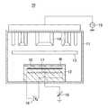
図1は、本実施の形態に係る構成部品の洗浄方法を実行するウエハドライクリーニング装置の構成を概略的に示す断面図である。このウエハドライクリーニング装置は半導体ウエハ(以下、単に「ウエハ」という)Wの表面に付着した異物(以下、「パーティクル」という)を溶剤又は溶液等を用いずに除去する。 FIG. 1 is a cross-sectional view schematically showing a configuration of a wafer dry cleaning apparatus that executes a component cleaning method according to the present embodiment. This wafer dry cleaning apparatus removes foreign matter (hereinafter referred to as “particles”) adhering to the surface of a semiconductor wafer (hereinafter simply referred to as “wafer”) W without using a solvent or a solution.
図1において、ウエハドライクリーニング装置10(基板処理装置)は、処理室11と、該処理室11内の底部に設けられた載置台12と、載置台12と所定の間隔を隔ててその上方に対向配置された捕集板13(構成部品)と、該捕集板13の上方に配置されたプラズマ生成装置14とを備える。載置台12にはウエハWが載置される。 In FIG. 1, a wafer dry cleaning apparatus 10 (substrate processing apparatus) includes a
載置台12は絶縁材によって構成されるとともに、静電電極板15を内蔵し、該静電電極板15は第1の直流電源16に接続されている。静電電極板15に第1の直流電源16から正の直流電圧が印加されると、ウエハWにおける載置台12側の面(以下、「裏面」という。)に電子が引き寄せられるが、載置台12は絶縁材からなるため、電子はそこに留まり、ウエハWの裏面に負電位が発生する。このとき、ウエハWにおける電子の偏在の反作用によってウエハWにおける捕集板13側の面(以下、「表面」という。)には正電位が発生する。ウエハWの裏面に負電位が発生すると、静電電極板15及びウエハWの裏面の間に電位差が生じ、該電位差に起因するクーロン力又はジョンソン・ラーベック力により、ウエハWは載置台12に吸着保持される。また、載置台12には、ウエハWを加熱する電熱ヒータ17が内蔵されており、電熱ヒータ17は、第2の直流電源18に接続されている。 The mounting table 12 is made of an insulating material and incorporates an
捕集板13は、例えば、Y2O3、石英、ポリテトラフルオロエチレン(商品名:テフロン(登録商標))、Si、Al、Al2O3、SiO2等からなる厚さ0.5〜10mmの平板からなり、その表面の面粗度はパーティクルが付着するように或る値以上に設定される。The
プラズマ生成装置14は、誘導結合プラズマ(ICP:Inductive Coupling Plasma)生成装置であり、高周波電源19に接続され、処理室11内に導入された処理ガスから表面波プラズマを生成し、処理室11内にプラズマを充填する。なお、プラズマ生成装置14は表面波プラズマを生成する装置であればよく、例えば、RLSA(Radial Line Slot Antenna) マイクロ波プラズマ生成装置やリモートプラズマ生成装置を用いることができる。 The
ウエハドライクリーニング装置10においてウエハWの表面に付着したパーティクルを除去する場合、まず、ウエハWを載置台12の上面に載置し、処理室11内の圧力を圧力調整装置(図示しない)によって所定値に調整する。 When removing particles adhering to the surface of the wafer W in the wafer
次いで、電熱ヒータ17で、ウエハWを、例えば、ウエハWに形成されたフォトレジスト膜の耐熱温度上限、例えば150℃まで加熱して、ウエハWの表面に付着したパーティクルに熱応力と熱泳動力を作用させる。これにより、パーティクルがウエハWの表面から剥離し、且つ離脱する。すなわち、ウエハWが150℃に加熱されたとき、パーティクルは、熱応力によってウエハWから剥離する。また、このとき、載置台12に対向配置された捕集板13は加熱されていないので、ウエハWの表面と捕集板13の温度差が大きくなり、ウエハWに付着したパーティクルを囲む雰囲気に温度勾配が生じる。この温度勾配に基づいて、ウエハWの表面から剥離したパーティクルには、高温側であるウエハWの表面から、低温側である捕集板13に向かう熱泳動力が作用し、これにより、パーティクルは捕集板13に向かって移動して捕集板13に付着・捕捉される。 Next, the wafer W is heated by the
ここで、熱泳動力とは、以下のように定義される。すなわち、粒子が存在する空間中に大きな温度勾配があるとき、粒子に衝突する気体分子の運動量は、粒子の高温側と低温側とを比較すると高温側の方が大きくなり、これによって、粒子は高温側から低温側へ向かう力を受けるが、このとき粒子が受ける力を熱泳動力という。熱泳動力が大きく作用するのは、圧力が1.3×10Pa(100mTorr)〜1.3kPa(10Torr)の場合であるため、ウエハWの表面からパーティクルを除去する際、処理室11内の圧力を上記圧力範囲に調整するのが好ましい。 Here, the thermophoretic force is defined as follows. That is, when there is a large temperature gradient in the space where the particles exist, the momentum of the gas molecules that collide with the particles is higher on the high temperature side than on the high temperature side and the low temperature side of the particle. A force from the high temperature side toward the low temperature side is received, and the force that the particles receive at this time is called a thermophoretic force. Since the thermophoretic force acts greatly when the pressure is 1.3 × 10 Pa (100 mTorr) to 1.3 kPa (10 Torr), the pressure in the
このウエハドライクリーニング装置10においてウエハWの表面に付着したパーティクルの除去を繰り返すと、捕集板13に付着するパーティクルが増加するために捕集板13に付着したパーティクルを除去する必要がある。 When the removal of particles adhering to the surface of the wafer W is repeated in the wafer
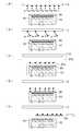
図2は、本実施の形態に係る構成部品の洗浄方法としての捕集板洗浄処理を示す工程図である。本処理は、例えば、洗浄対象のウエハWが処理室11から搬出された後に実行される。 FIG. 2 is a process diagram showing a collecting plate cleaning process as a component cleaning method according to the present embodiment. This process is executed, for example, after the wafer W to be cleaned is unloaded from the
図2において、まず、処理室11内へダミーウエハ20(異物吸着部材)を搬入して載置台12に載置し、第1の直流電源16から静電電極板15へ正の直流電圧を印加してダミーウエハ20を載置台12に静電吸着する(搬入ステップ)。このとき、ダミーウエハ20の表面には正電位が発生する(図2(A))。なお、ダミーウエハ20が再び処理室11の外へ搬出されるまで静電電極板15へ正の直流電圧は印加され続けるため、ダミーウエハ20の表面にも正電位が発生したままである。 In FIG. 2, first, a dummy wafer 20 (foreign matter adsorbing member) is loaded into the
次いで、処理室11内を図示しない排気装置によって高真空状態(例えば、1.3×10⁻³Pa(1.0×10⁻⁵Torr)以下)まで減圧し、処理室11内に、例えばアルゴンガスを主成分とする処理ガスを導入し、さらに、高周波電源19からプラズマ生成装置14へ高周波電圧を印加して表面波プラズマを生成し、処理室11内にプラズマを充填する。ウエハドライクリーニング装置10では、載置台12に静電吸着されたダミーウエハ20よりも捕集板13がプラズマ生成装置14の近傍に位置するため、結果として、ダミーウエハ20よりも捕集板13の近傍で表面波プラズマが生成されることになり、ダミーウエハ20の近傍のプラズマ密度よりも捕集板13の近傍のプラズマ密度が高くなる。その結果、捕集板13はプラズマ中の陽イオン(図中「○+」で示す。)によってスパッタされやすくなり、捕集板13に付着したパーティクル(図中「●」で示す。)は陽イオンのスパッタリングによって捕集板13から剥離する(図2(A))。Next, the inside of the
剥離したパーティクルは処理室11内へ飛散し、プラズマ中の電子(図中「e−」で示す。)と衝突する。このとき、パーティクルは負に帯電し、該パーティクルには負電位が発生する(図2(B))。The peeled particles scatter into the
また、処理室11内にプラズマが存在している間、該プラズマに起因してダミーウエハ20の表面近傍や捕集板13の表面近傍にはシース21a,21bが発生する(図2(C))。シースはイオン密度が高い領域であり、正電位の陽イオンには引力である静電気力を作用させて該陽イオンをダミーウエハ20や捕集板13に向けて加速させるが、負電位の電子やパーティクルには反発力である静電気力を作用させてダミーウエハ20や捕集板13から遠ざける。その結果、負電位のパーティクルは重力やシース21a,21bからの静電気力の釣り合いに応じて処理室11内を漂う(図2(C))。なお、シース21aによってダミーウエハ20へも陽イオンが引き込まれるため、該ダミーウエハ20も陽イオンによってスパッタされるが、上述したように、ダミーウエハ20はプラズマ生成装置14から遠いため、ダミーウエハ20近傍のプラズマ密度は低くなり、シース21aも薄くなる。そのため、ダミーウエハ20へ引き込まれる陽イオンの数は少なく、且つエネルギーも小さい。したがって、後述するようにダミーウエハ20へ吸着したパーティクルが陽イオンのスパッタリングによって再飛散することは殆どあり得ない。 Further, while plasma is present in the
次いで、高周波電源19からの高周波電圧の印加を中止してプラズマ生成装置14による表面波プラズマの生成を中止すると、シース21a,21bが消滅する。特に、シース21aが消滅すると、該シース21aの近傍に存在しているパーティクルにはシース21aからの反発力である静電気力が作用しなくなり、また、該パーティクルは正電位のダミーウエハ20と対峙する。このとき、負電位のパーティクルと正電位のダミーウエハ20の間には引力である静電気力が発生し、パーティクルはダミーウエハ20へ引き寄せられて吸着する(図2(D))。 Next, when the application of the high-frequency voltage from the high-
本処理では、プラズマ生成装置14による表面波プラズマの生成及び表面波プラズマの生成の中止、すなわち、図2(A)〜図2(C)に示される捕集板13からのパーティクルの剥離(生成ステップ)、及び図2(D)に示されるダミーウエハ20へのパーティクルの吸着(消滅ステップ)を繰り返す。これにより、捕集板13からのパーティクルの剥離、及びダミーウエハ20へのパーティクルの吸着を確実に実行する。 In this process, the generation of the surface wave plasma by the
プラズマ生成装置14によって表面波プラズマを生成する時間(第1の所定の時間)は、捕集板13からの少なくとも一部のパーティクルが剥離するために充分な時間であるのが好ましく、また、プラズマ生成装置14による表面波プラズマの生成を中止する時間(第2の所定の時間)は、捕集板13から剥離した一部のパーティクルがダミーウエハ20の正電位に起因する静電気力によって該ダミーウエハ20へ引き寄せられて到達するために充分な時間であるのが好ましい。 The time (first predetermined time) for generating the surface wave plasma by the
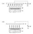
また、本処理では、高周波電圧をパルス波的に印加すると制御が容易であるため、プラズマ生成装置14による表面波プラズマの生成及び表面波プラズマの生成の中止の繰り返しを、図3(A)に示すように、パルス波的に行う。パルス波の周波数が高い、例えば、1KHz以上である場合、プラズマ生成装置14への高周波電圧の印加を中止しても表面波プラズマの生成が停止しない。また、表面波プラズマを生成するときに捕集板13を充分にスパッタし、且つ表面波プラズマを消滅させるときにシースを確実に消滅させてダミーウエハ20へのパーティクルの吸着を円滑に行うために、表面波プラズマの生成及び表面波プラズマの生成の中止をそれぞれ或る程度の時間だけ継続する必要がある。したがって、パルス波の周波数は低い方が好ましく、例えば、10Hz〜100Hzであるのがよい。 Further, in this process, since it is easy to control when a high-frequency voltage is applied in the form of a pulse wave, repetition of generation of surface wave plasma and stop of generation of surface wave plasma by the
なお、プラズマ生成装置14による表面波プラズマの生成及び表面波プラズマの生成の中止の繰り返しを、図3(B)に示すように、サイン波的に行ってもよい。この場合、負電位のパーティクルに作用する静電気力の変化、例えば、反発力から引力への変化、又は引力から反発力への変化を穏やかに行うことができ、急激な静電気力の変化に起因してパーティクルが思わぬ場所へ飛散する等の不具合を防止することができる。 It should be noted that the generation of surface wave plasma and the stop of the generation of surface wave plasma by the
次いで、第1の直流電源16から静電電極板15への正の直流電圧の印加を中止してダミーウエハ20の静電吸着を中止し、ダミーウエハ20を処理室11の外へ搬出し(搬出ステップ)(図2(E))、本処理を終了する。 Next, the application of the positive DC voltage from the first
図2の捕集板洗浄処理によれば、処理室11内へダミーウエハ20が搬入され、ダミーウエハ20の表面に正電位が発生した後、ダミーウエハ20よりも捕集板13の近傍での表面波プラズマの生成及び表面波プラズマの生成の中止が交互に繰り返され、その後、処理室11内からダミーウエハ20が搬出される。このとき、処理室11内において、プラズマのスパッタリングによる捕集板13からのパーティクルの剥離、及び静電気力によるダミーウエハ20へのパーティクルの吸着が交互に繰り返されるので、捕集板13を処理室11から取り出すことなく、且つ該捕集板13に付着したパーティクルをウエハドライクリーニング装置10の他の構成部品へ吸着させることなく、パーティクルをダミーウエハ20へ転移させることができる。その結果、パーティクルの他の構成部品への付着を防止しつつ容易に捕集板13を洗浄することができる。 2, after the
上述した図2の捕集板洗浄処理では、処理室11内へ搬入されたダミーウエハ20は載置台12を覆うので、捕集板13から剥離したパーティクルが載置台12に付着するのを防止することができる。また、パーティクルをダミーウエハ20へ吸着させるので、ダミーウエハ20を搬出するだけで処理室11内からパーティクルを除去することができる。通常、ウエハドライクリーニング装置10はダミーウエハ20を含むウエハを搬出入する機構(図示しない)を備えているため、パーティクルの除去のためだけに新たな機構を追加する必要性を無くすことができる。 In the above-described collection plate cleaning process of FIG. 2, the
通常、平行平板型のプラズマ装置を用いると、プラズマを生成する際に、該プラズマ装置の電極へ印加する高周波電圧をマッチングする必要があり、該マッチングには或る程度の時間を要するため、プラズマの生成及び消滅を繰り返す場合、プラズマが生成される時間が短時間であると、プラズマを充分に生成させられない虞がある。しかしながら、上述した図2の捕集板洗浄処理では、表面波プラズマを生成する誘導結合プラズマ装置であるプラズマ生成装置14を用いて処理室11内にプラズマを充填するので、高周波電圧のマッチングを必要としない。したがって、プラズマの生成時間が短時間であっても安定してプラズマを処理室11内に存在させることができ、プラズマのスパッタリングによる捕集板13からのパーティクルの剥離を確実に行うことができる。 Usually, when a parallel plate type plasma apparatus is used, it is necessary to match the high frequency voltage applied to the electrodes of the plasma apparatus when generating plasma, and this matching requires a certain amount of time. In the case where the generation and extinction are repeated, if the plasma is generated for a short time, the plasma may not be generated sufficiently. However, in the collection plate cleaning process of FIG. 2 described above, the plasma is filled in the
上述した図2の捕集板洗浄処理では、ダミーウエハ20を載置台12に載置して静電吸着したが、ダミーウエハ20の代わりに帯電して正電位が発生している平板状のカバー21を異物吸着部材として処理室11内に挿入し、載置台12に載置することなく捕集板13及び載置台12の間において該載置台12を覆うように配置してもよい(図4(A))。この場合、捕集板13から剥離した負電位のパーティクルはカバー21に吸着するため、該カバー21を処理室11の外へ搬出することによって処理室11内からパーティクルを除去することができる。また、カバー21も載置台12を覆うので、捕集板13から剥離したパーティクルが載置台12に付着するのを防止することができる。 In the collection plate cleaning process of FIG. 2 described above, the
また、処理室11内へ挿入される異物吸着部材は上述したカバー21に限られない、例えば、図4(B)及び図4(C)に示す、帯電して正電位が発生しているリング状部材22を挿入してもよく、若しくは、図4(D)に示す、帯電して正電位が発生している棒状部材23を挿入してもよい。この場合も、捕集板13から剥離した負電位のパーティクルはリング状部材22又は棒状部材23に吸着する。なお、リング状部材22や棒状部材23にはパーティクルを雰囲気と共に吸引する複数の吸引口22a,22bを有するのが好ましい。これにより、リング状部材22や棒状部材23の正電位によって引き寄せられた負電位のパーティクルを吸引して処理室11の外へ排出することができる。 Further, the foreign matter adsorbing member inserted into the
上述した図2の捕集板洗浄処理において、プラズマのスパッタリングによる捕集板13からのパーティクルの剥離の際、捕集板13へ他の高周波電源24からバイアス電圧を印加してもよい(図5(A))。この場合、バイアス電圧によってプラズマを捕集板13へ確実に引き込むことができ、もって、パーティクルの剥離を促進することができる。 In the collection plate cleaning process of FIG. 2 described above, a bias voltage may be applied to the
また、プラズマのスパッタリングによる捕集板13からのパーティクルの剥離の際、捕集板13へ熱、衝撃及び振動の少なくとも1つを付与してもよい。これにより、熱応力や衝撃力をパーティクルに作用させてパーティクルの剥離を促進することができる。 Further, at the time of peeling of particles from the
なお、上述した図2の捕集板洗浄処理では、処理室11内にプラズマが充填される際、ダミーウエハ20へのプラズマのスパッタリングを防止するために、載置台12へはバイアス電圧を印加しない方が好ましい。 In the above-described collection plate cleaning process of FIG. 2, when plasma is filled in the
上述した図2の捕集板洗浄処理において、静電気力によるダミーウエハ20へのパーティクルの吸着の際、第3の直流電源25から捕集板13へ負の直流電圧を印加し、該捕集板13を負電位にしてもよい(図5(B))。この場合、捕集板13には負電位が発生し、負電位のパーティクルには捕集板13から遠ざけるように作用する静電気力が付与されるため、ダミーウエハ20へのパーティクルの吸着を促進することができるとともに、負電位のパーティクルの捕集板13への再付着を防止できる。 In the collection plate cleaning process of FIG. 2 described above, a negative DC voltage is applied from the third
上述した図2の捕集板洗浄処理では、パーティクルのダミーウエハ20への吸着に静電気力のみを用いたが、静電気力に加えて熱泳動力も用いることもできる。この場合、図6に示すように、捕集板13に電熱ヒータ26を内蔵するとともに載置台12にペルティエ素子27を内蔵し、表面波プラズマの生成を中止する際、電熱ヒータ26によって捕集板13を加熱し、且つペルティエ素子27によってダミーウエハ20を冷却して捕集板13及びダミーウエハ20の間の雰囲気に温度勾配を生じさせる。この温度勾配に基づいてパーティクルには高温側である捕集板13から、低温側であるダミーウエハ20に向かう熱泳動力が作用する。これにより、ダミーウエハ20へのパーティクルの吸着をさらに促進することができる。 In the collection plate cleaning process of FIG. 2 described above, only the electrostatic force is used for adsorbing particles to the
また、ダミーウエハ20がその表面に付着したパーティクルを絡め取るパーティクル捕捉部28を有してもよい(図6)。パーティクル捕捉部28としては、例えば、プラズマ耐性を有するメッシュ状の構造物や不織布、若しくは粘着シートを用いることができる。
パーティクル捕捉部28を用いることによってダミーウエハ20が吸着したパーティクルが再飛散するのを防止することができ、もって、処理室11内が再飛散したパーティクルによって再度汚染させるのを防止することができる。なお、このときも熱泳動力を大きく作用させるために、処理室11内の圧力を1.3×10Pa(100mTorr)〜1.3kPa(10Torr)に調整するのが好ましい。Further, the
By using the
なお、上述した図2の捕集板洗浄処理では、捕集板13からのパーティクルの剥離及びダミーウエハ20へのパーティクルの吸着の繰り返しの間、静電電極板15への正の直流電圧の印加を継続して行っているが、捕集板13からのパーティクルの剥離の際、ダミーウエハ20の表面に正電位が発生しても、シース21aが負電位のパーティクルを反発力としての静電気力によってダミーウエハ20から遠ざけるため、ダミーウエハ20の表面の正電位に起因する静電気力がパーティクルに殆ど作用しない。したがって、捕集板13からのパーティクルの剥離の際には静電電極板15への正の直流電圧の印加を行わず、ダミーウエハ20へのパーティクルの吸着の際のみ静電電極板15への正の直流電圧の印加を行ってもよい。 In the collection plate cleaning process of FIG. 2 described above, a positive DC voltage is applied to the
次に、本発明の第2の実施の形態に係る構成部品の洗浄方法について説明する。 Next, a component cleaning method according to the second embodiment of the present invention will be described.
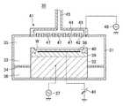
図7は、本実施の形態に係る構成部品の洗浄方法を実行するプラズマエッチング装置の構成を概略的に示す断面図である。このプラズマエッチング装置はウエハWに、例えば、ドライエッチング処理を施す。 FIG. 7 is a cross-sectional view schematically showing a configuration of a plasma etching apparatus that executes the component cleaning method according to the present embodiment. This plasma etching apparatus performs, for example, a dry etching process on the wafer W.
図7において、プラズマエッチング装置30(基板処理装置)は、例えば、直径が300mmのウエハWを収容するチャンバ31(処理室)を有し、該チャンバ31内の下方にはウエハWを載置する円柱状のサセプタ32(載置台)が配置されている。また、プラズマエッチング装置30では、チャンバ31の内側壁とサセプタ32の側面とによって側方排気路33が形成される。この側方排気路33の途中には排気プレート34が配置される。 In FIG. 7, the plasma etching apparatus 30 (substrate processing apparatus) has, for example, a chamber 31 (processing chamber) that accommodates a wafer W having a diameter of 300 mm, and the wafer W is placed below the
排気プレート34は多数の孔を有する板状部材であり、チャンバ31内部を上部と下部に仕切る仕切り板として機能する。排気プレート34によって仕切られたチャンバ31内部の上部(以下、「反応室」という。)35にはプラズマが発生する。また、チャンバ31内部の下部(以下、「排気室(マニホールド)」という。)36にはチャンバ31内のガスを排出する排気装置(図示しない)が接続される。排気プレート34は反応室35に発生するプラズマを捕捉又は反射してマニホールド36への漏洩を防止する。 The
排気装置はチャンバ31内を高真空状態(例えば、1.3×10⁻³Pa(1.0×10⁻⁵Torr)以下)まで減圧する。なお、チャンバ31内の圧力は圧力調整装置(図示しない)によって制御される。The exhaust device depressurizes the inside of the
チャンバ31内のサセプタ32には第1の高周波電源37が接続されており、第1の高周波電源37はバイアス電圧をサセプタ32に印加する。これにより、サセプタ32は下部電極として機能する。 A first high
サセプタ32の上部には、静電電極板38を内部に有し且つ絶縁材によって構成される静電チャック39が配置され、静電電極板38に直流電源40が接続されている。静電電極板38に正の直流電圧が印加されると、ウエハドライクリーニング装置10のサセプタ32に載置されたウエハWと同様に、ウエハWにおけるサセプタ32側の面(以下、「裏面」という。)に負電位が発生し、且つウエハWにおける裏面とは反対側の面(以下、「表面」という。)には正電位が発生し、該ウエハWはクーロン力又はジョンソン・ラーベック力により、静電チャック39に吸着保持される。 An
静電チャック39には、吸着保持されたウエハWを囲うように、リング状部材であるフォーカスリング40が載置される。フォーカスリング40は、プラズマの分布域をウエハW上だけでなく該フォーカスリング40上まで拡大してウエハWの周縁部上におけるプラズマの密度を該ウエハWの中央部上におけるプラズマの密度と同程度に維持する。 A
チャンバ31の天井部には、サセプタ32と対向するようにシャワーヘッド41が配置されている。シャワーヘッド41は、上部電極42(構成部品)と該上部電極42を着脱可能に釣支するクーリングプレート43とを有する。上部電極42は多数のガス穴47を有する導電性の円板状部材によって構成されている。クーリングプレート43の内部にはバッファ室44が設けられ、このバッファ室44には処理ガス導入管45が接続されている。上部電極42には第2の高周波電源46が接続されており、該第2の高周波電源46は比較的高い周波数のプラズマ生成用の高周波電圧をサセプタ32に印加する。 A
プラズマエッチング装置30では、処理ガス導入管45からバッファ室44へ供給された処理ガスがガス穴47を介して反応室35内へ導入され、該導入された処理ガスは、第2の高周波電源46から上部電極42を介して反応室35内へ印加されたプラズマ生成用の高周波電圧によって励起されてプラズマとなる。該プラズマは、第1の高周波電源37がサセプタ32に印加するバイアス電圧によって静電チャック39に静電吸着されたウエハWへ引きこまれ、該ウエハWにドライエッチング処理を施す。 In the
上述したプラズマエッチング装置30の各構成部品の動作は、プラズマエッチング装置30が備える制御部(図示しない)のCPUが所定のプログラムに応じて制御する。 The operation of each component of the
このプラズマエッチング装置30においてウエハWへのドライエッチング処理を行うと処理ガスに起因する反応生成物やパーティクルが発生することがあり、該ドライエッチング処理を繰り返すと、各構成部品、例えば、上部電極42に付着する反応生成物やパーティクルが付着することがある。付着したパーティクルがウエハWへ落下すると半導体デバイスの欠陥を引き起こすことがあるため、上部電極42に付着した反応生成物やパーティクルを定期的に除去する必要がある。 When a dry etching process is performed on the wafer W in the
図8は、本実施の形態に係る構成部品の洗浄方法としての上部電極洗浄処理を示す工程図である。本処理は、例えば、ドライエッチング処理が所定回数繰り返された後に実行される。 FIG. 8 is a process diagram showing an upper electrode cleaning process as a component cleaning method according to the present embodiment. This process is executed, for example, after the dry etching process is repeated a predetermined number of times.
図8において、まず、反応室35内へダミーウエハ20を搬入して静電チャック39に載置し、直流電源40から静電電極板38へ正の直流電圧を印加してダミーウエハ20を静電チャック39に静電吸着する(搬入ステップ)。このとき、ダミーウエハ20の表面には正電位が発生する(図8(A))。なお、ダミーウエハ20が再び反応室35の外へ搬出されるまで静電電極板38へ正の直流電圧は印加され続けるため、ダミーウエハ20の表面にも正電位が発生したままである。 In FIG. 8, first, the
次いで、反応室35内を排気装置によって高真空状態(例えば、1.3×10⁻³Pa(1.0×10⁻⁵Torr)以下)まで減圧し、反応室35内に、例えば酸素ガスやアルゴンガスを主成分とする処理ガスを導入し、さらに、第2の高周波電源46から上部電極42を介して反応室35内へプラズマ生成用の高周波電圧を印加して処理ガスから、陽イオンやラジカルを含むプラズマを生成し、反応室35内にプラズマを充填する。プラズマエッチング装置30では、上部電極42そのものにプラズマ生成用の高周波電圧を印加するため、結果として、ダミーウエハ20よりも上部電極42の近傍でプラズマが生成されることになり、ダミーウエハ20の近傍のプラズマ密度よりも上部電極42の近傍のプラズマ密度が高くなる。その結果、上部電極42はプラズマ中の陽イオン(図中「○+」で示す。)によってスパッタされやすくなり、上部電極42に付着したパーティクル(図中「●」で示す。)は陽イオンのスパッタリングによって上部電極42から剥離する(図8(A))。なお、このとき、プラズマ中のラジカル(図示しない)も上部電極42へ容易に到達し、上部電極42に付着した反応生成物(図示しない)を分解して除去する。Next, the inside of the
ここで、剥離したパーティクルは反応室35内へ飛散し、プラズマ中の電子(図中「e−」で示す。)と衝突する。このとき、パーティクルは負に帯電し、該パーティクルには負電位が発生する(図8(B))。Here, the peeled particles are scattered into the
また、反応室35内にプラズマが存在している間、該プラズマに起因してダミーウエハ20の表面近傍や上部電極42の表面近傍にはシース48a,48bが発生し(図8(C))、負電位のパーティクルは重力やシース48a,48bからの静電気力の釣り合いに応じて反応室35内を漂う(図8(C))。なお、シース21aと同様の理由でシース48aも薄くなるため、ダミーウエハ20へ吸着したパーティクルが陽イオンのスパッタリングによって再飛散することは殆どあり得ない。 Further, while the plasma is present in the
次いで、第2の高周波電源46からの高周波電圧の印加を中止してプラズマの生成を中止すると、シース48a,48bが消滅し負電位のパーティクルは正電位のダミーウエハ20と対峙し、パーティクルは静電気力によってダミーウエハ20へ引き寄せられて吸着する(図8(D))。 Next, when the application of the high frequency voltage from the second high
本処理でも、上述した図2の捕集板洗浄処理と同様に、反応室35におけるプラズマの生成及びプラズマの消滅、すなわち、図8(A)〜図8(C)に示される上部電極42からのパーティクルの剥離(生成ステップ)、及び図8(D)に示されるダミーウエハ20へのパーティクルの吸着(消滅ステップ)を繰り返す。これにより、上部電極42からのパーティクルの剥離、及びダミーウエハ20へのパーティクルの吸着を確実に実行する。また、本処理でも、上述した図2の捕集板洗浄処理と同様に、プラズマの生成及びプラズマの消滅の繰り返しをパルス波的に行い、パルス波の周波数は10Hz〜100Hzに設定される。なお、本処理でもプラズマの生成及びプラズマの消滅の繰り返しをサイン波的に行ってもよい。 Also in this process, as in the collection plate cleaning process of FIG. 2 described above, plasma is generated and extinguished in the
次いで、直流電源40から静電電極板38への正の直流電圧の印加を中止してダミーウエハ20の静電吸着を中止し、ダミーウエハ20をチャンバ31の外へ搬出し(搬出ステップ)(図8(E))、本処理を終了する。 Next, the application of the positive DC voltage from the
図8の上部電極洗浄処理によれば、反応室35内へダミーウエハ20が搬入され、ダミーウエハ20の表面に正電位が発生した後、ダミーウエハ20よりも上部電極42の近傍でのプラズマの生成及びプラズマの消滅が交互に繰り返され、その後、反応室35内からダミーウエハ20が搬出されるので、上部電極42をチャンバ31から取り出すことなく、且つ該上部電極42に付着したパーティクルをプラズマエッチング装置30の他の構成部品へ吸着させることなく、パーティクルをダミーウエハ20へ転移させることができる。その結果、パーティクルの他の構成部品への付着を防止しつつ容易に上部電極42を洗浄することができる。 According to the upper electrode cleaning process of FIG. 8, after the
また、反応室35内へ搬入されたダミーウエハ20は静電チャック39を覆うので、上部電極42から剥離したパーティクルが静電チャック39に付着するのを防止することができる。 Further, since the
なお、上述した各実施の形態では、ウエハドライクリーニング装置10やプラズマエッチング装置30が処理を施す基板が半導体デバイス用のウエハであったが、処理が施される基板はこれに限られず、例えば、LCD(Liquid Crystal Display)やFPD(Flat Panel Display)等のガラス基板であってもよい。 In each of the above-described embodiments, the substrate to be processed by the wafer
また、本発明の目的は、上述した各実施の形態の機能を実現するソフトウェアのプログラムコードを記録した記憶媒体を、コンピュータ(例えば、制御部)に供給し、コンピュータのCPUが記憶媒体に格納されたプログラムコードを読み出して実行することによっても達成される。 Another object of the present invention is to supply a computer (for example, a control unit) with a storage medium storing software program codes for realizing the functions of the above-described embodiments, and the CPU of the computer is stored in the storage medium. It is also achieved by reading and executing the program code.
この場合、記憶媒体から読み出されたプログラムコード自体が上述した各実施の形態の機能を実現することになり、プログラムコード及びそのプログラムコードを記憶した記憶媒体は本発明を構成することになる。 In this case, the program code itself read from the storage medium realizes the functions of the above-described embodiments, and the program code and the storage medium storing the program code constitute the present invention.
また、プログラムコードを供給するための記憶媒体としては、例えば、RAM、NV−RAM、フロッピー(登録商標)ディスク、ハードディスク、光磁気ディスク、CD−ROM、CD−R、CD−RW、DVD(DVD−ROM、DVD−RAM、DVD−RW、DVD+RW)等の光ディスク、磁気テープ、不揮発性のメモリカード、他のROM等の上記プログラムコードを記憶できるものであればよい。或いは、上記プログラムコードは、インターネット、商用ネットワーク、若しくはローカルエリアネットワーク等に接続される不図示の他のコンピュータやデータベース等からダウンロードすることによりコンピュータに供給されてもよい。 Examples of the storage medium for supplying the program code include RAM, NV-RAM, floppy (registered trademark) disk, hard disk, magneto-optical disk, CD-ROM, CD-R, CD-RW, DVD (DVD). -ROM, DVD-RAM, DVD-RW, DVD + RW) and other optical disks, magnetic tapes, non-volatile memory cards, other ROMs, etc., as long as they can store the program code. Alternatively, the program code may be supplied to the computer by downloading from another computer or database (not shown) connected to the Internet, a commercial network, a local area network, or the like.
また、コンピュータが読み出したプログラムコードを実行することにより、上記各実施の形態の機能が実現されるだけでなく、そのプログラムコードの指示に基づき、CPU上で稼動しているOS(オペレーティングシステム)等が実際の処理の一部又は全部を行い、その処理によって上述した各実施の形態の機能が実現される場合も含まれる。 Further, by executing the program code read by the computer, not only the functions of the above-described embodiments are realized, but also an OS (operating system) running on the CPU based on the instruction of the program code. Includes a case where part or all of the actual processing is performed and the functions of the above-described embodiments are realized by the processing.
更に、記憶媒体から読み出されたプログラムコードが、コンピュータに挿入された機能拡張ボードやコンピュータに接続された機能拡張ユニットに備わるメモリに書き込まれた後、そのプログラムコードの指示に基づき、その機能拡張ボードや機能拡張ユニットに備わるCPU等が実際の処理の一部又は全部を行い、その処理によって上述した各実施の形態の機能が実現される場合も含まれる。 Further, after the program code read from the storage medium is written in a memory provided in a function expansion board inserted into the computer or a function expansion unit connected to the computer, the function expansion is performed based on the instruction of the program code. This includes a case where the CPU or the like provided in the board or the function expansion unit performs part or all of the actual processing, and the functions of the above-described embodiments are realized by the processing.
上記プログラムコードの形態は、オブジェクトコード、インタプリタにより実行されるプログラムコード、OSに供給されるスクリプトデータ等の形態から成ってもよい。 The form of the program code may include an object code, a program code executed by an interpreter, script data supplied to the OS, and the like.
W ウエハ
10 ウエハドライクリーニング装置
11 処理室
12 載置台
13 捕集板
14 プラズマ生成装置
20 ダミーウエハ
30 プラズマエッチング装置
31 チャンバ
32 サセプタ
39 静電チャック
42 上部電極W wafer
DESCRIPTION OF
Claims (12)
Translated fromJapanese前記処理室内へ前記異物吸着部材を搬入する搬入ステップと、
前記異物吸着部材よりも前記構成部品の近傍でプラズマを生じさせ、前記プラズマ中の陽イオンによるスパッタリングによって前記構成部品から異物を剥離させる生成ステップと、
前記プラズマを消滅させる消滅ステップと、
前記処理室内から前記異物吸着部材を搬出する搬出ステップとを有し、
前記生成ステップ及び前記消滅ステップを交互に繰り返し、前記異物吸着部材を少なくとも前記消滅ステップにおいて正電位にすることにより、前記構成部品から剥離して前記プラズマ中の電子と衝突して負電位となる前記異物を前記異物吸着部材に吸着させること特徴とする構成部品の洗浄方法。A cleaning method for component parts in a substrate processing apparatus, comprising: a processing chamber; and a component having at least a part facing the processing chamber to which foreign matter is adhered, wherein the foreign matter adsorbing member can be carried in and out of the processing chamber. And
A carrying-in step of carrying in the foreign matter adsorbing member into the processing chamber;
Than said foreign matter capture member causing a plasma in the vicinity of thecomponent, a generationstep by sputtering by cations in the plasma Ruis peeled foreign matter from the component,
An extinction step for extinguishing the plasma;
Carrying out the foreign matter adsorbing member from the processing chamber;
Alternately repeating said generating step and the extinctionstep,by a positive potential at the annihilation step evenpre Symbol foreign matter capture membersmallwithout electrons collide with a negative potential of the plasma is peeled from the component The cleaning method for component parts,wherein the foreign matter is adsorbed to the foreign matter adsorbing member .
前記第1の所定の時間は、プラズマのスパッタリングによって前記構成部品から少なくとも一部の前記異物が剥離するために充分な時間であり、前記第2の所定の時間は少なくとも一部の前記剥離した異物が前記異物吸着部材の正電位によって引き寄せられて該異物吸着部材に到達するために充分な時間であることを特徴とする請求項1記載の構成部品の洗浄方法。In the generating step, the plasma is generated for a first predetermined time, and in the extinguishing step, the plasma is extinguished for a second predetermined time,
The first predetermined time is a time sufficient for peeling at least a part of the foreign matter from the component by plasma sputtering, and the second predetermined time is at least a part of the peeled foreign matter. 2. The method of cleaning a component according to claim 1, wherein the time is sufficient to reach the foreign matter adsorbing member by being attracted by the positive potential of the foreign matter adsorbing member.
前記基板乾燥洗浄装置は前記処理室内に配置され且つ前記ダミーウエハを載置する載置台を備え、
前記処理室内へ搬入された前記ダミーウエハは前記載置台を覆うことを特徴とする請求項1乃至9のいずれか1項に記載の構成部品の洗浄方法。The substrate processing apparatus is a substrate drying and cleaning apparatus, the component is a foreign material collecting plate, and the foreign material adsorption member is a dummy wafer,
The substrate drying and cleaning apparatus includes a mounting table disposed in the processing chamber and mounting the dummy wafer.
The method for cleaning a component according to claim 1, wherein the dummy wafer carried into the processing chamber covers the mounting table.
前記プラズマエッチング装置は前記処理室内に配置され且つ前記ダミーウエハを載置する載置台をさらに備え、
前記処理室内へ搬入された前記ダミーウエハは前記載置台を覆うことを特徴とする請求項1乃至9のいずれか1項に記載の構成部品の洗浄方法。The substrate processing apparatus is a plasma etching apparatus, the component is an upper electrode, and the foreign matter adsorbing member is a dummy wafer;
The plasma etching apparatus further includes a mounting table disposed in the processing chamber and on which the dummy wafer is mounted.
The method for cleaning a component according to claim 1, wherein the dummy wafer carried into the processing chamber covers the mounting table.
前記処理室内へ前記異物吸着部材を搬入する搬入ステップと、
前記異物吸着部材よりも前記構成部品の近傍でプラズマを生じさせ、前記プラズマ中の陽イオンによるスパッタリングによって前記構成部品から異物を剥離させる生成ステップと、
前記プラズマを消滅させる消滅ステップと、
前記処理室内から前記異物吸着部材を搬出する搬出ステップとを有し、
前記生成ステップ及び前記消滅ステップを交互に繰り返し、前記異物吸着部材を、少なくとも前記消滅ステップにおいて正電位にすることにより、前記構成部品から剥離して前記プラズマ中の電子と衝突して負電位となる前記異物を前記異物吸着部材に吸着させることを特徴とする記憶媒体。A method of cleaning a component in a substrate processing apparatus, comprising: a processing chamber; and a component having at least a portion facing the processing chamber to which foreign matter is attached, wherein a foreign matter adsorbing member can be carried in and out of the processing chamber. A computer-readable storage medium storing a program to be executed by the computer, wherein the cleaning method includes:
A carrying-in step of carrying in the foreign matter adsorbing member into the processing chamber;
Than said foreign matter capture member causing a plasma in the vicinity of thecomponent, a generationstep by sputtering by cations in the plasma Ruis peeled foreign matter from the component,
An extinction step for extinguishing the plasma;
Carrying out the foreign matter adsorbing member from the processing chamber;
Alternately repeating said generating step and the extinctionstep, thepre-Symbol foreign matter capture member,by a positive potential at least the annihilationstep, a negative potential peeled collide with electrons in the plasma from the component The storage medium is characterizedby adsorbing the foreign matter to the foreign matter adsorbing member .
Priority Applications (4)
| Application Number | Priority Date | Filing Date | Title |
|---|---|---|---|
| JP2008322670AJP5295748B2 (en) | 2008-12-18 | 2008-12-18 | Component cleaning method and storage medium |
| US12/639,586US8236109B2 (en) | 2008-12-18 | 2009-12-16 | Component cleaning method and storage medium |
| KR1020090126241AKR101204175B1 (en) | 2008-12-18 | 2009-12-17 | Component cleaning method and storage medium |
| CN2009102606369ACN101752224B (en) | 2008-12-18 | 2009-12-18 | Component cleaning method |
Applications Claiming Priority (1)
| Application Number | Priority Date | Filing Date | Title |
|---|---|---|---|
| JP2008322670AJP5295748B2 (en) | 2008-12-18 | 2008-12-18 | Component cleaning method and storage medium |
Publications (2)
| Publication Number | Publication Date |
|---|---|
| JP2010147238A JP2010147238A (en) | 2010-07-01 |
| JP5295748B2true JP5295748B2 (en) | 2013-09-18 |
Family
ID=42264270
Family Applications (1)
| Application Number | Title | Priority Date | Filing Date |
|---|---|---|---|
| JP2008322670AExpired - Fee RelatedJP5295748B2 (en) | 2008-12-18 | 2008-12-18 | Component cleaning method and storage medium |
Country Status (4)
| Country | Link |
|---|---|
| US (1) | US8236109B2 (en) |
| JP (1) | JP5295748B2 (en) |
| KR (1) | KR101204175B1 (en) |
| CN (1) | CN101752224B (en) |
Families Citing this family (38)
| Publication number | Priority date | Publication date | Assignee | Title |
|---|---|---|---|---|
| EP2688690B1 (en)* | 2011-03-23 | 2019-10-23 | SRI International | Active electroadhesive cleaning |
| US9358590B2 (en) | 2011-03-23 | 2016-06-07 | Sri International | Electroadhesive surface cleaner |
| CN103035466B (en)* | 2011-10-08 | 2016-06-08 | 北京北方微电子基地设备工艺研究中心有限责任公司 | A kind of pre-cleaning method and plasma apparatus |
| JP6313591B2 (en) | 2013-12-20 | 2018-04-18 | キヤノン株式会社 | Imprint apparatus, foreign matter removing method, and article manufacturing method |
| JP6397680B2 (en)* | 2014-07-24 | 2018-09-26 | 株式会社日立ハイテクノロジーズ | Plasma processing apparatus and method of operating plasma processing apparatus |
| US10023956B2 (en)* | 2015-04-09 | 2018-07-17 | Lam Research Corporation | Eliminating first wafer metal contamination effect in high density plasma chemical vapor deposition systems |
| US10786837B2 (en)* | 2015-11-30 | 2020-09-29 | Tokyo Electron Limited | Method for cleaning chamber of substrate processing apparatus |
| US10510575B2 (en) | 2017-09-20 | 2019-12-17 | Applied Materials, Inc. | Substrate support with multiple embedded electrodes |
| CN107863304B (en)* | 2017-11-08 | 2020-08-04 | 上海华力微电子有限公司 | Method for detecting particle pollutants on surface of electrostatic chuck |
| US10760158B2 (en) | 2017-12-15 | 2020-09-01 | Lam Research Corporation | Ex situ coating of chamber components for semiconductor processing |
| US10555412B2 (en) | 2018-05-10 | 2020-02-04 | Applied Materials, Inc. | Method of controlling ion energy distribution using a pulse generator with a current-return output stage |
| KR20250110938A (en) | 2018-10-19 | 2025-07-21 | 램 리써치 코포레이션 | In situ protective coating of chamber components for semiconductor processing |
| US11476145B2 (en) | 2018-11-20 | 2022-10-18 | Applied Materials, Inc. | Automatic ESC bias compensation when using pulsed DC bias |
| KR102827481B1 (en) | 2019-01-22 | 2025-06-30 | 어플라이드 머티어리얼스, 인코포레이티드 | Feedback loop to control pulse voltage waveform |
| US11508554B2 (en) | 2019-01-24 | 2022-11-22 | Applied Materials, Inc. | High voltage filter assembly |
| JP2021118323A (en)* | 2020-01-29 | 2021-08-10 | Hoya株式会社 | Electrostatic Chuck Cleaner and Cleaning Method for Electrostatic Chuck |
| US11607716B1 (en) | 2020-06-23 | 2023-03-21 | Kla Corporation | Systems and methods for chuck cleaning |
| US11848176B2 (en) | 2020-07-31 | 2023-12-19 | Applied Materials, Inc. | Plasma processing using pulsed-voltage and radio-frequency power |
| US11901157B2 (en) | 2020-11-16 | 2024-02-13 | Applied Materials, Inc. | Apparatus and methods for controlling ion energy distribution |
| US11798790B2 (en) | 2020-11-16 | 2023-10-24 | Applied Materials, Inc. | Apparatus and methods for controlling ion energy distribution |
| US11495470B1 (en) | 2021-04-16 | 2022-11-08 | Applied Materials, Inc. | Method of enhancing etching selectivity using a pulsed plasma |
| US11791138B2 (en) | 2021-05-12 | 2023-10-17 | Applied Materials, Inc. | Automatic electrostatic chuck bias compensation during plasma processing |
| US11948780B2 (en) | 2021-05-12 | 2024-04-02 | Applied Materials, Inc. | Automatic electrostatic chuck bias compensation during plasma processing |
| US11967483B2 (en) | 2021-06-02 | 2024-04-23 | Applied Materials, Inc. | Plasma excitation with ion energy control |
| US12394596B2 (en) | 2021-06-09 | 2025-08-19 | Applied Materials, Inc. | Plasma uniformity control in pulsed DC plasma chamber |
| US20220399185A1 (en) | 2021-06-09 | 2022-12-15 | Applied Materials, Inc. | Plasma chamber and chamber component cleaning methods |
| US11810760B2 (en) | 2021-06-16 | 2023-11-07 | Applied Materials, Inc. | Apparatus and method of ion current compensation |
| US11569066B2 (en) | 2021-06-23 | 2023-01-31 | Applied Materials, Inc. | Pulsed voltage source for plasma processing applications |
| US11776788B2 (en) | 2021-06-28 | 2023-10-03 | Applied Materials, Inc. | Pulsed voltage boost for substrate processing |
| CN115705988B (en)* | 2021-08-09 | 2025-10-03 | 长鑫存储技术有限公司 | Jig wafer, cleaning jig, and cleaning method |
| US11476090B1 (en) | 2021-08-24 | 2022-10-18 | Applied Materials, Inc. | Voltage pulse time-domain multiplexing |
| US12106938B2 (en) | 2021-09-14 | 2024-10-01 | Applied Materials, Inc. | Distortion current mitigation in a radio frequency plasma processing chamber |
| US11694876B2 (en) | 2021-12-08 | 2023-07-04 | Applied Materials, Inc. | Apparatus and method for delivering a plurality of waveform signals during plasma processing |
| US11972924B2 (en) | 2022-06-08 | 2024-04-30 | Applied Materials, Inc. | Pulsed voltage source for plasma processing applications |
| US12315732B2 (en) | 2022-06-10 | 2025-05-27 | Applied Materials, Inc. | Method and apparatus for etching a semiconductor substrate in a plasma etch chamber |
| US12272524B2 (en) | 2022-09-19 | 2025-04-08 | Applied Materials, Inc. | Wideband variable impedance load for high volume manufacturing qualification and on-site diagnostics |
| US12111341B2 (en) | 2022-10-05 | 2024-10-08 | Applied Materials, Inc. | In-situ electric field detection method and apparatus |
| CN118866645B (en)* | 2024-09-23 | 2025-02-14 | 无锡尚积半导体科技股份有限公司 | Hierarchical electrostatic adsorption etching device |
Family Cites Families (13)
| Publication number | Priority date | Publication date | Assignee | Title |
|---|---|---|---|---|
| JPH0786259A (en)* | 1993-07-19 | 1995-03-31 | Hitachi Ltd | Foreign object removing method and apparatus |
| JP3191139B2 (en)* | 1994-12-14 | 2001-07-23 | 株式会社日立製作所 | Sample holding device |
| JP3405439B2 (en)* | 1996-11-05 | 2003-05-12 | 株式会社荏原製作所 | How to clean solid surfaces |
| US6093332A (en)* | 1998-02-04 | 2000-07-25 | Lam Research Corporation | Methods for reducing mask erosion during plasma etching |
| KR20030049086A (en) | 2001-12-14 | 2003-06-25 | (주)에이피엘 | System and method for dry cleaning of substrate |
| US7122125B2 (en)* | 2002-11-04 | 2006-10-17 | Applied Materials, Inc. | Controlled polymerization on plasma reactor wall |
| KR20040107983A (en)* | 2003-06-16 | 2004-12-23 | 삼성전자주식회사 | Aperture for manufacturing a semiconductor device |
| US20050241762A1 (en)* | 2004-04-30 | 2005-11-03 | Applied Materials, Inc. | Alternating asymmetrical plasma generation in a process chamber |
| JP4758159B2 (en)* | 2005-07-19 | 2011-08-24 | 株式会社日立ハイテクノロジーズ | Plasma etching apparatus and fine particle removal method |
| JP4804824B2 (en)* | 2005-07-27 | 2011-11-02 | 株式会社日立ハイテクノロジーズ | Plasma processing equipment |
| JP2008027798A (en)* | 2006-07-24 | 2008-02-07 | Canon Inc | Plasma processing equipment |
| JP4791905B2 (en) | 2006-08-04 | 2011-10-12 | パナソニック株式会社 | Substrate cleaning method |
| JP5395405B2 (en)* | 2008-10-27 | 2014-01-22 | 東京エレクトロン株式会社 | Substrate cleaning method and apparatus |
- 2008
- 2008-12-18JPJP2008322670Apatent/JP5295748B2/ennot_activeExpired - Fee Related
- 2009
- 2009-12-16USUS12/639,586patent/US8236109B2/ennot_activeExpired - Fee Related
- 2009-12-17KRKR1020090126241Apatent/KR101204175B1/ennot_activeExpired - Fee Related
- 2009-12-18CNCN2009102606369Apatent/CN101752224B/ennot_activeExpired - Fee Related
Also Published As
| Publication number | Publication date |
|---|---|
| KR101204175B1 (en) | 2012-11-22 |
| CN101752224B (en) | 2012-05-30 |
| CN101752224A (en) | 2010-06-23 |
| US20100154821A1 (en) | 2010-06-24 |
| KR20100071012A (en) | 2010-06-28 |
| US8236109B2 (en) | 2012-08-07 |
| JP2010147238A (en) | 2010-07-01 |
Similar Documents
| Publication | Publication Date | Title |
|---|---|---|
| JP5295748B2 (en) | Component cleaning method and storage medium | |
| KR0141659B1 (en) | Foreign body removal method and device | |
| TWI525694B (en) | Chamber cleaning method | |
| JP5127147B2 (en) | Substrate adsorption / desorption method | |
| TWI520260B (en) | Substrate adsorption method, substrate disconnection method and substrate processing device | |
| JP4504061B2 (en) | Plasma processing method | |
| JP2010199239A (en) | Discharging method of substrate to be treated and substrate treatment apparatus | |
| JP2011108884A (en) | Substrate processing apparatus, cleaning method therefor and recording medium having program recorded therein | |
| JP2009239013A (en) | Cleaning substrate and cleaning method | |
| JP5461759B2 (en) | Plasma processing apparatus, plasma processing method, and storage medium | |
| KR20190039874A (en) | Method for suppressing particle generation and vacuum apparatus | |
| JP2007324154A (en) | Plasma processing equipment | |
| JP5432629B2 (en) | Baffle plate and plasma processing apparatus | |
| JP2007266296A (en) | Substrate processing apparatus and sidewall part | |
| US7335601B2 (en) | Method of processing an object and method of controlling processing apparatus to prevent contamination of the object | |
| JP4806165B2 (en) | Substrate transfer apparatus, cleaning method therefor, and substrate processing system | |
| JP6956696B2 (en) | Particle generation suppression method and vacuum device | |
| JP5677482B2 (en) | Particle adhesion suppressing method and substrate processing apparatus | |
| JP2007067353A (en) | Annular component for plasma treatment, plasma treatment device and external annular member | |
| JP4450371B2 (en) | Substrate cleaning apparatus and substrate cleaning method | |
| JP5596082B2 (en) | Substrate adsorption / desorption method and substrate processing method | |
| JPH06173041A (en) | Method for cleaning etching device | |
| JP5638682B2 (en) | Plasma processing apparatus, plasma processing method, and storage medium | |
| JP5658803B2 (en) | Cleaning method | |
| JP2010114362A (en) | Particle attachment preventing method and substrate processing apparatus |
Legal Events
| Date | Code | Title | Description |
|---|---|---|---|
| A621 | Written request for application examination | Free format text:JAPANESE INTERMEDIATE CODE: A621 Effective date:20110927 | |
| A977 | Report on retrieval | Free format text:JAPANESE INTERMEDIATE CODE: A971007 Effective date:20121127 | |
| A131 | Notification of reasons for refusal | Free format text:JAPANESE INTERMEDIATE CODE: A131 Effective date:20121204 | |
| A521 | Request for written amendment filed | Free format text:JAPANESE INTERMEDIATE CODE: A523 Effective date:20130121 | |
| TRDD | Decision of grant or rejection written | ||
| A01 | Written decision to grant a patent or to grant a registration (utility model) | Free format text:JAPANESE INTERMEDIATE CODE: A01 Effective date:20130604 | |
| A61 | First payment of annual fees (during grant procedure) | Free format text:JAPANESE INTERMEDIATE CODE: A61 Effective date:20130612 | |
| R150 | Certificate of patent or registration of utility model | Free format text:JAPANESE INTERMEDIATE CODE: R150 | |
| LAPS | Cancellation because of no payment of annual fees |