JP5289469B2 - Method and apparatus for word line decoder layout - Google Patents
Method and apparatus for word line decoder layoutDownload PDFInfo
- Publication number
- JP5289469B2 JP5289469B2JP2011007334AJP2011007334AJP5289469B2JP 5289469 B2JP5289469 B2JP 5289469B2JP 2011007334 AJP2011007334 AJP 2011007334AJP 2011007334 AJP2011007334 AJP 2011007334AJP 5289469 B2JP5289469 B2JP 5289469B2
- Authority
- JP
- Japan
- Prior art keywords
- decode
- lines
- line
- driver
- cluster
- Prior art date
- Legal status (The legal status is an assumption and is not a legal conclusion. Google has not performed a legal analysis and makes no representation as to the accuracy of the status listed.)
- Active
Links
Images


Classifications
- G—PHYSICS
- G11—INFORMATION STORAGE
- G11C—STATIC STORES
- G11C8/00—Arrangements for selecting an address in a digital store
- G11C8/10—Decoders
- G—PHYSICS
- G11—INFORMATION STORAGE
- G11C—STATIC STORES
- G11C11/00—Digital stores characterised by the use of particular electric or magnetic storage elements; Storage elements therefor
- G11C11/21—Digital stores characterised by the use of particular electric or magnetic storage elements; Storage elements therefor using electric elements
- G11C11/34—Digital stores characterised by the use of particular electric or magnetic storage elements; Storage elements therefor using electric elements using semiconductor devices
- G11C11/40—Digital stores characterised by the use of particular electric or magnetic storage elements; Storage elements therefor using electric elements using semiconductor devices using transistors
- G11C11/41—Digital stores characterised by the use of particular electric or magnetic storage elements; Storage elements therefor using electric elements using semiconductor devices using transistors forming static cells with positive feedback, i.e. cells not needing refreshing or charge regeneration, e.g. bistable multivibrator or Schmitt trigger
- G11C11/413—Auxiliary circuits, e.g. for addressing, decoding, driving, writing, sensing, timing or power reduction
Landscapes
- Engineering & Computer Science (AREA)
- Microelectronics & Electronic Packaging (AREA)
- Computer Hardware Design (AREA)
- Static Random-Access Memory (AREA)
- Semiconductor Memories (AREA)
Description
Translated fromJapanese スタティック・ランダム・アクセス・メモリRAM(SRAM)は、リフレッシュする必要なく、双安定回路を使用してビットの形でデータを記憶する、半導体メモリの一種である。図1は、既知の形式のSRAMの回路図である。図1は、6T(6トランジスタ)として知られる構成の、6つの金属酸化膜半導体(MOS)トランジスタを有するSRAMメモリーセル100(ビットセルとしても知られる)を示すが、他の数のトランジスタを有するSRAM構成も同様にありうる。NMOSトランジスタ110およびPMOSトランジスタ120が結合してインバータを形成し、そしてNMOSトランジスタ130およびPMOSトランジスタ140が結合して別のインバータを形成する。2つのインバータは交差結合され、それぞれ、ノードQおよびQ_INVに記憶されるビットおよびその補数によって、双安定記憶装置を提供する。PMOSトランジスタ120、140は電源電圧VDDに接続され、そしてNMOSトランジスタ110、130は接地ノードに接続される。ビット線BL、BL_INVにアクセスを提供するので、NMOSトランジスタ150、160はアクセス・トランジスタとして知られている。アクセス・トランジスタ150、160の各々のゲートは、アクセス・トランジスタ150、160のビット線BL、BL_INVへの導通を制御する、ワード線WLに接続される。 Static random access memory RAM (SRAM) is a type of semiconductor memory that stores data in the form of bits using a bistable circuit without the need for refreshing. FIG. 1 is a circuit diagram of a known type of SRAM. FIG. 1 shows an SRAM memory cell 100 (also known as a bit cell) having six metal oxide semiconductor (MOS) transistors in a configuration known as 6T (six transistors), but having other numbers of transistors. Configurations are possible as well.
ビットセルには3つの異なる状態または動作モードがある。スタンバイモードにおいて、ワード線WLはアサートされず、アクセス・トランジスタ150、160は、従ってビット線BL、BL_INVから切断されている。トランジスタ110、120およびトランジスタ130、140により構成される交差結合インバータは、それぞれ、ビットおよびその補数をノードQおよびQ_INVに保持するために、互いに補強しあう。読出しモードにおいて、ビット線BLおよびBL_INVは、第一のうちは論理的ハイ値(‘1’)にプリチャージされる。続いてワード線WLがアサートされ、それによってアクセス・トランジスタ150、160を有効にする。ノードQ、Q_INVに記憶されたデータ値は、ビット線BL、BL_INVに転送される。例えば、ビットセル100の内容が‘1’である場合(すなわち仮にQが‘1’でQ_INVが‘0’である場合)、BLはハイのままであり、そして、BL_INVはトランジスタ150および110を通じて放電され、論理的ロー値(‘0’)となる。ビットセル100の内容が‘0’である場合、BLは‘0’のままで、BL_INVは‘1’まで引き上げられる。書込みモードにおいては、BLを目標値にそしてBL_INVをその補数にセットすることにより、ビットセル100へ書込まれるべきデータ値が、ビット線BL、BL_INVに適用される。続いて、ワード線WLはアサートされ、目標値が交差結合されたインバータにラッチされる。 There are three different states or modes of operation for bit cells. In standby mode, the word line WL is not asserted and the
図2は、複数のデータ・ビットを記憶するためにSRAMビットセルに接続されるように構成された、既知のワード線デコーダ200の回路図である。複数のワード線WL[0]、WL[1]、...、WL[31]はそれぞれのドライバ(駆動回路)210−0、210−1、...、210−31(総称して210)の出力に設けられ、それは論理的ANDゲートであってもよい。対応するワード線がアサートされているか(論理的ハイ値に)どうかを判定するために、各ドライバ210は、デコーダ線DEA[0]、DEA[1]、DEB[0]、DEB[1]およびDEC[0]、...、DEC[7]に、例えば相互接続を使用して、接続される複数の入力線を有する。図2では、32本のワード線を有する実施例の構成が示されている。従って、log232(または5)ビットの情報が、ドライバ210を選択するために用いられる。この例では、5ビットは、1ビットの情報に寄与するデコード線DEA[0]、DEA[1]、1ビットの情報に寄与するデコード線DEB[0]、DEB[1]、および3ビットの情報に寄与するデコード線DEC[0]、...、DEC[7]により供給される。図2の実施例の3本の入力線を使用することにより、ドライバ210は、したがって、可能な32の異なる入力の組合せで示される。例えば、デコード線DEC[1]、DEB[1]およびDEA[1]は、ワード線WL[7]をアサートするために、アサートに(論理的ハイ)される。FIG. 2 is a circuit diagram of a known
いくつかの実施形態で、ワード線デコーダが開示される。ワード線デコーダは、複数のドライバ、ドライバのそれぞれの出力に設けられた複数のワード線、そしてドライバに接続されて第1の方向に配向された複数の第1の入力線を備える。ワード線デコーダは、ドライバに接続されて第1の方向に配向された複数の第2の入力線も備える。また、ワード線デコーダは、第1の入力線の各々に接続されたローカル・デコード線を備える。ワード線デコーダは、ローカル・デコード線に接続され、第1の方向に配向されたデコード線も備える。クラスタ・デコード線はデコード線に接続される。ワード線デコーダは、クラスタ・デコード線および第2の入力線により供給される信号に基づいて、ワード線のうちの少なくとも1つを選択するように構成される。 In some embodiments, a word line decoder is disclosed. The word line decoder includes a plurality of drivers, a plurality of word lines provided at respective outputs of the drivers, and a plurality of first input lines connected to the drivers and oriented in a first direction. The word line decoder also includes a plurality of second input lines connected to the driver and oriented in the first direction. The word line decoder includes a local decode line connected to each of the first input lines. The word line decoder also includes a decode line connected to the local decode line and oriented in a first direction. The cluster decode line is connected to the decode line. The word line decoder is configured to select at least one of the word lines based on signals provided by the cluster decode line and the second input line.
いくつかの実施形態で、メモリ素子は、複数のワード線、複数のデータ・ビットを記憶するように構成された複数のスタティック・ランダム・アクセス・メモリ(SRAM)セル、制御ロジック(制御論理回路)、入出力アレイ、そしてワード線デコーダを備える。各SRAMセルは、対応するワード線によってアクティブにされる。制御ロジックは、それぞれ、第1及び第2の複数のデコード線に第1および第2の複数のデコード信号を供給するように構成される。入出力アレイは、制御ロジックからの入力に基づいてデータ・ビットの読出し書込みを行うように構成される。ワード線デコーダには、複数のドライバ・クラスタ、複数のローカル・デコード線および第3の複数のデコード線を備える。各ドライバ・クラスタは、複数のドライバを備え、各ドライバの出力は対応するワード線へ供給される。各ローカル・デコード線は、第1の方向に配向した複数の入力線の対応するものを通じて、対応するドライバ・クラスタのドライバに接続される。第3の複数のデコード線は、対応するローカル・デコード線に、そして第1の複数のデコード線の1つに、各デコード線が接続して、第1の方向で配向される。 In some embodiments, the memory device includes a plurality of word lines, a plurality of static random access memory (SRAM) cells configured to store a plurality of data bits, control logic (control logic). , An input / output array, and a word line decoder. Each SRAM cell is activated by a corresponding word line. The control logic is configured to supply first and second plurality of decode signals to the first and second plurality of decode lines, respectively. The input / output array is configured to read and write data bits based on input from the control logic. The word line decoder includes a plurality of driver clusters, a plurality of local decode lines, and a third plurality of decode lines. Each driver cluster includes a plurality of drivers, and the output of each driver is supplied to a corresponding word line. Each local decode line is connected to a corresponding driver cluster driver through a corresponding one of a plurality of input lines oriented in a first direction. The third plurality of decode lines are oriented in a first direction with each decode line connected to a corresponding local decode line and to one of the first plurality of decode lines.
いくつかの実施態様で、回路配置を構成する方法が開示される。複数のドライバ・クラスタが設けられる。各ドライバ・クラスタは、複数のドライバを備える。各ドライバの出力は、複数のワード線のなかの対応するワード線へ供給する。第1および第2の複数のデコード信号は、それぞれ、第1および第2の複数のデコード線に供給される。第1の複数のデコード線は、ドライバ・クラスタのうちの1つを選択するように構成され、そして第2の複数のデコード線は、選択されたドライバ・クラスタのドライバの1つを選択するように構成される。第1の方向に配向される複数の入力線が設けられる。複数のローカル・デコード線が設けられる。各ローカル・デコード線は、対応する入力線経由で、対応するドライバ・クラスタのドライバに接続される。第1の方向に配向された第3の複数のデコード線も設けられる。第3の複数のデコード線の各々は、対応するローカル・デコード線と、第1の複数のデコード線の1つに接続される。 In some implementations, a method for configuring a circuit arrangement is disclosed. A plurality of driver clusters are provided. Each driver cluster includes a plurality of drivers. The output of each driver is supplied to the corresponding word line among the plurality of word lines. The first and second plurality of decode signals are supplied to the first and second plurality of decode lines, respectively. The first plurality of decode lines are configured to select one of the driver clusters, and the second plurality of decode lines are configured to select one of the drivers of the selected driver cluster. Configured. A plurality of input lines oriented in the first direction are provided. A plurality of local decode lines are provided. Each local decode line is connected to a corresponding driver / cluster driver via a corresponding input line. A third plurality of decode lines oriented in the first direction are also provided. Each of the third plurality of decode lines is connected to a corresponding local decode line and one of the first plurality of decode lines.
以下は図の構成要素から明らかであろう。これらの図は説明の便宜のために提供され、必ずしも一定の縮尺で作成されてはいない。 The following will be apparent from the components of the figure. These figures are provided for convenience of explanation and are not necessarily made to scale.
実施例のこの記載は添付の図面と共に読まれることを意図し、その図面は全記載の一部と見なされるべきものである。記載において、「下方の」、「上方の」、「水平の」、「垂直の」、「上の」「下の」、「上へ」、「下へ」、「上部」および「底部」およびその派生語(例えば、「水平に」、「垂直に」、「下方へ」、「上方へ」、その他)のような相対語は、考察中の図面に示されたあるいは描かれた方向に関するものと解釈されなければならない。これらの相対語は、記載の便宜のためのもので、装置が特定の方向に構成されるかあるいは操作されることを必要とするものではない。 This description of example embodiments is intended to be read in conjunction with the accompanying drawings, which are to be considered part of the entire description. In the description, “down”, “up”, “horizontal”, “vertical”, “up”, “down”, “up”, “down”, “top” and “bottom” and Relative terms such as derivatives (eg “horizontal”, “vertically”, “downward”, “upward”, etc.) relate to the direction shown or drawn in the drawing under consideration. Must be interpreted. These relative terms are for convenience of description and do not require that the device be configured or operated in a particular direction.
図2のワード線デコーダ200は、コンパイル可能なメモリとして単純化された、従来の構成で配置されている。デコード線および入力線により構成されるグリッド・レイアウトは簡単であるが、ワード線デコーダ200は高い固有抵抗および容量をもちうる。このワード線デコーダの構成は、結果的に比較的高い結合容量および抵抗となる。デコード線の各々が、図2の最上部に対応するデコーダ200の末端にまで、ずっと伸びている(すなわち、ワード線WL[31]の入力線へずっと向かう)、このようなレイアウトはデコーダ・バスのために比較的大きい領域を必要とする。 The
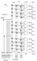
図3はワード線デコーダ300の回路図である。図3の実施例において、ワード線デコーダ300は32のワード線WL[0]、...、WL[31](総称してWL)を有するが、別の数のワード線が同様に使用されてもよい。デコード線DEA[0]、DEA[1]、DEB[0]、DEB[1]が図3のように使用される場合、デコード線が2ビットの情報を提供して22(すなわち、4)のワード線を選択するので、最低4本のワード線が使用される。ドライバ310−0、310−1、...、310−31(総称して310)にはワード線WLが設けられ、そしてドライバ310はクラスタ320−0、...、320−7(総称して320)内に配置される。図3の実施例において、各クラスタ320は4つのドライバ310を有し、結果として8つのクラスタとなる。しかしながら、異なる数のクラスタを使用してもよい。FIG. 3 is a circuit diagram of the
各ドライバ310は3本の入力線を有するが、それは論理ANDゲートであってよい。ドライバ310−0の場合、SA0およびSB0と表示された入力線のうちの2本は、2次入力線と呼ばれる。2次入力線はデコード線DEA[0]、DEA[1]、DEB[0]およびDEB[1]に接続されるが、それらは補助デコード線と呼ばれる。クラスタ、例えば、クラスタ320−0の中で、第2のデコード線と共に補助デコード線が特定のドライバ310を決定する。例えば、クラスタ320―0では、補助デコード線DEA[0]、DEA[1]、DEB[0]、DEB[1]は、4つのドライバ310−0,310−1,310−2,310−3のうちの1つを選択する、2ビットの情報を供給する。各ドライバ310への3本目の入力線は、主入力線として知られている。ドライバ310−0、...、310−31への主入力線は、図3でP0、...、P31と表記される。主および2次入力線は第1の方向に配向され、それは図3の実施例で水平線と称してもよい。当該クラスタでは、クラスタの中のドライバ310への主入力線の全ては、第1の方向に対して垂直な第2の方向に配向されたローカル・デコード線を介して、共に接続される。第2の方向は、図3の実施例において、垂直と称してもよい。「水平」および「垂直」の用語は互いに相対的なものであることは理解されるべきである。ローカル・デコード線は、クラスタ320に対応する末尾番号を有する参照符号により表記される。例えば、クラスタ320−7の主入力線に接続するローカル・デコード線はVLOCDEC7と表記され、ここで接頭語「V」は便宜上垂直を示す。 Each driver 310 has three input lines, but it may be a logical AND gate. For driver 310-0, two of the input lines labeled SA0 and SB0 are called secondary input lines. Secondary input lines are connected to decode lines DEA [0], DEA [1], DEB [0] and DEB [1], which are called auxiliary decode lines. Within a cluster, eg, cluster 320-0, the auxiliary decode line along with the second decode line determines a particular driver 310. For example, in the cluster 320-0, the auxiliary decode lines DEA [0], DEA [1], DEB [0], DEB [1] are four drivers 310-0, 310-1, 310-2, 310-3. 2 bits of information are supplied to select one of the two. The third input line to each driver 310 is known as the main input line. Drivers 310-0,. . . , 310-31 are labeled P0,. . . , P31. The primary and secondary input lines are oriented in a first direction, which may be referred to as a horizontal line in the embodiment of FIG. In the cluster, all of the main input lines to the driver 310 in the cluster are connected together via local decode lines oriented in a second direction perpendicular to the first direction. The second direction may be referred to as vertical in the embodiment of FIG. It should be understood that the terms “horizontal” and “vertical” are relative to each other. The local decode line is represented by a reference sign having a tail number corresponding to the cluster 320. For example, the local decode line connected to the main input line of cluster 320-7 is denoted as VLOCDEC7, where the prefix “V” indicates vertical for convenience.
各ローカル・デコード線は、ローカル・デコード線と垂直に交差するデコード線に接続され、後者のデコード線は便宜上水平デコード線と称することができ、接頭語「H」で表記されうる。例えば、水平デコード線HDEC7はローカル・デコード線VLCDEC7に接続される。用語「水平」は相対的で、水平デコード線が駆動回路310に入力線と同じ方向に配向されることを示すこと、と理解されるべきである。各水平デコード線は、ローカル・デコード線(すなわち、水平デコード線と直角をなす)と同方向に配向されるクラスタ・デコード線に接続される。クラスタ・デコード線DEC[0]、...、DEC[7]は、各クラスタ・デコード線が対応するクラスタを選択するので、そのように名づけられる。例えば、クラスタ・デコード線DEC[0]は、クラスタ320−0を選択するが、それは、クラスタ・デコード線DEC[0]は、それぞれ主入力線P0、P1、P2、P3を通してクラスタ320−0の駆動回路310−0、310−1、310−2、310−3の各々に、ローカル・デコード線VLOCDEC0を介して接続されるから、である。 Each local decode line is connected to a decode line that intersects perpendicularly with the local decode line, and the latter decode line can be referred to as a horizontal decode line for convenience and can be denoted by a prefix “H”. For example, the horizontal decode line HDEC7 is connected to the local decode line VLCDEC7. It should be understood that the term “horizontal” is relative and indicates that the horizontal decode line is oriented to the drive circuit 310 in the same direction as the input line. Each horizontal decode line is connected to a cluster decode line that is oriented in the same direction as the local decode line (ie, perpendicular to the horizontal decode line). Cluster decode lines DEC [0],. . . , DEC [7] are so named because each cluster decode line selects the corresponding cluster. For example, the cluster decode line DEC [0] selects the cluster 320-0, and the cluster decode line DEC [0] is connected to the cluster 320-0 through the main input lines P0, P1, P2, and P3, respectively. This is because the drive circuits 310-0, 310-1, 310-2, and 310-3 are connected to each other via the local decode line VLOCDEC0.
各種の実施形態は図3に示される特徴の異なる組み合わせ(部分集合)を有してもよいが、図3に示されるワード線デコーダ300の具体例と従来のワード線デコーダ200との間にはいくつかの差異がある。各クラスタ・デコード線は、その対応するクラスタに接続するのに、すなわち、その対応する水平デコード線との相互接続部までに十分な距離を延びるだけなので、ワード線デコーダ300においては(デコーダ200より)少ない回路でよい。例えば、クラスタ・デコード線DEC[0]は、ワード線デコーダ300の基端に近いところからからクラスタ320―0に付随する水平デコード線まで、またはその水平デコード線を過ぎたわずかな距離だけ、すなわち、ワード線デコーダ300の末端にまでずっとということではなく、水平デコード線HDEC0まで、あるいはそれをわずかに過ぎたところまで延びる。ここで、用語「末端」および「基端」は、クラスタ320−0(第1のクラスタ)および320−31(最後のクラスタ)がそれぞれ設けられたワード線デコーダ300の端に対応する。従来のワード線デコーダ200は、ワード線デコーダ300とは対照的に、対応するクラスタの駆動回路の全てに接続される単一の水平デコード線を備えていない。各クラスタのための単一の水平デコード線によって、ワード線デコーダ300は、ワード線デコーダ200に対して水平方向(上記のように、用語「水平」は相対的)の回路を減じる。例えば、クラスタ320−7のために、ワード線デコーダ300は、Xと表示されうる長さを有する4本の主入力線と、Yで表示されうる長さを有する1本の水平デコード線、そして全体の長さ4X+Yを有する。対照的に、サービス駆動回路310−28,310−29、310−30および310−31について、従来のワード線デコーダは、各々長さ(X+Y)を有する4本の入力線を必要とし、全体の長さは4X+4Yとなる。ローカル・デコード線、例えばVLOCDEC0、はデバイスの近くに配置されることができ、従来技術を超えた更なる優位性を備える。 Various embodiments may have different combinations (subsets) of the features shown in FIG. 3, but between the specific example of the
クラスタ・デコード線DEC[0]、...、DEC[7]は、図3では特定の序列で配置される。すなわちこの序列は、図4Aにより理解されうる。図4A乃至図4Cは、各種実施形態のワード線デコーダのクラスタ・デコード線のレイアウトの回路図であり、そして、図4Aは結合容量および抵抗を最小化する実施例のレイアウトを示す。図4Aでは、クラスタ・デコード線は、左から右への序列で、DEC[0]、DEC[7]、DEC[1]、DEC[6]、DEC[2]、DEC[5]、DEC[3]、DEC[4]として、すなわち、一番遠くから最も近くのドライバ(例えば、ANDゲート)へ配置される。便宜上、この配置は、0−7−1−6−2−5−3−4と表示してよい。したがって、最も短いクラスタ・デコード線DEC[0](すなわち、ワード線デコーダの基端のクラスタに対応するクラスタ・デコード線)は、最も長いクラスタ・デコード線DEC[7]と隣接しており、したがって、2つの間の重複を最小化し、金属負荷を減らすことによって、結合容量を最小化する。加えて、従来技術と比較してクラスタ・デコード線DEC[0]の長さを減らすことにより、抵抗(それは線の長さに直接関連する)は、同様に最小化される。図4Aのようなクラスタ・デコード線の0−7−1−6−2−5−3−4配置は、以下の数学的定式化で表されうる方法で、結合容量を最小化する。この配置は、クラスタ・デコード線全体に亘り、隣接するクラスタ・デコード線間の長さの差分の大きさの合計を最大にする。換言すれば、|L(0)−L(7)|+|L(7)−L(1)|+|L(1)−L(6)|+|L(6)−L(2)|+|L(2)−L(5)|+|L(5)−L(3)|+|L(3)−L(4)|の合計は、隣接するクラスタ・デコード線の長さの差分(絶対値)の、クラスタ・デコード線全体に亘るすべての可能な合計の、最大である。ここでL(i)はDEC[i]の長さを意味する。別の言い方をすれば、クラスタ・デコード線は、各対の隣接するクラスタ・デコード線との重複の合計が最小となるよう配置される。上記の合計最大化の属性を満足する他の配置は、例えば4−3−5−2−6−1−7−0(上記の配置の反対)、7−0−6−1−5−2−4−3および3−4−2−5−1−6−0−7である。当業者であれば、クラスタ・デコード線の配置の同じ判定基準がいかなる所与の数のクラスタへも、そしてクラスタ当たりのいかなる所与の数のドライバへも拡張できる、ことが分かる。 Cluster decode lines DEC [0],. . . , DEC [7] are arranged in a specific order in FIG. That is, this ordering can be understood from FIG. 4A. 4A-4C are circuit diagrams of the layout of the cluster decode lines of the word line decoders of various embodiments, and FIG. 4A shows an example layout that minimizes coupling capacitance and resistance. In FIG. 4A, the cluster decode lines are arranged from left to right in the order of DEC [0], DEC [7], DEC [1], DEC [6], DEC [2], DEC [5], DEC [ 3], DEC [4], that is, from the farthest to the nearest driver (for example, an AND gate). For convenience, this arrangement may be denoted as 0-7-1-6-2-5-3-4. Therefore, the shortest cluster decode line DEC [0] (that is, the cluster decode line corresponding to the base cluster of the word line decoder) is adjacent to the longest cluster decode line DEC [7], and therefore Minimize the coupling capacity by minimizing the overlap between the two and reducing the metal load. In addition, by reducing the length of the cluster decode line DEC [0] compared to the prior art, the resistance (which is directly related to the length of the line) is minimized as well. The cluster decode line 0-7-1-6-2-5-3-4 arrangement as in FIG. 4A minimizes the coupling capacitance in a manner that can be expressed in the following mathematical formulation. This arrangement maximizes the sum of the length differences between adjacent cluster decode lines across the cluster decode lines. In other words, | L (0) −L (7) | + | L (7) −L (1) | + | L (1) −L (6) | + | L (6) −L (2) | + | L (2) −L (5) | + | L (5) −L (3) | + | L (3) −L (4) | is the sum of the lengths of adjacent cluster decode lines. Of the difference (absolute value) of all possible sums across the entire cluster decode line. Here, L (i) means the length of DEC [i]. In other words, the cluster decode lines are arranged such that the sum of overlap with each pair of adjacent cluster decode lines is minimized. Other arrangements that satisfy the above-mentioned total maximization attribute are, for example, 4-3-5-2-2-6-1-7-0 (opposite of the above arrangement), 7-0-6-1-5-2. -4-3 and 3-4-2-2-5-1-6-0-7. One skilled in the art will appreciate that the same criteria for placement of cluster decode lines can be extended to any given number of clusters and to any given number of drivers per cluster.
32本のワード線が図3および図4A乃至図Cに示されているが、上述のように、別の数のワード線が使用されてもよい。例えば、128本または512本のワード線が使用されうる。例えば、128本のワード線の場合、3ビットの情報を供給するクラスタ・デコード線DEC[0]、…、DEC[7]は8つの(すなわち23)クラスタの間で選択することができ、各々のクラスタは16のドライバを有し、それらは、適当な補助デコード線を介して選択されうる。同様に、512本のワード線のためには、8本のクラスタ・デコード線は、各々64のドライバを有する8つのクラスタ間で選択できる。ワード線の数がより大きくなれば、(従来技術に比較して)より多くの利点が達成される。補助デコード線およびクラスタ・デコード線の配置、そして、ドライバへの異なる入力線間の補助デコード線の相対的な配置は、当業者が理解すべきものとして、特定の実装の過程で調整されうる。Thirty-two word lines are shown in FIGS. 3 and 4A-C, but as described above, other numbers of word lines may be used. For example, 128 or 512 word lines can be used. For example, in the case of 128 word lines, the cluster decode lines DEC [0],..., DEC [7] supplying 3 bits of information can be selected between 8 (ie 23 ) clusters, Each cluster has 16 drivers, which can be selected via appropriate auxiliary decode lines. Similarly, for 512 word lines, eight cluster decode lines can be selected between eight clusters each having 64 drivers. More advantages are achieved (as compared to the prior art) as the number of word lines is increased. The placement of the auxiliary decode lines and cluster decode lines, and the relative placement of the auxiliary decode lines between different input lines to the driver, as should be understood by those skilled in the art, can be adjusted in the course of a particular implementation.
図4Bおよび図4Cに示すように、別の配置では、クラスタ・デコード線を、長さを減少するかまたは増加することによって、配置できる。これらの配置は、以下の数式により表されうる:P(p)=p!、ここでp!=1x2x3x...(p−1)xp。符号pはクラスタ・デコード線の数である。これらの配置は、クラスタ・デコード線全体に、隣接するクラスタ・デコード線間の長さの差異の大きさの合計を最小化する(上記のように最大化するのではなく)。クラスタ・デコード線の他のいかなる配置も、同様に可能であり、すなわち、p!配置のいずれもが、pクラスタ・デコード線の場合に使用されうる。 In another arrangement, as shown in FIGS. 4B and 4C, the cluster decode lines can be arranged by decreasing or increasing the length. These arrangements can be represented by the following formula: P (p) = p! Here, p! = 1x2x3x. . . (P-1) xp. The symbol p is the number of cluster decode lines. These arrangements minimize (rather than maximize) the overall magnitude of the length difference between adjacent cluster decode lines across the cluster decode lines. Any other arrangement of cluster decode lines is possible as well, ie p! Any of the arrangements can be used for p-cluster decode lines.
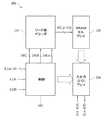
図5は、メモリ・システムのブロック図である。メモリ・システム500は、ワード線デコーダ510、SRAMセル・アレイ520、入出力(I/O)アレイ530および制御ロジック540を備える。図5は、SRAMブロックの表面の図を提供するものと見なしてもよい。ワード線デコーダ510は、図3のワード線デコーダ300、または異なる数のデコード線および/またはワード線を有する同様のワード線デコーダであってもよい。ワード線デコーダ500は、SRAMセル・アレイ520のnビットセルをアドレスするnワード線を有するものとして、図5に示されている。I/Oアレイ530は、SRAMセル・アレイ520に対してデータを書き込む(図5のDで示す)またはそれからデータを読出す(図5のQで示す)ための、従来技術において、知られた通常の入出力アレイか、またはこれらの機能を有する、将来開発されるI/Oアレイであってよい。制御ロジック540は、アドレス(図5でmビットからなるものとして示された)、クロック信号、そしてSRAMセル・アレイ520へ/からのアクセス、読出し/書込みを制御するための、チップ・イネーブル信号CEBを受信する。制御ロジック540は、アドレスA[m−l:0]を、デコード線DEAおよびDEB(上記の補助デコード線)およびDEC(上記のクラスタ・デコード線)に供給されるデコード信号に翻訳する。ワード線デコーダは図5ではワード線ドライバ・アレイと呼ばれる。 FIG. 5 is a block diagram of the memory system. The
図6は、メモリ・システムのストラップ・セル構成のブロック図である。当業者には知られているように、SRAMストラップ・セルは、P−ウェルそしてN−ウェルに対するバイアス電圧を低下させるために、SRAMセル・アレイに埋め込まれて使用されるスタンダードセルである。P−ウェル(P型基板)およびN−ウェル・バイアスは、それぞれ、NMOSおよびPMOSデバイスのバルク(本体とも呼ばれる)である。 FIG. 6 is a block diagram of the strap cell configuration of the memory system. As known to those skilled in the art, an SRAM strap cell is a standard cell that is used embedded in an SRAM cell array to reduce the bias voltage for the P-well and N-well. P-well (P-type substrate) and N-well bias are the bulk (also called body) of NMOS and PMOS devices, respectively.
SRAMストラップ・セルは、各固定数のSRAMセル(ビットセル)に、すなわち、kビットセルごとに配置されることができる。図6において、ワード線ストラップ・セル632は、隣接する、64の列およびColカラムを有するSRAMセル・アレイ620a、620bと隣接した、64x1ワード線ドライバ・アレイ(ワード線デコーダ)610a、610bの間に設けられる。1つの列およびColカラムを有するSRAMストラップ・セル・アレイは、SRAMセル・アレイ620aと620bとの間に設けられる。SRAMセル・アレイの列の最大許容数はウェル・バイアス(well bias)から一番遠いSRAMセルまでの最大距離により制限され、65nmCMOS製造工程のための設計仕様によると、それは典型的には約30μmである。図3のような水平デコード線(例えば、HDEC0)は、ストラップ・セル632中に、またはSRAMストラップ・セル・アレイ634中に実装されうる。あるいは、水平デコード線は、図7の説明の中で後述するローカル制御ロジック中に実装されうる。 An SRAM strap cell can be placed in each fixed number of SRAM cells (bit cells), ie, every k bit cells. In FIG. 6, a word
図7は、メモリ・バンクのアレイのブロック図である。メモリ・バンク710−0、710−1は、図5のメモリ・システム500と同様な構造である。メモリ・バンク1は、SRAMセル・アレイ720、ワード線ドライバ・アレイ710、ローカル制御ロジック742、ローカル入出力(LIO)アレイ732、I/Oアレイ730および主制御部740を有する。主制御部740は、図3に示すようなデコード信号DEC[0]、DEC[1]、DEC[2]およびDEC[3]を供給する。他のデコード信号は図7に示されていない。ローカル制御部742は、ローカル読出し回路またはローカル書込みデータバッファのように、読出し及び書込みを行うためLIOアレイ732を制御する。ローカル読出し回路は、図1の信号BLとBL_INVとの間の電圧差を検出するための差動増幅器を含むことができる。水平デコード線は、金属ピッチのための充分な金属スペースがあるどの位置においても、ローカル制御部742を通過できる。各種の実施形態がテストされてきており、従来技術のワード線デコーダに対して、結合容量の減少、抵抗の減少、電源消費の減少およびより良いタイミング性能(より速いアクセス)を示している。表1は128本のワード線をもつ実施態様での結合容量の減少を示す。
表2は、実施態様の32Kbレジスタ・ファイルのための向上したタイミング性能(アクセス時間)を示す。
実施例が示され、記載されているにもかかわらず、さまざまな変形および構造変更が、請求項と均等の範囲内で当業者によりなされうるので、実施態様は示された詳細に限定されない。 Although the embodiments have been shown and described, the embodiments are not limited to the details shown, since various modifications and structural changes may be made by those skilled in the art within the scope of the claims.
100 SRAMメモリーセル
110 NMOSトランジスタ
120 PMOSトランジスタ
130 NMOSトランジスタ
140 PMOSトランジスタ
150、160 NMOSトランジスタ
BL、BL_INV ビット線
WL ワード線
200 ワード線デコーダ
210 ドライバ
DEA デコード線
300 ワード線デコーダ
310 ドライバ
320 クラスタ
VLOCDEC ローカル・デコード線
HDEC 水平デコード線
DEC クラスタ・デコード線
500 メモリ・システム
510 ワード線デコーダ
520 SRAMセル・アレイ
530 入出力(I/O)アレイ
540 制御ロジック
610 ワード線ドライバ・アレイ
620 SRAMセル・アレイ
710 メモリ・バンク
720 SRAMセル・アレイ
710 ワード線ドライバ・アレイ
742 ローカル制御ロジック
732 ローカル入出力(LIO)アレイ
730 I/Oアレイ
740 主制御部
742 ローカル制御部
100
Claims (7)
Translated fromJapanese当該ドライバのそれぞれの出力に設けられた複数のワード線と、
当該ドライバに接続された複数の主入力線であって、当該主入力線は第1の方向に配向されるものと、
当該ドライバに接続される複数の2次入力線であって、当該2次入力線は第1の方向に配向されるものと、
当該主入力線の各々に接続されるローカル・デコード線と、
当該ローカル・デコード線に接続されるデコード線であって、当該デコード線は第1の方向に配向されるものと、そして
当該デコード線に接続されるクラスタ・デコード線とからなり、
当該クラスタ・デコード線および当該2次入力線により供給される信号に基づき、当該ワード線のうちの少なくとも1を選択するよう構成され、
前記各クラスタ・デコード線は、前記第1の方向に対して垂直な第2の方向に配向され、対応する前記デコード線の相互接続点で、またはそれを越えたわずかな距離で終端するよう形成され、前記各デコード線は、対応する前記ローカル・デコード線の基端に接続され、最も長い前記クラスタ・デコード線は、最も短い前記クラスタ・デコード線の隣に設けられ、そして前記クラスタ・デコード線は、前記クラスタ・デコード線全体に、隣接する前記クラスタ・デコード線間の長さの差異の大きさの総和を最大にするよう配置される
ワード線デコーダ。Multiple drivers,
A plurality of word lines provided at respective outputs of the driver;
A plurality of main input lines connected to the driver, wherein the main input lines are oriented in a first direction;
A plurality of secondary input lines connected to the driver, wherein the secondary input lines are oriented in a first direction;
A local decode line connected to each of the main input lines;
A decode line connected to the local decode line, the decode line being oriented in a first direction, and a cluster decode line connected to the decode line;
Based on a signal supplied by the cluster decode line and the secondary input line, configured to select at least one of the word lines;
Each cluster decode line is oriented in a second direction perpendicular to the first direction and is formed to terminate at or slightly beyond the corresponding interconnect point of the decode lines Each decode line is connected to a base end of the corresponding local decode line, the longest cluster decode line is provided next to the shortest cluster decode line, and the cluster decode line Is a word line decoderarranged to maximize the total sum of the length differences between adjacent cluster decode lines over the entire cluster decode line .
全体でNの追加のドライバ・クラスタと、
全体でNの追加のローカル・デコード線であって、各々が対応する前記ドライバ・クラスタの当該主入力線に接続されるものと、
全体でNの追加のデコード線であって、各々が対応する前記ローカル・デコード線に接続されるものと、
全体でNの追加のクラスタ・デコード線であって、各々が対応する前記デコード線に接続されるもの
からなる請求項1に記載のワード線デコーダ。The driver, the main input line and the secondary input line define a first driver cluster; and
A total of N additional driver clusters;
A total of N additional local decode lines, each connected to the main input line of the corresponding driver cluster;
A total of N additional decode lines, each connected to the corresponding local decode line;
2. The word line decoder according to claim 1, comprising a total of N additional cluster decode lines, each connected to the corresponding decode line.
複数のデータ・ビットを記憶するように構成された複数のスタティック・ランダム・アクセス・メモリ(SRAM)セルであって、各セルは対応するワード線によって、アクティブにされるものと、
それぞれ、第1および第2の複数のデコード線に第1および第2の複数のデコード信号を供給するように構成された制御ロジックと、
当該制御ロジックからの入力信号に基づいて当該データ・ビットを読出し及び書込みするように構成された入出力アレイと、そして
ワード線デコーダであって、
複数のドライバ・クラスタ、各当該ドライバ・クラスタは
複数のドライバ(駆動回路)、各当該ドライバの出力は対応する当該ワード線に供給されるもの、
複数のローカル・デコード線、各当該ローカル・デコード線は第1の方向に配向された対応する複数の入力線を介して、対応する当該ドライバ・クラスタの当該ドライバに接続されたもの、そして
第1の方向において、配向される第3の複数のデコード線、当該デコード線の各々は対応する当該ローカル・デコード線と、前記第1の複数のデコード線のうちの1に接続されるものとをふくむワード線デコーダと
からなり、
前記第1の複数のデコード線の各々は、第1の方向に対して垂直な第2の方向に配向され、前記第3の複数のデコード線の対応する一つの相互接続点で、またはそれを過ぎたわずかな距離で終端するよう構成され、そして前記第3の複数のデコード線の各々は、最も近い対応するローカル・デコード線の基端に接続され、前記第1の複数のデコード線のうちの最も長い1つは、前記第1の複数のデコード線のうちの最も短い1つに、隣り合って設けられ、そして前記第1の複数のデコード線は、前記第1の複数のデコード線の全体に、前記第1の複数のデコード線の隣接するものの長さの差異の大きさの総和を最大にするよう配置される
メモリ素子。Multiple word lines,
A plurality of static random access memory (SRAM) cells configured to store a plurality of data bits, each cell being activated by a corresponding word line;
Control logic configured to provide first and second plurality of decode signals to the first and second plurality of decode lines, respectively;
An input / output array configured to read and write the data bits based on input signals from the control logic, and a word line decoder,
A plurality of driver clusters, each driver cluster is a plurality of drivers (drive circuits), and the output of each driver is supplied to the corresponding word line;
A plurality of local decode lines, each of the local decode lines connected to the driver of the corresponding driver cluster via a corresponding input line oriented in a first direction; and In this direction, each of the third plurality of decode lines to be oriented includes each of the corresponding decode lines connected to the corresponding local decode line and one of the first plurality of decode lines. word line decoder andRi Tona,
Each of the first plurality of decode lines is oriented in a second direction perpendicular to the first direction, at or corresponding to a corresponding interconnection point of the third plurality of decode lines. Each of the third plurality of decode lines is connected to a proximal end of the nearest corresponding local decode line, and is configured to terminate the first plurality of decode lines. The longest one of the first plurality of decode lines is provided adjacent to the shortest one of the first plurality of decode lines, and the first plurality of decode lines are the first plurality of decode lines. Overall, the first plurality of decode lines are arranged so as to maximize the sum of the length differences between adjacent ones of the plurality of decode lines.
Memory element.
第1の方向に配向する複数の入力線を備え、
複数のローカル・デコード線を備え、当該各ローカル・デコード線は、対応する当該入力線を経て、対応する当該ドライバ・クラスタの当該ドライバに接続され、そして、
第1の方向において、配向される第3の複数のデコード線を備え、当該第3の複数の各デコード線は、対応する当該ローカル・デコード線と当該第1の複数のデコード線のうちの1つとに接続され、
前記第1の複数のデコード線の各々は、第1の方向に対して垂直な第2の方向に配向され、前記第3の複数のデコード線の対応する一つの相互接続と、あるいはそれを過ぎたわずかな距離で終端するよう構成され、前記第3の複数のデコード線の各々は、対応する前記ローカル・デコード線の基端に接続され、そして前記第1の複数のデコード線うちの最も長い1つは、前記第1の複数デコード線のうちの最も短い1つに、隣り合って設けられる
回路のレイアウトを構成する方法。A plurality of driver clusters, each driver cluster comprising a plurality of drivers, and an output of each driver is supplied to the corresponding word line among the plurality of word lines; The first plurality of decode signals are respectively supplied to the decode lines, and the first plurality of decode lines are configured to select one of the driver clusters, and the second plurality of decode lines are selected. Is configured to select one of the drivers in the selected driver cluster,
Comprising a plurality of input lines oriented in a first direction;
A plurality of local decode lines, each local decode line being connected to the corresponding driver in the corresponding driver cluster via the corresponding input line; and
A third plurality of decode lines oriented in a first direction, wherein each of the third plurality of decode lines is one of the corresponding local decode line and the first plurality of decode lines; early in lifeare connected,
Each of the first plurality of decode lines is oriented in a second direction that is perpendicular to the first direction, and corresponding to or past one corresponding interconnect of the third plurality of decode lines. Each of the third plurality of decode lines is connected to a proximal end of the corresponding local decode line, and is the longest of the first plurality of decode lines. One is provided adjacent to the shortest one of the first plurality of decode lines.
How to configure the layout of a circuit.
Applications Claiming Priority (2)
| Application Number | Priority Date | Filing Date | Title |
|---|---|---|---|
| US12/839,490 | 2010-07-20 | ||
| US12/839,490US8837250B2 (en) | 2010-07-20 | 2010-07-20 | Method and apparatus for word line decoder layout |
Publications (2)
| Publication Number | Publication Date |
|---|---|
| JP2012027999A JP2012027999A (en) | 2012-02-09 |
| JP5289469B2true JP5289469B2 (en) | 2013-09-11 |
Family
ID=45493531
Family Applications (1)
| Application Number | Title | Priority Date | Filing Date |
|---|---|---|---|
| JP2011007334AActiveJP5289469B2 (en) | 2010-07-20 | 2011-01-17 | Method and apparatus for word line decoder layout |
Country Status (3)
| Country | Link |
|---|---|
| US (1) | US8837250B2 (en) |
| JP (1) | JP5289469B2 (en) |
| CN (1) | CN102339639B (en) |
Families Citing this family (3)
| Publication number | Priority date | Publication date | Assignee | Title |
|---|---|---|---|---|
| EP3710013B1 (en) | 2017-11-15 | 2025-07-30 | Weird Science LLC | Methods and compositions for non-myeloablative bone marrow reconstitution |
| DE102019128331B4 (en) | 2019-08-29 | 2024-10-02 | Taiwan Semiconductor Manufacturing Co., Ltd. | SHARED DECODER CIRCUIT AND METHOD |
| CN112447218B (en) | 2019-08-29 | 2025-05-06 | 台湾积体电路制造股份有限公司 | Memory circuit and method |
Family Cites Families (14)
| Publication number | Priority date | Publication date | Assignee | Title |
|---|---|---|---|---|
| US5652723A (en)* | 1991-04-18 | 1997-07-29 | Mitsubishi Denki Kabushiki Kaisha | Semiconductor memory device |
| JP3108505B2 (en) | 1992-03-13 | 2000-11-13 | 沖電気工業株式会社 | Decoder circuit |
| KR0164823B1 (en) | 1995-04-27 | 1999-02-01 | 김광호 | Memory operating in high speed |
| JP4398551B2 (en)* | 1998-12-25 | 2010-01-13 | 株式会社東芝 | Semiconductor device |
| JP2001222463A (en)* | 2000-02-10 | 2001-08-17 | Hitachi Ltd | Memory device |
| US6275442B1 (en)* | 2000-05-16 | 2001-08-14 | Hewlett-Packard Company | Address decoder and method for ITS accelerated stress testing |
| JP5431624B2 (en) | 2000-05-30 | 2014-03-05 | ピーエスフォー ルクスコ エスエイアールエル | Semiconductor memory device |
| JP3639241B2 (en) | 2001-10-11 | 2005-04-20 | 株式会社東芝 | Semiconductor device |
| US6909648B2 (en)* | 2002-03-19 | 2005-06-21 | Broadcom Corporation | Burn in system and method for improved memory reliability |
| JP4498088B2 (en) | 2004-10-07 | 2010-07-07 | 株式会社東芝 | Semiconductor memory device and manufacturing method thereof |
| US7215587B2 (en) | 2005-07-05 | 2007-05-08 | Taiwan Semiconductor Manufacturing Company, Ltd. | Tracking circuit for a memory device |
| JP2007019997A (en) | 2005-07-08 | 2007-01-25 | Sony Corp | Field-effect transistor circuit and designing method |
| JP4749089B2 (en) | 2005-08-26 | 2011-08-17 | ルネサスエレクトロニクス株式会社 | Semiconductor device |
| JP2010257552A (en) | 2009-04-28 | 2010-11-11 | Elpida Memory Inc | Semiconductor storage device |
- 2010
- 2010-07-20USUS12/839,490patent/US8837250B2/enactiveActive
- 2010-11-05CNCN201010538947.XApatent/CN102339639B/enactiveActive
- 2011
- 2011-01-17JPJP2011007334Apatent/JP5289469B2/enactiveActive
Also Published As
| Publication number | Publication date |
|---|---|
| CN102339639B (en) | 2014-01-01 |
| US20120020179A1 (en) | 2012-01-26 |
| US8837250B2 (en) | 2014-09-16 |
| CN102339639A (en) | 2012-02-01 |
| JP2012027999A (en) | 2012-02-09 |
Similar Documents
| Publication | Publication Date | Title |
|---|---|---|
| US10354719B2 (en) | 3D structure for advanced SRAM design to avoid half-selected issue | |
| US7483332B2 (en) | SRAM cell using separate read and write circuitry | |
| US9646681B1 (en) | Memory cell with improved write margin | |
| US7403426B2 (en) | Memory with dynamically adjustable supply | |
| US7313050B2 (en) | Word-line driver for memory devices | |
| US9001546B2 (en) | 3D structure for advanced SRAM design to avoid half-selected issue | |
| US20110103137A1 (en) | Source controlled sram | |
| US20100165704A1 (en) | Circuit and Method for a High Speed Memory Cell | |
| US20030193824A1 (en) | Semiconductor memory device | |
| CN100593824C (en) | SRAM cell array and integrated circuit structure | |
| US20070183234A1 (en) | Semiconductor memory device having reduced voltage coupling between bit lines | |
| US9881655B2 (en) | Memory circuit having data lines selectively coupled to a sense amplifier and method for operating the same | |
| US9305635B2 (en) | High density memory structure | |
| JP3889848B2 (en) | Semiconductor memory device | |
| JP5289469B2 (en) | Method and apparatus for word line decoder layout | |
| CN112530479A (en) | Low cell voltage charge sharing circuit | |
| JP2012195038A (en) | Semiconductor storage device | |
| US20110235447A1 (en) | Low power memory array column redundancy mechanism | |
| CN104637528B (en) | SRAM memory cell array, SRAM memory and its control method | |
| US20250087293A1 (en) | Memory module, operating method of memory module, and memory system including memory module | |
| JP4420919B2 (en) | Semiconductor memory device | |
| US20080123437A1 (en) | Apparatus for Floating Bitlines in Static Random Access Memory Arrays | |
| JP2008065863A (en) | Semiconductor memory device | |
| JP2010067309A (en) | Semiconductor memory device |
Legal Events
| Date | Code | Title | Description |
|---|---|---|---|
| RD04 | Notification of resignation of power of attorney | Free format text:JAPANESE INTERMEDIATE CODE: A7424 Effective date:20111115 | |
| A977 | Report on retrieval | Free format text:JAPANESE INTERMEDIATE CODE: A971007 Effective date:20121105 | |
| A131 | Notification of reasons for refusal | Free format text:JAPANESE INTERMEDIATE CODE: A131 Effective date:20121120 | |
| A521 | Request for written amendment filed | Free format text:JAPANESE INTERMEDIATE CODE: A523 Effective date:20130220 | |
| TRDD | Decision of grant or rejection written | ||
| A01 | Written decision to grant a patent or to grant a registration (utility model) | Free format text:JAPANESE INTERMEDIATE CODE: A01 Effective date:20130507 | |
| A61 | First payment of annual fees (during grant procedure) | Free format text:JAPANESE INTERMEDIATE CODE: A61 Effective date:20130604 | |
| R150 | Certificate of patent or registration of utility model | Ref document number:5289469 Country of ref document:JP Free format text:JAPANESE INTERMEDIATE CODE: R150 | |
| R250 | Receipt of annual fees | Free format text:JAPANESE INTERMEDIATE CODE: R250 | |
| R250 | Receipt of annual fees | Free format text:JAPANESE INTERMEDIATE CODE: R250 | |
| R250 | Receipt of annual fees | Free format text:JAPANESE INTERMEDIATE CODE: R250 | |
| R250 | Receipt of annual fees | Free format text:JAPANESE INTERMEDIATE CODE: R250 | |
| R250 | Receipt of annual fees | Free format text:JAPANESE INTERMEDIATE CODE: R250 | |
| R250 | Receipt of annual fees | Free format text:JAPANESE INTERMEDIATE CODE: R250 | |
| R250 | Receipt of annual fees | Free format text:JAPANESE INTERMEDIATE CODE: R250 | |
| R250 | Receipt of annual fees | Free format text:JAPANESE INTERMEDIATE CODE: R250 | |
| R250 | Receipt of annual fees | Free format text:JAPANESE INTERMEDIATE CODE: R250 | |
| R250 | Receipt of annual fees | Free format text:JAPANESE INTERMEDIATE CODE: R250 |