JP5287286B2 - Bias circuit - Google Patents
Bias circuitDownload PDFInfo
- Publication number
- JP5287286B2 JP5287286B2JP2009011321AJP2009011321AJP5287286B2JP 5287286 B2JP5287286 B2JP 5287286B2JP 2009011321 AJP2009011321 AJP 2009011321AJP 2009011321 AJP2009011321 AJP 2009011321AJP 5287286 B2JP5287286 B2JP 5287286B2
- Authority
- JP
- Japan
- Prior art keywords
- node
- impedance
- bias circuit
- impedance conversion
- inductive element
- Prior art date
- Legal status (The legal status is an assumption and is not a legal conclusion. Google has not performed a legal analysis and makes no representation as to the accuracy of the status listed.)
- Expired - Fee Related
Links
Images


Landscapes
- Waveguide Connection Structure (AREA)
- Microwave Amplifiers (AREA)
Description
Translated fromJapanese本発明は、商用通信機や軍事用レーダーのような広帯域アプリケーションで使用される高出力増幅器等に用いられるバイアス回路に関する。 The present invention relates to a bias circuit used for a high-power amplifier or the like used in a broadband application such as a commercial communication device or a military radar.
特開平9−214201号公報には、主線路を伝播する高周波信号の通過特性に影響を与えないでスイッチング素子にDCバイアス電圧を印加する高周波バイアス回路において、前記主線路と接する第一の高インピーダンス線路の他端に設け高周波帯で十分低いインピーダンスをもつ第2のキャパシタを介し接地する第2の高インピーダンス線路と第1のキャパシタからなる並列共振回路で、所望周波数帯の下限周波数近傍では前記第1と第2の高インピーダンス線路を足し合わせたときの位相変化がλ/4波長に相当し且つ第一のキャパシタの持つインピーダンスが十分高くなり、上限周波数近傍では共振するように設定することを特徴とする高周波バイアス回路が開示されている。 Japanese Patent Laid-Open No. 9-214201 discloses a first high-impedance contact with the main line in a high-frequency bias circuit that applies a DC bias voltage to the switching element without affecting the passage characteristics of the high-frequency signal propagating through the main line. A parallel resonant circuit comprising a first capacitor and a second high impedance line provided at the other end of the line and grounded via a second capacitor having a sufficiently low impedance in the high frequency band, in the vicinity of the lower limit frequency of the desired frequency band. The phase change when adding the first and second high impedance lines corresponds to λ / 4 wavelength, the impedance of the first capacitor is sufficiently high, and the resonance is set near the upper limit frequency. A high frequency bias circuit is disclosed.
また、特開2006−80698号公報には、半導体増幅素子を用いた直列帰還形の高周波発振回路を用いた周波数変換方法であって、線路の電気長が1波長であるマイクロストリップ線路リング共振器を用い、該マイクロストリップ線路上の入力端子から高周波信号と中間周波数帯信号とを合わせて入力する一方、該入力端子から電気長で半波長の位置にある点を該半導体増幅素子の入力伝送線路に接続し、さらに該入力端子から電気長で1/4波長の位置にある点に所定の特性インピーダンスのスタブ部を設けることにより、該半導体増幅素子の出力端子から該高周波発信回路の発振周波数を局部発振信号として搬送波成分を構成し、該中間周波数帯信号をその側波帯成分として周波数変換することを特徴とする周波数変換方法が開示されている。 Japanese Laid-Open Patent Publication No. 2006-80698 discloses a frequency conversion method using a series feedback type high-frequency oscillation circuit using a semiconductor amplifying element, wherein the electrical length of the line is one wavelength. The high frequency signal and the intermediate frequency band signal are input together from the input terminal on the microstrip line, and the point at the half-wavelength in electrical length from the input terminal is the input transmission line of the semiconductor amplifying element And a stub portion having a predetermined characteristic impedance at a point at an electrical length of ¼ wavelength from the input terminal, the oscillation frequency of the high-frequency transmission circuit is reduced from the output terminal of the semiconductor amplifying element. Disclosed is a frequency conversion method characterized in that a carrier wave component is formed as a local oscillation signal, and the intermediate frequency band signal is frequency converted as its sideband component. To have.
また、特開2000−124713号公報には、ある位相定数βで決まる(2n−1)/4波長(n=1,2,・・・)の長さを有し、前記の位相定数βの値と比較し十分に小さな量だけ前記βより小さな位相定数を有する先端開放スタブと、前記の先端開放スタブと同じ長さを有し、前記の位相定数βの値と比較し十分に小さい量だけ前記βより大きな位相定数を有する先端開放スタブとを並列に接続したことを特徴とするマイクロ波共振回路が開示されている。 Japanese Patent Laid-Open No. 2000-124713 has a length of (2n-1) / 4 wavelengths (n = 1, 2,...) Determined by a certain phase constant β. A tip open stub having a phase constant smaller than β by a sufficiently small amount compared to the value, and the same length as the tip open stub, and a sufficiently small amount compared to the value of the phase constant β. There is disclosed a microwave resonance circuit in which a tip open stub having a phase constant larger than β is connected in parallel.
本発明の目的は、大電流を流すことができ、かつ、十分広い通過帯域を確保することができるバイアス回路を提供することである。 An object of the present invention is to provide a bias circuit capable of flowing a large current and ensuring a sufficiently wide pass band.
本発明の他の目的は、使用する複数のキャリア信号の周波数以外の周波数において十分な減衰特性を有する小型なマルチキャリア用バイアス回路を提供することである。 Another object of the present invention is to provide a small multicarrier bias circuit having sufficient attenuation characteristics at frequencies other than the frequencies of a plurality of carrier signals to be used.
本発明のバイアス回路は、キャリア信号を入力する入力ノードと、キャリア信号を出力する出力ノードと、前記入力ノード及び第1のノード間に接続され、キャリア信号の周波数に対して1/4波長のインピーダンス変換を行う第1のインピーダンス変換素子と、前記第1のノード及び前記出力ノード間に接続され、キャリア信号の周波数に対して1/4波長のインピーダンス変換を行う第2のインピーダンス変換素子と、前記第1のノード及び第2のノード間に接続され、キャリア信号の周波数に対して1/4波長のインピーダンス変換を行う第3のインピーダンス変換素子と、前記第2のノードに接続される直流電源電圧ノードと、前記第2のノードを交流接地状態にする接地回路とを有することを特徴とする。 The bias circuit of the present invention is connected between an input node for inputting a carrier signal, an output node for outputting a carrier signal, the input node and the first node, and has a quarter wavelength with respect to the frequency of the carrier signal. A first impedance conversion element that performs impedance conversion; a second impedance conversion element that is connected between the first node and the output node and performs impedance conversion of a quarter wavelength with respect to the frequency of the carrier signal; A third impedance conversion element connected between the first node and the second node and performing an impedance conversion of a quarter wavelength with respect to a frequency of a carrier signal; and a DC power source connected to the second node It has a voltage node and a ground circuit for bringing the second node into an AC ground state.
大電流を流すことができ、かつ、十分広い通過帯域を確保することができる。また、使用する複数のキャリア信号の周波数以外の周波数において十分な減衰特性を得ることができる。 A large current can flow, and a sufficiently wide pass band can be secured. In addition, sufficient attenuation characteristics can be obtained at frequencies other than the frequencies of the plurality of carrier signals used.
(参考技術)
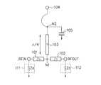
図1は、バイアス回路の構成例を示す回路図である。バイアス回路は、入力ノードRFIN、出力ノードRFOUT、伝送線路101,102、バイアス供給線路103、直流電源電圧ノード104及びシャント容量105を有する。入力ノードRFINの外部には、入力回路のソースインピーダンス111が接続される。ソースインピーダンス111は、インピーダンス値がZ0である。出力ノードRFOUTの外部には、出力回路のロードインピーダンス112が接続される。ロードインピーダンス112は、インピーダンス値がZ0である。インピーダンス値Z0は、例えば50Ωである。(Reference technology)
FIG. 1 is a circuit diagram illustrating a configuration example of a bias circuit. The bias circuit includes an input node RFIN, an output node RFOUT,
入力ノードRFINは、外部からキャリア信号を入力する。出力ノードRFOUTは、外部へキャリア信号を出力する。伝送線路101は、特性インピーダンスZ0を有し、入力ノードRFIN及び第1のノードN1間に接続される。伝送線路102は、特性インピーダンスZ0を有し、第1のノードN1及び出力ノードRFOUT間に接続される。バイアス供給線路103は、第1のノードN1及び第2のノードN2間に接続され、特性インピーダンスYを有し、キャリア信号の周波数に対して1/4波長(λ/4)の線路長を有する。直流電源電圧ノード104は、第2のノードN2に接続され、第2のノードN2に直流電源電圧を供給する。シャント容量105は、第2のノードN2及び基準電位(接地電位)ノード間に接続される。このバイアス回路は、小型であり、低損失な特性を有し、高出力増幅器において内蔵されるバイアス回路に用いることができる。 The input node RFIN inputs a carrier signal from the outside. The output node RFOUT outputs a carrier signal to the outside. The
波長λに相当する周波数を有するキャリア信号は、第1のノードN1で開放として働くので、損失なく伝播される。しかしながら、バイアス回路が大電流を流せるようにするためには、使用している1/4波長のバイアス供給線路103の配線幅を広くする必要があり、1/4波長のバイアス供給線路103の特性インピーダンスYは低化する。これは、バイアス回路の通過帯域を狭くしてしまう。 Since the carrier signal having a frequency corresponding to the wavelength λ acts as an open circuit at the first node N1, it is propagated without loss. However, in order to allow the bias circuit to pass a large current, it is necessary to increase the wiring width of the ¼ wavelength
また、十分な周波数帯域を確保することができれば、複数のキャリア信号に対してバイアス回路を使用することができる。ただし、アプリケーションによっては使用する複数のキャリア信号の周波数以外の周波数において、十分な減衰特性(信号分離特性)が要求されることがある。しかし、このような特性を有するバイアス回路を実現することは困難である。そのため、フィルタ回路と広帯域のバイアス回路を組み合わせることで所望の特性を実現することが考えられる。しかしながら、この方法によると装置全体が大きくなり、小型化の要請にこたえることができない。 If a sufficient frequency band can be secured, a bias circuit can be used for a plurality of carrier signals. However, depending on the application, sufficient attenuation characteristics (signal separation characteristics) may be required at frequencies other than the frequencies of a plurality of carrier signals to be used. However, it is difficult to realize a bias circuit having such characteristics. Therefore, it is conceivable to realize desired characteristics by combining a filter circuit and a wide-band bias circuit. However, according to this method, the entire apparatus becomes large and cannot meet the demand for downsizing.
以下の実施形態では、大電流を流すことができ、かつ、十分広い通過帯域を確保することができるバイアス回路を説明する。また、使用する複数のキャリア信号の周波数以外の周波数において十分な減衰特性を有する小型なマルチキャリア用バイアス回路を説明する。 In the following embodiments, a bias circuit capable of flowing a large current and ensuring a sufficiently wide pass band will be described. A small multi-carrier bias circuit having sufficient attenuation characteristics at frequencies other than the frequencies of a plurality of carrier signals to be used will be described.
(第1の実施形態)
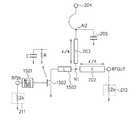
図2は、本発明の第1の実施形態によるバイアス回路の構成例を示す回路図である。バイアス回路は、入力ノードRFIN、出力ノードRFOUT、伝送線路201,202、バイアス供給線路203、直流電源電圧ノード204及びシャント容量205を有する。入力ノードRFINの外部には、入力回路のソースインピーダンス211が接続される。ソースインピーダンス211は、インピーダンス値がZ0である。出力ノードRFOUTの外部には、出力回路のロードインピーダンス212が接続される。ロードインピーダンス212は、インピーダンス値がZ0である。インピーダンス値Z0は、例えば50Ωである。(First embodiment)
FIG. 2 is a circuit diagram showing a configuration example of the bias circuit according to the first embodiment of the present invention. The bias circuit includes an input node RFIN, an output node RFOUT,
入力ノードRFINは、外部からキャリア信号を入力する。出力ノードRFOUTは、外部へキャリア信号を出力する。第1の伝送線路201は、入力ノードRFIN及び第1のノードN1間に接続され、特性インピーダンスXを有し、キャリア信号の周波数に対して1/4波長(λ/4)の線路長を有する。第2の伝送線路202は、第1のノードN1及び出力ノードRFOUT間に接続され、特性インピーダンスXを有し、キャリア信号の周波数に対して1/4波長の線路長を有する。バイアス供給線路203は、第1のノードN1及び第2のノードN2間に接続され、特性インピーダンスYを有し、キャリア信号の周波数に対して1/4波長の線路長を有する。直流電源電圧ノード204は、第2のノードN2に接続され、第2のノードN2に直流電源電圧を供給する。シャント容量205は、第2のノードN2及び基準電位(接地電位)ノード間に接続される。基準電位ノードは、例えば接地導体である。このバイアス回路は、小型であり、低損失な特性を有し、高出力増幅器において内蔵されるバイアス回路に用いることができる。 The input node RFIN inputs a carrier signal from the outside. The output node RFOUT outputs a carrier signal to the outside. The
以上のように、バイアス回路は、直流電源電圧ノード204から1/4波長のバイアス供給線路203を介して分岐し、一方へは1/4波長の伝送線路201を介して入力ノードRFINへ接続され、他方へは1/4波長の伝送線路202を介して出力ノードRFOUTへ接続される。本実施形態では、1/4波長の長さを有するバイアス供給線路203に対して、最適化された特性インピーダンスXを持つ1/4波長の伝送線路201及び202を両側に配置する。 As described above, the bias circuit branches from the DC power
バイアス回路は、キャリア信号の中心周波数よりも高周波数側で容量性であり、低周波数側で誘導性である。高周波数側で誘導性であり、低周波数側で容量性特性を示す低インピーダンスの伝送線路を組み合わせることにより、周波数依存性を相殺することができる。1/4波長の長さを有するバイアス供給線路203に対して、1/4波長の伝送線路201及び202を両側に配置する理由は、キャリア信号の中心周波数における通過特性を悪化させないためである。 The bias circuit is capacitive on the higher frequency side than the center frequency of the carrier signal and is inductive on the lower frequency side. By combining a low impedance transmission line that is inductive on the high frequency side and exhibits capacitive characteristics on the low frequency side, the frequency dependence can be offset. The reason why the quarter
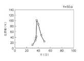
図3は、バイアス供給線路203の特性インピーダンスYが50Ωの場合、伝送線路201及び202の特性インピーダンスXを変化させた場合の比帯域を示すグラフである。比帯域は、入力ノードRFINに信号を入力したときの反射損失が−20dB以下となる帯域の、中心周波数に対する比を示す。特性インピーダンスXに応じて、比帯域も変化する。特性インピーダンスXが37Ωになったとき比帯域は最大値をとり、100%を超える。したがって、特性インピーダンスYが50Ωのとき、特性インピーダンスXの最適値は37Ωであり、比帯域が最大値となり、反射損失が最も少ない。 FIG. 3 is a graph showing a band ratio when the characteristic impedance X of the
図4は、図1のバイアス回路の通過特性411及び反射特性412と、図2のバイアス回路の通過特性401及び反射特性402とを比較した図である。通過特性401及び411は、入力ノードRFINの入力信号の大きさに対する出力ノードRFOUTの出力信号の大きさを示し、大きいほど通過損失が少ないことを示す。反射特性402及び412は、入力ノードRFINに入力した信号の大きさに対する反射信号の大きさを示し、小さいほど反射損失が少ないことを示す。キャリア信号の中心周波数は、例えば9.5GHzである。9.5GHzの中心周波数の低周波数側と高周波数側で、図2のバイアス回路の通過特性401は、図1のバイアス回路の通過特性411に対して向上していることが確認できる。また、図2のバイアス回路の反射特性402についても、図1のバイアス回路の反射特性412に対して向上している。 FIG. 4 is a diagram comparing the
図5は、バイアス供給線路203の特性インピーダンスYを変化させた場合の伝送線路201及び202の特性インピーダンスXの最適値を示すグラフである。特性インピーダンスYの値に対して、特性インピーダンスXの最適値は変化する。特性インピーダンスYが大きくなると、特性インピーダンスXの最適値も大きくなる。図2の入力回路のソースインピーダンス211の値Z0及び出力回路のロードインピーダンス212の値Z0は、50Ωである。図1のバイアス回路では、伝送線路101及び102の特性インピーダンスZ0は、ソースインピーダンス211及びロードインピーダンス212の値Z0と同じである。これに対し、図2のバイアス回路の特性インピーダンスXは、ソースインピーダンス211及びロードインピーダンス212の値Z0より小さい。すなわち、第1の伝送線路201の特性インピーダンスXは、入力ノードRFINに接続される入力回路のソースインピーダンス211の値Z0より小さい。また、第2の伝送線路202の特性インピーダンスXは、出力ノードRFOUTに接続される出力回路のロードインピーダンス212の値Z0より小さい。 FIG. 5 is a graph showing the optimum value of the characteristic impedance X of the
図6は、特性インピーダンスYの値に対して、図5の特性インピーダンスXの値が最適化された場合の比帯域を示すグラフである。特性601は、図2のバイアス回路の比帯域特性を示す。特性602は、図1のバイアス回路の比帯域特性を示す。図2のバイアス回路の比帯域特性601は、図1のバイアス回路の比帯域特性602に対して、大幅な帯域向上が認められる。 FIG. 6 is a graph showing a ratio band when the value of the characteristic impedance X in FIG. 5 is optimized with respect to the value of the characteristic impedance Y. A characteristic 601 indicates a ratio band characteristic of the bias circuit of FIG. A characteristic 602 indicates a ratio band characteristic of the bias circuit of FIG. The
バイアス回路が大電流を流すためには、バイアス供給線路203の配線幅を広くする必要があり、バイアス供給線路203の特性インピーダンスYは低化する。本実施形態のバイアス回路は、バイアス供給線路203の配線幅を広くしてバイアス供給線路203に大電流を流すことができる。その場合、特性インピーダンスYが小さくても、伝送線路201及び202の特性インピーダンスXを最適化することにより、十分広い通過帯域を確保することができる。バイアス供給線路203の配線幅は、所望の電流容量を満足するように定めることができる。 In order for the bias circuit to pass a large current, the wiring width of the
本実施形態のバイアス回路は、異なる複数の周波数のキャリア信号を使用することができる。例えば、5GHz、9.5GHz及び14GHzの3つの異なる周波数のキャリア信号を使用することができる。その場合、使用する複数の周波数以外の周波数において、十分な減衰特性(信号分離特性)が要求される。 The bias circuit of this embodiment can use carrier signals having different frequencies. For example, three different frequency carrier signals of 5 GHz, 9.5 GHz, and 14 GHz can be used. In that case, sufficient attenuation characteristics (signal separation characteristics) are required at frequencies other than a plurality of frequencies to be used.
上記のように、本実施形態のバイアス回路は、バイアス供給線路203に対して、最適化された特性インピーダンスXを持つ伝送線路201及び202を両側に配置する。また、信号分離特性を向上させるためには、バイアス供給線路203の特性インピーダンスYを十分に低くする必要がある。 As described above, the bias circuit of the present embodiment arranges the
図7は、図1のバイアス回路の通過特性711及び反射特性712と、図2のバイアス回路の通過特性701及び反射特性702とを比較した図である。図2のバイアス回路のバイアス供給線路203の特性インピーダンスYは、10Ωである。伝送線路201及び202の特性インピーダンスXは、図9に示す最適値である。図2のバイアス回路の通過特性701は、図1のバイアス回路の通過特性711に対して、使用する5GHz、9.5GHz及び14GHzの3つの周波数で向上していることが確認できる。また、図2のバイアス回路の反射特性702も、図1のバイアス回路の通過特性712に対して、使用する5GHz、9.5GHz及び14GHzの3つの周波数で向上していることが確認できる。 7 is a diagram comparing the
図7は図2のバイアス回路の特性インピーダンスYが10Ωの場合の通過特性701及び反射特性702を示すグラフであり、図8は図2のバイアス回路の特性インピーダンスYが2Ωの場合の通過特性801及び反射特性802を示すグラフである。図8の特性インピーダンスYが2Ωのときの通過特性801及び反射特性802は、図7の特性インピーダンスYが10Ωのときの通過特性701及び反射特性702に対して、使用する5GHz、9.5GHz及び14GHz以外の7GHz近傍及び12GHz近傍における通過損失及び反射損失が増加しており、信号分離特性が向上していることを示している。すなわち、図2のバイアス回路は、不要な7GHz近傍及び12GHz近傍の周波数を除去するフィルタ機能を有するので、別途フィルタを設ける必要がなく、小型化することができる。 7 is a graph showing the
図7及び図8において、本実施形態は、入力ノードRFINに入力する信号の反射特性702及び802が異なる3つの周波数5GHz、9.5GHz及び14GHzにおいて極小値を有する。また、異なる3つの周波数5GHz、9.5GHz及び14GHzにおいて通過特性が最大となるように、伝送線路201及び202の特性インピーダンスXの最適値を設定することができる。また、異なる3つの周波数5GHz、9.5GHz及び14GHzにおいて所望の通過特性が得られるように、バイアス供給線路203の配線幅を設定することができる。 7 and 8, the present embodiment has local minimum values at three frequencies of 5 GHz, 9.5 GHz, and 14 GHz with
図9は、バイアス供給線路203の特性インピーダンスYを変化させた場合の伝送線路201及び202の特性インピーダンスXの最適値を示すグラフである。特性インピーダンスYの値に対して、特性インピーダンスXの最適値は変化する。特性インピーダンスYが大きくなると、特性インピーダンスXの最適値も大きくなる。図2の入力回路のソースインピーダンス211の値Z0及び出力回路のロードインピーダンス212の値Z0は、50Ωである。図1のバイアス回路では、伝送線路101及び102の特性インピーダンスZ0は、ソースインピーダンス211及びロードインピーダンス212の値Z0と同じである。これに対し、図2のバイアス回路の特性インピーダンスXは、ソースインピーダンス211及びロードインピーダンス212の値Z0より小さい。 FIG. 9 is a graph showing the optimum value of the characteristic impedance X of the
図10は、バイアス供給線路203の特性インピーダンスYを変化させた場合の信号分離特性を示すグラフである。伝送線路201及び202の特性インピーダンスXは、図9に示す最適値を用いている。信号分離特性は、不要な周波数7.25GHzにおける反射特性を示し、大きいほど反射損失が大きく、信号分離特性が優れていることを示す。特性インピーダンスYに応じて、信号分離特性は変化する。特性インピーダンスYが小さいほど、信号分離特性が優れ、不要な周波数の信号を通過させず、必要な3つの周波数5GHz、9.5GHz及び14GHzの信号のみを通過させることができる。 FIG. 10 is a graph showing signal separation characteristics when the characteristic impedance Y of the
本実施形態のバイアス回路は、複数の周波数のキャリア信号を使用することができ、使用する複数のキャリア信号の周波数以外の周波数において、十分な減衰特性(信号分離特性)を得ることができる。また、バイアス回路は、不要な周波数の信号を減衰させるフィルタ機能を有するので、別途フィルタを設ける必要がない。本実施形態によれば、使用する複数のキャリア信号の周波数以外の周波数において十分な減衰特性を有する小型なマルチキャリア用バイアス回路を実現することができる。 The bias circuit of this embodiment can use carrier signals having a plurality of frequencies, and can obtain sufficient attenuation characteristics (signal separation characteristics) at frequencies other than the frequencies of the plurality of carrier signals to be used. Further, since the bias circuit has a filter function for attenuating a signal having an unnecessary frequency, it is not necessary to provide a separate filter. According to the present embodiment, it is possible to realize a small multicarrier bias circuit having sufficient attenuation characteristics at frequencies other than the frequencies of a plurality of carrier signals to be used.
なお、伝送線路201は、第1のインピーダンス変換素子であればよい。第1のインピーダンス変換素子201は、入力ノードRFIN及び第1のノードN1間に接続され、キャリア信号の周波数に対して1/4波長のインピーダンス変換を行う。 The
また、伝送線路202は、第2のインピーダンス変換素子であればよい。第2のインピーダンス変換素子202は、第1のノードN1及び出力ノードRFOUT間に接続され、キャリア信号の周波数に対して1/4波長のインピーダンス変換を行う。 The
また、バイアス供給線路203は、第3のインピーダンス変換素子であればよい。第3のインピーダンス変換素子203は、第1のノードN1及び第2のノードN2間に接続され、キャリア信号の周波数に対して1/4波長のインピーダンス変換を行う。 The
また、シャント容量205は、接地回路であればよい。接地回路205は、第2のノードN2を交流接地状態にする。 The
以下の第2〜第12の実施形態では、上記の第1〜第3のインピーダンス変換素子及び接地回路の他の例を示す。 In the following second to twelfth embodiments, other examples of the first to third impedance conversion elements and the ground circuit are shown.
(第2の実施形態)
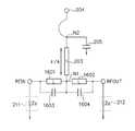
図11は、本発明の第2の実施形態によるバイアス回路の構成例を示す回路図である。図11のバイアス回路は、図2のバイアス回路に対して、線路201〜203の代わりに誘導性素子1101〜1103及び容量性素子1111〜1113を設けたものである。以下、本実施形態が第1の実施形態と異なる点を説明する。第1の誘導性素子1101は、入力ノードRFIN及び第1のノードN1間に接続される。第2の誘導性素子1102は、第1のノードN1及び出力ノードRFOUT間に接続される。第3の誘導性素子1103は、第1のノードN1及び第2のノードN2間に接続される。第1の容量性素子1111は、入力ノードRFIN及び基準電位ノード間に接続される。第2の容量性素子1112は、出力ノードRFOUT及び基準電位ノード間に接続される。第3の容量性素子1113は、第1のノードN1及び基準電位ノード間に接続される。誘導性素子1101〜1103は、伝送線路のインダクタ成分でもよい。(Second Embodiment)
FIG. 11 is a circuit diagram showing a configuration example of a bias circuit according to the second embodiment of the present invention. The bias circuit of FIG. 11 is different from the bias circuit of FIG. 2 in that
第1の誘導性素子1101及び第1の容量性素子1111は、第1の実施形態の第1のインピーダンス変換素子に対応する。第2の誘導性素子1102及び第2の容量性素子1112は、第1の実施形態の第2のインピーダンス変換素子に対応する。第3の誘導性素子1103及び第3の容量性素子1113は、第1の実施形態の第3のインピーダンス変換素子に対応する。 The first
以上のように、誘導性素子1103及び容量性素子1113は共振し、その共振周波数がキャリア信号の周波数に一致するように設計する。キャリア信号の中心周波数をfc、誘導性素子1103のインダクタンス値をL、容量性素子1113のキャパシタンス値をCとすると、fc=1/{2×π×√(L×C)}になるように、インダクタンス値L及びキャパシタンス値Cを決める。 As described above, the
また、誘導性素子1101,1102及び容量性素子1111,1112は共振し、その共振周波数がキャリア信号の周波数fcに一致するように設計する。キャリア信号の中心周波数をfc、誘導性素子1101,1102のインダクタンス値をL、容量性素子1111,1112のキャパシタンス値をCとすると、fc=1/{2×π×√(L×C)}になるように、インダクタンス値L及びキャパシタンス値Cを決める。 Further, the
本実施形態は、第1の実施形態と同様の効果を有する。 The present embodiment has the same effect as the first embodiment.
(第3の実施形態)
図12は、本発明の第3の実施形態によるバイアス回路の構成例を示す回路図である。図12のバイアス回路は、図2のバイアス回路に対して、伝送線路201及び202の代わりに伝送線路1201及び1202を設けたものである。以下、本実施形態が第1の実施形態と異なる点を説明する。(Third embodiment)
FIG. 12 is a circuit diagram showing a configuration example of a bias circuit according to the third embodiment of the present invention. The bias circuit of FIG. 12 is obtained by providing
入力ノードRFINの外部には、入力回路のソースインピーダンス1211が接続される。ソースインピーダンス1211は、インピーダンス値がZ1である。出力ノードRFOUTの外部には、出力回路のロードインピーダンス1212が接続される。ロードインピーダンス1212は、インピーダンス値がZ2である。ソースインピーダンス1211のインピーダンス値Z1とロードインピーダンス1212のインピーダンス値Z2とは相互に異なる。 A
第1の伝送線路1201は、入力ノードRFIN及び第1のノードN1間に接続され、特性インピーダンスX1を有し、キャリア信号の周波数に対して1/4波長の線路長を有する。第2の伝送線路1202は、第1のノードN1及び出力ノードRFOUT間に接続され、特性インピーダンスX2を有し、キャリア信号の周波数に対して1/4波長の線路長を有する。第1の伝送線路1201の特性インピーダンスX1と第2の伝送線路1202の特性インピーダンスX2とは相互に異なる。 The
ソースインピーダンス1211のインピーダンス値Z1とロードインピーダンス1212のインピーダンス値Z2とが相互に異なる場合には、X12/Z1=X22/Z2になるように、特性インピーダンスX1及びX2を決める。When the impedance value Z1 of the
入力ノードRFINに接続される入力回路のソースインピーダンス1211の値Z1が出力ノードRFOUTに接続される出力回路のロードインピーダンス1212の値Z2より大きいときには、第1の伝送線路(第1のインピーダンス変換素子)1201の特性インピーダンスX1は第2の伝送線路(第2のインピーダンス変換素子)1202の特性インピーダンスX2より大きい。 When the value Z1 of the
また、入力ノードRFINに接続される入力回路のソースインピーダンス1211の値Z1が出力ノードRFOUTに接続される出力回路のロードインピーダンス1212の値Z2より小さいときには、第1の伝送線路(第1のインピーダンス変換素子)1201の特性インピーダンスX1は第2の伝送線路(第2のインピーダンス変換素子)1202の特性インピーダンスX2より小さい。 When the value Z1 of the
本実施形態は、第1の実施形態と同様の効果を有する。 The present embodiment has the same effect as the first embodiment.
(第4の実施形態)
図13は、本発明の第4の実施形態によるバイアス回路の構成例を示す回路図である。図13のバイアス回路は、図2のバイアス回路に対して、伝送線路201及び202の代わりに誘導性素子1101,1102及びnチャネル電界効果トランジスタ1301,1302を設けたものである。以下、本実施形態が第1の実施形態と異なる点を説明する。(Fourth embodiment)
FIG. 13 is a circuit diagram showing a configuration example of a bias circuit according to the fourth embodiment of the present invention. The bias circuit of FIG. 13 is different from the bias circuit of FIG. 2 in that
第1の誘導性素子1101は、入力ノードRFIN及び第1のノードN1間に接続される。第2の誘導性素子1102は、第1のノードN1及び出力ノードRFOUT間に接続される。第1のトランジスタ1301は、ドレインが入力ノードRFINに接続され、ゲートが制御ノードCTLに接続され、ソースが基準電位ノードに接続される。第2のトランジスタ1302は、ドレインが出力ノードRFOUTに接続され、ゲートが制御ノードCTLに接続され、ソースが基準電位ノードに接続される。 The first
第1の誘導性素子1101及び第1のトランジスタ1301は、第1の実施形態の第1のインピーダンス変換素子に対応する。第2の誘導性素子1102及び第2のトランジスタ1302は、第1の実施形態の第2のインピーダンス変換素子に対応する。 The first
制御ノードCTLをローレベルにすると、トランジスタ1301及び1302はオフし、図11の容量性素子1111及び1112として機能する。その場合、図11のバイアス回路と同様に、容量性素子としてのトランジスタ1301,1302及び誘導性素子1101,1102は共振し、その共振周波数がキャリア信号の周波数fcに一致するように設計する。キャリア信号の中心周波数をfc、誘導性素子1101,1102のインダクタンス値をL、トランジスタ(容量性素子)1301,1302のキャパシタンス値をCとすると、fc=1/{2×π×√(L×C)}になるように、インダクタンス値L及びキャパシタンス値Cを決める。この共振により、入力ノードRFINに入力されたキャリア信号は、バイアス回路を通過し、出力ノードRFOUTから出力される。 When the control node CTL is set to a low level, the
また、制御ノードCTLをハイレベルにすると、トランジスタ1301及び1302はオンし、抵抗として機能する。その場合、バイアス回路はLC共振せず、入力ノードRFINに入力されたキャリア信号は遮断され、出力ノードRFOUTからはキャリア信号が出力されない。 When the control node CTL is set to a high level, the
以上のように、制御ノードCTLのレベルを制御することにより、バイアス回路は、高周波数スイッチ回路として機能する。制御レベルCTLがローレベルの場合、本実施形態は、第1の実施形態と同様の効果を有する。 As described above, the bias circuit functions as a high-frequency switch circuit by controlling the level of the control node CTL. When the control level CTL is a low level, the present embodiment has the same effect as the first embodiment.
(第5の実施形態)
図14は、本発明の第5の実施形態によるバイアス回路の構成例を示す回路図である。図14のバイアス回路は、図13のバイアス回路に対して、トランジスタ1301,1302の代わりにダイオード1401,1402を設けたものである。以下、本実施形態が第4の実施形態と異なる点を説明する。(Fifth embodiment)
FIG. 14 is a circuit diagram showing a configuration example of a bias circuit according to the fifth embodiment of the present invention. The bias circuit of FIG. 14 is obtained by providing
第1のダイオード1401は、アノードが基準電位ノードに接続され、カソードが入力ノードRFINに接続される。第2のダイオード1402は、アノードが基準電位ノードに接続され、カソードが出力ノードRFOUTに接続される。 The
ダイオード1401及び1402は、逆バイアスが印加されると、容量性素子として機能する。すなわち、ダイオード1401及び1402は、図13のトランジスタ1301及び1302のオフ状態と同じ機能を果たす。本実施形態は、第4の実施形態と同様に、容量性素子としてのダイオード1401,1402及び誘導性素子1101,1102は共振し、その共振周波数がキャリア信号の周波数fcに一致するように、誘導性素子1101,1102のインダクタンス値L及びダイオード1401,1402のキャパシタンス値Cを設計する。すなわち、fc=1/{2×π×√(L×C)}を満たす必要がある。 The
第1の誘導性素子1101及び第1のダイオード1401は、第1の実施形態の第1のインピーダンス変換素子に対応する。第2の誘導性素子1102及び第2のダイオード1402は、第1の実施形態の第2のインピーダンス変換素子に対応する。本実施形態は、第4の実施形態のトランジスタ1301及び1302のオフ状態と同様の効果を有する。 The first
(第6の実施形態)
図15は、本発明の第6の実施形態によるバイアス回路の構成例を示す回路図である。図15のバイアス回路は、図2のバイアス回路に対して、第1の伝送線路201の代わりに整合回路1501、nチャネル電界効果トランジスタ1502及び第1の誘導性素子1503を設けたものである。以下、本実施形態が第1の実施形態と異なる点を説明する。(Sixth embodiment)
FIG. 15 is a circuit diagram showing a configuration example of a bias circuit according to the sixth embodiment of the present invention. The bias circuit of FIG. 15 is different from the bias circuit of FIG. 2 in that a
整合回路1501は、入力ノードRFIN及び第1のトランジスタ1502のゲート間に接続される。第1のトランジスタ1502のソースは、基準電位ノードに接続される。第1の誘導性素子1503は、第1のトランジスタ1502のドレイン及び第1のノードN1間に接続される。なお、第1の誘導性素子1503は、伝送線路のインダクタ成分でもよい。 The
第1のトランジスタ1502の出力回路は、抵抗R及び容量Cの並列接続の等価回路で表わすことができる。この場合、L/(R×C)=X2/Z0となるように、各パラメータを決める。ここで、Lは第1の誘導性素子1503のインダクタンス値、Xは伝送線路202の特性インピーダンス、Z0はソースインピーダンス211及びロードインピーダンス212の値である。The output circuit of the
また、第4の実施形態と同様に、第1のトランジスタ1502の出力容量C及び第1の誘導性素子1502は共振し、その共振周波数がキャリア信号の周波数fcに一致するように、第1の誘導性素子1503のインダクタンス値L及び第1のトランジスタ1502の出力容量Cを設計する。すなわち、fc=1/{2×π×√(L×C)}を満たす必要がある。 Similarly to the fourth embodiment, the output capacitance C of the
バイアス回路内の第1のトランジスタ1502は、入力信号を増幅する高周波数増幅器として機能する。第1のトランジスタ1502及び第1の誘導性素子1503及び整合回路1501は、第1の実施形態の第1のインピーダンス変換素子に対応する。本実施形態は、第1の実施形態と同様の効果を有する。 The
(第7の実施形態)
図16は、本発明の第7の実施形態によるバイアス回路の構成例を示す回路図である。図16のバイアス回路は、図2のバイアス回路に対して、伝送線路201及び202の代わりに誘導性素子1601,1602及び容量性素子1603,1604を設けたものである。以下、本実施形態が第1の実施形態と異なる点を説明する。(Seventh embodiment)
FIG. 16 is a circuit diagram showing a configuration example of a bias circuit according to the seventh embodiment of the present invention. The bias circuit of FIG. 16 is different from the bias circuit of FIG. 2 in that
第1の誘導性素子1601は、入力ノードRFIN及び第1のノードN1間に接続される。第1の容量性素子1603は、第1の誘導性素子1601に並列に接続される。第2の誘導性素子1602は、第1のノードN1及び出力ノードRFOUT間に接続される。第2の容量性素子1604は、第2の誘導性素子1602に並列に接続される。誘導性素子1601及び1602は、伝送線路のインダクタ成分でもよい。 The first
第1の誘導性素子1601及び第1の容量性素子1603は、第1の実施形態の第1のインピーダンス変換素子に対応する。第2の誘導性素子1602及び第2の容量性素子1604は、第1の実施形態の第2のインピーダンス変換素子に対応する。 The first
第4の実施形態と同様に、誘導性素子1601,1602及び容量性素子1603,1604は共振し、その共振周波数がキャリア信号の周波数fcに一致するように、誘導性素子1601,1602のインダクタンス値L及び容量性素子1603,1604のキャパシタンス値Cを設計する。すなわち、fc=1/{2×π×√(L×C)}を満たす必要がある。本実施形態は、第1の実施形態と同様の効果を有する。 As in the fourth embodiment, the
(第8の実施形態)
図17は、本発明の第8の実施形態によるバイアス回路の構成例を示す回路図である。図17のバイアス回路は、図16のバイアス回路に対して、容量性素子1603,1604の代わりにnチャネル電界効果トランジスタ1701,1702を設けたものである。以下、本実施形態が第7の実施形態と異なる点を説明する。(Eighth embodiment)
FIG. 17 is a circuit diagram showing a configuration example of a bias circuit according to the eighth embodiment of the present invention. The bias circuit in FIG. 17 is different from the bias circuit in FIG. 16 in that n-channel
第1のトランジスタ1701は、ゲートが制御ノードCTLに接続され、ドレインが入力ノードRFINに接続され、ソースが第1のノードN1に接続される。第2のトランジスタ1702は、ゲートが制御ノードCTLに接続され、ドレインが第1のノードN1に接続され、ソースが出力ノードRFOUTに接続される。 The
第1の誘導性素子1601及び第1のトランジスタ1701は、第1の実施形態の第1のインピーダンス変換素子に対応する。第2の誘導性素子1602及び第2のトランジスタ1702は、第1の実施形態の第2のインピーダンス変換素子に対応する。 The first
制御ノードCTLをローレベルにすると、トランジスタ1701及び1702はオフし、図16の容量性素子1603及び1604として機能する。その場合、図16のバイアス回路と同様に、容量性素子としてのトランジスタ1701,1702及び誘導性素子1601,1602は共振し、その共振周波数がキャリア信号の周波数fcに一致するように設計する。キャリア信号の中心周波数をfc、誘導性素子1601,1602のインダクタンス値をL、トランジスタ(容量性素子)1701,1702のキャパシタンス値をCとすると、fc=1/{2×π×√(L×C)}になるように、インダクタンス値L及びキャパシタンス値Cを決める。この共振により、入力ノードRFINに入力されたキャリア信号は、バイアス回路を通過し、出力ノードRFOUTから出力される。 When the control node CTL is set to a low level, the
また、制御ノードCTLをハイレベルにすると、トランジスタ1701及び1702はオンし、抵抗として機能する。その場合、バイアス回路はLC共振せず、入力ノードRFINに入力されたキャリア信号は遮断され、出力ノードRFOUTからはキャリア信号が出力されない。 When the control node CTL is set to a high level, the
以上のように、制御ノードCTLのレベルを制御することにより、バイアス回路は、高周波数スイッチ回路として機能する。制御レベルCTLがローレベルの場合、本実施形態は、第7の実施形態と同様の効果を有する。 As described above, the bias circuit functions as a high-frequency switch circuit by controlling the level of the control node CTL. When the control level CTL is a low level, the present embodiment has the same effect as the seventh embodiment.
(第9の実施形態)
図18は、本発明の第9の実施形態によるバイアス回路の構成例を示す回路図である。図18のバイアス回路は、図12のバイアス回路に対して、誘導性素子1801及びnチャネル電界効果トランジスタ1802を追加したものである。以下、本実施形態が第3の実施形態と異なる点を説明する。(Ninth embodiment)
FIG. 18 is a circuit diagram showing a configuration example of a bias circuit according to the ninth embodiment of the present invention. The bias circuit of FIG. 18 is obtained by adding an
伝送線路1202は、第1のノードN1に接続され、キャリア信号の周波数に対して1/4波長の線路長をもつ。誘導性素子1801は、伝送線路1202及びトランジスタ1802のゲート間に接続される。なお、誘導性素子1801は、伝送線路のインダクタ成分でもよい。トランジスタ1802は、ドレインが出力ノードRFOUTに接続され、ソースが基準電位ノードに接続される。伝送線路1202、誘導性素子1801及びトランジスタ1802は、第1の実施形態の第2のインピーダンス変換素子に対応する。 The
第3の実施形態と同様に、ソースインピーダンス1211の値Z1とロードインピーダンス1212の値Z2が異なる場合には、X12/Z1=X22/Z2を満たすように、第1の伝送線路1201の特性インピーダンスX1及び第2の伝送線路1202の特性インピーダンスX2を決める。Similar to the third embodiment, when the value Z1 of the
トランジスタ1802の入力回路は、ゲート容量(入力容量)Cの等価回路で表わすことができる。誘導性素子1801を設けることにより、誘導性素子1801及びゲート容量Cの共振により、ゲート容量Cの虚数部を打ち消し、抵抗成分の実数部のみを残すことができる。キャリア信号の周波数をfcとすると、fc=1/{2×π×√(L×C)}になるように、誘導性素子1801のインダクタンス値L及びゲート容量Cを決める。 An input circuit of the
バイアス回路内のトランジスタ1802は、入力信号を増幅する高周波数増幅器として機能する。本実施形態は、第3の実施形態と同様の効果を有する。 The
(第10の実施形態)
図19は、本発明の第10の実施形態によるバイアス回路の構成例を示す回路図である。図19のバイアス回路は、図2のバイアス回路に対して、シャント容量205の代わりにラディアルスタブ1901を設けたものである。以下、本実施形態が第1の実施形態と異なる点を説明する。(Tenth embodiment)
FIG. 19 is a circuit diagram showing a configuration example of a bias circuit according to the tenth embodiment of the present invention. The bias circuit of FIG. 19 is obtained by providing a
ラディアルスタブ1901は、一端(左端)が第2のノードN2に接続され、他端(右端)が開放状態であり、キャリア信号の周波数に対して1/4波長の長さをもつ扇形の導体である。ラディアルスタブ1901は、第1の実施形態の接地回路に対応する。ラディアルスタブ1901は、1/4波長の長さを有するので、インピーダンス変換を行うことができる。ラディアルスタブ1901の右端が開放状態であるので、ラディアルスタブ1901の左端に接続される第2のノードN2は短絡状態になる。これにより、ラディアルスタブ1901は、図2のシャント容量205と同様の機能を果たすことができる。本実施形態は、第1の実施形態と同様の効果を有する。 The
(第11の実施形態)
図20は、本発明の第11の実施形態によるバイアス回路の構成例を示す回路図である。図20のバイアス回路は、図2のバイアス回路に対して、シャント容量205の代わりに開放スタブ2001を設けたものである。以下、本実施形態が第1の実施形態と異なる点を説明する。(Eleventh embodiment)
FIG. 20 is a circuit diagram showing a configuration example of the bias circuit according to the eleventh embodiment of the present invention. The bias circuit of FIG. 20 is obtained by providing an
開放スタブ2001は、一端(左端)が第2のノードN2に接続され、他端(右端)が開放状態であり、キャリア信号の周波数に対して1/4波長の長さをもつ導体である。開放スタブ2001は、第1の実施形態の接地回路に対応する。開放スタブ2001は、1/4波長の長さを有するので、インピーダンス変換を行うことができる。開放スタブ2001の右端が開放状態であるので、開放スタブ2001の左端に接続される第2のノードN2は短絡状態になる。これにより、開放スタブ2001は、図2のシャント容量205と同様の機能を果たすことができる。本実施形態は、第1の実施形態と同様の効果を有する。 The
(第12の実施形態)
本発明の第12の実施形態は、第1〜第11の実施形態のバイアス回路において、配線素子はアルミナ基板上に形成され、容量性素子は高誘電率基板上に形成される。また、配線素子及び薄膜容量性素子は、SiC、Si、GaN、InP、GaAs又はサファイヤ基板上に形成される。(Twelfth embodiment)
According to a twelfth embodiment of the present invention, in the bias circuit according to the first to eleventh embodiments, the wiring element is formed on an alumina substrate, and the capacitive element is formed on a high dielectric constant substrate. The wiring element and the thin film capacitive element are formed on SiC, Si, GaN, InP, GaAs or a sapphire substrate.
第1〜第12の実施形態のバイアス回路は、大電流を流すことができ、かつ、十分広い通過帯域を確保することができる。また、使用する複数のキャリア信号の周波数以外の周波数において十分な減衰特性を得ることができる。 The bias circuits of the first to twelfth embodiments can pass a large current and can secure a sufficiently wide pass band. In addition, sufficient attenuation characteristics can be obtained at frequencies other than the frequencies of the plurality of carrier signals used.
なお、上記実施形態は、何れも本発明を実施するにあたっての具体化の例を示したものに過ぎず、これらによって本発明の技術的範囲が限定的に解釈されてはならないものである。すなわち、本発明はその技術思想、又はその主要な特徴から逸脱することなく、様々な形で実施することができる。 The above-described embodiments are merely examples of implementation in carrying out the present invention, and the technical scope of the present invention should not be construed in a limited manner. That is, the present invention can be implemented in various forms without departing from the technical idea or the main features thereof.
201 第1の伝送線路(第1のインピーダンス変換素子)
202 第2の伝送線路(第2のインピーダンス変換素子)
203 バイアス供給線路(第3のインピーダンス変換素子)
204 直流電源電圧ノード
205 シャント容量(接地回路)
211 ソースインピーダンス
212 ロードインピーダンス201 first transmission line (first impedance conversion element)
202 2nd transmission line (2nd impedance conversion element)
203 Bias supply line (third impedance conversion element)
204 DC power
211
Claims (5)
Translated fromJapaneseキャリア信号を出力する出力ノードと、
前記入力ノード及び第1のノード間に接続され、キャリア信号の周波数に対して1/4波長のインピーダンス変換を行う第1のインピーダンス変換素子と、
前記第1のノード及び前記出力ノード間に接続され、キャリア信号の周波数に対して1/4波長のインピーダンス変換を行う第2のインピーダンス変換素子と、
前記第1のノード及び第2のノード間に接続され、キャリア信号の周波数に対して1/4波長のインピーダンス変換を行う第3のインピーダンス変換素子と、
前記第2のノードに接続される直流電源電圧ノードと、
前記第2のノードを交流接地状態にする接地回路と
を有することを特徴とするバイアス回路。An input node for inputting a carrier signal;
An output node for outputting a carrier signal;
A first impedance conversion element that is connected between the input node and the first node, and performs impedance conversion of a quarter wavelength with respect to the frequency of the carrier signal;
A second impedance conversion element that is connected between the first node and the output node and performs an impedance conversion of a quarter wavelength with respect to a frequency of a carrier signal;
A third impedance conversion element connected between the first node and the second node and performing impedance conversion of a quarter wavelength with respect to the frequency of the carrier signal;
A DC power supply voltage node connected to the second node;
And a ground circuit for bringing the second node into an AC ground state.
前記第2のインピーダンス変換素子は、前記第1のノード及び前記出力ノード間に接続される第2の誘導性素子と、前記第2の誘導性素子及び基準電位ノード間に接続される第2の容量性素子とを有し、
前記第3のインピーダンス変換素子は、前記第1のノード及び前記第2のノード間に接続される第3の誘導性素子と、前記第3の誘導性素子及び基準電位ノード間に接続される第2の容量性素子とを有することを特徴とする請求項1記載のバイアス回路。The first impedance conversion element includes a first inductive element connected between the input node and the first node, and a first capacitor connected between the first inductive element and a reference potential node. Having a functional element,
The second impedance conversion element includes a second inductive element connected between the first node and the output node, and a second inductive element connected between the second inductive element and a reference potential node. A capacitive element;
The third impedance conversion element includes a third inductive element connected between the first node and the second node, and a third inductive element connected between the third inductive element and a reference potential node. The bias circuit according to claim 1, comprising two capacitive elements.
前記第2のインピーダンス変換素子は、前記第1のノード及び前記出力ノード間に接続される第2の誘導性素子と、前記第2の誘導性素子及び基準電位ノード間に接続される第2のトランジスタとを有することを特徴とする請求項1記載のバイアス回路。The first impedance conversion element includes a first inductive element connected between the input node and the first node, and a first transistor connected between the first inductive element and a reference potential node. And
The second impedance conversion element includes a second inductive element connected between the first node and the output node, and a second inductive element connected between the second inductive element and a reference potential node. The bias circuit according to claim 1, further comprising a transistor.
前記第2のインピーダンス変換素子は、前記第1のノード及び前記出力ノード間に接続される第2の誘導性素子と、前記第2の誘導性素子及び基準電位ノード間に接続される第2のダイオードとを有することを特徴とする請求項1記載のバイアス回路。The first impedance conversion element includes a first inductive element connected between the input node and the first node, and a first diode connected between the first inductive element and a reference potential node. And
The second impedance conversion element includes a second inductive element connected between the first node and the output node, and a second inductive element connected between the second inductive element and a reference potential node. The bias circuit according to claim 1, further comprising a diode.
Priority Applications (1)
| Application Number | Priority Date | Filing Date | Title |
|---|---|---|---|
| JP2009011321AJP5287286B2 (en) | 2009-01-21 | 2009-01-21 | Bias circuit |
Applications Claiming Priority (1)
| Application Number | Priority Date | Filing Date | Title |
|---|---|---|---|
| JP2009011321AJP5287286B2 (en) | 2009-01-21 | 2009-01-21 | Bias circuit |
Publications (2)
| Publication Number | Publication Date |
|---|---|
| JP2010171650A JP2010171650A (en) | 2010-08-05 |
| JP5287286B2true JP5287286B2 (en) | 2013-09-11 |
Family
ID=42703350
Family Applications (1)
| Application Number | Title | Priority Date | Filing Date |
|---|---|---|---|
| JP2009011321AExpired - Fee RelatedJP5287286B2 (en) | 2009-01-21 | 2009-01-21 | Bias circuit |
Country Status (1)
| Country | Link |
|---|---|
| JP (1) | JP5287286B2 (en) |
Families Citing this family (3)
| Publication number | Priority date | Publication date | Assignee | Title |
|---|---|---|---|---|
| JP5547048B2 (en)* | 2010-12-06 | 2014-07-09 | 株式会社東芝 | Power amplifier bias circuit |
| WO2015100739A1 (en) | 2014-01-06 | 2015-07-09 | 华为技术有限公司 | Doherty power amplifier, communication device and system |
| JP2017079386A (en)* | 2015-10-20 | 2017-04-27 | 三菱電機特機システム株式会社 | Bias circuit |
Family Cites Families (19)
| Publication number | Priority date | Publication date | Assignee | Title |
|---|---|---|---|---|
| JP2830319B2 (en)* | 1990-03-08 | 1998-12-02 | ソニー株式会社 | Transmission / reception switching device |
| FI88564C (en)* | 1991-01-14 | 1993-05-25 | Nokia Mobile Phones Ltd | Controllable high frequency damper |
| JP2621692B2 (en)* | 1991-07-05 | 1997-06-18 | 日本電気株式会社 | High frequency bias supply circuit |
| JPH0555803A (en)* | 1991-08-26 | 1993-03-05 | Mitsubishi Electric Corp | Microwave switch |
| JPH06232601A (en)* | 1993-01-29 | 1994-08-19 | Mitsubishi Electric Corp | Microwave switch circuit |
| JPH06244602A (en)* | 1993-02-15 | 1994-09-02 | Mitsubishi Electric Corp | Microwave integrated circuit and package for the same |
| JPH06260801A (en)* | 1993-03-04 | 1994-09-16 | Mitsubishi Electric Corp | High frequency semiconductor device |
| JPH07111426A (en)* | 1993-10-12 | 1995-04-25 | Fujitsu Ltd | Power amplifier |
| JPH07245501A (en)* | 1994-03-04 | 1995-09-19 | Nec Corp | High frequency bias choke circuit |
| US5495217A (en)* | 1994-06-30 | 1996-02-27 | Philips Electronics North America Corporation | Compact hybrid microwave choke |
| JPH08288703A (en)* | 1995-04-17 | 1996-11-01 | Nec Corp | Microwave switch |
| JPH09214201A (en)* | 1996-01-31 | 1997-08-15 | Mitsubishi Electric Corp | High frequency switch, bias circuit and phase shifter |
| JPH10224107A (en)* | 1997-02-07 | 1998-08-21 | Mitsubishi Electric Corp | Microwave integrated circuit |
| JP2003264402A (en)* | 1997-09-04 | 2003-09-19 | Sanyo Electric Co Ltd | Distributed constant circuit |
| JP3209168B2 (en)* | 1997-11-17 | 2001-09-17 | 日本電気株式会社 | Bias circuit for microwave amplifier |
| JP3474750B2 (en)* | 1997-12-26 | 2003-12-08 | 株式会社東芝 | High frequency integrated circuit device and frequency conversion circuit device |
| JP2001007601A (en)* | 1999-06-18 | 2001-01-12 | Teratec:Kk | Power supply circuit |
| JP2004320669A (en)* | 2003-04-21 | 2004-11-11 | Sony Corp | Data communication device, power supply circuit, and signal transmission circuit |
| JP2007208800A (en)* | 2006-02-03 | 2007-08-16 | Toshiba Corp | Single pole double throw switch for high frequency |
- 2009
- 2009-01-21JPJP2009011321Apatent/JP5287286B2/ennot_activeExpired - Fee Related
Also Published As
| Publication number | Publication date |
|---|---|
| JP2010171650A (en) | 2010-08-05 |
Similar Documents
| Publication | Publication Date | Title |
|---|---|---|
| JP6528845B2 (en) | Antenna matching circuit, antenna circuit, front end circuit and communication device | |
| US7385450B2 (en) | Bias circuit | |
| EP2458730A1 (en) | Radiofrequency amplifier | |
| US8368483B2 (en) | Multiband matching circuit and multiband power amplifier | |
| JP2010068261A (en) | Cascode circuit | |
| US9209760B2 (en) | High-frequency, broadband amplifier circuit | |
| CN103051294A (en) | High-frequency signal amplifier | |
| JP5287286B2 (en) | Bias circuit | |
| US9543898B2 (en) | Microwave amplifier device | |
| US11677367B2 (en) | Power amplifier circuit | |
| KR102775313B1 (en) | High frequency amplifier | |
| JP5862653B2 (en) | Switching circuit and high frequency module | |
| Wu et al. | An S-band 3-W load-reconfigurable power amplifier with 50–76% efficiency for VSWR up to 4: 1 | |
| Colantonio et al. | Simultaneous dual-band high efficiency harmonic tuned power amplifier in GaN technology | |
| US7215221B1 (en) | Harmonic termination circuit for medium bandwidth microwave power amplifiers | |
| US11309842B2 (en) | Power amplifier circuit | |
| JP5241599B2 (en) | Harmonic termination circuit | |
| JP6678827B2 (en) | High frequency amplifier | |
| JP4826536B2 (en) | Phase shift circuit | |
| KR101731563B1 (en) | Apparatus for Matching Impedance for Removing Reflection Noise of Motor Driver | |
| JP2015195449A (en) | Multiband high frequency power amplifier | |
| Figur et al. | RF MEMS variable matching networks for multi-band and multi-mode GaN power amplifiers | |
| JP2018142827A (en) | Semiconductor device and electronic equipment | |
| JP2007201596A (en) | Power distribution circuit | |
| JP5921823B2 (en) | Harmonic suppression circuit |
Legal Events
| Date | Code | Title | Description |
|---|---|---|---|
| A621 | Written request for application examination | Free format text:JAPANESE INTERMEDIATE CODE: A621 Effective date:20111006 | |
| A977 | Report on retrieval | Free format text:JAPANESE INTERMEDIATE CODE: A971007 Effective date:20121115 | |
| A131 | Notification of reasons for refusal | Free format text:JAPANESE INTERMEDIATE CODE: A131 Effective date:20121127 | |
| TRDD | Decision of grant or rejection written | ||
| A01 | Written decision to grant a patent or to grant a registration (utility model) | Free format text:JAPANESE INTERMEDIATE CODE: A01 Effective date:20130507 | |
| A61 | First payment of annual fees (during grant procedure) | Free format text:JAPANESE INTERMEDIATE CODE: A61 Effective date:20130520 | |
| R150 | Certificate of patent or registration of utility model | Ref document number:5287286 Country of ref document:JP Free format text:JAPANESE INTERMEDIATE CODE: R150 | |
| LAPS | Cancellation because of no payment of annual fees |