JP5287045B2 - Liquid crystal display - Google Patents
Liquid crystal displayDownload PDFInfo
- Publication number
- JP5287045B2 JP5287045B2JP2008221459AJP2008221459AJP5287045B2JP 5287045 B2JP5287045 B2JP 5287045B2JP 2008221459 AJP2008221459 AJP 2008221459AJP 2008221459 AJP2008221459 AJP 2008221459AJP 5287045 B2JP5287045 B2JP 5287045B2
- Authority
- JP
- Japan
- Prior art keywords
- liquid crystal
- guide plate
- light guide
- main body
- crystal cell
- Prior art date
- Legal status (The legal status is an assumption and is not a legal conclusion. Google has not performed a legal analysis and makes no representation as to the accuracy of the status listed.)
- Active
Links
- 239000004973liquid crystal related substanceSubstances0.000titleclaimsdescription63
- 210000002858crystal cellAnatomy0.000claimsdescription42
- 230000002093peripheral effectEffects0.000claimsdescription12
- 239000000463materialSubstances0.000claimsdescription7
- 230000003760hair shineEffects0.000claims1
- 230000002265preventionEffects0.000claims1
- 238000009792diffusion processMethods0.000description9
- 210000000078clawAnatomy0.000description3
- 230000004308accommodationEffects0.000description2
- 238000003780insertionMethods0.000description2
- 230000037431insertionEffects0.000description2
- 238000000034methodMethods0.000description2
- 230000001105regulatory effectEffects0.000description2
- 230000003449preventive effectEffects0.000description1
- 239000000758substrateSubstances0.000description1
Images

Landscapes
- Liquid Crystal (AREA)
- Planar Illumination Modules (AREA)
Description
Translated fromJapanese本発明は、各種電子機器に備え付けられるエッジライト方式を採用した液晶表示装置に関するものである。 The present invention relates to a liquid crystal display device employing an edge light system provided in various electronic devices.
エッジライト方式を採用した液晶表示装置においては、LEDから発光された光を導光板の外周面の一部から導光板内に導入し導光板で拡散させた上で液晶セルの背後から照らすようにしている。この場合、導光板に導入された光が導光板の他の外周面から漏洩しないように、導光板の外周面を遮蔽する遮蔽部材が備えられ、この遮蔽部材に液晶セルや導光板等を保持するようにしてユニット化している。 In a liquid crystal display device employing an edge light system, light emitted from an LED is introduced into the light guide plate from a part of the outer peripheral surface of the light guide plate, diffused by the light guide plate, and then illuminated from behind the liquid crystal cell. ing. In this case, a shielding member that shields the outer peripheral surface of the light guide plate is provided so that light introduced into the light guide plate does not leak from the other outer peripheral surface of the light guide plate, and a liquid crystal cell, a light guide plate, or the like is held by this shielding member As a unit.
従来の液晶表示装置としては、液晶セルと、この液晶セルの背後から照明するためのLEDが実装されたプリント基板と、LEDから発光された光を液晶セルに導光するための導光板と、この導光板の外周および背面を覆い光の漏洩を規制する保持部材とを備え、この保持部材に液晶セル、導光板およびプリント基板を保持してユニット化したものがある(例えば、特許文献1参照)。
上述した従来の液晶表示装置においては、液晶セルを一旦導光板やプリント基板とともに保持部材によってユニット化してから、液晶表示装置の筺体に組み込むようにしている。このため、液晶セルや導光板等の部品を保持するための保持部材が必要になることにより部品点数が増加するだけではなく、ユニット化したことによって装置全体が大型化するといった問題があった。 In the above-described conventional liquid crystal display device, the liquid crystal cell is once unitized by a holding member together with the light guide plate and the printed board, and then incorporated into the housing of the liquid crystal display device. For this reason, there is a problem that not only the number of parts is increased due to the necessity of holding members for holding parts such as a liquid crystal cell and a light guide plate, but the whole apparatus is enlarged due to unitization.
本発明は上記した従来の問題に鑑みなされたものであり、その目的とするところは、部品点数を削減し、装置の小型化を図った液晶表示装置を提供するところにある。 The present invention has been made in view of the above-described conventional problems, and an object of the present invention is to provide a liquid crystal display device in which the number of components is reduced and the size of the device is reduced.
この目的を達成するために、本発明は、液晶セルと、この液晶セルの背後から光を照らすバックライトと、このバックライトから発光される光を前記液晶セルの背後に導光する導光板とを備えた液晶表示装置において、前記液晶セルが臨む表示窓が設けられた第1の本体ケースと、この第1の本体ケースとともに装置本体の筺体を形成する第2の本体ケースとを備え、前記第1の本体ケースに、前記導光板の外周面が対向する第1の対向壁を一体に設け、この第1の対向壁の内面を反射面によって形成し、前記第1の対向壁に、前記液晶セルに電気的に接続されたフレキシブルプリント基板を前記筺体外に導出するための切欠きを設け、前記導光板の外周面の一部である切欠きと対向する前記第2の本体ケースの部分に前記第1の対向壁の切欠きに対応した第2の対向壁を一体に設け、この第2の対向壁の内面を反射面によって形成したものである。In order to achieve this object, the present invention provides a liquid crystal cell, a backlight that illuminates light from behind the liquid crystal cell, and a light guide plate that guides light emitted from the backlight to the back of the liquid crystal cell. A first main body case provided with a display window facing the liquid crystal cell, and a second main body case that forms a housing of the apparatus main body together with the first main body case, The first main body case is integrally provided with a first counter wall facing the outer peripheral surface of the light guide plate, and an inner surface of the first counter wall is formed bya reflective surface, andthe first counter wall has the A portion of the second main body case that is provided with a notch for leading out the flexible printed circuit board electrically connected to the liquid crystal cell to the outside of the housing and faces the notch that is a part of the outer peripheral surface of the light guide plate Cutting the first opposing wall Providing the second opposed walls corresponding to come together, inwhich the inner surface of the second opposing wall is formed by the reflecting surface.
本発明は、前記発明のいずれか一つの発明において、前記第1および第2の本体ケースを反射材によって形成したものである。 According to the present invention, in any one of the above inventions, the first and second main body cases are formed of a reflective material.
本発明は、前記発明のいずれか一つの発明において、前記第1の本体ケースに、前記バックライトが実装されるプリント基板を着脱自在に取り付ける弾性係合片を設け、前記液晶セルと前記導光板とを積層した状態で前記第1の対向壁内に収納し、前記第1の本体ケースに取り付けられた前記プリント基板と第1の本体ケースとによって、前記液晶セルと前記導光板とを挟持したものである。 The present invention provides the liquid crystal cell and the light guide plate according to any one of the inventions, wherein the first main body case is provided with an elastic engagement piece for detachably attaching a printed circuit board on which the backlight is mounted. The liquid crystal cell and the light guide plate are sandwiched between the printed board and the first body case attached to the first body case. Is.
本発明は、前記発明のいずれか一つの発明において、前記プリント基板の前記導光板に対向する部位に反射面を設けたものである。 In the invention according to any one of the inventions described above, a reflective surface is provided on a portion of the printed board facing the light guide plate.
本発明は、前記発明のいずれか一つの発明において、前記導光板の表裏の組み間違いを規制する規制手段を備えたものである。 According to the present invention, in any one of the inventions described above, there is provided a regulating means for regulating an assembly error between the front and back of the light guide plate.
本発明によれば、導光板に導入された光の漏洩を規制する第1の対向壁を第1の本体ケースに直接設けたことにより、光の漏洩を規制するための専用の部材を設ける必要がなくなるため、部品点数が削減され、かつ装置の小型化を図ることもできる。また本発明によれば、液晶セルに電気的に接続されたフレキシブル基板を筐体外に導出することができるとともに第1の対向壁および第2の対向壁に反射処理を施す必要がなくなる。According to the present invention, it is necessary to provide a dedicated member for restricting light leakage by directly providing the first main body case with the first opposing wall for restricting light leakage introduced into the light guide plate. Therefore, the number of parts can be reduced and the apparatus can be downsized.In addition, according to the present invention, the flexible substrate electrically connected to the liquid crystal cell can be led out of the casing, and it is not necessary to perform a reflection process onthe first opposing wall and the second opposing wall.
前記発明のうちの一つの発明によれば、第1の対向壁が液晶セルと導光板の組付けの際の案内部材となるので組付けが容易になる。また、第1の対向壁が導光板からの光の漏洩を規制する機能と導光板等の部品の収納機能を兼ねているため、筺体の構造を簡素化することができる。 According to one of the above inventions, the first opposing wall serves as a guide member when the liquid crystal cell and the light guide plate are assembled, so that the assembly is facilitated. Moreover, since the 1st opposing wall serves as the function which controls the leakage of the light from a light-guide plate, and the accommodation function of components, such as a light-guide plate, the structure of a housing can be simplified.
前記発明のうちの一つの発明によれば、導光板の表裏の組み付け間違いを防止することができる。 According to one of the inventions, it is possible to prevent an assembly error between the front and back of the light guide plate.
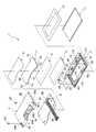
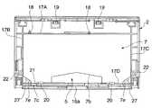
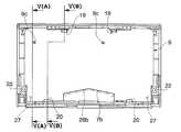
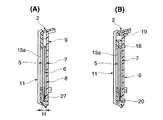
以下、本発明の実施の形態を図に基づいて説明する。図1は本発明に係る液晶表示装置を分解して示す斜視図、図2は同じくアッパーケースの底面図、図3は導光板まで組み付けた状態を示すアッパーケースの底面図、図4は同じくプリント基板までを実装した状態を示すアッパーケースの底面図、図5(A)は図4におけるV(A)-V(A) 線断面図、同図(B)は図4におけるV(B)-V(B) 線断面図である。 Hereinafter, embodiments of the present invention will be described with reference to the drawings. 1 is an exploded perspective view of a liquid crystal display device according to the present invention, FIG. 2 is a bottom view of the upper case, FIG. 3 is a bottom view of the upper case showing a state where the light guide plate is assembled, and FIG. FIG. 5 (A) is a cross-sectional view taken along line V (A) -V (A) in FIG. 4, and FIG. 5 (B) is a cross-sectional view of V (B) − in FIG. It is a V (B) line sectional view.
図1に全体を符号1で示す液晶表示装置は、第1の本体ケースとしてのアッパーケース2と、このアッパーケース2とともに装置本体の筺体を形成する第2の本体ケースとしてのロアーケース3とを備えている。これらアッパーケース2とロアーケース3との間には、液晶セル5、拡散シート6、導光板7、反射シート8、プリント基板9が収納され、アッパーケース2の前面部15の表面には、表示シート10を挟むように透明パネル11が着脱自在に取り付けられる。 1 includes an
アッパーケース2は、図1および図2に示すように表示窓15aを有する前面部15と、この前面部15の周端から一体に立設された囲い壁16とからなり、全体が光を反射する反射材である白色のプラスチックによって一面が開口した浅底の箱状に形成されている。囲い壁16の一部には、液晶セル5の後述するフレキシブルプリント基板25を筺体の外部に導出する切欠き16aが設けられている。 As shown in FIGS. 1 and 2, the
表示窓15aの周囲には、上壁17A、両側壁17B,17C、底壁17Dからなる平面視が枠状に形成された第1の対向壁17が前面部15の裏面から一体に立設されており、底壁17Dには、上記した切欠き16aに対応して切欠き17aが設けられている。この第1の対向壁17の突出高さHは、図5(A)に示すように、この第1の対向壁17内に収納される液晶セル5、拡散シート6、導光板7、反射シート8の厚みの合計と略同じ寸法に形成されている。 Around the
18,18はプリント基板9を位置決めするために、上壁17Aに一体に立設された一対の位置決め用突起である。前面部15の裏面の上部には、先端に爪を有する一対の弾性係合片19,19が一体に立設されており、これら弾性係合片19,19と対向するように、前面部15の裏面の下部には、断面が逆L字状に形成された一対の係合部20,20が一体に立設されている。21は底壁17Dの一方の端部に形成された係入凹部であって、導光板7の後述する一方の突起7cが係入する。22,22は前面部15の裏面の両側部に一体に立設されたスタッドであって、ロアーケース3をアッパーケース2に取り付けるためのねじ23,23が螺合される。
液晶セル5は第1の対向壁17内に嵌合する大きさの扁平な長方形に形成されており、下端中央部から液晶セル5に電気的に接続されたフレキシブルプリント基板25が導出されている。 The
拡散シート6は乳白色の半透明材によって液晶セル5と同じ大きさの長方形に形成されており、後述するように導光板7から導出された光を面方向に拡散させて液晶セル5の背後に導く。 The
導光板7は第1の対向壁17内に嵌合するように扁平な略長方形に形成されており、一面7aに全反射処理が施され、下部に五角形に形成された切欠き7bが設けられている。この切欠き7bの両端部には、突起7c,7dが面方向に突設されており、一方の突起7cの突出長さが他方の突起7dの突出長さよりも長く形成されている。また、導光板7の下端の両端部には、後述するLED27,27から発光された光を導光板7内に導入するために、傾斜するように形成された導光部7e,7eが設けられている。 The
反射シート8は、導光板7と略同じ大きさの略長方形に形成されており、下部には五角形に形成された切欠き8aが設けられている。 The
プリント基板9は液晶セル5の外形よりも大きい略長方形に形成されており、下端部には切欠き8aと同じ大きさの切欠き9aが設けられ、上端には、上記した弾性係合片19,19の爪が係合する凹部9b,9bが設けられている。9c,9cは、プリント基板9をアッパーケース2の所定の位置に組み込むために、アッパーケース2の位置決め突起18,18が係入される位置決め孔である。このプリント基板9の裏面の下部両側には、図3に示すようにバックライトとして機能する一対のLED27,27が実装されている。また、後述するようにプリント基板9がアッパーケース2に取り付けられた状態で、プリント基板9の裏面の導光板7の表面に対向する部位には、反射用塗装を施した反射面(図示せず)が設けられている。 The printed
ロアーケース3は、図1に示すように底部28と、この底部28の周端から一体に立設された囲い壁29とからなり、全体が光を反射する反射材である白色のプラスチックによって一面が開口した浅底の箱状に形成されている。底部28には、ねじ23,23を挿通させるための挿通孔28a,28aが設けられており、底部28の内面には、図4に示すように導光板7の切欠き7bに対向する第2の対向壁28bが一体に立設されている。囲い壁29の一部には、液晶セル5のフレキシブルプリント基板25を筺体の外部に導出する切欠き29aが設けられている。As shown in FIG. 1, the lower case 3 includes a
次に、このように構成された液晶表示装置の組立方法について説明する。図1において、予め、アッパーケース2の前面部15の表面に、表示シート10を挟むように透明パネル11を取り付けておく。この状態で、アッパーケース2の前面部15の裏面側を上方に向け、液晶セル5をアッパーケース2の第1の対向壁17内に収納し、フレキシブルプリント基板25を第1の対向壁17の切欠き17aおよびアッパーケース2の切欠き16aから筺体の外部に導出する。 Next, a method for assembling the liquid crystal display device configured as described above will be described. In FIG. 1, a
次いで、拡散シート6を液晶セル5上に積層するようにして第1の対向壁17内に収納する。さらに、導光板7を拡散シート6上に積層するようにして第1の対向壁17内に収納する。このとき、導光板7の全反射処理が施された一面7aが下方を指向した状態で組み付けられた場合は、一方の突起7cが第1の対向壁17の底壁17Dに乗り上げるため、組み付けることができない。 Next, the
一方、全反射処理が施された一面7aが上方を指向した状態で組み付けた場合は、図3に示すように一方の突起7cが第1の対向壁17の底壁17Dの係合凹部21に係入するため、導光板7をアッパーケース2に組み付けることが可能になる。このように、導光板7の全反射処理が施された一面7aの指向方向を間違えて組み付けるようなことがない。この導光板7の突起7cと、この突起7cの係入を許容する係合凹部21と、突起7cが乗り上がる底壁17Dとが、導光板7の表裏の組み間違いを防止する防止手段を構成している。 On the other hand, when assembled with the one
次いで、反射シート8を導光板7上に積層するようにして第1の対向壁17内に収納する。この状態で、上述したように反射シート8の表面が、第1の対向壁17の突出した先端と略同じ高さ位置に位置する。次いで、プリント基板9によって反射シート8上を覆うように、プリント基板9の位置決め孔9c,9cにアッパーケース2の位置決め突起18,18を係入する。さらに、下端部をアッパーケース2の係合部20,20に係合させ、凹部9b,9bをアッパーケース2の弾性係合片19,19の爪に係合させることにより、プリント基板9をアッパーケース2の第1の対向壁17上に取り付ける。 Next, the
この状態で、第1の対向壁17内に収納された液晶セル5、拡散シート6、導光板7、反射シート8がプリント基板9とアッパーケース2の前面部15とに挟持される。また、プリント基板9に実装されているLED27,27が図3に示すように導光板7の導光部7e,7eに対向し、プリント基板9の裏面に設けた反射面(図示せず)が導光板7の表面に対向する。 In this state, the
次いで、ロアーケース3をアッパーケース2に対向させ、ロアーケース3の挿通孔28aに挿通させたねじ23をアッパーケース2のスタッド22に螺合させることにより、アッパーケース2とロアーケース3とが接合されて液晶表示装置1の筺体が形成される。 Next, the lower case 3 is opposed to the
このように形成された液晶表示装置1においては、LED27から発光された光は、導光板7の導光部7eから導光板7内に導入され、拡散シート6によって拡散されて、液晶セル5を背後から照らす。このとき、導光体7の外周面がアッパーケース2の第1の対向壁17およびロアーケース3の第2の対向壁28bによって囲まれるようにして対向し、これら両ケース2,3が反射材によって形成されているため、導光体7内に導入された光は外周面から漏洩することなく液晶セル5を照らす。このように、導光板7に導入された光の漏洩を規制する第1および第2の対向壁17,28bを両ケース2,3に直接設けたことにより、光の漏洩を規制するための専用の部材を設ける必要がないため、部品点数が削減され、かつ液晶表示装置1の小型化を図ることもできる。 In the thus formed liquid crystal display device 1, the light emitted from the
また、プリント基板9の裏面に設けた反射面(図示せず)が導光板7の表面に対向するため、導光板7に導入された光が導光板7の背面から漏洩することなく、液晶セル5を効率よく照らすことができる。 In addition, since the reflection surface (not shown) provided on the back surface of the printed
また、アッパーケース2の第1の対向壁17が液晶セル5、拡散シート6、導光板7、反射シート8の組付けの際の案内部材となるので組付けが容易になる。また、第1の対向壁17が導光板からの光の漏洩を規制する機能と、導光板7等の収納機能を兼ねているため、筺体の構造を簡素化することができる。 Further, since the first opposing
なお、本実施の形態においては、アッパーケース2の底壁17Dに、液晶セル5のフレキシブルプリント基板25を導出するための切欠き17aを設けたが、フレキシブルプリント基板25を底壁17Dを乗り越えるようにして導出する構造とすれば、切欠き17aを設ける必要はなく、ロアーケース3にも第2の対向壁28bを設けることはない。また、アッパーケース2およびロアーケース3を反射材によって形成したが、導光板7の外周面に対向する第1および第2の対向壁17,28bの内面に反射処理を施すようにすれば、両ケース2,3は必ずしも反射材によって形成することはない。 In the present embodiment, the
1…液晶表示装置、2…アッパーケース(第1の本体ケース)、3…ロアーケース(第2の本体ケース)、5…液晶セル、6…拡散シート、7…導光板、7c…突起、7e…導光部、8…反射シート、9…プリント基板、15…前面部、17…第1の対向壁、19…弾性係合片、21…係合凹部、27…LED(バックライト)、28b…第2の対向壁。 DESCRIPTION OF SYMBOLS 1 ... Liquid crystal display device, 2 ... Upper case (1st main body case), 3 ... Lower case (2nd main body case), 5 ... Liquid crystal cell, 6 ... Diffusion sheet, 7 ... Light guide plate, 7c ... Projection, 7e DESCRIPTION OF SYMBOLS ... Light guide part, 8 ... Reflective sheet, 9 ... Printed circuit board, 15 ... Front part, 17 ... 1st opposing wall, 19 ... Elastic engagement piece, 21 ... Engagement recessed part, 27 ... LED (backlight), 28b ... second opposing wall.
Claims (5)
Translated fromJapaneseら発光される光を前記液晶セルの背後に導光する導光板とを備えた液晶表示装置において
、
前記液晶セルが臨む表示窓が設けられた第1の本体ケースと、この第1の本体ケースと
ともに装置本体の筺体を形成する第2の本体ケースとを備え、
前記第1の本体ケースに、前記導光板の外周面が対向する第1の対向壁を一体に設け、
この第1の対向壁の内面を反射面によって形成し、
前記第1の対向壁に、前記液晶セルに電気的に接続されたフレキシブルプリント基板を前記筺体外に導出するための切欠きを設け、前記導光板の外周面の一部である切欠きと対向する前記第2の本体ケースの部分に前記第1の対向壁の切欠きに対応した第2の対向壁を一体に設け、この第2の対向壁の内面を反射面によって形成したことを特徴とする液晶表示装置。In a liquid crystal display device comprising a liquid crystal cell, a backlight that shines light from behind the liquid crystal cell, and a light guide plate that guides light emitted from the backlight to the back of the liquid crystal cell.
A first main body case provided with a display window facing the liquid crystal cell; and a second main body case that forms a housing of the apparatus main body together with the first main body case;
The first main body case is integrally provided with a first opposing wall facing the outer peripheral surface of the light guide plate,
The inner surface of the first opposing wall is formed bya reflective surface;
The first opposing wall is provided with a notch for leading out the flexible printed circuit board electrically connected to the liquid crystal cell to the outside of the housing, and is opposed to the notch that is a part of the outer peripheral surface of the light guide plate. The second opposing wall corresponding to the notch of the first opposing wall is integrally provided in the second main body case portion, and the inner surface of the second opposing wall is formed by areflective surface. A liquid crystal display device.
前記液晶セルと前記導光板とを積層した状態で前記第1の対向壁内に収納し、前記第1の本体ケースに取り付けられた前記プリント基板と第1の本体ケースとによって、前記液晶セルと前記導光板とを挟持したことを特徴とする請求項1または2記載の液晶表示装置。The first main body case is provided with an elastic engagement piece for detachably attaching a printed board on which the backlight is mounted,
The liquid crystal cell and the light guide plate are stored in the first opposing wall in a stacked state, and the liquid crystal cell is formed by the printed circuit board and the first main body case attached to the first main body case. the liquid crystal display device according to claim 1or 2, wherein the nipping a light guide plate.
Priority Applications (1)
| Application Number | Priority Date | Filing Date | Title |
|---|---|---|---|
| JP2008221459AJP5287045B2 (en) | 2008-08-29 | 2008-08-29 | Liquid crystal display |
Applications Claiming Priority (1)
| Application Number | Priority Date | Filing Date | Title |
|---|---|---|---|
| JP2008221459AJP5287045B2 (en) | 2008-08-29 | 2008-08-29 | Liquid crystal display |
Publications (2)
| Publication Number | Publication Date |
|---|---|
| JP2010054936A JP2010054936A (en) | 2010-03-11 |
| JP5287045B2true JP5287045B2 (en) | 2013-09-11 |
Family
ID=42070912
Family Applications (1)
| Application Number | Title | Priority Date | Filing Date |
|---|---|---|---|
| JP2008221459AActiveJP5287045B2 (en) | 2008-08-29 | 2008-08-29 | Liquid crystal display |
Country Status (1)
| Country | Link |
|---|---|
| JP (1) | JP5287045B2 (en) |
Families Citing this family (1)
| Publication number | Priority date | Publication date | Assignee | Title |
|---|---|---|---|---|
| KR20140018607A (en)* | 2012-08-02 | 2014-02-13 | 삼성디스플레이 주식회사 | Display having a separate light source |
Family Cites Families (5)
| Publication number | Priority date | Publication date | Assignee | Title |
|---|---|---|---|---|
| JP3261928B2 (en)* | 1995-05-22 | 2002-03-04 | 松下電器産業株式会社 | Liquid crystal unit floodlight |
| JP4221076B2 (en)* | 1998-05-25 | 2009-02-12 | 三菱電機株式会社 | Liquid crystal display |
| JP2002006142A (en)* | 2000-06-20 | 2002-01-09 | Enplas Corp | Light guide plate, surface light source device and image display device |
| JP3891843B2 (en)* | 2002-01-08 | 2007-03-14 | 株式会社日立製作所 | Liquid crystal display |
| KR101348247B1 (en)* | 2007-06-07 | 2014-01-09 | 삼성디스플레이 주식회사 | Liquid crystal display device |
- 2008
- 2008-08-29JPJP2008221459Apatent/JP5287045B2/enactiveActive
Also Published As
| Publication number | Publication date |
|---|---|
| JP2010054936A (en) | 2010-03-11 |
Similar Documents
| Publication | Publication Date | Title |
|---|---|---|
| WO2010026810A1 (en) | Illuminating device and liquid crystal display device provided with the same | |
| JP4639714B2 (en) | Liquid crystal display device and portable information terminal equipped with the liquid crystal display device | |
| RU2444067C1 (en) | Electronic package, display device and electronic device | |
| JP3129206U7 (en) | ||
| JP4349557B2 (en) | Liquid crystal display | |
| US7125155B2 (en) | Lighting device, and liquid crystal display device using the same | |
| JP5287045B2 (en) | Liquid crystal display | |
| TWI587038B (en) | Liquid crystal display device | |
| US9535286B2 (en) | Image display device | |
| JP4325918B2 (en) | Liquid crystal display | |
| JP4209410B2 (en) | Light source mounting structure of edge light type backlight module and flat panel display having the light source mounting structure | |
| JP2007272126A (en) | Backlight device for liquid crystal display device | |
| JP2008251220A (en) | Backlight unit and display device | |
| JP4341287B2 (en) | Backlight unit | |
| JP7143153B2 (en) | DISPLAY AND HEAD-UP DISPLAY DEVICE INCLUDING DISPLAY | |
| CN115516590A (en) | Display device | |
| JP2018049810A (en) | Display device and television receiver | |
| JP6750235B2 (en) | Display device, electronic device, and light guide unit | |
| WO2005093503A1 (en) | Liquid crystal display device | |
| JP2007149587A (en) | Backlight device | |
| JP2008203487A (en) | Illuminated electronics | |
| JP6667225B2 (en) | Planar lighting device | |
| JP2025040710A (en) | Display device | |
| JP2007035481A (en) | Plane light source device | |
| JP4481866B2 (en) | Surface light source device |
Legal Events
| Date | Code | Title | Description |
|---|---|---|---|
| A621 | Written request for application examination | Free format text:JAPANESE INTERMEDIATE CODE: A621 Effective date:20110802 | |
| A977 | Report on retrieval | Free format text:JAPANESE INTERMEDIATE CODE: A971007 Effective date:20121121 | |
| A131 | Notification of reasons for refusal | Free format text:JAPANESE INTERMEDIATE CODE: A131 Effective date:20121204 | |
| A521 | Request for written amendment filed | Free format text:JAPANESE INTERMEDIATE CODE: A523 Effective date:20130118 | |
| TRDD | Decision of grant or rejection written | ||
| A01 | Written decision to grant a patent or to grant a registration (utility model) | Free format text:JAPANESE INTERMEDIATE CODE: A01 Effective date:20130507 | |
| A61 | First payment of annual fees (during grant procedure) | Free format text:JAPANESE INTERMEDIATE CODE: A61 Effective date:20130520 | |
| R150 | Certificate of patent or registration of utility model | Ref document number:5287045 Country of ref document:JP Free format text:JAPANESE INTERMEDIATE CODE: R150 | |
| S111 | Request for change of ownership or part of ownership | Free format text:JAPANESE INTERMEDIATE CODE: R313111 | |
| R350 | Written notification of registration of transfer | Free format text:JAPANESE INTERMEDIATE CODE: R350 |