JP5277066B2 - Semiconductor light emitting device and manufacturing method thereof - Google Patents
Semiconductor light emitting device and manufacturing method thereofDownload PDFInfo
- Publication number
- JP5277066B2 JP5277066B2JP2009106875AJP2009106875AJP5277066B2JP 5277066 B2JP5277066 B2JP 5277066B2JP 2009106875 AJP2009106875 AJP 2009106875AJP 2009106875 AJP2009106875 AJP 2009106875AJP 5277066 B2JP5277066 B2JP 5277066B2
- Authority
- JP
- Japan
- Prior art keywords
- layer
- substrate
- electrode
- electrode layer
- insulating layer
- Prior art date
- Legal status (The legal status is an assumption and is not a legal conclusion. Google has not performed a legal analysis and makes no representation as to the accuracy of the status listed.)
- Expired - Fee Related
Links
- 239000004065semiconductorSubstances0.000titleclaimsabstractdescription71
- 238000004519manufacturing processMethods0.000titleclaimsabstractdescription35
- 239000000758substrateSubstances0.000claimsabstractdescription132
- 238000000034methodMethods0.000claimsdescription37
- 238000005253claddingMethods0.000claimsdescription27
- 238000005476solderingMethods0.000claimsdescription2
- 238000000605extractionMethods0.000abstractdescription11
- XUIMIQQOPSSXEZ-UHFFFAOYSA-NSiliconChemical compound[Si]XUIMIQQOPSSXEZ-UHFFFAOYSA-N0.000description26
- 229910052710siliconInorganic materials0.000description26
- 239000010703siliconSubstances0.000description26
- 240000004050Pentaglottis sempervirensSpecies0.000description16
- 235000004522Pentaglottis sempervirensNutrition0.000description16
- 239000010408filmSubstances0.000description14
- 230000004048modificationEffects0.000description14
- 238000012986modificationMethods0.000description14
- 238000010586diagramMethods0.000description9
- 229910001218Gallium arsenideInorganic materials0.000description7
- 238000004544sputter depositionMethods0.000description6
- 229910004298SiO 2Inorganic materials0.000description5
- 229910017083AlNInorganic materials0.000description4
- 238000003776cleavage reactionMethods0.000description4
- 239000000463materialSubstances0.000description4
- 229910052751metalInorganic materials0.000description4
- 239000002184metalSubstances0.000description4
- 238000004806packaging method and processMethods0.000description4
- 230000007017scissionEffects0.000description4
- 230000015572biosynthetic processEffects0.000description3
- 229910000679solderInorganic materials0.000description3
- 238000001771vacuum depositionMethods0.000description3
- 229910018072Al 2 O 3Inorganic materials0.000description2
- 229910017109AlONInorganic materials0.000description2
- 229910052581Si3N4Inorganic materials0.000description2
- 229910004541SiNInorganic materials0.000description2
- 229910010413TiO 2Inorganic materials0.000description2
- QVGXLLKOCUKJST-UHFFFAOYSA-Natomic oxygenChemical compound[O]QVGXLLKOCUKJST-UHFFFAOYSA-N0.000description2
- 238000005516engineering processMethods0.000description2
- 238000009413insulationMethods0.000description2
- 238000010030laminatingMethods0.000description2
- 229910052760oxygenInorganic materials0.000description2
- 239000001301oxygenSubstances0.000description2
- 238000005498polishingMethods0.000description2
- 229910052594sapphireInorganic materials0.000description2
- 239000010980sapphireSubstances0.000description2
- HQVNEWCFYHHQES-UHFFFAOYSA-Nsilicon nitrideChemical compoundN12[Si]34N5[Si]62N3[Si]51N64HQVNEWCFYHHQES-UHFFFAOYSA-N0.000description2
- 229910052814silicon oxideInorganic materials0.000description2
- 229910000980Aluminium gallium arsenideInorganic materials0.000description1
- 229910000990Ni alloyInorganic materials0.000description1
- RTAQQCXQSZGOHL-UHFFFAOYSA-NTitaniumChemical compound[Ti]RTAQQCXQSZGOHL-UHFFFAOYSA-N0.000description1
- 238000010521absorption reactionMethods0.000description1
- 238000005229chemical vapour depositionMethods0.000description1
- 238000000151depositionMethods0.000description1
- 230000008021depositionEffects0.000description1
- 238000005530etchingMethods0.000description1
- 239000000203mixtureSubstances0.000description1
- 238000001451molecular beam epitaxyMethods0.000description1
- 239000000126substanceSubstances0.000description1
- 239000010409thin filmSubstances0.000description1
- 239000010936titaniumSubstances0.000description1
- 229910052719titaniumInorganic materials0.000description1
- 238000007738vacuum evaporationMethods0.000description1
- 238000007740vapor depositionMethods0.000description1
Images


Landscapes
- Led Devices (AREA)
Abstract
Description
Translated fromJapanese本発明は、半導体発光素子およびその製造方法に関し、特に、光の取り出し効率の改善された半導体発光素子およびその製造方法に関する。 The present invention relates to a semiconductor light emitting device and a manufacturing method thereof, and more particularly to a semiconductor light emitting device with improved light extraction efficiency and a manufacturing method thereof.
従来の発光ダイオード(LED:Light Emitting Diode)は、その構造上、基板上にエピタキシャル成長を行い、エピタキシャル成長層上に電極を形成している。このため、LED素子上部からの光の取り出し効率が悪い。 A conventional light emitting diode (LED) has a structure in which epitaxial growth is performed on a substrate and electrodes are formed on the epitaxial growth layer. For this reason, the light extraction efficiency from the LED element upper part is bad.
また、LED素子の組み立て時には、エピタキシャル成長層上に配置された電極に対してワイヤボンディングを実施する必要があり、このため薄型パッケージを実現する上で、妨げとなっている(例えば、特許文献1および特許文献2参照。)。 Moreover, when assembling the LED element, it is necessary to perform wire bonding on the electrode disposed on the epitaxial growth layer, which is an obstacle to realizing a thin package (for example, Patent Document 1 and (See Patent Document 2).
本発明の目的は、光の取り出し効率の改善され、かつ薄型パッケージ化の容易な半導体発光素子およびその製造方法を提供することにある。 An object of the present invention is to provide a semiconductor light-emitting device with improved light extraction efficiency and easy thin packaging and a method for manufacturing the same.
本発明の一態様によれば、基板と、前記基板上に配置されたエピタキシャル成長層と、前記エピタキシャル成長層上に配置された表面電極層と、前記基板の裏面に配置された裏面電極層と、前記基板の側面に沿って形成され、前記基板、前記エピタキシャル成長層からなる第1側壁面および前記表面電極層の表面上および前記裏面電極層の表面上に延在して配置された第1絶縁層と、前記表面電極上から前記第1絶縁層の表面上、側面上を介して前記第1絶縁層の裏面上まで渡って形成された第1電極層と
を備える半導体発光素子が提供される。According to one aspect of the present invention, a substrate, an epitaxial growth layer disposed on the substrate, a surface electrode layer disposed on the epitaxial growth layer, a back electrode layer disposed on a back surface of the substrate, A first insulating layer formed along a side surface of the substrate and extending on the surface of the substrate, the first sidewall surface comprising the epitaxially grown layer, the surface electrode layer, and the surface of the back electrode layer; There is provided a semiconductor light emitting device comprising: a first electrode layerformed over the surface electrode , thesurface of the first insulating layer, the side surface, and the back surface of the first insulating layer .
本発明の他の態様によれば、基板と、前記基板上に配置されたエピタキシャル成長層と、前記エピタキシャル成長層上に配置された表面電極層と、前記基板の裏面に配置された裏面電極層と、前記基板の側面に沿って形成され、前記基板、前記エピタキシャル成長層からなる第1側壁面および前記表面電極層の表面上および前記裏面電極層の表面上に延在して配置された第1絶縁層と、前記基板の前記側面に対向して並行に形成された側面に沿って形成され、前記基板、前記エピタキシャル成長層からなる第2側壁面および前記表面電極層の表面上および前記裏面電極層の表面上に延在して配置された第2絶縁層と、前記表面電極上から前記第1絶縁層の表面上、側面上を介して前記第1絶縁層の裏面上まで渡って、および前記表面電極上から前記第2絶縁層の表面上、側面上を介して前記第2絶縁層の裏面上まで渡って形成された第1電極層と
を備える半導体発光素子が提供される。According to another aspect of the present invention, a substrate, an epitaxial growth layer disposed on the substrate, a surface electrode layer disposed on the epitaxial growth layer, a back electrode layer disposed on the back surface of the substrate, A first insulating layer formed along the side surface of the substrate and extending on the surface of the substrate, the first sidewall surface comprising the epitaxially grown layer, the surface electrode layer, and the surface of the back electrode layer And the substrate, the second side wall surface comprising the epitaxially grown layer, the surface of the surface electrode layer, and the surface of the back electrode layer, formed along the side surface formed in parallel to the side surface of the substrate A second insulating layer extending over thesurface electrode, over the surface of the first insulating layer, over the side surface, over the back surface of the first insulating layer, andover thesurface electrode Or above The upper surface of the second insulating layer, a semiconductor light emitting device including a first electrodelayer formed over through the upper side surface to the back surface of the second insulating layer.
本発明の他の態様によれば、基板上にエピタキシャル成長層を形成する工程と、前記エピタキシャル成長層上に表面電極層を形成する工程と、前記基板の裏面に裏面電極層を形成する工程と、前記基板の側面に沿って形成され、前記基板、前記エピタキシャル成長層からなる第1側壁面および前記表面電極層の表面上および前記裏面電極層の表面上に延在して第1絶縁層を形成する工程と、前記基板の前記側面に対向して並行に形成された側面に沿って形成され、前記基板、前記エピタキシャル成長層からなる第2側壁面および前記表面電極層の表面上および前記裏面電極層の表面上に延在して第2絶縁層を形成する工程と、前記表面電極上から前記第1絶縁層の表面上、側面上を介して前記第1絶縁層の裏面上まで渡って第1電極層を形成する工程と、前記表面電極上から前記第2絶縁層の表面上、側面上を介して前記第2絶縁層の裏面上まで渡って第2電極層を形成する工程と
を有する半導体発光素子の製造方法が提供される。According to another aspect of the present invention, a step of forming an epitaxial growth layer on a substrate, a step of forming a surface electrode layer on the epitaxial growth layer, a step of forming a back electrode layer on the back surface of the substrate, Forming a first insulating layer formed along a side surface of the substrate and extending on the surface of the substrate, the first sidewall surface made of the epitaxially grown layer, the surface electrode layer, and the surface of the back electrode layer; And the substrate, the second side wall surface comprising the epitaxially grown layer, the surface of the surface electrode layer, and the surface of the back electrode layer, formed along the side surface formed in parallel to the side surface of the substrate A step of forming a second insulating layer extending upward, and a first electrode layerextending over the surface of the first insulating layer from the surface electrodeto theback surface of the first insulating layer via the side surface. Forming That step and,on the surface of the second insulating layer from the said surface electrode, fabrication of the semiconductor light emitting element and a step of forming a second electrode layerover through the upper side surface to the back surface of the second insulating layer A method is provided.
本発明の他の態様によれば、基板上にエピタキシャル成長層を形成する工程と、前記エピタキシャル成長層上に表面電極層を形成する工程と、前記基板の裏面に裏面電極層を形成する工程と、前記基板の側面に沿って形成され、前記基板、前記エピタキシャル成長層からなる第1側壁面および前記表面電極層の表面上および前記裏面電極層の表面上に延在して第1絶縁層を形成する工程と、前記基板の前記側面に対向して並行に形成された側面に沿って形成され、前記基板、前記エピタキシャル成長層からなる第2側壁面および前記表面電極層の表面上および前記裏面電極層の表面上に延在して第2絶縁層を形成する工程と、前記表面電極上から前記第1絶縁層の表面上、側面上を介して前記第1絶縁層の裏面上まで渡って、および前記表面電極上から前記第2絶縁層の表面上、側面上を介して前記第2絶縁層の裏面上まで渡って第1電極層を形成する工程とを備える半導体発光素子の製造方法が提供される。According to another aspect of the present invention, a step of forming an epitaxial growth layer on a substrate, a step of forming a surface electrode layer on the epitaxial growth layer, a step of forming a back electrode layer on the back surface of the substrate, Forming a first insulating layer formed along a side surface of the substrate and extending on the surface of the substrate, the first sidewall surface made of the epitaxially grown layer, the surface electrode layer, and the surface of the back electrode layer; And the substrate, the second side wall surface comprising the epitaxially grown layer, the surface of the surface electrode layer, and the surface of the back electrode layer, formed along the side surface formed in parallel to the side surface of the substrate forming a second insulating layer extends abovethe upper surface from the surface electrode of the first insulating layer, over through the upper side surface to the back surface of the first insulating layer, andsaid surface On the surface of the the best second insulating layer, a method of manufacturing a semiconductor light emitting device and forming a first electrode layerover until the back surface of the second insulating layer is providedover the upper surface.
本発明によれば、光の取り出し効率の改善され、かつ薄型パッケージ化の容易な半導体発光素子およびその製造方法を提供することができる。 According to the present invention, it is possible to provide a semiconductor light emitting device with improved light extraction efficiency and easy thin packaging and a method for manufacturing the same.
次に、図面を参照して、本発明の実施の形態を説明する。以下の図面の記載において、同一又は類似の部分には同一又は類似の符号を付している。ただし、図面は模式的なものであり、厚みと平面寸法との関係、各層の厚みの比率等は現実のものとは異なることに留意すべきである。したがって、具体的な厚みや寸法は以下の説明を参酌して判断すべきものである。又、図面相互間においても互いの寸法の関係や比率が異なる部分が含まれていることはもちろんである。 Next, embodiments of the present invention will be described with reference to the drawings. In the following description of the drawings, the same or similar parts are denoted by the same or similar reference numerals. However, it should be noted that the drawings are schematic, and the relationship between the thickness and the planar dimensions, the ratio of the thickness of each layer, and the like are different from the actual ones. Therefore, specific thicknesses and dimensions should be determined in consideration of the following description. Moreover, it is a matter of course that portions having different dimensional relationships and ratios are included between the drawings.
又、以下に示す第1〜第2の実施の形態は、この発明の技術的思想を具体化するための装置や方法を例示するものであって、この発明の実施の形態は、構成部品の材質、形状、構造、配置等を下記のものに特定するものでない。この発明の実施の形態は、特許請求の範囲において、種々の変更を加えることができる。 The first to second embodiments described below exemplify apparatuses and methods for embodying the technical idea of the present invention, and the embodiments of the present invention include components. The material, shape, structure, arrangement, etc. are not specified below. Various modifications can be made to the embodiment of the present invention within the scope of the claims.
なお、以下の説明において、(AlxGa1-x)yIn1-yP(0<=x<1,0<y<=1)層を、簡単化してAlInGaP層と表示し、x=0に相当するGayIn1-yP(0<y<=1)層を、簡単化してInGaP層と表示する。In the following description, the (Alx Ga1-x )y In1-y P (0 <= x <1, 0 <y <= 1) layer is simplified and expressed as an AlInGaP layer, and x = A Gay In1-y P (0 <y <= 1) layer corresponding to 0 is simplified and displayed as an InGaP layer.
(第1の実施の形態)
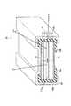
本発明の第1の実施の形態に係る半導体発光素子1の模式的鳥瞰構造は、図1に示すように表される。また、第1の実施の形態に係る半導体発光素子1を実装基板32上に搭載する様子を示す模式的鳥瞰構造は、図2に示すように表される。また、第1の実施の形態に係る半導体発光素子1を実装基板32上に搭載した模式的断面構造は、図3に示すように表される。(First embodiment)
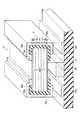
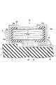
A schematic bird's-eye view structure of the semiconductor light emitting device 1 according to the first embodiment of the present invention is expressed as shown in FIG. Also, a schematic bird's-eye view showing a state in which the semiconductor light emitting device 1 according to the first embodiment is mounted on the
第1の実施の形態に係る半導体発光素子1は、図1に示すように、基板10と、基板10上に配置されたエピタキシャル成長層8と、エピタキシャル成長層8上に配置された表面電極層20と、基板10の裏面に配置された裏面電極層22と、基板10の側面42aに沿って形成され、基板10、エピタキシャル成長層8からなる第1側壁面および表面電極層20の表面および裏面電極層22の表面上に延在して配置された第1絶縁層24aと、第1絶縁層24a上および表面電極層20上の一部に配置された第1電極層26aとを備える。 As shown in FIG. 1, the semiconductor light emitting device 1 according to the first embodiment includes a
また、図1に示すように、基板10の側面42aに対向して並行に形成された側面42bに沿って形成され、基板10、エピタキシャル成長層8からなる第2側壁面および表面電極層20の表面および裏面電極層22の表面上に延在して配置された第2絶縁層24bと、第2絶縁層24b上および表面電極層20上の一部に配置された第2電極層26bとを備える。 Further, as shown in FIG. 1, the
図1において、第1の実施の形態に係る半導体発光素子1からの発光は、図中のhνで示すように等方的に発光される。 In FIG. 1, light emitted from the semiconductor light emitting device 1 according to the first embodiment is emitted isotropically as indicated by hv in the figure.
また、図2および図3に示すように、第1電極層26aおよび第2電極層26bは、それぞれアノード電極30aおよびアノード電極30bに接続され、裏面電極層22は、カソード電極28に接続される。 As shown in FIGS. 2 and 3, the
また、図2および図3に示すように、アノード電極30a、アノード電極30bおよびカソード電極28は、実装基板32上に配置されている。アノード電極30aおよびアノード電極30bは、電気的に共通に接続されている。 As shown in FIGS. 2 and 3, the
第1電極層26aおよび第2電極層26bは、それぞれアノード電極30aおよびアノード電極30bにダイボンディングによって接続され、裏面電極層22は、カソード電極28にダイボンディングによって接続される。 The
第1電極層26a、第2電極層26bの一方若しくは両方は、例えば、Auなどの薄膜金属層若しくは透明電極層を備えていても良い。透明電極層としては、例えば、ITO、ITZO、ZnOなどを適用することができる。 One or both of the
エピタキシャル成長層8は、基板10上に配置された第1クラッド層12と、第1クラッド層12上に配置された多重量子井戸(MQW:Multi-Quantum Well)層14と、MQW層14上に配置された第2クラッド層16とを備える。さらに、第2クラッド層16上には、ウィンドウ層18を備えていても良い。また、ウィンドウ層18の表面上は、光の取り出し効率を高めるために、フロスト処理を実施しても良い。 The
ここで、例えば、基板10はGaAsで形成され、第1クラッド層12および第2クラッド層16は、AlInGaP層で形成され、MQW層14は、InGaP/AlInGaPのペアで形成されている。 Here, for example, the
表面電極層20は透明電極であり、例えば、ITO、IZTO、ZnOで形成される。裏面電極層22は、例えばAu層で形成されている。 The
第1絶縁層24a、第2絶縁層24bの一方若しくは両方は、シリコン絶縁膜、シリコン窒化膜などによって形成される。 One or both of the first
また、第1絶縁層24a、第2絶縁層24bの一方若しくは両方は、分布ブラック反射(DBR:Distributed Bragg Reflector)層を備えていても良い。DBR層としては、ZrO2、Al2O3、SiO2 、TiO2、Ta2O5、Nb2O5、AlN、SiN、AlON、SiON、AlNx(0<x<1)いずれかを含む多層膜によって形成されていてもよい。ここで、AlNx(0<x<1)は、AlNのストイキオメトリ制御からずれている組成比の場合を示す。One or both of the
また、DBR層は、高光反射特性を有し、例えば、ZrO2膜とSiO2膜からなる積層構造を備えていてもよい。ZrO2膜の厚さd1およびSiO2膜の厚さd2は、d1=λ/4n1、d2=λ/4n2となるように形成する。ここで、n1はZrO2膜の屈折率2.18であり、n2はSiO2膜の屈折率1.46である。Further, the DBR layer has a high light reflection characteristic, and may have a laminated structure including, for example, a ZrO2 film and a SiO2 film. The thickness d1 of the ZrO2 film and the thickness d2 of the SiO2 film are formed such that d1 = λ / 4n1 and d2 = λ / 4n2 . Here, n1 is the refractive index 2.18 of the ZrO2 film, and n2 is the refractive index 1.46 of the SiO2 film.
また、第1絶縁層24a、第2絶縁層24bの一方若しくは両方は、酸素吸収層を備えていても良い。酸素吸収層としては、ZrO2、Al2O3、SiO2 、TiO2、Ta2O5、Nb2O5、AlN、SiN、AlON、SiON、AlNx(0<x<1)いずれかを含む層が適用可能である。One or both of the first insulating
(製造方法)
第1の実施の形態に係る半導体発光素子の製造方法は、基板10上にエピタキシャル成長層8を形成する工程と、エピタキシャル成長層8上に表面電極層20を形成する工程と、基板10の裏面に裏面電極層22を形成する工程と、基板10の側面42aに沿って形成され、基板10、エピタキシャル成長層8からなる第1側壁面および表面電極層20の表面上および裏面電極層22の表面上に延在して第1絶縁層24aを形成する工程と、基板10の側面42aに対向して並行に形成された側面42bに沿って形成され、基板10、エピタキシャル成長層8からなる第2側壁面および表面電極層20の表面および裏面電極層22の表面上に延在して第2絶縁層24bを形成する工程と、第1絶縁層24a上および表面電極層20上の一部に第1電極層26aを形成する工程と、第2絶縁層24b上および表面電極層20上の一部に第2電極層26bを形成する工程とを有する。(Production method)
The method for manufacturing a semiconductor light emitting device according to the first embodiment includes a step of forming an
また、アノード電極30およびカソード電極28を実装基板32上に形成する工程と、第1電極層26aおよび第2電極層26bの一方若しくは両方をそれぞれアノード電極30aおよび30bに接続し、裏面電極層22をカソード電極28に接続する工程とを有する。 Further, the step of forming the
第1の実施の形態に係る半導体発光素子の製造方法において、ウェハプロセスの一工程を示す模式的断面構造は、図4(a)〜図4(d)に示すように表される。また、LEDウェハ34を劈開面にそって劈開する様子を示す模式的鳥瞰構造、およびLEDウェハ34を劈開面にそって劈開して形成された複数のLEDバー36の模式的鳥瞰構造は、それぞれ図5(a)および図5(b)に示すように表される。 In the method for manufacturing a semiconductor light emitting device according to the first embodiment, a schematic cross-sectional structure showing one step of the wafer process is expressed as shown in FIGS. 4 (a) to 4 (d). In addition, a schematic bird's-eye view structure showing how the
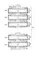
また、LEDバー36とシリコンバー40を複数積層化した積層化構造50をLEDバー固定装置38に挿入する一工程を示す模式的鳥瞰構造は、図6に示すように表される。 Further, a schematic bird's-eye view structure showing one step of inserting the
また、LEDバー36とシリコンバー40を複数積層化した積層化構造50を形成する一工程を示す模式的断面構造は、図7に示すように表される。 Further, a schematic cross-sectional structure showing one step of forming a
第1の実施の形態に係る半導体発光素子の製造方法に使用するシリコンバー40の模式的鳥瞰構造は、図8に示すように表される。 A schematic bird's-eye view structure of the
積層化されたLEDバー36の側壁、表面電極層20の一部および裏面電極層22の一部に第1絶縁層24a、第2絶縁層24bを形成する工程を示す模式的断面構造は、図9に示すように表される。 The schematic cross-sectional structure showing the process of forming the first insulating
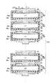
図9の工程後、LEDバー36と反転されたシリコンバー40を積層する一工程を示す模式的断面構造は、図10に示すように表される。 A schematic cross-sectional structure showing one step of laminating the
積層化されたLEDバー36の第1絶縁層24a、第2絶縁層24b上および表面電極層20の一部に第1電極層26a、第2電極層26bを形成する工程を示す模式的断面構造は、図11に示すように表される。 Schematic sectional structure showing a step of forming the
第1の実施の形態に係る半導体発光素子の製造方法を以下に説明する。 A method for manufacturing the semiconductor light emitting device according to the first embodiment will be described below.
(a)まず、図4(a)に示すように、GaAs基板10上に、分子線エピタキシャル成長法(MBE:Molecular Beam Epitaxy)、MOCVD(Metal Organic Chemical Vapor Deposition)法などを用いて、第1クラッド層12、MQW層14、第2クラッド層16およびウィンドウ層18を順次形成する。(A) First, as shown in FIG. 4A, a first cladding is formed on a
(b)次に、図4(b)に示すように、ウィンドウ層18上に表面電極層20をスパッタリング法、真空蒸着法などを用いて形成する。表面電極層20の材料としては、透明導電膜であることが望ましい。例えば、薄いチタン層およびAu層などを用いて形成することができる。また、ITO、IZTO、ZnOなどを用いて形成することができる。(B) Next, as shown in FIG. 4B, the
(c)次に、図4(c)に示すように、GaAs基板10を裏面から薄層化する。この薄層化の工程は、例えば、ラッピング、ポリッシング、化学的機械的研磨(CMP:Chemical Mechanical Polishing)技術、エッチング技術などによって実施することができる。結果として、例えば、基板10の厚さを約90μmに形成することができる。厚さはこれに限るものではなく、約30μm〜250μm程度のいずれかとする。(C) Next, as shown in FIG. 4C, the
(d)次に、図4(d)に示すように、基板10上に、裏面電極層22をスパッタリング法、真空蒸着法などを用いて形成する。裏面電極層22の材料としては、例えば、Au層、或いはAu/AuGe−Ni合金/Auからなる積層構造を用いることができる。(D) Next, as shown in FIG. 4D, the
(e)次に、図5(a)に示すように、LEDウェハ34を劈開面に沿って劈開する。その結果、図5(b)に示すように、幅W、長さLを有する複数のLEDバー36を形成することができる。なお、劈開に限らず、ダイシング、スクライブでも可能である。(E) Next, as shown in FIG. 5A, the
(f)次に、図6に示すように、LEDバー36とシリコンバー40を複数積層化した積層化構造50をLEDバー固定装置38に挿入する。ここで、積層化構造50の詳細構造は、図7に示すように表される。シリコンバー40の構造は、図8に示すように、凸型形状を備えるため、積層化構造50において、表面電極層20の一部分と裏面電極層22の一部分は、シリコンバー40によって被覆されている。(F) Next, as shown in FIG. 6, a
(g)次に、積層化構造50をLEDバー固定装置38に挿入した状態で、図9に示すように、スパッタリング法によって、第1絶縁層24aおよび第2絶縁層24bを形成する。すなわち、W3の幅だけ表面電極層20の表面上にそれぞれ第1絶縁層24a、第2絶縁層24bが形成される。また、W2+W3の幅だけ裏面電極層22の表面上にそれぞれ第1絶縁層24a、第2絶縁層24bが形成される。ここで、LEDバー36の幅Wに対して、W−(W1+2W2)=2W3の関係を有する。なお、図9において、シリコンバー40の側壁面上にも絶縁層が形成されるが、説明を簡単化するため、図示を省略している。(G) Next, with the
(h)次に、図10に示すように、LEDバー36と反転されたシリコンバー40を複数積層化して、積層化構造50aを形成する。なお、図10において使用するシリコンバー40は、必ずしも図9において使用したシリコンバー40を適用する必要はなく、電極層を形成する幅の寸法に応じて、別の寸法を有するシリコンバーを適宜選択可能である。また、シリコンバー40ではなく、LEDバー36を反転させるようにしても良い。(H) Next, as shown in FIG. 10, a plurality of LED bars 36 and inverted silicon bars 40 are stacked to form a
(i)次に、積層化構造50aをLEDバー固定装置38に挿入した状態で、図11に示すように、第1電極層26aおよび第2電極層26bをスパッタリング法、真空蒸着法などを用いて形成する。すなわち、W2+W3の幅だけ表面電極層20の表面上にそれぞれ第1電極層26a、第2電極層26bが形成される。W2の幅で、第1電極層26a、第2電極層26bは、表面電極層20と接続されている。また、W3の幅だけ裏面電極層22の表面上にそれぞれ第1電極層26a、第2電極層26bが形成される。ここで、図8に示されるシリコンバー40の厚さD1、D2は、スパッタリング法、真空蒸着法などを用いて形成する第1電極層26aおよび第2電極層26bの回り込みを充分に確保できる程度の厚さを備えていれば良い。また、図11において、シリコンバー40の側壁面上にも電極層が形成されるが、説明を簡単化するため、図示を省略している。(I) Next, in a state where the
(j)次に、積層化構造50aをLEDバー固定装置38から取り外し、シリコンバー40を取り外す。LEDバー36を分割して、結果として、図1に示される第1の実施の形態に係る半導体発光素子1を得る。(J) Next, the
(k)次に、図2に示すように、実装基板32上にアノード電極30aおよびアノード電極30b、およびカソード電極28を真空蒸着法、スパッタリング法などを用いて形成し、所定のストライプ形状などにパターニングする。(K) Next, as shown in FIG. 2, the
(l)次に、図3に示すように、実装基板32上に半導体発光素子1を載置し、アノード電極30aおよびアノード電極30bをそれぞれ第1電極層26aおよび第2電極層26b、カソード電極28を裏面電極層22にダイボンディングによって接続する。(L) Next, as shown in FIG. 3, the semiconductor light emitting device 1 is mounted on the mounting
第1の実施の形態によれば、エピタキシャル成長層8上には、光を透過させない金属電極が存在しないため、光のロスを低減することができ、光の取り出し効率を改善することができる。 According to the first embodiment, since there is no metal electrode that does not transmit light on the
第1の実施の形態によれば、半導体発光素子の組み立て時にワイヤボンディングが不要となるため、パッケージを薄くすることができる。 According to the first embodiment, since the wire bonding is not required when assembling the semiconductor light emitting device, the package can be thinned.
第1の実施の形態によれば、半導体発光素子の製造方法が簡略化されるため、チップ化までの製造工程に要する時間を短縮することができる。 According to the first embodiment, since the method for manufacturing a semiconductor light emitting device is simplified, the time required for the manufacturing process up to chip formation can be shortened.
第1の実施の形態によれば、第1絶縁層24a、第1電極層26aおよび第2絶縁層24b、第2電極層26bの膜厚を変化させて、反射率を変化させることによって、発光の指向性を変化させることもできる。 According to the first embodiment, light is emitted by changing the film thickness of the first insulating
第1の実施の形態によれば、第1電極層26aおよび第2電極層26bを光を透過させない金属電極層として形成することによって、側壁面への光の出射を抑制することもできる。 According to the first embodiment, by forming the
第1の実施の形態によれば、光の取り出し効率が改善され、かつ薄型パッケージ化の容易な半導体発光素子およびその製造方法を提供することができる。 According to the first embodiment, it is possible to provide a semiconductor light emitting device with improved light extraction efficiency and easy thin packaging and a method for manufacturing the same.
(変形例)
第1の実施の形態の変形例1に係る半導体発光素子を実装基板上に搭載した模式的断面構造は、図12(a)に示すように表され、変形例2に係る半導体発光素子を実装基板上に搭載した模式的断面構造は、図12(b)に示すように表される。(Modification)
A schematic cross-sectional structure in which the semiconductor light emitting element according to the first modification of the first embodiment is mounted on a mounting substrate is represented as shown in FIG. 12A, and the semiconductor light emitting element according to the second modification is mounted. A schematic cross-sectional structure mounted on the substrate is expressed as shown in FIG.
第1の実施の形態の変形例1に係る半導体発光素子1aは、第1絶縁層24a上および表面電極層20の表面上の一部に配置された第1電極層26aのみを備え、第2絶縁層24bおよび第2電極層26bを備えていない。一方、第1の実施の形態の変形例2に係る半導体発光素子1aは、第1絶縁層24a上および表面電極層20の表面上の一部に配置された第1電極層26aおよび第2絶縁層24bのみを備え、第2絶縁層24b上には第2電極層26bを備えていない。 The semiconductor
第1の実施の形態の変形例1および変形例2に係る半導体発光素子1aは、電極層を対向する側面の片側にのみ設けることによって、第1の実施の形態に係る半導体発光素子1に比べて、光の取り出し効率が改善される。 The semiconductor
また、第1の実施の形態の変形例2に係る半導体発光素子1aは、第2絶縁層24bを誘電体多層膜として形成することによって、反射率を調整しても良い。 Further, in the semiconductor
第1の実施の形態の変形例1および変形例2においては、アノード電極30aと第1電極層26a間は、半田層44によって、半田付けされている。 In the first and second modifications of the first embodiment, the
第1の実施の形態の変形例1および変形例2によれば、光の取り出し効率が改善され、かつ薄型パッケージ化の容易な半導体発光素子およびその製造方法を提供することができる。 According to Modification 1 and Modification 2 of the first embodiment, it is possible to provide a semiconductor light-emitting element that can improve light extraction efficiency and can be easily formed into a thin package, and a method for manufacturing the same.
(第2の実施の形態)
第2の実施の形態に係る半導体発光素子1bの模式的鳥瞰構造は、図13に示すように表される。また、第2の実施の形態に係る半導体発光素子1bを実装基板32上に搭載する様子を示す模式的鳥瞰構造は、図14に示すように表される。また、第2の実施の形態に係る半導体発光素子1bを実装基板32上に搭載した模式的断面構造は、図15に示すように表される。(Second Embodiment)
A schematic bird's-eye view structure of the semiconductor
第2の実施の形態に係る半導体発光素子は、図13に示すように、基板10と、基板10上に配置されたエピタキシャル成長層8と、エピタキシャル成長層8上に配置された表面電極層20と、基板10の裏面に配置された裏面電極層22と、基板10の側面42aに沿って形成され、基板10、エピタキシャル成長層8からなる第1側壁面および表面電極層20の表面上および裏面電極層22の表面上に延在して配置された第1絶縁層24aと、基板10の側面42aに対向して並行に形成された側面42bに沿って形成され、基板10、エピタキシャル成長層8からなる第2側壁面および表面電極層20の表面上および裏面電極層22の表面上に延在して配置された第2絶縁層24bと、第1絶縁層24aおよび第2絶縁層24b上および表面電極層20上に配置された第1電極層26とを備える。なお、図13において、第1電極層26は、LEDバー36の配置によっては、若干下面に回り込みが生ずることもある。また、回り込みがないように作成することもできる。 As shown in FIG. 13, the semiconductor light emitting device according to the second embodiment includes a
図13において、第2の実施の形態に係る半導体発光素子1bからの発光は、図中のhνで示すように等方的に発光される。 In FIG. 13, the light emitted from the semiconductor
図14および図15に示すように、第1電極層26は、アノード電極30に接続され、裏面電極層22は、カソード電極28に接続される。 As shown in FIGS. 14 and 15, the
図14および図15に示すように、アノード電極30およびカソード電極28は、実装基板32上に配置され、アノード電極30と第1電極層26は半田層44によって半田付けされていても良い。 As shown in FIGS. 14 and 15, the
エピタキシャル成長層8は、基板10上に配置された第1クラッド層12と、第1クラッド層12上に配置されたMQW層14と、MQW層14上に配置された第2クラッド層16を備える。さらに、第2クラッド層16上にウィンドウ層18を備えていても良い。 The
ここで、例えば、基板10はGaAsで形成され、第1クラッド層12および第2クラッド層16は、AlInGaP層で形成され、MQW層14は、InGaP/AlInGaPのペアで形成されている。 Here, for example, the
基板10の裏面には、裏面電極層22が配置され、ウィンドウ層18の表面には、表面電極層20が配置されている。表面電極層20は透明電極であり、例えば、ITO、IZTO、ZnOで形成される。裏面電極層22は、例えばAu層で形成されている。 A
第1絶縁層24a、第2絶縁層24bの一方若しくは両方は、シリコン絶縁膜、シリコン窒化膜などによって形成される。 One or both of the first insulating
また、第1絶縁層24a、第2絶縁層24bの一方若しくは両方は、DBR層を備えていても良い。DBR層の例は第1の実施の形態と同様である。 One or both of the first insulating
また、第1電極層26は透明電極層を備える。透明電極層の例は第1の実施の形態と同様である。 The
第1の実施の形態においては、第1絶縁層24aおよび第2絶縁層24bの成膜時と、第1電極層26aおよび第2電極層26bの成膜時の2回、LEDバー36の積み上げ工程が必要であったが、第2の実施の形態においては、第1絶縁層24aおよび第2絶縁層24bの成膜時のみLEDバー36の積み上げ工程が必要であり、第1電極層26aおよび第2電極層26bは、共通の電極層26として形成されるため、LEDバー36の積み上げ工程は不要である。 In the first embodiment, the
(製造方法)
第2の実施の形態に係る半導体発光素子の製造方法は、基板10上にエピタキシャル成長層8を形成する工程と、エピタキシャル成長層8上に表面電極層20を形成する工程と、基板10の裏面に裏面電極層22を形成する工程と、基板10の側面42aに沿って形成され、基板10、エピタキシャル成長層8からなる第1側壁面および表面電極層20の表面上および裏面電極層22の表面上に延在して第1絶縁層24aを形成する工程と、基板10の側面42aに対向して並行に形成された側面42bに沿って形成され、基板10、エピタキシャル成長層8からなる第2側壁面および表面電極層20の表面上および裏面電極層22の表面上に延在して第2絶縁層24bを形成する工程と、第1絶縁層24aおよび第2絶縁層24b上および表面電極層20の上に第1電極層26を形成する工程とを備える。(Production method)
The method for manufacturing a semiconductor light emitting device according to the second embodiment includes a step of forming the
また、アノード電極30およびカソード電極28を実装基板32上に形成する工程と、第1電極層26をアノード電極30と半田付けによって接続し、裏面電極層22をカソード電極28に接続する工程とを有する。 Also, a step of forming the
その他各部の詳細な製造工程は、第1の実施の形態と同様であるため、重複説明は省略する。 Since the detailed manufacturing process of each other part is the same as that of 1st Embodiment, duplication description is abbreviate | omitted.
第1電極層26を形成する工程は、第1絶縁層24aおよび第2絶縁層24bを形成したLEDバー36を平面台に並べて配置し、例えば、パルスレーザデポジション(PLD:Pulse Laser Deposition)法を用いて、例えばZnO電極を成膜することによって、形成することができる。したがって、シリコンバー40の配置が不要となり、製造工程は簡単化される。なお、ZnO電極は、LEDバー36の配置によっては、図13に示すように、若干下面に回りこむ。また、回り込みがないように作成することもできる。 In the step of forming the
第2の実施の形態によれば、光の取り出し効率が改善され、かつ薄型パッケージ化の容易な半導体発光素子およびその製造方法を提供することができる。 According to the second embodiment, it is possible to provide a semiconductor light emitting device with improved light extraction efficiency and easy packaging, and a method for manufacturing the same.
(その他の実施の形態)
上記のように、本発明は第1〜第2の実施の形態によって記載したが、この開示の一部をなす論述および図面はこの発明を限定するものであると理解すべきではない。この開示から当業者には様々な代替実施の形態、実施例および運用技術が明らかとなろう。(Other embodiments)
As described above, the present invention has been described according to the first to second embodiments. However, it should not be understood that the description and drawings constituting a part of this disclosure limit the present invention. From this disclosure, various alternative embodiments, examples and operational techniques will be apparent to those skilled in the art.
第1〜第2の実施の形態においては、基板10および第1クラッド層12の導電型をn型とし、第2クラッド層16およびウィンドウ層18の導電型をp型とする例が開示されているが、これらの導電型を反対にしても良い。この場合、アノード電極とカソード電極は逆の構成となり、表面電極層20に接続される第1電極層、第2電極層がカソード電極に接続され、裏面電極層22は、アノード電極に接続される。 In the first to second embodiments, examples are disclosed in which the conductivity type of the
第1〜第2の実施の形態においては、基板10とクラッド層12の間にDBR層を設けても良い。 In the first and second embodiments, a DBR layer may be provided between the
第1〜第2の実施の形態においては、基板10として、主として、GaAs基板を適用する例が開示されているが、Si基板、SiC基板、GaP基板、サファイア基板などを適用することも可能である。 In the first to second embodiments, an example in which a GaAs substrate is mainly applied as the
第1クラッド層12および第2クラッド層16は、例えばAlGaAs層によって形成され、MQW層14は、例えばGaAs/GaAlAs層からなるヘテロ接合ペアを積層して形成しても良い。または、GaN系発光素子を形成しても良い。 The
シリコンバー40は、シリコンに限らず、他の材料を用いて形成したバーであっても良い。 The
このように、本発明はここでは記載していない様々な実施の形態等を含むことは勿論である。したがって、本発明の技術的範囲は上記の説明から妥当な特許請求の範囲に係る発明特定事項によってのみ定められるものである。 As described above, the present invention naturally includes various embodiments not described herein. Therefore, the technical scope of the present invention is defined only by the invention specifying matters according to the scope of claims reasonable from the above description.
本発明の半導体発光素子およびその製造方法は、GaAs基板、Si基板、SiC基板、GaP基板、サファイア基板等を有するLED素子等の半導体発光素子全般に利用可能である。 The semiconductor light emitting device and the manufacturing method thereof of the present invention can be used for all semiconductor light emitting devices such as LED devices having a GaAs substrate, Si substrate, SiC substrate, GaP substrate, sapphire substrate and the like.
1、1a、1b…半導体発光素子
8…エピタキシャル成長層
10…基板
12…n型クラッド層
14…多重量子井戸(MQW)層
16…p型クラッド層
18…ウィンドウ層
20…表面電極層
22…裏面電極層
24a、24b…絶縁層
26、26a、26b…電極層
28…カソード電極
30、30a、30b…アノード電極
32…実装基板
34…LEDウェハ
36…LEDバー
38…LEDバー固定装置
40…シリコンバー
42a、42b…側面
44…半田層
50、50a…積層化構造DESCRIPTION OF
Claims (17)
Translated fromJapanese前記基板上に配置されたエピタキシャル成長層と、
前記エピタキシャル成長層上に配置された表面電極層と、
前記基板の裏面に配置された裏面電極層と、
前記基板の側面に沿って形成され、前記基板、前記エピタキシャル成長層からなる第1側壁面および前記表面電極層の表面上および前記裏面電極層の表面上に延在して配置された第1絶縁層と、
前記表面電極上から前記第1絶縁層の表面上、側面上を介して前記第1絶縁層の裏面上まで渡って形成された第1電極層と
を備えることを特徴とする半導体発光素子。A substrate,
An epitaxially grown layer disposed on the substrate;
A surface electrode layer disposed on the epitaxial growth layer;
A back electrode layer disposed on the back surface of the substrate;
A first insulating layer formed along the side surface of the substrate and extending on the surface of the substrate, the first sidewall surface comprising the epitaxially grown layer, the surface electrode layer, and the surface of the back electrode layer When,
And a first electrode layerformed over the surface of the first insulating layer, the surface of the first insulating layer, the side of the first insulating layer, and the back surface of the first insulating layer .
前記表面電極上から前記第2絶縁層の表面上、側面上を介して前記第2絶縁層の裏面上まで渡って形成された第2電極層と
を備えることを特徴とする請求項1に記載の半導体発光素子。Formed along the side surface formed in parallel to the side surface of the substrate, on the substrate, the second side wall surface comprising the epitaxial growth layer, the surface of the surface electrode layer, and the surface of the back electrode layer A second insulating layer disposed extending;
The second electrode layerformed over the surface electrode, the surface of the second insulating layer, the side surface, and the back surface of the second insulating layer. Semiconductor light emitting device.
前記基板上に配置されたエピタキシャル成長層と、
前記エピタキシャル成長層上に配置された表面電極層と、
前記基板の裏面に配置された裏面電極層と、
前記基板の側面に沿って形成され、前記基板、前記エピタキシャル成長層からなる第1側壁面および前記表面電極層の表面上および前記裏面電極層の表面上に延在して配置された第1絶縁層と、
前記基板の前記側面に対向して並行に形成された側面に沿って形成され、前記基板、前記エピタキシャル成長層からなる第2側壁面および前記表面電極層の表面上および前記裏面電極層の表面上に延在して配置された第2絶縁層と、
前記表面電極上から前記第1絶縁層の表面上、側面上を介して前記第1絶縁層の裏面上まで渡って、および前記表面電極上から前記第2絶縁層の表面上、側面上を介して前記第2絶縁層の裏面上まで渡って形成された第1電極層と
を備えることを特徴とする半導体発光素子。A substrate,
An epitaxially grown layer disposed on the substrate;
A surface electrode layer disposed on the epitaxial growth layer;
A back electrode layer disposed on the back surface of the substrate;
A first insulating layer formed along the side surface of the substrate and extending on the surface of the substrate, the first sidewall surface comprising the epitaxially grown layer, the surface electrode layer, and the surface of the back electrode layer When,
Formed along the side surface formed in parallel to the side surface of the substrate, on the substrate, the second side wall surface comprising the epitaxial growth layer, the surface of the surface electrode layer, and the surface of the back electrode layer A second insulating layer disposed extending;
From the surface electrode to the surface of the first insulating layer, over the side surface to the back surface of the first insulating layer, andfrom the surface electrode to the surface of the second insulating layer, on the side surface. And a first electrode layerformed over the back surface of the second insulating layer .
前記エピタキシャル成長層上に表面電極層を形成する工程と、
前記基板の裏面に裏面電極層を形成する工程と、
前記基板の側面に沿って形成され、前記基板、前記エピタキシャル成長層からなる第1側壁面および前記表面電極層の表面上および前記裏面電極層の表面上に延在して第1絶縁層を形成する工程と、
前記基板の前記側面に対向して並行に形成された側面に沿って形成され、前記基板、前記エピタキシャル成長層からなる第2側壁面および前記表面電極層の表面上および前記裏面電極層の表面上に延在して第2絶縁層を形成する工程と、
前記表面電極上から前記第1絶縁層の表面上、側面上を介して前記第1絶縁層の裏面上まで渡って第1電極層を形成する工程と、
前記表面電極上から前記第2絶縁層の表面上、側面上を介して前記第2絶縁層の裏面上まで渡って第2電極層を形成する工程と
を有することを特徴とする半導体発光素子の製造方法。Forming an epitaxially grown layer on the substrate;
Forming a surface electrode layer on the epitaxial growth layer;
Forming a back electrode layer on the back surface of the substrate;
A first insulating layer is formed along a side surface of the substrate and extends on the substrate, the first sidewall surface made of the epitaxial growth layer, the surface of the front electrode layer, and the surface of the back electrode layer. Process,
Formed along the side surface formed in parallel to the side surface of the substrate, on the substrate, the second side wall surface comprising the epitaxial growth layer, the surface of the surface electrode layer, and the surface of the back electrode layer Extending a second insulating layer; and
Forming a first electrode layerover the surface electrode from the surface of the first insulating layer to the back surface of the first insulating layer via the side surface;
Forming a second electrode layerover the surface electrode, the surface of the second insulating layer, the side surface, and the back surface of the second insulating layer . Production method.
前記第1電極層および前記第2電極層の一方若しくは両方を前記アノード電極に接続し、前記裏面電極層を前記カソード電極に接続する工程と
を有することを特徴とする請求項14に記載の半導体発光素子の製造方法。Forming an anode electrode and a cathode electrode on a mounting substrate;
The method according to claim 14, further comprising: connecting one or both of the first electrode layer and the second electrode layer to the anode electrode and connecting the back electrode layer to the cathode electrode. Manufacturing method of light emitting element.
前記エピタキシャル成長層上に表面電極層を形成する工程と、
前記基板の裏面に裏面電極層を形成する工程と、
前記基板の側面に沿って形成され、前記基板、前記エピタキシャル成長層からなる第1側壁面および前記表面電極層の表面上および前記裏面電極層の表面上に延在して第1絶縁層を形成する工程と、
前記基板の前記側面に対向して並行に形成された側面に沿って形成され、前記基板、前記エピタキシャル成長層からなる第2側壁面および前記表面電極層の表面上および前記裏面電極層の表面上に延在して第2絶縁層を形成する工程と、
前記表面電極上から前記第1絶縁層の表面上、側面上を介して前記第1絶縁層の裏面上まで渡って、および前記表面電極上から前記第2絶縁層の表面上、側面上を介して前記第2絶縁層の裏面上まで渡って第1電極層を形成する工程と
を備えることを特徴とする半導体発光素子の製造方法。Forming an epitaxially grown layer on the substrate;
Forming a surface electrode layer on the epitaxial growth layer;
Forming a back electrode layer on the back surface of the substrate;
A first insulating layer is formed along a side surface of the substrate and extends on the substrate, the first sidewall surface made of the epitaxial growth layer, the surface of the front electrode layer, and the surface of the back electrode layer. Process,
Formed along the side surface formed in parallel to the side surface of the substrate, on the substrate, the second side wall surface comprising the epitaxial growth layer, the surface of the surface electrode layer, and the surface of the back electrode layer Extending a second insulating layer; and
From the surface electrode to the surface of the first insulating layer, over the side surface to the back surface of the first insulating layer, andfrom the surface electrode to the surface of the second insulating layer, on the side surface. And a step of forming a first electrode layerover the back surface of the second insulating layer .
前記第1電極層を前記アノード電極と半田付けによって接続し、前記裏面電極層を前記カソード電極に接続する工程と
を有することを特徴とする請求項16に記載の半導体発光素子の製造方法。Forming an anode electrode and a cathode electrode on a mounting substrate;
The method according to claim 16, further comprising: connecting the first electrode layer to the anode electrode by soldering and connecting the back electrode layer to the cathode electrode.
Priority Applications (1)
| Application Number | Priority Date | Filing Date | Title |
|---|---|---|---|
| JP2009106875AJP5277066B2 (en) | 2009-04-24 | 2009-04-24 | Semiconductor light emitting device and manufacturing method thereof |
Applications Claiming Priority (1)
| Application Number | Priority Date | Filing Date | Title |
|---|---|---|---|
| JP2009106875AJP5277066B2 (en) | 2009-04-24 | 2009-04-24 | Semiconductor light emitting device and manufacturing method thereof |
Publications (2)
| Publication Number | Publication Date |
|---|---|
| JP2010258230A JP2010258230A (en) | 2010-11-11 |
| JP5277066B2true JP5277066B2 (en) | 2013-08-28 |
Family
ID=43318796
Family Applications (1)
| Application Number | Title | Priority Date | Filing Date |
|---|---|---|---|
| JP2009106875AExpired - Fee RelatedJP5277066B2 (en) | 2009-04-24 | 2009-04-24 | Semiconductor light emitting device and manufacturing method thereof |
Country Status (1)
| Country | Link |
|---|---|
| JP (1) | JP5277066B2 (en) |
Families Citing this family (4)
| Publication number | Priority date | Publication date | Assignee | Title |
|---|---|---|---|---|
| JP2012109162A (en) | 2010-11-18 | 2012-06-07 | Yazaki Corp | Connection structure of electronic component |
| KR101799450B1 (en)* | 2011-05-24 | 2017-11-20 | 엘지이노텍 주식회사 | A light emitting device and a light emitting device package |
| DE102015104886A1 (en)* | 2015-03-30 | 2016-10-06 | Osram Opto Semiconductors Gmbh | Optoelectronic semiconductor chip, optoelectronic semiconductor component and method for producing an optoelectronic semiconductor chip |
| US20220352418A1 (en)* | 2019-11-12 | 2022-11-03 | Sony Group Corporation | Semiconductor light emitting element and electronic apparatus |
Family Cites Families (5)
| Publication number | Priority date | Publication date | Assignee | Title |
|---|---|---|---|---|
| JP4236738B2 (en)* | 1998-08-27 | 2009-03-11 | 星和電機株式会社 | Manufacturing method of semiconductor device |
| JP4036658B2 (en)* | 2002-02-25 | 2008-01-23 | シャープ株式会社 | Nitride-based compound semiconductor laser device and manufacturing method thereof |
| JP4637566B2 (en)* | 2004-12-24 | 2011-02-23 | 京セラ株式会社 | Masking spacer and manufacturing method thereof |
| JP5486759B2 (en)* | 2006-04-14 | 2014-05-07 | 日亜化学工業株式会社 | Manufacturing method of semiconductor light emitting device |
| JP2008227002A (en)* | 2007-03-09 | 2008-09-25 | Nichia Chem Ind Ltd | Nitride semiconductor laser device |
- 2009
- 2009-04-24JPJP2009106875Apatent/JP5277066B2/ennot_activeExpired - Fee Related
Also Published As
| Publication number | Publication date |
|---|---|
| JP2010258230A (en) | 2010-11-11 |
Similar Documents
| Publication | Publication Date | Title |
|---|---|---|
| JP5024247B2 (en) | Light emitting element | |
| US8390018B2 (en) | Nitride-based compound semiconductor light emitting device and method of fabricating the same | |
| US8237180B2 (en) | Light emitting element including center electrode and thin wire electrode extending from periphery of the center electrode | |
| KR101017394B1 (en) | Light emitting device and method of manufacturing the same | |
| JP5776535B2 (en) | Group III nitride semiconductor light emitting device | |
| JP2011216882A (en) | High-efficiency light emitting diode, and method for fabricating the same | |
| US20120326118A1 (en) | Semiconductor light emitting device and method for manufacturing the same | |
| JP2011513954A (en) | Optoelectronic device and method of manufacturing optoelectronic device | |
| JP5277066B2 (en) | Semiconductor light emitting device and manufacturing method thereof | |
| JP2007324581A (en) | Integrated semiconductor light emitting device and method of manufacturing the same | |
| JP2005276899A (en) | Light-emitting element | |
| JP2004503096A (en) | InGaN based light emitting diode chip and method of manufacturing the same | |
| CN113130713A (en) | Light emitting element and method for manufacturing the same | |
| KR101154511B1 (en) | High efficiency light emitting diode and method of fabricating the same | |
| JP5326383B2 (en) | Light emitting device | |
| JP2009070893A (en) | Light-emitting device and manufacturing method therefor | |
| KR20130009719A (en) | High efficiency light emitting diode and method of fabricating the same | |
| JP2013206990A (en) | Vertical nitride semiconductor element and manufacturing method of the same | |
| JPH10321907A (en) | Light-emitting semiconductor element and its manufacture | |
| JP2007324579A (en) | Integrated semiconductor light emitting device and method of manufacturing the same | |
| JPH11340570A (en) | Photoelectric conversion element and its manufacture | |
| JP2012089801A (en) | Semiconductor light-emitting element, manufacturing method therefor, and package board | |
| JP5156347B2 (en) | Semiconductor light emitting device and manufacturing method thereof | |
| JP2009238845A (en) | Light-emitting module and method of manufacturing the same | |
| KR101138948B1 (en) | High efficiency light emitting diode |
Legal Events
| Date | Code | Title | Description |
|---|---|---|---|
| A621 | Written request for application examination | Free format text:JAPANESE INTERMEDIATE CODE: A621 Effective date:20120413 | |
| A977 | Report on retrieval | Free format text:JAPANESE INTERMEDIATE CODE: A971007 Effective date:20121219 | |
| A131 | Notification of reasons for refusal | Free format text:JAPANESE INTERMEDIATE CODE: A131 Effective date:20130108 | |
| A521 | Request for written amendment filed | Free format text:JAPANESE INTERMEDIATE CODE: A523 Effective date:20130307 | |
| TRDD | Decision of grant or rejection written | ||
| A01 | Written decision to grant a patent or to grant a registration (utility model) | Free format text:JAPANESE INTERMEDIATE CODE: A01 Effective date:20130423 | |
| A61 | First payment of annual fees (during grant procedure) | Free format text:JAPANESE INTERMEDIATE CODE: A61 Effective date:20130520 | |
| R150 | Certificate of patent or registration of utility model | Free format text:JAPANESE INTERMEDIATE CODE: R150 Ref document number:5277066 Country of ref document:JP Free format text:JAPANESE INTERMEDIATE CODE: R150 | |
| R250 | Receipt of annual fees | Free format text:JAPANESE INTERMEDIATE CODE: R250 | |
| R250 | Receipt of annual fees | Free format text:JAPANESE INTERMEDIATE CODE: R250 | |
| LAPS | Cancellation because of no payment of annual fees |