JP5274649B2 - Vacuum processing method and vacuum processing apparatus - Google Patents
Vacuum processing method and vacuum processing apparatusDownload PDFInfo
- Publication number
- JP5274649B2 JP5274649B2JP2011506082AJP2011506082AJP5274649B2JP 5274649 B2JP5274649 B2JP 5274649B2JP 2011506082 AJP2011506082 AJP 2011506082AJP 2011506082 AJP2011506082 AJP 2011506082AJP 5274649 B2JP5274649 B2JP 5274649B2
- Authority
- JP
- Japan
- Prior art keywords
- gas
- silicon substrate
- processing
- processing gas
- vacuum
- Prior art date
- Legal status (The legal status is an assumption and is not a legal conclusion. Google has not performed a legal analysis and makes no representation as to the accuracy of the status listed.)
- Active
Links
Images


Classifications
- H—ELECTRICITY
- H01—ELECTRIC ELEMENTS
- H01L—SEMICONDUCTOR DEVICES NOT COVERED BY CLASS H10
- H01L21/00—Processes or apparatus adapted for the manufacture or treatment of semiconductor or solid state devices or of parts thereof
- H01L21/02—Manufacture or treatment of semiconductor devices or of parts thereof
- H01L21/04—Manufacture or treatment of semiconductor devices or of parts thereof the devices having potential barriers, e.g. a PN junction, depletion layer or carrier concentration layer
- H01L21/18—Manufacture or treatment of semiconductor devices or of parts thereof the devices having potential barriers, e.g. a PN junction, depletion layer or carrier concentration layer the devices having semiconductor bodies comprising elements of Group IV of the Periodic Table or AIIIBV compounds with or without impurities, e.g. doping materials
- H01L21/30—Treatment of semiconductor bodies using processes or apparatus not provided for in groups H01L21/20 - H01L21/26
- H01L21/302—Treatment of semiconductor bodies using processes or apparatus not provided for in groups H01L21/20 - H01L21/26 to change their surface-physical characteristics or shape, e.g. etching, polishing, cutting
- H01L21/306—Chemical or electrical treatment, e.g. electrolytic etching
- H01L21/3065—Plasma etching; Reactive-ion etching
- H—ELECTRICITY
- H01—ELECTRIC ELEMENTS
- H01L—SEMICONDUCTOR DEVICES NOT COVERED BY CLASS H10
- H01L21/00—Processes or apparatus adapted for the manufacture or treatment of semiconductor or solid state devices or of parts thereof
- H01L21/02—Manufacture or treatment of semiconductor devices or of parts thereof
- H01L21/04—Manufacture or treatment of semiconductor devices or of parts thereof the devices having potential barriers, e.g. a PN junction, depletion layer or carrier concentration layer
- H01L21/18—Manufacture or treatment of semiconductor devices or of parts thereof the devices having potential barriers, e.g. a PN junction, depletion layer or carrier concentration layer the devices having semiconductor bodies comprising elements of Group IV of the Periodic Table or AIIIBV compounds with or without impurities, e.g. doping materials
- H01L21/30—Treatment of semiconductor bodies using processes or apparatus not provided for in groups H01L21/20 - H01L21/26
- H01L21/31—Treatment of semiconductor bodies using processes or apparatus not provided for in groups H01L21/20 - H01L21/26 to form insulating layers thereon, e.g. for masking or by using photolithographic techniques; After treatment of these layers; Selection of materials for these layers
- H01L21/3105—After-treatment
- H01L21/311—Etching the insulating layers by chemical or physical means
- H01L21/31105—Etching inorganic layers
- H01L21/31111—Etching inorganic layers by chemical means
- H01L21/31116—Etching inorganic layers by chemical means by dry-etching
- H—ELECTRICITY
- H01—ELECTRIC ELEMENTS
- H01L—SEMICONDUCTOR DEVICES NOT COVERED BY CLASS H10
- H01L21/00—Processes or apparatus adapted for the manufacture or treatment of semiconductor or solid state devices or of parts thereof
- H01L21/02—Manufacture or treatment of semiconductor devices or of parts thereof
- H01L21/02041—Cleaning
- H01L21/02043—Cleaning before device manufacture, i.e. Begin-Of-Line process
- H01L21/02046—Dry cleaning only
- H—ELECTRICITY
- H01—ELECTRIC ELEMENTS
- H01L—SEMICONDUCTOR DEVICES NOT COVERED BY CLASS H10
- H01L21/00—Processes or apparatus adapted for the manufacture or treatment of semiconductor or solid state devices or of parts thereof
- H01L21/02—Manufacture or treatment of semiconductor devices or of parts thereof
- H01L21/02041—Cleaning
- H01L21/02057—Cleaning during device manufacture
- H01L21/0206—Cleaning during device manufacture during, before or after processing of insulating layers
- H01L21/02063—Cleaning during device manufacture during, before or after processing of insulating layers the processing being the formation of vias or contact holes
- H—ELECTRICITY
- H01—ELECTRIC ELEMENTS
- H01L—SEMICONDUCTOR DEVICES NOT COVERED BY CLASS H10
- H01L21/00—Processes or apparatus adapted for the manufacture or treatment of semiconductor or solid state devices or of parts thereof
- H01L21/67—Apparatus specially adapted for handling semiconductor or electric solid state devices during manufacture or treatment thereof; Apparatus specially adapted for handling wafers during manufacture or treatment of semiconductor or electric solid state devices or components ; Apparatus not specifically provided for elsewhere
- H01L21/67005—Apparatus not specifically provided for elsewhere
- H01L21/67011—Apparatus for manufacture or treatment
- H01L21/67017—Apparatus for fluid treatment
- H01L21/67063—Apparatus for fluid treatment for etching
- H01L21/67069—Apparatus for fluid treatment for etching for drying etching
Landscapes
- Engineering & Computer Science (AREA)
- Physics & Mathematics (AREA)
- Microelectronics & Electronic Packaging (AREA)
- General Physics & Mathematics (AREA)
- Manufacturing & Machinery (AREA)
- Computer Hardware Design (AREA)
- Condensed Matter Physics & Semiconductors (AREA)
- Power Engineering (AREA)
- Chemical & Material Sciences (AREA)
- Chemical Kinetics & Catalysis (AREA)
- General Chemical & Material Sciences (AREA)
- Inorganic Chemistry (AREA)
- Plasma & Fusion (AREA)
- Drying Of Semiconductors (AREA)
- Cleaning Or Drying Semiconductors (AREA)
Description
Translated fromJapanese本発明は、真空状態の処理設備で処理を行う、例えば、エッチングを行う真空処理方法及び真空処理装置に関する。 The present invention relates to a vacuum processing method and a vacuum processing apparatus that perform processing, for example, etching, in processing equipment in a vacuum state.
半導体装置を製造する工程において、例えば、半導体基板(半導体ウエハ)のコンタクトホールの底部のウエハ上に形成された自然酸化膜(例えば、SiO2)を除去する必要がある。自然酸化膜を除去する技術として、ラジカル状態の水素(H*)とNF3ガスを使用するものが種々提案されている(例えば、特許文献1参照)。In the process of manufacturing a semiconductor device, for example, it is necessary to remove a natural oxide film (for example, SiO2 ) formed on a wafer at the bottom of a contact hole of a semiconductor substrate (semiconductor wafer). Various techniques using radical hydrogen (H* ) and NF3 gas have been proposed as techniques for removing the natural oxide film (see, for example, Patent Document 1).
特許文献1に開示された技術は、所定の真空状態にされた処理室内に処理ガスを導入し、所定の真空状態の雰囲気に配置されたシリコンウエハの酸化表面(SiO2)と反応させて反応生成物(NH4)2SiF6を生成する。その後、処理室を加熱してシリコン基板を所定温度に制御することにより、(NH4)2SiF6を昇華させてシリコン基板の表面の自然酸化膜を除去(エッチング)する技術である。The technique disclosed in
近年、自然酸化膜を除去したシリコンウエハの表面(単結晶シリコン、ポリシリコン)に対する清浄度合いに対する要求が高まっているのが現状であり、自然酸化膜を除去した後のシリコン面の更なる浄化性が要求されている。自然酸化膜との界面のシリコン面には、シリコンの格子間に酸素が存在していることも考えられ、自然酸化膜を除去した後であっても酸素が残存する虞がある。 In recent years, there is an increasing demand for the degree of cleanliness of the surface (single crystal silicon, polysilicon) of the silicon wafer from which the natural oxide film has been removed, and further purification of the silicon surface after the natural oxide film has been removed. Is required. It is conceivable that oxygen exists between the silicon lattices on the silicon surface at the interface with the natural oxide film, and oxygen may remain even after the natural oxide film is removed.
本発明は上記状況に鑑みてなされたもので、自然酸化膜を除去する処理装置を用い、自然酸化膜が除去された後に基板の面の酸素を確実に除去することができ、しかも、酸素除去で生じる虞のある副生成物を含めて除去することができる真空処理方法及び真空処理装置を提供することを目的とする。 The present invention has been made in view of the above situation, and a processing apparatus that removes a natural oxide film can be used to reliably remove oxygen on the surface of the substrate after the natural oxide film has been removed. An object of the present invention is to provide a vacuum processing method and a vacuum processing apparatus that can remove by-products that may be generated in the above.
上記目的を達成するための請求項1に係る本発明の真空処理方法は、処理ガスを導入し、所定の真空状態の雰囲気に配置されたシリコン基板の酸化表面と反応させ、反応生成物を生成し、シリコン基板を所定温度に制御することにより前記反応生成物を昇華させてシリコン基板の表面の酸化膜を除去し、酸化膜が除去された前記シリコン基板の配置を維持した状態で、補助処理ガスを導入して前記シリコン基板の表面にFラジカルを作用させ所定厚のシリコン層を除去し、シリコン層を除去した後、前記シリコン層の除去の際に生成された前記シリコン基板の表面の副生成物を除去することを特徴とする。 In order to achieve the above object, a vacuum processing method of the present invention according to
請求項1に係る本発明では、自然酸化膜が除去された後のシリコン基板の表層を補助処理ガスにより所定の厚さ除去し、自然酸化膜が除去された後に基板の面の酸素を確実に除去し、しかも、酸素除去で生じる虞のある副生成物を含めて除去することができる。 In the present invention according to
そして、請求項2に係る本発明の真空処理方法は、請求項1に記載の真空処理方法において、前記処理ガスを導入し、シリコン層が除去された前記シリコン基板の表面の副生成物と反応させて反応副生成物を生成し、シリコン基板を所定温度に制御することにより前記反応副生成物を昇華させてシリコン基板の表面の副生成物を除去することを特徴とする。 And the vacuum processing method of the present invention according to
請求項2に係る本発明では、自然酸化膜が除去された後のシリコン基板の表層を補助処理ガスにより所定の厚さ除去し、自然酸化膜を除去する処理装置を用い、自然酸化膜が除去された後に基板の面の酸素を確実に除去し、しかも、酸素除去で生じる虞のある副生成物を含めて除去することができる。 In the present invention according to
また、請求項3に係る本発明の真空処理方法は、請求項2に記載の真空処理方法において、シリコン層が除去された前記シリコン基板の配置を維持した状態で、前記シリコン基板の表面の副生成物を除去することを特徴とする。 According to a third aspect of the present invention, there is provided a vacuum processing method according to the second aspect of the present invention, in the vacuum processing method according to the second aspect, wherein the arrangement of the silicon substrate from which the silicon layer has been removed is maintained. It is characterized by removing the product.
請求項3に係る本発明では、酸素除去で生じる虞のある副生成物の除去まで自然酸化膜を除去する処理装置を用いて実施することができる。 The present invention according to
また、請求項4に係る本発明の真空処理方法は、請求項2もしくは請求項3に記載の真空処理方法において、前記処理ガスはNH3またはH2の少なくともいずれか一方とN2及びNF3であり、前記反応生成物及び前記反応副生成物を100℃〜400℃の雰囲気で昇華させ、前記補助処理ガスとして前記処理ガス、もしくは、N2とNF3を導入して前記シリコン基板の表面にFラジカルを作用させることを特徴とする。The vacuum processing method of the present invention according to
請求項4に係る本発明では、補助処理ガスとして処理ガス、もしくは、N2とNF3を導入してシリコン基板の表面にFラジカルを作用させることができる。In the present invention according to
また、請求項5に係る本発明の真空処理方法は、請求項4に記載の真空処理方法において、前記補助処理ガスを同一のガス導入手段から導入することを特徴とする。 The vacuum processing method of the present invention according to
請求項5に係る本発明では、同一のガス導入手段を用いて、補助処理ガスを導入してシリコン基板の表面にFラジカルを作用させることができる。 In the present invention according to
また、請求項6に係る本発明の真空処理方法は、請求項1に記載の真空処理方法において、無水フッ化水素酸ガス(AHF)とN2ガスとエタノール(C2H5OH)又はメタノール(CH3OH)で飽和されたN2ガスを用いて、前記シリコン基板表面の前記副生成物を除去することを特徴とする。The vacuum processing method of the present invention according to claim 6 is the vacuum processing method according to
請求項6に係る本発明では、無水フッ化水素酸ガス(AHF)とN2ガスとエタノール(C2H5OH)又はメタノール(CH3OH)をバブリングすることによりエタノール(C2H5OH)又はメタノール(CH3OH)で飽和されたN2ガス導入してシリコン基板の表面の前記副生成物を除去することができる。With the present invention according to claim 6, ethanol(C2 H 5 OH by bubbling withN 2 gas and ethanol hydrofluoric acid gas anhydride(AHF) (C 2 H 5 OH) or
また、請求項7に係る本発明の真空処理方法は、請求項1に記載の真空処理方法において、前記シリコン層を除去した後、ウエットエッチング法を用いて、前記シリコン基板表面の前記副生成物を除去すること特徴とする。 A vacuum processing method of the present invention according to
また、請求項8に係る本発明の真空処理方法は、請求項7に記載の真空処理方法において、ウエットエッチング法の溶液として、フッ化水素(HF)を用いることを特徴とする。 The vacuum processing method of the present invention according to claim 8 is characterized in that, in the vacuum processing method according to
請求項7と請求項8に係る本発明では、自然酸化膜が除去された後のシリコン基板の表層を所定の厚さ除去し、自然酸化膜が除去された後に基板の面の酸素を確実に除去し、しかも、酸素除去で生じる虞のある副生成物を含めて除去することができる。 In the present invention according to
また、請求項9に係る本発明の真空処理方法は、請求項1から8のいずれか一項に記載の真空処理方法において、前記副生成物がSiOFであることを特徴とする。 The vacuum processing method of the present invention according to claim 9 is the vacuum processing method according to any one of
請求項9に係る本発明では、シリコン基板表面に生成された副生成物であるSiOFを確実に除去することができる。 In the present invention according to claim 9, it is possible to reliably remove SiOF which is a by-product generated on the surface of the silicon substrate.
また、請求項10に係る本発明の真空処理方法は、処理ガスとして、NH3またはH2の少なくともいずれか一方とN2及びNF3を導入し、所定の真空状態の雰囲気に配置されたシリコン基板の酸化表面と反応させ反応生成物を生成し、シリコン基板を所定温度に制御することにより前記反応生成物を昇華させてシリコン基板の表面の酸化膜を除去し、酸化膜が除去された前記シリコン基板の配置を維持した状態で、補助処理ガスとして、前記処理ガス、もしくは、N2とNF3を、前記処理ガスと同一のガス導入手段から導入して前記シリコン基板の表面にFラジカルを作用させ所定厚のシリコン層を除去した後、前記シリコン基板の配置を維持した状態で、前記シリコン層の除去の際に生成されたシリコン基板の表面の副生成物を、シリコン基板を100℃〜400℃に制御することにより除去することを特徴とする。Further, in the vacuum processing method of the present invention according to
請求項10に係る本発明では、自然酸化膜が除去された後のシリコン基板の表層を補助処理ガスにより所定の厚さ除去し、自然酸化膜が除去された後に基板の面の酸素を確実に除去し、しかも、酸素除去で生じる虞のある副生成物を含めて除去することができ、酸素除去で生じる虞のある副生成物の除去まで自然酸化膜を除去する処理装置を用いて実施することができる。また、補助処理ガスとして処理ガス、もしくは、N2とNF3を導入してシリコン基板の表面にFラジカルを作用させることができ、同一のガス導入手段を用いて、補助処理ガスを導入してシリコン基板の表面にFラジカルを作用させることができる。According to the tenth aspect of the present invention, the surface layer of the silicon substrate after the natural oxide film is removed is removed to a predetermined thickness by the auxiliary processing gas, and the oxygen on the surface of the substrate is surely removed after the natural oxide film is removed. It is possible to remove by-products that may be removed by oxygen removal, and by using a processing apparatus that removes the natural oxide film until removal of by-products that may be caused by oxygen removal. be able to. Further, a processing gas or N2 and NF3 can be introduced as an auxiliary processing gas to cause F radicals to act on the surface of the silicon substrate, and the auxiliary processing gas can be introduced using the same gas introduction means. F radicals can act on the surface of the silicon substrate.
上記目的を達成するための請求項11に係る本発明の真空処理装置は、基板が配置されると共に内部が所定の真空状態にされる処理設備と、第1処理ガスまたは補助処理ガスを前記処理設備内に導入する第1処理ガス導入手段と、前記第1処理ガスまたは補助処理ガスと反応する第2処理ガスを前記処理設備内に導入する第2処理ガス導入手段と、前記処理設備内を所定の温度に制御することで、前記第1処理ガスと前記第2処理ガスと前記基板表面の自然酸化膜とを反応させる一方、前記第1処理ガスと前記第2処理ガスと前記基板表面の副生成物とを反応させる温度制御手段と、前記第1処理ガス導入手段及び前記第2処理ガス導入手段及び前記温度制御手段を制御して前記基板の表面に所定の処理を施す制御手段とを備え、前記制御手段は、前記第1処理ガスと前記第2処理ガスの導入を制御すると共に前記温度制御手段を制御することで、前記第1処理ガスと前記第2処理ガスと前記基板表面の自然酸化膜とを反応させ生成した反応生成物を除去し、前記第1処理ガス、前記補助処理ガス、前記第2処理ガスの導入を制御することで、前記自然酸化膜が除去された前記基板の表層を、前記補助処理ガスと前記第2処理ガス、もしくは、前記補助処理ガスにより所定の厚さ除去し、前記第1処理ガスと前記第2処理ガスの導入を制御すると共に前記温度制御手段を制御することで、前記第1処理ガスと前記第2処理ガスと表層が除去された前記基板の表面の副生成物とを反応させ生成した反応副生成物を除去することを特徴とする。 In order to achieve the above object, a vacuum processing apparatus according to an eleventh aspect of the present invention is directed to a processing facility in which a substrate is disposed and the inside is set to a predetermined vacuum state, and a first processing gas or an auxiliary processing gas is processed into the processing equipment. A first processing gas introduction means for introducing into the equipment, a second processing gas introduction means for introducing a second processing gas that reacts with the first processing gas or the auxiliary processing gas into the processing equipment, and the inside of the processing equipment. By controlling to a predetermined temperature, the first processing gas, the second processing gas, and the natural oxide film on the substrate surface are reacted, while the first processing gas, the second processing gas, and the substrate surface are reacted. Temperature control means for reacting by-products, and control means for controlling the first process gas introduction means, the second process gas introduction means, and the temperature control means to perform a predetermined treatment on the surface of the substrate. Comprising said control hand Controls the introduction of the first processing gas and the second processing gas and also controls the temperature control means, so that the first processing gas, the second processing gas, and the natural oxide film on the substrate surface are formed. The reaction product generated by the reaction is removed, and the surface layer of the substrate from which the natural oxide film has been removed is controlled by controlling the introduction of the first processing gas, the auxiliary processing gas, and the second processing gas. A predetermined thickness is removed by the auxiliary processing gas and the second processing gas, or the auxiliary processing gas, and the introduction of the first processing gas and the second processing gas is controlled and the temperature control means is controlled. The reaction by-product generated by reacting the first process gas, the second process gas, and the by-product on the surface of the substrate from which the surface layer has been removed is removed.
請求項11に係る本発明では、基板の自然酸化膜を除去した後に、制御手段により、第1処理ガス導入手段と第2処理ガス導入手段の双方から補助処理ガスを導入し、制御手段により、自然酸化膜が除去された後の基板の表層を補助処理ガスより所定の厚さ除去し、更に、第1処理ガスと第2処理ガスの導入を制御すると共に温度制御手段を制御して第1処理ガスと第2処理ガスと表層が除去された基板の表面の副生成物とを反応させ生成した反応副生成物を除去する。このため、自然酸化膜を除去する処理装置を用い、自然酸化膜が除去された後に基板の面の酸素を確実に除去することができ、しかも、酸素除去で生じる虞のある副生成物を含めて除去することができる。 In the present invention according to
そして、請求項12に係る本発明の真空処理装置は、請求項11に記載の真空処理装置において、前記処理設備の内部には複数枚の前記基板が収容され、前記複数枚の前記基板は、所定間隔で互いに平行に配されていることを特徴とする。 The vacuum processing apparatus of the present invention according to
請求項12に係る本発明では、バッチ処理により自然酸化膜の除去及び自然酸化膜が除去された基板の表層の除去、副生成物の除去を行うことができる。 In the present invention according to
また、請求項13に係る本発明の真空処理装置は、請求項11に記載の真空処理装置において、前記処理設備の内部には一枚の基板が収容されていることを特徴とする。 A vacuum processing apparatus according to a thirteenth aspect of the present invention is the vacuum processing apparatus according to the eleventh aspect, wherein a single substrate is accommodated in the processing equipment.
請求項13に係る本発明では、枚葉式処理により自然酸化膜の除去及び自然酸化膜が除去された基板の表層の除去、副生成物の除去を行うことができる。 According to the thirteenth aspect of the present invention, it is possible to remove the natural oxide film by the single wafer processing, remove the surface layer of the substrate from which the natural oxide film has been removed, and remove by-products.
処理設備として複数の処理室を備え、例えば、自然酸化膜が除去された後の基板の表層を補助処理ガスより所定の厚さ除去する工程を独立した処理室で実施することも可能である。この場合、複数の処理室に対して第1処理ガス導入手段及び第2処理ガス導入手段がそれぞれ備えられる。また、処理設備として温度制御を行うための加熱処理室・冷却処理室を独立して設けたり、基板の搬入・搬出を行う処理室を独立して設けることが可能である。複数枚の基板を同時に移動させる機構を設けることで、バッチ処理における処理設備に対しても、複数の処理室を備えることが可能である。 A plurality of processing chambers may be provided as processing equipment, and for example, the step of removing a predetermined thickness of the surface layer of the substrate after removal of the natural oxide film from the auxiliary processing gas may be performed in an independent processing chamber. In this case, a first processing gas introduction unit and a second processing gas introduction unit are provided for each of the plurality of processing chambers. Further, it is possible to independently provide a heat treatment chamber and a cooling treatment chamber for performing temperature control as a treatment facility, and to independently provide a treatment chamber for carrying in and out a substrate. By providing a mechanism for moving a plurality of substrates simultaneously, it is possible to provide a plurality of processing chambers even for processing equipment in batch processing.
また、請求項14に係る本発明の真空処理装置は、請求項11から請求項13のいずれか一項に記載の真空処理装置において、前記第1処理ガスがHラジカルを生成させるガスであり、前記第2処理ガスがNHxFy及びFラジカルを生成させるガスであり、前記基板がシリコン基板であることを特徴とする。 The vacuum processing apparatus of the present invention according to
また、請求項15に係る本発明の真空処理装置は、請求項14に記載の真空処理装置において、前記第1処理ガスがNH3またはH2の少なくともいずれか一方とN2であり、前記第2処理ガスがNF3であり、前記制御手段は、前記シリコン基板の温度が所定温度になるように前記温度制御手段を制御し、前記第1処理ガスと前記第2処理ガスと自然酸化膜とを反応させることで生成した反応生成物が形成された前記反応生成物を昇華させて前記シリコン基板の表面から自然酸化膜を除去し、自然酸化膜が除去された前記シリコン基板の表面に前記補助処理ガスと第2処理ガス、もしくは前記補助処理ガスによりFラジカルを作用させることで前記シリコン基板のシリコン層を所定の厚さ除去し、前記シリコン基板の温度が所定温度になるように前記温度制御手段を制御し、前記第1処理ガスと前記第2処理ガスと副生成物とを反応させることで生成した反応副生成物が形成された前記反応副生成物を昇華させて前記シリコン基板の表面から副生成物を除去することを特徴とする。The vacuum processing apparatus of the present invention according to
請求項14及び請求項15に係る本発明では、第1処理ガスと第2処理ガスとシリコン基板(シリコンウエハ)表面の酸化膜とを反応させ反応生成物を生成し、シリコンウエハを所定温度に制御することにより、反応生成物を昇華させてシリコンウエハの表面の自然酸化膜を除去(エッチング)し、シリコンウエハの表面にFラジカルを作用させてシリコン層を所定の厚さ除去し、第1処理ガスと第2処理ガスと副生成物とを反応させて反応副生成物を生成し、シリコンウエハを所定温度に制御することにより、反応副生成物を昇華させてシリコンウエハの表面の副生成物を除去(エッチング)することができる。 In the present invention according to
また、請求項16に係る本発明の真空処理装置は、請求項15に記載の真空処理装置において、前記補助処理ガスがNH3またはH2の少なくともいずれか一方とN2であることを特徴とする。The vacuum processing apparatus of the present invention according to
請求項16に係る本発明では、補助処理ガスとして処理ガスを導入してシリコン基板の表面にFラジカルを作用させることができる。 In the present invention according to
また、請求項17に係る本発明の真空処理装置は、請求項16に記載の真空処理装置において、前記制御手段には、前記Fラジカルを作用させる際に、前記補助処理ガスのNH3またはH2の一方もしくは双方を停止し、N2のみを導入させる、もしくは、N2とNF3を導入させる停止手段が備えられていることを特徴とする。A vacuum processing apparatus according to a seventeenth aspect of the present invention is the vacuum processing apparatus according to the sixteenth aspect, wherein when the F radical is applied to the control means, NH3 or H of the auxiliary processing gas is used.2 or2 is stopped, and only N2 is introduced, or stop means for introducing N2 and NF3 is provided.
請求項17に係る本発明では、第1処理ガスのNH3またはH2の一方もしくは双方を停止させて補助処理ガスとすることができる。In the present invention according to claim 17, one or both of NH3 and H2 of the first processing gas can be stopped and used as an auxiliary processing gas.
本発明の真空処理方法及び真空処理装置は、自然酸化膜を除去する処理装置を用い、自然酸化膜が除去された後に基板の面の酸素を確実に除去することができ、しかも、酸素除去で生じる虞のある副生成物を含めて除去することができる。 The vacuum processing method and the vacuum processing apparatus of the present invention use a processing apparatus for removing a natural oxide film, and can reliably remove oxygen on the surface of the substrate after the natural oxide film is removed. Any by-products that may be formed can be removed.
図1から図12に基づいて本発明の第1実施形態例を説明する。 A first embodiment of the present invention will be described with reference to FIGS.
図1には本発明の第1実施形態例に係る真空処理装置の全体を表す構成、図2には真空処理槽の概略を表す構成、図3には自然酸化膜及び副生成物を除去する際の処理ガスの状況を表す概念、図4には自然酸化膜を除去する工程の説明、図5には自然酸化膜の除去状況、図6にはシリコン層を除去する際の処理ガスの状況を表す概念、図7にはシリコン層を除去する工程の説明、図8にはシリコン層の除去状況、図9には副生成物を除去する工程の説明、図10には自然酸化膜除去及びシリコン層除去及び副生成物除去の処理ガスの経時変化、図11には自然酸化膜除去及びシリコン層除去及び副生成物除去の一連の工程の説明、図12には具体的な用途を表す概略を示してある。 FIG. 1 shows an overall configuration of the vacuum processing apparatus according to the first embodiment of the present invention, FIG. 2 shows an overview of the vacuum processing tank, and FIG. 3 removes a natural oxide film and by-products. FIG. 4 illustrates a process for removing the natural oxide film, FIG. 5 illustrates a process for removing the natural oxide film, and FIG. 6 illustrates a process gas process for removing the silicon layer. FIG. 7 illustrates the process of removing the silicon layer, FIG. 8 illustrates the removal status of the silicon layer, FIG. 9 illustrates the process of removing the by-product, and FIG. Changes in the processing gas for removing the silicon layer and by-products, with time, FIG. 11 shows a series of steps for removing the natural oxide film, removing the silicon layer, and removing the by-products, and FIG. 12 schematically shows a specific application. Is shown.
本発明の真空処理装置は、シリコン基板の自然酸化膜を除去し、酸化膜が除去されたシリコン基板の表面にFラジカルを作用させて所定厚のシリコン層を除去して酸素を完全に除去し、更に、所定厚のシリコン層を除去した際に生成された副生成物を除去するための装置となっている。このため、自然酸化膜を除去する処理装置を用い、自然酸化膜が除去された後に基板の面の酸素を確実に除去することができ、しかも、酸素除去で生じる虞のある副生成物を含めて除去することができる。 The vacuum processing apparatus according to the present invention removes a natural oxide film from a silicon substrate, and causes F radicals to act on the surface of the silicon substrate from which the oxide film has been removed, thereby removing a silicon layer having a predetermined thickness to completely remove oxygen. Furthermore, the apparatus is a device for removing a by-product generated when a silicon layer having a predetermined thickness is removed. For this reason, the processing apparatus for removing the natural oxide film can be used to reliably remove oxygen on the surface of the substrate after the natural oxide film is removed, and also includes a by-product that may be generated by oxygen removal. Can be removed.
図1、図2に基づいて真空処理装置の構成を説明する。 The configuration of the vacuum processing apparatus will be described with reference to FIGS.
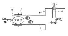
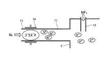
図1に示すように、真空処理装置(エッチング装置)1には真空排気系に接続される仕込取出槽2が備えられ、仕込取出槽2の上方には真空処理槽3が備えられている(処理設備)。仕込取出槽2の内部には所定速度で回転可能なターンテーブル4が設けられ、ターンテーブル4には基板としてのシリコン基板5を保持するボート6が支持される。ボート6にはシリコン基板5が複数枚(例えば、50枚)収容され、複数枚のシリコン基板5は所定間隔で互いに平行に配されている。 As shown in FIG. 1, the vacuum processing apparatus (etching apparatus) 1 is provided with a charging / discharging
シリコン基板5のシリコンは、単結晶シリコン、多結晶シリコン(ポリシリコン)の何れであってもよく、以下には、単にシリコンと称してある。このため、ポリシリコンのシリコン基板を適用した場合、後述するシリコン層のエッチングは、ポリシリコン層のエッチングとなる。 The silicon of the
仕込取出槽2の上部には鉛直方向に伸びる送りねじ7が設けられ、送りねじ7の駆動によりターンテーブル4が昇降動作する。仕込取出槽2と真空処理槽3は連通口8を介して内部が連通し、シャッタ手段9により雰囲気的に隔離されるようになっている。シャッタ手段9の開閉及びターンテーブル4の昇降により、仕込取出槽2と真空処理槽3の間でボート6(シリコン基板5)の受け渡しが行われる。 A
尚、図中の符号で10は、真空処理槽3の内部の真空排気を行う排出部である。 Note that
真空処理槽3の側部にはラジカル状態の水素(Hラジカル:H*)が導入される第1導入口11が2箇所に設けられ、真空処理槽3の内部には第2処理ガス(処理ガス)としてのNF3が導入されるシャワーノズル12が設けられている。2箇所の第1導入口11から導入されるHラジカルH*とシャワーノズル12から導入されるNF3が反応することにより、真空処理槽3の内部に前駆体NHxFyが生成される。In the side portion of the
図2に示すように、第1導入口11には第1導入路13が接続され、第1導入路13にはプラズマ発生部14が設けられている。プラズマ発生部14はマイクロ波により処理ガスをプラズマ状態にするものである。第1導入路13には流量調整手段15を介して第1処理ガスとしてのNH3ガス(NH3ガスまたはH2ガスの少なくともいずれか一方)及びN2ガスが供給され、プラズマ発生部14でNH3ガス及びN2ガスがプラズマ状態にされることによりHラジカルH*が生成される。シャワーノズル12には流量調整手段16を介してNF3ガスが供給される。As shown in FIG. 2, a
第1導入口11、第1導入路13及び流量調整手段15により第1処理ガス導入手段が構成され、シャワーノズル12、流量調整手段16により第2処理ガス導入手段が構成されている。 The first process gas introduction means is constituted by the
真空処理槽3には温度制御手段としての図示しないランプヒータが設けられ、ランプヒータにより真空処理槽3の内部の温度、即ち、シリコン基板5の温度が所定状態に制御される。流量調整手段15、16による処理ガスの流通状況、及び、ランプヒータの動作状態は制御手段としての図示しない制御装置により適宜制御される。 The
上述した真空処理装置1では、シリコン基板5を保持したボート6が真空処理槽3の内部に搬入され、真空処理槽3の内部を気密状態にして所定の圧力になるように真空排気が行われる。 In the above-described
制御装置からの指令により、ラジカル状態のNH3ガスとN2ガス、NF3ガスを真空処理槽3に導入し、所定の真空状態の雰囲気に配置されたシリコン基板5の自然酸化膜表面(SiO2)と処理ガスとを反応(低温での吸着反応)させることで、反応生成物(Fy及びNHxの化合物{(NH4)2SiF6})を生成する。そして、ランプヒータを動作させてシリコン基板5を所定温度に制御することにより(高温にすることにより)、反応生成物{(NH4)2SiF6}を昇華させてシリコン基板5の表面の自然酸化膜を除去(エッチング)する。In accordance with a command from the control device, radical NH3 gas, N2 gas, and NF3 gas are introduced into the
自然酸化膜が除去されたシリコン基板5の配置を維持した状態で、制御装置からの指令により、補助処理ガスとしてラジカル状態のNH3ガス及びN2ガス、NF3ガスを真空処理槽3に導入する。即ち、自然酸化膜をエッチングする際の処理ガスと同一の処理ガスを導入する。真空処理槽3に生成されたラジカル状態のF(Fラジカル:F*)をシリコン基板5の表面に作用させ、所定厚のシリコン層をエッチングする。In a state where the arrangement of the
この時、NHxFyがFラジカル:F*と共に真空処理槽3に存在するが、NHxFyは高温雰囲気ではシリコン基板5の表面には作用しない。このため、制御装置によりランプヒータの動作が制御されることにより、自然酸化膜をエッチングした際の所定温度(例えば、100℃〜400℃)の状態がシリコン層をエッチングする際にも維持され、自然酸化膜がエッチングされた後は、Fラジカル:F*だけをシリコン基板5の表面に作用させて所定厚のシリコン層をエッチングすることができる。At this time, NHxFy exists in the
更に、所定厚のシリコン層がエッチングされたシリコン基板5の配置を維持した状態で、処理ガスNH3ガスとN2ガス、NF3ガスを真空処理槽3に導入し、所定の真空状態の雰囲気に配置されたシリコン基板5の副生成物(SiOF、SiOH)と処理ガスに基づくフッ化アンモニウム(NH4F)とを反応(低温での吸着反応)させ、反応副生成物Fy及びNHxの化合物{(NH4)2SiF6}を生成する。そして、ランプヒータを動作させてシリコン基板5を所定温度に制御することにより(高温にすることにより)、反応副生成物{(NH4)2SiF6}を昇華させてシリコン基板5の表面の副生成物を除去(エッチング)する。Further, in a state where the arrangement of the
尚、副生成物(SiOF、SiOH)を除去するに際し、フッ化アンモニウムを生成するために、NF3ガス及びラジカル状態のNH3ガスとN2ガスを導入した例を挙げているが、NF3ガス及びラジカル状態のH2ガスとN2ガスを導入することも可能である。また、HFガスとNF3ガスを導入することが可能である。Incidentally, by-products (SiOF, SiOH) upon removing, in order to produce ammonium fluoride, although an example of introducing NF3 gas and NH3 gas andN 2 gas in the radical state, NF3 It is also possible to introduce gas and radical H2 gas and N2 gas. It is also possible to introduce HF gas and NF3 gas.
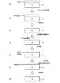
図3〜図5に基づいて自然酸化膜のエッチングを説明する。 The etching of the natural oxide film will be described with reference to FIGS.
図3に示すように、第1導入路13からNH3ガス(NH3ガスまたはH2ガスの少なくともいずれか一方)及びN2ガスを導入し、プラズマ発生部でHラジカルH*を生成し、第1導入口11からHラジカルH*を真空処理槽3に導入する。同時に、シャワーノズル12からNF3ガスを真空処理槽3に導入し、HラジカルH*とNF3ガスを混合させて反応させてNHxFyを生成させる。
即ち、
H*+NF3→NHxFy(NH4FH、NH4FHF等)As shown in FIG. 3, NH3 gas (at least one of NH3 gas and H2 gas) and N2 gas are introduced from the
That is,
H* + NF3 → NHxFy (NH4 FH, NH4 FHF, etc.)
図4(a)に示すように、NHxFyとシリコン基板5の自然酸化表面(SiO2)が反応し、図4(b)に示すように、Fy及びNHxの化合物である(NH4)2SiF6が生成される。
即ち、
NHxFy+SiO2→(NH4)2SiF6+H2O↑As shown in FIG. 4 (a), NHxFy reacts with the naturally oxidized surface (SiO2 ) of the
That is,
NHxFy + SiO2 → (NH4 )2 SiF6 + H2 O ↑
その後、ランプヒータにより真空処理槽3を加熱し(例えば、100℃〜400℃)、図4(c)に示すように、(NH4)2SiF6を分解して昇華させ、シリコン基板5の表面から除去する。
即ち、
(NH4)2SiF6→NH3↑+HF↑+SiF4↑Thereafter, the
That is,
(NH4 )2 SiF6 → NH3 ↑ + HF ↑ + SiF4 ↑
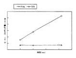
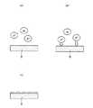
シリコン基板5の表面をエッチングして(NH4)2SiF6を除去することで、図4(d)に示すように、シリコン基板5の表面の自然酸化膜が除去され、清浄な表面とされる。この時、図5に○印で示すように、自然酸化膜はエッチング時間に応じてエッチング量が増加し、図5に□印で示すように、シリコン層はエッチング時間が長くなってもエッチング量はほとんど変化がなく、シリコン層はエッチングされていないことが判る。By etching the surface of the
自然酸化膜が除去されたシリコン基板5の配置を維持した状態で、即ち、同一の真空処理槽3で、自然酸化膜が除去されたシリコン基板5の表面(シリコン層)をエッチングする。これにより、酸化膜の界面とされたシリコン面の酸素、例えば、シリコンの金属格子間等に存在する虞のある酸素が除去され、表面から酸素が確実に除去されたシリコン基板5を得ることができる。しかも、自然酸化膜をエッチングする装置でシリコン層をエッチングするため、搬送による酸化等が生じることがなく、極めて簡単な処理で高い表面清浄度を有するシリコン基板5を得ることができる。 In a state where the arrangement of the
図6〜図8に基づいて自然酸化膜が除去された後のシリコン層のエッチングを説明する。 The etching of the silicon layer after the natural oxide film is removed will be described with reference to FIGS.
図6に示すように、第1導入路13からNH3ガス(NH3ガスまたはH2ガスの少なくともいずれか一方)及びN2ガスを導入し、プラズマ発生部14でHラジカルH*及びNラジカルN*を生成し、第1導入口11からHラジカルH*及びNラジカルN*を真空処理槽3に導入する。同時に、シャワーノズル12からNF3ガスを真空処理槽3に導入し、HラジカルH*とNF3ガスを混合させて反応させて前駆体NHxFyを生成させると共に、NラジカルN*とNF3ガスを混合させて反応させてFラジカルF*を生成させる。
即ち、
H*+NF3→NHxFy(NH4FH、NH4FHF等)
N*+NF3→N2+F2+F*(3F*等)As shown in FIG. 6, NH3 gas (at least one of NH3 gas and H2 gas) and N2 gas are introduced from the
That is,
H* + NF3 → NHxFy (NH4 FH, NH4 FHF, etc.)
N* + NF3 → N2 + F2 + F* (3F* etc.)
図7(a)に示すように、真空処理槽3の内部は、自然酸化膜を除去、即ち、(NH4)2SiF6を分解・昇華するために加熱雰囲気に維持されている。このため、前駆体NHxFyは高温に維持されたシリコン基板5の表面(シリコン面)と反応せず、図7(b)に示すように、FラジカルF*がシリコン基板5の表面に作用して表面がエッチングされる。
即ち、
Si+4F*→SiF4↑As shown in FIG. 7A, the inside of the
That is,
Si + 4F* → SiF4 ↑
これにより、図7(c)に示すように、自然酸化膜の界面とされたシリコン面の酸素が除去され、表面から酸素が確実に除去されたシリコン基板5を得ることができる。この時、図8に□印で示すように、シリコン層はエッチング時間に応じてエッチング量が増加し、図8に△印で示すように、シリコン層以外の層(例えば、SiN)はエッチング時間が長くなってもエッチング量はほとんど変化がなく、シリコン層だけがエッチングされることが判る。 As a result, as shown in FIG. 7C, oxygen on the silicon surface which is the interface of the natural oxide film is removed, and the
FラジカルF*をシリコン基板5の表面に作用させて表面をエッチングした場合、シリコン基板5の表面に副生成物(SiOF、SiOH)が生成されることが考えられる。このため、シリコン基板5の配置を維持した状態で、即ち、同一の真空処理槽3で、所定厚のシリコン層がエッチングされたシリコン基板5の表面の副生成物(SiOF、SiOH)を除去する。このため、自然酸化膜を除去する処理装置を用い、酸素除去で生じる虞のある副生成物を含めてシリコン基板5の表面の酸素を確実に除去することができる。When the surface is etched by causing the F radical F* to act on the surface of the
図3及び図9に基づいて、所定厚のシリコン層がエッチングされたシリコン基板5の表面の副生成物(SiOF、SiOH)を除去する状況を説明する。 Based on FIGS. 3 and 9, a situation in which by-products (SiOF, SiOH) on the surface of the
処理ガスの導入は自然酸化膜を除去する時(図3)と同一である。図3に示すように、第1導入路13からNH3ガス(NH3ガスまたはH2ガスの少なくともいずれか一方)及びN2ガスを導入し、プラズマ発生部でHラジカルH*を生成し、第1導入口11からHラジカルH*を真空処理槽3に導入する。同時に、シャワーノズル12からNF3ガスを真空処理槽3に導入し、HラジカルH*とNF3ガスを混合させて反応させてNHxFyを生成させる。
即ち、
H*+NF3→NHxFy(NH4FH、NH4FHF等)The introduction of the processing gas is the same as when the natural oxide film is removed (FIG. 3). As shown in FIG. 3, NH3 gas (at least one of NH3 gas and H2 gas) and N2 gas are introduced from the
That is,
H* + NF3 → NHxFy (NH4 FH, NH4 FHF, etc.)
図9(a)に示すように、NHxFyとシリコン基板5の表面の副生成物(SiOF、SiOH)が反応し、図9(b)に示すように、Fy及びNHxの化合物である(NH4)2SiF6が生成される。
即ち、
NHxFy+SiOF(SiOH)→(NH4)2SiF6+H2O↑As shown in FIG. 9A, NHxFy and by-products (SiOF, SiOH) on the surface of the
That is,
NHxFy + SiOF (SiOH) → (NH4 )2 SiF6 + H2 O ↑
その後、ランプヒータにより真空処理槽3を加熱し(例えば、100℃〜400℃)、図9(c)に示すように、(NH4)2SiF6を分解して昇華させ、シリコン基板5の表面から除去する。
即ち、
(NH4)2SiF6→NH3↑+HF↑+SiF4↑Thereafter, the
That is,
(NH4 )2 SiF6 → NH3 ↑ + HF ↑ + SiF4 ↑
シリコン基板5の表面をエッチングして(NH4)2SiF6を除去することで、図9(d)に示すように、シリコン基板5の表面の自然酸化膜が除去され、副生成物(SiOF、SiOH)を含む酸素が除去された極めて清浄な表面とされる。By etching the surface of the
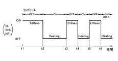
上述した自然酸化膜のエッチング及びシリコン層のエッチング、副生成物のエッチングにおける処理ガス{NH3ガス(NH3ガスまたはH2ガスの少なくともいずれか一方)及びN2ガス、NF3ガス}の導入状況を図10に基づいて説明する。その時の一連の工程の状況を図11に示してある。Introduction of the processing gas {NH3 gas (at least one of NH3 gas or H2 gas), N2 gas, NF3 gas} in the etching of the natural oxide film, the silicon layer, and the by-product described above The situation will be described with reference to FIG. The status of a series of steps at that time is shown in FIG.
時間t1から時間t2の間(例えば、520sec)は処理ガスが導入(ON)され、ランプヒータがOFFにされ、前駆体NHxFyが自然酸化膜SiO2と反応する処理が実施される(図4(a)(b)、図11(a)(b)参照)。時間t2から時間t3の間は処理ガスが停止(OFF)され、ランプヒータがONにされ、化合物である(NH4)2SiF6が分解して昇華され自然酸化膜SiO2がエッチングされる(図4(c)(d)、図11(c)参照)。Between time t1 and time t2 (for example, 520 sec), the processing gas is introduced (ON), the lamp heater is turned off, and the process in which the precursor NHxFy reacts with the natural oxide film SiO2 is performed (FIG. 4 ( a) (b), see FIG. 11 (a) (b)). From time t2 to time t3, the processing gas is stopped (OFF), the lamp heater is turned on, the compound (NH4 )2 SiF6 is decomposed and sublimated, and the natural oxide film SiO2 is etched ( 4 (c) (d) and FIG. 11 (c)).
続いて、時間t3から時間t4の間(例えば、50〜210sec)は再び処理ガスが導入(ON)され、ランプヒータがOFFにされ、FラジカルF*を生成させる。加熱雰囲気に保たれ、時間t4から時間t5の間、ランプヒータがONされ、FラジカルF*によりシリコン層がエッチングされる(図7(a)(b)(c)、図11(d)参照)。Subsequently, the processing gas is again introduced (ON) from time t3 to time t4 (for example, 50 to 210 seconds), the lamp heater is turned off, and F radical F* is generated. In a heated atmosphere, the lamp heater is turned on from time t4 to time t5, and the silicon layer is etched by F radicals F* (see FIGS. 7A, 7B, and 11C). ).
更に、時間t5から時間t6の間(例えば、50〜210sec)は処理ガスが導入(ON)され、適宜ランプヒータがOFFされ、前駆体NHxFyが副生成物(SiOF、SiOH)と反応する処理が実施される(図9(a)(b)、図11(e)(f)参照)。時間t6以降は処理ガスが停止(OFF)され、温度が維持されるようにランプヒータがON・OFFされ、化合物である(NH4)2SiF6が分解して昇華され副生成物(SiOF、SiOH)がエッチングされる(図9(c)(d)、図11(g)参照)。Further, during the period from time t5 to time t6 (for example, 50 to 210 sec), the processing gas is introduced (ON), the lamp heater is appropriately turned off, and the process in which the precursor NHxFy reacts with the by-products (SiOF, SiOH) is performed. (See FIGS. 9 (a) and 9 (b) and FIGS. 11 (e) and 11 (f)). After time t6, the processing gas is stopped (OFF), the lamp heater is turned ON / OFF so that the temperature is maintained, and the compound (NH4 )2 SiF6 is decomposed and sublimated to produce by-products (SiOF, SiOH) is etched (see FIGS. 9C, 9D, and 11G).
尚、時間t3、時間t5の時点で処理槽内を冷却するクーリング工程を実施することも可能である。 In addition, it is also possible to implement the cooling process which cools the inside of a processing tank at the time t3 and the time t5.
上述したように、第1実施形態例では、同一の真空処理槽3の内部で、自然酸化膜の除去と自然酸化膜が除去されたシリコン層の除去、及びシリコン層の除去で生成される副生成物の除去が行える。このため、自然酸化膜を除去する真空処理装置1を用い、簡単な制御で短時間に、自然酸化膜が除去された後にシリコン基板5の界面の酸素を確実に除去することができ、しかも、酸素除去で生じる虞のある副生成物を含めて除去することができる。従って、簡単な真空処理装置1及び処理方法により、極めて性能が高い表面を有するシリコン基板5を得ることが可能になる。 As described above, in the first embodiment, in the same
上述した自然酸化膜の除去と自然酸化膜が除去されたシリコン層の除去は、図12に示すように、半導体基板のコンタクトホールCの底面の清浄処理に用いられる。即ち、コンタクトホールCの自然酸化膜が(NH4)2SiF6の昇華により除去され、その後、連続してシリコン層が除去される。更に、シリコン層の除去の際に生成される副生成物(SiOF、SiOH)が(NH4)2SiF6の昇華により除去される。これにより、副生成物を含めて酸素が確実に除去された底面を有するコンタクトホールCを形成することができ、その後、配線用の金属を積層した際に抵抗が極めて少ない配線を実現することができる。The above-described removal of the natural oxide film and the removal of the silicon layer from which the natural oxide film has been removed are used for cleaning the bottom surface of the contact hole C of the semiconductor substrate, as shown in FIG. That is, the natural oxide film in the contact hole C is removed by sublimation of (NH4 )2 SiF6 , and then the silicon layer is continuously removed. Further, by-products (SiOF, SiOH) generated when the silicon layer is removed are removed by sublimation of (NH4 )2 SiF6 . This makes it possible to form a contact hole C having a bottom surface from which oxygen is surely removed, including by-products, and then to realize a wiring with extremely low resistance when a wiring metal is laminated. it can.
図13、図14に基づいて自然酸化膜が除去された後のシリコン層のエッチング方法(真空処理方法)の第2実施形態例を説明する。図13には本発明の第2実施形態例におけるシリコン層を除去する際の処理ガスの状況を表す概念、図14には本発明の第2実施形態例におけるシリコン層除去の工程説明を示してある。尚、真空処理装置1の構成は第1実施形態例と同一であるので構成の説明は省略してある。 A second embodiment of the silicon layer etching method (vacuum processing method) after the natural oxide film is removed will be described with reference to FIGS. FIG. 13 shows a concept representing the state of the processing gas when removing the silicon layer in the second embodiment of the present invention, and FIG. 14 shows the process of removing the silicon layer in the second embodiment of the present invention. is there. Since the configuration of the
第2実施形態例に係るエッチング方法は、自然酸化膜を除去する場合、第1処理ガス、第2処理ガス(処理ガス)としてNH3ガス(NH3ガスまたはH2ガスの少なくともいずれか一方)、N2ガス及びNF3ガスを用い、シリコン層を除去する場合、補助処理ガスとしてNH3ガスを停止し、N2とNF3を用いる。つまり、シリコン層を除去する場合、真空処理装置1の内部に前駆体NHxFyを生成させずにFラジカルF*をシリコン基板5に作用させる。このため、以下にはシリコン層の除去について説明してある。In the etching method according to the second embodiment, when the natural oxide film is removed, NH3 gas (at least one of NH3 gas and H2 gas) is used as the first processing gas and the second processing gas (processing gas). When removing the silicon layer using N2 gas and NF3 gas, NH3 gas is stopped as auxiliary process gas, and N2 and NF3 are used. That is, when removing the silicon layer, the F radical F* is allowed to act on the
図13に示すように、第1導入路13からN2ガスを導入し{NH3ガス(NH3ガスまたはH2ガスの少なくともいずれか一方)を停止し}、プラズマ発生部14でNラジカルN*を生成し、第1導入口11からNラジカルN*を真空処理槽3に導入する。同時に、シャワーノズル12からNF3ガスを真空処理槽3に導入し、NラジカルN*とNF3ガスを混合させて反応させてFラジカルF*を生成させる。
即ち、
N*+NF3→N2+F2+F*(3F*等)As shown in FIG. 13, N2 gas is introduced from the first introduction path 13 {NH3 gas (at least one of NH3 gas and H2 gas) is stopped}, and N radical N is generated in the
That is,
N* + NF3 → N2 + F2 + F* (3F* etc.)
図14(a)に示すように、真空処理槽3の内部にFラジカルF*が導入され、図14(b)に示すように、FラジカルF*がシリコン基板5の表面に作用して表面がエッチングされる。
即ち、
Si+4F*→SiF4↑As shown in FIG. 14 (a), F radicals F* are introduced into the inside of the
That is,
Si + 4F* → SiF4 ↑
これにより、図14(c)に示すように、自然酸化膜の界面とされたシリコン面の酸素が除去され、表面から酸素が確実に除去されたシリコン基板5を得ることができる。また、NH3ガス(NH3ガスまたはH2ガスの少なくともいずれか一方)を停止しているので、前駆体NHxFyが生成されず、比較的低温の場合でもFラジカルF*をシリコン基板5の表面に作用させることができ、短時間でシリコン層のエッチングを行うことができる。As a result, as shown in FIG. 14C, the
上述したように、第2実施形態例では、第1実施形態例と同様に、同一の真空処理槽3の内部で、自然酸化膜の除去と自然酸化膜が除去されたシリコン層の除去が行え、簡単な制御で短時間に、自然酸化膜が除去された後にシリコン基板5の界面の酸素を確実に除去することができる。従って、簡単な真空処理装置1及び処理方法により、極めて性能が高い表面を有するシリコン基板5を得ることが可能になる。 As described above, in the second embodiment, as in the first embodiment, the natural oxide film and the silicon layer from which the natural oxide film has been removed can be removed within the same
尚、上述した各実施形態例では、シリコン層のエッチングの際、NH3ガス(NH3ガスまたはH2ガスの少なくともいずれか一方)及びN2ガスとNF3ガスを別々のガス導入手段から導入しているが、これに限らず、プラズマ発生部を有する同一のガス導入手段からすべてのガスを導入してもよい。この場合には、NF3ガスに直接プラズマを印加してFラジカルを作成することができる。In each of the embodiments described above, when etching the silicon layer, NH3 gas (at least one of NH3 gas and H2 gas), N2 gas and NF3 gas are introduced from separate gas introduction means. However, the present invention is not limited to this, and all gases may be introduced from the same gas introduction means having a plasma generation unit. In this case, F radicals can be created by directly applying plasma to NF3 gas.
図15に基づいてバッチ処理を行う装置の他の例を説明する。図15には本発明の他の実施形態例に係る真空処理装置の概略を表す全体構成を示してある。 Another example of an apparatus that performs batch processing will be described with reference to FIG. FIG. 15 shows an overall configuration representing an outline of a vacuum processing apparatus according to another embodiment of the present invention.
処理設備である真空処理室21(エッチング室)にはプラズマ状態の処理ガス及びNF3が導入され、真空処理室21の上部にはバルブ22を介して処理設備である冷却室23が備えられている。冷却室23には不活性ガス(N2ガス)が導入されて室内が冷却される。真空処理室21及び冷却室23は真空系24、25により所定の真空状態にされる。真空処理室21にはヒータ26が設けられ、ヒータ26により真空処理室21の内部が所望の温度に制御される。A processing gas in a plasma state and NF3 are introduced into a vacuum processing chamber 21 (etching chamber) that is a processing facility, and a
真空処理室21には昇降機構27が備えられ、ボート6に保持された複数のシリコン基板5が昇降される。バルブ22の開閉及び昇降機構27を連動することで、真空処理室21と冷却室23の間で複数のシリコン基板5を移動させることができる。冷却室23はバルブ22を介して図示しないロードロック室と接続され、バルブ22の開閉によりボート6に保持された複数のシリコン基板5が移送(搬入・搬出)される。 The
上述した真空処理装置1では、シリコン基板5に対する自然酸化膜の除去及びシリコン層の除去、副生成物の除去が真空処理室21で実施される。また、温度制御を行う場合の冷却は冷却室23で実施される。例えば、前述した一連の工程の中で、図10に示した時間t3、時間t5の時点で処理槽内を冷却する場合のクーリング工程を行う場合、バルブ22の開閉及び昇降機構27を連動させ、ボート6に保持された複数のシリコン基板5を昇降させて冷却室23で冷却が実施される。 In the
冷却室23を備えたことにより、一連の工程の中で、自然酸化膜の除去及びシリコン層の除去、副生成物の除去を行う場合の温度制御を短時間に行うことができ、生産性を向上させることができる。 By providing the cooling
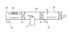
本発明は、処理室内に基板を一枚づつ配する、いわゆる、枚葉式の装置で処理を行うことも可能である。図16から図18に基づいて枚葉式の装置の例を説明する。図16には本発明の他の実施形態例に係る真空処理装置の概略を表す全体構成、図17、図18には図16中のA−A線矢視、B−B線矢視を示してある。 In the present invention, processing can be performed by a so-called single-wafer type apparatus in which substrates are disposed one by one in a processing chamber. An example of a single wafer type apparatus will be described with reference to FIGS. FIG. 16 shows an overall configuration representing an outline of a vacuum processing apparatus according to another embodiment of the present invention, and FIGS. 17 and 18 show an AA arrow view and a BB arrow view in FIG. It is.
図に示すように、搬送ロボット31を備えた搬送室42が備えられ、搬送室42の周囲にはバルブ41を介してロードロック室32、真空処理室(エッチング室)33、加熱室35、冷却室34が配されている。真空処理室33にはプラズマ状態の処理ガス及びNF3が導入され、加熱室35にはヒータ36が備えられている。また、冷却室34には不活性ガス(N2ガス)が導入されて室内が冷却される。As shown in the figure, a
処理前のシリコン基板はロードロック室32に搬入され、処理が終了したシリコン基板はロードロック室32から搬出される。搬送ロボット31の動作及びバルブ41の開閉が連動して制御され、シリコン基板は、真空処理室33、加熱室35、冷却室34に適宜搬送され、真空処理室33、加熱室35、冷却室34から適宜搬出される。複数の処理室内にシリコン基板を一枚づつ配した状態で所定の処理が施される。 The silicon substrate before processing is carried into the
上述した真空処理装置では、シリコン基板に対する自然酸化膜の除去及びシリコン層の除去、副生成物の除去が真空処理室33で実施される。また、温度制御を行う場合の加熱は加熱室35で実施され、温度制御を行う場合の冷却は冷却室34で実施される。シリコン層を除去する場合、FラジカルF*が生成されるため、シリコン層の除去を実施するための真空処理室33を追加することも可能である。In the vacuum processing apparatus described above, removal of the natural oxide film, removal of the silicon layer, and removal of by-products from the silicon substrate are performed in the
複数の処理室を備え、各処理室でシリコン基板を1枚づつ処理するので、一連の工程の中で、自然酸化膜の除去及びシリコン層の除去、副生成物の除去を行う場合、均一に処理を行うことができ、高い性能の製品を得ることができる。 A plurality of processing chambers are provided, and silicon substrates are processed one by one in each processing chamber. Therefore, when removing a natural oxide film, a silicon layer, and a by-product in a series of steps, it is uniform. Processing can be performed and a product with high performance can be obtained.
上述した実施形態では、自然酸化膜と副生成物を除去する場合に同一のガスを用いた場合を記載したが、異なるガスを用いてもよく、例えば、副生成物を除去するガスとして、無水フッ化水素酸ガス(AHF)とN2ガスとエタノール(C2H5OH)又はメタノール(CH3OH)で飽和されたN2ガスを用いてもよい。In the above-described embodiment, the case where the same gas is used to remove the natural oxide film and the by-product has been described. However, different gases may be used, for example, anhydrous gas as a gas for removing the by-product. it may be used hydrofluoric acid gas (AHF) andN 2 gas and ethanol(C2 H 5 OH) or
この場合には、マスフローコントローラーを通じて無水フッ化水素酸ガス(AHF)とN2ガスを同一の配管から真空処理室に導入し、別の配管から容器内のエタノール(C2H5OH)又はメタノール(CH3OH)をバブリングすることによりエタノール(C2H5OH)又はメタノール(CH3OH)で飽和されたN2ガスを導入する。In this case, anhydrous hydrofluoric acid gas (AHF) and N2 gas are introduced into the vacuum processing chamber from the same pipe through a mass flow controller, and ethanol (C2 H5 OH) or methanol in the container is sent from another pipe.(CH 3 OH) are introduced ethanol(C2 H 5 OH) or
真空処理室内では、無水フッ化水素酸ガス(AHF)とエタノール(C2H5OH)又はメタノール(CH3OH)で飽和されたN2ガスとの反応により、シリコン基板表面の副生成物(例えば、SiOF)を除去することができる。In the vacuum processing chamber, a by-product on the surface of the silicon substrate (AHF) is reacted with N2 gas saturated with ethanol (C2 H5 OH) or methanol (CH3 OH). For example, SiOF) can be removed.
具体的には、無水フッ化水素酸ガス(AHF)とエタノールエタノール(C2H5OH)又はメタノール(CH3OH)との反応により、HF2−が生成される。
即ち、
C2H5OH+2HF→C2H5OH2++HF2−
CH3OH+2HF→CH3OH2++HF2−Specifically, HF2− is generated by a reaction between anhydrous hydrofluoric acid gas (AHF) and ethanol ethanol (C2 H5 OH) or methanol (CH3 OH).
That is,
C2 H5 OH + 2HF → C2 H5 OH2+ + HF2−
CH3 OH + 2HF → CH3 OH2+ + HF2−
生成されたHF2−は副生成物(例えば、SiOF)のエッチングに寄与する。副生成物のエッチングで生じたSiF4とH2Oはエタノール(C2H5OH)やメタノール(CH3OH)との親和性がよく、過剰の(C2H5OH)やメタノール(CH3OH)蒸気と共に排気される。The generated HF2− contributes to the etching of by-products (eg, SiOF). SiF4 and H2 O generated by etching of the by-product have good affinity with ethanol (C2 H5 OH) and methanol (CH3 OH), and excess (C2 H5 OH) and methanol (CH3 OH) exhausted with steam.
また、上述した実施形態では、副生成物の除去をガスを用いたいわゆるドライエッチングを用いた場合を記載したが、これに限られず、ウエットエッチング法を用いて副生成物の除去を行ってもよい。この場合には、例えば、シリコン層を除去した後、シリコン基板を別の処理室に搬送し、フッ化水素(HF)で満たされた容器内に基板を浸すことにより行う。この処理により、シリコン基板表面の副生成物(例えば、SiOF)を除去することができる。 Further, in the above-described embodiment, the case where so-called dry etching using a gas is used for removing the by-product is described. However, the present invention is not limited to this, and even if the by-product is removed using a wet etching method. Good. In this case, for example, after removing the silicon layer, the silicon substrate is transferred to another processing chamber, and the substrate is immersed in a container filled with hydrogen fluoride (HF). By this treatment, a byproduct (for example, SiOF) on the surface of the silicon substrate can be removed.
本発明は、真空状態の処理設備でエッチングを行う真空処理方法及び真空処理装置の産業分野で利用することができる。 INDUSTRIAL APPLICATION This invention can be utilized in the industrial field | area of the vacuum processing method and vacuum processing apparatus which etch with the processing equipment of a vacuum state.
1 真空処理装置
2 仕込取出槽
3 真空処理槽
4 ターンテーブル
5 シリコン基板
6 ボート
7 送りねじ
8 連通口
9 シャッタ手段
10 排出部
11 第1導入口
12 シャワーノズル
13 第1導入路
14 プラズマ発生部
15、16 流量調整手段DESCRIPTION OF
Claims (17)
Translated fromJapanese酸化膜が除去された前記シリコン基板の配置を維持した状態で、補助処理ガスを導入して前記シリコン基板の表面にFラジカルを作用させ所定厚のシリコン層を除去し、
シリコン層を除去した後、前記シリコン層の除去の際に生成されたシリコン基板の表面の副生成物を除去する
ことを特徴とする真空処理方法。Introducing a processing gas, reacting with an oxidized surface of a silicon substrate placed in a predetermined vacuum atmosphere, generating a reaction product, and sublimating the reaction product by controlling the silicon substrate to a predetermined temperature. Remove the oxide film on the surface of the silicon substrate,
In a state where the arrangement of the silicon substrate from which the oxide film has been removed is maintained, an auxiliary processing gas is introduced to cause F radicals to act on the surface of the silicon substrate to remove a silicon layer having a predetermined thickness,
After removing the silicon layer, a by-product on the surface of the silicon substrate generated during the removal of the silicon layer is removed.
前記処理ガスを導入し、前記シリコン層が除去された前記シリコン基板の表面の副生成物と反応させて反応副生成物を生成し、シリコン基板を所定温度に制御することにより前記反応副生成物を昇華させてシリコン基板の表面の副生成物を除去する
ことを特徴とする真空処理方法。The vacuum processing method according to claim 1,
Introducing the processing gas, reacting with a by-product on the surface of the silicon substrate from which the silicon layer has been removed to produce a reaction by-product, and controlling the silicon substrate to a predetermined temperature to thereby produce the reaction by-product A vacuum processing method characterized in that byproducts on the surface of the silicon substrate are removed by sublimating the substrate.
シリコン層が除去された前記シリコン基板の配置を維持した状態で、前記シリコン基板の表面の副生成物を除去する
ことを特徴とする真空処理方法。In the vacuum processing method of Claim 2,
A vacuum processing method, wherein a by-product on the surface of the silicon substrate is removed while maintaining the arrangement of the silicon substrate from which the silicon layer has been removed.
前記処理ガスはNH3またはH2の少なくともいずれか一方とN2及びNF3であり、
前記反応生成物及び前記反応副生成物を100℃〜400℃の雰囲気で昇華させ、
前記補助処理ガスとして前記処理ガス、もしくは、N2とNF3を導入して前記シリコン基板の表面にFラジカルを作用させる
ことを特徴とする真空処理方法。In the vacuum processing method of Claim 2 or Claim 3,
The processing gas is at least one of NH3 and H2 and N2 and NF3 ,
Sublimating the reaction product and the reaction by-product in an atmosphere of 100 ° C. to 400 ° C .;
A vacuum processing method, wherein the processing gas or N2 and NF3 are introduced as the auxiliary processing gas to cause F radicals to act on the surface of the silicon substrate.
前記補助処理ガスを同一のガス導入手段から導入する
ことを特徴とする真空処理方法。In the vacuum processing method of Claim 4,
A vacuum processing method, wherein the auxiliary processing gas is introduced from the same gas introduction means.
無水フッ化水素酸ガス(AHF)とN2ガスとエタノール(C2H5OH)又はメタノール(CH3OH)で飽和されたN2ガスを用いて、前記シリコン基板表面の前記副生成物を除去する
ことを特徴とする真空処理方法。The vacuum processing method according to claim 1,
With anhydrous hydrofluoric acid gas (AHF) andN 2 gas and ethanol(C2 H 5 OH) or methanol(CH 3 OH) saturated withN 2 gas, the by-products of the silicon substrate surface The vacuum processing method characterized by removing.
前記シリコン層を除去した後、ウエットエッチング法を用いて、前記シリコン基板表面の前記副生成物を除去する
こと特徴とする真空処理方法。The vacuum processing method according to claim 1,
After removing the silicon layer, the by-product on the surface of the silicon substrate is removed using a wet etching method.
ウエットエッチング法の溶液として、フッ化水素(HF)を用いる
ことを特徴とする真空処理方法。In the vacuum processing method of Claim 7,
A vacuum processing method characterized by using hydrogen fluoride (HF) as a solution of a wet etching method.
前記副生成物がSiOFである
ことを特徴とする真空処理方法。In the vacuum processing method according to any one of claims 1 to 8,
The vacuum treatment method, wherein the by-product is SiOF.
シリコン基板を所定温度に制御することにより前記反応生成物を昇華させてシリコン基板の表面の酸化膜を除去し、酸化膜が除去された前記シリコン基板の配置を維持した状態で、補助処理ガスとして、前記処理ガス、もしくは、N2とNF3を、前記処理ガスと同一のガス導入手段から導入して前記シリコン基板の表面にFラジカルを作用させ所定厚のシリコン層を除去した後、
前記シリコン基板の配置を維持した状態で、前記シリコン層の除去の際に生成されたシリコン基板の表面の副生成物を、シリコン基板を100℃〜400℃に制御することにより除去する
ことを特徴とする真空処理方法。As a processing gas, at least one of NH3 and H2 and N2 and NF3 are introduced and reacted with an oxidized surface of a silicon substrate placed in a predetermined vacuum atmosphere to generate a reaction product,
As an auxiliary process gas, the reaction product is sublimated by controlling the silicon substrate to a predetermined temperature to remove the oxide film on the surface of the silicon substrate, and the arrangement of the silicon substrate from which the oxide film has been removed is maintained. After introducing the processing gas, or N2 and NF3 from the same gas introducing means as the processing gas, F radicals act on the surface of the silicon substrate to remove the silicon layer having a predetermined thickness,
The by-product on the surface of the silicon substrate generated during the removal of the silicon layer is removed by controlling the silicon substrate at 100 ° C. to 400 ° C. while maintaining the arrangement of the silicon substrate. A vacuum processing method.
第1処理ガスまたは補助処理ガスを前記処理設備内に導入する第1処理ガス導入手段と、
前記第1処理ガスまたは補助処理ガスと反応する第2処理ガスを前記処理設備内に導入する第2処理ガス導入手段と、
前記処理設備内を所定の温度に制御することで、前記第1処理ガスと前記第2処理ガスと前記基板表面の自然酸化膜とを反応させる一方、前記第1処理ガスと前記第2処理ガスと前記基板表面の副生成物とを反応させる温度制御手段と、
前記第1処理ガス導入手段及び前記第2処理ガス導入手段及び前記温度制御手段を制御して前記基板の表面に所定の処理を施す制御手段とを備え、
前記制御手段は、
前記第1処理ガスと前記第2処理ガスの導入を制御すると共に前記温度制御手段を制御することで、前記第1処理ガスと前記第2処理ガスと前記基板表面の自然酸化膜とを反応
させ生成した反応生成物を除去し、
前記第1処理ガス、前記補助処理ガス、前記第2処理ガスの導入を制御することで、前記自然酸化膜が除去された前記基板の表層を、前記補助処理ガスと前記第2処理ガス、もしくは、前記補助処理ガスにより所定の厚さ除去し、
前記第1処理ガスと前記第2処理ガスの導入を制御すると共に前記温度制御手段を制御することで、前記第1処理ガスと前記第2処理ガスと表層が除去された前記基板の表面の副生成物とを反応させ生成した反応副生成物を除去する
ことを特徴とする真空処理装置。A processing facility in which the substrate is placed and the inside is in a predetermined vacuum state; and
First processing gas introduction means for introducing a first processing gas or an auxiliary processing gas into the processing facility;
A second processing gas introduction means for introducing a second processing gas that reacts with the first processing gas or the auxiliary processing gas into the processing facility;
By controlling the inside of the processing facility to a predetermined temperature, the first processing gas, the second processing gas, and the natural oxide film on the substrate surface are reacted, while the first processing gas and the second processing gas are reacted. And temperature control means for reacting the by-product on the surface of the substrate,
Control means for controlling the first processing gas introduction means, the second processing gas introduction means, and the temperature control means to perform a predetermined treatment on the surface of the substrate;
The control means includes
By controlling the introduction of the first processing gas and the second processing gas and controlling the temperature control means, the first processing gas, the second processing gas, and the natural oxide film on the substrate surface are reacted. Removing the produced reaction product,
By controlling the introduction of the first processing gas, the auxiliary processing gas, and the second processing gas, the surface layer of the substrate from which the natural oxide film has been removed is changed to the auxiliary processing gas and the second processing gas, or Removing a predetermined thickness by the auxiliary processing gas,
By controlling the introduction of the first process gas and the second process gas and controlling the temperature control means, the first process gas, the second process gas, and the surface layer of the substrate from which the surface layer has been removed can be removed. A vacuum processing apparatus, wherein a reaction by-product generated by reacting with a product is removed.
前記処理設備の内部には複数枚の前記基板が収容され、
前記複数枚の前記基板は、所定間隔で互いに平行に配されている
ことを特徴とする真空処理装置。The vacuum processing apparatus according to claim 11, wherein
A plurality of the substrates are accommodated inside the processing facility,
The vacuum processing apparatus, wherein the plurality of substrates are arranged in parallel to each other at a predetermined interval.
前記処理設備の内部には一枚の基板が収容されている
ことを特徴とする真空処理装置。The vacuum processing apparatus according to claim 11, wherein
A vacuum processing apparatus, wherein a single substrate is accommodated in the processing facility.
前記第1処理ガスがHラジカルを生成させるガスであり、
前記第2処理ガスがNHxFy及びFラジカルを生成させるガスであり、
前記基板がシリコン基板である
ことを特徴とする真空処理装置。In the vacuum processing apparatus according to any one of claims 11 to 13,
The first processing gas is a gas for generating H radicals;
The second processing gas is a gas for generating NHxFy and F radicals;
The vacuum processing apparatus, wherein the substrate is a silicon substrate.
前記第1処理ガスがNH3またはH2の少なくともいずれか一方とN2であり、
前記第2処理ガスがNF3であり、
前記制御手段は、
前記シリコン基板の温度が所定温度になるように前記温度制御手段を制御し、前記第1処理ガスと前記第2処理ガスと自然酸化膜とを反応させることで生成した反応生成物が形成された前記反応生成物を昇華させて前記シリコン基板の表面から自然酸化膜を除去し、
自然酸化膜が除去された前記シリコン基板の表面に前記補助処理ガスと第2処理ガス、もしくは、前記補助処理ガスによりFラジカルを作用させることで前記シリコン基板のシリコン層を所定の厚さ除去し、
前記シリコン基板の温度が所定温度になるように前記温度制御手段を制御し、前記第1処理ガスと前記第2処理ガスと副生成物とを反応させることで生成した反応副生成物が形成された前記反応副生成物を昇華させて前記シリコン基板の表面から副生成物を除去する
ことを特徴とする真空処理装置。The vacuum processing apparatus according to claim 14, wherein
The first process gas is at least one of NH3 and H2 and N2 ;
The second process gas is NF3 ;
The control means includes
The temperature control means is controlled so that the temperature of the silicon substrate becomes a predetermined temperature, and a reaction product generated by reacting the first processing gas, the second processing gas, and the natural oxide film is formed. Sublimating the reaction product to remove a natural oxide film from the surface of the silicon substrate;
The silicon layer of the silicon substrate is removed to a predetermined thickness by causing F radicals to act on the surface of the silicon substrate from which the natural oxide film has been removed with the auxiliary processing gas and the second processing gas or the auxiliary processing gas. ,
The temperature control means is controlled so that the temperature of the silicon substrate becomes a predetermined temperature, and a reaction byproduct generated by reacting the first processing gas, the second processing gas, and a byproduct is formed. Further, the reaction by-product is sublimated to remove the by-product from the surface of the silicon substrate.
前記補助処理ガスがNH3またはH2の少なくともいずれか一方とN2である
ことを特徴とする真空処理装置。The vacuum processing apparatus according to claim 15,
The vacuum processing apparatus, wherein the auxiliary processing gas is at least one of NH3 and H2 and N2 .
前記制御手段には、前記Fラジカルを作用させる際に、前記補助処理ガスのNH3またはH2の一方もしくは双方を停止し、N2のみを導入させる、もしくは、N2とNF3を導入させる停止手段が備えられている
ことを特徴とする真空処理装置。The vacuum processing apparatus according to claim 16, wherein
When the F radical is allowed to act, the control means stops one or both of NH3 and H2 of the auxiliary processing gas and introduces only N2 or introduces N2 and NF3 . A vacuum processing apparatus comprising a stop means.
Priority Applications (1)
| Application Number | Priority Date | Filing Date | Title |
|---|---|---|---|
| JP2011506082AJP5274649B2 (en) | 2009-03-26 | 2010-03-24 | Vacuum processing method and vacuum processing apparatus |
Applications Claiming Priority (4)
| Application Number | Priority Date | Filing Date | Title |
|---|---|---|---|
| JP2009076962 | 2009-03-26 | ||
| JP2009076962 | 2009-03-26 | ||
| JP2011506082AJP5274649B2 (en) | 2009-03-26 | 2010-03-24 | Vacuum processing method and vacuum processing apparatus |
| PCT/JP2010/055070WO2010110309A1 (en) | 2009-03-26 | 2010-03-24 | Vacuum processing method and vacuum processing apparatus |
Publications (2)
| Publication Number | Publication Date |
|---|---|
| JPWO2010110309A1 JPWO2010110309A1 (en) | 2012-09-27 |
| JP5274649B2true JP5274649B2 (en) | 2013-08-28 |
Family
ID=42781003
Family Applications (1)
| Application Number | Title | Priority Date | Filing Date |
|---|---|---|---|
| JP2011506082AActiveJP5274649B2 (en) | 2009-03-26 | 2010-03-24 | Vacuum processing method and vacuum processing apparatus |
Country Status (5)
| Country | Link |
|---|---|
| US (1) | US8652970B2 (en) |
| JP (1) | JP5274649B2 (en) |
| KR (1) | KR101297926B1 (en) |
| TW (1) | TWI431684B (en) |
| WO (1) | WO2010110309A1 (en) |
Families Citing this family (10)
| Publication number | Priority date | Publication date | Assignee | Title |
|---|---|---|---|---|
| TWI492298B (en)* | 2011-08-26 | 2015-07-11 | Applied Materials Inc | Double patterning etching process |
| KR20140023807A (en)* | 2012-08-17 | 2014-02-27 | 삼성전자주식회사 | Apparatus of fabricating semiconductor devices |
| JP6435667B2 (en)* | 2014-07-01 | 2018-12-12 | 東京エレクトロン株式会社 | Etching method, etching apparatus and storage medium |
| JP2017152531A (en) | 2016-02-24 | 2017-08-31 | 東京エレクトロン株式会社 | Substrate processing method |
| CN107611007A (en)* | 2017-08-24 | 2018-01-19 | 长江存储科技有限责任公司 | The pre-cleaning method and 3D NAND preparation technologies of a kind of deep trench |
| KR102474847B1 (en) | 2018-04-25 | 2022-12-06 | 삼성전자주식회사 | Gas injector and wafer processing apparatus having the same |
| KR102169332B1 (en)* | 2019-02-15 | 2020-10-26 | 재단법인대구경북과학기술원 | Thin film solar cell comprising an absorbing layer containing an alkali metal and a method for manufacturing the same |
| KR102204576B1 (en)* | 2019-03-25 | 2021-01-20 | 재단법인대구경북과학기술원 | Manufacturing Method Of Thin Film Solar Cell And Thin Film Solar Cell By Same The Method |
| TWI712122B (en)* | 2019-12-10 | 2020-12-01 | 樂盟科技有限公司 | Wafer surface treatment device and wafer surface treatment method |
| KR102863828B1 (en)* | 2021-12-28 | 2025-09-24 | 세메스 주식회사 | Apparatus for treating substrate and method for processing a substrate |
Citations (6)
| Publication number | Priority date | Publication date | Assignee | Title |
|---|---|---|---|---|
| JP2001053055A (en)* | 1999-08-13 | 2001-02-23 | Tokyo Electron Ltd | Processing apparatus and method |
| JP2003309105A (en)* | 2002-04-15 | 2003-10-31 | Matsushita Electric Ind Co Ltd | Plasma processing method |
| JP2005203404A (en)* | 2004-01-13 | 2005-07-28 | Samsung Electronics Co Ltd | Etching device |
| JP2006270030A (en)* | 2005-02-28 | 2006-10-05 | Tokyo Electron Ltd | Plasma treatment method and post-treatment method |
| JP2007538397A (en)* | 2004-05-20 | 2007-12-27 | ピーエスケー・インコーポレーテッド | Substrate surface cleaning method |
| JP2008205452A (en)* | 1998-11-11 | 2008-09-04 | Tokyo Electron Ltd | Method and apparatus for treating surface |
Family Cites Families (9)
| Publication number | Priority date | Publication date | Assignee | Title |
|---|---|---|---|---|
| JP2981243B2 (en)* | 1988-12-27 | 1999-11-22 | 株式会社東芝 | Surface treatment method |
| US6287988B1 (en)* | 1997-03-18 | 2001-09-11 | Kabushiki Kaisha Toshiba | Semiconductor device manufacturing method, semiconductor device manufacturing apparatus and semiconductor device |
| KR101025323B1 (en)* | 2004-01-13 | 2011-03-29 | 가부시키가이샤 아루박 | Etching Apparatus and Etching Method |
| US7871532B2 (en) | 2005-02-28 | 2011-01-18 | Tokyo Electron Limited | Plasma processing method and post-processing method |
| JP2008088529A (en)* | 2006-10-04 | 2008-04-17 | Ulvac Japan Ltd | Film-forming method and film-forming apparatus |
| KR101078723B1 (en)* | 2008-12-30 | 2011-11-02 | 주식회사 하이닉스반도체 | Method of manufacturing semiconductor device |
| JP4968861B2 (en)* | 2009-03-19 | 2012-07-04 | 東京エレクトロン株式会社 | Substrate etching method and system |
| US8501629B2 (en)* | 2009-12-23 | 2013-08-06 | Applied Materials, Inc. | Smooth SiConi etch for silicon-containing films |
| US8455352B1 (en)* | 2012-05-24 | 2013-06-04 | Applied Materials, Inc. | Method for removing native oxide and associated residue from a substrate |
- 2010
- 2010-03-24JPJP2011506082Apatent/JP5274649B2/enactiveActive
- 2010-03-24WOPCT/JP2010/055070patent/WO2010110309A1/enactiveApplication Filing
- 2010-03-24USUS13/133,514patent/US8652970B2/enactiveActive
- 2010-03-24KRKR1020117014627Apatent/KR101297926B1/enactiveActive
- 2010-03-26TWTW099109181Apatent/TWI431684B/enactive
Patent Citations (6)
| Publication number | Priority date | Publication date | Assignee | Title |
|---|---|---|---|---|
| JP2008205452A (en)* | 1998-11-11 | 2008-09-04 | Tokyo Electron Ltd | Method and apparatus for treating surface |
| JP2001053055A (en)* | 1999-08-13 | 2001-02-23 | Tokyo Electron Ltd | Processing apparatus and method |
| JP2003309105A (en)* | 2002-04-15 | 2003-10-31 | Matsushita Electric Ind Co Ltd | Plasma processing method |
| JP2005203404A (en)* | 2004-01-13 | 2005-07-28 | Samsung Electronics Co Ltd | Etching device |
| JP2007538397A (en)* | 2004-05-20 | 2007-12-27 | ピーエスケー・インコーポレーテッド | Substrate surface cleaning method |
| JP2006270030A (en)* | 2005-02-28 | 2006-10-05 | Tokyo Electron Ltd | Plasma treatment method and post-treatment method |
Non-Patent Citations (1)
| Title |
|---|
| JPN6010033190; Hiroki Ogawa, Tomoharu Arai, Michihiko Yanagisawa, Takanori Ichiki, Yasuhiro Horiike: 'Dry Cleaning Technology for Removal of Silicon Native Oxide Employing Hot NH3/NF3 Exposure' Japanese Journal of Applied Physics Part 1 Vol.41/No.8, 20020815, Page.5349-5358, The Jap&#* |
Also Published As
| Publication number | Publication date |
|---|---|
| WO2010110309A1 (en) | 2010-09-30 |
| US20110240600A1 (en) | 2011-10-06 |
| KR20110091779A (en) | 2011-08-12 |
| JPWO2010110309A1 (en) | 2012-09-27 |
| KR101297926B1 (en) | 2013-08-19 |
| TW201110227A (en) | 2011-03-16 |
| TWI431684B (en) | 2014-03-21 |
| US8652970B2 (en) | 2014-02-18 |
Similar Documents
| Publication | Publication Date | Title |
|---|---|---|
| JP5274649B2 (en) | Vacuum processing method and vacuum processing apparatus | |
| TWI458010B (en) | Etching method, etching system and recording medium | |
| TWI381432B (en) | A substrate processing method, a substrate processing apparatus, and a memory medium | |
| JP5140608B2 (en) | Vacuum processing apparatus and vacuum processing method | |
| US9362149B2 (en) | Etching method, etching apparatus, and storage medium | |
| JP3954833B2 (en) | Batch type vacuum processing equipment | |
| WO2004095559A1 (en) | Method for removing silicon oxide film and processing apparatus | |
| JP6110848B2 (en) | Gas processing method | |
| WO2011024777A1 (en) | Vacuum processing apparatus and vacuum processing method | |
| JP2020205304A (en) | Etching method and etching equipment | |
| US11788185B2 (en) | Film formation method and film formation device | |
| JP4039385B2 (en) | Removal method of chemical oxide film | |
| JPWO2012018010A1 (en) | Substrate processing method and substrate processing apparatus | |
| JP7034320B2 (en) | Etching method, etching residue removal method, and storage medium | |
| WO2017022086A1 (en) | Semiconductor device manufacturing method, etching method, substrate processing device and recording medium | |
| JP2003059899A (en) | Substrate processing equipment | |
| JP4557960B2 (en) | Batch type vacuum processing equipment | |
| CN114156161B (en) | Substrate processing apparatus and method for operating substrate processing apparatus | |
| JP5420077B2 (en) | Removal method of oxide film | |
| KR20250059019A (en) | Substrate processing method | |
| KR20240075901A (en) | Selective Silicon Deposition | |
| KR20140033900A (en) | Substrate processing method | |
| JP2009094165A (en) | Heat treating method, and heat treating apparatus |
Legal Events
| Date | Code | Title | Description |
|---|---|---|---|
| TRDD | Decision of grant or rejection written | ||
| A01 | Written decision to grant a patent or to grant a registration (utility model) | Free format text:JAPANESE INTERMEDIATE CODE: A01 Effective date:20130424 | |
| A61 | First payment of annual fees (during grant procedure) | Free format text:JAPANESE INTERMEDIATE CODE: A61 Effective date:20130514 | |
| R150 | Certificate of patent or registration of utility model | Free format text:JAPANESE INTERMEDIATE CODE: R150 Ref document number:5274649 Country of ref document:JP Free format text:JAPANESE INTERMEDIATE CODE: R150 | |
| R250 | Receipt of annual fees | Free format text:JAPANESE INTERMEDIATE CODE: R250 | |
| R250 | Receipt of annual fees | Free format text:JAPANESE INTERMEDIATE CODE: R250 | |
| R250 | Receipt of annual fees | Free format text:JAPANESE INTERMEDIATE CODE: R250 | |
| R250 | Receipt of annual fees | Free format text:JAPANESE INTERMEDIATE CODE: R250 | |
| R250 | Receipt of annual fees | Free format text:JAPANESE INTERMEDIATE CODE: R250 | |
| R250 | Receipt of annual fees | Free format text:JAPANESE INTERMEDIATE CODE: R250 | |
| R250 | Receipt of annual fees | Free format text:JAPANESE INTERMEDIATE CODE: R250 | |
| R250 | Receipt of annual fees | Free format text:JAPANESE INTERMEDIATE CODE: R250 | |
| R250 | Receipt of annual fees | Free format text:JAPANESE INTERMEDIATE CODE: R250 | |
| R250 | Receipt of annual fees | Free format text:JAPANESE INTERMEDIATE CODE: R250 |