JP5272176B2 - Manufacturing method of image sensor having trench insulating contact terminal - Google Patents
Manufacturing method of image sensor having trench insulating contact terminalDownload PDFInfo
- Publication number
- JP5272176B2 JP5272176B2JP2008546311AJP2008546311AJP5272176B2JP 5272176 B2JP5272176 B2JP 5272176B2JP 2008546311 AJP2008546311 AJP 2008546311AJP 2008546311 AJP2008546311 AJP 2008546311AJP 5272176 B2JP5272176 B2JP 5272176B2
- Authority
- JP
- Japan
- Prior art keywords
- silicon substrate
- opening
- image sensor
- conductive layer
- silicon
- Prior art date
- Legal status (The legal status is an assumption and is not a legal conclusion. Google has not performed a legal analysis and makes no representation as to the accuracy of the status listed.)
- Expired - Fee Related
Links
- 238000004519manufacturing processMethods0.000titleclaimsdescription23
- 239000010410layerSubstances0.000claimsdescription94
- XUIMIQQOPSSXEZ-UHFFFAOYSA-NSiliconChemical compound[Si]XUIMIQQOPSSXEZ-UHFFFAOYSA-N0.000claimsdescription56
- 229910052710siliconInorganic materials0.000claimsdescription56
- 239000010703siliconSubstances0.000claimsdescription56
- 239000000758substrateSubstances0.000claimsdescription53
- 238000005530etchingMethods0.000claimsdescription17
- 238000000034methodMethods0.000claimsdescription16
- 238000000151depositionMethods0.000claimsdescription9
- 239000010409thin filmSubstances0.000claimsdescription9
- 230000002093peripheral effectEffects0.000claimsdescription8
- 239000011241protective layerSubstances0.000claimsdescription6
- 230000015572biosynthetic processEffects0.000claimsdescription2
- 238000003776cleavage reactionMethods0.000claimsdescription2
- 230000007017scissionEffects0.000claimsdescription2
- 239000000126substanceSubstances0.000claimsdescription2
- 238000005260corrosionMethods0.000claims2
- 230000007797corrosionEffects0.000claims2
- 229910052751metalInorganic materials0.000description10
- 239000002184metalSubstances0.000description10
- 235000012431wafersNutrition0.000description7
- 230000008021depositionEffects0.000description5
- 238000012545processingMethods0.000description5
- 229910052782aluminiumInorganic materials0.000description4
- XAGFODPZIPBFFR-UHFFFAOYSA-NaluminiumChemical compound[Al]XAGFODPZIPBFFR-UHFFFAOYSA-N0.000description4
- 238000005476solderingMethods0.000description4
- VYPSYNLAJGMNEJ-UHFFFAOYSA-NSilicium dioxideChemical compoundO=[Si]=OVYPSYNLAJGMNEJ-UHFFFAOYSA-N0.000description2
- 239000000853adhesiveSubstances0.000description2
- 230000001070adhesive effectEffects0.000description2
- 238000009792diffusion processMethods0.000description2
- 238000009826distributionMethods0.000description2
- 230000003628erosive effectEffects0.000description2
- 239000012212insulatorSubstances0.000description2
- 150000002739metalsChemical class0.000description2
- 229910021421monocrystalline siliconInorganic materials0.000description2
- 229910052814silicon oxideInorganic materials0.000description2
- 239000007787solidSubstances0.000description2
- 238000012993chemical processingMethods0.000description1
- 239000003086colorantSubstances0.000description1
- 238000004737colorimetric analysisMethods0.000description1
- 239000013078crystalSubstances0.000description1
- 238000010586diagramMethods0.000description1
- 239000006185dispersionSubstances0.000description1
- 238000001914filtrationMethods0.000description1
- 238000003384imaging methodMethods0.000description1
- 239000011810insulating materialSubstances0.000description1
- 238000009413insulationMethods0.000description1
- 239000000463materialSubstances0.000description1
- 239000011159matrix materialSubstances0.000description1
- 230000010070molecular adhesionEffects0.000description1
- 238000001259photo etchingMethods0.000description1
- 238000001020plasma etchingMethods0.000description1
- 239000011347resinSubstances0.000description1
- 229920005989resinPolymers0.000description1
- 229910000679solderInorganic materials0.000description1
Images


Classifications
- H—ELECTRICITY
- H10—SEMICONDUCTOR DEVICES; ELECTRIC SOLID-STATE DEVICES NOT OTHERWISE PROVIDED FOR
- H10F—INORGANIC SEMICONDUCTOR DEVICES SENSITIVE TO INFRARED RADIATION, LIGHT, ELECTROMAGNETIC RADIATION OF SHORTER WAVELENGTH OR CORPUSCULAR RADIATION
- H10F39/00—Integrated devices, or assemblies of multiple devices, comprising at least one element covered by group H10F30/00, e.g. radiation detectors comprising photodiode arrays
- H10F39/10—Integrated devices
- H10F39/12—Image sensors
- H—ELECTRICITY
- H01—ELECTRIC ELEMENTS
- H01L—SEMICONDUCTOR DEVICES NOT COVERED BY CLASS H10
- H01L23/00—Details of semiconductor or other solid state devices
- H01L23/48—Arrangements for conducting electric current to or from the solid state body in operation, e.g. leads, terminal arrangements ; Selection of materials therefor
- H01L23/481—Internal lead connections, e.g. via connections, feedthrough structures
- H—ELECTRICITY
- H01—ELECTRIC ELEMENTS
- H01L—SEMICONDUCTOR DEVICES NOT COVERED BY CLASS H10
- H01L21/00—Processes or apparatus adapted for the manufacture or treatment of semiconductor or solid state devices or of parts thereof
- H01L21/70—Manufacture or treatment of devices consisting of a plurality of solid state components formed in or on a common substrate or of parts thereof; Manufacture of integrated circuit devices or of parts thereof
- H01L21/71—Manufacture of specific parts of devices defined in group H01L21/70
- H01L21/768—Applying interconnections to be used for carrying current between separate components within a device comprising conductors and dielectrics
- H01L21/76898—Applying interconnections to be used for carrying current between separate components within a device comprising conductors and dielectrics formed through a semiconductor substrate
- H—ELECTRICITY
- H01—ELECTRIC ELEMENTS
- H01L—SEMICONDUCTOR DEVICES NOT COVERED BY CLASS H10
- H01L24/00—Arrangements for connecting or disconnecting semiconductor or solid-state bodies; Methods or apparatus related thereto
- H01L24/01—Means for bonding being attached to, or being formed on, the surface to be connected, e.g. chip-to-package, die-attach, "first-level" interconnects; Manufacturing methods related thereto
- H01L24/02—Bonding areas ; Manufacturing methods related thereto
- H01L24/04—Structure, shape, material or disposition of the bonding areas prior to the connecting process
- H01L24/05—Structure, shape, material or disposition of the bonding areas prior to the connecting process of an individual bonding area
- H—ELECTRICITY
- H10—SEMICONDUCTOR DEVICES; ELECTRIC SOLID-STATE DEVICES NOT OTHERWISE PROVIDED FOR
- H10F—INORGANIC SEMICONDUCTOR DEVICES SENSITIVE TO INFRARED RADIATION, LIGHT, ELECTROMAGNETIC RADIATION OF SHORTER WAVELENGTH OR CORPUSCULAR RADIATION
- H10F39/00—Integrated devices, or assemblies of multiple devices, comprising at least one element covered by group H10F30/00, e.g. radiation detectors comprising photodiode arrays
- H10F39/011—Manufacture or treatment of image sensors covered by group H10F39/12
- H10F39/014—Manufacture or treatment of image sensors covered by group H10F39/12 of CMOS image sensors
- H—ELECTRICITY
- H10—SEMICONDUCTOR DEVICES; ELECTRIC SOLID-STATE DEVICES NOT OTHERWISE PROVIDED FOR
- H10F—INORGANIC SEMICONDUCTOR DEVICES SENSITIVE TO INFRARED RADIATION, LIGHT, ELECTROMAGNETIC RADIATION OF SHORTER WAVELENGTH OR CORPUSCULAR RADIATION
- H10F39/00—Integrated devices, or assemblies of multiple devices, comprising at least one element covered by group H10F30/00, e.g. radiation detectors comprising photodiode arrays
- H10F39/011—Manufacture or treatment of image sensors covered by group H10F39/12
- H10F39/026—Wafer-level processing
- H—ELECTRICITY
- H10—SEMICONDUCTOR DEVICES; ELECTRIC SOLID-STATE DEVICES NOT OTHERWISE PROVIDED FOR
- H10F—INORGANIC SEMICONDUCTOR DEVICES SENSITIVE TO INFRARED RADIATION, LIGHT, ELECTROMAGNETIC RADIATION OF SHORTER WAVELENGTH OR CORPUSCULAR RADIATION
- H10F39/00—Integrated devices, or assemblies of multiple devices, comprising at least one element covered by group H10F30/00, e.g. radiation detectors comprising photodiode arrays
- H10F39/80—Constructional details of image sensors
- H10F39/802—Geometry or disposition of elements in pixels, e.g. address-lines or gate electrodes
- H—ELECTRICITY
- H10—SEMICONDUCTOR DEVICES; ELECTRIC SOLID-STATE DEVICES NOT OTHERWISE PROVIDED FOR
- H10F—INORGANIC SEMICONDUCTOR DEVICES SENSITIVE TO INFRARED RADIATION, LIGHT, ELECTROMAGNETIC RADIATION OF SHORTER WAVELENGTH OR CORPUSCULAR RADIATION
- H10F77/00—Constructional details of devices covered by this subclass
- H10F77/20—Electrodes
- H—ELECTRICITY
- H01—ELECTRIC ELEMENTS
- H01L—SEMICONDUCTOR DEVICES NOT COVERED BY CLASS H10
- H01L2224/00—Indexing scheme for arrangements for connecting or disconnecting semiconductor or solid-state bodies and methods related thereto as covered by H01L24/00
- H01L2224/01—Means for bonding being attached to, or being formed on, the surface to be connected, e.g. chip-to-package, die-attach, "first-level" interconnects; Manufacturing methods related thereto
- H01L2224/02—Bonding areas; Manufacturing methods related thereto
- H01L2224/04—Structure, shape, material or disposition of the bonding areas prior to the connecting process
- H01L2224/04042—Bonding areas specifically adapted for wire connectors, e.g. wirebond pads
- H—ELECTRICITY
- H01—ELECTRIC ELEMENTS
- H01L—SEMICONDUCTOR DEVICES NOT COVERED BY CLASS H10
- H01L2224/00—Indexing scheme for arrangements for connecting or disconnecting semiconductor or solid-state bodies and methods related thereto as covered by H01L24/00
- H01L2224/01—Means for bonding being attached to, or being formed on, the surface to be connected, e.g. chip-to-package, die-attach, "first-level" interconnects; Manufacturing methods related thereto
- H01L2224/02—Bonding areas; Manufacturing methods related thereto
- H01L2224/04—Structure, shape, material or disposition of the bonding areas prior to the connecting process
- H01L2224/05—Structure, shape, material or disposition of the bonding areas prior to the connecting process of an individual bonding area
- H01L2224/0554—External layer
- H01L2224/0555—Shape
- H01L2224/05556—Shape in side view
- H—ELECTRICITY
- H01—ELECTRIC ELEMENTS
- H01L—SEMICONDUCTOR DEVICES NOT COVERED BY CLASS H10
- H01L2224/00—Indexing scheme for arrangements for connecting or disconnecting semiconductor or solid-state bodies and methods related thereto as covered by H01L24/00
- H01L2224/01—Means for bonding being attached to, or being formed on, the surface to be connected, e.g. chip-to-package, die-attach, "first-level" interconnects; Manufacturing methods related thereto
- H01L2224/02—Bonding areas; Manufacturing methods related thereto
- H01L2224/04—Structure, shape, material or disposition of the bonding areas prior to the connecting process
- H01L2224/05—Structure, shape, material or disposition of the bonding areas prior to the connecting process of an individual bonding area
- H01L2224/0554—External layer
- H01L2224/05599—Material
- H01L2224/056—Material with a principal constituent of the material being a metal or a metalloid, e.g. boron [B], silicon [Si], germanium [Ge], arsenic [As], antimony [Sb], tellurium [Te] and polonium [Po], and alloys thereof
- H01L2224/05617—Material with a principal constituent of the material being a metal or a metalloid, e.g. boron [B], silicon [Si], germanium [Ge], arsenic [As], antimony [Sb], tellurium [Te] and polonium [Po], and alloys thereof the principal constituent melting at a temperature of greater than or equal to 400°C and less than 950°C
- H01L2224/05624—Aluminium [Al] as principal constituent
- H—ELECTRICITY
- H01—ELECTRIC ELEMENTS
- H01L—SEMICONDUCTOR DEVICES NOT COVERED BY CLASS H10
- H01L2224/00—Indexing scheme for arrangements for connecting or disconnecting semiconductor or solid-state bodies and methods related thereto as covered by H01L24/00
- H01L2224/01—Means for bonding being attached to, or being formed on, the surface to be connected, e.g. chip-to-package, die-attach, "first-level" interconnects; Manufacturing methods related thereto
- H01L2224/42—Wire connectors; Manufacturing methods related thereto
- H01L2224/47—Structure, shape, material or disposition of the wire connectors after the connecting process
- H01L2224/48—Structure, shape, material or disposition of the wire connectors after the connecting process of an individual wire connector
- H01L2224/484—Connecting portions
- H01L2224/48463—Connecting portions the connecting portion on the bonding area of the semiconductor or solid-state body being a ball bond
- H—ELECTRICITY
- H01—ELECTRIC ELEMENTS
- H01L—SEMICONDUCTOR DEVICES NOT COVERED BY CLASS H10
- H01L24/00—Arrangements for connecting or disconnecting semiconductor or solid-state bodies; Methods or apparatus related thereto
- H01L24/01—Means for bonding being attached to, or being formed on, the surface to be connected, e.g. chip-to-package, die-attach, "first-level" interconnects; Manufacturing methods related thereto
- H01L24/42—Wire connectors; Manufacturing methods related thereto
- H01L24/47—Structure, shape, material or disposition of the wire connectors after the connecting process
- H01L24/48—Structure, shape, material or disposition of the wire connectors after the connecting process of an individual wire connector
- H—ELECTRICITY
- H01—ELECTRIC ELEMENTS
- H01L—SEMICONDUCTOR DEVICES NOT COVERED BY CLASS H10
- H01L2924/00—Indexing scheme for arrangements or methods for connecting or disconnecting semiconductor or solid-state bodies as covered by H01L24/00
- H01L2924/0001—Technical content checked by a classifier
- H01L2924/00014—Technical content checked by a classifier the subject-matter covered by the group, the symbol of which is combined with the symbol of this group, being disclosed without further technical details
- H—ELECTRICITY
- H01—ELECTRIC ELEMENTS
- H01L—SEMICONDUCTOR DEVICES NOT COVERED BY CLASS H10
- H01L2924/00—Indexing scheme for arrangements or methods for connecting or disconnecting semiconductor or solid-state bodies as covered by H01L24/00
- H01L2924/01—Chemical elements
- H01L2924/01004—Beryllium [Be]
- H—ELECTRICITY
- H01—ELECTRIC ELEMENTS
- H01L—SEMICONDUCTOR DEVICES NOT COVERED BY CLASS H10
- H01L2924/00—Indexing scheme for arrangements or methods for connecting or disconnecting semiconductor or solid-state bodies as covered by H01L24/00
- H01L2924/01—Chemical elements
- H01L2924/01013—Aluminum [Al]
- H—ELECTRICITY
- H01—ELECTRIC ELEMENTS
- H01L—SEMICONDUCTOR DEVICES NOT COVERED BY CLASS H10
- H01L2924/00—Indexing scheme for arrangements or methods for connecting or disconnecting semiconductor or solid-state bodies as covered by H01L24/00
- H01L2924/01—Chemical elements
- H01L2924/01014—Silicon [Si]
- H—ELECTRICITY
- H01—ELECTRIC ELEMENTS
- H01L—SEMICONDUCTOR DEVICES NOT COVERED BY CLASS H10
- H01L2924/00—Indexing scheme for arrangements or methods for connecting or disconnecting semiconductor or solid-state bodies as covered by H01L24/00
- H01L2924/01—Chemical elements
- H01L2924/01033—Arsenic [As]
- H—ELECTRICITY
- H01—ELECTRIC ELEMENTS
- H01L—SEMICONDUCTOR DEVICES NOT COVERED BY CLASS H10
- H01L2924/00—Indexing scheme for arrangements or methods for connecting or disconnecting semiconductor or solid-state bodies as covered by H01L24/00
- H01L2924/01—Chemical elements
- H01L2924/01057—Lanthanum [La]
- H—ELECTRICITY
- H01—ELECTRIC ELEMENTS
- H01L—SEMICONDUCTOR DEVICES NOT COVERED BY CLASS H10
- H01L2924/00—Indexing scheme for arrangements or methods for connecting or disconnecting semiconductor or solid-state bodies as covered by H01L24/00
- H01L2924/01—Chemical elements
- H01L2924/01063—Europium [Eu]
- H—ELECTRICITY
- H01—ELECTRIC ELEMENTS
- H01L—SEMICONDUCTOR DEVICES NOT COVERED BY CLASS H10
- H01L2924/00—Indexing scheme for arrangements or methods for connecting or disconnecting semiconductor or solid-state bodies as covered by H01L24/00
- H01L2924/01—Chemical elements
- H01L2924/01079—Gold [Au]
- H—ELECTRICITY
- H01—ELECTRIC ELEMENTS
- H01L—SEMICONDUCTOR DEVICES NOT COVERED BY CLASS H10
- H01L2924/00—Indexing scheme for arrangements or methods for connecting or disconnecting semiconductor or solid-state bodies as covered by H01L24/00
- H01L2924/01—Chemical elements
- H01L2924/01094—Plutonium [Pu]
- H—ELECTRICITY
- H01—ELECTRIC ELEMENTS
- H01L—SEMICONDUCTOR DEVICES NOT COVERED BY CLASS H10
- H01L2924/00—Indexing scheme for arrangements or methods for connecting or disconnecting semiconductor or solid-state bodies as covered by H01L24/00
- H01L2924/013—Alloys
- H01L2924/014—Solder alloys
- H—ELECTRICITY
- H01—ELECTRIC ELEMENTS
- H01L—SEMICONDUCTOR DEVICES NOT COVERED BY CLASS H10
- H01L2924/00—Indexing scheme for arrangements or methods for connecting or disconnecting semiconductor or solid-state bodies as covered by H01L24/00
- H01L2924/10—Details of semiconductor or other solid state devices to be connected
- H01L2924/102—Material of the semiconductor or solid state bodies
- H01L2924/1025—Semiconducting materials
- H01L2924/10251—Elemental semiconductors, i.e. Group IV
- H01L2924/10253—Silicon [Si]
- H—ELECTRICITY
- H01—ELECTRIC ELEMENTS
- H01L—SEMICONDUCTOR DEVICES NOT COVERED BY CLASS H10
- H01L2924/00—Indexing scheme for arrangements or methods for connecting or disconnecting semiconductor or solid-state bodies as covered by H01L24/00
- H01L2924/10—Details of semiconductor or other solid state devices to be connected
- H01L2924/11—Device type
- H01L2924/14—Integrated circuits
Landscapes
- Engineering & Computer Science (AREA)
- Computer Hardware Design (AREA)
- Microelectronics & Electronic Packaging (AREA)
- Power Engineering (AREA)
- Physics & Mathematics (AREA)
- Condensed Matter Physics & Semiconductors (AREA)
- General Physics & Mathematics (AREA)
- Manufacturing & Machinery (AREA)
- Solid State Image Pick-Up Elements (AREA)
- Internal Circuitry In Semiconductor Integrated Circuit Devices (AREA)
Description
Translated fromJapanese本発明は、薄膜シリコン基板上の画像センサ、特にカラー画像センサの作製方法に関する。The present invention relates to amethod for manufacturingan image sensoron a thin filmsilicon substrate, particularly a color image sensor.
薄膜基板画像センサは、非常に薄いシリコン層を介して背面でセンサを照明可能にすることにより、センサの測色性能特性を改善するように設計されていたが、この構成は基板内で光生成される光子および電子の分散を回避し、そのため隣接する画像の画素が異なる色に対応するため、測色を大きく損なうことになる画像クロストークを回避する方法を提供する。 Thin-film substrate image sensors were designed to improve the colorimetric performance characteristics of the sensor by enabling the sensor to be illuminated on the back through a very thin silicon layer, but this configuration produces light within the substrate. A method is provided to avoid image crosstalk that would greatly impair colorimetry because the adjacent image pixels correspond to different colors, thus avoiding photon and electron dispersion.
薄膜基板上の画像センサの作製は概して以下のステップを含む。プロセスは、直径が10または20センチメートルのウェハの産業操作を支える数百マイクロメートルの厚さを有するシリコン基板(例えば絶縁体SOI基板上の固体単一結晶またはシリコン)から始まるが、この基板は前面上に、センサのアクティブ回路を含む単一結晶シリコンのエピタキシャル層が被覆されている。このエピタキシャル層において、前面から、センサの様々な機能に必要な電子回路(撮像、信号処理)が作製される。その後、基板はこの回路を支持するその前面が、産業操作用の十分な厚さの転写基板上に接着され、元のシリコン基板は数マイクロメートルの厚さに薄膜化される。これにより得られる非常に微小な厚さのシリコンによりウェハの産業操作を行うことができず、また接着転写基板の存在を明らかにする。非常に微小な厚さはカラー画像センサの場合、センサの測色品質をかなり向上させる役目を果たし、センサはこの背面上に堆積された色フィルタ層を介し且つエピタキシャルシリコンの非常に微小な層を介して背面で照明される。 Fabrication of an image sensor on a thin film substrate generally includes the following steps. The process begins with a silicon substrate (eg, a solid single crystal or silicon on an insulator SOI substrate) having a thickness of several hundred micrometers that supports industrial operation of wafers of 10 or 20 centimeters in diameter, On the front side, an epitaxial layer of single crystal silicon containing the active circuit of the sensor is coated. In this epitaxial layer, electronic circuits (imaging and signal processing) necessary for various functions of the sensor are produced from the front side. Thereafter, the front side of the substrate supporting this circuit is bonded onto a transfer substrate sufficiently thick for industrial operation, and the original silicon substrate is thinned to a thickness of several micrometers. The very small thickness of silicon obtained thereby makes it impossible to perform industrial operations on the wafer, and also reveals the presence of the adhesive transfer substrate. The very small thickness serves in the case of a color image sensor to significantly improve the colorimetric quality of the sensor, and the sensor passes through a color filter layer deposited on this backside and forms a very small layer of epitaxial silicon. It is illuminated on the back side.
この技術で生じる問題の1つは、センサ用の外部電気接続を提供するためのコンタクト端子の作製の問題である。 One problem that arises with this technique is the problem of making contact terminals to provide external electrical connections for the sensor.
既に提案されている1つの解決法は、前面に対して行われる処理ステップ中にコンタクト金属を設け、その後薄膜シリコン内で背面から、これらの金属を露出する広くて深い開口を切り開くことにある。次に、はんだワイヤがこれらの開口の内側にある金属にはんだ付けされ得る。しかし、これは広い開口(通例、幅120〜180マイクロメートル)を設けることを必要とすることが多い。この方法で形成される端子の合計幅は、従来のCMOS電子回路の接続端子用に従来設けられていた幅(通例60マイクメートル幅の端子で十分である)よりはるかに大きい。 One solution that has already been proposed is to provide contact metals during the processing steps performed on the front side, and then to open wide and deep openings in the thin film silicon from the back side that expose these metals. A solder wire can then be soldered to the metal inside these openings. However, this often requires providing a wide opening (typically 120-180 micrometers wide). The total width of the terminals formed in this way is much larger than the width conventionally provided for connection terminals of conventional CMOS electronic circuits (usually a 60 micrometer wide terminal is sufficient).
さらにまた、カラーフィルタをセンサ上に堆積する前に開口を作製しなければならず、ここでこれらの開口の存在がフィルタ層の分布の均一性を妨げ、またこれらのフィルタ層の堆積が開口内に残渣を残し、残渣は容易に除去することができないが、それらを除去して接続ワイヤのはんだ付けを確実にすることが必須である。 Furthermore, the openings must be made before the color filter is deposited on the sensor, where the presence of these openings prevents the uniformity of the distribution of the filter layers, and the deposition of these filter layers is within the openings. However, it is essential to remove the residues to ensure soldering of the connecting wires.
前面を処理する際、すなわち転写基板への転写前に開口を形成することにある他の解決法も考えられ、これらの開口は接続端子の位置に、薄膜化後に残る深さ全体を貫通して作製され、これらの開口の底部は金属化される。転写および薄膜化後、金属化底部は薄膜背面上でアクセス可能であり、このとき開口の底部ではなく放出面と同一平面内に接続端子を構成する。しかし、このような方法は、センサを支持するシリコントレンチが産業製作に容易に取り込めないという点で、典型的CMOS産業方法の従来のものではないステップを必要とし、このタイプのセンサおよびより従来の回路(非薄膜基板)の両方を作製しなければならない。 Other solutions are also conceivable when processing the front side, i.e. forming the openings before transfer to the transfer substrate, and these openings penetrate the entire depth remaining after thinning at the position of the connection terminals. Once made, the bottom of these openings is metallized. After transfer and thinning, the metallized bottom is accessible on the back of the thin film, and at this time the connecting terminal is constructed in the same plane as the emission surface, not the bottom of the opening. However, such a method requires an unconventional step in typical CMOS industrial methods in that the silicon trench supporting the sensor cannot be easily incorporated into industrial fabrication, and this type of sensor and more conventional Both the circuit (non-thin film substrate) must be fabricated.
既知の方法の欠点を解消するため、本発明は、シリコン基板上の画像センサの作製方法であって、前記シリコン基板の前面から実施する、光電素子と少なくとも1つの絶縁層(22)および第1の導電層(24)を形成し、該形成後のシリコン基板の前面を転写基板に転写し、該転写後のシリコン基板を薄膜化する作製工程と、該薄膜化したシリコン基板の背面から実施する作製工程とを含み、前記背面から実施する作製工程は、前記薄膜化したシリコン基板(12)を貫通する、前記センサー用の接続端子を作製するために確保されたパッド領域(44、46)の第1の部分(40)上にある少なくとも1つの局所的な開口(40)をエッチングし、該開口(40)内の前記第1の導電層を露出させる工程と、前記開口(40)内および開口(40)外の前記シリコン基板(12)のシリコンと接し、前記開口(40)内の露出した前記第1の導電層に接する第2の導電層(42)を堆積する工程と、前記パッド領域内に構成され、前記開口(40)内および開口(40)外の前記シリコンと接し、前記開口(40)内の前記第1の導電層に接する接続端子を画定するように前記第2の導電層をエッチングする工程と、前記シリコン基板(12)の厚み全体を貫通して前記絶縁層まで達する深さの周囲トレンチ(48)をエッチングする工程であって、前記周囲トレンチの底部が前記絶縁層で形成され、前記周囲トレンチが前記パッド領域全体を取り囲んで前記接続端子で覆われた薄膜シリコンの島を形成するとともに、前記シリコン基板(12)の前記島と該島の外の残りの部分とを絶縁し、前記残りの部分に前記光電素子が配置されるように前記周囲トレンチをエッチングする工程を含むことを特徴とする画像センサの作製方法を提案する。In order to eliminate the disadvantages of the known methods, the present invention is amethod for producing an image sensor on a silicon substrate, which is carried out from the front surface of the silicon substrate, comprising a photoelectric element, at least one insulating layer (22) and a first. The conductive layer (24) is formed, the front surface of the silicon substrate after the formation is transferred to a transfer substrate, and the manufacturing process of thinning the silicon substrate after the transfer is performed from the back surface of the thinned silicon substrate. The manufacturing process including the manufacturing process, which is performed from the back surface, includes a pad region (44, 46) reserved for manufacturing the connection terminal for the sensor that penetrates the thinned silicon substrate (12). Etching at least one local opening (40) on the first portion (40) to expose the first conductive layer in the opening (40); in the opening (40) and Open (40) depositing a second conductive layer (42) in contact with silicon on the outside silicon substrate (12) and in contact with the exposed first conductive layer in the opening (40); and the pad region Configured to be in contact with the silicon in and outside the opening (40) and defining a connection terminal in contact with the first conductive layer in the opening (40). Etching the layer, and etching the peripheral trench (48) having a depth that reaches the insulating layer through the entire thickness of the silicon substrate (12), the bottom of the peripheral trench being the insulating layer Forming an island of thin film silicon that surrounds the entire pad region and is covered with the connection terminal, and the island of the silicon substrate (12) and the remaining portion outside the island. Insulating the bets, it proposes amanufacturing method of an image sensor which comprises astep of etching the peripheral trench such that the photoelectric elements are arranged on the remaining portion.
周囲トレンチのため、シリコンの第2の導電層を絶縁する絶縁層を用いる必要はなく、この理由により第2の導電層がシリコンと直接接して堆積される。 Because of the surrounding trenches, it is not necessary to use an insulating layer that insulates the second conductive layer of silicon, and for this reason the second conductive layer is deposited in direct contact with the silicon.
その後ワイヤを前記パッド領域の前記第2の導電層にはんだ付けすることができる。前記パッド領域は、前記開口(40)から隔絶した第2の部分(46)を有し、前記ワイヤは、前記パッド領域の前記第2の部分の前記第2の導電層にはんだ付けされることが好ましい。A wire can then be soldered tothe second conductive layer in thepad area .The pad region has a second portion (46) isolated from the opening (40), and the wire is soldered to the second conductive layer of the second portion of the pad region. Is preferred.
周囲トレンチのエッチング後に、絶縁保護層(50)を前記背面上に堆積し、前記パッド領域の少なくとも前記第2の部分内にある前記第2の導電層を露出させるように前記絶縁保護層(50)を開口するエッチングを行うことが好ましく、この露出した第2の導電層にワイヤをはんだ付けすることができる。Afteretching the surrounding trench, an insulating protective layer (50)is deposited on the back surface, and the insulating protective layer (50)is exposed to expose the second conductive layer in at least the second portion of the pad region. Etching is preferablyperformed,and a wire can be soldered to theexposed second conductive layer .
好ましくは、いくつかの局所的コンタクト開口が薄膜基板を貫通して設けられて、第1の下層導電層との一連の局所的コンタクトを作製する。 Preferably, a number of local contact openings are provided through the thin film substrate to make a series of local contacts with the first underlying conductive layer.
第2の導電層のエッチング後にトレンチを切除することが好ましい。 It is preferable to cut the trench after etching the second conductive layer.
本発明の他の特徴と利点とは、以下の添付の図面を参照して提示される詳細な説明を読むことにより明らかになろう。 Other features and advantages of the present invention will become apparent upon reading the detailed description presented with reference to the accompanying drawings in which:
図1は、内部に集積回路の能動素子、特に画像センサの光電素子が作製される表面エピタキシャル層12を備えるシリコン基板10を示す。例えば光電アクティブマトリクスおよび周辺回路を備えるセンサの電子回路は、異なる絶縁、導電または半導電層の堆積、エッチング、ドーピングを含む従来の作業により作製され、これらの作業はすべて基板の前面、すなわち上にエピタキシャル層が配置されている面から行われる。基板10は、固体単結晶シリコンの基板、または酸化シリコンの薄層により基板から離間されたエピタキシャル層を備えるSOI(シリコン・オン・インシュレータ)型の基板であればよい。 FIG. 1 shows a
前面上に図示されているのは、ドープ半導電領域14を有するエピタキシャル層12であり、エピタキシャル層12の上方には、絶縁層により互いに離間された数レベルの重畳導電層16、18、20がある。導電層は、回路の機能性により要求される所望のパターンに従ってエッチングされ、絶縁層を貫通する導電ビアによって所定の位置で互いに連結させることができる。絶縁層はそれらを互いに区別せずに全体的に22と示されているが、それらは交互の導電層および絶縁層内で連続的に堆積およびエッチングされている。 Shown on the front is an
そのため、センサは、特に異なるドーピングパターンを備えるエピタキシャル層12で被覆されたシリコン基板10として、前面上での作製ステップの最後に全体が現れ、このエピタキシャル層自体は内部にいくつかのエッチングされた導電レベルが内蔵された絶縁層22で被覆されている。特に絶縁平坦化層を基板上に最後に堆積できたため、層22の上面は平坦である。 Therefore, the sensor appears in its entirety at the end of the fabrication step on the front side, especially as a
導電層の中でも、層16が設けられ、その内部にセンサの外部接続用端子に形状的に対応する領域に導電ランド24が形成される。接続端子は大抵チップの周囲にあるため、導電ランド24は原則的にチップの周囲に位置する。導電ランド24は端子の位置で絶縁層の僅かな厚さだけエピタキシャル層12から離間されている。導電層16はアルミニウム製であり得る。絶縁層は主に酸化シリコンであるが、層22内に他の絶縁材料があってもよい。導電ランド24は比較的広範囲にわたる(数十マイクロメートルの辺寸法を有する)連続またはオープングリッド構成であり得る、または端子によって伝えられる電流が低い場合には小さい寸法(数マイクロメートル)でもあり得る。 Among the conductive layers, the
このように前面から必要な処理作業が施された集積回路は、ここでこの前面によって転写基板30の前面上に接着される。なおこの作業はシリコンウェハ上で且つウェハが個々のチップに切断されないうちに行われる。接着の前に必要な平坦化作業が行われて、特に接着が接着材料を追加せずに分子付着によって行われる場合には、確実にウェハおよび転写基板を互いに完全に付着させる。 The integrated circuit that has undergone the necessary processing operations from the front side is bonded to the front surface of the
そして接着後、基板10のシリコンは、非常にわずかな厚さのシリコンのみを残すように機械的および化学的加工作業によりその背面が薄膜化され、実際にはエピタキシャル層12のみが(またはエピタキシャル層とほとんど等しく)残され、すなわち数マイクロメートルになる。図2は、逆向きにしてその前面(下向き)が転写基板30の前面(上向き)上に接着された薄く残るシリコン層12を表わす。 After bonding, the silicon of the
転写基板30はここでウェハに機械的強度を提供する。そして様々な処理作業、特に回路の外部接続用接続端子を作製するのに必要な作業が、エピタキシャル層の背面(図2の上部)から行われる。 The
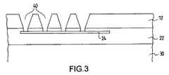
このため、接続端子に電気的に連結するための導電ランド24の各々の上方に分布した一連の開口40が、エピタキシャル層12の厚さ全体を貫通して開口される。場合によっては、単一の開口40で十分であり得るが、すべての場合において開口はランド24の導電部の上方に位置する。図3はランド24とこのランドの上方に形成された開口40とを備える集積回路の一部の図を表わす。少数の局所的開口のみを示して図を簡略化している。層12のシリコンの厚さ全体を貫通してこれらの開口をエッチングした後、開口の底部に位置する絶縁層22の一部を除去して開口を完成させることにより導電ランド24を露出させる。 For this reason, a series of openings 40 distributed above each of the
導電層42、例えばアルミニウムをその後堆積する。以後、層16(導電ランド24を含むもの)を第1の導電層と称し、層42を第2の導電層と称するが、2つの導電層は、集積回路に対する外部接続端子を形成する役目を果たす。第2の導電層42の堆積の前に、シリコンを表面ドーピングするステップを行ってもよい。 A
第2の導電層42は開口を充填し、これらの開口の各々を介して、ランド24を形成する第1の導電層と接する(図4)。 The second
この堆積後、第2の導電層42をエッチングして外部接続端子を画定する。図5は接続端子の全体図を表わし、好ましくは、部分44(図の左側)にランド24の上方に分布した開口が穿孔され、他の部分46には接続ワイヤをはんだ付けするために確保される開口(図の右側)が穿孔されていない。なお個々の開口が十分に小さい場合には、表面領域全体が開口の規則的分布を備える接続端子を有し、その後ワイヤが開口40により作製されるリリーフを含む金属表面領域にはんだ付けされるように考えることも可能であり、その際ランド24は接続端子の下に位置する表面領域の大部分またはすべてを占有することになる。 After this deposition, the second
図6は以下のステップを表わす。周囲トレンチ48をエッチングして、エピタキシャル層の厚さ全体を貫通して絶縁層22まで接続端子を完全に取り囲む。このトレンチは絶縁層22で停止し、金属層の一部まで下がらないため、トレンチの底部は全体に絶縁表面によって形成される。 FIG. 6 represents the following steps. The
以下のステップ、図7は必須ではないが好ましい。ステップは絶縁保護層50の堆積と、導電端子の中心の上方のこの層の開口とを含む(そのため開口で穿孔されずワイヤのはんだ付け用に確保される一部が設けられている場合には、基本的には端子の部分46内)。絶縁層50は周囲トレンチ48を充填する。 The following steps, FIG. 7, are preferred but not essential. The steps include the deposition of the insulating
色フィルタの堆積および光エッチング用の従来のステップは表わされていない。 Conventional steps for color filter deposition and photoetching are not represented.
最後にウェハを個々のチップに切断した後、最終的作製ステップは、露出されている部分における接続端子の金属42への接続ワイヤ60のはんだ付けを含む(図8)。 Finally, after the wafer is cut into individual chips, the final fabrication step involves soldering the
下層24を有するその多数のコンタクトホールを有し、且つホールのない部分を有する接続端子の全体的外観が図9の平面図に示されている。小さい寸法(数マイクロメートルの直径または辺寸法)の数十のホールを設けることが好ましいが、前述したように場合によっては単一のホールで十分であり得る。 The overall appearance of the connection terminal with its many contact holes with the
接続端子はこのように、接続金属42を堆積する前に開口40の側面に絶縁層を堆積せずに作製されている。金属42はシリコンと接しているが、シリコンはトレンチによって、アクティブ回路を含むエピタキシャル層の残りの部分から絶縁されているため、集積回路の外部または内部のいずれかから端子に印加される電位は、回路の他の部分または他の端子に影響を及ぼさない。 Thus, the connection terminal is produced without depositing an insulating layer on the side surface of the opening 40 before depositing the
最後の保護層50があるか否かにかかわらず、樹脂またはフィルタリング層の拡散は接続端子の存在によって阻害されない。層50がある場合これらは中空であるが、端子の表面と層50の表面との段差は小さい。層50がない場合には、金属によりさらに部分的に充填される開口40は小さい寸法(数マイクロメートルの辺または直径寸法)のものであり、拡散を阻害しない。さらにまた、接続端子の表面と周囲表面との間に凹部がないことにより、端子の寸法を約50〜60マイクロメートルの辺寸法、集積回路チップの上面に対して深すぎる金属表面では考えられない限界に制限することができる。 Regardless of whether the last
開口40はシリコンへの化学的腐食によって好ましくは形成され、その際開口は傾斜側部を有し、その角度はシリコンの自然劈開面に相当(55°)する。トレンチ48は垂直異方性腐食(プラズマエッチング)によって好ましくはエッチングされ、その側面は垂直である。その幅は数マイクロメートル(例えば1〜3マイクロメートル)であり得る。トレンチ48は開口40と同時には作製されないため(これは理論的には可能であるが)、層42が堆積されるときにアルミニウムで充填されないが、それは接続端子を画定するためにエッチングする際にトレンチの底部からアルミニウムを排除することが困難だからである。 The opening 40 is preferably formed by chemical erosion to silicon, in which case the opening has inclined sides, the angle of which corresponds to the natural cleavage plane of silicon (55 °). The
Claims (7)
Translated fromJapanese前記シリコン基板の前面から実施する、光電素子と少なくとも1つの絶縁層(22)および第1の導電層(24)を形成し、該形成後のシリコン基板の前面を転写基板に転写し、該転写後のシリコン基板を薄膜化する作製工程と、該薄膜化したシリコン基板の背面から実施する作製工程とを含み、
前記背面から実施する作製工程は、
前記薄膜化したシリコン基板(12)を貫通する、前記センサー用の外部接続端子を作製するために確保されたパッド領域(44、46)の第1の部分(44)上にある少なくとも1つの局所的な開口(40)をエッチングし、該開口(40)内の前記第1の導電層を露出させる工程と、
前記開口(40)内および開口(40)外の前記シリコン基板(12)のシリコンと接し、前記開口内の露出した前記第1の導電層に接する第2の導電層(42)を堆積する工程と、
前記パッド領域内に構成され、前記開口(40)内および開口(40)外の前記シリコンと接し前記開口(40)内の前記第1の導電層に接する接続端子を画定するように前記第2の導電層をエッチングする工程と、
前記シリコン基板(12)の厚み全体を貫通して前記絶縁層まで達する深さの周囲トレンチ(48)をエッチングする工程であって、前記周囲トレンチが前記パッド領域全体を取り囲み、前記周囲トレンチの底部が前記絶縁層で形成されて、前記接続端子によって覆われた薄膜シリコンの島を形成するとともに、前記シリコン基板(12)の前記島と該島の外の残りの部分とを絶縁し、前記残りの部分に前記光電素子が配置されるように前記周囲トレンチをエッチングする工程を含むことを特徴とするシリコン基板上の画像センサの作製方法。A method for producing an image sensor on a silicon substrate, comprising:
The photoelectric element and at least one insulating layer (22) and the first conductive layer (24) are formed from the front surface of the silicon substrate, the front surface of the silicon substrate after the formation is transferred to the transfer substrate, and the transfer Including a manufacturing step of thinning the subsequent silicon substrate, and a manufacturing step performed from the back side of the thinned silicon substrate,
The manufacturing process carried out from the back side
At least one local area on the first portion (44 ) of the pad region (44, 46) reserved for producing the external connection terminal for the sensor, which penetrates the thinned silicon substrate (12). Etching a typical opening (40) to expose the first conductive layer in the opening (40);
Depositing a second conductive layer (42) in contact with the silicon of the silicon substrate (12) in the opening (40) and outside the opening (40) and in contact with the exposed first conductive layer in the opening; When,
The second region is formed in the pad region and defines a connection terminal in contact with the silicon in the opening (40) and outside the opening (40) and in contact with the first conductive layer in the opening (40). Etching the conductive layer of
Etching a peripheral trench (48) having a depth that penetrates the entire thickness of the silicon substrate (12) to reach the insulating layer, the peripheral trench surrounding the entire pad region, and the bottom of the peripheral trench Is formed of the insulating layer to form an island of thin film silicon covered by the connection terminal, and insulates the island of the silicon substrate (12) from the remaining portion outside the island, And a step of etching the surrounding trench so that the photoelectric element is disposed at a portion of the image sensor.
前記開口(40)から隔絶した第2の部分(46)を有し、
前記ワイヤは、
前記パッド領域の前記第2の部分の前記第2の導電層にはんだ付けされることを特徴とする請求項2記載のシリコン基板上の画像センサの作製方法。The pad area is
A second portion (46) isolated from the opening (40);
The wire is
3. The method for manufacturing an image sensor on a silicon substrate according to claim 2, wherein the image sensor is soldered to the second conductive layer of the second portion of the pad region.
化学的腐食によるエッチングによって前記シリコン基板(12)の背面側から前記シリコンの自然劈開面に相当する角度で傾斜する傾斜側部を形成して作製され、
前記周囲トレンチは、
前記第2の導電層のエッチング後に作製されることを特徴とする請求項1乃至4のいずれかに記載のシリコン基板上の画像センサの作製方法。The opening (40)
It is produced by forming an inclined side portion inclined at an angle corresponding to the natural cleavage plane of the silicon from the back side of the silicon substrate (12) by etching by chemical corrosion,
The surrounding trench is
The method for manufacturing an image sensor on a silicon substrate according toclaim 1, wherein the image sensor is manufactured after etching the second conductive layer.
垂直異方性腐食によるエッチングによって作製されることを特徴とする請求項1乃至5のいずれかに記載のシリコン基板上の画像センサの作製方法。The surrounding trench is
6. The method for producing an image sensor on a silicon substrate according to claim 1, wherein the image sensor is produced by etching by vertical anisotropic corrosion.
前記パッド領域の前記第1の部分内に割り当てられる一連の開口であることを特徴とする請求項1乃至6のいずれかに記載のシリコン基板上の画像センサの作製方法。The opening (40)
7. The method of manufacturing an image sensor on a silicon substrate according to claim 1, wherein theopening is a series of openings allocated in the first portion of the pad region.
Applications Claiming Priority (3)
| Application Number | Priority Date | Filing Date | Title |
|---|---|---|---|
| FR0513221AFR2895566B1 (en) | 2005-12-23 | 2005-12-23 | AMINOUS IMAGE SENSOR WITH INSULATED CONTACT PLOTS BY TRANCHEE |
| FR05/13221 | 2005-12-23 | ||
| PCT/EP2006/068107WO2007071491A1 (en) | 2005-12-23 | 2006-11-06 | Thinned image sensor having trench-isolated contact pads |
Publications (2)
| Publication Number | Publication Date |
|---|---|
| JP2009521111A JP2009521111A (en) | 2009-05-28 |
| JP5272176B2true JP5272176B2 (en) | 2013-08-28 |
Family
ID=36933513
Family Applications (1)
| Application Number | Title | Priority Date | Filing Date |
|---|---|---|---|
| JP2008546311AExpired - Fee RelatedJP5272176B2 (en) | 2005-12-23 | 2006-11-06 | Manufacturing method of image sensor having trench insulating contact terminal |
Country Status (8)
| Country | Link |
|---|---|
| US (1) | US7998780B2 (en) |
| EP (1) | EP1964176B8 (en) |
| JP (1) | JP5272176B2 (en) |
| KR (1) | KR101287308B1 (en) |
| CN (1) | CN101366119A (en) |
| CA (1) | CA2634599C (en) |
| FR (1) | FR2895566B1 (en) |
| WO (1) | WO2007071491A1 (en) |
Families Citing this family (3)
| Publication number | Priority date | Publication date | Assignee | Title |
|---|---|---|---|---|
| FR2910707B1 (en)* | 2006-12-20 | 2009-06-12 | E2V Semiconductors Soc Par Act | IMAGE SENSOR WITH HIGH DENSITY INTEGRATION |
| TWI388038B (en)* | 2009-07-23 | 2013-03-01 | Ind Tech Res Inst | Structure and fabrication method of a sensing device |
| EP3376531B1 (en) | 2014-02-28 | 2023-04-05 | LFoundry S.r.l. | Semiconductor device comprising a laterally diffused transistor |
Family Cites Families (5)
| Publication number | Priority date | Publication date | Assignee | Title |
|---|---|---|---|---|
| FR2829291B1 (en)* | 2001-08-31 | 2005-02-04 | Atmel Grenoble Sa | METHOD FOR MANUFACTURING COLOR IMAGE SENSOR WITH HOLLOW CONTACT OPENINGS BEFORE SLOWDOWN |
| FR2829875B1 (en) | 2001-09-14 | 2004-01-02 | Atmel Grenoble Sa | IMAGE SENSOR WITH PLANARIZING LAYERS AND MANUFACTURING PROCESS |
| JP4046069B2 (en)* | 2003-11-17 | 2008-02-13 | ソニー株式会社 | Solid-state imaging device and manufacturing method of solid-state imaging device |
| JP2005167090A (en)* | 2003-12-04 | 2005-06-23 | Hamamatsu Photonics Kk | Semiconductor light receiving element and manufacturing method therefor |
| JP4525129B2 (en)* | 2004-03-26 | 2010-08-18 | ソニー株式会社 | Solid-state imaging device and manufacturing method thereof, and semiconductor integrated circuit device and manufacturing method thereof |
- 2005
- 2005-12-23FRFR0513221Apatent/FR2895566B1/ennot_activeExpired - Fee Related
- 2006
- 2006-11-06KRKR1020087015293Apatent/KR101287308B1/ennot_activeExpired - Fee Related
- 2006-11-06CNCNA2006800515887Apatent/CN101366119A/enactivePending
- 2006-11-06JPJP2008546311Apatent/JP5272176B2/ennot_activeExpired - Fee Related
- 2006-11-06USUS12/158,947patent/US7998780B2/ennot_activeExpired - Fee Related
- 2006-11-06CACA2634599Apatent/CA2634599C/ennot_activeExpired - Fee Related
- 2006-11-06WOPCT/EP2006/068107patent/WO2007071491A1/enactiveApplication Filing
- 2006-11-06EPEP06807744.5Apatent/EP1964176B8/ennot_activeNot-in-force
Also Published As
| Publication number | Publication date |
|---|---|
| KR101287308B1 (en) | 2013-07-17 |
| CA2634599C (en) | 2015-06-09 |
| FR2895566B1 (en) | 2008-04-18 |
| KR20080080997A (en) | 2008-09-05 |
| JP2009521111A (en) | 2009-05-28 |
| EP1964176A1 (en) | 2008-09-03 |
| FR2895566A1 (en) | 2007-06-29 |
| CN101366119A (en) | 2009-02-11 |
| WO2007071491A1 (en) | 2007-06-28 |
| EP1964176B8 (en) | 2018-04-04 |
| US7998780B2 (en) | 2011-08-16 |
| EP1964176B1 (en) | 2018-01-03 |
| US20090263931A1 (en) | 2009-10-22 |
| CA2634599A1 (en) | 2007-06-28 |
Similar Documents
| Publication | Publication Date | Title |
|---|---|---|
| JP4966487B2 (en) | Semiconductor device and manufacturing method thereof | |
| CN101937894B (en) | Semiconductor device including through-electrode and method of manufacturing the same | |
| KR100679573B1 (en) | Manufacturing Method of Semiconductor Device | |
| CN100382247C (en) | Manufacturing method of semiconductor device | |
| US8487422B2 (en) | Chip stack with conductive column through electrically insulated semiconductor region | |
| KR101264926B1 (en) | Method of manufacturing semiconductor device and semiconductor device | |
| US20090039471A1 (en) | Semiconductor device | |
| EP0583877B1 (en) | Bond pad structure of an integrated circuit and manufacturing method thereof | |
| JP2006100435A (en) | Semiconductor device and manufacturing method thereof | |
| JP2006310726A (en) | Semiconductor device and manufacturing method thereof | |
| EP2002477B1 (en) | A fabrication method for a low ohmic through substrate connection for semiconductor carriers | |
| US5474651A (en) | Method for filling via holes in a semiconductor layer structure | |
| JP2006269860A (en) | Through-conductor and its manufacturing method | |
| JP4863214B2 (en) | Manufacturing method of electronic chip made of thinned silicon | |
| JP5272176B2 (en) | Manufacturing method of image sensor having trench insulating contact terminal | |
| US7898052B2 (en) | Component with a semiconductor junction and method for the production thereof | |
| JP2007095950A (en) | Semiconductor device and manufacturing method thereof | |
| US7485926B2 (en) | SOI contact structures | |
| US9847365B2 (en) | Electronic component and method of manufacturing the same | |
| JPH0438875A (en) | Semiconductor device and manufacture method thereof | |
| JP4284748B2 (en) | Semiconductor device and manufacturing method thereof | |
| KR100943485B1 (en) | Manufacturing method of semiconductor device | |
| KR20010046388A (en) | Forming method of pad | |
| JP2008124271A (en) | Semiconductor device | |
| KR20010019715A (en) | Structure for pad in semiconductor device and manufacturing method thereof |
Legal Events
| Date | Code | Title | Description |
|---|---|---|---|
| A621 | Written request for application examination | Free format text:JAPANESE INTERMEDIATE CODE: A621 Effective date:20091005 | |
| A521 | Request for written amendment filed | Free format text:JAPANESE INTERMEDIATE CODE: A523 Effective date:20101215 | |
| A977 | Report on retrieval | Free format text:JAPANESE INTERMEDIATE CODE: A971007 Effective date:20111125 | |
| A131 | Notification of reasons for refusal | Free format text:JAPANESE INTERMEDIATE CODE: A131 Effective date:20111129 | |
| A601 | Written request for extension of time | Free format text:JAPANESE INTERMEDIATE CODE: A601 Effective date:20120227 | |
| A521 | Request for written amendment filed | Free format text:JAPANESE INTERMEDIATE CODE: A523 Effective date:20120323 | |
| A521 | Request for written amendment filed | Free format text:JAPANESE INTERMEDIATE CODE: A523 Effective date:20120425 | |
| A602 | Written permission of extension of time | Free format text:JAPANESE INTERMEDIATE CODE: A602 Effective date:20120319 | |
| A131 | Notification of reasons for refusal | Free format text:JAPANESE INTERMEDIATE CODE: A131 Effective date:20121002 | |
| A521 | Request for written amendment filed | Free format text:JAPANESE INTERMEDIATE CODE: A523 Effective date:20121221 | |
| A01 | Written decision to grant a patent or to grant a registration (utility model) | Free format text:JAPANESE INTERMEDIATE CODE: A01 Effective date:20130122 | |
| A61 | First payment of annual fees (during grant procedure) | Free format text:JAPANESE INTERMEDIATE CODE: A61 Effective date:20130213 | |
| A61 | First payment of annual fees (during grant procedure) | Free format text:JAPANESE INTERMEDIATE CODE: A61 Effective date:20130418 | |
| R150 | Certificate of patent or registration of utility model | Free format text:JAPANESE INTERMEDIATE CODE: R150 | |
| R250 | Receipt of annual fees | Free format text:JAPANESE INTERMEDIATE CODE: R250 | |
| LAPS | Cancellation because of no payment of annual fees |