JP5271170B2 - Image display element and manufacturing method thereof - Google Patents
Image display element and manufacturing method thereofDownload PDFInfo
- Publication number
- JP5271170B2 JP5271170B2JP2009152432AJP2009152432AJP5271170B2JP 5271170 B2JP5271170 B2JP 5271170B2JP 2009152432 AJP2009152432 AJP 2009152432AJP 2009152432 AJP2009152432 AJP 2009152432AJP 5271170 B2JP5271170 B2JP 5271170B2
- Authority
- JP
- Japan
- Prior art keywords
- image display
- display element
- metal film
- front panel
- electrode
- Prior art date
- Legal status (The legal status is an assumption and is not a legal conclusion. Google has not performed a legal analysis and makes no representation as to the accuracy of the status listed.)
- Expired - Fee Related
Links
Images


Classifications
- G—PHYSICS
- G02—OPTICS
- G02F—OPTICAL DEVICES OR ARRANGEMENTS FOR THE CONTROL OF LIGHT BY MODIFICATION OF THE OPTICAL PROPERTIES OF THE MEDIA OF THE ELEMENTS INVOLVED THEREIN; NON-LINEAR OPTICS; FREQUENCY-CHANGING OF LIGHT; OPTICAL LOGIC ELEMENTS; OPTICAL ANALOGUE/DIGITAL CONVERTERS
- G02F1/00—Devices or arrangements for the control of the intensity, colour, phase, polarisation or direction of light arriving from an independent light source, e.g. switching, gating or modulating; Non-linear optics
- G02F1/01—Devices or arrangements for the control of the intensity, colour, phase, polarisation or direction of light arriving from an independent light source, e.g. switching, gating or modulating; Non-linear optics for the control of the intensity, phase, polarisation or colour
- G02F1/13—Devices or arrangements for the control of the intensity, colour, phase, polarisation or direction of light arriving from an independent light source, e.g. switching, gating or modulating; Non-linear optics for the control of the intensity, phase, polarisation or colour based on liquid crystals, e.g. single liquid crystal display cells
- G02F1/133—Constructional arrangements; Operation of liquid crystal cells; Circuit arrangements
- G02F1/1333—Constructional arrangements; Manufacturing methods
- G02F1/13336—Combining plural substrates to produce large-area displays, e.g. tiled displays
- G—PHYSICS
- G02—OPTICS
- G02F—OPTICAL DEVICES OR ARRANGEMENTS FOR THE CONTROL OF LIGHT BY MODIFICATION OF THE OPTICAL PROPERTIES OF THE MEDIA OF THE ELEMENTS INVOLVED THEREIN; NON-LINEAR OPTICS; FREQUENCY-CHANGING OF LIGHT; OPTICAL LOGIC ELEMENTS; OPTICAL ANALOGUE/DIGITAL CONVERTERS
- G02F1/00—Devices or arrangements for the control of the intensity, colour, phase, polarisation or direction of light arriving from an independent light source, e.g. switching, gating or modulating; Non-linear optics
- G02F1/01—Devices or arrangements for the control of the intensity, colour, phase, polarisation or direction of light arriving from an independent light source, e.g. switching, gating or modulating; Non-linear optics for the control of the intensity, phase, polarisation or colour
- G02F1/13—Devices or arrangements for the control of the intensity, colour, phase, polarisation or direction of light arriving from an independent light source, e.g. switching, gating or modulating; Non-linear optics for the control of the intensity, phase, polarisation or colour based on liquid crystals, e.g. single liquid crystal display cells
- G02F1/133—Constructional arrangements; Operation of liquid crystal cells; Circuit arrangements
- G02F1/1333—Constructional arrangements; Manufacturing methods
- G02F1/1345—Conductors connecting electrodes to cell terminals
- H—ELECTRICITY
- H10—SEMICONDUCTOR DEVICES; ELECTRIC SOLID-STATE DEVICES NOT OTHERWISE PROVIDED FOR
- H10K—ORGANIC ELECTRIC SOLID-STATE DEVICES
- H10K59/00—Integrated devices, or assemblies of multiple devices, comprising at least one organic light-emitting element covered by group H10K50/00
- H10K59/10—OLED displays
- H10K59/12—Active-matrix OLED [AMOLED] displays
- H10K59/131—Interconnections, e.g. wiring lines or terminals
- H—ELECTRICITY
- H10—SEMICONDUCTOR DEVICES; ELECTRIC SOLID-STATE DEVICES NOT OTHERWISE PROVIDED FOR
- H10K—ORGANIC ELECTRIC SOLID-STATE DEVICES
- H10K59/00—Integrated devices, or assemblies of multiple devices, comprising at least one organic light-emitting element covered by group H10K50/00
- H10K59/10—OLED displays
- H10K59/17—Passive-matrix OLED displays
- H10K59/179—Interconnections, e.g. wiring lines or terminals
- H10K59/1795—Interconnections, e.g. wiring lines or terminals comprising structures specially adapted for lowering the resistance
Landscapes
- Physics & Mathematics (AREA)
- Nonlinear Science (AREA)
- Optics & Photonics (AREA)
- Crystallography & Structural Chemistry (AREA)
- Chemical & Material Sciences (AREA)
- General Physics & Mathematics (AREA)
- Mathematical Physics (AREA)
- Engineering & Computer Science (AREA)
- Microelectronics & Electronic Packaging (AREA)
- Devices For Indicating Variable Information By Combining Individual Elements (AREA)
- Electroluminescent Light Sources (AREA)
- Liquid Crystal (AREA)
- Gas-Filled Discharge Tubes (AREA)
Abstract
Description
Translated fromJapanese本発明は、例えば、液晶ディスプレイ(LCD)パネル、プラズマディスプレイパネル(PDP)、エレクトロルミネッセント(EL)ディスプレイパネル等を多数配列して構成される大型画像表示装置に関し、特に、この装置を構成する画像表示素子とその製造方法に関するものである。 The present invention relates to a large-sized image display device configured by arranging a large number of liquid crystal display (LCD) panels, plasma display panels (PDP), electroluminescent (EL) display panels, and the like, for example. The present invention relates to an image display element to be manufactured and a manufacturing method thereof.
大型画像表示装置(大型ディスプレイとも称す)は、低価格で高性能を実現するために、画像表示素子(又は、表示ユニット)としての平面ディスプレイ(例えば、LCDパネル、PDP、ELディスプレイパネル等)をマトリクス状に複数枚配列する方式が採用されている。
このような大型ディスプレイを構成する従来の画像表示素子の一例を図13に示す。
図13は、画像表示素子の配列の一部(2枚配列)を示す図で、図13(a)は正面図、図13(b)は側面図である。
画像表示素子30は、ガラス板などからなる前面パネル31と裏面パネル32とを有する。前面パネル31と裏面パネル32は、所定の間隔をあけて対向させ、その間に、複数の画素33と、それらを制御するための複数の電極(図示なし)とを配置して発光層(又は液晶層)を形成し、周囲を封止幅g1の封止部34で封止している。A large image display device (also referred to as a large display) is a flat display (for example, LCD panel, PDP, EL display panel, etc.) as an image display element (or display unit) in order to achieve high performance at a low price. A method of arranging a plurality of sheets in a matrix is employed.
An example of a conventional image display element constituting such a large display is shown in FIG.
13A and 13B are diagrams showing a part of the arrangement of the image display elements (two-sheet arrangement). FIG. 13A is a front view and FIG. 13B is a side view.
The
電極に電圧を印加するための引出線を、画像表示素子30の周囲、即ち隣接する画像表示素子30の継ぎ目部35から引き出す場合は、引出し代が必要である。継ぎ目部35における隣接する画像表示素子30の画素33の間隔Gaが、同一の画像表示素子内における画素の間隔Gbより大きくなると、継ぎ目部35が目立ってしまう。
そこで、図13(b)の拡大図に示すように、裏面パネル32を2分割して中央部にギャップ部36を設け、そのギャップ部(単に、ギャップとも称す)36に電極に対応させた端子37を備え、この端子37に電極ピンあるいは図のような引出線38を接続して裏面パネルの外側に引き出すようにしている(例えば、特許文献1参照)。In the case where a lead line for applying a voltage to the electrode is drawn out from the periphery of the
Therefore, as shown in the enlarged view of FIG. 13B, the
特許文献1に示された従来の画像表示素子では、裏面パネル32に形成したギャップ部36から電極の引出線38を引き出すようにしたので、画像表示素子30の継ぎ目部35を目立ち難くする構造としては有効であるが、狭いギャップ部36の間に存在する多数の端子37に引出線38を接続して配線層と接続するようになっているため、端子37との接続が煩雑となり、また、引出し方法が複雑で作業性が悪いという問題があった。 In the conventional image display element disclosed in
特許文献2に示された従来の画像表示素子は、このような問題点を解消するために提供されたものである。
図14は、特許文献2に示された画像表示素子の構成を示す斜視図であり、図15は図14の要部拡大図である。
以下、特許文献2に示される従来の画像表示素子について説明する。
この画像表示素子がマトリクス状に多数配列されて、大画面の平面ディスプレイが構成される。
画像表示素子の表示デバイスとしては、例えば、LCDパネル、PDP、ELディスプレイパネル等である。なお、図は画像表示素子を背面から見たところを示している。The conventional image display element disclosed in
FIG. 14 is a perspective view showing the configuration of the image display element disclosed in
Hereinafter, a conventional image display element disclosed in
A large number of image display elements are arranged in a matrix to form a large screen flat display.
Examples of the display device of the image display element include an LCD panel, a PDP, and an EL display panel. The figure shows the image display element as viewed from the back.
図14に示すように、画像表示素子は、ガラス板等からなる前面パネル21と、同じくガラス板等からなり前面パネル21に対向する裏面パネル22と、両パネル間にマトリクス状に配置されて表示又は非表示の状態が選択される複数の画素(図示なし)と、この画素を制御する複数の電極(図示なし)とを有し、両パネル21、22が画素及び電極を挟んで貼り合わされて構成されている。
裏面パネル22は、隣り合う2つの画素列の間で分割されてその分割部に隙間(ギャップ)23が形成されている。図では、分かりやすいように隙間23を拡大して表示しているが、実際の隙間23は、例えば、幅0.30mm程度の微小隙間である。
また、画素はマトリクス状に配置されているので、画素間をいうとき、横方向の画素行間と縦方向の画素列間が存在するが、両方を含めて「隣り合う2つの画素列」とする。As shown in FIG. 14, the image display element is displayed by being arranged in a matrix between a
The
In addition, since the pixels are arranged in a matrix, when referring to between the pixels, there are horizontal pixel rows and vertical pixel columns, but both include “two adjacent pixel columns”. .
なお、裏面パネル2は中央部で2分割したものを示しているが、分割数と分割位置はこれに限定するものではない。裏面パネル22を3分割以上にしてもよく、分割する位置も、隣接する画素の間であれば他の位置であってもよい。
隙間23に位置する前面パネル21側には、電極に繋がる複数の電極端子24が配置されている。電極端子24は、例えば、電極と同じ材料で同時に形成されたものであり、隙間から露出させている。
一方、裏面パネル22の裏面22a(前面パネルとの対向面の裏側を裏面と称す)と隙間(ギャップ)23の端部である端面22bには、金属膜配線25が形成されている。
金属膜配線25は、例えば、厚膜印刷等によって形成されるものである。裏面22a側の金属膜配線25の端部にコネクタ26を接続している。このコネクタ26を介して外部の駆動回路に接続される。In addition, although the
A plurality of
On the other hand, on the
The
配線部の詳細を図15に示す。図のように、裏面パネル22を前面パネル21に貼り合わせた状態で、裏面パネル22の端部22bの金属膜配線25が前面パネル21側の電極端子24に垂直に当接するように、電極端子24と金属膜配線25の位置を合わせて形成されている。そして、両パネル21、22を貼り合わせた状態で当接部分に半田27を塗布し、局部的に加熱して半田27を溶かして接合する。
また、図16は、前面パネル21の外周端部から電極端子24を引き出した場合の電極接続部を示す斜視図である。
裏面パネル22を前面パネル21よりわずかに小さくし、両パネルを重ねたときに端部に段差部21aを形成するようにし、この段差部21aに電極端子24を露出させ、電極端子24と裏面パネル22の端部22bに形成した金属膜配線25を当接させ、半田付けによって接合する場合の構成を示している。Details of the wiring section are shown in FIG. As shown in the figure, in a state where the
FIG. 16 is a perspective view showing an electrode connecting portion when the
The
以上のように、特許文献2に示される画像表示素子は、前面パネル21と、前面パネル21に対向する裏面パネル22と、両パネル間にマトリクス状に配置されて表示または非表示の状態が選択される複数の画素(図示なし)と、この画素を制御する複数の電極とを有し、両パネルが画素及び電極を挟んで貼り合わされて構成される画像表示素子において、裏面パネル22の裏面と端面(端部22bの面)とに金属膜配線25が形成され、裏面パネル22の端面に形成された金属膜配線25に対応し、電極に繋がる電極端子24が前面パネル21側に配置され、端面22bに形成された金属膜配線25と電極端子24とが半田付けにより接合されている。
従って、特許文献1に示された画像表示素子に比べて、電極の引出線を用いることなく、狭いスペースから簡単な方法で電極の引出しが可能となり、画像表示素子間の目地幅が広がるのが解消されて、画像表示素子を配列して大画面を構成する場合、目地縮小により画質が改善される。また、電極配線の引出しが簡素化され、コストが削減される。As described above, the image display element disclosed in
Therefore, compared with the image display element shown in
特許文献2に示す従来の画像表示素子は、図14に示したように、電極端子24と金属膜配線25を直接半田付けして接続するので、裏面パネル22に形成したギャップ(隙間/溝部)23から電極の引出しが可能である。
しかしながら、画像表示素子の継ぎ目部を目立ち難くする構造としては有効であるが、やはり裏面パネル22の厚みに対応して生じる端子部付近の溝部(ギャップ部)では、加工用の工具(半田付けのための工具のヘッドやニードルなど)がギャップ(溝部/隙間)23の奥にある半田付け部(即ち、電極端子24と金属膜配線25の当接部)に届き難くなる。
特に、表示装置が高解像度化するにつれて、画素ピッチが短縮され、画素ピッチの短縮に対応して電極の引出しを行うギャップ部の幅も狭くする必要があり、電極の引出し加工が更に困難になる。
従って、半田付けによる電極端子24と金属膜配線25の接続信頼性が問題になる。
また、電極端子24と金属膜配線25を接続する半田27が微小の間隔を有して配置されるので、隣接する電極端子間、金属膜配線間あるいは半田間においてマイグレーションが発生しやすく、電極引出部の絶縁性が問題となる。As shown in FIG. 14, in the conventional image display element shown in
However, although it is effective as a structure that makes the joint portion of the image display element inconspicuous, a processing tool (soldering) is also used in the groove portion (gap portion) near the terminal portion that also corresponds to the thickness of the
In particular, as the display device becomes higher in resolution, the pixel pitch is shortened, and it is necessary to reduce the width of the gap part for drawing out the electrode corresponding to the shortening of the pixel pitch, which makes the drawing of the electrode more difficult. .
Therefore, the connection reliability between the
In addition, since the
また、図16に示した従来の画像表示素子では、パネルの外周端部から容易に電極を引き出すことはできるが、電極の引出し線を設ける端子部付近のパネル形状に課題があり、電極の引出し加工が難しくなる。
加工方法は、例えば、半田付け、ワイヤボンディング、導電ペーストなどによる接続などがあるが、裏面パネル22の厚みに対応して生じる端子部付近の段差部では、加工用の工具(ヘッドなど)などが段差部の奥にある接続部に届き難い。In the conventional image display element shown in FIG. 16, the electrode can be easily pulled out from the outer peripheral edge of the panel. However, there is a problem in the panel shape near the terminal portion where the lead wire for the electrode is provided. Processing becomes difficult.
The processing method includes, for example, connection by soldering, wire bonding, conductive paste, and the like. However, a processing tool (such as a head) is used at a step portion near the terminal portion corresponding to the thickness of the
また、従来の画像表示素子では、裏面パネル22は、ギャップ部23で分割されているので、この部分にストレスが集中すると強度が弱くなるという問題もあった。 Further, in the conventional image display element, since the
この発明は、上記のような問題点を解決するためになされたものであり、画像表示素子の端子部付近のパネル形状を電極の引出し電極の引出し加工に必要な工具(即ち、半田コテのヘッドや導電ペースト注入用のニードルなど)の使用に適した構造にすることにより電極の引出し加工を容易に行えると共に、更に、電極引出部(電極端子と金属膜配線の接続部)におけるマイグレーションの発生を抑制できる画像表示装置及び画像表示装置の製造方法を提供することを目的とする。 The present invention has been made in order to solve the above-mentioned problems. A panel shape in the vicinity of a terminal portion of an image display element is a tool necessary for drawing out an electrode lead electrode (that is, a soldering iron head). In addition, the electrode can be easily pulled out by adopting a structure suitable for the use of the needle for injecting the conductive paste, etc., and further, the occurrence of migration in the electrode lead-out portion (connecting portion between the electrode terminal and the metal film wiring) can be prevented. An object of the present invention is to provide an image display device that can be suppressed and a method for manufacturing the image display device.
この発明に係わる画像表示素子は、前面パネルと、この前面パネルに対向する裏面パネルと、前記前面パネル及び裏面パネル間にマトリクス状に配置されて表示又は非表示の状態が選択される複数の画素と、この画素を制御する複数の電極とを有し、前記前面パネルと前記裏面パネルが画素及び電極を挟んで貼り合わされて構成され、金属膜配線を介して前記電極を駆動回路に接続する画像表示素子において、
前記裏面パネルは、隣り合う複数の画素列の間で前記電極に繋がる電極端子が露出するように分割されると共に、この分割部分に前記前面パネルとの対向面の裏側にある上部が底部より幅広の形状を有する溝部が形成されており、前記金属膜配線は、前記裏面パネルの前記前面パネルとの対向面の裏側の面に形成されており、前記電極端子と前記金属膜配線は、前記溝部を構成する傾斜面に沿って塗布された導電ペーストにより接続されているものである。An image display element according to the present invention includes a front panel, a back panel facing the front panel, and a plurality of pixels arranged in a matrix between the front panel and the back panel to select a display or non-display state. And a plurality of electrodes for controlling the pixel, and the front panel and the back panel are bonded to each other with the pixel and the electrode interposed therebetween, and the electrode is connected to the drive circuit through the metal film wiring. In the display element,
The back panel, together with the electrode terminals connected to the electrodes between a plurality of adjacent pixel lines are divided so as to expose the upper on the back of the facing surfaces of thefront panel in the divided portion from the bottom portion groove having a shape wider and is formed, the metal film wires, the said being formed on the back surface of the facing surfaces of thefront panel of the back panel, the metal film wiring and the electrode terminal, They are connected by a conductive paste applied along an inclined surface constituting the groove.
また、この発明に係わる画像表示素子の製造方法は、前面パネルと、この前面パネルに対向する裏面パネルと、前記前面パネル及び裏面パネル間にマトリクス状に配置されて表示又は非表示の状態が選択される複数の画素と、この画素を制御する複数の電極とを有し、前記前面パネルと前記裏面パネルが画素及び電極を挟んで貼り合わされて構成され、金属膜配線を介して前記電極を駆動回路に接続する画像表示素子の製造方法において、
前記裏面パネルを、隣り合う複数の画素列の間で前記電極に繋がる電極端子が露出するように分割すると共に、この分割部分に前記前面パネルとの対向面の裏側にある上部が底部より幅広の形状を有する溝部を形成する第1の工程と、前記金属膜配線を、前記裏面パネルの前記前面パネルとの対向面の裏側の面に形成する第2の工程と、前記電極端子と前記金属膜配線を、前記溝部を構成する傾斜面に沿って塗布された導電ペーストにより接続する第3の工程を有するものである。The image display element manufacturing method according to the present invention includes a front panel, a back panel opposite to the front panel, and a display or non-display state arranged in a matrix between the front panel and the back panel. A plurality of pixels to be controlled and a plurality of electrodes for controlling the pixels, and the front panel and the back panel are bonded to each other with the pixels and the electrodes interposed therebetween, and the electrodes are driven through a metal film wiring. In a method for manufacturing an image display element connected to a circuit,
Said back panel, a plurality of electrode terminals connected to the electrodes between the adjacent pixel lines are divided so as to expose, wider than the upper bottom on the back of the facing surfaces of thefront panel to the divided portion wherein a first step of forming a groove having a shape, the metal film wires, and a second step of forming on the back surface of the facing surfaces of thefront panel of the back panel, and the electrode terminal The method includes a third step of connecting the metal film wiring with a conductive paste applied along the inclined surface constituting the groove.
この発明によれば、電極の引出し加工を容易に行えると共に、電極引出部(電極端子と金属膜配線の接続部)におけるマイグレーションの発生を抑制できる画像表示素子及びその製造方法を実現できる。 According to the present invention, it is possible to realize an image display element and a method for manufacturing the same that can easily perform an electrode extraction process and can suppress the occurrence of migration in an electrode extraction portion (a connection portion between an electrode terminal and a metal film wiring).
以下、図面に基づいて、本発明の実施の形態例について説明する。
実施の形態1.
図1は、本発明の実施の形態1による画像表示素子の基本的となる構成を説明するための斜視図であり、図2は図1の要部の断面を示す拡大図である。
この画像表示素子がマトリックス状に多数配置されて、大型の平面デススプレイが構成される。
画像表示素子の表示デバイスとしては、例えば、LCDパネル、PDP、ELディスプレイパネルなどが使用される。Embodiments of the present invention will be described below with reference to the drawings.
FIG. 1 is a perspective view for explaining a basic configuration of an image display element according to
A large number of image display elements are arranged in a matrix to form a large flat display.
As the display device of the image display element, for example, an LCD panel, PDP, EL display panel, or the like is used.
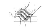
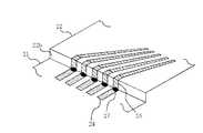
図1に示すように、画像表示素子は、ガラス板などからなる前面パネル1と、同じくガラス板などからなる前面パネル1に対向する裏面パネル2と、前面パネル1と裏面パネル2の間にマトリックス状に配置されて表示又は非表示の状態が選択される複数の画素(図示なし)と、この画素を制御する複数の電極(図示なし)とを有し、前面パネル1と裏面パネル2が画素及び電極を挟んで貼り合わされて構成されている。
裏面パネル2は、隣り合う複数の画素列の間でダイシングブレードを用いた切削加工(ダイシング加工)などによりV字形状を有する溝部3を形成して分割されている。
なお、図では判り易いように溝部3を拡大して表示しているが、実際は、溝部3は微小な隙間である。
また、画素はマトリックス状に配置されているので、「画素間」を言うときは、横方向の画素行列間と縦方向の画素列間が存在するが、両方を含めて「隣り合う2つの画素列」と称することとする。As shown in FIG. 1, the image display element includes a
The
In addition, although the
Also, since the pixels are arranged in a matrix, when referring to “between pixels”, there are between the pixel matrix in the horizontal direction and between the pixel columns in the vertical direction. It will be referred to as a “column”.
そして、溝部3に位置する前面パネル1側には、電極に繋がる複数の電極端子4が配置されている。電極端子4は、例えば、電極と同じ材料で同時に形成されたものであり、溝部3で露出させている。
一方、裏面パネル2の裏面2a(前面パネル1と対向する面の裏側)を「裏面」と称する。(以下同じ)
溝部3を構成する裏面パネル2の端部の端面(傾斜面)2bには、金属(例えば、Agなど)膜配線5が形成されている。裏面2a側の金属膜配線5の端部にコネクタ6を接続している。
このコネクタ6を介して金属膜配線5が外部の駆動回路に接続される。
なお、金属膜配線5の材料は、Agに限られるものではなく、一般的な配線材料を用いてもよい。また、金属膜配線5の配線方法にも特に制限はなく、金属膜配線5とコネクタ6の間にFPCなどの他の配線構造が含まれてもよい。A plurality of
On the other hand, the
A metal (for example, Ag)
The
The material of the
配線部の詳細を図2に示す。図のように、裏面パネル2を前面パネル1に貼り合わせた状態で、裏面パネル2の端部傾斜面2bの金属膜配線5が前面パネル1側の電極端子4に接触するように、電極端子4と金属膜配線5の位置を合わせて形成されている。
なお、電極端子4の溝部3で露出した部分は金属膜配線5で覆われており、これにより電極端子4に金属膜配線5が確実に接触している。
また、図1においても、各電極端子4の溝部3で露出した部分は、金属膜配線5で全面覆われている。
図1では、電極端子4の溝部3で露出した部分が、金属膜配線5で覆われていることを表すために、金属膜配線5の一部を切り欠いて示している。Details of the wiring section are shown in FIG. As shown in the drawing, in a state where the
In addition, the part exposed by the
Also in FIG. 1, the portions exposed at the
In FIG. 1, a part of the
裏面パネル2は、一般にガラスで構成されているため、金属膜配線5は、例えば銀(Ag)ペーストを用いて、厚膜印刷等によって塗布された後、焼成されて形成される。
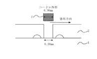
この場合、厚膜印刷等を行うために必要なニードルやヘッドなどの加工用の工具を裏面パネル2の端面2bに近接して移動させる必要である。
ここで、図3に示すように、裏面パネル2の端面2bがパネル面に垂直であり、例えば、溝部3の幅0.30mm、工具7の幅寸法が0.36mmのように、溝部3の幅が工具7の幅寸法より小さい場合には、厚膜印刷を適切に行うことが困難である。
これに対して、実施の形態1においては、裏面パネル2の分割部分に、前面パネル1の反対側となる上部が底部よりも幅広のV字形状を有する溝部3を形成しているので、図4に示すように、厚膜印刷等に必要な工具7を裏面パネル2の端面2bに近接させて移動することが可能であり、金属膜配線5を容易かつ正確に形成することができる。
なお、図2において、“g1”は溝部3の上部の幅、“g2”は底部の幅、“θ”は裏面パネル2の端部(端面)2bの傾斜角を示している。Since the
In this case, it is necessary to move a processing tool such as a needle or a head necessary for thick film printing or the like in the vicinity of the
Here, as shown in FIG. 3, the
On the other hand, in the first embodiment, in the divided portion of the
In FIG. 2, “g1” indicates the width of the upper portion of the
この発明は、図1、図2、図4に示したように、前面パネル1と、この前面パネル1に対向する裏面パネル2と、両パネル(即ち、前面パネル1及び裏面パネル2)間にマトリクス状に配置されて表示又は非表示の状態が選択される複数の画素と、この画素を制御するための複数の電極とを有し、両パネルが前記画素及び前記電極を挟んで貼り合わされて構成される画像表示素子において、裏面パネル2は、隣り合う複数の画素列の間で前面パネル1の反対側となる上部が底部より幅広の形状を有する溝部を形成するように分割され、溝部3に位置する端面(傾斜面2b)に沿って電極を駆動回路に接続する金属膜配線5を形成することにより、パネルの狭い領域から電極を引き出すことができるようになり、画像表示素子をマトリックス状に複数枚表示した時に、継ぎ目部の幅を狭くして、継ぎ目が目立たない高解像度の画像表示装置を実現できると共に、更に、金属膜配線そのものの信頼性向上や隣接する金属膜配線間あるいは電極端子間でのマイグレーション発生などを抑制できる高信頼度な画像表示装置を実現するものである。 As shown in FIGS. 1, 2, and 4, the present invention includes a
以上は、本発明による画像表示素子の基本的な構成とその効果を説明したものであるが、以下に、実施の形態1による画像表示素子の特徴的な具体例について説明する。
図5は、実施の形態1による画像表示素子の特徴的な構造を説明するための概念図であり、電極端子4と金属膜配線5を導電ペースト(例えば、Agペースト)10を塗布して接続する場合を示している。
図1に示した例では、コネクタ6を介して電極端子4を外部の駆動回路に接続する金属膜配線5は、電極端子4の端部と直接接続されるように、V型の溝部(即ち、前面パネル1の反対側となる上部が底部より幅広の形状を有する溝部)3を構成する傾斜面である「裏面パネル2の端部2b」の領域も含めて形成されている。
なお、この金属膜配線5は、前述したように、例えばAgペーストを厚膜に塗布した後に焼成されて形成されおり、各電極に対応して配置されている。The basic configuration of the image display device according to the present invention and the effects thereof have been described above. Specific examples of the image display device according to the first embodiment will be described below.
FIG. 5 is a conceptual diagram for explaining the characteristic structure of the image display element according to the first embodiment. The
In the example shown in FIG. 1, the
Note that, as described above, the
これに対して、図5では、V型の溝部3の底部に位置する電極端子4と裏面パネル2の裏面2aに形成されている金属膜配線5との間を導電ペースト(例えば、Agペースト)10を塗布して接続している。
なお、導電ペースト10は各電極端子4の上面に塗布されているが、この状態を表すために、図5では、導電ペースト10の一部を切り欠いて示している。
後掲する図8、図9、図11、図12において、同様の理由により、導電ペースト10の一部を切り欠いて示している。
また、図5では、金属膜配線5の端部と導電ペースト10の端部が当接して接続されているように描かれているが、実際には金属膜配線5の端部の上にまで導電ペースト10が塗布されている。このことは、後掲する図8、図9、図10、図11および図12においても同様である。
導電ペースト10による配線では、加工が容易になり、導電ペースト10の厚みの調整も容易である。
従って、電極端子4と金属膜配線5の接続部の性能(例えば、接続抵抗の均一化)や接続の信頼性が改善される。
更に、配線である導電ペースト10をカバーガラスである裏面パネル2の裏面2a及び端部(傾斜面)2bに密着させるので、耐震性や膨張・収縮に対する強度が改善される。On the other hand, in FIG. 5, a conductive paste (for example, Ag paste) is formed between the
In addition, although the electrically
In FIG. 8, FIG. 9, FIG. 11, and FIG. 12 to be described later, a part of the
Further, in FIG. 5, the end of the
In the wiring using the
Therefore, the performance (for example, uniform connection resistance) of the connection portion between the
Furthermore, since the
以上説明したように、本実施の形態による画像表示素子は、前面パネル1と、この前面パネル1に対向する裏面パネル2と、前面パネル1及び裏面パネル2間にマトリクス状に配置されて表示又は非表示の状態が選択される複数の画素と、この画素を制御する複数の電極とを有し、前面パネル1と裏面パネル2が画素及び電極を挟んで貼り合わされて構成され、金属膜配線5を介して電極を駆動回路に接続する画像表示素子において、
裏面パネル2は、隣り合う複数の画素列の間で電極に繋がる電極端子4が露出するように分割されると共に、この分割部分に前面パネル1との対向面の裏側にある上部が底部より幅広の形状を有する溝部3が形成されており、金属膜配線5は、裏面パネル2の上部の面(即ち、前面パネル1との対向面の裏側の面2a)に形成されており、電極端子4と金属膜配線5は、溝部3を構成する傾斜面に沿って塗布された導電ペースト10により接続されている。
これにより、パネルの狭い領域から電極を容易に引き出すことが可能となり、パネルの継ぎ目が目立たない高解像度の画像表示装置を容易に実現できると共に、更に、電極端子と金属膜配線との接続部の性能、信頼性、強度が改善される。As described above, the image display element according to the present embodiment is arranged in a matrix form between the
The
As a result, the electrodes can be easily drawn out from the narrow area of the panel, and a high-resolution image display device in which the joint of the panel is not conspicuous can be easily realized. Further, the connection portion between the electrode terminal and the metal film wiring can be easily realized. Performance, reliability and strength are improved.
なお、前述の説明では、裏面パネル2は、中央部で2分割されたものを想定しているが、分割数と分割位置はこれに限定されるものではない。裏面パネル2を3分割以上に分割してもよく、分割する位置も画素の間であれば他の位置であってもよい。
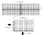
例えば、図6に示すように、裏面パネル2を十字状の溝部3により4分割し、画像表示素子の中央から電極を取出す中央取出し方式の構造にも適用できる。
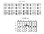
また、前面パネルの外周の端部から電極端子4を取出す場合や、図7に示すような画像表示素子の水平、垂直両端部から電極を取出す端部取出し方式の構造にも適用できる。
これは、後述する各実施の形態の画像表示素子においても同様である。In the above description, the
For example, as shown in FIG. 6, the
Further, the present invention can be applied to the case where the
The same applies to the image display elements of the embodiments described later.
実施の形態2.
図8は、実施の形態2による画像表示素子の特徴的な構造を説明するための概念図である。
本実施の形態は、図8に示すように、前掲した図5の構成において、更に、裏面パネル2の端部(傾斜面)2bの表面を荒らした(粗にした)ことを特徴とする。
なお、端部2bの表面は荒れていればよく、また、表面を荒らす方法は特に制限しないが、例えば、表面研削やサンドブラストなどの方法がある。また、表面の粗さは、例えば、砥石の粒度で規定される#2000〜#100程度である。
これにより、配線である導電ペースト10の裏面パネル2の端部(傾斜面)2bへの密着性が向上する。
更に、裏面パネル2の端部(傾斜面)2bの表面を荒らしたので、裏面パネル2の端部(傾斜面)2bでの配線(即ち、導電ペースト10)間の沿面距離が長くなり、マイグレーションの発生が抑制され、マイグレーション発生による短絡故障が軽減され、信頼性が改善される。
FIG. 8 is a conceptual diagram for explaining a characteristic structure of the image display element according to the second embodiment.
As shown in FIG. 8, the present embodiment is characterized in that the surface of the end (inclined surface) 2b of the
In addition, the surface of the
Thereby, the adhesiveness to the edge part (inclined surface) 2b of the
Furthermore, since the surface of the end (inclined surface) 2b of the
実施の形態3.
図9は、実施の形態3による画像表示素子の特徴的な構造を説明するための概念図である。
本実施の形態は、図9に示すように、実施の形態1における図5の構成において、隣接する導電ペースト10の間にディスペンサにて樹脂材を塗布して隔壁11を設けたことを特徴とする。
これにより、配線である導電ペースト10間の沿面距離が長くなり、マイグレーションなどによる短絡故障が軽減され、信頼性が改善される。
なお、隣接する電極端子の間にも樹脂材を塗布して隔壁を設けることにより、更にマイグレーションの発生は軽減される。
FIG. 9 is a conceptual diagram for explaining a characteristic structure of the image display element according to the third embodiment.
As shown in FIG. 9, the present embodiment is characterized in that the
As a result, the creepage distance between the
The occurrence of migration is further reduced by applying a resin material between adjacent electrode terminals to provide partition walls.
実施の形態4.
図10は、実施の形態4による画像表示素子の特徴的な構造を説明するための概念図である。
本実施の形態は、図10に示すように、前掲の図5の構成において、導電ペースト10を、複数本の導電ペースト(例えば、導電ペースト10a、10b、10cの3本の導電ペースト)で構成したことを特徴とする。
導電ペースト10を複数の導電ペーストで構成することにより、導電ペーストの塗布幅あるいは厚みを拡大することができる。
なお、図では、3本の導電ペースト10a、10b、10cは、互いに離れて形成されているが、これらは密着して形成されてもよい。
これにより導電ペースト10の電気抵抗を低減できると共に、電極端子と金属膜配線との接続部の信頼性が改善される。
FIG. 10 is a conceptual diagram for explaining a characteristic structure of the image display device according to the fourth embodiment.
In the present embodiment, as shown in FIG. 10, the
By forming the
In the figure, the three
Thereby, the electrical resistance of the
実施の形態5.
図11は、実施の形態5による画像表示素子の特徴的な構造を説明するための概念図である。
本実施の形態は、図11に示すように、電極端子4と金属膜配線5とを接続する導電性ペースト10は、溝部3を構成する2つの端部(傾斜面)2b、2b′において、交互に形成されている。
電極端子4は、溝部3の底部において、端部(傾斜面)2b及び2b′に対応して交互に配置されている。
即ち、裏面パネル2の端部(傾斜面)2bにおいて、隣接する導電ペースト10の間隔は、図5の場合と比較すると約2倍となっている。
従って、隣接する導電ペースト10の間隔が大きくなり、導電ペースト10の幅を広くして、配線部である導電ペースト10の電気抵抗を低減できる。
また、隣接する導電ペースト10間の沿面距離が長くなり、マイグレーションの発生が抑制され、配線間の絶縁信頼性が改善される。
FIG. 11 is a conceptual diagram for explaining a characteristic structure of the image display device according to the fifth embodiment.
In the present embodiment, as shown in FIG. 11, the
The
That is, the end portion of the
Thus, the spacing between adjacent
Further, the creepage distance between the
実施の形態6.
図12は、実施の形態6による画像表示素子の特徴的な構造を説明するための概念図である。
本実施の形態は、図12に示すように、導電ペースト10、該導電ペースト10に接続する電極端子4及び金属膜配線5が形成されている領域において、これらを保護するための保護コーティングを施したしたものである。図において、12は保護コーティングを示す。
これにより、塵埃等の付着やマイグレーションの発生が抑制され、接続の信頼性が改善される。
FIG. 12 is a conceptual diagram for explaining a characteristic structure of the image display element according to the sixth embodiment.
This embodiment, as shown in FIG. 12, electrically
Thereby, the adhesion of dust and the like and the occurrence of migration are suppressed, and the connection reliability is improved.
実施の形態7.
前述の実施の形態6では、導電ペースト10、該導電ペースト10に接続する電極端子4及び金属膜配線5が形成されている領域において、これらを保護するための保護コーティングを施したが、この保護コーティングとして硬化型接着剤を使用して、溝部3を硬化型接着剤で埋めてもよい。
これによって、塵埃等の付着やマイグレーションの発生が抑制されると共に、溝部3の部分に対するストレスの集中が緩和されるので、パネルの強度を増すことができる。Embodiment 7 FIG.
In the sixth embodiment described above, the
As a result, the adhesion of dust and the like and the occurrence of migration are suppressed, and the concentration of stress on the
実施の形態8.
本発明の大型ディスプレイの画像表示素子1における電極端子4と画素との関係を説明するために、画像表示素子の一例としてELディスプレイパネルを用いたケースを利用して以下に記載する。図1の画像表示素子をELディスプレイパネルで形成する例である。
なお、本発明の画像表示素子はこれに限定されるものではなく、液晶パネル、PDP等にも応用可能である。Embodiment 8 FIG.
In order to explain the relationship between the
The image display element of the present invention is not limited to this, and can be applied to a liquid crystal panel, a PDP, and the like.
前面パネル1上に画素pである有機EL素子を複数配列し、画素の発光/非発光を制御する(図6の画素pが一つの有機EL素子である)通常の有機EL素子は、ITO等の透明電極と、正孔輸送材層、発光層及び電子輸送層等からなる有機層と、反射電極(例えばAl等)が順次形成されて、発光層から光が透明電極を透過して、前面パネル1側から出射している。
電極端子4と透明電極および反射電極を電気的に接続させ、電極端子4を溝部3まで引き出している。
金属膜配線5を介して(透明電極および反射電極を)コネクタ6と電気的に接続させ、外部の駆動制御回路から有機EL素子の発光/非発光の制御信号が送られる。A plurality of organic EL elements that are pixels p are arranged on the
The
A control signal for light emission / non-light emission of the organic EL element is sent from the external drive control circuit by electrically connecting the
電極端子は、透明電極と同じITOで形成しても良く、抵抗を下げるためにAl、Cr、Ag等の低抵抗金属で形成しても良く、これらを積層して形成しても良い。
裏面パネル2は、前面パネル1と同様にガラスで形成し、裏面パネル2の有機EL素子と対向側にエッチングやサンドブラスト等で凹部を形成する。裏面パネル2の凹部の形成面と前面パネル1の有機EL素子形成面とを対向するように貼り合わせる。UV硬化接着剤等により前記両基板を封止接合し、前記凹部による封止空間には、水分等の有機EL素子の劣化因子から保護するため乾燥剤を設置する。The electrode terminal may be formed of the same ITO as the transparent electrode, may be formed of a low-resistance metal such as Al, Cr, or Ag in order to reduce the resistance, or may be formed by laminating these.
The
電極の引出し加工を容易に行えると共に、電極引出部におけるマイグレーションの発生を抑制できる画像表示素子の実現に有用である。 This is useful for realizing an image display element that can easily perform electrode drawing processing and can suppress the occurrence of migration in the electrode drawing portion.
1 前面パネル 2 裏面パネル
2a 裏面パネルの裏面(上部) 2b 端面(傾斜面)
3 溝部 4 電極端子
5 金属膜配線 7 工具
10 導電ペースト 11 隔壁
12 保護コーティング
DESCRIPTION OF
3
Claims (14)
Translated fromJapanese前記裏面パネルは、隣り合う複数の画素列の間で前記電極に繋がる電極端子が露出するように分割されると共に、この分割部分に前記前面パネルとの対向面の裏側にある上部が底部より幅広の形状を有する溝部が形成されており、
前記金属膜配線は、前記裏面パネルの前記前面パネルとの対向面の裏側の面に形成されており、
前記電極端子と前記金属膜配線は、前記溝部を構成する傾斜面に沿って塗布された導電ペーストにより接続されていることを特徴とする画像表示素子。A front panel, a back panel opposite to the front panel, a plurality of pixels arranged in a matrix between the front panel and the back panel and selected for display or non-display, and a plurality of pixels for controlling the pixels In an image display element having an electrode, the front panel and the back panel are bonded to each other with a pixel and an electrode interposed therebetween, and the electrode is connected to a drive circuit through a metal film wiring.
The back panel, together with the electrode terminals connected to the electrodes between a plurality of adjacent pixel lines are divided so as to expose the upper on the back of the facing surfaces of thefront panel in the divided portion from the bottom portion A groove having a wide shape is formed,
The metal film wires are formed on the back surface of the facing surfaces of thefront panel of the back panel,
The image display element, wherein the electrode terminal and the metal film wiring are connected by a conductive paste applied along an inclined surface constituting the groove.
ことを特徴とする請求項1に記載の画像表示素子。The conductiveDenpe paste an image display device according to claim 1, characterized in that the two inclined surfaces forming a groove are formed alternately.
前記裏面パネルを、隣り合う複数の画素列の間で前記電極に繋がる電極端子が露出するように分割すると共に、この分割部分に前記前面パネルとの対向面の裏側にある上部が底部より幅広の形状を有する溝部を形成する第1の工程と、
前記金属膜配線を、前記裏面パネルの前記前面パネルとの対向面の裏側の面に形成する第2の工程と、
前記電極端子と前記金属膜配線を、前記溝部を構成する傾斜面に沿って塗布された導電ペーストにより接続する第3の工程を有することを特徴とする画像表示素子の製造方法。A front panel, a back panel opposite to the front panel, a plurality of pixels arranged in a matrix between the front panel and the back panel and selected for display or non-display, and a plurality of pixels for controlling the pixels In the method for manufacturing an image display element, comprising an electrode, wherein the front panel and the back panel are bonded to each other with a pixel and an electrode interposed therebetween, and the electrode is connected to a drive circuit via a metal film wiring.
Said back panel, a plurality of electrode terminals connected to the electrodes between the adjacent pixel lines are divided so as to expose, wider than the upper bottom on the back of the facing surfaces of thefront panel to the divided portion A first step of forming a groove having the shape of
The metal film wires, and a second step of forming on the back surface of the facing surfaces of thefront panel of the back panel,
A method for manufacturing an image display element, comprising: a third step of connecting the electrode terminal and the metal film wiring with a conductive paste applied along an inclined surface constituting the groove.
Priority Applications (6)
| Application Number | Priority Date | Filing Date | Title |
|---|---|---|---|
| JP2009152432AJP5271170B2 (en) | 2009-06-26 | 2009-06-26 | Image display element and manufacturing method thereof |
| TW098144669ATWI416443B (en) | 2009-06-26 | 2009-12-24 | Portrait display element and method of manufacturing the same |
| KR1020100010003AKR101117420B1 (en) | 2009-06-26 | 2010-02-03 | Image display element and manufacturing method thereof |
| US12/700,299US8362362B2 (en) | 2009-06-26 | 2010-02-04 | Image display element with a divided back panel |
| EP10152580.6AEP2267517B1 (en) | 2009-06-26 | 2010-02-04 | Image display element and manufacturing method thereof |
| CN2010101195009ACN101930721A (en) | 2009-06-26 | 2010-02-05 | Image display element and manufacturing method thereof |
Applications Claiming Priority (1)
| Application Number | Priority Date | Filing Date | Title |
|---|---|---|---|
| JP2009152432AJP5271170B2 (en) | 2009-06-26 | 2009-06-26 | Image display element and manufacturing method thereof |
Publications (2)
| Publication Number | Publication Date |
|---|---|
| JP2011008092A JP2011008092A (en) | 2011-01-13 |
| JP5271170B2true JP5271170B2 (en) | 2013-08-21 |
Family
ID=42735802
Family Applications (1)
| Application Number | Title | Priority Date | Filing Date |
|---|---|---|---|
| JP2009152432AExpired - Fee RelatedJP5271170B2 (en) | 2009-06-26 | 2009-06-26 | Image display element and manufacturing method thereof |
Country Status (6)
| Country | Link |
|---|---|
| US (1) | US8362362B2 (en) |
| EP (1) | EP2267517B1 (en) |
| JP (1) | JP5271170B2 (en) |
| KR (1) | KR101117420B1 (en) |
| CN (1) | CN101930721A (en) |
| TW (1) | TWI416443B (en) |
Families Citing this family (7)
| Publication number | Priority date | Publication date | Assignee | Title |
|---|---|---|---|---|
| KR20150055188A (en)* | 2013-11-12 | 2015-05-21 | 삼성디스플레이 주식회사 | Display device and manufacturing method of the same |
| JP2015128863A (en)* | 2014-01-08 | 2015-07-16 | セイコーエプソン株式会社 | Wiring board, liquid droplet discharge head, printing device, electronic device, and wiring board manufacturing method |
| US11129469B2 (en) | 2018-03-19 | 2021-09-28 | Dongguan Shichang Metals Factory Ltd. | Collapsible brace member for a furniture support structure |
| CN109920762B (en) | 2019-03-28 | 2021-12-03 | 京东方科技集团股份有限公司 | Manufacturing method of array substrate, array substrate and display device |
| CN111653200B (en)* | 2020-06-29 | 2022-05-13 | 上海中航光电子有限公司 | Array substrate, display panel and display device |
| CN114696129A (en)* | 2020-12-28 | 2022-07-01 | 超聚变数字技术有限公司 | Display module and electronic equipment |
| CN112331714B (en)* | 2021-01-04 | 2021-04-23 | 京东方科技集团股份有限公司 | Display substrate and display device |
Family Cites Families (12)
| Publication number | Priority date | Publication date | Assignee | Title |
|---|---|---|---|---|
| JP3648337B2 (en)* | 1996-11-14 | 2005-05-18 | 株式会社東芝 | Active matrix liquid crystal display device |
| JP2000183470A (en)* | 1998-12-16 | 2000-06-30 | Sony Corp | Wiring where migration is prevented and its prevention method |
| US6567138B1 (en)* | 1999-02-15 | 2003-05-20 | Rainbow Displays, Inc. | Method for assembling a tiled, flat-panel microdisplay array having imperceptible seams |
| JP4345153B2 (en)* | 1999-09-27 | 2009-10-14 | ソニー株式会社 | Manufacturing method of video display device |
| JP4115065B2 (en)* | 2000-03-07 | 2008-07-09 | 三菱電機株式会社 | Image display element and image display device |
| JP2005134637A (en)* | 2003-10-30 | 2005-05-26 | Optrex Corp | Liquid crystal display |
| JP4614652B2 (en)* | 2003-11-27 | 2011-01-19 | 株式会社半導体エネルギー研究所 | Thin film transistor manufacturing method and display device manufacturing method |
| JP2005183106A (en)* | 2003-12-18 | 2005-07-07 | Mitsubishi Electric Corp | PM type organic EL panel |
| JP5023488B2 (en)* | 2005-03-09 | 2012-09-12 | セイコーエプソン株式会社 | Device mounting structure and device mounting method, droplet discharge head, drive unit, and semiconductor device |
| JP4939964B2 (en)* | 2007-02-06 | 2012-05-30 | 三菱電機株式会社 | Image display element |
| JP5089266B2 (en)* | 2007-06-26 | 2012-12-05 | 三菱電機株式会社 | Manufacturing method of image display element |
| JP2009109770A (en)* | 2007-10-30 | 2009-05-21 | Fujitsu Ltd | Display device manufacturing method and display device |
- 2009
- 2009-06-26JPJP2009152432Apatent/JP5271170B2/ennot_activeExpired - Fee Related
- 2009-12-24TWTW098144669Apatent/TWI416443B/ennot_activeIP Right Cessation
- 2010
- 2010-02-03KRKR1020100010003Apatent/KR101117420B1/ennot_activeExpired - Fee Related
- 2010-02-04EPEP10152580.6Apatent/EP2267517B1/ennot_activeNot-in-force
- 2010-02-04USUS12/700,299patent/US8362362B2/ennot_activeExpired - Fee Related
- 2010-02-05CNCN2010101195009Apatent/CN101930721A/enactivePending
Also Published As
| Publication number | Publication date |
|---|---|
| KR20110000488A (en) | 2011-01-03 |
| KR101117420B1 (en) | 2012-03-13 |
| US20100326708A1 (en) | 2010-12-30 |
| CN101930721A (en) | 2010-12-29 |
| TW201101262A (en) | 2011-01-01 |
| JP2011008092A (en) | 2011-01-13 |
| US8362362B2 (en) | 2013-01-29 |
| TWI416443B (en) | 2013-11-21 |
| EP2267517B1 (en) | 2015-07-01 |
| EP2267517A1 (en) | 2010-12-29 |
Similar Documents
| Publication | Publication Date | Title |
|---|---|---|
| JP5271170B2 (en) | Image display element and manufacturing method thereof | |
| CN101930699B (en) | Image display element and manufacturing method thereof | |
| JP5322805B2 (en) | Image display element and manufacturing method thereof | |
| CN101930695B (en) | Image display element and manufacturing method thereof | |
| TWI387945B (en) | Image display element manufacturing method | |
| TWI452552B (en) | Display device and method for manufacturing the same, and display |
Legal Events
| Date | Code | Title | Description |
|---|---|---|---|
| A621 | Written request for application examination | Free format text:JAPANESE INTERMEDIATE CODE: A621 Effective date:20120605 | |
| A977 | Report on retrieval | Free format text:JAPANESE INTERMEDIATE CODE: A971007 Effective date:20130207 | |
| A131 | Notification of reasons for refusal | Free format text:JAPANESE INTERMEDIATE CODE: A131 Effective date:20130219 | |
| A521 | Request for written amendment filed | Free format text:JAPANESE INTERMEDIATE CODE: A523 Effective date:20130326 | |
| TRDD | Decision of grant or rejection written | ||
| A01 | Written decision to grant a patent or to grant a registration (utility model) | Free format text:JAPANESE INTERMEDIATE CODE: A01 Effective date:20130416 | |
| A61 | First payment of annual fees (during grant procedure) | Free format text:JAPANESE INTERMEDIATE CODE: A61 Effective date:20130510 | |
| R150 | Certificate of patent or registration of utility model | Free format text:JAPANESE INTERMEDIATE CODE: R150 Ref document number:5271170 Country of ref document:JP Free format text:JAPANESE INTERMEDIATE CODE: R150 | |
| R250 | Receipt of annual fees | Free format text:JAPANESE INTERMEDIATE CODE: R250 | |
| R250 | Receipt of annual fees | Free format text:JAPANESE INTERMEDIATE CODE: R250 | |
| R250 | Receipt of annual fees | Free format text:JAPANESE INTERMEDIATE CODE: R250 | |
| R250 | Receipt of annual fees | Free format text:JAPANESE INTERMEDIATE CODE: R250 | |
| R250 | Receipt of annual fees | Free format text:JAPANESE INTERMEDIATE CODE: R250 | |
| R250 | Receipt of annual fees | Free format text:JAPANESE INTERMEDIATE CODE: R250 | |
| R250 | Receipt of annual fees | Free format text:JAPANESE INTERMEDIATE CODE: R250 | |
| LAPS | Cancellation because of no payment of annual fees |