JP5269799B2 - Wafer via formation - Google Patents
Wafer via formationDownload PDFInfo
- Publication number
- JP5269799B2 JP5269799B2JP2009533462AJP2009533462AJP5269799B2JP 5269799 B2JP5269799 B2JP 5269799B2JP 2009533462 AJP2009533462 AJP 2009533462AJP 2009533462 AJP2009533462 AJP 2009533462AJP 5269799 B2JP5269799 B2JP 5269799B2
- Authority
- JP
- Japan
- Prior art keywords
- groove
- wafer
- forming
- completed wafer
- back surface
- Prior art date
- Legal status (The legal status is an assumption and is not a legal conclusion. Google has not performed a legal analysis and makes no representation as to the accuracy of the status listed.)
- Expired - Fee Related
Links
- 230000015572biosynthetic processEffects0.000titleclaimsdescription13
- 238000000034methodMethods0.000claimsdescription113
- 238000000151depositionMethods0.000claimsdescription15
- 239000004020conductorSubstances0.000claimsdescription13
- 238000001312dry etchingMethods0.000claimsdescription4
- 238000005530etchingMethods0.000claimsdescription4
- 238000007747platingMethods0.000claimsdescription4
- 238000001039wet etchingMethods0.000claimsdescription4
- 235000012431wafersNutrition0.000description69
- 238000013459approachMethods0.000description14
- 239000010410layerSubstances0.000description13
- 238000010586diagramMethods0.000description10
- 239000002184metalSubstances0.000description9
- 230000008901benefitEffects0.000description7
- 239000004065semiconductorSubstances0.000description7
- 238000001465metallisationMethods0.000description6
- 239000012212insulatorSubstances0.000description5
- 230000008021depositionEffects0.000description4
- 239000000463materialSubstances0.000description2
- 230000004913activationEffects0.000description1
- 239000011248coating agentSubstances0.000description1
- 238000000576coating methodMethods0.000description1
- 230000008094contradictory effectEffects0.000description1
- 238000007796conventional methodMethods0.000description1
- 238000009713electroplatingMethods0.000description1
- 239000011229interlayerSubstances0.000description1
- 239000000758substrateSubstances0.000description1
- 239000011800void materialSubstances0.000description1
Images


Classifications
- H—ELECTRICITY
- H01—ELECTRIC ELEMENTS
- H01L—SEMICONDUCTOR DEVICES NOT COVERED BY CLASS H10
- H01L23/00—Details of semiconductor or other solid state devices
- H01L23/52—Arrangements for conducting electric current within the device in operation from one component to another, i.e. interconnections, e.g. wires, lead frames
- H—ELECTRICITY
- H01—ELECTRIC ELEMENTS
- H01L—SEMICONDUCTOR DEVICES NOT COVERED BY CLASS H10
- H01L21/00—Processes or apparatus adapted for the manufacture or treatment of semiconductor or solid state devices or of parts thereof
- H01L21/70—Manufacture or treatment of devices consisting of a plurality of solid state components formed in or on a common substrate or of parts thereof; Manufacture of integrated circuit devices or of parts thereof
- H01L21/71—Manufacture of specific parts of devices defined in group H01L21/70
- H01L21/768—Applying interconnections to be used for carrying current between separate components within a device comprising conductors and dielectrics
- H01L21/76898—Applying interconnections to be used for carrying current between separate components within a device comprising conductors and dielectrics formed through a semiconductor substrate
- H—ELECTRICITY
- H01—ELECTRIC ELEMENTS
- H01L—SEMICONDUCTOR DEVICES NOT COVERED BY CLASS H10
- H01L21/00—Processes or apparatus adapted for the manufacture or treatment of semiconductor or solid state devices or of parts thereof
- H01L21/70—Manufacture or treatment of devices consisting of a plurality of solid state components formed in or on a common substrate or of parts thereof; Manufacture of integrated circuit devices or of parts thereof
- H01L21/71—Manufacture of specific parts of devices defined in group H01L21/70
- H01L21/768—Applying interconnections to be used for carrying current between separate components within a device comprising conductors and dielectrics
Landscapes
- Engineering & Computer Science (AREA)
- Physics & Mathematics (AREA)
- Condensed Matter Physics & Semiconductors (AREA)
- General Physics & Mathematics (AREA)
- Computer Hardware Design (AREA)
- Microelectronics & Electronic Packaging (AREA)
- Power Engineering (AREA)
- Manufacturing & Machinery (AREA)
- Internal Circuitry In Semiconductor Integrated Circuit Devices (AREA)
- Electroplating Methods And Accessories (AREA)
Description
Translated fromJapanese[関連出願の相互参照]
本願は、35USC119(e)(l)を根拠とした、米国仮特許出願第60/829,772号に基づく優先権の利益を請求するものであり、その全文を参照することで本明細書に組み込む。[Cross-reference of related applications]
This application claims the benefit of priority under US Provisional Patent Application No. 60 / 829,772, based on 35 USC 119 (e) (l), and is incorporated herein by reference in its entirety. Include.
半導体ウエハを扱う場合、プロセス中に割れることがないよう厚いウエハを扱うことが好ましい。しかし、バイアが深くなるにつれて、その中に現在の堆積技法を利用してシード層を形成するのは、特にコストの点からみて次第に困難になっている。細いバイア内で、150μmを超える深さまでシード層を被覆するのは一般に困難であり、費用対効果が低下するのが普通である。従って、細い径のバイアを充填するのにめっき法を用いる場合、ほとんどの市販ウエハに共通している約500〜750μmが代表値(またはそれ以上)の厚さのウエハを最初に薄くすることなく、ウエハ上に上記特許出願のバイアを用いるのは困難である。しかしながら、このようなウエハを適切な厚さまで薄くすると、ウエハを曲げやすくすることができるが、ウエハは脆いので、取扱い中に割れる可能性が極めて高くなる。これはプロセス前のウエハでは許容できるリスクかもしれないが、コストを最小限に抑える場合、全プロセスが完了したウエハ(すなわち、少なくともフロントエンドプロセスを既に行ったもの、さらに多くの場合には、バックエンドプロセスをも行ったもの)ではコストが著しく高くなるので許容されない。 When handling semiconductor wafers, it is preferable to handle thick wafers so that they do not break during the process. However, as the vias become deeper, it becomes increasingly difficult to form a seed layer therein using current deposition techniques, particularly in terms of cost. It is generally difficult to coat the seed layer to a depth in excess of 150 μm in a narrow via and it is usually less cost effective. Therefore, when plating is used to fill narrow diameter vias, approximately 500-750 μm, which is common to most commercially available wafers, is made without first thinning a wafer with a typical (or greater) thickness. It is difficult to use the above patent application vias on the wafer. However, thinning such a wafer to an appropriate thickness can make the wafer easier to bend, but the wafer is fragile and therefore very likely to break during handling. This may be an acceptable risk for pre-process wafers, but to keep costs to a minimum, a wafer that has been fully processed (i.e., at least a front-end process has already been performed, and more often a back-end process) In the case of an end process), the cost is remarkably high and is not allowed.
本発明者らは、壊れやすい厚さまでウエハを薄くすることなく、全プロセス完了ウエハで上記参照のバイアが使用できるような、上記課題を解決する方法を発明した。更に本発明者らの手法は、極端に高精度の技法や高コストの技法を使用しなくても実行できるものである。 The inventors have invented a method that solves the above problems so that the above-referenced vias can be used on all process completed wafers without thinning the wafer to a fragile thickness. Furthermore, our technique can be implemented without using extremely high precision techniques or high cost techniques.
本発明者らの手法では、ウエハの選択部分の厚さだけを薄くする。この方法では、薄くした領域内の厚さは、上記参照のバイア手法を用いて適切なシード層を堆積できるような厚さである。更に、その領域部分だけを薄くするので、ウエハ全体の構造的な剛性を、必要とされる取扱いができる程度に保つことができる。更に、薄くする領域はバイアが配置される領域に限定することができ、その境界自体は厳密に決定されるものではないので、必要に応じて粗いエッチング技法を用いて広めにエッチングすることができる。実際、バイア形成後の薄くする加工でその境界全体を除去する場合がある。 In our approach, only the thickness of the selected portion of the wafer is reduced. In this method, the thickness in the thinned region is such that a suitable seed layer can be deposited using the via technique referenced above. Furthermore, since only the region portion is thinned, the structural rigidity of the entire wafer can be maintained to such an extent that it can be handled as required. Furthermore, the thinning region can be limited to the region where the via is located, and the boundary itself is not strictly determined, so that it can be etched extensively using a rough etching technique if necessary. . In fact, the entire boundary may be removed by thinning after forming the via.
全プロセス完了ウエハに導電性バイアを形成する手法の一実施の形態は、全プロセス完了ウエハの背面に少なくとも一つの溝領域を画成するステップと、その溝領域内に少なくとも一つの溝を、その溝内に形成されるバイアに対して全長にわたってシード被覆を可能にする、全体的な深さまで形成するステップと、全プロセス完了ウエハの溝内に所定の深さまでバイアを形成するステップと、バイアの全長にわたってシード層を堆積するステップと、導電性メタルでバイアを充填するためにシード層をめっきするステップとを含む。 One embodiment of a technique for forming conductive vias in an all process completed wafer includes defining at least one groove region on a back side of the entire process completed wafer, and including at least one groove in the groove region. Forming to an overall depth to allow seed coating over the entire length of the via formed in the groove; forming a via to a predetermined depth in the groove of the entire process completed wafer; and Depositing a seed layer over the entire length and plating the seed layer to fill the via with conductive metal.
本明細書に記載された利点および特徴は、代表的な実施例から得られる多くの利点および特徴のうちの数点であり、本発明の理解を助けるためだけに示されている。これらは、発明の限定または均等物の限定にはあたらないと解されるべきものである。たとえば、これらの利点のいくつかは、単一の実施例において同時に存在できないという点で、相互に矛盾したものである。同様に、いくつかの利点は、本発明の一態様に適用できるが、他の態様に適用できるものではない。さらなる特徴および利点は、以下の記載および図により明らかになるだろう。 The advantages and features described herein are just a few of the many advantages and features that can be gained from the exemplary embodiments and are presented only to assist in understanding the present invention. These should not be construed as limiting the invention or the equivalents. For example, some of these advantages are mutually contradictory in that they cannot exist simultaneously in a single embodiment. Similarly, some advantages are applicable to one aspect of the invention, but not to other aspects. Further features and advantages will become apparent from the following description and drawings.
米国特許出願第11/329,481号、第11/329,506号、第11/329,539号、第11/329,540号、第11/329,556号、第11/329,557号、第11/329,558号、第11/329,574号、第11/329,575号、第11/329,576号、第11/329,873号、第11/329,874号、第11/329,875号、第11/329,883号、第11/329,885号、第11/329,886号、第11/329,887号、第11/329,952号、第11/329,953号、第11/329,955号、第11/330,011号、および第11/422,551号には、半導体ウエハに小径、かつ深いバイアを形成するための各種の技法が記載されている。これらの出願の内容は、参照することにより全内容が本明細書に記述されているかのように組み込まれる。 No. 11 / 329,481, 11 / 329,506, 11 / 329,539, 11 / 329,540, 11 / 329,556, 11 / 329,557 11 / 329,558, 11 / 329,574, 11 / 329,575, 11 / 329,576, 11 / 329,873, 11 / 329,874, 11 / 329,875, 11 / 329,883, 11 / 329,885, 11 / 329,886, 11 / 329,887, 11 / 329,952, 11/329 Nos. 329,953, 11 / 329,955, 11 / 330,011, and 11 / 422,551 describe various techniques for forming small diameter and deep vias in semiconductor wafers. Been That. The contents of these applications are hereby incorporated by reference as if set forth in full herein.
これらの出願に記載された本発明者らの技法により、従来は到達できなかったバイアの密度および配置が可能になり、しかもチップ、ダイまたはウエハスケールで実行することができる。場合により、既にデバイスを形成したウエハ、バックエンドプロセス(すなわち、デバイス間接続、メタライズ層間接続の形成)を完了させたウエハ、または事前に薄くしていないウエハに本技法を実行することが望ましい。典型的な半導体ウエハは、厚さが約500μm〜750μmまたはそれ以上である。 Our techniques described in these applications allow via densities and placements that were not previously reachable and can be performed on a chip, die or wafer scale. In some cases, it may be desirable to perform this technique on wafers that have already had devices formed on them, wafers that have completed back-end processes (ie, formation of device-to-device connections, metallized interlayer connections), or wafers that have not been previously thinned. A typical semiconductor wafer has a thickness of about 500 μm to 750 μm or more.
しかしながら、上記のように、この厚さのウエハでは、デバイス接点または一つ以上のバックエンドメタライズ層まで達することができ、かつメタル化できるようにシード被覆が可能な、多数の、かつ小径の高密度バイアを作成するのは極めて困難である。上記参照の特許出願に記載されている手法は、ウエハスケールの手法を使用する場合の、バイア形成前にウエハを事前に薄くすることによって起こる問題にあまり触れていない。しかし、上記のように特定量を超えてウエハ全体を薄くすると、ルーチン的なウエハプロセス手法を用いる取扱いに対して壊れやすくなりすぎる。 However, as noted above, wafers of this thickness can reach device contacts or one or more back-end metallization layers, and can be seeded so that they can be metallized, with a large number of small diameter high Creating a density via is extremely difficult. The approach described in the above referenced patent application does not address much of the problems caused by pre-thinning the wafer prior to via formation when using a wafer scale approach. However, if the entire wafer is thinned beyond a certain amount as described above, it becomes too fragile for handling using routine wafer process techniques.
本発明者らの手法は「溝」技法であり、この技法には完全に形成済みのウエハの背面の第1エッチング領域が含まれる。これらの領域においてウエハを薄くするものである。これらの領域は、適切なシード層堆積が可能な、深いバイアの形成のために、薄くすることが必要となる。その一方で、ウエハの大部分は、全厚さのままであるか、あるいは事前に薄くした厚さであって、そのあとのウエハのルーチン的取扱いが可能な厚さおよび全体剛性を維持するような、厚さのままである。 Our approach is a “groove” technique, which includes a first etched region on the back of a fully formed wafer. In these regions, the wafer is thinned. These regions need to be thinned for the formation of deep vias that allow proper seed layer deposition. On the other hand, the majority of wafers remain in full thickness or have been pre-thinned to maintain a thickness and overall stiffness that allows for subsequent routine handling of the wafer. The thickness remains the same.
特定の実施の形態に応じて、薄くする領域は:i)ダイシングしたあとに得られる個々のチップの領域と同等またはそれ以上の領域を対象とするか;ii)バイアのグループが形成される狭い領域を対象とするか;またはiii)個々のバイアが形成される個々の領域だけを対象とすることができる。 Depending on the particular embodiment, the area to be thinned is: i) covers an area equal to or greater than the area of the individual chip obtained after dicing; ii) a narrow group in which via groups are formed Or iii) can only target individual regions where individual vias are formed.
用語統一のために、この薄くした領域を本明細書では、「溝」と称するが、言うまでもなく、この用語に、何れかの、特定形状、アスペクト比(すなわち、幅に対する深さの比)関係、または他の幾何構成を含ませる意図はない。 For the purpose of terminology, this thinned region is referred to herein as a “groove”, but it should be understood that this term has any specific shape, aspect ratio (ie, ratio of depth to width) relationship. Or any other geometric configuration is not intended.
更に、これらの溝は、詳細に後述する後続ステップで役立つように作成することができる。 In addition, these grooves can be created to be useful in subsequent steps described in detail below.
上記三つの手法のどれを用いたとしても、溝の全面積はウエハ全面積に対する割合で、普通は75%未満、典型的には50%以下として、ウエハの構造的完全性および従来の方法による取扱い方が確実に維持されるようにする。 Regardless of which of the above three approaches, the total groove area is a percentage of the total wafer area, usually less than 75%, typically 50% or less, depending on the structural integrity of the wafer and conventional methods. Ensure that handling is maintained.
有利な点は、この溝がバイアを形成するために用いるのと同一のエッチングプロセスで形成できるということにある。代替として、溝をウェットエッチングプロセスのような低精度のプロセスを用いて形成してもよい。 The advantage is that this groove can be formed by the same etching process used to form the via. Alternatively, the trench may be formed using a low precision process such as a wet etch process.
更に、溝の深さは、バイアの直径と深さに応じて深くても浅くてもよい。注意点として、必要な溝の深さは、溝の範囲内でウエハに形成されるバイアに対して、全深さまでシード層被覆可能となるような深さであることである。例えば、全厚さが750μmのウエハに直径50μmのバイアを作成するとしたら、要求される領域内のウエハ厚さが400μmとなる溝があればよく、あるいは直径10μmのバイアを作製するとしたらウエハ厚さが150μmとなる溝があればよい。先に注記したように、溝の範囲内でウエハが薄くなるほど、残すべき領域であるウエハに残存する領域が増加するが、より深い溝(すなわち、より薄いウエハの領域)を提供することもできる。 Furthermore, the depth of the groove may be deep or shallow depending on the diameter and depth of the via. It should be noted that the necessary groove depth is such that the seed layer can be covered to the full depth with respect to the via formed in the wafer within the groove. For example, if a via with a diameter of 50 μm is to be created on a wafer with a total thickness of 750 μm, it is sufficient if there is a groove with a wafer thickness of 400 μm in the required area, or if a via with a diameter of 10 μm is to be produced, the wafer thickness It is sufficient if there is a groove with a thickness of 150 μm. As noted above, the thinner the wafer within the groove, the more area left on the wafer that is to remain, but it can also provide a deeper groove (ie, a thinner wafer area). .
場合によっては、最も細いバイアでの場合が典型的であるが、二以上の「スタックされた溝」が使用される多段手法が、全体の構造的完全性を保ったまま必要な厚さまでウエハを薄くするために用いられ得る。 In some cases, the thinnest via is typical, but a multi-step approach where two or more “stacked grooves” are used can reduce the wafer to the required thickness while maintaining overall structural integrity. Can be used for thinning.
最後に、上記参照の、同一出願人による特許出願に記載されているようなバイアについて本手法を図解したが、同一の手法は、類似の課題をもつ他のバイア形成技法と併せて用いることも可能である。 Finally, although this approach is illustrated for vias as described in the above referenced patent application by the same applicant, the same approach can be used in conjunction with other via formation techniques with similar challenges. Is possible.
図に戻って、図1A〜図1Gに「溝」技法の一実施例の手法を略図で示す。 Returning to the figures, the technique of one embodiment of the “groove” technique is schematically illustrated in FIGS. 1A-1G.
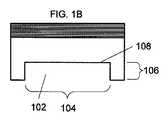
図1Aに半導体ウエハ100の一部を略図で示す。図示のように、半導体は、全厚さのままであり、ダイシングのための準備が済んでおり、フロントエンドプロセスおよびバックエンドプロセスが完了した状態である。但し、本実施例で本発明者らが想定しているのは、ウエハに、背面下から、バックエンドプロセスの一部として配置されたメタライズ層のうちの一層の一部にバイアを追加するというものである。 FIG. 1A schematically shows a part of a
プロセスは、以下のように進行する。 The process proceeds as follows.
最初に図1Bに示すように、深いメタル充填バイアが予定される領域に渡って溝102を形成するが、ウエハが厚すぎて、要求される深さまでのエッチング、シード堆積、またはその両方が不可能である。溝領域104は、例えば、従来のドライエッチングまたはウェットエッチング技法を用いて、バイア形成およびメタル化ポイント110までのシード堆積に必要な基準を満たすように、また(この例での)接続されるメタル化ポイント110から十分な深さである、深さ106まで、画成および形成され、新規の外表面108を画成する。 Initially, as shown in FIG. 1B,
注目すべきは、溝102の表面形状はそれを画成する能力だけで決まるという点である。従って、特定の用途に応じて、単純な四角形や円形から極めて複雑な幾何形状まで、任意の形状を用いることができる。 It should be noted that the surface shape of the
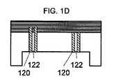
次に、所望の方法でバイアを形成する。図1C〜図1Gに示すように、説明のために、上記参照の特許出願に記載されているような環状バイアの手法を用いる。 Next, a via is formed by a desired method. As shown in FIGS. 1C-1G, for purposes of explanation, an annular via approach as described in the above referenced patent application is used.
簡明な説明のために、溝102内の二つのバイア110、112を示す。理解を容易にするために、左側のバイア110はメタライズ層内の中間点111まで延び、一方、右側のバイア112は最初のメタライズ層116までしか延びていない。言うまでもないが、バイア110、112は深さが異なるので、同時には形成されないが、バイアの深さが共通し直径が同一なら同時に作成される。更に言うまでもなく、図示の環状バイア110、112は正しい縮尺ではなく、大幅に誇張してあるので尺度は実情を反映していない。 For the sake of simplicity, two
図に戻ると、図1Cに示すように、環状リング形のバイア溝118が形成される。図1Dに示すように、バイア溝118は、絶縁体120で充填される。図1Eに示すように、絶縁体120内部の半導体材料の内側アイランド122は除去される。図1Fに示すように、シード層124が堆積されて、バイアは、この例では、電気めっきプロセスを用いてメタル126で充填される。そのあと、本プロセスの理解には無関係なデバイスパッドの形成やその他の所望の追加プロセスのステップが実行される。 Returning to the figure, as shown in FIG. 1C, an annular ring-shaped via
最後に、図1G、図1Hに示すように、使用される溝の量に応じて(すなわち、溝がチップの境界を超える単一の溝であったかどうか)、ウエハを、ソー切断もしくは(前の例での)ダイシングのいずれかで単に加工するか、またはメタル充填バイアにより形成される接点128、130にアクセスできるよう薄く加工してから、ダイシングもしくはソー切断することができる。どちらの場合も、薄くする手法に応じて、いくつかの実施の形態の変形形態では、新規形成バイアがポスト132、134として用いられ、他の実施の形態の変形形態では、バイアは取り付けられた接点パッド128、130を備えることができる。 Finally, as shown in FIGS. 1G and 1H, depending on the amount of grooves used (ie, whether the grooves were a single groove beyond the chip boundary), the wafer was saw cut or (previous Either by dicing (in the example) can be simply processed, or thinned to access
注意すべきは、本手法を一対のバイアとして説明したが、本手法は、単一バイアでも多数バイア(二つから文字通り数百以上まで)でも同一であり、唯一、使用する溝のサイズまたは形状が異なるだけである。 It should be noted that although the method has been described as a pair of vias, the method can be the same for a single via or multiple vias (from two to literally more than a few hundred), and only the size or shape of the groove used. Is only different.
図2に本明細書で説明するような一実施例の手法を用いるウエハ200を、溝のある面と(図2A)、A−Aに沿った断面(図2B)の両方の略図で示す。本手法では、溝202は、ウエハ200上に形成される個々のチップ204と整列し、かつ僅かに大きくなるようなサイズおよび形状としている。 FIG. 2 shows a schematic of a
図3A〜図3Lに、例えば、厚いウエハに極端に細いバイアまたは特定の接点形成要件に適合する、二以上の「スタックされた」溝を含む上記手法の変形を示す。 3A-3L illustrate a variation of the above approach that includes two or more “stacked” grooves, for example, to fit extremely thin vias or specific contact formation requirements on a thick wafer.
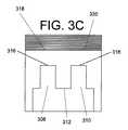
上記手法と同様に、本手法は、完全に形成済みのウエハ300で開始する。図3Aに簡略化した部分を示す。 Similar to the above technique, the technique starts with a fully formed
図3Bに示すように、溝302は、ウエハ300の背面304に規定の深さ306まで、上記と同様に、例えば、ウェットエッチングまたはドライエッチング手法を用いて形成される。 As shown in FIG. 3B, the
次に、図3Cに示すように、第1の溝302の形成と同一方法で、一対の小さな溝308、310が第1の溝302の底面312に形成される。誤解されないように注意しておくと、「同一方法」の意味は、第1の溝302の下面312が開始面として(すなわち、第1の溝302が形成される前のウエハ300の元の面314のように)扱われるということである。第1の溝を形成するために用いたのと同一の手法を必ずしも使用する必要はなく、同一手法でも異なる手法でもよい。 Next, as shown in FIG. 3C, a pair of
第2の深さの溝308、310を形成後、第2の溝308、310の底面316と、所望する接続点318、320との間の距離は、意図するバイアサイズでのシード堆積が可能となるのに必要な範囲内になる。 After forming the
これで、実際のバイア形成プロセスを開始でき、簡明な例示のために、基本的な環状バイアの手法を用いる(上記したように寸法は正しい縮尺ではないことに留意)。従って、図3Dに示すように、環状バイア322、324は、第2の溝308、310の底面316から、さらにメタライズ層のそれぞれのポイントである、それぞれ所望する接続点318、320まで延びるように作成される。 Now the actual via formation process can be started, and for the sake of conciseness, use the basic annular via approach (note that the dimensions are not to scale as noted above). Thus, as shown in FIG. 3D, the
ここで、注目すべきは、二つの異なる溝302、308を用いて適切な深さをウエハ基盤上に構築するが、大部分のウエハの厚さが、接続点318までの厚さNのままで元の面314に残るということである。更にウエハ300の広い部分がN−Zの厚さで残り、ウエハの狭い部分だけがN−(Y+Z)の厚さとなる。更に、この多重深さ(または多段)の手法を用いると、ウエハが弱くなるという重大なリスクを招くことなく、深さYとZを選択する自由度が得られる。 Here, it should be noted that an appropriate depth is constructed on the wafer substrate using two
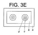
図3Eに溝側からみたウエハ300の部分図を示す。従って、図3Eは、面「a」、「b」、「c」および環状溝「d」の別の図を示す。 FIG. 3E shows a partial view of the
図3Fに、環状バイア322、324が絶縁体326により充填されたあとのウエハ300を示す。図3Gに、環状絶縁体326内部の半導体材料のアイランド328を、所望のメタル接続点318、320まで除去したあとのウエハ300を示す。図3Hに、ボイドにシード加工322してメタル324で充填したあとのウエハ300を示す。 FIG. 3F shows the
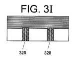
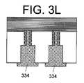
この時点で、本手法により、二つの新規オプションが利用可能になる。一つのオプションでは、図3Iに示すように、ウエハ300をダイシングして、そのチップを薄くして新規に形成される接点326、328を露出させるか、またはウエハ300を薄くしてからダイシングすることができる。どちらの場合でもその後、要望または必要があれば、例えば、接点パッド330、332を作成する(図3J)。他のオプションでは、例えば、全体的なバイアのピッチや第2の溝が適切なサイズと空間であるのとは対照的に、非常に細いバイアを必要とする理由が接続されるポイントに関係している場合、ウエハまたは(ダイシングされている場合は)チップは、第2バイアまで簡単に薄くすることができる(図3K)。その後、図3Lに示すように、接点パッド形成プロセスの前に、またはそのプロセスの一部として、第2バイアを導体334で充填することができる。この方法で、ウエハまたはチップをより厚く維持することができる。 At this point, the method makes two new options available. In one option, as shown in FIG. 3I,
図4は、上記手法の内の一つを用いて作成されたウエハの一部の写真である。写真から分かるように、図4の手法の場合、多数の溝が単一チップの境界内で用いられている。この例では、個々のバイアを基準として用いられている。 FIG. 4 is a photograph of a portion of a wafer created using one of the above techniques. As can be seen from the photograph, in the case of the technique of FIG. 4, a number of grooves are used within the boundaries of a single chip. In this example, individual vias are used as a reference.
最後に、注目に値するのは、幾つかの変形形態で、他の目的に役立てるための溝も形成できるということである。例えば、多様な実施の形態においては、環状溝内のチャネル絶縁体に役立てるか、または経路変更配線となるメタル、でなければ経路変更配線を形成するメタルを閉じ込めるように、溝を設計できる。このように、特定の実施の形態および構成に応じて、上記説明のバイア深さの問題に対処するだけでなく多目的の溝として役立てることができる。 Finally, it is noteworthy that in some variations, grooves can also be formed to serve other purposes. For example, in various embodiments, the groove can be designed to confine the metal that serves as the channel insulator in the annular groove, or otherwise forms the path change wiring, or otherwise the metal that forms the path change wiring. Thus, depending on the particular embodiment and configuration, it can serve as a multipurpose groove as well as address the via depth problem described above.
このように、ここでの記載(図含む)は、説明に役立つ代表的な実施例にすぎないと解されるべきである。読み手の便宜のため、上記記載は、あらゆる可能な実施例のうちの代表的な例に専心したものである。例は、本発明の原理を教授する。上記記載は、包括的にあらゆる可能な変形例を列挙しているわけではない。このような代替の実施例は、本発明の特定の部分のためには提示されていないかもしれない、もしくは、さらに不記載の代替の実施例が、(本発明の特定の)部分のためには有用であるかもしれないが、これらの代替の実施例についての権利の放棄とみなされるものではない。当業者は、こうした不記載の実施例の多くが、本発明および他の均等物の原理と同一の原理を包含していることを認識するであろう。 Thus, the description herein (including the figures) is to be understood as being merely representative examples useful for illustration. For the convenience of the reader, the above description is devoted to a representative example of all possible embodiments. The examples teach the principles of the present invention. The above description is not exhaustive of all possible variations. Such alternative embodiments may not be presented for specific parts of the invention, or further alternative embodiments not described for (particular) parts of the invention. May be useful, but is not considered a waiver of these alternative embodiments. Those skilled in the art will recognize that many of these undescribed embodiments encompass the same principles as the principles of the present invention and other equivalents.
Claims (16)
Translated fromJapanese前記プロセス完了ウエハの前記背面に、第1の溝を形成するステップと;
前記第1の溝の底面に、断面積を有する第2の溝を形成するステップと;
前記プロセス完了ウエハの前記背面に、前記第2の溝の底面から前記プロセス完了ウエハの前記背面に第1の所定の深さまで伸びるバイアを形成するステップであって、前記バイアは、前記第2の溝の前記断面積より小さい断面積を有する、ステップと;
前記第1の所定の深さと前記第2の溝の前記底面との間に、前記バイアの全長にわたってシード層を堆積するステップと;
導電性材料で前記バイアを充填するために前記シード層をめっきするステップと;
少なくとも前記第2の溝を形成するステップの後に、前記プロセス完了ウエハの前記背面を薄くするステップと;
前記プロセス完了ウエハの前記背面を薄くするステップの後に、前記第2の溝内に導体を堆積するステップと;
を備え、
前記第1の溝を形成するステップまたは前記第2の溝を形成するステップの少なくとも1つは、ウェットエッチングまたはドライエッチングの少なくとも1つを用いて、前記プロセス完了ウエハの前記背面をエッチングするステップを含む、方法。A method of forming conductive vias on a process completed wafer, the method comprising:
Forming a first groove in the back surface of the process-completed wafer;
Forming a second groove having a cross-sectional area on the bottom surface of the first groove;
Forming a via on the back surface of the process-completed wafer from a bottom surface of the second groove to a first predetermined depth on the back surface of the process-completed wafer; Having a cross-sectional area smaller than the cross-sectional area of the groove;
Depositing a seed layer over the entire length of the via between the first predetermined depth and the bottom surface of the second groove;
Plating the seed layer to fill the via with a conductive material;
Thinning the backside of the process-completed wafer after at least the step of forming the second groove;
Depositing conductors in the second trenches after thinning the backside of the process-completed wafer;
With
At least one of forming the first groove or forming the second groove comprises etching the back surface of the process-completed wafer using at least one of wet etching or dry etching. Including.
前記複数の第1の溝は、溝領域を画成し、
前記溝領域は、前記プロセス完了ウエハの前記背面の領域全面積の75%未満である、
請求項1の方法。Forming a plurality ofthe first grooves onthe back surface of the process-completed wafer;
The plurality offirst grooves define a groove region;
The groove region is less than 75% of the total area of the back region of the process-completed wafer;
The method of claim 1.
請求項2の方法。The groove region is less than 50% of the total area of the region of the back surface of the process-completed wafer;
The method of claim 2.
前記方法は、前記複数のチップのうちの1つ以上の外側の境界を超える前記第1の溝のための外縁を画成するステップを更に備える、
請求項1の方法。The process completion wafer comprises a plurality of chips,
The method further comprises defining an outer edge forthe first groove beyond one or more outer boundaries of the plurality of chips.
The method of claim 1.
前記方法は、少なくとも部分的に、前記複数のチップのうちの1つの外側の境界の内部にある前記第1の溝のための外縁を画成するステップを更に備える、
請求項1の方法。The process completion wafer comprises a plurality of chips,
The method further comprises defining an outer edge forthe first groove that is at least partially within an outer boundary of one of the plurality of chips.
The method of claim 1.
前記方法は、前記複数のチップのうちの1つと実質的に整列する前記第1の溝を画成するステップを更に備え;
前記第1の溝は、前記複数のチップのうちの前記1つより僅かに大きいサイズを有する、
請求項1の方法。The process completion wafer comprises a plurality of chips,
The method furthercomprises definingthe first groove substantially aligned with one of the plurality of chips;
The first groove has a size slightly larger than the one of the plurality of chips;
The method of claim 1.
請求項1の方法。After the step of depositing a conductor in the second groove, further comprising sawing or dicing a chip from the process-completed wafer;
The method of claim 1.
請求項1の方法。The first groove has an outer edge boundary defining a first groove region, and the second groove is formed in the first groove region;
The method of claim 1.
請求項8の方法。Forming the via includes forming the via in an outer edge boundary of the second groove;
The method of claim8 .
前記プロセス完了ウエハの背面から第1の溝を形成するステップであって、前記第1の溝は、部分的に前記プロセス完了ウエハ内に形成され、前記プロセス完了ウエハの前記背面は薄くされていない、ステップと;
前記第1の溝の底面から第1の所定の深さまで、断面積を有する第2の溝を形成するステップと;
前記第2の溝の底面から前記プロセス前記プロセス完了ウエハの前記背面に第2の所定の深さまでバイアを形成するステップであって、前記バイアは、前記第2の溝の断面積より小さい断面積を有する、ステップと;
前記第2の所定の深さと前記第2の溝の前記底面との間に、前記バイアの全長にわたってシード層を堆積するステップと;
導電性材料で前記バイアを充填するために前記シード層をめっきするステップと;
少なくとも前記第2の溝を形成するステップの後に、前記プロセス完了ウエハの前記背面を薄くするステップと;
前記プロセス完了ウエハの前記背面を薄くするステップの後に、前記第2の溝内に導体を堆積するステップと;
を備え、
前記第1の溝を形成するステップまたは前記第2の溝を形成するステップの少なくとも1つは、ウェットエッチングまたはドライエッチングの少なくとも1つを用いて、前記プロセス完了ウエハの前記背面をエッチングするステップを含む、方法。A method of forming conductive vias on a process completed wafer, the method comprising:
Forming a first groove from a back surface of the process-completed wafer, wherein the first groove is partially formed in the process-complete wafer, and the back surface of the process-completed wafer is not thinned. Step with;
Forming a second groove having a cross-sectional area from a bottom surface of the first groove to a first predetermined depth;
Forming a via from a bottom surface of the second groove to a second predetermined depth on the back surface of the process-completed wafer, the via having a cross-sectional area smaller than a cross-sectional area of the second groove; Having a step;
Depositing a seed layer over the entire length of the via between the second predetermined depth and the bottom surface of the second groove;
Plating the seed layer to fill the via with a conductive material;
Thinning the backside of the process-completed wafer after at least the step of forming the second groove;
Depositing conductors in the second trenches after thinning the backside of the process-completed wafer;
With
At least one of forming the first groove or forming the second groove comprises etching the back surface of the process-completed wafer using at least one of wet etching or dry etching. Including.
請求項10の方法。The first groove has a first outer edge, the second groove has a second outer edge, and the second groove is formed in the first outer edge;
The method of claim10 .
請求項11の方法。The first and second outer edges and the second predetermined depth are selected such that the via is deposited with the seed layer over the entire length and filled with the conductive material;
The method of claim11 .
請求項1の方法。The conductor substantially fills the second groove;
The method of claim 1.
請求項10の方法。The conductor substantially fills the second groove;
The method of claim10 .
請求項1の方法。Depositing the conductor in the second groove comprises depositing the conductor in the second groove as part of a contact pad formation process;
The method of claim 1.
請求項10の方法。Depositing the conductor in the second groove comprises depositing the conductor in the second groove as part of a contact pad formation process;
The method of claim10 .
Applications Claiming Priority (3)
| Application Number | Priority Date | Filing Date | Title |
|---|---|---|---|
| US82977206P | 2006-10-17 | 2006-10-17 | |
| US60/829,772 | 2006-10-17 | ||
| PCT/US2007/081380WO2008048925A2 (en) | 2006-10-17 | 2007-10-15 | Wafer via formation |
Publications (3)
| Publication Number | Publication Date |
|---|---|
| JP2010507260A JP2010507260A (en) | 2010-03-04 |
| JP2010507260A5 JP2010507260A5 (en) | 2013-02-07 |
| JP5269799B2true JP5269799B2 (en) | 2013-08-21 |
Family
ID=39314773
Family Applications (1)
| Application Number | Title | Priority Date | Filing Date |
|---|---|---|---|
| JP2009533462AExpired - Fee RelatedJP5269799B2 (en) | 2006-10-17 | 2007-10-15 | Wafer via formation |
Country Status (6)
| Country | Link |
|---|---|
| US (1) | US7871927B2 (en) |
| EP (1) | EP2074647B1 (en) |
| JP (1) | JP5269799B2 (en) |
| KR (1) | KR101175393B1 (en) |
| CN (1) | CN101553903B (en) |
| WO (1) | WO2008048925A2 (en) |
Families Citing this family (7)
| Publication number | Priority date | Publication date | Assignee | Title |
|---|---|---|---|---|
| CN101916754B (en)* | 2010-06-29 | 2012-08-29 | 香港应用科技研究院有限公司 | Via hole and via hole forming method and via hole filling method |
| WO2012119333A1 (en)* | 2011-03-04 | 2012-09-13 | 中国科学院微电子研究所 | Through-silicon-via (tsv) structure and its fabricating method |
| US8486805B2 (en)* | 2011-03-04 | 2013-07-16 | Institute of Microelectronics, Chinese Academy of Sciences | Through-silicon via and method for forming the same |
| CN102683308B (en)* | 2011-03-11 | 2015-02-04 | 中国科学院微电子研究所 | Through silicon via structure and forming method thereof |
| US20130015504A1 (en)* | 2011-07-11 | 2013-01-17 | Chien-Li Kuo | Tsv structure and method for forming the same |
| JP5834563B2 (en)* | 2011-07-14 | 2015-12-24 | セイコーエプソン株式会社 | Manufacturing method of semiconductor device |
| MY201172A (en)* | 2018-09-19 | 2024-02-08 | Intel Corp | Stacked through-silicon vias for multi-device packages |
Family Cites Families (82)
| Publication number | Priority date | Publication date | Assignee | Title |
|---|---|---|---|---|
| US3312878A (en) | 1965-06-01 | 1967-04-04 | Ibm | High speed packaging of miniaturized circuit modules |
| JPH02257643A (en)* | 1989-03-29 | 1990-10-18 | Mitsubishi Electric Corp | Semiconductor device and its manufacturing method |
| US5075253A (en) | 1989-04-12 | 1991-12-24 | Advanced Micro Devices, Inc. | Method of coplanar integration of semiconductor IC devices |
| US5399898A (en) | 1992-07-17 | 1995-03-21 | Lsi Logic Corporation | Multi-chip semiconductor arrangements using flip chip dies |
| JPH0831617B2 (en) | 1990-04-18 | 1996-03-27 | 三菱電機株式会社 | Solar cell and manufacturing method thereof |
| JP2918307B2 (en) | 1990-08-07 | 1999-07-12 | 沖電気工業株式会社 | Semiconductor storage element |
| KR940006696B1 (en) | 1991-01-16 | 1994-07-25 | 금성일렉트론 주식회사 | Manufacturing method of isolation layer of semiconductor device |
| EP0516866A1 (en) | 1991-05-03 | 1992-12-09 | International Business Machines Corporation | Modular multilayer interwiring structure |
| JP2608513B2 (en) | 1991-10-02 | 1997-05-07 | 三星電子株式会社 | Method for manufacturing semiconductor device |
| US5603847A (en) | 1993-04-07 | 1997-02-18 | Zycon Corporation | Annular circuit components coupled with printed circuit board through-hole |
| JPH0897375A (en)* | 1994-07-26 | 1996-04-12 | Toshiba Corp | Microwave integrated circuit device and manufacturing method thereof |
| US5587119A (en) | 1994-09-14 | 1996-12-24 | E-Systems, Inc. | Method for manufacturing a coaxial interconnect |
| DE4433845A1 (en) | 1994-09-22 | 1996-03-28 | Fraunhofer Ges Forschung | Method of manufacturing a three-dimensional integrated circuit |
| US5814889A (en) | 1995-06-05 | 1998-09-29 | Harris Corporation | Intergrated circuit with coaxial isolation and method |
| US5608264A (en) | 1995-06-05 | 1997-03-04 | Harris Corporation | Surface mountable integrated circuit with conductive vias |
| US5872051A (en) | 1995-08-02 | 1999-02-16 | International Business Machines Corporation | Process for transferring material to semiconductor chip conductive pads using a transfer substrate |
| JP2739855B2 (en) | 1995-12-14 | 1998-04-15 | 日本電気株式会社 | Semiconductor device and manufacturing method thereof |
| US5973396A (en) | 1996-02-16 | 1999-10-26 | Micron Technology, Inc. | Surface mount IC using silicon vias in an area array format or same size as die array |
| US6310484B1 (en) | 1996-04-01 | 2001-10-30 | Micron Technology, Inc. | Semiconductor test interconnect with variable flexure contacts |
| US5872338A (en) | 1996-04-10 | 1999-02-16 | Prolinx Labs Corporation | Multilayer board having insulating isolation rings |
| JP2790122B2 (en) | 1996-05-31 | 1998-08-27 | 日本電気株式会社 | Laminated circuit board |
| US7052941B2 (en) | 2003-06-24 | 2006-05-30 | Sang-Yun Lee | Method for making a three-dimensional integrated circuit structure |
| JP3176307B2 (en) | 1997-03-03 | 2001-06-18 | 日本電気株式会社 | Mounting structure of integrated circuit device and method of manufacturing the same |
| JP3724110B2 (en)* | 1997-04-24 | 2005-12-07 | 三菱電機株式会社 | Manufacturing method of semiconductor device |
| JPH10335383A (en) | 1997-05-28 | 1998-12-18 | Matsushita Electric Ind Co Ltd | Method for manufacturing semiconductor device |
| JPH11166935A (en) | 1997-09-25 | 1999-06-22 | Canon Inc | Optical probe for light detection or irradiation, near-field optical microscope equipped with the probe, method for manufacturing the optical probe, and substrate used for the manufacturing |
| US6013551A (en) | 1997-09-26 | 2000-01-11 | Taiwan Semiconductor Manufacturing Company, Ltd. | Method of manufacture of self-aligned floating gate, flash memory cell and device manufactured thereby |
| US6620731B1 (en) | 1997-12-18 | 2003-09-16 | Micron Technology, Inc. | Method for fabricating semiconductor components and interconnects with contacts on opposing sides |
| US6075710A (en) | 1998-02-11 | 2000-06-13 | Express Packaging Systems, Inc. | Low-cost surface-mount compatible land-grid array (LGA) chip scale package (CSP) for packaging solder-bumped flip chips |
| US5962922A (en) | 1998-03-18 | 1999-10-05 | Wang; Bily | Cavity grid array integrated circuit package |
| US6222276B1 (en) | 1998-04-07 | 2001-04-24 | International Business Machines Corporation | Through-chip conductors for low inductance chip-to-chip integration and off-chip connections |
| US6380023B2 (en) | 1998-09-02 | 2002-04-30 | Micron Technology, Inc. | Methods of forming contacts, methods of contacting lines, methods of operating integrated circuitry, and integrated circuits |
| US6122187A (en) | 1998-11-23 | 2000-09-19 | Micron Technology, Inc. | Stacked integrated circuits |
| US6330145B1 (en)* | 1998-12-30 | 2001-12-11 | Stmicroelectronics, Inc. | Apparatus and method for contacting a sensor conductive layer |
| US6316737B1 (en) | 1999-09-09 | 2001-11-13 | Vlt Corporation | Making a connection between a component and a circuit board |
| JP3386029B2 (en) | 2000-02-09 | 2003-03-10 | 日本電気株式会社 | Flip chip type semiconductor device and manufacturing method thereof |
| US6498387B1 (en)* | 2000-02-15 | 2002-12-24 | Wen-Ken Yang | Wafer level package and the process of the same |
| US6446317B1 (en) | 2000-03-31 | 2002-09-10 | Intel Corporation | Hybrid capacitor and method of fabrication therefor |
| JP2001338947A (en) | 2000-05-26 | 2001-12-07 | Nec Corp | Flip chip type semiconductor device and its manufacturing method |
| TW525417B (en) | 2000-08-11 | 2003-03-21 | Ind Tech Res Inst | Composite through hole structure |
| US6577013B1 (en) | 2000-09-05 | 2003-06-10 | Amkor Technology, Inc. | Chip size semiconductor packages with stacked dies |
| US6720245B2 (en) | 2000-09-07 | 2004-04-13 | Interuniversitair Microelektronica Centrum (Imec) | Method of fabrication and device for electromagnetic-shielding structures in a damascene-based interconnect scheme |
| US6740576B1 (en) | 2000-10-13 | 2004-05-25 | Bridge Semiconductor Corporation | Method of making a contact terminal with a plated metal peripheral sidewall portion for a semiconductor chip assembly |
| JP2002134545A (en) | 2000-10-26 | 2002-05-10 | Oki Electric Ind Co Ltd | Semiconductor integrated circuit chip, board and their manufacturing method |
| JP4608763B2 (en) | 2000-11-09 | 2011-01-12 | 日本電気株式会社 | Semiconductor device |
| EP1217656A1 (en) | 2000-12-20 | 2002-06-26 | STMicroelectronics S.r.l. | Process for manufacturing components in a semiconductor material with reduction in the starting wafer thickness |
| US6512300B2 (en) | 2001-01-10 | 2003-01-28 | Raytheon Company | Water level interconnection |
| JP4118029B2 (en) | 2001-03-09 | 2008-07-16 | 富士通株式会社 | Semiconductor integrated circuit device and manufacturing method thereof |
| US6753199B2 (en) | 2001-06-29 | 2004-06-22 | Xanoptix, Inc. | Topside active optical device apparatus and method |
| TW567554B (en)* | 2001-08-08 | 2003-12-21 | Lam Res Corp | All dual damascene oxide etch process steps in one confined plasma chamber |
| US7218349B2 (en) | 2001-08-09 | 2007-05-15 | Semiconductor Energy Laboratory Co., Ltd. | Semiconductor device |
| US6747347B2 (en) | 2001-08-30 | 2004-06-08 | Micron Technology, Inc. | Multi-chip electronic package and cooling system |
| JP3495727B2 (en) | 2001-11-07 | 2004-02-09 | 新光電気工業株式会社 | Semiconductor package and manufacturing method thereof |
| US6599778B2 (en) | 2001-12-19 | 2003-07-29 | International Business Machines Corporation | Chip and wafer integration process using vertical connections |
| US6590278B1 (en) | 2002-01-08 | 2003-07-08 | International Business Machines Corporation | Electronic package |
| US6762076B2 (en)* | 2002-02-20 | 2004-07-13 | Intel Corporation | Process of vertically stacking multiple wafers supporting different active integrated circuit (IC) devices |
| US6770822B2 (en) | 2002-02-22 | 2004-08-03 | Bridgewave Communications, Inc. | High frequency device packages and methods |
| US20030183943A1 (en)* | 2002-03-28 | 2003-10-02 | Swan Johanna M. | Integrated circuit die and an electronic assembly having a three-dimensional interconnection scheme |
| JP2003318178A (en) | 2002-04-24 | 2003-11-07 | Seiko Epson Corp | Semiconductor device and its manufacturing method, circuit board, and electronic equipment |
| US7135777B2 (en) | 2002-05-03 | 2006-11-14 | Georgia Tech Research Corporation | Devices having compliant wafer-level input/output interconnections and packages using pillars and methods of fabrication thereof |
| US6939789B2 (en) | 2002-05-13 | 2005-09-06 | Taiwan Semiconductor Manufacturing Co., Ltd. | Method of wafer level chip scale packaging |
| SG142115A1 (en)* | 2002-06-14 | 2008-05-28 | Micron Technology Inc | Wafer level packaging |
| SG111069A1 (en) | 2002-06-18 | 2005-05-30 | Micron Technology Inc | Semiconductor devices including peripherally located bond pads, assemblies, packages, and methods |
| JP3679786B2 (en) | 2002-06-25 | 2005-08-03 | 松下電器産業株式会社 | Manufacturing method of semiconductor device |
| US6887792B2 (en) | 2002-09-17 | 2005-05-03 | Hewlett-Packard Development Company, L.P. | Embossed mask lithography |
| SG111972A1 (en) | 2002-10-17 | 2005-06-29 | Agency Science Tech & Res | Wafer-level package for micro-electro-mechanical systems |
| US6790775B2 (en)* | 2002-10-31 | 2004-09-14 | Hewlett-Packard Development Company, L.P. | Method of forming a through-substrate interconnect |
| KR100482179B1 (en)* | 2002-12-16 | 2005-04-14 | 동부아남반도체 주식회사 | Fabricating method of semiconductor device |
| ITTO20030269A1 (en) | 2003-04-08 | 2004-10-09 | St Microelectronics Srl | PROCEDURE FOR THE MANUFACTURE OF A DEVICE |
| US20050046034A1 (en) | 2003-09-03 | 2005-03-03 | Micron Technology, Inc. | Apparatus and method for high density multi-chip structures |
| US6897125B2 (en)* | 2003-09-17 | 2005-05-24 | Intel Corporation | Methods of forming backside connections on a wafer stack |
| TWI251313B (en) | 2003-09-26 | 2006-03-11 | Seiko Epson Corp | Intermediate chip module, semiconductor device, circuit board, and electronic device |
| US20050104027A1 (en) | 2003-10-17 | 2005-05-19 | Lazarev Pavel I. | Three-dimensional integrated circuit with integrated heat sinks |
| US7276787B2 (en) | 2003-12-05 | 2007-10-02 | International Business Machines Corporation | Silicon chip carrier with conductive through-vias and method for fabricating same |
| US7230318B2 (en) | 2003-12-24 | 2007-06-12 | Agency For Science, Technology And Research | RF and MMIC stackable micro-modules |
| US7425499B2 (en)* | 2004-08-24 | 2008-09-16 | Micron Technology, Inc. | Methods for forming interconnects in vias and microelectronic workpieces including such interconnects |
| US7378342B2 (en)* | 2004-08-27 | 2008-05-27 | Micron Technology, Inc. | Methods for forming vias varying lateral dimensions |
| US7157310B2 (en) | 2004-09-01 | 2007-01-02 | Micron Technology, Inc. | Methods for packaging microfeature devices and microfeature devices formed by such methods |
| US7223654B2 (en)* | 2005-04-15 | 2007-05-29 | International Business Machines Corporation | MIM capacitor and method of fabricating same |
| US7531448B2 (en)* | 2005-06-22 | 2009-05-12 | United Microelectronics Corp. | Manufacturing method of dual damascene structure |
| US7750488B2 (en)* | 2006-07-10 | 2010-07-06 | Tezzaron Semiconductor, Inc. | Method for bonding wafers to produce stacked integrated circuits |
| US7531407B2 (en)* | 2006-07-18 | 2009-05-12 | International Business Machines Corporation | Semiconductor integrated circuit devices having high-Q wafer backside inductors and methods of fabricating same |
- 2007
- 2007-10-15JPJP2009533462Apatent/JP5269799B2/ennot_activeExpired - Fee Related
- 2007-10-15USUS11/872,083patent/US7871927B2/ennot_activeExpired - Fee Related
- 2007-10-15CNCN2007800375496Apatent/CN101553903B/ennot_activeExpired - Fee Related
- 2007-10-15EPEP07844296Apatent/EP2074647B1/ennot_activeNot-in-force
- 2007-10-15KRKR1020097007578Apatent/KR101175393B1/ennot_activeExpired - Fee Related
- 2007-10-15WOPCT/US2007/081380patent/WO2008048925A2/enactiveApplication Filing
Also Published As
| Publication number | Publication date |
|---|---|
| EP2074647A2 (en) | 2009-07-01 |
| EP2074647A4 (en) | 2010-07-28 |
| KR101175393B1 (en) | 2012-08-20 |
| US7871927B2 (en) | 2011-01-18 |
| CN101553903A (en) | 2009-10-07 |
| KR20090076914A (en) | 2009-07-13 |
| US20080090413A1 (en) | 2008-04-17 |
| CN101553903B (en) | 2012-08-29 |
| EP2074647B1 (en) | 2012-10-10 |
| WO2008048925A3 (en) | 2008-07-03 |
| WO2008048925A2 (en) | 2008-04-24 |
| JP2010507260A (en) | 2010-03-04 |
Similar Documents
| Publication | Publication Date | Title |
|---|---|---|
| US10741505B2 (en) | Method of manufacturing semiconductor device and semiconductor device | |
| JP5269799B2 (en) | Wafer via formation | |
| CN106549003B (en) | Through-substrate via structure and method of fabricating the same | |
| US7867879B2 (en) | Method for dividing a semiconductor substrate and a method for producing a semiconductor circuit arrangement | |
| JP4366510B2 (en) | Chip and wafer integration method using vertical connection part | |
| JP5670306B2 (en) | Integration of shallow trench isolation and through-substrate vias into integrated circuit designs | |
| CN108074797B (en) | Methods of making substrate structures | |
| CN113471082A (en) | Method of forming a semiconductor structure and method of forming a bonded semiconductor wafer | |
| CN102468156B (en) | For manufacturing method and the semiconductor chip of semiconductor chip | |
| JP2012256785A (en) | Semiconductor device and manufacturing method therefor | |
| US8907496B1 (en) | Circuit structures and methods of fabrication with enhanced contact via electrical connection | |
| TW201222759A (en) | Semiconductor structure and process thereof | |
| JP2018157110A (en) | Semiconductor device and manufacturing method thereof | |
| JP2007005403A (en) | Method of forming through wiring in semiconductor substrate | |
| KR20230153271A (en) | Support structure to reinforce stacked semiconductor wafers | |
| CN107017216B (en) | Semiconductor device and method for manufacturing semiconductor device | |
| CN106158829B (en) | Electronic device including void-defining material and method of forming the same | |
| TW201029074A (en) | Method and system of stacking and aligning a plurality of integrated circuits, and method of manufacturing as integrated circuit of the type having an alignment and stacking device | |
| US11728286B2 (en) | Semiconductor structure | |
| CN112151439A (en) | Wafer and manufacturing method thereof, semiconductor device | |
| JP2019145615A (en) | Method for manufacturing semiconductor device | |
| CN119069363A (en) | Method for manufacturing semiconductor structure | |
| CN115565935A (en) | Manufacturing method of semiconductor device and semiconductor device | |
| CN118280930A (en) | Packaging structure and packaging method | |
| JP2002367932A (en) | Method for producing semiconductor device |
Legal Events
| Date | Code | Title | Description |
|---|---|---|---|
| A521 | Request for written amendment filed | Free format text:JAPANESE INTERMEDIATE CODE: A523 Effective date:20100205 | |
| A621 | Written request for application examination | Free format text:JAPANESE INTERMEDIATE CODE: A621 Effective date:20100205 | |
| RD03 | Notification of appointment of power of attorney | Free format text:JAPANESE INTERMEDIATE CODE: A7423 Effective date:20100407 | |
| RD04 | Notification of resignation of power of attorney | Free format text:JAPANESE INTERMEDIATE CODE: A7424 Effective date:20100407 | |
| A131 | Notification of reasons for refusal | Free format text:JAPANESE INTERMEDIATE CODE: A131 Effective date:20120910 | |
| A521 | Request for written amendment filed | Free format text:JAPANESE INTERMEDIATE CODE: A523 Effective date:20121207 | |
| A524 | Written submission of copy of amendment under article 19 pct | Free format text:JAPANESE INTERMEDIATE CODE: A524 Effective date:20121207 | |
| A131 | Notification of reasons for refusal | Free format text:JAPANESE INTERMEDIATE CODE: A131 Effective date:20130107 | |
| A521 | Request for written amendment filed | Free format text:JAPANESE INTERMEDIATE CODE: A523 Effective date:20130327 | |
| TRDD | Decision of grant or rejection written | ||
| A01 | Written decision to grant a patent or to grant a registration (utility model) | Free format text:JAPANESE INTERMEDIATE CODE: A01 Effective date:20130417 | |
| A61 | First payment of annual fees (during grant procedure) | Free format text:JAPANESE INTERMEDIATE CODE: A61 Effective date:20130508 | |
| R150 | Certificate of patent or registration of utility model | Ref document number:5269799 Country of ref document:JP Free format text:JAPANESE INTERMEDIATE CODE: R150 Free format text:JAPANESE INTERMEDIATE CODE: R150 | |
| R250 | Receipt of annual fees | Free format text:JAPANESE INTERMEDIATE CODE: R250 | |
| R250 | Receipt of annual fees | Free format text:JAPANESE INTERMEDIATE CODE: R250 | |
| R250 | Receipt of annual fees | Free format text:JAPANESE INTERMEDIATE CODE: R250 | |
| R250 | Receipt of annual fees | Free format text:JAPANESE INTERMEDIATE CODE: R250 | |
| R250 | Receipt of annual fees | Free format text:JAPANESE INTERMEDIATE CODE: R250 | |
| R250 | Receipt of annual fees | Free format text:JAPANESE INTERMEDIATE CODE: R250 | |
| LAPS | Cancellation because of no payment of annual fees |