JP5268792B2 - Semiconductor device - Google Patents
Semiconductor deviceDownload PDFInfo
- Publication number
- JP5268792B2 JP5268792B2JP2009141320AJP2009141320AJP5268792B2JP 5268792 B2JP5268792 B2JP 5268792B2JP 2009141320 AJP2009141320 AJP 2009141320AJP 2009141320 AJP2009141320 AJP 2009141320AJP 5268792 B2JP5268792 B2JP 5268792B2
- Authority
- JP
- Japan
- Prior art keywords
- film
- silicon oxide
- insulating film
- oxide film
- region
- Prior art date
- Legal status (The legal status is an assumption and is not a legal conclusion. Google has not performed a legal analysis and makes no representation as to the accuracy of the status listed.)
- Active
Links
Images


Classifications
- H—ELECTRICITY
- H01—ELECTRIC ELEMENTS
- H01L—SEMICONDUCTOR DEVICES NOT COVERED BY CLASS H10
- H01L21/00—Processes or apparatus adapted for the manufacture or treatment of semiconductor or solid state devices or of parts thereof
- H01L21/70—Manufacture or treatment of devices consisting of a plurality of solid state components formed in or on a common substrate or of parts thereof; Manufacture of integrated circuit devices or of parts thereof
- H01L21/71—Manufacture of specific parts of devices defined in group H01L21/70
- H01L21/76—Making of isolation regions between components
- H01L21/762—Dielectric regions, e.g. EPIC dielectric isolation, LOCOS; Trench refilling techniques, SOI technology, use of channel stoppers
- H01L21/76224—Dielectric regions, e.g. EPIC dielectric isolation, LOCOS; Trench refilling techniques, SOI technology, use of channel stoppers using trench refilling with dielectric materials
- H—ELECTRICITY
- H10—SEMICONDUCTOR DEVICES; ELECTRIC SOLID-STATE DEVICES NOT OTHERWISE PROVIDED FOR
- H10D—INORGANIC ELECTRIC SEMICONDUCTOR DEVICES
- H10D84/00—Integrated devices formed in or on semiconductor substrates that comprise only semiconducting layers, e.g. on Si wafers or on GaAs-on-Si wafers
- H10D84/01—Manufacture or treatment
- H10D84/0123—Integrating together multiple components covered by H10D12/00 or H10D30/00, e.g. integrating multiple IGBTs
- H10D84/0126—Integrating together multiple components covered by H10D12/00 or H10D30/00, e.g. integrating multiple IGBTs the components including insulated gates, e.g. IGFETs
- H10D84/0135—Manufacturing their gate conductors
- H10D84/0142—Manufacturing their gate conductors the gate conductors having different shapes or dimensions
- H—ELECTRICITY
- H10—SEMICONDUCTOR DEVICES; ELECTRIC SOLID-STATE DEVICES NOT OTHERWISE PROVIDED FOR
- H10D—INORGANIC ELECTRIC SEMICONDUCTOR DEVICES
- H10D84/00—Integrated devices formed in or on semiconductor substrates that comprise only semiconducting layers, e.g. on Si wafers or on GaAs-on-Si wafers
- H10D84/01—Manufacture or treatment
- H10D84/0123—Integrating together multiple components covered by H10D12/00 or H10D30/00, e.g. integrating multiple IGBTs
- H10D84/0126—Integrating together multiple components covered by H10D12/00 or H10D30/00, e.g. integrating multiple IGBTs the components including insulated gates, e.g. IGFETs
- H10D84/0144—Manufacturing their gate insulating layers
- H—ELECTRICITY
- H10—SEMICONDUCTOR DEVICES; ELECTRIC SOLID-STATE DEVICES NOT OTHERWISE PROVIDED FOR
- H10D—INORGANIC ELECTRIC SEMICONDUCTOR DEVICES
- H10D84/00—Integrated devices formed in or on semiconductor substrates that comprise only semiconducting layers, e.g. on Si wafers or on GaAs-on-Si wafers
- H10D84/01—Manufacture or treatment
- H10D84/02—Manufacture or treatment characterised by using material-based technologies
- H10D84/03—Manufacture or treatment characterised by using material-based technologies using Group IV technology, e.g. silicon technology or silicon-carbide [SiC] technology
- H10D84/038—Manufacture or treatment characterised by using material-based technologies using Group IV technology, e.g. silicon technology or silicon-carbide [SiC] technology using silicon technology, e.g. SiGe
- H—ELECTRICITY
- H10—SEMICONDUCTOR DEVICES; ELECTRIC SOLID-STATE DEVICES NOT OTHERWISE PROVIDED FOR
- H10D—INORGANIC ELECTRIC SEMICONDUCTOR DEVICES
- H10D64/00—Electrodes of devices having potential barriers
- H10D64/60—Electrodes characterised by their materials
- H10D64/66—Electrodes having a conductor capacitively coupled to a semiconductor by an insulator, e.g. MIS electrodes
- H10D64/68—Electrodes having a conductor capacitively coupled to a semiconductor by an insulator, e.g. MIS electrodes characterised by the insulator, e.g. by the gate insulator
- H10D64/681—Electrodes having a conductor capacitively coupled to a semiconductor by an insulator, e.g. MIS electrodes characterised by the insulator, e.g. by the gate insulator having a compositional variation, e.g. multilayered
- H10D64/685—Electrodes having a conductor capacitively coupled to a semiconductor by an insulator, e.g. MIS electrodes characterised by the insulator, e.g. by the gate insulator having a compositional variation, e.g. multilayered being perpendicular to the channel plane
- H—ELECTRICITY
- H10—SEMICONDUCTOR DEVICES; ELECTRIC SOLID-STATE DEVICES NOT OTHERWISE PROVIDED FOR
- H10D—INORGANIC ELECTRIC SEMICONDUCTOR DEVICES
- H10D64/00—Electrodes of devices having potential barriers
- H10D64/60—Electrodes characterised by their materials
- H10D64/66—Electrodes having a conductor capacitively coupled to a semiconductor by an insulator, e.g. MIS electrodes
- H10D64/68—Electrodes having a conductor capacitively coupled to a semiconductor by an insulator, e.g. MIS electrodes characterised by the insulator, e.g. by the gate insulator
- H10D64/691—Electrodes having a conductor capacitively coupled to a semiconductor by an insulator, e.g. MIS electrodes characterised by the insulator, e.g. by the gate insulator comprising metallic compounds, e.g. metal oxides or metal silicates
Landscapes
- Engineering & Computer Science (AREA)
- Physics & Mathematics (AREA)
- Condensed Matter Physics & Semiconductors (AREA)
- General Physics & Mathematics (AREA)
- Manufacturing & Machinery (AREA)
- Computer Hardware Design (AREA)
- Microelectronics & Electronic Packaging (AREA)
- Power Engineering (AREA)
- Metal-Oxide And Bipolar Metal-Oxide Semiconductor Integrated Circuits (AREA)
- Electrodes Of Semiconductors (AREA)
Abstract
Description
Translated fromJapanese本発明は、半導体装置及びその製造方法に関し、特に、相異なる動作電圧のMISFET(Metal Insulator Semiconductor Field Effect Transistor)を有する半導体装置及びその製造方法に関する。 The present invention relates to a semiconductor device and a manufacturing method thereof, and more particularly to a semiconductor device having MISFETs (Metal Insulator Semiconductor Field Effect Transistors) having different operating voltages and a manufacturing method thereof.
近年、半導体集積回路装置の高集積化、高機能化及び高速化に伴い、MISFET(以下、「MISトランジスタ」と称す)の微細化及び高駆動能力化が求められている。 In recent years, with higher integration, higher functionality, and higher speed of semiconductor integrated circuit devices, miniaturization and higher drive capability of MISFETs (hereinafter referred to as “MIS transistors”) are required.
一方、エネルギー消費の削減及び携帯機器の長時間使用を目的に、半導体集積回路装置の低消費電力化が求められている。そのため、内部回路用MISトランジスタは、動作電圧の低減が進められている。これに対し、IO(Input Output)用MISトランジスタは、外部機器と接続する必要があるため、内部回路用MISトランジスタの動作電圧よりも高い動作電圧が必要とされる。 On the other hand, reduction of power consumption of semiconductor integrated circuit devices is required for the purpose of reducing energy consumption and using portable devices for a long time. Therefore, the operating voltage of the internal circuit MIS transistor is being reduced. On the other hand, since an IO (Input Output) MIS transistor needs to be connected to an external device, an operating voltage higher than that of the internal circuit MIS transistor is required.
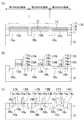
そこで、相異なる動作電圧の第1,第2,第3のMISトランジスタを有する半導体装置が提案されている(例えば特許文献1参照)。以下に、従来の半導体装置の製造方法について、図3(a) 〜(c) 及び図4(a) 〜(b) を参照しながら説明する。図3(a) 〜図4(b) は、従来の半導体装置の製造方法を工程順に示すゲート長方向の要部工程断面図である。図3(a) 〜図4(b) に示す「第1,第2,第3のMIS領域」とは、第1,第2,第3のMISトランジスタが形成される領域をいう。第2のMISトランジスタの動作電圧は、第1のMISトランジスタの動作電圧よりも低く、且つ、第3のMISトランジスタの動作電圧よりも高い。 Therefore, a semiconductor device having first, second, and third MIS transistors with different operating voltages has been proposed (see, for example, Patent Document 1). A conventional method for manufacturing a semiconductor device will be described below with reference to FIGS. 3 (a) to 3 (c) and FIGS. 4 (a) to 4 (b). FIG. 3A to FIG. 4B are cross-sectional views of main steps in the gate length direction showing the conventional method of manufacturing a semiconductor device in the order of steps. The “first, second and third MIS regions” shown in FIGS. 3A to 4B are regions where the first, second and third MIS transistors are formed. The operating voltage of the second MIS transistor is lower than the operating voltage of the first MIS transistor and higher than the operating voltage of the third MIS transistor.
まず、図3(a) に示すように、半導体基板100の上部に、素子分離領域101を選択的に形成する。これにより、半導体基板100における第1,第2,第3のMIS領域に、素子分離領域101に囲まれた第1,第2,第3の活性領域100a,100b,100cが形成される。その後、第1,第2,第3の活性領域100a,100b,100cの上部領域に、第1,第2,第3のチャネル拡散層102a,102b,102cを形成する。その後、ゲート絶縁膜形成のための1回目の熱酸化を行い、第1,第2,第3の活性領域100a,100b,100c上に、第1のシリコン酸化膜形成膜103を形成する。 First, as shown in FIG. 3A, an
次に、図3(b) に示すように、フォトリソグラフィ法により、第1のシリコン酸化膜形成膜103上に、第1,第3のMIS領域を覆い第2のMIS領域を開口するレジストパターンRe1を形成する。その後、レジストパターンRe1をマスクにして、エッチング法により、第1のシリコン酸化膜形成膜103における第2のMIS領域に形成された部分を除去する。これにより、第2の活性領域100bの表面を露出させる。その後、レジストパターンRe1を除去する。 Next, as shown in FIG. 3B, a resist pattern that covers the first and third MIS regions and opens the second MIS region on the first silicon oxide
次に、図3(c) に示すように、ゲート絶縁膜形成のための2回目の熱酸化を行い、第2の活性領域100b上に、第1のシリコン酸化膜形成膜103よりも薄い膜厚を有する第2のシリコン酸化膜形成膜104を形成する。 Next, as shown in FIG. 3C, the second thermal oxidation for forming the gate insulating film is performed, and a film thinner than the first silicon oxide
次に、図4(a) に示すように、第1,第2のシリコン酸化膜形成膜103,104上に、第1,第2のMIS領域を覆い第3のMIS領域を開口するレジストパターンRe2を形成する。その後、レジストパターンRe2をマスクにして、エッチング法により、第1のシリコン酸化膜形成膜103における第3のMIS領域に形成された部分を除去する。これにより、第3の活性領域100cの表面を露出させる。その後、レジストパターンRe2を除去する。 Next, as shown in FIG. 4A, a resist pattern that covers the first and second MIS regions and opens the third MIS region on the first and second silicon oxide
次に、図4(b) に示すように、ゲート絶縁膜形成のための3回目の熱酸化を行い、第3の活性領域100c上に、第2のシリコン酸化膜形成膜104よりも薄い膜厚を有する第3のシリコン酸化膜形成膜105を形成する。 Next, as shown in FIG. 4B, the third thermal oxidation for forming the gate insulating film is performed, and a film thinner than the second silicon oxide
その後、図示を省略するが、第1,第2,第3のシリコン酸化膜形成膜103,104,105上に、ゲート電極形成膜(図示せず)を形成する。その後、ゲート電極形成膜及び第1,第2,第3のシリコン酸化膜形成膜103,104,105を順次パターニングする。これにより、第1の活性領域100a上に、第1のシリコン酸化膜形成膜からなる第1のゲート絶縁膜(図示せず)、及びゲート電極形成膜からなる第1のゲート電極(図示せず)を順次形成する。第2の活性領域100b上に、第2のシリコン酸化膜形成膜からなる第2のゲート絶縁膜(図示せず)、及びゲート電極形成膜からなる第2のゲート電極(図示せず)を順次形成する。第3の活性領域100c上に、第3のシリコン酸化膜形成膜からなる第3のゲート絶縁膜(図示せず)、及びゲート電極形成膜からなる第3のゲート電極(図示せず)を順次形成する。このとき、既述の通り、第2のシリコン酸化膜形成膜104の膜厚は、第1のシリコン酸化膜形成膜103の膜厚よりも薄く、且つ、第3のシリコン酸化膜形成膜105の膜厚よりも厚いため、第2のゲート絶縁膜の膜厚は、第1のゲート絶縁膜の膜厚よりも薄く、且つ、第3のゲート絶縁膜の膜厚よりも厚い。 Thereafter, although not shown, a gate electrode formation film (not shown) is formed on the first, second, and third silicon oxide
以上のようにして、従来の半導体装置を製造する。 As described above, a conventional semiconductor device is manufactured.
しかしながら、従来の半導体装置では、以下に示す問題がある。 However, the conventional semiconductor device has the following problems.
従来の半導体装置の製造方法では、図3(a) に示すように、第1,第2,第3のチャネル拡散層102a,102b,102cを形成した後、1回目の熱酸化を行い、第1のシリコン酸化膜形成膜103を形成する。その後、図3(c) に示すように、2回目の熱酸化を行い、第2のシリコン酸化膜形成膜104を形成する。その後、図4(b) に示すように、3回目の熱酸化を行い、第3のシリコン酸化膜形成膜105を形成する。このように、第1,第2,第3のチャネル拡散層102a,102b,102cの形成後に、3回の熱酸化を行う。そのため、3回の熱酸化の各時に、第1,第2,第3のチャネル拡散層102a,102b,102cに含まれる導電型不純物が拡散されて、第1,第2,第3のチャネル拡散層102a,102b,102cの不純物プロファイルが変動するという問題がある。 In the conventional method of manufacturing a semiconductor device, as shown in FIG. 3A, after the first, second, and third
特に、第1,第2,第3のチャネル拡散層102a,102b,102cに含まれる導電型不純物が拡散される拡散量は、1回目の熱酸化時が最も多く、2回目の熱酸化時、3回目の熱酸化時と順に少なくなる。その理由は、次に示す通りである。一般に、厚い酸化膜を形成するためには、薄い酸化膜の形成に比べて熱酸化時間を長くする、又は、酸化温度を高くする必要がある。この場合、熱酸化時間が短い場合、又は、酸化温度が低い場合に比べて、チャネル拡散層に含まれる導電型不純物が拡散され易い。第1のシリコン酸化膜形成膜103は、第2のシリコン酸化膜形成膜104よりも膜厚が厚いため、1回目の熱酸化は、2回目の熱酸化よりも長い時間が必要とされる。また、第2のシリコン酸化膜形成膜104は、第3のシリコン酸化膜形成膜105よりも膜厚が厚いため、2回目の熱酸化は、3回目の熱酸化よりも長い時間が必要とされる。そのため、1回目の熱酸化時間が最も長く、2回目の熱酸化時間、3回目の熱酸化時間と順に短くなる。 In particular, the amount of diffusion of conductive impurities contained in the first, second, and third
また、図3(a) に示すように、第1,第2,第3の活性領域100a,100b,100cにおける酸化された部分が、第1のシリコン酸化膜形成膜として消費される。そのため、第1,第2,第3のチャネル拡散層102a,102b,102cの上部が、第1のシリコン酸化膜形成膜として消費される。その後、図3(b) に示すように、第1のシリコン酸化膜形成膜103における第2のMIS領域に形成された部分が除去される。そのため、第2のチャネル拡散層102bにおける第1のシリコン酸化膜形成膜として消費された部分が除去される。その後、図3(c) に示すように、第2の活性領域100bにおける酸化された部分が、第2のシリコン酸化膜形成膜として消費される。そのため、第2のチャネル拡散層102bの上部が、第2のシリコン酸化膜形成膜として消費される。その後、図4(a) に示すように、第1のシリコン酸化膜形成膜103における第3のMIS領域に形成された部分が除去される。そのため、第3のチャネル拡散層102cにおける第1のシリコン酸化膜形成膜として消費された部分が除去される。その後、図4(b) に示すように、第3の活性領域100cにおける酸化された部分が、第3のシリコン酸化膜形成膜として消費される。そのため、第3のチャネル拡散層102cの上部が、第3のシリコン酸化膜形成膜として消費される。そのため、第1,第2,第3のチャネル拡散層102a,102b,102cの表面高さは、形成直後の第1,第2,第3のチャネル拡散層102a,102b,102cの表面高さよりも低く(言い換えれば、第1,第2,第3のチャネル拡散層102a,102b,102cの深さは、形成直後の第1,第2,第3のチャネル拡散層102a,102b,102cの深さよりも浅く)、第1,第2,第3のチャネル拡散層102a,102b,102cの不純物プロファイルが変動するという問題がある。 Further, as shown in FIG. 3A, the oxidized portions in the first, second, and third
以上のように、3回の熱酸化の各時に、第1,第2,第3のチャネル拡散層102a,102b,102cの不純物プロファイルが変動すると共に、上部がシリコン酸化膜形成膜として消費されることに起因して、第1,第2,第3のチャネル拡散層102a,102b,102cの不純物プロファイルが変動するという問題がある。従って、所望の特性を有する第1,第2,第3のMISトランジスタを実現することができない。 As described above, the impurity profile of the first, second, and third
前記に鑑み、本発明の目的は、相異なる動作電圧の第1,第2,第3のMISトランジスタを有する半導体装置において、第1,第2,第3のチャネル拡散層の不純物プロファイルの変動を抑制することである。 In view of the above, an object of the present invention is to reduce the impurity profile of the first, second, and third channel diffusion layers in a semiconductor device having first, second, and third MIS transistors having different operating voltages. It is to suppress.
前記の目的を達成するために、本発明に係る半導体装置は、半導体基板における第1の活性領域上に第1のゲート絶縁膜を介して形成された第1のゲート電極を有する第1導電型の第1のMISトランジスタと、半導体基板における第2の活性領域上に第2のゲート絶縁膜を介して形成された第1のゲート電極よりもゲート長の短い第2のゲート電極を有する第1導電型の第2のMISトランジスタと、半導体基板における第3の活性領域上に第3のゲート絶縁膜を介して形成された第2のゲート電極よりもゲート長の短い第3のゲート電極を有する第1導電型の第3のMISトランジスタとを備え、第1のゲート絶縁膜は、第1のシリコン酸化膜と第1のシリコン酸化膜上に形成された第1の高誘電率絶縁膜とからなり、第2のゲート絶縁膜は、第2のシリコン酸化膜と第2のシリコン酸化膜上に形成された第2の高誘電率絶縁膜とからなり、第3のゲート絶縁膜は、第3のシリコン酸化膜と第3のシリコン酸化膜上に形成された第3の高誘電率絶縁膜とからなり、第2のシリコン酸化膜は、第1のシリコン酸化膜と同じ膜厚を有し、且つ、第3のシリコン酸化膜よりも厚い膜厚を有していることを特徴とし、第1の活性領域における第1のゲート絶縁膜の下の領域に形成された第2導電型の第1のチャネル拡散層と、第2の活性領域における第2のゲート絶縁膜の下の領域に形成された第2導電型の第2のチャネル拡散層と、第3の活性領域における第3のゲート絶縁膜の下の領域に形成された第2導電型の第3のチャネル拡散層とをさらに備え、第2のチャネル拡散層は、第1のチャネル拡散層よりも高い不純物濃度を有し、且つ、第3のチャネル拡散層よりも低い不純物濃度を有していることが好ましい。 In order to achieve the above object, a semiconductor device according to the present invention has a first conductivity type having a first gate electrode formed on a first active region of a semiconductor substrate via a first gate insulating film. A first MIS transistor having a second gate electrode having a shorter gate length than the first gate electrode formed on the second active region of the semiconductor substrate via the second gate insulating film. A second MIS transistor of conductivity type and a third gate electrode having a gate length shorter than that of the second gate electrode formed on the third active region of the semiconductor substrate via the third gate insulating film A first MIS transistor of the first conductivity type, wherein the first gate insulating film includes a first silicon oxide film and a first high dielectric constant insulating film formed on the first silicon oxide film. Second gate insulation Consists of a second silicon oxide film and a second high dielectric constant insulating film formed on the second silicon oxide film, and the third gate insulating film comprises a third silicon oxide film and a third silicon oxide film. A third high dielectric constant insulating film formed on the silicon oxide film, the second silicon oxide film having the same thickness as the first silicon oxide film, and the third silicon oxide film A first channel diffusion layer of the second conductivity type formed in a region under the first gate insulating film in the first active region, and a second channel A second channel diffusion layer of the second conductivity type formed in a region under the second gate insulating film in the active region, and a region under the third gate insulating film in the third active region. And a second channel diffusion layer of the second conductivity type, and the second channel diffusion layer It has a higher impurity concentration than the channel diffusion layer, and preferably has a lower impurity concentration than the third channel diffusion layer.
本発明に係る半導体装置によると、第1,第2のゲート絶縁膜の構成を、第1,第2のシリコン酸化膜と第1,第2の高誘電率絶縁膜との積層構成とする。これにより、第1のシリコン酸化膜の膜厚と第2のシリコン酸化膜の膜厚とを同じにすることができる。そのため、第1,第2,第3のチャネル拡散層の形成後に行う熱処理の回数を、第1,第2のシリコン酸化膜を形成する為の熱処理と、第3のシリコン酸化膜を形成する為の熱処理との計2回とし、従来に比べて、熱処理の回数を低減することができる。そのため、第1,第2,第3のチャネル拡散層に含まれる第2導電型不純物が拡散される回数を低減することができる。そのため、第1,第2,第3のチャネル拡散層の不純物プロファイルが変動することを抑制することができる。 According to the semiconductor device of the present invention, the first and second gate insulating films are stacked with the first and second silicon oxide films and the first and second high dielectric constant insulating films. Thereby, the film thickness of the first silicon oxide film and the film thickness of the second silicon oxide film can be made the same. For this reason, the number of heat treatments performed after the formation of the first, second, and third channel diffusion layers is set so that the heat treatment for forming the first and second silicon oxide films and the third silicon oxide film are formed. Thus, the number of heat treatments can be reduced as compared with the conventional case. Therefore, the number of times that the second conductivity type impurities contained in the first, second, and third channel diffusion layers are diffused can be reduced. Therefore, it is possible to suppress fluctuations in the impurity profiles of the first, second, and third channel diffusion layers.
加えて、第1,第2,第3のゲート絶縁膜の構成を、第1,第2,第3のシリコン酸化膜と第1,第2,第3の高誘電率絶縁膜との積層構成とし、従来に比べて、第1,第2,第3のシリコン酸化膜の膜厚を薄くすることができる。そのため、第1,第2のシリコン酸化膜を形成する為の熱処理に必要とされる時間を短くすると共に、第3のシリコン酸化膜を形成する為の熱処理に必要とされる時間を短くすることができる。そのため、2回の熱処理の各時に、第1,第2,第3のチャネル拡散層に含まれる第2導電型不純物が拡散される量を抑制し、第1,第2,第3のチャネル拡散層の不純物プロファイルが変動することを抑制することができる。 In addition, the configuration of the first, second, and third gate insulating films is a stacked configuration of the first, second, and third silicon oxide films and the first, second, and third high dielectric constant insulating films. As compared with the prior art, the thickness of the first, second and third silicon oxide films can be reduced. Therefore, the time required for the heat treatment for forming the first and second silicon oxide films is shortened, and the time required for the heat treatment for forming the third silicon oxide film is shortened. Can do. Therefore, the amount of the second conductivity type impurity contained in the first, second, and third channel diffusion layers is suppressed at each of the two heat treatments, and the first, second, and third channel diffusions are suppressed. Fluctuations in the impurity profile of the layer can be suppressed.
さらに、既述の通り、従来に比べて、第1,第2,第3のシリコン酸化膜の膜厚を薄くすることができる。そのため、第1,第2のシリコン酸化膜を形成する為の熱処理時に、第1,第2,第3のチャネル拡散層におけるシリコン酸化膜として消費される量を低減することができる。それと共に、第3のシリコン酸化膜を形成する為の熱処理時に、第3のチャネル拡散層におけるシリコン酸化膜として消費される量を低減することができる。そのため、第1,第2,第3のチャネル拡散層の表面高さが、形成直後の第1,第2,第3のチャネル拡散層の表面高さよりも低くなることを抑制し、第1,第2,第3のチャネル拡散層の不純物プロファイルが変動することを抑制することができる。 Furthermore, as described above, the first, second, and third silicon oxide films can be made thinner than the conventional one. Therefore, the amount consumed as silicon oxide films in the first, second, and third channel diffusion layers during the heat treatment for forming the first and second silicon oxide films can be reduced. At the same time, the amount consumed as the silicon oxide film in the third channel diffusion layer can be reduced during the heat treatment for forming the third silicon oxide film. Therefore, the surface height of the first, second, and third channel diffusion layers is suppressed from being lower than the surface height of the first, second, and third channel diffusion layers immediately after the formation, Fluctuations in the impurity profiles of the second and third channel diffusion layers can be suppressed.
以上のように、熱処理回数の低減、及びシリコン酸化膜の薄膜化による熱処理時間の短縮により、第1,第2,第3のチャネル拡散層の不純物プロファイルが変動することを効果的に抑制することができる。従って、所望の特性を有する第1,第2,第3のMISトランジスタを実現することができる。 As described above, it is possible to effectively suppress fluctuations in the impurity profiles of the first, second, and third channel diffusion layers by reducing the number of heat treatments and shortening the heat treatment time by thinning the silicon oxide film. Can do. Therefore, the first, second and third MIS transistors having desired characteristics can be realized.
本発明に係る半導体装置において、第2のMISトランジスタの動作電圧は、第1のMISトランジスタの動作電圧よりも低く、且つ、第3のMISトランジスタの動作電圧よりも高いことが好ましい。 In the semiconductor device according to the present invention, the operating voltage of the second MIS transistor is preferably lower than the operating voltage of the first MIS transistor and higher than the operating voltage of the third MIS transistor.
本発明に係る半導体装置において、第1の高誘電率絶縁膜、第2の高誘電率絶縁膜及び第3の高誘電率絶縁膜は、互いに同じ膜厚を有していることが好ましい。 In the semiconductor device according to the present invention, it is preferable that the first high dielectric constant insulating film, the second high dielectric constant insulating film, and the third high dielectric constant insulating film have the same film thickness.
本発明に係る半導体装置において、第1のゲート電極は、第1の金属膜と第1の金属膜上に形成された第1のシリコン膜とからなり、第2のゲート電極は、第2の金属膜と第2の金属膜上に形成された第2のシリコン膜とからなり、第3のゲート電極は、第3の金属膜と第3の金属膜上に形成された第3のシリコン膜とからなることが好ましい。 In the semiconductor device according to the present invention, the first gate electrode includes a first metal film and a first silicon film formed on the first metal film, and the second gate electrode includes the second gate electrode. The third gate electrode is formed of a metal film and a second silicon film formed on the second metal film, and the third gate electrode is formed on the third metal film and the third metal film. It is preferable to consist of.
本発明に係る半導体装置において、第1の活性領域における第1のゲート電極の側方下の領域に形成された第1導電型の第1のエクステンション領域と、第2の活性領域における第2のゲート電極の側方下の領域に形成された第1導電型の第2のエクステンション領域と、第3の活性領域における第3のゲート電極の側方下の領域に形成された第1導電型の第3のエクステンション領域とをさらに備え、第2のエクステンション領域は、第1のエクステンション領域と同じ又はそれよりも高い不純物濃度を有し、且つ、第3のエクステンション領域よりも低い不純物濃度を有していることが好ましい。 In the semiconductor device according to the present invention, a first extension region of the first conductivity type formed in a region below the first gate electrode in the first active region, and a second extension in the second active region. A second extension region of the first conductivity type formed in a region below the side of the gate electrode, and a first conductivity type formed in a region of the third active region under the side of the third gate electrode. A third extension region, and the second extension region has an impurity concentration that is the same as or higher than that of the first extension region, and has an impurity concentration lower than that of the third extension region. It is preferable.
このようにすると、第1,第2のエクステンション領域の不純物濃度が低いため、動作電圧の高い第1,第2のMISトランジスタにおいて、過剰なホットエレクトロンが発生することを抑制することができる。そのため、過剰なホットエレクトロンが第1,第2のゲート絶縁膜に入り込み、第1,第2のMISトランジスタの閾値電圧を変化させて、第1,第2のMISトランジスタの信頼性が低下することを抑制することができる。 In this case, since the impurity concentrations of the first and second extension regions are low, it is possible to suppress the occurrence of excessive hot electrons in the first and second MIS transistors having a high operating voltage. Therefore, excessive hot electrons enter the first and second gate insulating films and change the threshold voltages of the first and second MIS transistors, thereby reducing the reliability of the first and second MIS transistors. Can be suppressed.
一方、第3のエクステンション領域の不純物濃度が高いため、動作電圧の低い第3のMISトランジスタの駆動能力を向上させることができる。 On the other hand, since the impurity concentration of the third extension region is high, the driving capability of the third MIS transistor having a low operating voltage can be improved.
本発明に係る半導体装置において、第1の高誘電率絶縁膜、第2の高誘電率絶縁膜及び第3の高誘電率絶縁膜は、比誘電率が10以上の金属酸化物からなることが好ましい。 In the semiconductor device according to the present invention, the first high dielectric constant insulating film, the second high dielectric constant insulating film, and the third high dielectric constant insulating film may be made of a metal oxide having a relative dielectric constant of 10 or more. preferable.
本発明に係る半導体装置において、第1のシリコン酸化膜及び第2のシリコン酸化膜は、膜厚が3nm以上であって且つ6nm以下であり、第3のシリコン酸化膜は、膜厚が0.8nm以上であって且つ1.2nm以下であることが好ましい。 In the semiconductor device according to the present invention, the first silicon oxide film and the second silicon oxide film have a film thickness of 3 nm or more and 6 nm or less, and the third silicon oxide film has a film thickness of 0. It is preferably 8 nm or more and 1.2 nm or less.
前記の目的を達成するために、本発明に係る半導体装置の製造方法は、半導体基板における第1の活性領域上に、第1のシリコン酸化膜形成膜を形成すると共に、半導体基板における第2の活性領域上に、第1のシリコン酸化膜形成膜を形成する工程(a)と、工程(a)の後に、半導体基板における第3の活性領域上に、第1のシリコン酸化膜形成膜よりも薄い膜厚を有する第2のシリコン酸化膜形成膜を形成する工程(b)と、第1のシリコン酸化膜形成膜及び第2のシリコン酸化膜形成膜上に、高誘電率絶縁膜形成膜を形成する工程(c)と、高誘電率絶縁膜形成膜上にゲート電極形成膜を形成する工程(d)と、ゲート電極形成膜、高誘電率絶縁膜形成膜、並びに第1のシリコン酸化膜形成膜及び第2のシリコン酸化膜形成膜を順次パターニングして、第1の活性領域上に、第1のシリコン酸化膜形成膜からなる第1のシリコン酸化膜と高誘電率絶縁膜形成膜からなる第1の高誘電率絶縁膜とを有する第1のゲート絶縁膜、及びゲート電極形成膜からなる第1のゲート電極を形成し、第2の活性領域上に、第1のシリコン酸化膜形成膜からなる第2のシリコン酸化膜と高誘電率絶縁膜形成膜からなる第2の高誘電率絶縁膜とを有する第2のゲート絶縁膜、及びゲート電極形成膜からなる第2のゲート電極を形成し、且つ、第3の活性領域上に、第2のシリコン酸化膜形成膜からなる第3のシリコン酸化膜と高誘電率絶縁膜形成膜からなる第3の高誘電率絶縁膜とを有する第3のゲート絶縁膜、及びゲート電極形成膜からなる第3のゲート電極を形成する工程(e)とを備え、第2のゲート電極のゲート長は、第1のゲート電極のゲート長よりも短く、且つ、第3のゲート電極のゲート長よりも長いことを特徴とし、工程(a)の前に、第1のイオン注入により、第1の活性領域の上部領域に第2導電型の第1のチャネル拡散層を形成する工程(f)と、工程(a)の前に、第2のイオン注入により、第2の活性領域の上部領域に第2導電型の第2のチャネル拡散層を形成する工程(g)と、工程(a)の前に、第3のイオン注入により、第3の活性領域の上部領域に第2導電型の第3のチャネル拡散層を形成する工程(h)とをさらに備え、第2のイオン注入におけるドーズ量は、第1のイオン注入におけるドーズ量よりも多く、且つ、第3のイオン注入におけるドーズ量よりも少ないことが好ましい。 In order to achieve the above object, a method for manufacturing a semiconductor device according to the present invention includes forming a first silicon oxide film formation film on a first active region in a semiconductor substrate, and forming a second silicon oxide film in the semiconductor substrate. A step (a) of forming a first silicon oxide film formation film on the active region, and after the step (a), the first silicon oxide film formation film is formed on the third active region in the semiconductor substrate more than the first silicon oxide film formation film. A step (b) of forming a second silicon oxide film forming film having a thin film thickness; and a high dielectric constant insulating film forming film is formed on the first silicon oxide film forming film and the second silicon oxide film forming film. Step (c) for forming, Step (d) for forming a gate electrode forming film on the high dielectric constant insulating film forming film, Gate electrode forming film, high dielectric constant insulating film forming film, and first silicon oxide film The formation film and the second silicon oxide film formation film are sequentially formed. Turned, the first active region has a first silicon oxide film made of the first silicon oxide film forming film and a first high dielectric constant insulating film made of the high dielectric constant insulating film forming film. A first gate electrode made of a gate insulating film and a gate electrode forming film, and a second silicon oxide film made of the first silicon oxide film and a high dielectric constant on the second active region Forming a second gate insulating film having a second high dielectric constant insulating film made of an insulating film forming film and a second gate electrode made of a gate electrode forming film; and over the third active region, A third gate insulating film having a third silicon oxide film comprising a second silicon oxide film forming film and a third high dielectric constant insulating film comprising a high dielectric constant insulating film; and a gate electrode forming film. And (e) forming a third gate electrode. The gate length of the second gate electrode is shorter than the gate length of the first gate electrode and longer than the gate length of the third gate electrode, and before the step (a), The step (f) of forming the first channel diffusion layer of the second conductivity type in the upper region of the first active region by the ion implantation of the first and the second ion implantation before the step (a) A step (g) of forming a second channel diffusion layer of the second conductivity type in the upper region of the second active region, and the upper portion of the third active region by the third ion implantation before the step (a). Forming a second conductivity type third channel diffusion layer in the region, wherein a dose amount in the second ion implantation is larger than a dose amount in the first ion implantation; 3 is preferably smaller than the dose in ion implantation.
本発明に係る半導体装置の製造方法によると、第1,第2のゲート絶縁膜の構成を、第1,第2のシリコン酸化膜と第1,第2の高誘電率絶縁膜との積層構成とする。これにより、第1のシリコン酸化膜の膜厚と第2のシリコン酸化膜の膜厚とを同じにすることができる。そのため、第1,第2,第3のチャネル拡散層の形成後に行う熱処理の回数を、第1,第2のシリコン酸化膜を形成する為の熱処理(言い換えれば、第1のシリコン酸化膜形成膜を形成する為の熱処理)と、第3のシリコン酸化膜を形成する為の熱処理(言い換えれば、第2のシリコン酸化膜形成膜を形成する為の熱処理)との計2回とし、従来に比べて、熱処理の回数を低減することができる。そのため、第1,第2,第3のチャネル拡散層に含まれる第2導電型不純物が拡散される回数を低減することができる。そのため、第1,第2,第3のチャネル拡散層の不純物プロファイルが変動することを抑制することができる。 According to the method of manufacturing a semiconductor device according to the present invention, the first and second gate insulating films are formed by stacking the first and second silicon oxide films and the first and second high dielectric constant insulating films. And Thereby, the film thickness of the first silicon oxide film and the film thickness of the second silicon oxide film can be made the same. Therefore, the number of heat treatments performed after the formation of the first, second, and third channel diffusion layers is equal to the heat treatment for forming the first and second silicon oxide films (in other words, the first silicon oxide film formation film). Heat treatment for forming the third silicon oxide film) and heat treatment for forming the third silicon oxide film (in other words, heat treatment for forming the second silicon oxide film formation film), two times in total. Thus, the number of heat treatments can be reduced. Therefore, the number of times that the second conductivity type impurities contained in the first, second, and third channel diffusion layers are diffused can be reduced. Therefore, it is possible to suppress fluctuations in the impurity profiles of the first, second, and third channel diffusion layers.
加えて、第1,第2,第3のゲート絶縁膜の構成を、第1,第2,第3のシリコン酸化膜と第1,第2,第3の高誘電率絶縁膜との積層構成とし、従来に比べて、第1,第2,第3のシリコン酸化膜の膜厚を薄くすることができるため、第1,第2のシリコン酸化膜形成膜の膜厚を薄くすることができる。そのため、第1のシリコン酸化膜形成膜を形成する為の熱処理に必要とされる時間を短くすると共に、第2のシリコン酸化膜形成膜を形成する為の熱処理に必要とされる時間を短くすることができる。そのため、2回の熱処理の各時に、第1,第2,第3のチャネル拡散層に含まれる第2導電型不純物が拡散される量を抑制し、第1,第2,第3のチャネル拡散層の不純物プロファイルが変動することを抑制することができる。 In addition, the configuration of the first, second, and third gate insulating films is a stacked configuration of the first, second, and third silicon oxide films and the first, second, and third high dielectric constant insulating films. Since the thicknesses of the first, second, and third silicon oxide films can be reduced compared to the conventional case, the thicknesses of the first and second silicon oxide film forming films can be reduced. . Therefore, the time required for the heat treatment for forming the first silicon oxide film formation film is shortened, and the time required for the heat treatment for forming the second silicon oxide film formation film is shortened. be able to. Therefore, the amount of the second conductivity type impurity contained in the first, second, and third channel diffusion layers is suppressed at each of the two heat treatments, and the first, second, and third channel diffusions are suppressed. Fluctuations in the impurity profile of the layer can be suppressed.
さらに、既述の通り、従来に比べて、第1,第2,第3のシリコン酸化膜の膜厚を薄くすることができるため、第1,第2のシリコン酸化膜形成膜の膜厚を薄くすることができる。そのため、第1のシリコン酸化膜形成膜を形成する為の熱処理時に、第1,第2,第3のチャネル拡散層における第1のシリコン酸化膜形成膜として消費される量を低減することができる。それと共に、第2のシリコン酸化膜形成膜を形成する為の熱処理時に、第3のチャネル拡散層における第2のシリコン酸化膜形成膜として消費される量を低減することができる。そのため、第1,第2,第3のチャネル拡散層の表面高さが、形成直後の第1,第2,第3のチャネル拡散層の表面高さよりも低くなることを抑制し、第1,第2,第3のチャネル拡散層の不純物プロファイルが変動することを抑制することができる。 Furthermore, as described above, since the film thickness of the first, second, and third silicon oxide films can be made thinner than the conventional one, the film thickness of the first and second silicon oxide film forming films can be reduced. Can be thinned. Therefore, the amount consumed as the first silicon oxide film formation film in the first, second, and third channel diffusion layers during the heat treatment for forming the first silicon oxide film formation film can be reduced. . At the same time, the amount consumed as the second silicon oxide film forming film in the third channel diffusion layer during the heat treatment for forming the second silicon oxide film forming film can be reduced. Therefore, the surface height of the first, second, and third channel diffusion layers is suppressed from being lower than the surface height of the first, second, and third channel diffusion layers immediately after the formation, Fluctuations in the impurity profiles of the second and third channel diffusion layers can be suppressed.
以上のように、熱処理回数の低減、及びシリコン酸化膜形成膜の薄膜化による熱処理時間の短縮により、第1,第2,第3のチャネル拡散層の不純物プロファイルが変動することを効果的に抑制することができる。従って、所望の特性を有する第1,第2,第3のMISトランジスタを実現することができる。 As described above, fluctuations in the impurity profile of the first, second, and third channel diffusion layers are effectively suppressed by reducing the number of heat treatments and shortening the heat treatment time by thinning the silicon oxide film formation film. can do. Therefore, the first, second and third MIS transistors having desired characteristics can be realized.
本発明に係る半導体装置の製造方法において、工程(d)は、高誘電率絶縁膜形成膜上に、金属膜形成膜及びシリコン膜形成膜が順次積層されてなるゲート電極形成膜を形成する工程であり、工程(e)は、シリコン膜形成膜、金属膜形成膜、高誘電率絶縁膜形成膜、並びに第1のシリコン酸化膜形成膜及び第2のシリコン酸化膜形成膜を順次パターニングして、第1の活性領域上に、第1のゲート絶縁膜、及び金属膜形成膜からなる第1の金属膜とシリコン膜形成膜からなる第1のシリコン膜とを有する第1のゲート電極を形成し、第2の活性領域上に、第2のゲート絶縁膜、及び金属膜形成膜からなる第2の金属膜とシリコン膜形成膜からなる第2のシリコン膜とを有する第2のゲート電極を形成し、且つ、第3の活性領域上に、第3のゲート絶縁膜、及び金属膜形成膜からなる第3の金属膜とシリコン膜形成膜からなる第3のシリコン膜とを有する第3のゲート電極を形成する工程であることが好ましい。 In the method for manufacturing a semiconductor device according to the present invention, the step (d) is a step of forming a gate electrode forming film in which a metal film forming film and a silicon film forming film are sequentially laminated on the high dielectric constant insulating film forming film. In step (e), the silicon film forming film, the metal film forming film, the high dielectric constant insulating film forming film, the first silicon oxide film forming film, and the second silicon oxide film forming film are sequentially patterned. Forming a first gate electrode having a first gate insulating film and a first metal film made of a metal film forming film and a first silicon film made of a silicon film forming film on the first active region; And a second gate electrode having a second gate insulating film, a second metal film made of a metal film forming film, and a second silicon film made of a silicon film forming film on the second active region. And forming a third active region on the third active region Over gate insulating film, and is preferably a step of forming a third gate electrode and a third silicon film made of the third metal film and the silicon film forming film made of a metal film formation film.
本発明に係る半導体装置の製造方法において、工程(e)の後に、第4のイオン注入により、第1の活性領域における第1のゲート電極の側方下の領域に第1導電型の第1のエクステンション領域を形成する工程(i)と、工程(e)の後に、第5のイオン注入により、第2の活性領域における第2のゲート電極の側方下の領域に第1導電型の第2のエクステンション領域を形成する工程(j)と、工程(e)の後に、第6のイオン注入により、第3の活性領域における第3のゲート電極の側方下の領域に第1導電型の第3のエクステンション領域を形成する工程(k)とをさらに備え、第5のイオン注入におけるドーズ量は、第4のイオン注入におけるドーズ量と同じ又はそれよりも多く、且つ、第6のイオン注入におけるドーズ量よりも少ないことが好ましい。 In the method of manufacturing a semiconductor device according to the present invention, after the step (e), the first conductivity type first is formed in the region under the side of the first gate electrode in the first active region by the fourth ion implantation. After the step (i) and the step (e) of forming the extension region, the first conductivity type first region is formed in a region below the second gate electrode in the second active region by the fifth ion implantation. After the step (j) of forming the second extension region and the step (e), the first conductivity type is formed in the region under the third gate electrode in the third active region by the sixth ion implantation. And a step (k) of forming a third extension region, wherein a dose amount in the fifth ion implantation is the same as or larger than a dose amount in the fourth ion implantation, and a sixth ion implantation is performed. Than the dose in It is preferable not.
このようにすると、第2のエクステンション領域の不純物濃度を、第1のエクステンション領域の不純物濃度と同じ又はそれよりも高くし、且つ、第3のエクステンション領域の不純物濃度よりも低くすることができる。 In this way, the impurity concentration of the second extension region can be the same as or higher than the impurity concentration of the first extension region, and lower than the impurity concentration of the third extension region.
これにより、動作電圧の高い第1,第2のMISトランジスタにおいて、過剰なホットエレクトロンが発生することを抑制することができる。そのため、過剰なホットエレクトロンが第1,第2のゲート絶縁膜に入り込み、第1,第2のMISトランジスタの閾値電圧を変化させて、第1,第2のMISトランジスタの信頼性が低下することを抑制することができる。 Thereby, it is possible to suppress the occurrence of excessive hot electrons in the first and second MIS transistors having a high operating voltage. Therefore, excessive hot electrons enter the first and second gate insulating films and change the threshold voltages of the first and second MIS transistors, thereby reducing the reliability of the first and second MIS transistors. Can be suppressed.
一方、動作電圧の低い第3のMISトランジスタの駆動能力を向上させることができる。 On the other hand, the driving capability of the third MIS transistor having a low operating voltage can be improved.
本発明に係る半導体装置及びその製造方法によると、熱処理回数の低減、及びシリコン酸化膜の薄膜化による熱処理時間の短縮により、第1,第2,第3のチャネル拡散層の不純物プロファイルが変動することを効果的に抑制することができる。従って、所望の特性を有する第1,第2,第3のMISトランジスタを実現することができる。 According to the semiconductor device and the manufacturing method thereof according to the present invention, the impurity profile of the first, second, and third channel diffusion layers varies due to the reduction in the number of heat treatments and the shortening of the heat treatment time by thinning the silicon oxide film. This can be effectively suppressed. Therefore, the first, second and third MIS transistors having desired characteristics can be realized.
以下に、本発明の実施形態について図面を参照しながら説明する。 Embodiments of the present invention will be described below with reference to the drawings.
(一実施形態)
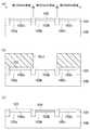
以下に、本発明の一実施形態に係る半導体装置の製造方法について、図1(a) 〜(c) 及び図2(a) 〜(c) を参照しながら説明する。図1(a) 〜図2(c) は、本発明の一実施形態に係る半導体装置の製造方法を工程順に示すゲート長方向の要部工程断面図である。図1(a) 〜図2(c) において、左側に示す「第1のMIS領域」とは、第1のMISトランジスタが形成される領域を示し、中央に示す「第2のMIS領域」とは、第2のMISトランジスタが形成される領域を示し、右側に示す「第3のMIS領域」とは、第3のMISトランジスタが形成される領域を示す。第2のMISトランジスタの動作電圧Vdd2は、第1のMISトランジスタの動作電圧Vdd1よりも低く、且つ、第3のMISトランジスタの動作電圧Vdd3よりも高い(Vdd1>Vdd2>Vdd3)。第1,第2のMISトランジスタとしては、例えばIO(Input Output)用MISトランジスタが挙げられる。第3のMISトランジスタとしては、例えば内部回路用MISトランジスタが挙げられる。(One embodiment)
A method for manufacturing a semiconductor device according to an embodiment of the present invention will be described below with reference to FIGS. 1 (a) to (c) and FIGS. 2 (a) to (c). FIG. 1A to FIG. 2C are principal part process cross-sectional views in the gate length direction showing a semiconductor device manufacturing method according to an embodiment of the present invention in the order of processes. In FIG. 1 (a) to FIG. 2 (c), the “first MIS region” shown on the left side indicates the region where the first MIS transistor is formed, and the “second MIS region” shown in the center. Indicates a region in which the second MIS transistor is formed, and a “third MIS region” on the right side indicates a region in which the third MIS transistor is formed. The operating voltage Vdd2 of the second MIS transistor is lower than the operating voltage Vdd1 of the first MIS transistor and higher than the operating voltage Vdd3 of the third MIS transistor (Vdd1>Vdd2> Vdd3). Examples of the first and second MIS transistors include IO (Input Output) MIS transistors. An example of the third MIS transistor is an internal circuit MIS transistor.
まず、図1(a) に示すように、例えば埋め込み素子分離(Shallow Trench Isolation:STI)法により、例えばシリコンからなる半導体基板10の上部に、トレンチ内に絶縁膜が埋め込まれた素子分離領域11を選択的に形成する。これにより、半導体基板10における第1,第2,第3のMIS領域に、素子分離領域11に囲まれた第1,第2,第3の活性領域10a,10b,10cが形成される。その後、イオン注入法により、半導体基板10における第1,第2,第3のMIS領域に、例えばボロン(B)等のp型不純物を注入した後、半導体基板10に対して熱処理を行う。これにより、半導体基板10における第1,第2,第3のMIS領域に、p型の第1,第2,第3のウェル領域(図示せず)を形成する。 First, as shown in FIG. 1A, an
その後、第1のVt注入(第1のイオン注入)により、例えばエネルギーが10keV〜15keV,ドーズ量が3×1012/cm2〜1×1013/cm2の条件で、第1の活性領域10aに、例えばボロン(B)等のp型不純物を注入する。これにより、第1の活性領域10aの上部領域に、p型の第1のチャネル拡散層12aを形成する。その後、第2のVt注入(第2のイオン注入)により、例えばエネルギーが10keV〜15keV,ドーズ量が5×1012/cm2〜2×1013/cm2の条件で、第2の活性領域10bに、例えばB等のp型不純物を注入する。これにより、第2の活性領域10bの上部領域に、p型の第2のチャネル拡散層12bを形成する。その後、第3のVt注入(第3のイオン注入)により、例えばエネルギーが5keV〜10keV,ドーズ量が6×1012/cm2〜3×1013/cm2の条件で、第3の活性領域10cに、例えばB等のp型不純物を注入する。これにより、第3の活性領域10cの上部領域に、p型の第3のチャネル拡散層12cを形成する。ここで、「第1,第2,第3のVt注入」とは、第1,第2,第3のチャネル拡散層を形成する為のイオン注入をいう。第1,第2,第3のVt注入を行う順序は、上記の順序に限定されるものではなく、順不同である。After that, by the first Vt implantation (first ion implantation), for example, the first active region under the conditions of energy of 10 keV to 15 keV and dose of 3 × 10¹² / cm2 to 1 × 10¹³ / cm2. A p-type impurity such as boron (B) is implanted into 10a. Thereby, the p-type first
第1,第2,第3のVt注入におけるドーズ量の多少関係は、次に示す通りである。第2のVt注入におけるドーズ量Dvt2は、第1のVt注入におけるドーズ量Dvt1よりも多く、且つ、第3のVt注入におけるドーズ量Dvt3よりも少ない(Dvt1<Dvt2<Dvt3)。 The relationship between the dose amounts in the first, second, and third Vt implantations is as follows. The dose amount Dvt2 in the second Vt implantation is larger than the dose amount Dvt1 in the first Vt implantation and smaller than the dose amount Dvt3 in the third Vt implantation (Dvt1 <Dvt2 <Dvt3).
このように、ドーズ量がDvt1<Dvt2<Dvt3の関係を満たすため、第2のチャネル拡散層12bは、第1のチャネル拡散層12aよりも高い不純物濃度を有し、且つ、第3のチャネル拡散層12cよりも低い不純物濃度を有する。 Thus, since the dose amount satisfies the relationship of Dvt1 <Dvt2 <Dvt3, the second
その後、例えばウェット酸化法により、例えば900℃の下、第1,第2,第3の活性領域10a,10b,10c上に、例えば膜厚が3.3nmのシリコン酸化膜からなる第1のシリコン酸化膜形成膜13を形成する。第1のシリコン酸化膜形成膜13の膜厚は、例えば3nm以上であって且つ6nm以下であることが好ましい。 Thereafter, the first silicon made of, for example, a 3.3 nm-thickness silicon oxide film is formed on the first, second, and third
次に、図1(b) に示すように、リソグラフィ法により、第1のシリコン酸化膜形成膜13上に、第1,第2のMIS領域を覆い第3のMIS領域を開口するレジストパターンReを形成する。その後、レジストパターンReをマスクにして、第1のシリコン酸化膜形成膜13における第3のMIS領域に形成された部分を除去し、第3の活性領域10cの表面を露出させる。その後、レジストパターンReを除去する。 Next, as shown in FIG. 1B, a resist pattern Re that covers the first and second MIS regions and opens the third MIS region on the first silicon oxide
このようにして、第1,第2の活性領域10a,10b上に、第1のシリコン酸化膜形成膜13を形成する。 In this way, the first silicon oxide
次に、図1(c) に示すように、例えばISSG(In-Situ Steam Generation)酸化法により、例えば900℃の下、第3の活性領域10c上に、例えば膜厚が1.0nmのシリコン酸化膜からなる第2のシリコン酸化膜形成膜14を形成する。第2のシリコン酸化膜形成膜14の膜厚は、例えば0.8nm以上であって且つ1.2nm以下であることが好ましい。 Next, as shown in FIG. 1C, silicon having a film thickness of, for example, 1.0 nm is formed on the third
次に、図2(a) に示すように、例えば有機金属化学気相堆積(Metal Organic Chemical Vapor Deposition:MOCVD)法、又はALD(Atomic Layer Deposition)法等により、第1のシリコン酸化膜形成膜13及び第2のシリコン酸化膜形成膜14上に、例えば膜厚が2.5nmのHfO2又はHfSiON等からなる高誘電率絶縁膜形成膜15を形成する。高誘電率絶縁膜形成膜15は、比誘電率が例えば10以上の金属酸化物からなることが好ましい。Next, as shown in FIG. 2A, the first silicon oxide film formation film is formed by, for example, a metal organic chemical vapor deposition (MOCVD) method or an ALD (Atomic Layer Deposition) method. A high dielectric constant insulating
その後、例えばCVD(Chemical Vapor Deposition)法、ALD法又はスパッタ法等により、高誘電率絶縁膜形成膜15上に、例えば膜厚が10nm〜15nmの窒化チタン(TiN)からなる金属膜形成膜16を形成する。 Thereafter, a metal
その後、例えばCVD法により、金属膜形成膜16上に、例えば膜厚が30nm〜100nmのポリシリコン膜からなるシリコン膜形成膜17を形成する。 Thereafter, a silicon film forming film 17 made of a polysilicon film having a film thickness of, for example, 30 nm to 100 nm is formed on the metal
このようにして、高誘電率絶縁膜形成膜15上に、金属膜形成膜16とシリコン膜形成膜17とからなるゲート電極形成膜17Xを形成する。 In this manner, the gate
次に、図2(b) に示すように、フォトリソグラフィ法により、シリコン膜形成膜17上に、第1,第2,第3のゲートパターン形状を有するレジストパターン(図示せず)を形成する。このとき、第2のゲートパターン形状のゲート長方向の幅W2が、第1のゲートパターン形状のゲート長方向の幅W1よりも短く、且つ、第3のゲートパターン形状のゲート長方向の幅W3よりも長くなる(W1>W2>W3)ように、レジストパターンを形成する。 Next, as shown in FIG. 2B, resist patterns (not shown) having first, second, and third gate pattern shapes are formed on the silicon film forming film 17 by photolithography. . At this time, the width W2 in the gate length direction of the second gate pattern shape is shorter than the width W1 in the gate length direction of the first gate pattern shape, and the width W3 in the gate length direction of the third gate pattern shape. The resist pattern is formed so as to be longer (W1> W2> W3).
その後、レジストパターンをマスクにして、エッチング法により、シリコン膜形成膜17、金属膜形成膜16、高誘電率絶縁膜形成膜15、並びに第1のシリコン酸化膜形成膜13及び第2のシリコン酸化膜形成膜14を順次パターニングする。これにより、第1の活性領域10a上に、第1のシリコン酸化膜13a、第1の高誘電率絶縁膜15a、第1の金属膜16a、及び第1のシリコン膜17aを順次形成する。第2の活性領域10b上に、第2のシリコン酸化膜13b、第2の高誘電率絶縁膜15b、第2の金属膜16b、及び第2のシリコン膜17bを順次形成する。第3の活性領域10c上に、第3のシリコン酸化膜14c、第3の高誘電率絶縁膜15c、第3の金属膜16c、及び第3のシリコン膜17cを順次形成する。その後、レジストパターンを除去する。 Thereafter, using the resist pattern as a mask, the silicon film forming film 17, the metal
このようにして、第1の活性領域10a上に、第1のシリコン酸化膜13aと第1の高誘電率絶縁膜15aとからなる第1のゲート絶縁膜13A、及び第1の金属膜16aと第1のシリコン膜17aとからなる第1のゲート電極17Aを形成する。第2の活性領域10b上に、第2のシリコン酸化膜13bと第2の高誘電率絶縁膜15bとからなる第2のゲート絶縁膜13B、及び第2の金属膜16bと第2のシリコン膜17bとからなる第2のゲート電極17Bを形成する。第3の活性領域10c上に、第3のシリコン酸化膜14cと第3の高誘電率絶縁膜15cとからなる第3のゲート絶縁膜14C、及び第3の金属膜16cと第3のシリコン膜17cとからなる第3のゲート電極17Cを形成する。 In this way, the first
ここで、既述の通り、第1,第2,第3のゲートパターン形状のゲート長方向の幅がW1>W2>W3の関係を満たすため、第2のゲート電極17Bのゲート長Lg2は、第1のゲート電極17Aのゲート長Lg1よりも短く、且つ、第3のゲート電極17Cのゲート長Lg3よりも長い(Lg1>Lg2>Lg3)。具体的には例えば、ゲート長Lg1=250nm,ゲート長Lg2=150nm,ゲート長Lg3=30nmである。 Here, as described above, since the width in the gate length direction of the first, second, and third gate pattern shapes satisfies the relationship of W1> W2> W3, the gate length Lg2 of the
その後、第1のゲート電極17Aをマスクにして、第1のEx注入(第4のイオン注入)により、例えばエネルギーが20keV〜45keV,ドーズ量が3×1013/cm2〜3×1014/cm2の条件で、第1の活性領域10aに、例えばヒ素(As)等のn型不純物を注入する。これにより、第1の活性領域10aにおける第1のゲート電極17Aの側方下の領域にn型の第1のエクステンション領域18aを自己整合的に形成する。その後、第2のゲート電極17Bをマスクにして、第2のEx注入(第5のイオン注入)により、例えばエネルギーが10keV〜30keV,ドーズ量が3×1013/cm2〜3×1014/cm2の条件で、第2の活性領域10bに、例えばAs等のn型不純物を注入する。これにより、第2の活性領域10bにおける第2のゲート電極17Bの側方下の領域にn型の第2のエクステンション領域18bを自己整合的に形成する。その後、第3のゲート電極17Cをマスクにして、第3のEx注入(第6のイオン注入)により、例えばエネルギーが1keV〜3keV,ドーズ量が5×1014/cm2〜3×1015/cm2の条件で、第3の活性領域10cに、例えばAs等のn型不純物を注入する。これにより、第3の活性領域10cにおける第3のゲート電極17Cの側方下の領域にn型の第3のエクステンション領域18cを自己整合的に形成する。ここで、「第1,第2,第3のEx注入」とは、第1,第2,第3のエクステンション領域を形成する為のイオン注入をいう。第1,第2,第3のEx注入を行う順序は、上記の順序に限定されるものではなく、順不同である。After that, with the
第1,第2,第3のEx注入におけるエネルギーの大小関係は、次に示す通りである。第2のEx注入におけるエネルギーEex2は、第1のEx注入におけるエネルギーEex1よりも小さく、且つ、第3のEx注入におけるエネルギーEex3よりも大きい(Eex1>Eex2>Eex3)。 The magnitude relationship of energy in the first, second, and third Ex implantations is as follows. The energy Eex2 in the second Ex implantation is smaller than the energy Eex1 in the first Ex implantation and larger than the energy Eex3 in the third Ex implantation (Eex1> Eex2> Eex3).
このように、エネルギーがEex1>Eex2>Eex3の関係を満たすため、第2のエクステンション領域18bの深さは、第1のエクステンション領域18aの深さよりも浅く、且つ、第3のエクステンション領域18cの深さよりも深い。 Thus, since the energy satisfies the relationship Eex1> Eex2> Eex3, the depth of the
第1,第2,第3のEx注入におけるドーズ量の多少関係は、次に示す通りである。第2のEx注入におけるドーズ量Dex2は、第1のEx注入におけるドーズ量Dex1と同じ又はそれよりも多く、且つ、第3のEx注入におけるドーズ量Dex3よりも少ない(Dex1≦Dex2<Dex3)。 The relationship between the dose amounts in the first, second, and third Ex implantations is as follows. The dose amount Dex2 in the second Ex implantation is the same as or larger than the dose amount Dex1 in the first Ex implantation, and is smaller than the dose amount Dex3 in the third Ex implantation (Dex1 ≦ Dex2 <Dex3).
このように、ドーズ量がDex1≦Dex2<Dex3の関係を満たすため、第2のエクステンション領域18bは、第1のエクステンション領域18aと同じ又はそれよりも高い不純物濃度を有し、且つ、第3のエクステンション領域18cよりも低い不純物濃度を有する。 Thus, since the dose amount satisfies the relationship of Dex1 ≦ Dex2 <Dex3, the
次に、図2(c) に示すように、例えばCVD法により、半導体基板10上の全面に、例えば膜厚が30nm〜40nmのシリコン酸化膜からなるサイドウォール用絶縁膜を形成する。その後、サイドウォール用絶縁膜に対して異方性エッチングを行う。これにより、第1,第2,第3のゲート電極17A,17B,17Cの側面上に、第1,第2,第3のサイドウォール19a,19b,19cを形成する。 Next, as shown in FIG. 2C, a sidewall insulating film made of a silicon oxide film having a film thickness of, for example, 30 nm to 40 nm is formed on the entire surface of the
その後、第1,第2,第3のゲート電極17A,17B,17C、及び第1,第2,第3のサイドウォール19a,19b,19cをマスクにして、S/D注入により、例えばエネルギーが10keV〜20keV,ドーズ量が1×1015/cm2〜7×1015/cm2の条件で、第1,第2,第3の活性領域10a,10b,10cに、例えばAs等のn型不純物を注入する。これにより、第1,第2,第3の活性領域10a,10b,10cにおける第1,第2,第3のサイドウォール19a,19b,19cの外側方下の領域にn型の第1,第2,第3のソースドレイン領域20a,20b,20cを自己整合的に形成する。ここで、「S/D注入」とは、第1,第2,第3のソースドレイン領域を形成する為のイオン注入をいう。その後、熱処理により、第1,第2,第3のソースドレイン領域20a,20b,20cに含まれるn型不純物を活性化させる。Then, for example, energy is obtained by S / D implantation using the first, second, and
以上のようにして、本実施形態に係る半導体装置、即ち、動作電圧が例えば2.5Vのn型の第1のMISトランジスタTr1、動作電圧が例えば1.8Vのn型の第2のMISトランジスタTr2、及び動作電圧が例えば1.0Vのn型の第3のMISトランジスタTr3を備えた半導体装置を製造することができる。 As described above, the semiconductor device according to the present embodiment, that is, the n-type first MIS transistor Tr1 having an operating voltage of, for example, 2.5V, and the n-type second MIS transistor having an operating voltage of, for example, 1.8V A semiconductor device provided with an n-type third MIS transistor Tr3 having Tr2 and an operating voltage of, for example, 1.0 V can be manufactured.
以下に、本発明の一実施形態に係る半導体装置の構成について、図2(c) を参照しながら説明する。 The configuration of the semiconductor device according to one embodiment of the present invention will be described below with reference to FIG.
図2(c) に示すように、半導体基板10における第1のMIS領域に、n型の第1のMISトランジスタTr1が設けられている。半導体基板10における第2のMIS領域に、n型の第2のMISトランジスタTr2が設けられている。半導体基板10における第3のMIS領域に、n型の第3のMISトランジスタTr3が設けられている。 As shown in FIG. 2C, an n-type first MIS transistor Tr1 is provided in the first MIS region of the
第2のMISトランジスタTr2の動作電圧Vdd2は、第1のMISトランジスタTr1の動作電圧Vdd1よりも低く、且つ、第3のMISトランジスタTr3の動作電圧Vdd3よりも高い(Vdd1>Vdd2>Vdd3)。 The operating voltage Vdd2 of the second MIS transistor Tr2 is lower than the operating voltage Vdd1 of the first MIS transistor Tr1 and higher than the operating voltage Vdd3 of the third MIS transistor Tr3 (Vdd1> Vdd2> Vdd3).
第1のMISトランジスタTr1は、図2(c) に示すように、第1の活性領域10a上に形成された第1のシリコン酸化膜13a及び第1の高誘電率絶縁膜15aからなる第1のゲート絶縁膜13Aと、第1のゲート絶縁膜13A上に形成された第1の金属膜16a及び第1のシリコン膜17aからなる第1のゲート電極17Aと、第1の活性領域10aにおける第1のゲート絶縁膜13Aの下の領域に形成されたp型の第1のチャネル拡散層12aと、第1の活性領域10aにおける第1のゲート電極17Aの側方下の領域に形成されたn型の第1のエクステンション領域18aと、第1のゲート電極17Aの側面上に形成された第1のサイドウォール19aと、第1の活性領域10aにおける第1のサイドウォール19aの外側方下の領域に形成されたn型の第1のソースドレイン領域20aとを備えている。 As shown in FIG. 2C, the first MIS transistor Tr1 includes a first
第2のMISトランジスタTr2は、図2(c) に示すように、第2の活性領域10b上に形成された第2のシリコン酸化膜13b及び第2の高誘電率絶縁膜15bからなる第2のゲート絶縁膜13Bと、第2のゲート絶縁膜13B上に形成された第2の金属膜16b及び第2のシリコン膜17bからなる第2のゲート電極17Bと、第2の活性領域10bにおける第2のゲート絶縁膜13Bの下の領域に形成されたp型の第2のチャネル拡散層12bと、第2の活性領域10bにおける第2のゲート電極17Bの側方下の領域に形成されたn型の第2のエクステンション領域18bと、第2のゲート電極17Bの側面上に形成された第2のサイドウォール19bと、第2の活性領域10bにおける第2のサイドウォール19bの外側方下の領域に形成されたn型の第2のソースドレイン領域20bとを備えている。 As shown in FIG. 2C, the second MIS transistor Tr2 includes a second
第3のMISトランジスタTr3は、図2(c) に示すように、第3の活性領域10c上に形成された第3のシリコン酸化膜14c及び第3の高誘電率絶縁膜15cからなる第3のゲート絶縁膜14Cと、第3のゲート絶縁膜14C上に形成された第3の金属膜16c及び第3のシリコン膜17cからなる第3のゲート電極17Cと、第3の活性領域10cにおける第3のゲート絶縁膜14Cの下の領域に形成されたp型の第3のチャネル拡散層12cと、第3の活性領域10cにおける第3のゲート電極17Cの側方下の領域に形成されたn型の第3のエクステンション領域18cと、第3のゲート電極17Cの側面上に形成された第3のサイドウォール19cと、第3の活性領域10cにおける第3のサイドウォール19cの外側方下の領域に形成されたn型の第3のソースドレイン領域20cとを備えている。 As shown in FIG. 2C, the third MIS transistor Tr3 includes a third
第2のシリコン酸化膜13bは、第1のシリコン酸化膜13aと同じ膜厚を有し、且つ、第3のシリコン酸化膜14cよりも厚い膜厚を有している。第1,第2のシリコン酸化膜13a,13bの膜厚は、例えば3nm以上であって且つ6nm以下であることが好ましい。第3のシリコン酸化膜14cの膜厚は、例えば0.8nm以上であって且つ1.2nm以下であることが好ましい。 The second
第1,第2,第3の高誘電率絶縁膜15a,15b,15cは、互いに同じ材料からなり、且つ、互いに同じ膜厚を有している。 The first, second and third high dielectric constant insulating
具体的には例えば、第1,第2のシリコン酸化膜13a,13bの膜厚が3.3nmであり、第1,第2の高誘電率絶縁膜15a,15bの膜厚が2.5nmである場合、第1,第2のゲート絶縁膜13A,13Bの物理的膜厚は、5.8nm(=3.3nm+2.5nm)であり、第1,第2のゲート絶縁膜13A,13Bの電気的膜厚は、3.5nmである。第3のシリコン酸化膜14cの膜厚が1.0nmであり、第3の高誘電率絶縁膜15cの膜厚が2.5nmである場合、第3のゲート絶縁膜14Cの物理的膜厚は、3.5nm(=1.0nm+2.5nm)であり、第3のゲート絶縁膜14Cの電気的膜厚は、1.3nmである。 Specifically, for example, the film thickness of the first and second
第2のゲート電極17Bのゲート長Lg2は、第1のゲート電極17Aのゲート長Lg1よりも短く、且つ、第3のゲート電極17Cのゲート長Lg3よりも長い(Lg1>Lg2>Lg3)。 The gate length Lg2 of the
第1,第2,第3の金属膜16a,16b,16cは、互いに同じ材料からなり、且つ、互いに同じ膜厚を有している。 The first, second and
第1,第2,第3のシリコン膜17a,17b,17cは、互いに同じ材料からなり、且つ、互いに同じ膜厚を有している。 The first, second and
第2のチャネル拡散層12bは、第1のチャネル拡散層12aよりも高い不純物濃度を有し、且つ、第3のチャネル拡散層12cよりも低い不純物濃度を有している。 The second
第2のエクステンション領域18bは、第1のエクステンション領域18aよりも浅い深さを有し、且つ、第3のエクステンション領域18cよりも深い深さを有している。第2のエクステンション領域18bは、第1のエクステンション領域18aと同じ又はそれよりも高い不純物濃度を有し、且つ、第3のエクステンション領域18cよりも低い不純物濃度を有している。 The
以下に示す構成を採用することにより、相異なる動作電圧Vdd1,Vdd2,Vdd3の第1,第2,第3のMISトランジスタTr1,Tr2,Tr3を実現する。 By adopting the following configuration, the first, second, and third MIS transistors Tr1, Tr2, and Tr3 having different operating voltages Vdd1, Vdd2, and Vdd3 are realized.
−第1のMISトランジスタTr1−
第1のMISトランジスタTr1と第2のMISトランジスタTr2との構成上の相違点は、次に示す点である。第1のゲート電極17Aのゲート長Lg1は、第2のゲート電極17Bのゲート長Lg2よりも長い(Lg1>Lg2)。-First MIS transistor Tr1-
The difference in configuration between the first MIS transistor Tr1 and the second MIS transistor Tr2 is as follows. The gate length Lg1 of the
第1のMISトランジスタTr1に印加される動作電圧Vdd1は、第2のMISトランジスタTr2に印加される動作電圧Vdd2よりも高い(Vdd1>Vdd2)ため、第1のゲート電極13Aのゲート長Lg1を、第2のゲート電極13Bのゲート長Lg2よりも長くする(Lg1>Lg2)必要がある。その理由は、次に示す通りである。第1のゲート電極のゲート長が短いと、ホットキャリア(大きなエネルギーを持つキャリア)が発生し、ホットキャリアが第1のゲート絶縁膜に入り込み、第1のMISトランジスタの閾値電圧を変化させるため、第1のMISトランジスタの信頼性が低下するという不具合が生じる。 Since the operating voltage Vdd1 applied to the first MIS transistor Tr1 is higher than the operating voltage Vdd2 applied to the second MIS transistor Tr2 (Vdd1> Vdd2), the gate length Lg1 of the
そこで、ゲート長Lg1を、ゲート長Lg2よりも長くする(Lg1>Lg2)。これにより、第1のMISトランジスタTr1の信頼性の低下を招くことなく、第1のMISトランジスタTr1に、動作電圧Vdd2よりも高い動作電圧Vdd1(Vdd1>Vdd2)を印加することができる。 Therefore, the gate length Lg1 is made longer than the gate length Lg2 (Lg1> Lg2). As a result, the operating voltage Vdd1 (Vdd1> Vdd2) higher than the operating voltage Vdd2 can be applied to the first MIS transistor Tr1 without degrading the reliability of the first MIS transistor Tr1.
加えて、動作電圧Vdd1は最も高いため、第1のゲート絶縁膜13Aの破壊を招くことのないように、第1のゲート絶縁膜13Aの物理的膜厚を厚くする必要がある。 In addition, since the operating voltage Vdd1 is the highest, it is necessary to increase the physical thickness of the first
そこで、第1のゲート絶縁膜13Aの構成を、第1のシリコン酸化膜13aと第1の高誘電率絶縁膜15aとの積層構成とする。これにより、第1のゲート絶縁膜13Aの物理的膜厚を厚くすることができる。そのため、第1のゲート絶縁膜13Aの耐圧を高くすることができるので、第1のMISトランジスタTr1に動作電圧Vdd1が印加されることがあっても、第1のゲート絶縁膜13aが破壊されることを抑制することができる。 Therefore, the configuration of the first
−第2のMISトランジスタTr2−
動作電圧Vdd2は高いものの動作電圧Vdd1よりも低いため、第2のMISトランジスタTr2の駆動能力の低下を招くことのないように、第2のゲート絶縁膜13Bの電気的膜厚を薄くする必要がある。-Second MIS transistor Tr2-
Although the operating voltage Vdd2 is high but lower than the operating voltage Vdd1, it is necessary to reduce the electrical film thickness of the second
そこで、第2のゲート絶縁膜13Bの構成を、第2のシリコン酸化膜13bと第2の高誘電率絶縁膜15bとの積層構成とする。これにより、第2のゲート絶縁膜13Bの電気的膜厚を薄くすることができる。そのため、第2のMISトランジスタTr2の駆動能力が低下することを抑制することができる。 Therefore, the configuration of the second
なお、従来の半導体装置において、
・第1のシリコン酸化膜からなる第1のゲート絶縁膜の膜厚を、第2のシリコン酸化膜からなる第2のゲート絶縁膜の膜厚と同じにし、且つ、
・第1のゲート電極のゲート長を、第2のゲート電極のゲート長よりも長くした場合、以下に示す不具合が生じる。In the conventional semiconductor device,
The film thickness of the first gate insulating film made of the first silicon oxide film is made the same as the film thickness of the second gate insulating film made of the second silicon oxide film, and
When the gate length of the first gate electrode is longer than the gate length of the second gate electrode, the following problems occur.
第1に例えば、第1,第2のゲート絶縁膜の膜厚を、第1のMISトランジスタに適した膜厚にした場合(即ち、第2のゲート絶縁膜の膜厚が、第2のMISトランジスタに適した膜厚ではなく、第2のゲート絶縁膜の膜厚が厚い場合)、以下に示す不具合が生じる。 First, for example, when the thickness of the first and second gate insulating films is set to a thickness suitable for the first MIS transistor (that is, the thickness of the second gate insulating film is the second MIS). If the thickness of the second gate insulating film is not suitable for the transistor but the second gate insulating film is thick), the following problems occur.
第2のゲート絶縁膜が厚い(即ち、第2のシリコン酸化膜が厚い)と、第2のMISトランジスタの駆動能力が低下するという不具合が生じる。 If the second gate insulating film is thick (that is, the second silicon oxide film is thick), the driving capability of the second MIS transistor is degraded.
そのため、第1,第2のゲート絶縁膜の構成が第1,第2のシリコン酸化膜の単層構成の場合、第2のゲート絶縁膜の膜厚を、第1のゲート絶縁膜の膜厚よりも薄くせざるを得ず、第2のゲート絶縁膜の膜厚を、第1のゲート絶縁膜の膜厚と同じにすることができない。 Therefore, when the configuration of the first and second gate insulating films is a single layer configuration of the first and second silicon oxide films, the thickness of the second gate insulating film is set to the thickness of the first gate insulating film. Therefore, the thickness of the second gate insulating film cannot be made equal to the thickness of the first gate insulating film.
第2に例えば、第1,第2のゲート絶縁膜の膜厚を、第2のMISトランジスタに適した膜厚にした場合(即ち、第1のゲート絶縁膜の膜厚が、第1のMISトランジスタに適した膜厚ではなく、第1のゲート絶縁膜の膜厚が薄い場合)、以下に示す不具合が生じる。 Second, for example, when the thickness of the first and second gate insulating films is set to a thickness suitable for the second MIS transistor (that is, the thickness of the first gate insulating film is the first MIS). If the thickness of the first gate insulating film is small (not the thickness suitable for the transistor), the following problems occur.
第1のゲート絶縁膜が薄い(即ち、第1のシリコン酸化膜が薄い)と、第1のゲート絶縁膜の耐圧が低下し、第1のゲート絶縁膜が破壊されるという不具合が生じる。 If the first gate insulating film is thin (that is, the first silicon oxide film is thin), the breakdown voltage of the first gate insulating film is lowered, and the first gate insulating film is destroyed.
そのため、第1,第2のゲート絶縁膜の構成が第1,第2のシリコン酸化膜の単層構成の場合、第1のゲート絶縁膜の膜厚を、第2のゲート絶縁膜の膜厚よりも厚くせざるを得ず、第1のゲート絶縁膜の膜厚を、第2のゲート絶縁膜の膜厚と同じにすることができない。 Therefore, when the configuration of the first and second gate insulating films is a single layer configuration of the first and second silicon oxide films, the thickness of the first gate insulating film is set to the thickness of the second gate insulating film. The thickness of the first gate insulating film cannot be made equal to the thickness of the second gate insulating film.
−第3のMISトランジスタTr3−
動作電圧Vdd3は最も低いため、第3のMISトランジスタTr3の駆動能力の低下を招くことのないように、第3のゲート絶縁膜14Cの電気的膜厚を最も薄くする必要がある。一方、第3のゲート絶縁膜14Cの薄膜化によるリーク電流の発生を招くことのないように、第3のゲート絶縁膜14Cの物理的膜厚を厚くする必要がある。即ち、第3のゲート絶縁膜14Cは、電気的膜厚を薄くする一方、物理的膜厚を厚くする必要がある。-Third MIS transistor Tr3-
Since the operating voltage Vdd3 is the lowest, it is necessary to make the electrical film thickness of the third
そこで、第3のゲート絶縁膜14Cの構成を、第1,第2のシリコン酸化膜13a,13bよりも膜厚の薄い第3のシリコン酸化膜14cと、第3の高誘電率絶縁膜15cとの積層構成とする。これにより、第3のゲート絶縁膜14Cの電気的膜厚を薄くし、第3のMISトランジスタTr3の駆動能力が低下することを抑制することができる。それと共に、第3のゲート絶縁膜14Cの物理的膜厚を厚くし、リーク電流が発生することを抑制することができる。 Therefore, the third
−第1,第2,第3のエクステンション領域−
第1,第2のエクステンション領域18a,18bは、第3のエクステンション領域18cよりも、低い不純物濃度を有し、且つ、深い深さを有する。-First, second, and third extension regions-
The first and
仮に、第1,第2のエクステンション領域の不純物濃度・深さを、第3のエクステンション領域の不純物濃度・深さと同じにする(即ち、第1,第2のエクステンション領域の不純物濃度を高く・深さを浅くする)と、次に示す不具合が生じる。動作電圧Vdd1,Vdd2は動作電圧Vdd3よりも高いため、過剰なホットエレクトロンが発生し、過剰なホットエレクトロンが第1,第2のゲート絶縁膜に入り込み、第1,第2のMISトランジスタの閾値電圧を変化させるので、第1,第2のMISトランジスタの信頼性が低下するという不具合が生じる。 Temporarily, the impurity concentration and depth of the first and second extension regions are made the same as the impurity concentration and depth of the third extension region (that is, the impurity concentration and depth of the first and second extension regions are made high and deep). The following problems occur when the depth is reduced. Since the operating voltages Vdd1 and Vdd2 are higher than the operating voltage Vdd3, excessive hot electrons are generated, the excessive hot electrons enter the first and second gate insulating films, and the threshold voltages of the first and second MIS transistors. This causes a problem that the reliability of the first and second MIS transistors decreases.
そこで、第1,第2のエクステンション領域18a,18bの不純物濃度を、第3のエクステンション領域18cの不純物濃度よりも低くする。これにより、過剰なホットエレクトロンが発生し、過剰なホットエレクトロンが第1,第2のゲート絶縁膜13a,13bに入り込み、第1,第2のMISトランジスタTr1,Tr2の閾値電圧を変化させて、第1,第2のMISトランジスタTr1,Tr2の信頼性が低下することを抑制することができる。 Therefore, the impurity concentration of the first and
一方、動作電圧Vdd3は、動作電圧Vdd1,Vdd2よりも低いため、上記の不具合(即ち、ホットエレクトロンによるMISトランジスタの信頼性の低下)を考慮する必要がない。そのため、第3のエクステンション領域18cの不純物濃度を、第1,第2のエクステンション領域18a,18bの不純物濃度よりも高くすることができる。これにより、第3のMISトランジスタTr3の駆動能力を向上させることができる。 On the other hand, since the operating voltage Vdd3 is lower than the operating voltages Vdd1 and Vdd2, it is not necessary to consider the above-described problem (that is, a decrease in reliability of the MIS transistor due to hot electrons). Therefore, the impurity concentration of the
本実施形態によると、第1,第2のゲート絶縁膜13A,13Bの構成を、第1,第2のシリコン酸化膜13a,13bと第1,第2の高誘電率絶縁膜15a,15bとの積層構成とする。これにより、第1のシリコン酸化膜13aの膜厚と第2のシリコン酸化膜13bの膜厚とを同じにすることができる。そのため、第1,第2,第3のチャネル拡散層12a,12b,12cの形成後に行う熱処理の回数を2回(図1(a),図1(c) 参照)とし、従来に比べて、熱処理の回数を低減することができる。そのため、第1,第2,第3のチャネル拡散層12a,12b,12cに含まれるp型不純物が拡散される回数を低減することができる。そのため、第1,第2,第3のチャネル拡散層12a,12b,12cの不純物プロファイルが変動することを抑制することができる。 According to the present embodiment, the first and second
加えて、第1,第2,第3のゲート絶縁膜13A,13B,14Cの構成を、第1,第2,第3のシリコン酸化膜13a,13b,14cと第1,第2,第3の高誘電率絶縁膜15a,15b,15cとの積層構成とし、従来に比べて、第1,第2,第3のシリコン酸化膜13a,13b,14cの膜厚を薄くすることができるため、第1,第2のシリコン酸化膜形成膜13,14の膜厚を薄くすることができる。そのため、1回目の熱処理(即ち、第1のシリコン酸化膜形成膜を形成する為の熱処理)に必要とされる時間を短くすると共に、2回目の熱処理(即ち、第2のシリコン酸化膜形成膜を形成する為の熱処理)に必要とされる時間を短くすることができる。そのため、2回の熱処理の各時に、第1,第2,第3のチャネル拡散層12a,12b,12cに含まれるp型不純物が拡散される量を抑制し、第1,第2,第3のチャネル拡散層12a,12b,12cの不純物プロファイルが変動することを抑制することができる。 In addition, the first, second, and third
さらに、既述の通り、従来に比べて、第1,第2,第3のシリコン酸化膜13a,13b,14cの膜厚を薄くすることができるため、第1,第2のシリコン酸化膜形成膜13,14の膜厚を薄くすることができる。そのため、1回目の熱処理時に、第1,第2,第3のチャネル拡散層12a,12b,12cにおける第1のシリコン酸化膜形成膜として消費される量を低減することができる。それと共に、2回目の熱処理時に、第3のチャネル拡散層12cにおける第2のシリコン酸化膜形成膜として消費される量を低減することができる。そのため、第1,第2,第3のチャネル拡散層12a,12b,12cの表面高さが、形成直後の第1,第2,第3のチャネル拡散層12a,12b,12cの表面高さよりも低くなることを抑制し(言い換えれば、第1,第2,第3のチャネル拡散層12a,12b,12cの深さが、形成直後の第1,第2,第3のチャネル拡散層12a,12b,12cの深さよりも浅くなることを抑制し)、第1,第2,第3のチャネル拡散層12a,12b,12cの不純物プロファイルが変動することを抑制することができる。 Further, as described above, the first, second, and third
以上のように、熱処理回数の低減、及びシリコン酸化膜形成膜の薄膜化による熱処理時間の短縮により、第1,第2,第3のチャネル拡散層12a,12b,12cの不純物プロファイルが変動することを効果的に抑制することができる。従って、所望の特性を有する第1,第2,第3のMISトランジスタTr1,Tr2,Tr3を実現することができる。 As described above, the impurity profiles of the first, second, and third
本実施形態では、簡略的に図示する為に、図1(a) 〜図2(c) において、半導体装置に含まれる動作電圧Vdd1の複数のMISトランジスタのうち、最も短いゲート長Lg1の第1のゲート電極17Aを有する第1のMISトランジスタ(言い換えれば、最も高い駆動能力が必要とされる第1のMISトランジスタ)Tr1のみを図示する。即ち、本実施形態に係る半導体装置は、動作電圧Vdd1のMISトランジスタを複数含み、動作電圧Vdd1のMISトランジスタを構成するゲート電極の中には、ゲート長Lg1よりも長いゲート長(>Lg1)を有するゲート電極が存在する。 In the present embodiment, for the sake of simplicity, in FIG. 1 (a) to FIG. 2 (c), the first of the shortest gate length Lg1 among the plurality of MIS transistors of the operating voltage Vdd1 included in the semiconductor device. Only the first MIS transistor (in other words, the first MIS transistor requiring the highest driving capability) Tr1 having the
同様に、図1(a) 〜図2(c) において、半導体装置に含まれる動作電圧Vdd2の複数のMISトランジスタのうち、最も短いゲート長Lg2の第2のゲート電極17Bを有する第2のMISトランジスタ(言い換えれば、最も高い駆動能力が必要とされる第2のMISトランジスタ)Tr2のみを図示する。 Similarly, in FIGS. 1A to 2C, the second MIS having the
同様に、図1(a) 〜図2(c) において、半導体装置に含まれる動作電圧Vdd3の複数のMISトランジスタのうち、最も短いゲート長Lg3の第3のゲート電極17Cを有する第3のMISトランジスタ(言い換えれば、最も高い駆動能力が必要とされる第3のMISトランジスタ)Tr3のみを図示する。 Similarly, in FIGS. 1A to 2C, the third MIS having the third gate electrode 17C having the shortest gate length Lg3 among the plurality of MIS transistors having the operating voltage Vdd3 included in the semiconductor device. Only the transistor (in other words, the third MIS transistor requiring the highest drive capability) Tr3 is shown.
なお、本実施形態では、図2(b) に示すように、第1の活性領域10aにAsのみを注入することにより、第1のエクステンション領域18aを形成する場合を具体例に挙げて説明したが、本発明はこれに限定されるものではない。例えば、電界集中を緩和することを目的に、第1の活性領域にAsを注入した後、第1の活性領域にリン(P)を注入することにより、第1のエクステンション領域を形成してもよい。このとき、第1の活性領域へのPの注入は、例えばエネルギーが20keV〜50keV,ドーズ量が1×10¹³/cm2〜5×1013/cm2の条件で行う。この場合、Asのみを注入した場合に比べて、第1のエクステンション領域の不純物プロファイルのテール部分を緩やかにすることができる。In the present embodiment, as shown in FIG. 2B, the case where the
また、本実施形態では、第2のエクステンション領域の形成前又は形成後、第2の活性領域に、例えばBを注入することにより、第2の活性領域における第2のエクステンション領域の下の領域にp型の第1のポケット領域を形成してもよい。また、第3のエクステンション領域の形成前又は形成後、第3の活性領域に、例えばBを注入することにより、第3の活性領域における第3のエクステンション領域の下の領域にp型の第2のポケット領域を形成してもよい。 In the present embodiment, before or after the formation of the second extension region, for example, B is implanted into the second active region, so that the region below the second extension region in the second active region is formed. A p-type first pocket region may be formed. Further, before or after the formation of the third extension region, for example, B is injected into the third active region, whereby a p-type second region is formed in a region below the third extension region in the third active region. The pocket region may be formed.
また、本実施形態では、動作電圧Vdd1が2.5Vの第1のMISトランジスタTr1、動作電圧Vdd2が1.8Vの第2のMISトランジスタTr2、及び動作電圧Vdd3が1.0Vの第3のMISトランジスタTr3を有する半導体装置の場合を具体例に挙げて説明したが、本発明はこれに限定されるものではない。 In the present embodiment, the first MIS transistor Tr1 having the operating voltage Vdd1 of 2.5V, the second MIS transistor Tr2 having the operating voltage Vdd2 of 1.8V, and the third MIS having the operating voltage Vdd3 of 1.0V. Although the semiconductor device having the transistor Tr3 has been described as a specific example, the present invention is not limited to this.
例えば、動作電圧が3.3Vの第1のMISトランジスタ、動作電圧が2.5Vの第2のMISトランジスタ、及び動作電圧が1.0Vの第3のMISトランジスタを有する半導体装置でもよい。 For example, a semiconductor device having a first MIS transistor with an operating voltage of 3.3 V, a second MIS transistor with an operating voltage of 2.5 V, and a third MIS transistor with an operating voltage of 1.0 V may be used.
この場合、第1のゲート電極のゲート長は、例えば380nmである。第1のゲート絶縁膜の物理的膜厚は、例えば7.5nm(第1のシリコン酸化膜の膜厚:5.5nm,第1の高誘電率絶縁膜の膜厚:2.0nm)である。第2のゲート電極のゲート長は、例えば250nmである。第2のゲート絶縁膜の物理的膜厚は、例えば7.5nm(第2のシリコン酸化膜の膜厚:5.5nm,第2の高誘電率絶縁膜の膜厚:2.0nm)である。第3のゲート電極のゲート長は、例えば30nmである。第3のゲート絶縁膜の物理的膜厚は、例えば3.0nm(第3のシリコン酸化膜の膜厚:1.0nm,第3の高誘電率絶縁膜の膜厚:2.0nm)である。 In this case, the gate length of the first gate electrode is, for example, 380 nm. The physical thickness of the first gate insulating film is, for example, 7.5 nm (the thickness of the first silicon oxide film: 5.5 nm, the thickness of the first high dielectric constant insulating film: 2.0 nm). . The gate length of the second gate electrode is, for example, 250 nm. The physical thickness of the second gate insulating film is, for example, 7.5 nm (the thickness of the second silicon oxide film: 5.5 nm, the thickness of the second high dielectric constant insulating film: 2.0 nm). . The gate length of the third gate electrode is, for example, 30 nm. The physical thickness of the third gate insulating film is, for example, 3.0 nm (the thickness of the third silicon oxide film: 1.0 nm, the thickness of the third high dielectric constant insulating film: 2.0 nm). .
また、この場合、第1,第2,第3のVt注入におけるドーズ量Dvt1,Dvt2,Dvt3の多少関係は、第1の実施形態と同様の関係(Dvt1<Dvt2<Dvt3)を満たす。第1,第2,第3のEx注入におけるエネルギーEex1,Eex2,Eex3の大小関係及びドーズ量Dex1,Dex2,Dex3の多少関係は、第1の実施形態と同様の関係(Eex1>Eex2>Eex3,Dex1≦Dex2<Dex3)を満たす。 Further, in this case, the somewhat relationship among the dose amounts Dvt1, Dvt2, and Dvt3 in the first, second, and third Vt implantations satisfies the same relationship (Dvt1 <Dvt2 <Dvt3) as in the first embodiment. The magnitude relationship between the energy Eex1, Eex2, and Eex3 in the first, second, and third Ex implantations and the slight relationship between the dose amounts Dex1, Dex2, and Dex3 are similar to those in the first embodiment (Eex1> Eex2> Eex3, Dex1 ≦ Dex2 <Dex3) is satisfied.
また、本実施形態では、第3のMISトランジスタTr3の動作電圧が、例えば1.0Vの場合を具体例に挙げて説明したが、本発明はこれに限定されるものではない。即ち、第3のMISトランジスタの動作電圧は、例えば1.1V〜0.9Vであることが好ましい。 In the present embodiment, the case where the operating voltage of the third MIS transistor Tr3 is, for example, 1.0 V has been described as a specific example, but the present invention is not limited to this. That is, the operating voltage of the third MIS transistor is preferably 1.1 V to 0.9 V, for example.
また、本実施形態では、図2(b) に示すように、第1,第2,第3のゲート電極17A,17B,17Cの形成後に、第1,第2,第3のエクステンション領域18a,18b,18cを形成する場合を具体例に挙げて説明したが、本発明はこれに限定されるものではない。例えば、第1,第2,第3のゲート電極の形成後に、第1,第2,第3のゲート電極の側面上に、例えば幅が数nm〜10nmのシリコン酸化膜又はシリコン窒化膜からなる第1,第2,第3のオフセットスペーサを形成し、その後、第1,第2,第3のエクステンション領域を形成してもよい。 In the present embodiment, as shown in FIG. 2B, after the formation of the first, second, and
また、本実施形態では、図2(c) に示すように、第1,第2,第3のゲート電極17A,17B,17Cが、第1,第2,第3の金属膜16a,16b,16cと第1,第2,第3のシリコン膜17a,17b,17cとからなる場合を具体例に挙げて説明したが、本発明はこれに限定されるものではない。例えば、第1,第2,第3のゲート電極が、第1,第2,第3の金属膜のみからなる場合でもよい。 In the present embodiment, as shown in FIG. 2C, the first, second, and
また、本実施形態では、図2(c) に示すように、第1,第2,第3のゲート電極17A,17B,17Cの側面上に、シリコン酸化膜からなる第1,第2,第3のサイドウォール(即ち、単層構造の第1,第2,第3のサイドウォール)19a,19b,19cを形成する場合を具体例に挙げて説明したが、本発明はこれに限定されるものではない。例えば、第1,第2,第3のゲート電極の側面上に、断面形状がL字状のシリコン酸化膜からなる第1,第2,第3の内側サイドウォール、及び第1,第2,第3の内側サイドウォール上に形成されたシリコン窒化膜からなる第1,第2,第3の外側サイドウォールを有する第1,第2,第3のサイドウォール(即ち、積層構造の第1,第2,第3のサイドウォール)を形成してもよい。 In the present embodiment, as shown in FIG. 2C, the first, second, and second gates made of silicon oxide films are formed on the side surfaces of the first, second, and
また、本実施形態では、相異なる動作電圧Vdd1,Vdd2,Vdd3のn型の第1,第2,第3のMISトランジスタTr1,Tr2,Tr3有する半導体装置の場合を具体例に挙げて説明したが、本発明はこれに限定されるものではない。例えば、相異なる動作電圧のp型の第1,第2,第3のMISトランジスタを有する半導体装置でもよい。 In the present embodiment, the case of a semiconductor device having n-type first, second, and third MIS transistors Tr1, Tr2, and Tr3 having different operating voltages Vdd1, Vdd2, and Vdd3 has been described as a specific example. However, the present invention is not limited to this. For example, a semiconductor device having p-type first, second, and third MIS transistors with different operating voltages may be used.
この場合、第1,第2,第3のVt注入、第1,第2,第3のEx注入、及びS/D注入における導電型不純物として、一実施形態における導電型と反対の導電型を持つ導電型不純物を用いる。 In this case, the conductivity type opposite to the conductivity type in the embodiment is used as the conductivity type impurity in the first, second, third Vt implantation, first, second, third Ex implantation, and S / D implantation. Conductive impurities are used.
また、この場合、第1,第2,第3のVt注入におけるドーズ量Dvt1,Dvt2,Dvt3の多少関係、並びに第1,第2,第3のEx注入におけるエネルギーEex1,Eex2,Eex3の大小関係及びドーズ量Dex1,Dex2,Dex3の多少関係は、第1の実施形態と同様の関係(Dvt1<Dvt2<Dvt3,Eex1>Eex2>Eex3,Dex1≦Dex2<Dex3)を満たす。 In this case, the doses Dvt1, Dvt2, and Dvt3 in the first, second, and third Vt implantations are somewhat related, and the magnitudes of the energy Eex1, Eex2, and Eex3 in the first, second, and third Ex implantations. The dose amounts Dex1, Dex2, and Dex3 satisfy the same relationship as in the first embodiment (Dvt1 <Dvt2 <Dvt3, Eex1> Eex2> Eex3, Dex1 ≦ Dex2 <Dex3).
以上説明したように、本発明は、第1,第2,第3のチャネル拡散層の不純物プロファイルが変動することを抑制することができるため、相異なる動作電圧の第1,第2,第3のMISトランジスタを有する半導体装置及びその製造方法に有用である。 As described above, the present invention can suppress fluctuations in the impurity profiles of the first, second, and third channel diffusion layers, and therefore, the first, second, and third operating voltages having different operating voltages can be suppressed. This is useful for a semiconductor device having a MIS transistor and a method for manufacturing the same.
10 半導体基板
11 素子分離領域
12a 第1のチャネル拡散層
12b 第2のチャネル拡散層
12c 第3のチャネル拡散層
13 第1のシリコン酸化膜形成膜
13a 第1のシリコン酸化膜
13b 第2のシリコン酸化膜
14 第2のシリコン酸化膜形成膜
14c 第3のシリコン酸化膜
15 高誘電率絶縁膜形成膜
15a 第1の高誘電率絶縁膜
15b 第2の高誘電率絶縁膜
15c 第3の高誘電率絶縁膜
13A 第1のゲート絶縁膜
13B 第2のゲート絶縁膜
14C 第3のゲート絶縁膜
16 金属膜形成膜
16a 第1の金属膜
16b 第2の金属膜
16c 第3の金属膜
17 シリコン膜形成膜
17a 第1のシリコン膜
17b 第2のシリコン膜
17c 第3のシリコン膜
17A 第1のゲート電極
17B 第2のゲート電極
17C 第3のゲート電極
18a 第1のエクステンション領域
18b 第2のエクステンション領域
18c 第3のエクステンション領域
19a 第1のサイドウォール
19b 第2のサイドウォール
19c 第3のサイドウォール
20a 第1のソースドレイン領域
20b 第2のソースドレイン領域
20c 第3のソースドレイン領域
Re レジストパターンDESCRIPTION OF
Claims (8)
Translated fromJapanese前記半導体基板における第2の活性領域上に第2のゲート絶縁膜を介して形成された前記第1のゲート電極よりもゲート長の短い第2のゲート電極を有する第1導電型の第2のMISトランジスタと、
前記半導体基板における第3の活性領域上に第3のゲート絶縁膜を介して形成された前記第2のゲート電極よりもゲート長の短い第3のゲート電極を有する第1導電型の第3のMISトランジスタとを備え、
前記第1のゲート絶縁膜は、第1のシリコン酸化膜と前記第1のシリコン酸化膜上に形成された第1の高誘電率絶縁膜とからなり、
前記第2のゲート絶縁膜は、第2のシリコン酸化膜と前記第2のシリコン酸化膜上に形成された第2の高誘電率絶縁膜とからなり、
前記第3のゲート絶縁膜は、第3のシリコン酸化膜と前記第3のシリコン酸化膜上に形成された第3の高誘電率絶縁膜とからなり、
前記第2のシリコン酸化膜は、前記第1のシリコン酸化膜と同じ膜厚を有し、且つ、前記第3のシリコン酸化膜よりも厚い膜厚を有しており、
前記第1の活性領域における前記第1のゲート電極の側方下の領域に形成された第1導電型の第1のエクステンション領域と、
前記第2の活性領域における前記第2のゲート電極の側方下の領域に形成された第1導電型の第2のエクステンション領域と、
前記第3の活性領域における前記第3のゲート電極の側方下の領域に形成された第1導電型の第3のエクステンション領域とをさらに備え、
前記第2のエクステンション領域は、前記第1のエクステンション領域と同じ又はそれよりも高い不純物濃度を有し、且つ、前記第3のエクステンション領域よりも低い不純物濃度を有していることを特徴とする半導体装置。A first conductivity type first MIS transistor having a first gate electrode formed on a first active region in a semiconductor substrate via a first gate insulating film;
A first conductivity type second electrode having a second gate electrode having a gate length shorter than that of the first gate electrode formed on the second active region of the semiconductor substrate via a second gate insulating film. A MIS transistor;
A first conductivity type third having a third gate electrode having a gate length shorter than that of the second gate electrode formed on the third active region of the semiconductor substrate via a third gate insulating film. A MIS transistor,
The first gate insulating film includes a first silicon oxide film and a first high dielectric constant insulating film formed on the first silicon oxide film,
The second gate insulating film includes a second silicon oxide film and a second high dielectric constant insulating film formed on the second silicon oxide film,
The third gate insulating film includes a third silicon oxide film and a third high dielectric constant insulating film formed on the third silicon oxide film,
The second silicon oxide film has the same film thickness as the first silicon oxide film, and has a film thickness thicker than the third silicon oxide film,
A first extension region of a first conductivity type formed in a region laterally below the first gate electrode in the first active region;
A second extension region of the first conductivity type formed in a region under the side of the second gate electrode in the second active region;
A third extension region of the first conductivity type formed in a region laterally below the third gate electrode in the third active region,
The second extension region has an impurity concentration equal to or higher than that of the first extension region, and has an impurity concentration lower than that of the third extension region. Semiconductor device.
前記第1の活性領域における前記第1のゲート絶縁膜の下の領域に形成された第2導電型の第1のチャネル拡散層と、
前記第2の活性領域における前記第2のゲート絶縁膜の下の領域に形成された第2導電型の第2のチャネル拡散層と、
前記第3の活性領域における前記第3のゲート絶縁膜の下の領域に形成された第2導電型の第3のチャネル拡散層とをさらに備え、
前記第2のチャネル拡散層は、前記第1のチャネル拡散層よりも高い不純物濃度を有し、且つ、前記第3のチャネル拡散層よりも低い不純物濃度を有していることを特徴とする半導体装置。The semiconductor device according to claim 1,
A first channel diffusion layer of a second conductivity type formed in a region under the first gate insulating film in the first active region;
A second channel diffusion layer of a second conductivity type formed in a region under the second gate insulating film in the second active region;
A third channel diffusion layer of a second conductivity type formed in a region under the third gate insulating film in the third active region,
The second channel diffusion layer has a higher impurity concentration than the first channel diffusion layer and a lower impurity concentration than the third channel diffusion layer. apparatus.
前記第2のMISトランジスタの動作電圧は、前記第1のMISトランジスタの動作電圧よりも低く、且つ、前記第3のMISトランジスタの動作電圧よりも高いことを特徴とする半導体装置。The semiconductor device according to claim 1 or 2,
The semiconductor device, wherein an operating voltage of the second MIS transistor is lower than an operating voltage of the first MIS transistor and higher than an operating voltage of the third MIS transistor.
前記第1の高誘電率絶縁膜、前記第2の高誘電率絶縁膜及び前記第3の高誘電率絶縁膜は、互いに同じ膜厚を有していることを特徴とする半導体装置。The semiconductor device according to any one of claims 1 to 3,
The semiconductor device according to claim 1, wherein the first high dielectric constant insulating film, the second high dielectric constant insulating film, and the third high dielectric constant insulating film have the same thickness.
前記第1のゲート電極は、第1の金属膜と前記第1の金属膜上に形成された第1のシリコン膜とからなり、
前記第2のゲート電極は、第2の金属膜と前記第2の金属膜上に形成された第2のシリコン膜とからなり、
前記第3のゲート電極は、第3の金属膜と前記第3の金属膜上に形成された第3のシリコン膜とからなることを特徴とする半導体装置。The semiconductor device of any one of Claims 1-4 WHEREIN:
The first gate electrode includes a first metal film and a first silicon film formed on the first metal film,
The second gate electrode includes a second metal film and a second silicon film formed on the second metal film,
The third gate electrode comprises a third metal film and a third silicon film formed on the third metal film.
前記第2のエクステンション領域は、前記第1のエクステンション領域よりも浅い深さを有し、且つ、前記第3のエクステンション領域よりも深い深さを有していることを特徴とする半導体装置。The semiconductor device, wherein the second extension region has a depth shallower than that of the first extension region and a depth deeper than that of the third extension region.
前記第1の高誘電率絶縁膜、前記第2の高誘電率絶縁膜及び前記第3の高誘電率絶縁膜は、比誘電率が10以上の金属酸化物からなることを特徴とする半導体装置。The semiconductor device according to any one of claims 1 to 6,
The first high dielectric constant insulating film, the second high dielectric constant insulating film, and the third high dielectric constant insulating film are made of a metal oxide having a relative dielectric constant of 10 or more. .
前記第1のシリコン酸化膜及び前記第2のシリコン酸化膜は、膜厚が3nm以上であって且つ6nm以下であり、
前記第3のシリコン酸化膜は、膜厚が0.8nm以上であって且つ1.2nm以下であることを特徴とする半導体装置。The semiconductor device according to any one of claims 1 to 7,
The first silicon oxide film and the second silicon oxide film have a film thickness of 3 nm or more and 6 nm or less,
The third silicon oxide film has a thickness of 0.8 nm or more and 1.2 nm or less.
Priority Applications (3)
| Application Number | Priority Date | Filing Date | Title |
|---|---|---|---|
| JP2009141320AJP5268792B2 (en) | 2009-06-12 | 2009-06-12 | Semiconductor device |
| PCT/JP2010/000827WO2010143332A1 (en) | 2009-06-12 | 2010-02-10 | Semiconductor device and process for manufacture thereof |
| US13/293,579US8729641B2 (en) | 2009-06-12 | 2011-11-10 | Semiconductor device |
Applications Claiming Priority (1)
| Application Number | Priority Date | Filing Date | Title |
|---|---|---|---|
| JP2009141320AJP5268792B2 (en) | 2009-06-12 | 2009-06-12 | Semiconductor device |
Publications (2)
| Publication Number | Publication Date |
|---|---|
| JP2010287782A JP2010287782A (en) | 2010-12-24 |
| JP5268792B2true JP5268792B2 (en) | 2013-08-21 |
Family
ID=43308595
Family Applications (1)
| Application Number | Title | Priority Date | Filing Date |
|---|---|---|---|
| JP2009141320AActiveJP5268792B2 (en) | 2009-06-12 | 2009-06-12 | Semiconductor device |
Country Status (3)
| Country | Link |
|---|---|
| US (1) | US8729641B2 (en) |
| JP (1) | JP5268792B2 (en) |
| WO (1) | WO2010143332A1 (en) |
Families Citing this family (6)
| Publication number | Priority date | Publication date | Assignee | Title |
|---|---|---|---|---|
| US11793005B2 (en)* | 2010-10-11 | 2023-10-17 | Monolithic 3D Inc. | 3D semiconductor devices and structures |
| JP2014107420A (en)* | 2012-11-28 | 2014-06-09 | Sumitomo Electric Ind Ltd | Silicon carbide semiconductor device and method for manufacturing the same |
| US9059022B2 (en) | 2012-12-28 | 2015-06-16 | Taiwan Semiconductor Manufacturing Company, Ltd. | Semiconductor structures and methods of forming the same |
| JP6556601B2 (en)* | 2015-11-11 | 2019-08-07 | ルネサスエレクトロニクス株式会社 | Semiconductor device and manufacturing method thereof |
| US10763114B2 (en)* | 2017-09-28 | 2020-09-01 | Taiwan Semiconductor Manufacturing Co., Ltd. | Method of fabricating gate oxide of semiconductor device |
| KR102755169B1 (en)* | 2018-11-02 | 2025-01-17 | 삼성전자주식회사 | Semiconductor device and manufacturing method thereof |
Family Cites Families (19)
| Publication number | Priority date | Publication date | Assignee | Title |
|---|---|---|---|---|
| JPH1084045A (en)* | 1996-09-06 | 1998-03-31 | Matsushita Electron Corp | Semiconductor integrated circuit device and method of manufacturing the same |
| JPH11354783A (en)* | 1998-06-08 | 1999-12-24 | Toshiba Corp | Semiconductor device |
| US6376879B2 (en)* | 1998-06-08 | 2002-04-23 | Kabushiki Kaisha Toshiba | Semiconductor device having MISFETs |
| JP4512214B2 (en)* | 1999-03-29 | 2010-07-28 | パナソニック株式会社 | CMOS semiconductor device |
| JP2001284463A (en)* | 2000-03-30 | 2001-10-12 | Nec Corp | Semiconductor device and method of manufacturing it |
| JP2002343879A (en) | 2001-05-15 | 2002-11-29 | Nec Corp | Semiconductor device and manufacturing method thereof |
| US6787421B2 (en)* | 2002-08-15 | 2004-09-07 | Freescale Semiconductor, Inc. | Method for forming a dual gate oxide device using a metal oxide and resulting device |
| JP4002219B2 (en)* | 2003-07-16 | 2007-10-31 | 株式会社ルネサステクノロジ | Semiconductor device and manufacturing method of semiconductor device |
| US7344934B2 (en)* | 2004-12-06 | 2008-03-18 | Infineon Technologies Ag | CMOS transistor and method of manufacture thereof |
| JP4473742B2 (en)* | 2005-01-31 | 2010-06-02 | パナソニック株式会社 | Semiconductor device and manufacturing method thereof |
| JP2006344634A (en)* | 2005-06-07 | 2006-12-21 | Renesas Technology Corp | CMOS semiconductor device manufacturing method and CMOS semiconductor device |
| JP4832069B2 (en)* | 2005-12-06 | 2011-12-07 | パナソニック株式会社 | Semiconductor device and manufacturing method thereof |
| JP4922623B2 (en)* | 2006-02-22 | 2012-04-25 | ルネサスエレクトロニクス株式会社 | Semiconductor device and manufacturing method thereof |
| JP2007242685A (en)* | 2006-03-06 | 2007-09-20 | Renesas Technology Corp | Manufacturing method of semiconductor device |
| EP1975998A3 (en)* | 2007-03-26 | 2013-12-04 | Semiconductor Energy Laboratory Co., Ltd. | Method for manufacturing a plurality of island-shaped SOI structures |
| JP2008305950A (en)* | 2007-06-07 | 2008-12-18 | Renesas Technology Corp | Semiconductor device, and method of manufacturing the same |
| JP5167721B2 (en)* | 2007-08-10 | 2013-03-21 | 富士通セミコンダクター株式会社 | Semiconductor device and manufacturing method thereof |
| US7932152B2 (en)* | 2008-02-05 | 2011-04-26 | Chartered Semiconductor Manufacturing, Ltd. | Method of forming a gate stack structure |
| US20100044804A1 (en)* | 2008-08-25 | 2010-02-25 | Taiwan Semiconductor Manufacturing Company, Ltd. | Novel high-k metal gate structure and method of making |
- 2009
- 2009-06-12JPJP2009141320Apatent/JP5268792B2/enactiveActive
- 2010
- 2010-02-10WOPCT/JP2010/000827patent/WO2010143332A1/enactiveApplication Filing
- 2011
- 2011-11-10USUS13/293,579patent/US8729641B2/enactiveActive
Also Published As
| Publication number | Publication date |
|---|---|
| US8729641B2 (en) | 2014-05-20 |
| US20120056271A1 (en) | 2012-03-08 |
| WO2010143332A1 (en) | 2010-12-16 |
| JP2010287782A (en) | 2010-12-24 |
Similar Documents
| Publication | Publication Date | Title |
|---|---|---|
| JP5550286B2 (en) | Manufacturing method of semiconductor device | |
| JP2008244009A (en) | Semiconductor device and manufacturing method thereof | |
| KR20040065998A (en) | Semiconductor device | |
| US9337256B2 (en) | Semiconductor device and method of manufacturing semiconductor device | |
| CN101651120A (en) | Method of manufacturing semiconductor device and semiconductor device | |
| JP5268792B2 (en) | Semiconductor device | |
| JP2005026586A (en) | Semiconductor device and manufacturing method thereof | |
| KR20030076266A (en) | Mis semiconductor device and manufacturing method thereof | |
| JP5627165B2 (en) | Semiconductor device and manufacturing method of semiconductor device | |
| US20080093666A1 (en) | Semiconductor Device and Manufacturing Method Thereof | |
| JP5435720B2 (en) | Semiconductor device | |
| KR100772890B1 (en) | Method for manufacturing a semiconductor integrated circuit device and semiconductor integrated circuit device manufactured thereby | |
| JP4902888B2 (en) | Semiconductor device and manufacturing method thereof | |
| CN108695329B (en) | Semiconductor device and method of manufacturing the same | |
| US20140175553A1 (en) | Mos semiconductor device and method of manufacturing the same | |
| JP5315784B2 (en) | Semiconductor device | |
| JP3744438B2 (en) | Semiconductor device | |
| JP5676111B2 (en) | Semiconductor device and manufacturing method thereof | |
| KR20090064658A (en) | Semiconductor device and manufacturing method thereof | |
| JP2009170494A (en) | Semiconductor device | |
| JP5132943B2 (en) | Semiconductor device | |
| JP2007165361A (en) | Semiconductor integrated circuit device and its manufacturing method | |
| KR101099562B1 (en) | Method of manufacturing semiconductor device | |
| US20130344690A1 (en) | Method of manufacturing semiconductor device | |
| JP4951606B2 (en) | Manufacturing method of MIS type semiconductor device |
Legal Events
| Date | Code | Title | Description |
|---|---|---|---|
| A621 | Written request for application examination | Free format text:JAPANESE INTERMEDIATE CODE: A621 Effective date:20100917 | |
| RD02 | Notification of acceptance of power of attorney | Free format text:JAPANESE INTERMEDIATE CODE: A7422 Effective date:20120210 | |
| A131 | Notification of reasons for refusal | Free format text:JAPANESE INTERMEDIATE CODE: A131 Effective date:20121120 | |
| A521 | Request for written amendment filed | Free format text:JAPANESE INTERMEDIATE CODE: A523 Effective date:20130110 | |
| TRDD | Decision of grant or rejection written | ||
| A01 | Written decision to grant a patent or to grant a registration (utility model) | Free format text:JAPANESE INTERMEDIATE CODE: A01 Effective date:20130409 | |
| A61 | First payment of annual fees (during grant procedure) | Free format text:JAPANESE INTERMEDIATE CODE: A61 Effective date:20130507 | |
| R150 | Certificate of patent or registration of utility model | Free format text:JAPANESE INTERMEDIATE CODE: R150 Ref document number:5268792 Country of ref document:JP Free format text:JAPANESE INTERMEDIATE CODE: R150 | |
| S111 | Request for change of ownership or part of ownership | Free format text:JAPANESE INTERMEDIATE CODE: R313113 | |
| R350 | Written notification of registration of transfer | Free format text:JAPANESE INTERMEDIATE CODE: R350 | |
| R250 | Receipt of annual fees | Free format text:JAPANESE INTERMEDIATE CODE: R250 | |
| R250 | Receipt of annual fees | Free format text:JAPANESE INTERMEDIATE CODE: R250 | |
| R250 | Receipt of annual fees | Free format text:JAPANESE INTERMEDIATE CODE: R250 | |
| R250 | Receipt of annual fees | Free format text:JAPANESE INTERMEDIATE CODE: R250 | |
| S533 | Written request for registration of change of name | Free format text:JAPANESE INTERMEDIATE CODE: R313533 | |
| R350 | Written notification of registration of transfer | Free format text:JAPANESE INTERMEDIATE CODE: R350 | |
| S111 | Request for change of ownership or part of ownership | Free format text:JAPANESE INTERMEDIATE CODE: R313113 | |
| R350 | Written notification of registration of transfer | Free format text:JAPANESE INTERMEDIATE CODE: R350 | |
| R250 | Receipt of annual fees | Free format text:JAPANESE INTERMEDIATE CODE: R250 |