JP5268239B2 - Pattern forming apparatus and pattern forming method - Google Patents
Pattern forming apparatus and pattern forming methodDownload PDFInfo
- Publication number
- JP5268239B2 JP5268239B2JP2006230222AJP2006230222AJP5268239B2JP 5268239 B2JP5268239 B2JP 5268239B2JP 2006230222 AJP2006230222 AJP 2006230222AJP 2006230222 AJP2006230222 AJP 2006230222AJP 5268239 B2JP5268239 B2JP 5268239B2
- Authority
- JP
- Japan
- Prior art keywords
- mold
- distance
- measurement
- substrate
- pattern forming
- Prior art date
- Legal status (The legal status is an assumption and is not a legal conclusion. Google has not performed a legal analysis and makes no representation as to the accuracy of the status listed.)
- Expired - Fee Related
Links
Images


Classifications
- G—PHYSICS
- G03—PHOTOGRAPHY; CINEMATOGRAPHY; ANALOGOUS TECHNIQUES USING WAVES OTHER THAN OPTICAL WAVES; ELECTROGRAPHY; HOLOGRAPHY
- G03F—PHOTOMECHANICAL PRODUCTION OF TEXTURED OR PATTERNED SURFACES, e.g. FOR PRINTING, FOR PROCESSING OF SEMICONDUCTOR DEVICES; MATERIALS THEREFOR; ORIGINALS THEREFOR; APPARATUS SPECIALLY ADAPTED THEREFOR
- G03F7/00—Photomechanical, e.g. photolithographic, production of textured or patterned surfaces, e.g. printing surfaces; Materials therefor, e.g. comprising photoresists; Apparatus specially adapted therefor
- G03F7/0002—Lithographic processes using patterning methods other than those involving the exposure to radiation, e.g. by stamping
- B—PERFORMING OPERATIONS; TRANSPORTING
- B82—NANOTECHNOLOGY
- B82Y—SPECIFIC USES OR APPLICATIONS OF NANOSTRUCTURES; MEASUREMENT OR ANALYSIS OF NANOSTRUCTURES; MANUFACTURE OR TREATMENT OF NANOSTRUCTURES
- B82Y10/00—Nanotechnology for information processing, storage or transmission, e.g. quantum computing or single electron logic
- B—PERFORMING OPERATIONS; TRANSPORTING
- B82—NANOTECHNOLOGY
- B82Y—SPECIFIC USES OR APPLICATIONS OF NANOSTRUCTURES; MEASUREMENT OR ANALYSIS OF NANOSTRUCTURES; MANUFACTURE OR TREATMENT OF NANOSTRUCTURES
- B82Y40/00—Manufacture or treatment of nanostructures
- B—PERFORMING OPERATIONS; TRANSPORTING
- B29—WORKING OF PLASTICS; WORKING OF SUBSTANCES IN A PLASTIC STATE IN GENERAL
- B29C—SHAPING OR JOINING OF PLASTICS; SHAPING OF MATERIAL IN A PLASTIC STATE, NOT OTHERWISE PROVIDED FOR; AFTER-TREATMENT OF THE SHAPED PRODUCTS, e.g. REPAIRING
- B29C35/00—Heating, cooling or curing, e.g. crosslinking or vulcanising; Apparatus therefor
- B29C35/02—Heating or curing, e.g. crosslinking or vulcanizing during moulding, e.g. in a mould
- B29C35/08—Heating or curing, e.g. crosslinking or vulcanizing during moulding, e.g. in a mould by wave energy or particle radiation
- B—PERFORMING OPERATIONS; TRANSPORTING
- B29—WORKING OF PLASTICS; WORKING OF SUBSTANCES IN A PLASTIC STATE IN GENERAL
- B29C—SHAPING OR JOINING OF PLASTICS; SHAPING OF MATERIAL IN A PLASTIC STATE, NOT OTHERWISE PROVIDED FOR; AFTER-TREATMENT OF THE SHAPED PRODUCTS, e.g. REPAIRING
- B29C59/00—Surface shaping of articles, e.g. embossing; Apparatus therefor
- B29C59/16—Surface shaping of articles, e.g. embossing; Apparatus therefor by wave energy or particle radiation, e.g. infrared heating
- G—PHYSICS
- G01—MEASURING; TESTING
- G01B—MEASURING LENGTH, THICKNESS OR SIMILAR LINEAR DIMENSIONS; MEASURING ANGLES; MEASURING AREAS; MEASURING IRREGULARITIES OF SURFACES OR CONTOURS
- G01B11/00—Measuring arrangements characterised by the use of optical techniques
- G01B11/14—Measuring arrangements characterised by the use of optical techniques for measuring distance or clearance between spaced objects or spaced apertures
- G—PHYSICS
- G03—PHOTOGRAPHY; CINEMATOGRAPHY; ANALOGOUS TECHNIQUES USING WAVES OTHER THAN OPTICAL WAVES; ELECTROGRAPHY; HOLOGRAPHY
- G03F—PHOTOMECHANICAL PRODUCTION OF TEXTURED OR PATTERNED SURFACES, e.g. FOR PRINTING, FOR PROCESSING OF SEMICONDUCTOR DEVICES; MATERIALS THEREFOR; ORIGINALS THEREFOR; APPARATUS SPECIALLY ADAPTED THEREFOR
- G03F9/00—Registration or positioning of originals, masks, frames, photographic sheets or textured or patterned surfaces, e.g. automatically
- G03F9/70—Registration or positioning of originals, masks, frames, photographic sheets or textured or patterned surfaces, e.g. automatically for microlithography
- G03F9/7003—Alignment type or strategy, e.g. leveling, global alignment
- G03F9/7023—Aligning or positioning in direction perpendicular to substrate surface
- G03F9/703—Gap setting, e.g. in proximity printer
- G—PHYSICS
- G03—PHOTOGRAPHY; CINEMATOGRAPHY; ANALOGOUS TECHNIQUES USING WAVES OTHER THAN OPTICAL WAVES; ELECTROGRAPHY; HOLOGRAPHY
- G03F—PHOTOMECHANICAL PRODUCTION OF TEXTURED OR PATTERNED SURFACES, e.g. FOR PRINTING, FOR PROCESSING OF SEMICONDUCTOR DEVICES; MATERIALS THEREFOR; ORIGINALS THEREFOR; APPARATUS SPECIALLY ADAPTED THEREFOR
- G03F9/00—Registration or positioning of originals, masks, frames, photographic sheets or textured or patterned surfaces, e.g. automatically
- G03F9/70—Registration or positioning of originals, masks, frames, photographic sheets or textured or patterned surfaces, e.g. automatically for microlithography
- G03F9/7003—Alignment type or strategy, e.g. leveling, global alignment
- G03F9/7042—Alignment for lithographic apparatus using patterning methods other than those involving the exposure to radiation, e.g. by stamping or imprinting
- G—PHYSICS
- G03—PHOTOGRAPHY; CINEMATOGRAPHY; ANALOGOUS TECHNIQUES USING WAVES OTHER THAN OPTICAL WAVES; ELECTROGRAPHY; HOLOGRAPHY
- G03F—PHOTOMECHANICAL PRODUCTION OF TEXTURED OR PATTERNED SURFACES, e.g. FOR PRINTING, FOR PROCESSING OF SEMICONDUCTOR DEVICES; MATERIALS THEREFOR; ORIGINALS THEREFOR; APPARATUS SPECIALLY ADAPTED THEREFOR
- G03F9/00—Registration or positioning of originals, masks, frames, photographic sheets or textured or patterned surfaces, e.g. automatically
- G03F9/70—Registration or positioning of originals, masks, frames, photographic sheets or textured or patterned surfaces, e.g. automatically for microlithography
- G03F9/7065—Production of alignment light, e.g. light source, control of coherence, polarization, pulse length, wavelength
Landscapes
- Engineering & Computer Science (AREA)
- Physics & Mathematics (AREA)
- Chemical & Material Sciences (AREA)
- Nanotechnology (AREA)
- General Physics & Mathematics (AREA)
- Crystallography & Structural Chemistry (AREA)
- Theoretical Computer Science (AREA)
- Condensed Matter Physics & Semiconductors (AREA)
- Mathematical Physics (AREA)
- Manufacturing & Machinery (AREA)
- Health & Medical Sciences (AREA)
- Shaping Of Tube Ends By Bending Or Straightening (AREA)
- Toxicology (AREA)
- Oral & Maxillofacial Surgery (AREA)
- Thermal Sciences (AREA)
- Exposure Of Semiconductors, Excluding Electron Or Ion Beam Exposure (AREA)
- Length Measuring Devices By Optical Means (AREA)
Abstract
Description
Translated fromJapanese本発明は、モールドとワーク(被加工部材)を合わせて、モールドの形状をワークに転写するパターン形成装置、パターン形成方法に関する。The invention, together mold and the work (workpiece), the patterning device for transferring a mold shape the workpiece relatesto the patterninghow.
近年において、非特許文献1に紹介されているように、モールド上の凹凸パターンによる微細構造を半導体、ガラス、樹脂や金属等のワークに加圧転写する微細加工技術が開発され、注目を集めている。
この技術は、数ナノメートルオーダーの分解能を持つためナノインプリントあるいはナノエンボッシングなどと呼ばれている。
この技術は、半導体製造に加え、立体構造をウェハレベルで一括加工することが可能となる。
そのため、フォトニッククリスタル等の光学素子、μ−TAS(Micro Total Analysis System)、バイオチップの製造技術等として幅広い分野への応用が期待されている。In recent years, as introduced in Non-Patent
This technique is called nanoimprint or nanoembossing because it has a resolution of several nanometers.
This technology makes it possible to collectively process a three-dimensional structure at the wafer level in addition to semiconductor manufacturing.
Therefore, application to a wide range of fields is expected as optical elements such as photonic crystals, μ-TAS (Micro Total Analysis System), biochip manufacturing technology, and the like.
このようなナノインプリントによるパターン形成技術では、例えば、半導体製造技術等に用いるに際し、つぎのようにしてモールド上の微細構造をワークに転写する。
まず、ワークを構成する被加工部材である基板(例えば半導体ウエハ)上に光硬化型の樹脂層を形成する。
つぎに、樹脂層に所望の凹凸パターンによる微細構造が形成されたモールドを押し当てて加圧し、紫外線を照射することで樹脂を硬化させる。これにより樹脂層に上記モールド上の微細構造が転写される。
この樹脂層をマスクとしてエッチング等を行うことにより、上記基板へ上記モールドの微細構造が形成される。In such a pattern formation technique using nanoimprint, for example, when used in a semiconductor manufacturing technique or the like, the microstructure on the mold is transferred to the workpiece as follows.
First, a photo-curing resin layer is formed on a substrate (for example, a semiconductor wafer) that is a workpiece to constitute a workpiece.
Next, a mold in which a fine structure having a desired uneven pattern is formed on the resin layer is pressed and pressed, and the resin is cured by irradiating ultraviolet rays. Thereby, the fine structure on the mold is transferred to the resin layer.
By performing etching or the like using this resin layer as a mask, the microstructure of the mold is formed on the substrate.
以上のインプリント技術において、モールド上の凹凸パターンによる微細構造を転写するに際し、転写精度を高めて高精細な微細加工を行うため、モールドと上記被加工部材である基板間の距離(ギャップ)の計測が必要となる。
そのため、特許文献1では、モールドの基板側にある加工面を含む第1の表面に対し、それより後退した位置に第2の表面を設け、この第2の表面と基板表面との間のギャップを計測する方法が開示されている。
また、モールドと基板の面内位置計測を行うためには、別の構成の光学系が必要であることが開示されている。ここでは、面内位置計測により得られたデーターをもとにモールドと基板との相対的位置を許容値以下に合わせるための、面内位置合わせを実施している。
なお、面内とはモールドの加工面に対して水平なある平面で、面内位置はXYθを用いて表される。この時モールドと基板の距離(ギャップ)はZを用いて表される。
Therefore, in
Further, it is disclosed that an optical system having a different configuration is necessary to perform in-plane position measurement of the mold and the substrate. Here, in-plane alignment is performed to match the relative position between the mold and the substrate below the allowable value based on data obtained by in-plane position measurement.
The in-plane is a plane that is horizontal to the processing surface of the mold, and the in-plane position is expressed using XYθ. At this time, the distance (gap) between the mold and the substrate is expressed using Z.
昨今の高精細な微細加工に対する要求が高まる中、上記ナノインプリントによる転写精度に対しても更なる向上が求められている。
しかしながら、上記特許文献1等に開示されているギャップを計測する方法等では、このような要求に対して必ずしも満足の得られるものではない。
これらについて、更に説明すると、ナノインプリントの加圧に際し、モールドの基板側にある第1の表面と基板の表面のギャップがなくなり完全に接触することが望ましい。
これは従来の光露光機において現像後に不要部分のレジストが完全に剥離しているのが望ましいことに相当する。
しかしながら、ナノインプリントでは完全に接触することは難しく残膜層と呼ばれる層が残る。
この残膜層の厚みにばらつきが生じると、一括転写方式においてウエハ間はもちろんのこと、ステップアンドリピート方式においてはチップ間でも凹凸にばらつきが発生し、転写精度が損なわれる。With the recent increase in demand for high-definition microfabrication, further improvement is required for the transfer accuracy by the nanoimprint.
However, the method for measuring the gap disclosed in
These will be further described. It is desirable that the gap between the first surface on the substrate side of the mold and the surface of the substrate is eliminated and the contact is complete when the nanoimprint is pressed.
This corresponds to the fact that it is desirable that the resist of the unnecessary portion is completely peeled off after development in a conventional light exposure machine.
However, it is difficult to make complete contact with nanoimprint, and a layer called a remaining film layer remains.
If the thickness of the remaining film layer varies, unevenness occurs not only between wafers in the batch transfer method but also between chips in the step-and-repeat method, and transfer accuracy is impaired.
このため、上記特許文献1では、前述したようにモールドと上記被加工部材である基板間のギャップを計測する方法の提案がなされているが、この計測方法では、つぎに説明するように、正確なギャップの計測を行うことが困難である。
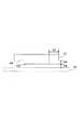
これを、図7を用いて説明する。モールド701は、第1の表面702、第2の表面703を有する凸型の構造をしている。
それらの面の距離705は、何らかの手段で既知のものとなっている。
704は基板、706は第1の表面と基板の距離、707は計測領域である。For this reason, in
This will be described with reference to FIG. The
The
ところで上記特許文献1では、第2の表面と基板表面の距離を計測することにより、第1の表面と基板の距離が計測波長の4分の1波長以下になっても計測できるとされている。
しかしながら、このギャップを計測する方法では、第2の表面に対向する位置に、第1の表面が無いことから、第1の表面と第2の表面の距離を、第1の表面と基板の距離を計測する光軸と同じにすることは難しい。
これは、パターン形成時の応力等による歪みや熱等による膨張が起こるナノインプリントにおいて重大である。
すなわち、第2の表面と基板表面の距離がわかったとしても、第1の表面と基板表面の正確な距離とはならない場合がある。
また、モールドと基板の距離計測を行う光学系と面内位置計測を行う光学系は別の構成となっている。特にナノインプリントはステッパー等の縮小露光と異なりモールドと加工パターンの大きさが1:1になるパターン形成装置である。
そのため、モールドの裏面より後方の位置においては空間的制約条件がステッパー等と比較して厳しくなる。
例えば、モールドの加工面のパターン領域は26×33mmで、光学系に使われる対物レンズはφ20mm程度で、それらの大きさは同じオーダーである。
距離計測を行う光学系と面内位置計測を行う光学系が別であれば、それらを同時に配置することは難しくなる。
そのような状態においては、温度変化や振動等によりモールドと基板の位置がずれることによる距離計測の誤差を防ぐことは難しい。By the way, in the said
However, in this method of measuring the gap, there is no first surface at a position facing the second surface, so the distance between the first surface and the second surface is the distance between the first surface and the substrate. It is difficult to make the same as the optical axis for measuring.
This is important in nanoimprint in which distortion due to stress or the like during pattern formation or expansion due to heat or the like occurs.
That is, even if the distance between the second surface and the substrate surface is known, the accurate distance between the first surface and the substrate surface may not be obtained.
Further, the optical system for measuring the distance between the mold and the substrate and the optical system for measuring the in-plane position have different configurations. In particular, nanoimprinting is a pattern forming apparatus in which the size of a mold and a processing pattern is 1: 1 unlike reduced exposure such as a stepper.
For this reason, the spatial constraint condition becomes stricter than that of a stepper or the like at a position behind the back surface of the mold.
For example, the pattern area of the processing surface of the mold is 26 × 33 mm, the objective lens used in the optical system is about φ20 mm, and their sizes are the same order.
If the optical system that performs distance measurement is different from the optical system that performs in-plane position measurement, it is difficult to arrange them simultaneously.
In such a state, it is difficult to prevent a distance measurement error due to a shift in the position of the mold and the substrate due to a temperature change, vibration, or the like.
本発明は、上記課題に鑑み、モールドの転写パターンが形成された加工面を含む表面と、被加工部材である基板との間の空間的位置関係を正確に計測することが可能となるパターン形成装置、パターン形成方法の提供を目的とする。In view of the above problems, the present invention provides a pattern formation that can accurately measure a spatial positional relationship between a surface including a processing surface on which a transfer pattern of a mold is formed and a substrate that is a workpiece. apparatus, and an object thereof is to providea patterninghow.
本発明は上記課題を解決するため、つぎのように構成したパターン形成装置、パターン形成方法を提供するものである。
本発明は、モールドと被加工部材とを合わせて、モールドの加工面に形成されたパターンを、前記被加工部材に転写するパターン形成装置を、つぎのように構成する。
すなわち、前記モールドの加工面から後退した位置にあり、且つ前記モールドの加工面と対向した計測基準面を介し、前記計測基準面と前記基板表面との間の距離を計測する。
そして、前記計測基準面と前記加工面の間の厚みと前記計測結果に基づいて、前記モールドの加工面と前記基板表面との間の距離を計測可能に構成した距離計測機構を有することを特徴としている。
前記距離計測機構は、
前記モールドの加工面と前記基板表面との間の距離を計測するために用いる距離計測用の光源と、
前記光源からの光を前記計測基準面と前記基板表面間に導くと共に、それらの反射光を分光器に導く光学系と、を備え、
前記距離計測機構の光学系は、反射前の光と反射後の光の両方が共通の光学系を 透過するように構成され、かつ、前記モールドと前記被加工部材の、面内の位置合わせを行うための光学系と同軸に構成されている。
また、本発明のパターン形成装置は、前記距離計測機構が、前記計測したデーター、モールドや樹脂層の屈折率を記憶させる記憶手段を備えていることを特徴としている。
また、本発明のパターン形成装置は、前記分光器は、前記光学系に導かれた光を分光することを特徴としている。
また、本発明のパターン形成装置は、前記距離計測用の光源が、ブロードバンド光を放出する光源であることを特徴としている。
また、本発明のパターン形成装置は、モールドと被加工部材を合わせて、モールドの加工面に形成されたパターンを、前記被加工部材に転写するパターン形成装置をつぎのように構成する。
すなわち、前記モールドの加工面から後退した位置にあり、且つ前記モールドの加工面と対向した計測基準面を介し、前記計測基準面と前記基板表面との間の距離を計測する。
そして、前記計測基準面と加工面の間の厚みと前記計測結果に基づいて、前記モールドの加工面と前記基板表面との間の距離を計測する距離計測機構を有している。
そして、前記距離計測機構は、ブロードバンド光を放出する光源である第1の光源と、該第1の光源と異なる第2の光源を有し、
前記加工面と基板表面に設けられた樹脂層表面が離れている状態において前記第1の光源による計測を行い、
前記加工面と基板表面に設けられた樹脂層表面が接触している状態において前記第2の光源による計測を行って、前記モールドの加工面と前記基板表面との間の距離を計測可能に構成したことを特徴としている。
また、本発明のパターン形成装置は、前記光学系は、前記計測基準面と基板までの距離よりコヒーレンス長の長い計測系であることを特徴としている。
また、本発明のパターン形成方法は、モールドと被加工部材を合わせて、モールドの加工面に形成されたパターンを、前記被加工部材に転写するパターン形成方法であって、
前記モールドの加工面から後退した位置にあり、且つ前記モールドの加工面と対向した計測基準面を介し、前記計測基準面と前記被加工部材を構成する基板表面との間の距離を計測し、
前記計測基準面と前記加工面の間の厚みと前記計測結果に基づいて、前記モールドの加工面と前記基板表面との間の距離を計測する距離計測工程を有し、
前記距離計測工程は、
ブロードバンド光を用い、前記加工面と基板表面に設けられた樹脂層表面が離れている状態において計測を行うブロードバンド光による計測工程と、
レーザー光を用い、前記加工面と基板表面に設けられた樹脂層表面を接触させた状態において計測を行うレーザー光による計測工程と、
ブロードバンド光による計測工程によって得た計測結果と、レーザー光による計測工程によって得た計測結果に基づいて、加工面と前記基板表面との間の距離を得る工程と、を含むことを特徴している。
また、本発明のパターン形成装置は、前記被加工部材は、前記基板表面に樹脂層を設けていることを特徴としている。
また、本発明のパターン形成装置は、前記モールドまたは前記被加工部材を、相対的に動かし加圧することにより転写することを特徴としている。
また、本発明のパターン形成装置は、前記距離計測と前記面内位置計測を行う光学系の開口数が異なることを特徴としている。
また、本発明のパターン形成装置は、前記距離計測機構の光学倍率と面内位置計測の光学倍率が異なることを特徴としている。
また、本発明は上記したブロードバンド光が、キセノン光源またはハロゲン光源であることを特徴としている。In order to solve the above problems, the present invention provides a pattern forming apparatus and a pattern forming method configured as follows.
According to the present invention, a pattern forming apparatus for combining a mold and a workpiece and transferring a pattern formed on the processing surface of the mold to the workpiece is configured as follows.
That is, the distance between the measurement reference surface and the substrate surface is measured via a measurement reference surface that is at a position retracted from the processing surface of the mold and faces the processing surface of the mold.
And a distance measuring mechanism configured to measure a distance between the processing surface of the mold and the substrate surface based on the thickness between the measurement reference surface and the processing surface and the measurement result. It is said.
The distance measuring mechanism is
A light source for distance measurement used to measure the distance between the processed surface of the mold and the substrate surface;
An optical system that guides light from the light source between the measurement reference plane and the substrate surface, and guides reflected light to a spectroscope,
The optical system of the distance measuring mechanism is configured so that both the light before reflection and the light after reflection pass through a common optical system, and aligns the mold and the workpiece to be processed in the plane. It is configured coaxially with the optical system for performing.
In the pattern forming apparatus according to the present invention, the distance measuring mechanism includes a storage unit that stores the measured data, the refractive index of the mold or the resin layer.
In the pattern forming apparatus of the present invention, the spectroscope splits the light guided to the optical system.
The pattern forming apparatus of the present invention is characterized in that the distance measuring light source is a light source that emits broadband light.
Moreover, the pattern forming apparatus of this invention comprises the pattern and the to-be-processed member which match | combines a mold and a to-be-processed member, and the pattern formed on the to-be-processed member is comprised as follows.
That is, the distance between the measurement reference surface and the substrate surface is measured via a measurement reference surface that is at a position retracted from the processing surface of the mold and faces the processing surface of the mold.
And it has a distance measurement mechanism which measures the distance between the processing surface of the mold and the substrate surface based on the thickness between the measurement reference surface and the processing surface and the measurement result.
The distance measuring mechanism includes a first light source that is a light source that emits broadband light, and a second light source that is different from the first light source,
In the state where the resin layer surface provided on the processing surface and the substrate surface is separated, measurement by the first light source,
The distance between the processed surface of the mold and the substrate surface can be measured by measuring with the second light source in a state where the processed surface and the resin layer surface provided on the substrate surface are in contact with each other. It is characterized by that.
In the pattern forming apparatus of the present invention, the optical system is a measurement system having a coherence length longer than a distance between the measurement reference plane and the substrate.
The pattern forming method of the present invention is a pattern forming method in which a mold and a workpiece are combined, and a pattern formed on the processing surface of the mold is transferred to the workpiece.
The distance between the measurement reference surface and the substrate surface constituting the workpiece is measured via a measurement reference surface that is in a position retracted from the processing surface of the mold and faces the processing surface of the mold,
A distance measuring step of measuring a distance between the processing surface of the mold and the substrate surface based on a thickness between the measurement reference surface and the processing surface and the measurement result;
The distance measuring step includes
Using broadband light, a measurement process with broadband light that performs measurement in a state where the processed surface and the resin layer surface provided on the substrate surface are separated from each other;
Using a laser beam, a measurement step with a laser beam that performs measurement in a state where the processed surface and the resin layer surface provided on the substrate surface are in contact with each other;
And a step of obtaining a distance between the processing surface and the substrate surface based on a measurement result obtained by the measurement step using broadband light and a measurement result obtained by the measurement step using laser light..
Also, the pattern forming apparatus of the present invention, the workpiece is characterized in that the resin layer is provided on the substrate surface.
Further, the pattern forming apparatus of the present invention is characterized in that the mold or the workpiece is moved by relatively moving and pressurizing.
Moreover, the pattern forming apparatus of the present invention is characterized in that the numerical aperture of the optical system that performs the distance measurement and the in-plane position measurement is different.
The pattern forming apparatus of the present invention is characterized in that the optical magnification of the distance measuring mechanism is different from the optical magnification of in-plane position measurement.
Further, the present invention is characterized in that the broadband light described above is a xenon light source or a halogen light source.
本発明によれば、モールドの転写パターンが形成された加工面を含む表面と、被加工部材である基板との間の空間的な位置関係を正確に計測することが可能となる。
また、面内位置計測を同時に行うことにより、距離計測を行う領域がずれないように制御し、さらに高精度の計測が可能となる。
これにより、高精細な加工が可能となるパターン形成装置、パターン形成方法を実現することができる。
ADVANTAGE OF THE INVENTION According to this invention, it becomes possible to measure correctly the spatial positional relationship between the surface including the process surface in which the transfer pattern of the mold was formed, and the board | substrate which is a to-be-processed member.
In addition, by performing in-plane position measurement at the same time, control is performed so that the area for distance measurement does not shift, and more accurate measurement is possible.
Thus, the possibility is high definition processing and made patterning device, it is possible to realizea pattern forminghow.
上記構成によれば、モールドの転写パターンが形成された加工面を含む表面と、被加工部材である基板との間の空間的な位置関係を保持できるため正確に計測することが可能となる。
それは、上記した従来例とは異なり、上記したようにモールドの加工面と対向した位置に計測域を構成したことで、モールドの加工表面と基板表面の距離を同軸で測定可能とされていることによる。
このような構成によれば、モールドの表面と基板表面が樹脂に接触した状態にあっても、モールドの加工表面と基板表面の距離を直接測定することができる。
その結果、残膜層の膜厚の制御が正確におこなうことができ、所望の深さのパターンを得ることが容易になる。
また、このような構成によれば、モールドにパターン形成時の応力等による歪みや熱等による膨張が起こった場合においても、モールドの厚みを測った同じ光軸でモールドの表面と基板表面の距離を正確に測定することができる。
その結果、残膜層の膜厚を正確に制御可能となり、エッチング時のエッチング時間を正確に計算することができ、所望の深さのパターンを得ることができる。
また、以上の技術は、半導体製造技術、フォトニッククリスタル等の光学素子やμ−TAS等のバイオチップの製造技術等として利用することができる。According to the above configuration, since the spatial positional relationship between the surface including the processed surface on which the transfer pattern of the mold is formed and the substrate that is the member to be processed can be maintained, accurate measurement can be performed.
Unlike the conventional example described above, it is possible to measure the distance between the mold processing surface and the substrate surface coaxially by configuring the measurement area at the position facing the mold processing surface as described above. by.
According to such a configuration, even when the mold surface and the substrate surface are in contact with the resin, the distance between the processed surface of the mold and the substrate surface can be directly measured.
As a result, the film thickness of the remaining film layer can be accurately controlled, and a pattern having a desired depth can be easily obtained.
In addition, according to such a configuration, even when distortion due to stress or the like during pattern formation or expansion due to heat or the like occurs in the mold, the distance between the mold surface and the substrate surface on the same optical axis that measured the thickness of the mold. Can be measured accurately.
As a result, the film thickness of the remaining film layer can be accurately controlled, the etching time during etching can be accurately calculated, and a pattern having a desired depth can be obtained.
Moreover, the above technique can be used as a semiconductor manufacturing technique, a manufacturing technique of an optical element such as a photonic crystal, or a biochip such as μ-TAS.
以下に、本発明の実施例について説明する。
[実施例1]
実施例1においては、本発明を適用したパターン形成装置の構成例について説明する。
図1に、本実施例1におけるパターン形成装置の構成例を示す。
図1において、101は露光光源、102はモールド保持部、103はワーク保持部、104はワーク加圧機構、105は面内移動機構である。
106は光学系、107は計測用光源、108はビームスプリッター、109は分光器、110は撮像素子、111は解析機構である。112はインプリント制御機構である。
113はモールド、114は光硬化樹脂、115は基板である。Examples of the present invention will be described below.
[Example 1]
In the first embodiment, a configuration example of a pattern forming apparatus to which the present invention is applied will be described.
FIG. 1 shows a configuration example of a pattern forming apparatus according to the first embodiment.
In FIG. 1, 101 is an exposure light source, 102 is a mold holding part, 103 is a work holding part, 104 is a work pressing mechanism, and 105 is an in-plane moving mechanism.
106 is an optical system, 107 is a measurement light source, 108 is a beam splitter, 109 is a spectroscope, 110 is an image sensor, and 111 is an analysis mechanism.
113 is a mold, 114 is a photo-curing resin, and 115 is a substrate.
本実施例のパターン形成装置は、露光光源101、モールド保持部102、ワーク保持部103、ワーク加圧機構104、面内移動機構105、インプリント制御機構112、ギャップ計測機構、等により構成される。
ここで、ワークとは被加工部材を構成する光硬化樹脂の塗布された基板である。モールド保持部102は、真空チャック方式等によってモールド113のチャッキングを行う。
ワークは面内移動機構105により所望の位置に移動することができ、ワーク加圧機構104によりワークの高さの調整および加圧を行うことができる。
なお、ワーク加圧機構104はエンコーダーによって高さ方向の位置をモニターすることができる。
このエンコーダーの精度は100nm以下であることが望ましい。ワークの位置移動、加圧、露光等の制御はインプリント制御機構112によって行う。
また、ここでは省略されているが、面内の位置合わせを行うための検出系なども備えている。
基板115はモールド113に対向する位置に置かれ、基板には光硬化樹脂114が塗布されている。
なお、ここでの塗布方法はスピンコート法である。The pattern forming apparatus according to the present embodiment includes an exposure
Here, the workpiece is a substrate coated with a photocurable resin that constitutes a workpiece. The
The workpiece can be moved to a desired position by the in-
The
The accuracy of this encoder is desirably 100 nm or less. The
Although omitted here, a detection system for performing in-plane alignment is also provided.
The
The coating method here is a spin coating method.
つぎに、本実施例のギャップ計測機構について説明する。
本実施例のギャップ計測機構は、光学系106、計測用光源107、ビームスプリッター108、分光器109、撮像素子110、解析機構111を有している。
ここで、計測用光源107は、例えば400nm−800nmのブロードバンド光等の光を出す光源で構成されている。
計測用光源107から出た光は光学系106を通り、モールド113、光硬化樹脂114、基板115に到達する。
この光はモールド113、光硬化樹脂114、基板115の間で干渉し、その干渉光は光学系106に戻り、分光器109に到達する。
分光器109によって分光された光は、撮像素子110により観察される。撮像素子110はラインセンサーなどである。
解析機構111は屈折率や計測したデーターを予め記憶する記憶デバイスを備え、さらに、撮像素子110からの信号の処理を行う。
なお、ギャップ計測機構と面内の位置合わせを行うための検出系を同軸にすることもできる。
ここで、光学系に更なるビームスプリッターを設けることにより、ギャップ計測を行う光学系、面内の位置合わせを行う光学系に分岐させる。
この方法により、面内およびギャップの計測をそれぞれ独立にするより少ない光学系で行うことができる。Next, the gap measuring mechanism of this embodiment will be described.
The gap measurement mechanism of this embodiment includes an
Here, the
The light emitted from the
This light interferes between the
The light separated by the
The
The gap measurement mechanism and the detection system for performing in-plane alignment can be coaxial.
Here, by providing a further beam splitter in the optical system, the optical system is branched to an optical system that performs gap measurement and an optical system that performs in-plane alignment.
By this method, in-plane and gap measurement can be performed with fewer optical systems that are independent of each other.
つぎに、光の干渉により膜の厚みやギャップの距離を測定する原理について説明する。
まず、ナローバンド(狭帯域)の光源を使う方法について説明する。
このような光源として、レーザー、LED等がある。またブロードバンド光源にフィルターを用いても良い。
ここで薄膜の厚さをd、屈折率をnとしたときに、薄膜の両端で反射した光が干渉した場合を考える。
強度が小さくなる波数kmoおよび波長λmoは任意の整数mを用いて次の関係式を満たす。なお、ここで波数は単位長さあたりの波の数とする。
First, a method using a narrow band light source will be described.
Such light sources include lasers and LEDs. A filter may be used for the broadband light source.
Here, a case is considered where the light reflected at both ends of the thin film interferes when the thickness of the thin film is d and the refractive index is n.
The wave number kmo and the wavelength λmo with decreasing intensity satisfy the following relational expression using an arbitrary integer m. Here, the wave number is the number of waves per unit length.
また、強度が大きくなる波数kmeおよび波長λmeは次の関係式を満たす。
このように、強度は波数および波長によって周期的に変わる。
従って、光の強度は半波長分の距離ごとに周期的に変化する。
例えば波長600nm,n=1.5であれば、周期は200nmとなる。
この周期以上の距離を測定するには例えば精度100nm程度のエンコーダーを用いる。さらに、モールド表面と基板表面の初期位置が合わせて100nm以内の誤差であれば、
モールドと基板の絶対的な距離を測定することができる。Thus, the intensity varies periodically with wave number and wavelength.
Therefore, the intensity of light periodically changes for each half wavelength.
For example, if the wavelength is 600 nm and n = 1.5, the period is 200 nm.
For example, an encoder having an accuracy of about 100 nm is used to measure a distance longer than this period. Furthermore, if the initial position of the mold surface and the substrate surface is within 100 nm,
The absolute distance between the mold and the substrate can be measured.
つぎに、本実施例の計測用光源107のように、ブロードバンド(広帯域)の光源を用いることで、膜の厚さやギャップの距離の絶対値を求める方法について説明する。なお、このような光源として、ハロゲン光源やキセノン光源等がある。
図2に、1層の膜において、屈折率および厚みがそれぞれ異なっている時の波数に対する強度の模式図を示す。
図2(a)は山と谷が計測波数内に3つある状態、図2(b)は山と谷が計測波数内に2つある状態、図2(c)は山と谷が計測波数内に1つしかない状態を示す図である。Next, a method of obtaining the absolute values of the film thickness and the gap distance by using a broadband light source like the
FIG. 2 shows a schematic diagram of the intensity with respect to the wave number when the refractive index and thickness are different in a single layer film.
2A shows a state where there are three peaks and valleys within the measured wave number, FIG. 2B shows a state where there are two peaks and valleys within the measured wave number, and FIG. 2C shows a state where the peaks and valleys are measured wave number. It is a figure which shows the state which has only one in it.
屈折率はそれぞれna、nb、nc、膜の厚さはそれぞれda、db、dcである。201、202は近接する山と山の間隔でそれぞれ1/2nada、1/2nbdbである。203は近接する山と谷で1/4ncdcである。
この結果、フーリエ変換などの周波数解析、山と谷や山と山のピーク検出から光学距離ndを計算することができることが分かる。
なお、計測できる波数の最小値をkL=1/λL、最大値をkM=1/λMとする。屈折率は説明を簡単にするために波長に依存しないものとする。
また、ここでは例えば上端を透過して、下端で反射した光が上端、下端で再度反射して出てくるような多重反射の影響も考慮しない。
ここで具体的な数値例をあげると例えばda=800nm,db=500nm,dc=300nmでn=1.4,kL=1/400,kM=1/800とした場合である。
この方法においては膜の厚さが薄くなるほど山と谷の数が減っていく。
この場合測定できる厚さの最小はm=0の時で以下の式で表される。
As a result, it can be seen that the optical distance nd can be calculated from frequency analysis such as Fourier transform and peak and valley detection.
Note that the minimum value of the wave number that can be measured is kL = 1 / λL , and the maximum value is kM = 1 / λM. The refractive index is not dependent on wavelength for the sake of simplicity.
Further, here, for example, the influence of multiple reflections in which light transmitted through the upper end and reflected at the lower end is reflected again at the upper and lower ends is not considered.
Here, specific numerical examples are given, for example, when da = 800 nm, db = 500 nm, dc = 300 nm, n = 1.4, kL = 1/400, and kM = 1/800. .
In this method, the number of peaks and valleys decreases as the film thickness decreases.
In this case, the minimum thickness that can be measured is expressed by the following equation when m = 0.
先ほどの数値例を適用すると71nmが最小である。
つぎに、2層の場合を考える。この場合、それぞれの端面で反射する。例えば2層の厚さがda,dbであるとし、十分帯域の広い光を用いれば、図2(a)、(b)のスペクトルに定数を乗じた和が得られる。
これを周波数解析することによってnada,nbdb,nada+nbdbの3通りの位置にピークが発生する。
さらに、3層の場合は図2(a)、(b)、(c)のスペクトルの和で、周波数解析をすることによりnada,nbdb,ncdc,nada+nbdb,nbdb+ncdc,nada+nbdb+ncdcの6通りのピークが現れる。なお、計測波長の光学距離に換算して4分の1波長より短い距離を計測する場合には、前もって計算した値と比較することによって測定することが可能である。さらに、計測方法はエリプソメトリーを使う方法であってもよい。Applying the numerical example above, 71 nm is the minimum.
Next, consider the case of two layers. In this case, the light is reflected at each end face. For example, the thickness of the two layers is to be da, db, by using the wide light enough bandwidth, FIG. 2 (a), the resulting sum multiplied by the constants in the spectrum of (b).
Na da by which the frequency analysis, nb db, the peak occurs in the position of three ways ofn a d a + n b d b.
Furthermore, in the case of a three-layer Fig 2 (a), (b) , the sum of the spectrum (c), na da by frequencyanalysis, n b d b, n c d c, n a da + n b d b, n b d b + n c d c, n a d a + n b d b + n c d peak of six ofc appear. In addition, when measuring a distance shorter than a quarter wavelength in terms of the optical distance of the measurement wavelength, the measurement can be performed by comparing with a value calculated in advance. Further, the measurement method may be a method using ellipsometry.
つぎに、本実施例のギャップ計測方法について説明する。
この方法に好適な条件はモールドの裏面から基板の表面までの光学距離が光のコヒーレンス長より短いことである。なおコヒーレンス長は以下の式で与えられる。
A suitable condition for this method is that the optical distance from the back surface of the mold to the front surface of the substrate is shorter than the coherence length of the light. The coherence length is given by the following equation.
例えば、つぎのような式であれば、コヒーレンス長は16mmになる。モールドの厚さが6mmであれば、十分この条件を満たしている。
ここで、モールドと基板の位置と干渉光の関係について説明する。
図3に、本実施例におけるモールドの裏面を使って測定する方法を説明する。
モールドに入射したブロードバンド光はモールドの裏面301、モールド第1の表面302、樹脂表面303、基板表面304で反射する。
そして、それぞれが干渉305し計測系へ戻る。Here, the relationship between the position of the mold and the substrate and the interference light will be described.
FIG. 3 illustrates a method for measuring using the back surface of the mold in this embodiment.
The broadband light incident on the mold is reflected by the
And each interferes 305 and returns to a measurement system.
図3(a)はモールドと樹脂が接触していない状態である。ここでモールドの裏面−モールド第1の表面距離d1、モールド第1の表面−樹脂表面距離d2、樹脂表面−基板表面距離d3とする。
この場合干渉光を分光し周波数解析を行うとn1d1,n2d2,n3d3,n1d1+n2d2,n2d2+n3d3,n1d1+n2d2+n3d3の6通りのピークが現れる。ここでモールド、空気、光硬化樹脂の屈折率は加圧中に変化しないので予め記憶させたデーターを必要な時に参照する。
この結果d1,d2,d3をそれぞれ計算することができる。
図3(b)はモールドと樹脂が接触している場合である。
このとき、モールドと樹脂の屈折率が近いためモールドの加工面において反射がほとんど起こらない。この場合n1d1+n3d3にピークが現れる。FIG. 3A shows a state where the mold and the resin are not in contact. Here, the back surface of the mold—the mold first surface distance d1 , the mold first surface—the resin surface distance d2 , and the resin surface—the substrate surface distance d3 .
In this case, when the interference light is dispersed and frequency analysis is performed, n1 d1 , n2 d2 , n3 d3 , n1 d1 + n2 d2 , n2 d2 + n3 d3 , n1 d1 + n Six peaks of2 d2 + n3 d3 appear. Here, since the refractive indexes of the mold, air, and photo-curing resin do not change during pressurization, data stored in advance is referred to when necessary.
As a result, d1 , d2 , and d3 can be calculated.
FIG. 3B shows a case where the mold and the resin are in contact.
At this time, since the refractive indexes of the mold and the resin are close, almost no reflection occurs on the processed surface of the mold. In this case, a peak appears at n1 d1 + n3 d3 .
つぎに、モールドを基板に近づけながら計測するシーケンスを説明する。
まず、モールド裏面と基板表面の距離がコヒーレンス長以上である位置で、モールドの厚さd1を計測し解析機構に記憶させる。次にワーク加圧機構で近づけていく。この間、モールドと基板の距離のモニターはワーク加圧機構のエンコーダーで行う。
つぎに、コヒーレンス長以内でかつ樹脂に接触していない領域までモールドと基板を近づける。
この領域では周波数解析によりd1,d2,d3を計算することができる。
したがって、モールド第1の表面と基板表面の距離はd2+d3である。
さらに近づけていき、モールドと樹脂が接触した状態になる。
この領域ではピークがn1d1+n3d3に現れる。
ここで、予め計測したn1d1を減算することによってd3を計算することができ、この値がモールド第1の表面と基板表面の距離を得ることができる。
なお、予めn1d1を計測した光軸とモールドと基板の間隔を近づけていくときに計測する光軸とが同じであるため、精度の高い結果を得ることが可能である。Next, a sequence for measuring while bringing the mold close to the substrate will be described.
First, at a position where the distance between the mold back surface and the substrate surface is equal to or greater than the coherence length, the mold thickness d1 is measured and stored in the analysis mechanism. Next, it is moved closer by the work pressure mechanism. During this time, the distance between the mold and the substrate is monitored by the encoder of the work pressure mechanism.
Next, the mold and the substrate are brought close to a region within the coherence length and not in contact with the resin.
In this region, d1 , d2 , and d3 can be calculated by frequency analysis.
Therefore, the distance between the mold first surface and the substrate surface is d2 + d3 .
Further, the mold and the resin come into contact with each other.
In this region, a peak appears at n1 d1 + n3 d3 .
Here, d3 can be calculated by subtracting n1 d1 measured in advance, and this value can obtain the distance between the mold first surface and the substrate surface.
Since the optical axis to measure when brought closer spacing advance n1 optical axis and the mold and the substrate was measured d1 is the same, it is possible to obtain accurate results.
また、本実施例のシーケンスにおいて、モールドの第1の表面と基板表面が接してない場合、d2のみ変化するためn1d1,n3d3,の成分を減算することによって計算を簡略化することができる。
さらにまた、光源の強度スペクトルはフラットではない。そのため予め強度スペクトルを取っておき、計測光のスペクトルと強度スペクトルで除算することにより規格化をすることができる。その結果さらに精度の高い周波数解析を行うことができる。
さらに、ギャップ計測機構を3本以上備えることによりモールドと基板の傾きを検出でき、モールドと基板の平行度を合わせることが可能になる。
また、モールドと基板の平行度を合わせる別の方法として光学系を面内に駆動する駆動機構を設けることによって、計測光を面内に移動しながらギャップを計測することができる。例えば原点、X方向に移動した点、Y方向に移動した点にてそれぞれギャップを計測する。
この結果、モールドと基板の傾きを検出することができ、平行度を合わせることが可能である。Further, in the sequence of this embodiment, when the first surface of the mold is not in contact with the substrate surface, only d2 changes, so that the calculation is simplified by subtracting the components of n1 d1 and n3 d3 . Can be
Furthermore, the intensity spectrum of the light source is not flat. Therefore, normalization can be performed by taking an intensity spectrum in advance and dividing by the spectrum of the measurement light and the intensity spectrum. As a result, more accurate frequency analysis can be performed.
Further, by providing three or more gap measuring mechanisms, it is possible to detect the inclination of the mold and the substrate, and to match the parallelism of the mold and the substrate.
Further, by providing a driving mechanism for driving the optical system in the plane as another method for matching the parallelism between the mold and the substrate, the gap can be measured while moving the measuring light in the plane. For example, the gap is measured at the origin, the point moved in the X direction, and the point moved in the Y direction.
As a result, the inclination of the mold and the substrate can be detected, and the parallelism can be adjusted.
本実施例のパターン形成装置におけるモールドの構成を図4に示す。
401はモールド本体を形成している第1の透明部材である。
この透明部材は、つぎのような部材等によることができる。
401 is a first transparent member forming a mold body.
The transparent member can be the following member.
図4(a)は、モールドの第1の表面とモールドの第1の裏面が対向している点線で囲んだ位置に計測域がある場合の形態を示す図である。
図4(a)において、402はモールドの第1の表面、403はモールドの第1の裏面、404はモールドの第2の表面である。
モールドの第2の表面404は第1の表面402より裏面側に後退した位置にある。
また、406の点線で囲んだ領域はギャップの計測領域である。
また、図4(b)は、第1の表面と第2の裏面が対向している点線で囲んだ位置に計測域がある場合である。
図4(b)において、405はモールドの第2の裏面であり、第1の裏面403よりモールドの第1の表面402側にある。
この構成は、コヒーレンス長が図4(a)のモールドの表面と裏面の距離より短い場合に有効である。
また、図4(c)は、図4(b)の別の形態であり、点線で囲んだ計測域の部分が窪んでいる位置に構成されている。
また、図4(d)は、第1の透明部材と第2の透明部材からなる構成である。
図4(d)において、407は第2の透明部材であり、408は第2の透明部材と第1の透明部材の境界を示す。
第1の透明部材と第2の透明部材では屈折率が異なっており、かつ光硬化樹脂のそれとも異なっている。
この時の第2の透明部材は、つぎのような部材等によることができる。
In FIG. 4A,
The
An area surrounded by a dotted
FIG. 4B shows a case where the measurement area is at a position surrounded by a dotted line where the first front surface and the second back surface face each other.
In FIG. 4B,
This configuration is effective when the coherence length is shorter than the distance between the front surface and the back surface of the mold in FIG.
Moreover, FIG.4 (c) is another form of FIG.4 (b), and is comprised in the position where the part of the measurement area enclosed with the dotted line is depressed.
FIG. 4D shows a configuration composed of a first transparent member and a second transparent member.
In FIG.4 (d), 407 is a 2nd transparent member, 408 shows the boundary of a 2nd transparent member and a 1st transparent member.
The first transparent member and the second transparent member have different refractive indexes and are different from those of the photo-curing resin.
The second transparent member at this time can be the following member.
計測域は第1の表面402と透明部材の境界面408が対向している位置にある。
この構成では第2の透明部材の厚みは、光学距離で計測波長の4分の1以上の長さである。
図4(e)は、図4(d)の別の形態であり、第2の透明部材407に第1の表面402と第2の表面404が含まれる場合である。
なお、計測域の第1の表面、第2の裏面、当面部材間の境界面は平面であることがより望ましい。The measurement area is at a position where the
In this configuration, the thickness of the second transparent member is not less than a quarter of the measurement wavelength in terms of optical distance.
FIG. 4E shows another form of FIG. 4D, in which the second
It is more preferable that the first surface, the second back surface, and the boundary surface between the members in the measurement area are flat surfaces.
[実施例2]
実施例2においては、実施例1とは異なりコヒーレンス長がモールドの厚みより短い時に好適な構成例について説明する。
図5に、本実施例における第1の透明部材と第2の透明部材を有するモールドで測定する方法を説明する図を示す。
実施例1との共通部分の説明は省略し、差異のある部分についてのみ説明する。図5において、501はモールド第1の表面、502は透明部材間の境界面、503は樹脂表面、504は基板表面、505はブロードバンド光による干渉である。
本実施例の実施例1との差異は、コヒーレンス長がモールドの厚みより短い時に適用され
ることである。[Example 2]
In the second embodiment, unlike the first embodiment, a configuration example suitable when the coherence length is shorter than the mold thickness will be described.
In FIG. 5, the figure explaining the method to measure with the mold which has the 1st transparent member and 2nd transparent member in a present Example is shown.
Description of common parts with the first embodiment is omitted, and only differences are described. In FIG. 5, 501 is a mold first surface, 502 is a boundary surface between transparent members, 503 is a resin surface, 504 is a substrate surface, and 505 is interference by broadband light.
The difference between the present embodiment and the first embodiment is that it is applied when the coherence length is shorter than the thickness of the mold.
例えば、つぎのような式であれば、コヒーレンス長は3.2mmである。
このような場合は、図4(d)、(e)のようなモールドを使うことが有効であり、この時の検出の方法について、つぎに説明する。なお、計測可能な範囲は第2の裏面405から基板の距離または透明部材間の境界面408から基板の距離がコヒーレンス長以内のところである。In such a case, it is effective to use a mold as shown in FIGS. 4D and 4E, and the detection method at this time will be described next. The measurable range is where the distance from the
ここで、モールドと基板の位置と干渉光の関係について説明する。
モールドに入射したブロードバンド光はモールドにおける上記境界面502、樹脂表面503、基板表面504で反射する。
それぞれが干渉505し計測系へ戻る。
図5(a)はモールドと樹脂が接触していない状態である。
ただし、モールドの第1の表面−境界面距離d1、モールドの第1の表面−樹脂表面距離d2、樹脂表面−基板表面距離d3である。
この場合干渉光を分光し周波数解析を行うと実施例1と同様にn1d1,n2d2,n3d3,n1d1+n2d2,n2d2+n3d3,n1d1+n2d2+n3d3の6通りのピークが現れる。
これらのピークから屈折率のデーターを参照することによってd1,d2,d3をそれぞれ計算することができる。
したがって、モールド第1の表面と基板表面の距離はd2+d3である。
図5(b)はモールドと樹脂が接触している場合である。
このときモールドと樹脂の屈折率が違うためモールドの第1の表面においても反射が起こる。したがって、ピークはn1d1+n3d3に現れる。
ここで、予め計測したn1d1を減算することによってd3を計算することができ、この計算により得た値がモールド第1の表面と基板表面の距離となる。Here, the relationship between the position of the mold and the substrate and the interference light will be described.
The broadband light incident on the mold is reflected by the
Each interferes 505 and returns to the measurement system.
FIG. 5A shows a state where the mold and the resin are not in contact.
However, the first surface-interface distance d1 of the mold, the first surface-resin surface distance d2 of the mold, and the resin surface-substrate surface distance d3 .
In this case, when the interference light is dispersed and frequency analysis is performed, n1 d1 , n2 d2 , n3 d3 , n1 d1 + n2 d2 , n2 d2 + n3 d3 , as in the first embodiment. , N1 d1 + n2 d2 + n3 d3 appear.
From these peaks, d1 , d2 , and d3 can be calculated by referring to the refractive index data.
Therefore, the distance between the mold first surface and the substrate surface is d2 + d3 .
FIG. 5B shows the case where the mold and the resin are in contact.
At this time, since the refractive indexes of the mold and the resin are different, reflection occurs also on the first surface of the mold. Therefore, the peak appears at n1 d1 + n3 d3 .
Here, d3 can be calculated by subtracting n1 d1 measured in advance, and the value obtained by this calculation is the distance between the first surface of the mold and the substrate surface.
[実施例3]
実施例3においては、実施例1、実施例2と異なり、コヒーレンス長がモールドの厚みより短く、かつモールドに第2の透明部材を設けることができない時に好適な構成例について説明する。
図6に、本実施例における樹脂に接触する前後で異なる光源を用いる測定方法を説明する図を示す。
実施例1、2との共通部分の説明は省略し、差異のある部分についてのみ説明する。
図6において、602はモールド第1の表面、603は樹脂表面、604は基板表面である。また、605はブロードバンド光による干渉、606はレーザーによる干渉を示している。
本実施例と実施例1、実施例2との差異は、コヒーレンス長がモールドの厚みより短く、かつモールドに第2の透明部材を設けることができない時に適用されることである。
このような場合には、図4(a)のようなモールドが用いられる。[Example 3]
In the third embodiment, unlike the first and second embodiments, a configuration example that is suitable when the coherence length is shorter than the thickness of the mold and the second transparent member cannot be provided in the mold will be described.
In FIG. 6, the figure explaining the measuring method using a different light source before and after contacting the resin in a present Example is shown.
Description of the common part with Example 1, 2 is abbreviate | omitted, and only a different part is demonstrated.
In FIG. 6, 602 is a mold first surface, 603 is a resin surface, and 604 is a substrate surface.
The difference between this example and Example 1 and Example 2 is that it is applied when the coherence length is shorter than the thickness of the mold and the second transparent member cannot be provided in the mold.
In such a case, a mold as shown in FIG. 4A is used.
ここで、モールドと基板の位置と干渉光の関係について説明する。
モールドに入射したブロードバンド光はモールドの裏面601、モールドの第1の表面602、樹脂表面603、基板表面604で反射する。
それぞれが干渉605し計測系へ戻る。図6(a)はモールドと樹脂が接触していない状態である。
干渉光を分光し周波数解析を行うとn2d2,n3d3,n2d2+n3d3の3通りのピークが現れる。
これは実施例1と異なるが、これはモールドの厚みがコヒーレンス長より長いためモール
ドの厚さの干渉を検出できないからである。
これらのピークから屈折率のデーターを参照することによってd2,d3をそれぞれ計算することができる。
したがって、モールド第1の表面と基板表面の距離はd2+d3である。この計測方法は樹脂に接触するまでこの計測をすることができ、接触した位置をdcとする。
図6(b)はモールドと樹脂が接触している場合である。
この状態ではコヒーレンス長の長いレーザー光によるモールド裏面の反射と基板表面の干渉光を観察する。モールドが基板表面に近づくにつれ、この干渉光の強度は正弦波的に変化する。レーザー光の波長をλとすれば、その周期はλ/2nとなる。
したがって、周波数の強度および強度の山の数をカウントすることによって移動距離Lを測定することができる。
この結果モールドの第1の表面と基板表面の距離はdc−Lで与えられる。Here, the relationship between the position of the mold and the substrate and the interference light will be described.
Broadband light incident on the mold is reflected by the
Each interferes 605 and returns to the measurement system. FIG. 6A shows a state where the mold and the resin are not in contact.
When the interference light is dispersed and the frequency analysis is performed, three peaks of n2 d2 , n3 d3 , n2 d2 + n3 d3 appear.
This is different from the first embodiment because the mold thickness is longer than the coherence length and interference of the mold thickness cannot be detected.
D2 and d3 can be calculated from these peaks by referring to the refractive index data.
Therefore, the distance between the mold first surface and the substrate surface is d2 + d3 . The measuring method may be the measurement until it contacts the resin, the contact position and dc.
FIG. 6B shows the case where the mold and the resin are in contact.
In this state, the reflection on the back side of the mold by the laser beam having a long coherence length and the interference light on the substrate surface are observed. As the mold approaches the substrate surface, the intensity of this interference light changes sinusoidally. If the wavelength of the laser beam is λ, the period is λ / 2n.
Therefore, the moving distance L can be measured by counting the frequency intensity and the number of intensity peaks.
As a result, the distance between the first surface of the mold and the substrate surface is given by dc -L.
[実施例4]
実施例4においては、モールド加工面と基板表面の距離計測(Z)および面内位置計測(XYθ)を行う光学系の一部を同軸にした構成例について説明する。図8(a)は本実施例の光学系で、撮像素子801、光源802、第1の結像系805、分光器810等からなる。
光源から出た光は第1のビームスプリッター809、第1の結像光学系をとおり、モールド806および基板807に到達する。モールド及び基板で反射した光は第1の結像光学系に戻る。
第2のビームスプリッター808に到達した光はそれぞれ距離計測用の集光部803および面内位置計測用の撮像素子に分岐される。
集光部に到達した光はファイバー等の導波路によって分光器に到達する。また、撮像素子および集光部は第1の結像系の焦点付近における情報が結像する位置である。
なお、基板から第2のビームスプリッターまでの光軸804を距離計測系および面内位置計測系で共有している。
特に、ナノインプリントではモールドと加工パターンの大きさが1:1になる方法である。そのためモールドの裏面より後方には空間を十分確保することが難しいという制約がある。
すなわち、距離計測を行う光学系と面内位置計測を行う光学系が別であれば、これらを同時にモールドの裏面より後方に配置することは難しいのはもちろんのこと、距離計測と面内位置計測を同時に測定を行うことも難しい。
そのような状態においては、温度変化や振動等によりモールドと基板の位置がずれることによる距離計測の誤差を防ぐことは難しい。一方光学系を共有することによってその制約を回避できる。[Example 4]
In Example 4, a configuration example in which a part of an optical system that performs distance measurement (Z) and in-plane position measurement (XYθ) between the mold processing surface and the substrate surface is coaxial will be described. FIG. 8A shows an optical system of this embodiment, which includes an
Light emitted from the light source passes through the
The light that has reached the
The light reaching the condensing unit reaches the spectroscope through a waveguide such as a fiber. The image sensor and the light condensing unit are positions where information is formed near the focal point of the first imaging system.
The
In particular, in nanoimprinting, the size of the mold and the processing pattern is 1: 1. Therefore, there is a restriction that it is difficult to ensure a sufficient space behind the back surface of the mold.
In other words, if the optical system that performs distance measurement and the optical system that performs in-plane position measurement are separate, it is difficult to place them at the back of the mold at the same time, as well as distance measurement and in-plane position measurement. It is also difficult to measure at the same time.
In such a state, it is difficult to prevent a distance measurement error due to a shift in the position of the mold and the substrate due to a temperature change, vibration, or the like. On the other hand, the limitation can be avoided by sharing the optical system.
図8(b)に距離計測系の開口数(NA)と面内位置計測系のNAを変えるための構成を示す。
第2のビームスプリッターから集光部までの間に絞り811を有する構成である。
面内位置計測においてはNAが高いほど光学系の分解能が高くなり、位置計測の精度が上がる。一方距離計測においては、収差の影響を排除するためにNAを小さくする方が有利な場合がある。このような時に有効な構成である。
図8(c)に距離計測系の光学倍率と面内位置計測系の光学倍率を変えるための構成を示す。
第2のビームスプリッターから撮像素子までの間に第2の結像光学系812を有する。
面内計測においては、倍率が高いほど高精度の位置計測ができる場合がある。
一方距離計測系は収差の影響を排除するためNAは小さく、かつ光学系は少ない方が良い。このようなときに有利である。
図8(d)はモールド加工面と基板表面の傾き計測を行うための構成である。
結像位置において、集光部を光軸に対し垂直な平面で移動するための駆動機構を有する構成である。
集光部を平面移動させながら距離計測を行うことによってモールド加工面と基板表面の傾きを検出することができる。FIG. 8B shows a configuration for changing the numerical aperture (NA) of the distance measurement system and the NA of the in-plane position measurement system.
The
In the in-plane position measurement, the higher the NA, the higher the resolution of the optical system and the higher the accuracy of position measurement. On the other hand, in distance measurement, it may be advantageous to reduce NA in order to eliminate the influence of aberration. This is an effective configuration at such times.
FIG. 8C shows a configuration for changing the optical magnification of the distance measurement system and the optical magnification of the in-plane position measurement system.
A second imaging
In the in-plane measurement, the higher the magnification, the more accurate position measurement may be possible.
On the other hand, in order to eliminate the influence of aberration, the distance measurement system should have a small NA and few optical systems. This is advantageous.
FIG. 8D shows a configuration for measuring the inclination of the mold processing surface and the substrate surface.
This is a configuration having a drive mechanism for moving the condensing unit on a plane perpendicular to the optical axis at the imaging position.
By measuring the distance while moving the condensing unit in a plane, the inclination between the mold processing surface and the substrate surface can be detected.
ここで、集光部の構造を図9で説明する。
集光部はファイバー901および保持部材902から成り立っている。保持部材は不要な反射を抑える反射防止膜が施されている。
また、テーパーをつけて測定部に戻らないようにしていてもよい。
図9(b)は複数の開口903を有する部材904である。
図8(a)において集光部803とビームスプリッター808の間で、かつ像面に複数の開口部材を配置する。
直接開口部に複数のファイバーをつけて情報を捕らえ、それらを切り換えることによって、面内の複数の位置における距離を計測することが可能となる。この結果モールド加工面と基板表面の傾きを計算することができる。Here, the structure of the condensing part will be described with reference to FIG.
The condensing part is composed of a
Further, a taper may be provided so as not to return to the measurement unit.
FIG. 9B shows a
In FIG. 8A, a plurality of aperture members are arranged on the image plane between the
It is possible to measure distances at a plurality of positions in a plane by attaching a plurality of fibers directly to the opening and capturing information and switching them. As a result, the inclination of the mold processing surface and the substrate surface can be calculated.
モールド加工面と基板表面の距離計測および面内位置計測を同時に行うための空間的位置計測マーク領域について説明する。
なお、座標は図面のように紙面の裏から表の方向をz軸の正方向とし、光学系を通して観察した時の破線1004で囲まれた領域が光学系の視野である。
図10(a)はモールドと基板がほぼ所望の相対する位置にある。
空間的位置計測マーク領域は距離計測領域と面内位置計測領域からなる。まず、第1の距離計測領域1003について説明する。距離計測領域は点線で示される領域で、ここでは光学系の視野の中心位置である。A spatial position measurement mark area for simultaneously measuring the distance between the mold processing surface and the substrate surface and measuring the in-plane position will be described.
Note that, as shown in the drawing, the coordinate is defined as the positive direction of the z-axis from the back side of the drawing, and the area surrounded by the
In FIG. 10A, the mold and the substrate are almost at the desired opposite positions.
The spatial position measurement mark area includes a distance measurement area and an in-plane position measurement area. First, the first
次に、面内位置計測領域1005について説明する。
モールドマークは複数のモールドマーク構成要素1001がx方向に並んでおり、基板マークは複数の基板マークの構成要素1002がモールドマーク構成要素の間に並んでいる。
なお、モールドマークの構成要素と基板マークの構成要素の間隔が等間隔になった時にモールドと基板の面内位置が合ったと判断される。
この空間的位置計測マーク領域においては加工面の面内方向(x軸)と加工面に垂直な方向(z軸)の2軸の位置合わせが可能となる。Next, the in-plane
The mold mark includes a plurality of
It is determined that the in-plane positions of the mold and the substrate are aligned when the interval between the component of the mold mark and the component of the substrate mark is equal.
In this spatial position measurement mark region, it is possible to align two axes, the in-plane direction (x-axis) of the processing surface and the direction (z-axis) perpendicular to the processing surface.
図10(b)は図10(a)におけるAA’位置における断面図である。
モールドマークは凸構造の構成要素1006からなり、基板マークは凹構造の構成要素1007からなっている例である。
距離計測域において、モールドの加工面側はマークの凸構造と同じ高さであり、基板の表面側はマークの凸構造と同じ高さである。したがって特に境界領域が設けられていない。
図10(c)は図10(a)におけるAA’位置における断面図が、図10(b)に対してモールドの凸構造と基板の凸構造が逆の場合である。
なお、両方凸構造であっても良いし、両方凹構造であっても良い。
また、距離計測域においてはモールド側、基板側、共に凹構造であっても良いしどちらかが凹構造であっても良い。
図10(d)は距離計測領域と面内位置計測領域の一部が共有している構成1010となっている。
図10(e)は面内位置計測を2次元で行うことができるマークの構成である。距離計測を視野の中心で行える構成となっており、3軸の計測ができ、さらに、周囲1011の部分で距離計測を行うことによって、モールドの加工面と基板の表面の傾きを計測することができる。FIG. 10B is a cross-sectional view at the position AA ′ in FIG.
In this example, the mold mark is composed of a
In the distance measurement area, the processed surface side of the mold has the same height as the convex structure of the mark, and the surface side of the substrate has the same height as the convex structure of the mark. Therefore, no boundary area is provided.
FIG. 10C is a cross-sectional view at the position AA ′ in FIG. 10A, in which the convex structure of the mold and the convex structure of the substrate are opposite to those in FIG.
In addition, both convex structures may be sufficient and both concave structures may be sufficient.
In the distance measurement area, both the mold side and the substrate side may have a concave structure, or one of them may have a concave structure.
FIG. 10D shows a
FIG. 10E shows a mark configuration that can perform in-plane position measurement in two dimensions. The distance measurement can be performed at the center of the field of view, and the measurement of three axes can be performed, and further, the distance between the
次に、モールド加工面と基板表面の距離計測および面内位置計測を同時に行うための手順について説明する。
図11(a)は、図10(a)や図10(d)のマークの構成を用いて面内位置制御と距離制御の手順を示すものである。
3次元で位置合わせを行う場合には、このようなマークおよび光学系が2箇所以上ある。
まず、S1−1の工程にてモールドを基板に近づける。この時モーターのエンコーダーなどを用いる粗動で、例えばモールド加工面と基板表面の距離を数十マイクロメートル程度に設定する。
S1−2の工程でマークを選択する。S1−3の工程で距離計測を行い、S1−4の工程で条件(1)を満たすかどうか判定する。
条件(1)は所望の距離に対して数ナノメートル以内の誤差であることなどである。
条件(1)を満たさない場合はS1−5の工程で距離制御を行う。条件(1)満たすとS1−6の工程の面内位置計測を行う。S1−7の工程で、条件(2)を満たすかどうかを判定する。この時の条件とは数ナノメートル以内の誤差であるなどである。
条件(2)を満たさない場合はS1−8の工程で面内位置制御を行う。条件(2)を満たす場合はS1−9の工程で条件(3)の判定を行う。Next, the procedure for simultaneously measuring the distance between the mold processing surface and the substrate surface and measuring the in-plane position will be described.
FIG. 11A shows the procedure of in-plane position control and distance control using the mark configuration of FIG. 10A and FIG. 10D.
In the case of performing alignment in three dimensions, there are two or more such marks and optical systems.
First, the mold is brought close to the substrate in the step S1-1. At this time, for example, the distance between the mold processing surface and the substrate surface is set to about several tens of micrometers by coarse movement using an encoder of a motor.
A mark is selected in step S1-2. Distance measurement is performed in the process of S1-3, and it is determined whether or not the condition (1) is satisfied in the process of S1-4.
Condition (1) is that the error is within a few nanometers with respect to the desired distance.
When the condition (1) is not satisfied, the distance control is performed in step S1-5. When the condition (1) is satisfied, the in-plane position measurement in the step S1-6 is performed. In step S1-7, it is determined whether or not the condition (2) is satisfied. The condition at this time is an error within several nanometers.
If the condition (2) is not satisfied, the in-plane position control is performed in step S1-8. When the condition (2) is satisfied, the condition (3) is determined in the step S1-9.
このときの条件としては、例えば、つぎの(a)乃至(c)などの条件とすることができる。
(a)全てのマークを測定していない。
(b)全てのマークを測定し、さらにモールドを近づける必要がある。
(c)全てのマークを測定し、モールドの加工面と基板の表面の距離が最終的な値に到達した。
(a)の場合はS1−2に進み別のマークの測定を行う。
(b)の場合はS1−10へ進みモールドの加工面と基板表面の距離を近づける。このときの距離は数百〜数十nm程度の微動である。
(c)の場合は終了である。As conditions at this time, for example, the following conditions (a) to (c) can be used.
(A) Not all marks are measured.
(B) It is necessary to measure all marks and bring the mold closer.
(C) All marks were measured, and the distance between the processed surface of the mold and the surface of the substrate reached the final value.
In the case of (a), the process proceeds to S1-2, and another mark is measured.
In the case of (b), the process proceeds to S1-10 and the distance between the processed surface of the mold and the substrate surface is reduced. The distance at this time is a fine movement of about several hundred to several tens of nm.
In the case of (c), the process is finished.
図11(b)は図10(e)のようなマークを用い、3次元の位置合わせを一つのマークと一つの光学系で行う工程を示す。
まず、S2−1の移動(1)により図11(a)と同様モールドを基板に近づける。
次に、S2−2の工程で距離を計測する。このときの距離計測は複数箇所である。
次に、S2−3の工程において、モールドの加工面と基板表面の傾きを計算する。
次に、S2−4の工程において、判定を行う。この時の条件(1)は距離および傾きが数ナノメートル以内であることなどである。FIG. 11B shows a process of using a mark as shown in FIG. 10E to perform three-dimensional alignment with one mark and one optical system.
First, the mold is moved closer to the substrate as in FIG. 11A by the movement (1) of S2-1.
Next, the distance is measured in step S2-2. The distance measurement at this time is a plurality of places.
Next, in the step S2-3, the inclination between the processed surface of the mold and the substrate surface is calculated.
Next, determination is performed in step S2-4. The condition (1) at this time is that the distance and the inclination are within several nanometers.
なお、条件を満たさない場合は、S2−5の工程において、距離制御を行う。これに対して、条件を満たす場合はS2−6の工程へ進む。
S2−7の工程において、条件(2)の判定を行う。この時の条件は面内の誤差が数ナノメートル以内であることである。
この条件を満たさない場合は、S2−8の面内位置制御を行う。
条件を満たす場合は、S2−9の工程において、条件(3)の判定を行う。この時の条件はモールドの加工面と基板表面の距離が最終的な距離であるかどうかである。
これらを満たす場合は終了し、満たさない場合はS2−11へ進みモールドの加工面と基板表面の距離を近づける。
なお、2次元のマークであっても複数個のマークで、複数個の光学系で観察することによってさらに精度を上げることができる。If the condition is not satisfied, distance control is performed in step S2-5. On the other hand, if the condition is satisfied, the process proceeds to step S2-6.
In step S2-7, the condition (2) is determined. The condition at this time is that the in-plane error is within several nanometers.
If this condition is not satisfied, the in-plane position control in S2-8 is performed.
If the condition is satisfied, the condition (3) is determined in the step S2-9. The condition at this time is whether or not the distance between the processed surface of the mold and the substrate surface is the final distance.
If these conditions are satisfied, the process ends. If not, the process proceeds to S2-11 to reduce the distance between the processed surface of the mold and the substrate surface.
Even if it is a two-dimensional mark, the accuracy can be further improved by observing with a plurality of optical systems with a plurality of marks.
101:露光光源
102:モールド保持部
103:ワーク保持部
104:ワーク加圧機構
105:面内移動機構
106:光学系
107:計測用光源
108:ビームスプリッター
109:分光器
110:撮像素子
111:解析機構
112:インプリント制御機構
113:モールド
114:光硬化樹脂
115:基板
201:近接する山と山の間隔1/2nada
202:近接する山と山の間隔1/2nbdb
203:近接する山と谷の間隔1/4ncdc
301:モールド裏面、
302:モールド第1の表面
303:樹脂表面
304:基板表面
305:ブロードバンド光による干渉
401:モールド第1の透明部材
402:モールド第1の表面
403:モールド第1の裏面
404:モールド第2の表面
405:モールド第2の裏面
406:計測領域
407:モールド第2の透明部材
408:透明部材間の境界面
501:モールド第1の表面
502:透明部材間の境界面
503:樹脂表面
504:基板表面
505:ブロードバンド光による干渉
601:モールドの裏面
602:モールド第1の表面
603:樹脂表面
604:基板表面
605:ブロードバンド光による干渉
606:レーザーによる干渉
701:モールド
702:第1の表面
703:第2の表面
704:基板
705:第1の表面と第2の表面の距離
706:第1の表面と基板の距離
707:計測領域801:撮像素子
802:光源
803:集光部
804:光軸
805:第1の結像光学系
806:モールド
807:基板
808:第1のビームスプリッター
809:第2のビームスプリッター
810:分光器
811:絞り
812:第2の結像光学系
813:集光部駆動機構
901:ファイバー
902:ファイバー保持部
903:開口
904:複数の開口のある部材
1001:モールドマークの構成要素
1002:基板マークの構成要素
1003:第1の距離計測領域
1004:顕微鏡観察領域
1005:面内位置計測領域
1006:凸構造のモールドマークの構成要素
1007:凹構造の基板マークの構成要素
1008:凹構造のモールドマークの構成要素
1009:凸構造の基板マークの構成要素
1010:第2の距離計測領域
1011:第3の距離計測領域101: Exposure light source 102: Mold holding unit 103: Work holding unit 104: Work pressure mechanism 105: In-plane moving mechanism 106: Optical system 107: Measurement light source 108: Beam splitter 109: Spectrometer 110: Image sensor 111: Analysis mechanism 112: the imprint control mechanism 113: mold 114: photocurable resin 115: substrate 201: spacing crests adjacent 1 / 2na da
202: interval of the mountain and the mountain in the vicinity of 1 / 2nb db
203: Interval between adjacent peaks and
301: The back of the mold,
302: Mold first surface 303: Resin surface 304: Substrate surface 305: Interference by broadband light 401: Mold first transparent member 402: Mold first surface 403: Mold first back surface 404: Mold second surface 405: Mold second back surface 406: Measurement area 407: Mold second transparent member 408: Interface between transparent members 501: Mold first surface 502: Interface between transparent members 503: Resin surface 504: Substrate surface 505: interference by broadband light 601: back surface of mold 602: mold first surface 603: resin surface 604: substrate surface 605: interference by broadband light 606: interference by laser 701: mold 702: first surface 703: second Surface 704: substrate 705: distance between first surface and second surface 706: first surface 707: Measurement area 801: Image sensor 802: Light source 803: Condenser 804: Optical axis 805: First imaging optical system 806: Mold 807: Substrate 808: First beam splitter 809: Second beam splitter 810: Spectrometer 811: Aperture 812: Second imaging optical system 813: Condensing unit drive mechanism 901: Fiber 902: Fiber holding unit 903: Opening 904: Member 1001 having a plurality of openings 1001: Mold Mark component 1002: Substrate mark component 1003: First distance measurement region 1004: Microscope observation region 1005: In-plane position measurement region 1006: Convex structure mold mark component 1007: Concave structure substrate mark configuration Element 1008: Concavity mold mark component 1009: Convex substrate mark component 10 0: second distance measurement area 1011: third distance measurement area
Claims (12)
Translated fromJapanese前記モールドの加工面から後退した位置にあり、且つ前記モールドの加工面と対向した計測基準面を介し、前記計測基準面と前記被加工部材を構成する基板表面との間の距離を計測し、
前記計測基準面と前記加工面の間の厚みと前記計測結果に基づいて、前記モールドの加工面と前記基板表面との間の距離を計測可能に構成した距離計測機構を有し、
前記距離計測機構は、
前記モールドの加工面と前記基板表面との間の距離を計測するために用いる距離計測用の光源と、
前記光源からの光を前記計測基準面と前記基板表面間に導くと共に、それらの反射光を分光器に導く光学系と、を備え、
前記距離計測機構の光学系は、反射前の光と反射後の光の両方が共通の光学系を透過するように構成され、かつ、前記モールドと前記被加工部材の、面内の位置合わせを行うための光学系と同軸に構成されていることを特徴とするパターン形成装置。A pattern forming apparatus for transferring a pattern formed on a processed surface of a mold to the processed member by combining the mold and the processed member,
The distance between the measurement reference surface and the substrate surface constituting the workpiece is measured via a measurement reference surface that is in a position retracted from the processing surface of the mold and faces the processing surface of the mold,
Based on the thickness between the measurement reference surface and the processing surface and the measurement result, a distance measurement mechanism configured to be able to measure the distance between the processing surface of the mold and the substrate surface,
The distance measuring mechanism is
A light source for distance measurement used to measure the distance between the processed surface of the mold and the substrate surface;
An optical system that guides light from the light source between the measurement reference plane and the substrate surface, and guides reflected light to a spectroscope,
The optical system of the distance measuring mechanism is configured so that both the light before reflection and the light after reflection pass through a common optical system, and the in-plane alignment of the mold and the workpiece is performed. A pattern forming apparatus, wherein the pattern forming apparatus is configured to be coaxial with an optical system for performing.
前記モールドの加工面から後退した位置にあり、且つ前記モールドの加工面と対向した計測基準面を介し、前記計測基準面と前記被加工部材を構成する基板表面との間の距離を計測し、
前記計測基準面と前記加工面の間の厚みと前記計測結果に基づいて、前記モールドの加工面と前記基板表面との間の距離を計測可能に構成した距離計測機構を有し、
前記距離計測機構は、ブロードバンド光を放出する光源である第1の光源と、該第1の光源と異なる第2の光源を有し、
前記加工面と基板表面に設けられた樹脂層表面が離れている状態において前記第1の光源による計測を行い、
前記加工面と基板表面に設けられた樹脂層表面が接触している状態において前記第2の光源による計測を行って、前記モールドの加工面と前記基板表面との間の距離を計測可能に構成したことを特徴とするパターン形成装置。A pattern forming apparatus for transferring a pattern formed on a processed surface of a mold to the processed member by combining the mold and the processed member,
The distance between the measurement reference surface and the substrate surface constituting the workpiece is measured via a measurement reference surface that is in a position retracted from the processing surface of the mold and faces the processing surface of the mold,
Based on the thickness between the measurement reference surface and the processing surface and the measurement result, a distance measurement mechanism configured to be able to measure the distance between the processing surface of the mold and the substrate surface,
The distance measuring mechanism includes a first light source that is a light source that emits broadband light, and a second light source that is different from the first light source,
In the state where the resin layer surface provided on the processing surface and the substrate surface is separated, measurement by the first light source,
The distance between the processed surface of the mold and the substrate surface can be measured by measuring with the second light source in a state where the processed surface and the resin layer surface provided on the substrate surface are in contact with each other. A pattern forming apparatus characterized by that.
前記モールドの加工面から後退した位置にあり、且つ前記モールドの加工面と対向した計測基準面を介し、前記計測基準面と前記被加工部材を構成する基板表面との間の距離を計測し、
前記計測基準面と前記加工面の間の厚みと前記計測結果に基づいて、前記モールドの加工面と前記基板表面との間の距離を計測する距離計測工程を有し、
前記距離計測工程は、
ブロードバンド光を用い、前記加工面と基板表面に設けられた樹脂層表面が離れている状態において計測を行うブロードバンド光による計測工程と、
レーザー光を用い、前記加工面と基板表面に設けられた樹脂層表面を接触させた状態において計測を行うレーザー光による計測工程と、
ブロードバンド光による計測工程によって得た計測結果と、レーザー光による計測工程によって得た計測結果に基づいて、加工面と前記基板表面との間の距離を得る工程と、
を含むことを特徴とするパターン形成方法。A pattern forming method for transferring a pattern formed on a processed surface of a mold to the processed member by combining the mold and the processed member,
The distance between the measurement reference surface and the substrate surface constituting the workpiece is measured via a measurement reference surface that is in a position retracted from the processing surface of the mold and faces the processing surface of the mold,
A distance measuring step of measuring a distance between the processing surface of the mold and the substrate surface based on a thickness between the measurement reference surface and the processing surface and the measurement result;
The distance measuring step includes
Using broadband light, a measurement process with broadband light that performs measurement in a state where the processed surface and the resin layer surface provided on the substrate surface are separated from each other;
Using a laser beam, a measurement step with a laser beam that performs measurement in a state where the processed surface and the resin layer surface provided on the substrate surface are in contact with each other;
Based on the measurement result obtained by the measurement process using broadband light and the measurement result obtained by the measurement process using laser light, obtaining a distance between the processing surface and the substrate surface;
A pattern forming method comprising:
Priority Applications (7)
| Application Number | Priority Date | Filing Date | Title |
|---|---|---|---|
| JP2006230222AJP5268239B2 (en) | 2005-10-18 | 2006-08-28 | Pattern forming apparatus and pattern forming method |
| EP09159207AEP2090928A3 (en) | 2005-10-18 | 2006-10-18 | Imprint apparatus, imprint method, and mold for imprint |
| US11/719,434US8047828B2 (en) | 2005-10-18 | 2006-10-18 | Imprint apparatus, imprint method, and mold for imprint |
| KR1020087009092AKR20080053503A (en) | 2005-10-18 | 2006-10-18 | Imprint apparatus, imprint method, and mold for imprint |
| EP06812158AEP1941323A2 (en) | 2005-10-18 | 2006-10-18 | Imprint apparatus, imprint method, and mold for imprint |
| PCT/JP2006/321187WO2007046528A2 (en) | 2005-10-18 | 2006-10-18 | Imprint apparatus, imprint method, and mold for imprint |
| US12/509,996US8845318B2 (en) | 2005-10-18 | 2009-07-27 | Imprint apparatus, imprint method, and mold for imprint |
Applications Claiming Priority (3)
| Application Number | Priority Date | Filing Date | Title |
|---|---|---|---|
| JP2005302679 | 2005-10-18 | ||
| JP2005302679 | 2005-10-18 | ||
| JP2006230222AJP5268239B2 (en) | 2005-10-18 | 2006-08-28 | Pattern forming apparatus and pattern forming method |
Publications (2)
| Publication Number | Publication Date |
|---|---|
| JP2007139752A JP2007139752A (en) | 2007-06-07 |
| JP5268239B2true JP5268239B2 (en) | 2013-08-21 |
Family
ID=37890191
Family Applications (1)
| Application Number | Title | Priority Date | Filing Date |
|---|---|---|---|
| JP2006230222AExpired - Fee RelatedJP5268239B2 (en) | 2005-10-18 | 2006-08-28 | Pattern forming apparatus and pattern forming method |
Country Status (5)
| Country | Link |
|---|---|
| US (2) | US8047828B2 (en) |
| EP (2) | EP1941323A2 (en) |
| JP (1) | JP5268239B2 (en) |
| KR (1) | KR20080053503A (en) |
| WO (1) | WO2007046528A2 (en) |
Cited By (1)
| Publication number | Priority date | Publication date | Assignee | Title |
|---|---|---|---|---|
| CN106335180A (en)* | 2015-07-10 | 2017-01-18 | 李永春 | Digital roller die core manufacture system |
Families Citing this family (28)
| Publication number | Priority date | Publication date | Assignee | Title |
|---|---|---|---|---|
| JP5020844B2 (en) | 2007-02-06 | 2012-09-05 | キヤノン株式会社 | Imprint method, imprint apparatus, and member manufacturing method using imprint method |
| KR100931610B1 (en) | 2008-01-30 | 2009-12-14 | 주식회사 에이디피엔지니어링 | Stamp and substrate separation device and method for fine pattern imprint process |
| JP5327421B2 (en)* | 2008-03-14 | 2013-10-30 | 大日本印刷株式会社 | Stamper for imprint |
| IT1391719B1 (en)* | 2008-11-17 | 2012-01-27 | Marposs Spa | METHOD, STATION AND EQUIPMENT FOR THE OPTICAL MEASUREMENT BY INTERFEROMETRY OF THE THICKNESS OF AN OBJECT |
| NL2003871A (en)* | 2009-02-04 | 2010-08-05 | Asml Netherlands Bv | Imprint lithography. |
| JP5377053B2 (en)* | 2009-04-17 | 2013-12-25 | 株式会社東芝 | Template, manufacturing method thereof, and pattern forming method |
| JP5284212B2 (en) | 2009-07-29 | 2013-09-11 | 株式会社東芝 | Manufacturing method of semiconductor device |
| SG10201406673VA (en) | 2009-10-16 | 2014-11-27 | Novartis Ag | Process for manufacturing an ophthalmic lens |
| JP5419634B2 (en)* | 2009-10-26 | 2014-02-19 | 株式会社東芝 | Pattern formation method |
| EP2612109B1 (en)* | 2010-09-03 | 2014-06-04 | Ev Group E. Thallner GmbH | Device and method for reducing a wedge error |
| JP5637931B2 (en)* | 2011-05-17 | 2014-12-10 | キヤノン株式会社 | Imprint apparatus, imprint method, and device manufacturing method |
| JP5498448B2 (en) | 2011-07-21 | 2014-05-21 | 株式会社東芝 | Imprint method and imprint system |
| CN102346369B (en)* | 2011-09-08 | 2013-04-10 | 青岛理工大学 | Whole wafer nanoimprint lithography machine |
| JP5824380B2 (en)* | 2012-02-07 | 2015-11-25 | キヤノン株式会社 | Imprint apparatus, imprint method, and article manufacturing method |
| JP6021365B2 (en)* | 2012-03-12 | 2016-11-09 | キヤノン株式会社 | Imprint apparatus and article manufacturing method using the same |
| US20140205702A1 (en)* | 2013-01-24 | 2014-07-24 | Kabushiki Kaisha Toshiba | Template, manufacturing method of the template, and position measuring method in the template |
| US20140209567A1 (en)* | 2013-01-29 | 2014-07-31 | Kabushiki Kaisha Toshiba | Template, manufacturing method of the template, and strain measuring method in the template |
| JPWO2015022851A1 (en)* | 2013-08-15 | 2017-03-02 | 富士通株式会社 | Measuring apparatus using optical interferometry and measuring method using optical interferometry |
| JP6361970B2 (en)* | 2014-09-19 | 2018-07-25 | 大日本印刷株式会社 | Inspection method of structure for nanoimprint and manufacturing method thereof |
| JP6552521B2 (en)* | 2014-12-12 | 2019-07-31 | キヤノン株式会社 | Imprint apparatus, imprint method, and method of manufacturing article |
| JP6525628B2 (en)* | 2015-02-13 | 2019-06-05 | キヤノン株式会社 | Imprint apparatus and method of manufacturing article |
| JP6282298B2 (en)* | 2015-06-10 | 2018-02-21 | キヤノン株式会社 | Imprint apparatus, imprint method, and article manufacturing method |
| CA3054965A1 (en)* | 2017-03-16 | 2018-09-20 | Molecular Imprints, Inc. | Optical polymer films and methods for casting the same |
| AU2018352982A1 (en) | 2017-10-17 | 2020-05-07 | Magic Leap, Inc. | Methods and apparatuses for casting polymer products |
| JP6528994B2 (en)* | 2018-07-02 | 2019-06-12 | 大日本印刷株式会社 | Inspection method of structure for nanoimprint and method of manufacturing the same |
| JP7190563B2 (en) | 2018-10-16 | 2022-12-15 | マジック リープ, インコーポレイテッド | Method and apparatus for casting polymer products |
| JP2019176167A (en)* | 2019-05-17 | 2019-10-10 | 大日本印刷株式会社 | Structure for nanoimprinting |
| JP7558674B2 (en)* | 2020-04-06 | 2024-10-01 | キヤノン株式会社 | IMPRINT APPARATUS, IMPRINT METHOD AND METHOD FOR MANUFACTURING ARTICLE |
Family Cites Families (35)
| Publication number | Priority date | Publication date | Assignee | Title |
|---|---|---|---|---|
| US4422763A (en)* | 1978-12-08 | 1983-12-27 | Rca Corporation | Automatic photomask alignment system for projection printing |
| IT1125000B (en)* | 1978-12-08 | 1986-05-14 | Rca Corp | AUTOMATIC SYSTEM FOR THE ALIGNMENT OF PHOTOMASKS IN PROJECTION PRINTING PROCESSES |
| NL9001611A (en)* | 1990-07-16 | 1992-02-17 | Asm Lithography Bv | DEVICE FOR IMAGING A MASK PATTERN ON A SUBSTRATE. |
| US5414514A (en)* | 1993-06-01 | 1995-05-09 | Massachusetts Institute Of Technology | On-axis interferometric alignment of plates using the spatial phase of interference patterns |
| US5515167A (en)* | 1994-09-13 | 1996-05-07 | Hughes Aircraft Company | Transparent optical chuck incorporating optical monitoring |
| US5923033A (en)* | 1994-09-14 | 1999-07-13 | Olympus Optical Co., Ltd. | Integrated SPM sensor having a photodetector mounted on a probe on a free end of a supported cantilever |
| CN1131741A (en) | 1995-03-22 | 1996-09-25 | 载歌公司 | Optical gap measuring apparatus and method |
| JP3445100B2 (en)* | 1997-06-02 | 2003-09-08 | キヤノン株式会社 | Position detecting method and position detecting device |
| US5991022A (en)* | 1997-12-09 | 1999-11-23 | N&K Technology, Inc. | Reflectance spectrophotometric apparatus with toroidal mirrors |
| US6541287B2 (en)* | 1998-03-19 | 2003-04-01 | Kabushiki Kaisha Toshiba | Temperature measuring method and apparatus, measuring method for the thickness of the formed film, measuring apparatus for the thickness of the formed film thermometer for wafers |
| JP2000193423A (en)* | 1998-12-28 | 2000-07-14 | Tdk Corp | Film-thickness measuring method, polishing method, manufacture of thin-film magnetic head, and thin-film magnetic head formation substrate |
| US6522411B1 (en)* | 1999-05-25 | 2003-02-18 | Massachusetts Institute Of Technology | Optical gap measuring apparatus and method having two-dimensional grating mark with chirp in one direction |
| AU2001273491A1 (en)* | 2000-07-16 | 2002-02-05 | Board Of Regents, The University Of Texas System | High-resolution overlay alignment methods and systems for imprint lithography |
| JP3638513B2 (en)* | 2000-09-25 | 2005-04-13 | 株式会社東芝 | Transfer apparatus and transfer method |
| EP1352295B1 (en)* | 2000-10-12 | 2015-12-23 | Board of Regents, The University of Texas System | Template for room temperature, low pressure micro- and nano-imprint lithography |
| US6964793B2 (en)* | 2002-05-16 | 2005-11-15 | Board Of Regents, The University Of Texas System | Method for fabricating nanoscale patterns in light curable compositions using an electric field |
| ATE356374T1 (en)* | 2001-05-16 | 2007-03-15 | Univ Texas | METHOD FOR PRODUCING NANOM SCALE STRUCTURES IN LIGHT-CURING COMPOSITIONS USING AN ELECTRICAL FIELD |
| TW557368B (en)* | 2001-06-29 | 2003-10-11 | Jsr Corp | Anti-reflection film laminated body and method of manufacturing the laminated body |
| JP3789089B2 (en)* | 2001-10-15 | 2006-06-21 | キヤノン株式会社 | Image forming apparatus |
| KR100438787B1 (en)* | 2002-05-13 | 2004-07-05 | 삼성전자주식회사 | Method for measuring thickness of thin layer |
| US6916584B2 (en)* | 2002-08-01 | 2005-07-12 | Molecular Imprints, Inc. | Alignment methods for imprint lithography |
| US6916511B2 (en)* | 2002-10-24 | 2005-07-12 | Hewlett-Packard Development Company, L.P. | Method of hardening a nano-imprinting stamp |
| US6871558B2 (en)* | 2002-12-12 | 2005-03-29 | Molecular Imprints, Inc. | Method for determining characteristics of substrate employing fluid geometries |
| JP2004259985A (en)* | 2003-02-26 | 2004-09-16 | Sony Corp | Resist pattern forming device, method for forming resist pattern and method for manufacturing semiconductor device using the forming method |
| JP4061220B2 (en)* | 2003-03-20 | 2008-03-12 | 株式会社日立製作所 | Nanoprint apparatus and fine structure transfer method |
| JP4217551B2 (en)* | 2003-07-02 | 2009-02-04 | キヤノン株式会社 | Fine processing method and fine processing apparatus |
| TWI226934B (en)* | 2003-11-27 | 2005-01-21 | Hong Hocheng | System of nanoimprint with mold deformation detector and method of monitoring the same |
| JP2005208046A (en)* | 2003-12-25 | 2005-08-04 | Canon Inc | Apparatus and method for measuring cured state of reactive curable resin |
| WO2005093737A1 (en)* | 2004-03-29 | 2005-10-06 | Pioneer Corporation | Pattern transfer apparatus and pattern transfer method |
| JP4393244B2 (en)* | 2004-03-29 | 2010-01-06 | キヤノン株式会社 | Imprint device |
| US7927090B2 (en)* | 2004-08-10 | 2011-04-19 | Asml Netherlands B.V. | Imprint lithographic apparatus, device manufacturing method and device manufactured thereby |
| FI20045295L (en) | 2004-08-13 | 2006-02-14 | Avantone Oy | Embossing device and method for adjusting the embossing device |
| DK1789848T3 (en)* | 2004-09-08 | 2010-10-25 | Nil Technology Aps | Flexible nano-embossed piston |
| JP5002211B2 (en)* | 2005-08-12 | 2012-08-15 | キヤノン株式会社 | Imprint apparatus and imprint method |
| US8202075B2 (en)* | 2005-08-12 | 2012-06-19 | Canon Kabushiki Kaisha | Imprint apparatus and imprint method |
- 2006
- 2006-08-28JPJP2006230222Apatent/JP5268239B2/ennot_activeExpired - Fee Related
- 2006-10-18EPEP06812158Apatent/EP1941323A2/ennot_activeWithdrawn
- 2006-10-18WOPCT/JP2006/321187patent/WO2007046528A2/enactiveApplication Filing
- 2006-10-18KRKR1020087009092Apatent/KR20080053503A/ennot_activeCeased
- 2006-10-18EPEP09159207Apatent/EP2090928A3/ennot_activeWithdrawn
- 2006-10-18USUS11/719,434patent/US8047828B2/ennot_activeExpired - Fee Related
- 2009
- 2009-07-27USUS12/509,996patent/US8845318B2/ennot_activeExpired - Fee Related
Cited By (2)
| Publication number | Priority date | Publication date | Assignee | Title |
|---|---|---|---|---|
| CN106335180A (en)* | 2015-07-10 | 2017-01-18 | 李永春 | Digital roller die core manufacture system |
| CN106335180B (en)* | 2015-07-10 | 2018-08-17 | 李永春 | Digital roller mode manufacture system |
Also Published As
| Publication number | Publication date |
|---|---|
| WO2007046528A2 (en) | 2007-04-26 |
| KR20080053503A (en) | 2008-06-13 |
| US20090283938A1 (en) | 2009-11-19 |
| JP2007139752A (en) | 2007-06-07 |
| WO2007046528A3 (en) | 2007-07-19 |
| EP2090928A2 (en) | 2009-08-19 |
| EP2090928A3 (en) | 2009-11-04 |
| EP1941323A2 (en) | 2008-07-09 |
| WO2007046528B1 (en) | 2007-08-30 |
| US8047828B2 (en) | 2011-11-01 |
| US20080099941A1 (en) | 2008-05-01 |
| US8845318B2 (en) | 2014-09-30 |
Similar Documents
| Publication | Publication Date | Title |
|---|---|---|
| JP5268239B2 (en) | Pattern forming apparatus and pattern forming method | |
| JP4795300B2 (en) | Alignment method, imprint method, alignment apparatus, imprint apparatus, and position measurement method | |
| US7884935B2 (en) | Pattern transfer apparatus, imprint apparatus, and pattern transfer method | |
| US8770958B2 (en) | Pattern forming method and pattern forming apparatus in which a substrate and a mold are aligned in an in-plane direction | |
| KR101597387B1 (en) | Detector, imprint apparatus, and article manufacturing method | |
| JP6884515B2 (en) | Position detection method, imprinting device and article manufacturing method | |
| JP4926881B2 (en) | Imprint apparatus and alignment method | |
| JP7414576B2 (en) | Position measuring device, overlay inspection device, position measuring method, imprint device, and article manufacturing method | |
| TW200406651A (en) | Scatterometry alignment for imprint lithography | |
| CN101454636A (en) | Gap measuring method, imprint method, and imprint apparatus | |
| EP1526411A1 (en) | Apparatus and method for aligning surface | |
| JP4878264B2 (en) | Inspection method, inspection apparatus, and imprint apparatus | |
| JP5002211B2 (en) | Imprint apparatus and imprint method | |
| JP2008008889A (en) | GAP MEASURING METHOD, IMPRINT METHOD, AND IMPRINT DEVICE | |
| CN101292195A (en) | Imprint apparatus, imprint method, and mold for imprint | |
| TWI460559B (en) | Level sensor arrangement for lithographic apparatus, lithographic apparatus and device manufacturing method | |
| JP2012129313A (en) | Determination method, imprint device, and method for manufacturing article | |
| Pakula et al. | Interferometric method for in-situ monitoring of fiber insertion in 2D fiber connectors fabricated through Deep Proton Writing |
Legal Events
| Date | Code | Title | Description |
|---|---|---|---|
| A621 | Written request for application examination | Free format text:JAPANESE INTERMEDIATE CODE: A621 Effective date:20090326 | |
| A131 | Notification of reasons for refusal | Free format text:JAPANESE INTERMEDIATE CODE: A131 Effective date:20120313 | |
| A521 | Request for written amendment filed | Free format text:JAPANESE INTERMEDIATE CODE: A523 Effective date:20120514 | |
| A131 | Notification of reasons for refusal | Free format text:JAPANESE INTERMEDIATE CODE: A131 Effective date:20130305 | |
| A521 | Request for written amendment filed | Free format text:JAPANESE INTERMEDIATE CODE: A523 Effective date:20130411 | |
| TRDD | Decision of grant or rejection written | ||
| A01 | Written decision to grant a patent or to grant a registration (utility model) | Free format text:JAPANESE INTERMEDIATE CODE: A01 Effective date:20130430 | |
| A61 | First payment of annual fees (during grant procedure) | Free format text:JAPANESE INTERMEDIATE CODE: A61 Effective date:20130507 | |
| R151 | Written notification of patent or utility model registration | Ref document number:5268239 Country of ref document:JP Free format text:JAPANESE INTERMEDIATE CODE: R151 | |
| RD03 | Notification of appointment of power of attorney | Free format text:JAPANESE INTERMEDIATE CODE: R3D03 | |
| LAPS | Cancellation because of no payment of annual fees |