JP5264834B2 - Etching method and apparatus, semiconductor device manufacturing method - Google Patents
Etching method and apparatus, semiconductor device manufacturing methodDownload PDFInfo
- Publication number
- JP5264834B2 JP5264834B2JP2010147357AJP2010147357AJP5264834B2JP 5264834 B2JP5264834 B2JP 5264834B2JP 2010147357 AJP2010147357 AJP 2010147357AJP 2010147357 AJP2010147357 AJP 2010147357AJP 5264834 B2JP5264834 B2JP 5264834B2
- Authority
- JP
- Japan
- Prior art keywords
- etching
- etching method
- substrate
- silicon nitride
- film
- Prior art date
- Legal status (The legal status is an assumption and is not a legal conclusion. Google has not performed a legal analysis and makes no representation as to the accuracy of the status listed.)
- Expired - Fee Related
Links
Images


Classifications
- H—ELECTRICITY
- H01—ELECTRIC ELEMENTS
- H01L—SEMICONDUCTOR DEVICES NOT COVERED BY CLASS H10
- H01L21/00—Processes or apparatus adapted for the manufacture or treatment of semiconductor or solid state devices or of parts thereof
- H01L21/02—Manufacture or treatment of semiconductor devices or of parts thereof
- H01L21/04—Manufacture or treatment of semiconductor devices or of parts thereof the devices having potential barriers, e.g. a PN junction, depletion layer or carrier concentration layer
- H01L21/18—Manufacture or treatment of semiconductor devices or of parts thereof the devices having potential barriers, e.g. a PN junction, depletion layer or carrier concentration layer the devices having semiconductor bodies comprising elements of Group IV of the Periodic Table or AIIIBV compounds with or without impurities, e.g. doping materials
- H01L21/30—Treatment of semiconductor bodies using processes or apparatus not provided for in groups H01L21/20 - H01L21/26
- H01L21/302—Treatment of semiconductor bodies using processes or apparatus not provided for in groups H01L21/20 - H01L21/26 to change their surface-physical characteristics or shape, e.g. etching, polishing, cutting
- H01L21/306—Chemical or electrical treatment, e.g. electrolytic etching
- H01L21/3065—Plasma etching; Reactive-ion etching
- H—ELECTRICITY
- H01—ELECTRIC ELEMENTS
- H01J—ELECTRIC DISCHARGE TUBES OR DISCHARGE LAMPS
- H01J37/00—Discharge tubes with provision for introducing objects or material to be exposed to the discharge, e.g. for the purpose of examination or processing thereof
- H01J37/32—Gas-filled discharge tubes
- H01J37/32009—Arrangements for generation of plasma specially adapted for examination or treatment of objects, e.g. plasma sources
- H01J37/32192—Microwave generated discharge
- H—ELECTRICITY
- H01—ELECTRIC ELEMENTS
- H01L—SEMICONDUCTOR DEVICES NOT COVERED BY CLASS H10
- H01L21/00—Processes or apparatus adapted for the manufacture or treatment of semiconductor or solid state devices or of parts thereof
- H01L21/02—Manufacture or treatment of semiconductor devices or of parts thereof
- H01L21/04—Manufacture or treatment of semiconductor devices or of parts thereof the devices having potential barriers, e.g. a PN junction, depletion layer or carrier concentration layer
- H01L21/18—Manufacture or treatment of semiconductor devices or of parts thereof the devices having potential barriers, e.g. a PN junction, depletion layer or carrier concentration layer the devices having semiconductor bodies comprising elements of Group IV of the Periodic Table or AIIIBV compounds with or without impurities, e.g. doping materials
- H01L21/30—Treatment of semiconductor bodies using processes or apparatus not provided for in groups H01L21/20 - H01L21/26
- H01L21/31—Treatment of semiconductor bodies using processes or apparatus not provided for in groups H01L21/20 - H01L21/26 to form insulating layers thereon, e.g. for masking or by using photolithographic techniques; After treatment of these layers; Selection of materials for these layers
- H01L21/3105—After-treatment
- H01L21/311—Etching the insulating layers by chemical or physical means
- H01L21/31105—Etching inorganic layers
- H01L21/31111—Etching inorganic layers by chemical means
- H01L21/31116—Etching inorganic layers by chemical means by dry-etching
- H—ELECTRICITY
- H01—ELECTRIC ELEMENTS
- H01L—SEMICONDUCTOR DEVICES NOT COVERED BY CLASS H10
- H01L21/00—Processes or apparatus adapted for the manufacture or treatment of semiconductor or solid state devices or of parts thereof
- H01L21/70—Manufacture or treatment of devices consisting of a plurality of solid state components formed in or on a common substrate or of parts thereof; Manufacture of integrated circuit devices or of parts thereof
- H01L21/71—Manufacture of specific parts of devices defined in group H01L21/70
- H01L21/768—Applying interconnections to be used for carrying current between separate components within a device comprising conductors and dielectrics
- H01L21/76801—Applying interconnections to be used for carrying current between separate components within a device comprising conductors and dielectrics characterised by the formation and the after-treatment of the dielectrics, e.g. smoothing
- H01L21/76829—Applying interconnections to be used for carrying current between separate components within a device comprising conductors and dielectrics characterised by the formation and the after-treatment of the dielectrics, e.g. smoothing characterised by the formation of thin functional dielectric layers, e.g. dielectric etch-stop, barrier, capping or liner layers
- H01L21/76834—Applying interconnections to be used for carrying current between separate components within a device comprising conductors and dielectrics characterised by the formation and the after-treatment of the dielectrics, e.g. smoothing characterised by the formation of thin functional dielectric layers, e.g. dielectric etch-stop, barrier, capping or liner layers formation of thin insulating films on the sidewalls or on top of conductors
- H—ELECTRICITY
- H10—SEMICONDUCTOR DEVICES; ELECTRIC SOLID-STATE DEVICES NOT OTHERWISE PROVIDED FOR
- H10D—INORGANIC ELECTRIC SEMICONDUCTOR DEVICES
- H10D30/00—Field-effect transistors [FET]
- H10D30/01—Manufacture or treatment
- H10D30/021—Manufacture or treatment of FETs having insulated gates [IGFET]
- H10D30/0223—Manufacture or treatment of FETs having insulated gates [IGFET] having source and drain regions or source and drain extensions self-aligned to sides of the gate
- H10D30/0227—Manufacture or treatment of FETs having insulated gates [IGFET] having source and drain regions or source and drain extensions self-aligned to sides of the gate having both lightly-doped source and drain extensions and source and drain regions self-aligned to the sides of the gate, e.g. lightly-doped drain [LDD] MOSFET or double-diffused drain [DDD] MOSFET
- H—ELECTRICITY
- H10—SEMICONDUCTOR DEVICES; ELECTRIC SOLID-STATE DEVICES NOT OTHERWISE PROVIDED FOR
- H10D—INORGANIC ELECTRIC SEMICONDUCTOR DEVICES
- H10D30/00—Field-effect transistors [FET]
- H10D30/60—Insulated-gate field-effect transistors [IGFET]
- H10D30/791—Arrangements for exerting mechanical stress on the crystal lattice of the channel regions
- H10D30/792—Arrangements for exerting mechanical stress on the crystal lattice of the channel regions comprising applied insulating layers, e.g. stress liners
- H—ELECTRICITY
- H10—SEMICONDUCTOR DEVICES; ELECTRIC SOLID-STATE DEVICES NOT OTHERWISE PROVIDED FOR
- H10D—INORGANIC ELECTRIC SEMICONDUCTOR DEVICES
- H10D64/00—Electrodes of devices having potential barriers
- H10D64/01—Manufacture or treatment
- H10D64/021—Manufacture or treatment using multiple gate spacer layers, e.g. bilayered sidewall spacers
- H—ELECTRICITY
- H10—SEMICONDUCTOR DEVICES; ELECTRIC SOLID-STATE DEVICES NOT OTHERWISE PROVIDED FOR
- H10D—INORGANIC ELECTRIC SEMICONDUCTOR DEVICES
- H10D84/00—Integrated devices formed in or on semiconductor substrates that comprise only semiconducting layers, e.g. on Si wafers or on GaAs-on-Si wafers
- H10D84/01—Manufacture or treatment
- H10D84/0123—Integrating together multiple components covered by H10D12/00 or H10D30/00, e.g. integrating multiple IGBTs
- H10D84/0126—Integrating together multiple components covered by H10D12/00 or H10D30/00, e.g. integrating multiple IGBTs the components including insulated gates, e.g. IGFETs
- H10D84/0165—Integrating together multiple components covered by H10D12/00 or H10D30/00, e.g. integrating multiple IGBTs the components including insulated gates, e.g. IGFETs the components including complementary IGFETs, e.g. CMOS devices
- H10D84/0167—Manufacturing their channels
- H—ELECTRICITY
- H10—SEMICONDUCTOR DEVICES; ELECTRIC SOLID-STATE DEVICES NOT OTHERWISE PROVIDED FOR
- H10D—INORGANIC ELECTRIC SEMICONDUCTOR DEVICES
- H10D84/00—Integrated devices formed in or on semiconductor substrates that comprise only semiconducting layers, e.g. on Si wafers or on GaAs-on-Si wafers
- H10D84/01—Manufacture or treatment
- H10D84/0123—Integrating together multiple components covered by H10D12/00 or H10D30/00, e.g. integrating multiple IGBTs
- H10D84/0126—Integrating together multiple components covered by H10D12/00 or H10D30/00, e.g. integrating multiple IGBTs the components including insulated gates, e.g. IGFETs
- H10D84/0165—Integrating together multiple components covered by H10D12/00 or H10D30/00, e.g. integrating multiple IGBTs the components including insulated gates, e.g. IGFETs the components including complementary IGFETs, e.g. CMOS devices
- H10D84/0184—Manufacturing their gate sidewall spacers
- H—ELECTRICITY
- H10—SEMICONDUCTOR DEVICES; ELECTRIC SOLID-STATE DEVICES NOT OTHERWISE PROVIDED FOR
- H10D—INORGANIC ELECTRIC SEMICONDUCTOR DEVICES
- H10D84/00—Integrated devices formed in or on semiconductor substrates that comprise only semiconducting layers, e.g. on Si wafers or on GaAs-on-Si wafers
- H10D84/01—Manufacture or treatment
- H10D84/02—Manufacture or treatment characterised by using material-based technologies
- H10D84/03—Manufacture or treatment characterised by using material-based technologies using Group IV technology, e.g. silicon technology or silicon-carbide [SiC] technology
- H10D84/038—Manufacture or treatment characterised by using material-based technologies using Group IV technology, e.g. silicon technology or silicon-carbide [SiC] technology using silicon technology, e.g. SiGe
- H—ELECTRICITY
- H10—SEMICONDUCTOR DEVICES; ELECTRIC SOLID-STATE DEVICES NOT OTHERWISE PROVIDED FOR
- H10D—INORGANIC ELECTRIC SEMICONDUCTOR DEVICES
- H10D84/00—Integrated devices formed in or on semiconductor substrates that comprise only semiconducting layers, e.g. on Si wafers or on GaAs-on-Si wafers
- H10D84/80—Integrated devices formed in or on semiconductor substrates that comprise only semiconducting layers, e.g. on Si wafers or on GaAs-on-Si wafers characterised by the integration of at least one component covered by groups H10D12/00 or H10D30/00, e.g. integration of IGFETs
- H10D84/82—Integrated devices formed in or on semiconductor substrates that comprise only semiconducting layers, e.g. on Si wafers or on GaAs-on-Si wafers characterised by the integration of at least one component covered by groups H10D12/00 or H10D30/00, e.g. integration of IGFETs of only field-effect components
- H10D84/83—Integrated devices formed in or on semiconductor substrates that comprise only semiconducting layers, e.g. on Si wafers or on GaAs-on-Si wafers characterised by the integration of at least one component covered by groups H10D12/00 or H10D30/00, e.g. integration of IGFETs of only field-effect components of only insulated-gate FETs [IGFET]
- H10D84/85—Complementary IGFETs, e.g. CMOS
- H—ELECTRICITY
- H01—ELECTRIC ELEMENTS
- H01J—ELECTRIC DISCHARGE TUBES OR DISCHARGE LAMPS
- H01J2237/00—Discharge tubes exposing object to beam, e.g. for analysis treatment, etching, imaging
- H01J2237/32—Processing objects by plasma generation
- H01J2237/33—Processing objects by plasma generation characterised by the type of processing
- H01J2237/334—Etching
- H—ELECTRICITY
- H01—ELECTRIC ELEMENTS
- H01L—SEMICONDUCTOR DEVICES NOT COVERED BY CLASS H10
- H01L2924/00—Indexing scheme for arrangements or methods for connecting or disconnecting semiconductor or solid-state bodies as covered by H01L24/00
- H01L2924/0001—Technical content checked by a classifier
- H01L2924/0002—Not covered by any one of groups H01L24/00, H01L24/00 and H01L2224/00
Landscapes
- Engineering & Computer Science (AREA)
- Physics & Mathematics (AREA)
- Manufacturing & Machinery (AREA)
- Computer Hardware Design (AREA)
- Power Engineering (AREA)
- Microelectronics & Electronic Packaging (AREA)
- Condensed Matter Physics & Semiconductors (AREA)
- General Physics & Mathematics (AREA)
- Chemical & Material Sciences (AREA)
- Plasma & Fusion (AREA)
- Inorganic Chemistry (AREA)
- Chemical Kinetics & Catalysis (AREA)
- General Chemical & Material Sciences (AREA)
- Analytical Chemistry (AREA)
- Drying Of Semiconductors (AREA)
- Internal Circuitry In Semiconductor Integrated Circuit Devices (AREA)
- Metal-Oxide And Bipolar Metal-Oxide Semiconductor Integrated Circuits (AREA)
- Insulated Gate Type Field-Effect Transistor (AREA)
Description
Translated fromJapanese本発明は、基板に形成された絶縁膜をエッチングする方法及び装置に関する。 The present invention relates to a method and an apparatus for etching an insulating film formed on a substrate.
半導体デバイスの製造工程において、基板に形成された絶縁膜をエッチングする際、下地膜にダメージを与えない選択比の高いエッチング工程が必要とされる。例えば、デュアルストレスライナ(Dual Stress Liner)技術においては、基板に形成された酸化シリコン膜をエッチングする際、下地の窒化シリコン膜にダメージを与えないように、窒化シリコン膜に対する酸化シリコン膜の選択比を高めたエッチングが必要となる。 In the manufacturing process of a semiconductor device, when an insulating film formed on a substrate is etched, an etching process with a high selection ratio that does not damage the base film is required. For example, in the dual stress liner technology, when etching a silicon oxide film formed on a substrate, the selection ratio of the silicon oxide film to the silicon nitride film is selected so as not to damage the underlying silicon nitride film. It is necessary to perform etching with improved resistance.
デュアルストレスライナ(Dual Stress Liner)技術は、窒化シリコン膜でNチャネル型FET(Field Effect Transistor)を覆ってNチャネル型FETに引張り応力を与え、窒化シリコン膜でPチャネル型FETを覆ってPチャネル型FETに圧縮応力を与える技術である(特許文献1参照)。トランジスタに応力を与えることにより、トランジスタのドレイン電流が増大するので、トランジスタの性能を向上させることができる。 In Dual Stress Liner technology, N-channel FET (Field Effect Transistor) is covered with a silicon nitride film to apply tensile stress to the N-channel FET, and P-channel FET is covered with a silicon nitride film. This technique applies compressive stress to a type FET (see Patent Document 1). By applying stress to the transistor, the drain current of the transistor increases, so that the performance of the transistor can be improved.
このデュアルストレスライナ技術においては、引張り応力を与える窒化シリコン膜と圧縮応力を与える窒化シリコン膜とを作り分けるために、基板上に順番に(1)酸化シリコン膜、(2)窒化シリコン膜、(3)酸化シリコン膜が積層される。その後、(3)酸化シリコン膜及び(2)窒化シリコン膜をエッチングする工程が必要になる。エッチングには、処理ガスを気密な処理容器に導入し、処理ガスをプラズマ化させ、エッチングすべき絶縁膜をプラズマ化させた処理ガスに晒すドライエッチングが用いられる。上述のように、(3)酸化シリコン膜をエッチングするときには、(2)窒化シリコン膜に対する(3)酸化シリコン膜の選択比を高くする必要がある。(2)窒化シリコン膜に対する(3)酸化シリコン膜の選択比を高くするために、エッチングガスとして、成膜反応とエッチング反応を同時に行うCF系又はCHF系のエッチングガスが用いられる。そして、CF系の堆積物の堆積とエッチングとのバランスを取りながらエッチングが行われる。 In this dual stress liner technology, in order to make a silicon nitride film that gives tensile stress and a silicon nitride film that gives compressive stress, (1) silicon oxide film, (2) silicon nitride film, ( 3) A silicon oxide film is laminated. Thereafter, (3) a step of etching the silicon oxide film and (2) the silicon nitride film is required. For the etching, dry etching is used in which a processing gas is introduced into an airtight processing container, the processing gas is converted into plasma, and the insulating film to be etched is exposed to the processing gas converted into plasma. As described above, when (3) the silicon oxide film is etched, it is necessary to increase the selectivity of the (3) silicon oxide film to the (2) silicon nitride film. (2) In order to increase the selectivity of the (3) silicon oxide film to the silicon nitride film, a CF-based or CHF-based etching gas that simultaneously performs a film formation reaction and an etching reaction is used as an etching gas. Etching is performed while balancing the deposition of CF-based deposits and etching.
しかし、CF系又はCHF系のエッチングガスを用いると、(3)酸化シリコン膜のエッチングを終了したとき(オーバーエッチング終了時)、(2)窒化シリコン膜の表面にはCF系の堆積物が堆積したままになる。CF系の堆積物が堆積すると、堆積物がエッチングマスクになって、下地膜の(2)窒化シリコン膜のエッチングが局所的に進まないという問題が発生する。 However, when CF-based or CHF-based etching gas is used, (3) when etching of the silicon oxide film is completed (at the time of overetching), (2) CF-based deposits are deposited on the surface of the silicon nitride film. Will remain. When a CF-based deposit is deposited, the deposit serves as an etching mask, which causes a problem that the etching of the (2) silicon nitride film as a base film does not proceed locally.
この問題を解決するために、(3)酸化シリコン膜のオーバーエッチング終了時に、酸素プラズマを発生させ、酸素プラズマと堆積物とを反応させて堆積物を除去するアッシング技術を利用することが考えられる。 In order to solve this problem, (3) it may be possible to use an ashing technique in which oxygen plasma is generated at the end of overetching of the silicon oxide film, and the oxygen plasma and the deposit are reacted to remove the deposit. .
しかし、酸素プラズマが高エネルギのアッシングの場合、(2)窒化シリコン膜の表面が酸素プラズマにより酸化され、(2)窒化シリコン膜の表面に酸化シリコン膜が形成されてしまう。酸化シリコン膜が形成されると、やはり次工程の(2)窒化シリコン膜のエッチングが進まなくなってしまう。 However, when the oxygen plasma is a high energy ash, (2) the surface of the silicon nitride film is oxidized by the oxygen plasma, and (2) a silicon oxide film is formed on the surface of the silicon nitride film. When the silicon oxide film is formed, the (2) etching of the silicon nitride film in the next process also does not proceed.
ところで、ゲート電極の側壁に絶縁膜を形成するためのエッチングにおいても、設計どおりにデバイスを作成するため、酸素プラズマによって基板にダメージ(リセス)が入るのを防止することが要請されている。 By the way, also in etching for forming an insulating film on the side wall of the gate electrode, it is required to prevent damage (recess) to the substrate by oxygen plasma in order to produce a device as designed.
そこで本発明は、基板に形成された絶縁膜をエッチングするとき、絶縁膜の下地に酸素プラズマの悪影響を与えるのを防止できるエッチング方法及び装置を提供することを目的とする。 Therefore, an object of the present invention is to provide an etching method and apparatus capable of preventing the adverse effect of oxygen plasma on the base of the insulating film when the insulating film formed on the substrate is etched.
上記課題を解決するために、本発明の一態様は、基板の下地膜上に形成された絶縁膜をエッチングする方法であって、前記絶縁膜をプラズマ化させた炭素、フッ素、酸素及び水素を含む第一の処理ガスに晒し、前記絶縁膜を厚さ方向に途中までエッチングすると共に、前記絶縁膜上に堆積物を生成する第一のエッチング工程と、前記第一のエッチング工程の終了後、前記堆積物を酸素プラズマに晒し、前記酸素プラズマにより前記堆積物を除去する堆積物除去工程と、前記残存する絶縁膜をプラズマ化させた炭素、フッ素、酸素及び水素を含む第二の処理ガスに晒し、前記残存する絶縁膜をエッチングする第二のエッチング工程と、を備えるエッチング方法である。In order to solve the above problems, one embodiment of the present invention is a method for etching an insulating film formedover a base film of a substrate, which includescarbon, fluorine, oxygen, and hydrogen obtained by converting the insulating film into plasma. Exposure tothe first processing gascontaining , etching the insulating film halfway in the thickness direction, andafter the completion of the first etching step, the first etching stepto generate a deposit on the insulating film, The deposit is exposedto oxygen plasma, and the deposit is removedby the oxygen plasma, and the second processing gascontaining carbon, fluorine, oxygen, and hydrogen in which the remaining insulating film is turned into plasma. A second etching step of exposing and etching the remaining insulating film.
本発明によれば、酸素プラズマによって絶縁膜上の堆積物を除去するとき、下地の表面が残存する絶縁膜で覆われているので、下地に酸素プラズマによるダメージ等の悪影響が発生するのを防止することができる。 According to the present invention, when the deposit on the insulating film is removed by oxygen plasma, since the surface of the base is covered with the remaining insulating film, it is possible to prevent the base from being adversely affected by damage due to oxygen plasma. can do.
特に、窒化シリコン膜上の酸化シリコン膜をエッチングする場合、下地の窒化シリコン膜の表面が残存する酸化シリコン膜で覆われているので、窒化シリコン膜が酸素プラズマによって酸化してしまうのを防止できる。しかも、酸素プラズマによって酸化シリコン膜上のCF系の堆積物が除去されているので、堆積物がエッチングマスクになって下地の窒化シリコン膜のエッチングが局所的に進まなくなることもない。 In particular, when the silicon oxide film on the silicon nitride film is etched, the surface of the underlying silicon nitride film is covered with the remaining silicon oxide film, so that the silicon nitride film can be prevented from being oxidized by oxygen plasma. . In addition, since the CF-based deposit on the silicon oxide film is removed by the oxygen plasma, the deposit does not serve as an etching mask and the etching of the underlying silicon nitride film does not proceed locally.
以下、添付図面を参照して、本発明のエッチング方法の第一の実施形態を説明する。図面において同一の構成要素には同一の符号が附されている。 Hereinafter, a first embodiment of an etching method of the present invention will be described with reference to the accompanying drawings. In the drawings, the same components are denoted by the same reference numerals.
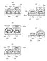
図1(A)〜(F)には、本発明の第一の実施形態のエッチング方法が適用される半導体装置の製造方法、例えばCMOS(Complementary Metal Oxide Semiconductor)トランジスタの製造方法が示されている。 1A to 1F show a method for manufacturing a semiconductor device to which the etching method according to the first embodiment of the present invention is applied, for example, a method for manufacturing a complementary metal oxide semiconductor (CMOS) transistor. .
図1(A)に示すように、シリコンからなる基板W上には、PMOSトランジスタ203及びNMOSトランジスタ204が形成される。基板Wは、素子分離領域によって、PMOS領域201とNMOS領域202とに分離されており、PMOS領域201にはPMOSトランジスタ203が、NMOS領域202にはNMOSトランジスタ204が設けられている。NMOS領域202にはポリシリコンからなるゲート電極205が形成される。ゲート電極205の側壁には、オフセットスペーサ206を介してサイドウォールスペーサ207が形成される。サイドウォールスペーサ207の表面には酸化シリコン膜208が形成される。ゲート電極205の両側にはソース・ドレイン領域209が形成される。ソース・ドレイン領域209に挟まれた領域がチャネル領域210になる。PMOS領域201にもゲート電極211が形成され、ゲート電極211の側壁にオフセットスペーサ212を介してサイドウォールスペーサ213が形成される。ゲート電極211の両側のシリコン基板Wにはソース・ドレイン領域が215形成され、ソース・ドレイン領域215に挟まれた領域がチャネル領域216になる。上記PMOSトランジスタ203及びNMOSトランジスタ204は、公知の成膜、エッチング、フォトリソグラフィ、イオン注入等の技術により形成される。ゲート電極205,211の表面及びソース・ドレイン領域209,215の表面には、NiSi,CoSi,又はTiSi等からなるシリサイド層が形成される。 As shown in FIG. 1A, a
上記のように形成されたNMOSトランジスタ204及びPMOSトランジスタ203のそれぞれに引張り又は圧縮方向の応力を与える応力誘起膜を作り分け、キャリアの移動度を最適化する技術がデユアルストレスライナー(Dual Stress Liner)技術である。NMOSトランジスタ204及びPMOSトランジスタ203のチャネル領域に応力を印加することにより、ドレイン電流が増大するので、トランジスタの性能を向上させることができる。 A technique for optimizing carrier mobility by creating a stress-inducing film that applies tensile or compressive stress to each of the
図1(B)に示すように、まず、基板Wの上にPMOSトランジスタ203及びNMOSトランジスタ204を覆うように引張り応力を与えるための窒化シリコン(SiN)膜220を形成する。窒化シリコン膜220は例えば化学的気相成長(CVD)により形成される。次に、窒化シリコン膜(SiN)220の上にハードマスクとなる酸化シリコン(SiO2)膜222を積層する。酸化シリコン膜222は例えば化学的気相成長(CVD)により形成される。次に、NMOSトランジスタ204の酸化シリコン膜222の上にフォトレジスト224を積層する。フォトレジスト224は公知のリソグラフィー技術を使用することにより形成することができる。As shown in FIG. 1B, first, a silicon nitride (SiN)
図1(C)に示すように、フォトレジスト224をマスクとして、PMOSトランジスタ203上の酸化シリコン膜222及び窒化シリコン膜220をエッチングする。図1(B)から図1(C)に至るエッチング工程に、本発明の第一の実施形態のエッチング方法が適用される。本発明の第一の実施形態のエッチング方法については後述する。 As shown in FIG. 1C, the
次に、図1(D)に示すように、基板W上のPMOSトランジスタ203及びパターニングされた窒化シリコン膜220a及び酸化シリコン膜222aを覆うように圧縮応力を与えるための窒化シリコン膜230を形成する。窒化シリコン膜230は例えば化学気相成長(CVD)により形成される。次に、PMOSトランジスタ203を覆い、かつNMOSトランジスタ204を覆わないマスクパターンをフォトレジスト231により形成する。 Next, as shown in FIG. 1D, a
図1(E)に示すように、フォトレジスト231をマスクとしてNMOSトランジスタ204上の窒化シリコン膜230をエッチングする。この窒化シリコン膜230のエッチングでは、酸化シリコンやフォトレジストに対する窒化シリコンの選択比の高いエッチングになる。この窒化シリコン膜230のエッチングに本発明のエッチング方法を適用してもよい。 As shown in FIG. 1E, the
次に、図1(F)に示すように、フォトレジスト231をマスクとしてNMOSトランジスタ204上のパターニングされた酸化シリコン膜222aをエッチングする。なお、この酸化シリコン膜222aのエッチングにも本発明のエッチング方法を適用してもよい。 Next, as shown in FIG. 1F, the patterned
アッシングによりフォトレジストを除去すると、PMOSトランジスタ203上に圧縮応力を与える窒化シリコン膜230aが形成され、NMOSトランジスタ204上に引張り応力を与える窒化シリコン膜220aが形成された状態になる。 When the photoresist is removed by ashing, a
図2は、本発明の第一の実施形態のエッチング方法の工程図を示す。この図2には、図1の(B)から(C)に至る工程が詳細に示されている。NMOSトランジスタ204上にフォトレジスト224が積層された基板W(図2(A)参照)は、RLSA(Radial Line Slot Antenna)エッチング装置に搬送される。RLSAエッチング装置の特徴は、低電子温度(低エネルギ)のプラズマを生成できる点にある。RLSAエッチング装置の構成、特徴については後述する。 FIG. 2 is a process chart of the etching method according to the first embodiment of the present invention. FIG. 2 shows the steps from (B) to (C) in FIG. 1 in detail. The substrate W (see FIG. 2A) in which the
このRLSAエッチング装置では、PMOSトランジスタ203上の絶縁膜としての酸化シリコン膜222及び窒化シリコン膜220をエッチングする。本発明の第一の実施形態のエッチング方法は、酸化シリコン膜222の大部分をエッチングする第一のエッチング(メインエッチング)工程、第一のエッチング工程で酸化シリコン膜222上に生成した堆積物を除去する堆積物除去工程としてのO2フラッシュ工程、第一のエッチング工程で残った薄い酸化シリコン膜222を除去する第二のエッチング(オーバーエッチング)工程、及び窒化シリコン膜220を除去する窒化シリコン膜エッチング工程を備える。いずれの工程もRLSAエッチング装置内で行われる。In this RLSA etching apparatus, the
第一のエッチング工程では、RLSAエッチング装置の処理容器に処理ガスを導入し、処理容器内に処理ガスのプラズマを発生させることによって、フォトレジスト224をマスクとしてPMOSトランジスタ203上の酸化シリコン膜222をエッチングする(図2(A)参照)。この第一のエッチング工程では、窒化シリコンに対する酸化シリコンの選択比を高めたエッチングが必要になり、かつフォトレジスト224を残すエッチングが必要になる。このため、堆積物(CFx等)を堆積しながらのエッチングが必要になる。そして、酸化シリコン膜222を途中まで厚さ方向にエッチングする。具体的には、残存する酸化シリコン膜222の厚さがエッチング前の厚さの5〜20%になるように、厚さを数値でいえば、残存する酸化シリコン膜222の厚さが10nm以下、望ましくは5nm以下になるように、酸化シリコン膜222をエッチングする。In the first etching step, a processing gas is introduced into the processing container of the RLSA etching apparatus, and plasma of the processing gas is generated in the processing container, so that the
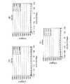
表1は第一のエッチング(メインエッチング)工程の処理条件の一例を示す。 Table 1 shows an example of processing conditions for the first etching (main etching) step.

処理ガスの種類は、エッチングすべき材料によって決定され、Ar,He,Ne,Kr及びXeの少なくも一つを含むプラズマ励起用ガスと、エッチングガスとを混合したガスが用いられる。エッチングガスには、CH2F2,CHF3,及びCH3Fの群から選ばれる少なくとも一つ、並びにO2,CO,CN,及びN2の群から選ばれる少なくとも一つを混合したガスが用いられる。酸化シリコン膜をエッチングするこの例では、Ar、CHF3、O2の混合ガスが使用される。エッチングガスのうち、CHF系ガスを用いると基板Wに堆積物が生じる。O2,CO,CN,又はN2などは堆積物中の炭素成分の量を調整するために使用される。The type of processing gas is determined by the material to be etched, and a gas obtained by mixing a plasma excitation gas containing at least one of Ar, He, Ne, Kr, and Xe and an etching gas is used. The etching gas includes a gas in which at least one selected from the group of CH2 F2 , CHF3 , and CH3 F and at least one selected from the group of O2 , CO, CN, and N2 are mixed. Used. In this example of etching the silicon oxide film, a mixed gas of Ar, CHF3 , and O2 is used. Among the etching gases, deposits are generated on the substrate W when a CHF-based gas is used. O2 , CO, CN, N2 or the like is used to adjust the amount of carbon components in the deposit.
図2(B)に示すように、第一のエッチング(メインエッチング)工程が終了すると、窒化シリコン膜220の上には薄い酸化シリコン膜222が残り、酸化シリコン膜222の上にはCF系の堆積物225が生ずる。堆積物225は少なくともカーボン及びフッ素を含み、第一のエッチング工程の間に酸化シリコン膜222の上に堆積する。堆積物225を除去するために、堆積物225を除去するO2フラッシュ工程が行われる。ここで、O2フラッシュとは、低エネルギの酸素プラズマを被処理膜に晒すことをいう。これにより、堆積物を除去することができる。As shown in FIG. 2B, when the first etching (main etching) step is completed, a thin
堆積物225を除去するO2フラッシュ工程では、RLSAエッチング装置内で酸素プラズマを発生させる(O2flash)。すなわち、RLSAエッチング装置の処理容器に酸素ガスを導入し、処理容器内に酸素プラズマを発生させる。堆積物225を酸素プラズマ中に晒すと、プラズマ中の酸素ラジカルと堆積物225が反応し、二酸化炭素と水になり、蒸発、そして排気除去される。窒化シリコン膜220の上には薄い酸化シリコン膜222が残っているので、O2フラッシュを経ても窒化シリコン膜220の表層は酸化されることがなく、酸化シリコンに変質することがない。もちろん、酸化シリコン膜222はもともと酸化されているので、O2フラッシュしてもほとんど変化がない。In the O2 flash process for removing the
ここで、O2フラッシュをしないと仮定すると、酸化シリコン膜222のエッチングを終了したとき、窒化シリコン膜220の表面にはCF系の堆積物が堆積する。CF系の堆積物が堆積すると、CF系の堆積物がエッチングマスクになって、窒化シリコン膜220のエッチングが局所的に進まなくなる。CF系の堆積物を除去することにより、これを防止することができる。しかも、O2フラッシュするとき、窒化シリコン膜220の表面には酸化シリコン膜222が薄く残存する。このため、窒化シリコン膜220の表層が酸素プラズマによって酸化してしまうのを防止できる。Here, assuming that the O2 flash is not performed, CF-based deposits are deposited on the surface of the
堆積物は、表2に示す条件のもと酸素プラズマ処理される。 The deposit is subjected to oxygen plasma treatment under the conditions shown in Table 2.
NMOSトランジスタ204上には、フォトレジスト224が形成されている(図2(B)参照)。フォトレジスト224もカーボン及びフッ素を含むので、O2フラッシュを強力に行うと、フォトレジスト224がプラズマ中の酸素ラジカルと結合し、二酸化炭素と水になり、蒸発・除去される。フォトレジスト224が除去されるのを防止するために、電子温度の低い酸素プラズマにする必要がある。しかも、薄く残存する酸化シリコン膜222の下には、窒化シリコン膜220が形成されている。酸素プラズマによって、薄い酸化シリコン膜222を介して窒化シリコン膜220が酸化されるのを防止するためにも、酸素プラズマの電子温度を低くする必要がある。RLSAのエッチング装置を使用し、処理容器内の圧力を100mTorr以上の高圧にし、マイクロ波パワーを3000W以下に低くすれば、電子温度の低い、すなわちエネルギの低い酸素プラズマを生成することができる。酸素プラズマの処理時間は、フォトレジスト224や下地の窒化シリコン膜220に悪影響を与えない短いように10秒程度に設定される。A
図2(C)に示すように、O2フラッシュにより酸化シリコン膜222の表面の堆積物225が除去される。窒化シリコン膜220の上には厚さが100nm以下にまで減じられた薄い酸化シリコン膜222が形成されている。薄い酸化シリコン膜222の厚さ方向の全体を除去するために、窒化シリコンに対する酸化シリコンの選択比を高めた第二のエッチング(オーバーエッチング)工程が行われる。第二のエッチング工程も、堆積物(CFx等)を堆積しながらのエッチングになる。As shown in FIG. 2C, the
表3は第二のエッチング工程の処理条件の一例を示す。 Table 3 shows an example of processing conditions for the second etching step.
処理ガスの種類は、第一のエッチング工程と同一であるが、RFバイアスを第一のエッチング工程よりも僅かに大きくし、処理時間を60秒と短くしている。 The type of the processing gas is the same as that in the first etching process, but the RF bias is slightly larger than that in the first etching process, and the processing time is shortened to 60 seconds.
図2(D)に示すように、第二のエッチング(オーバーエッチング)工程によって、酸化シリコン膜222が除去される。第二のエッチング工程においても堆積物は生成する。しかし、酸化シリコン膜222は当初の10%以下程度と薄くなっているので、第2のエッチング中に生成する堆積物の量は少ない。堆積物の量がエッチング量に比例すると仮定すると、堆積物の量も10%程度になる。堆積物の量が少なくなると、堆積物を除去しなくても窒化シリコン膜220の十分に均一なエッチングが可能になる。 As shown in FIG. 2D, the
酸化シリコン膜222のエッチングが終了したら、アッシングによりNMOSトランジスタ204上のフォトレジスト224を除去する。このアッシングにおいては、窒化シリコンや酸化シリコンに対するフォトレジストのエッチング選択比を高くする必要がある。 When the etching of the
PMOSトランジスタ203上の窒化シリコン膜220は、窒化シリコン膜エッチング工程により厚さ方向の全体が除去される。窒化シリコン膜エッチング工程では、RLSAエッチング装置の処理容器に処理ガスを導入し、窒化シリコン膜220をエッチングする。窒化シリコン膜220の表面は酸化されておらず、しかも表面に堆積する堆積物の量も少ないので、O2フラッシュを行わなくても窒化シリコン膜220のエッチングが可能になる。なお、窒化シリコン膜220の下層には、酸化シリコン膜214(PMOSトランジスタ203のスペーサ)が形成されているので、酸化シリコンに対する窒化シリコンの選択比を高めたエッチングが必要になる。The entire
表4は窒化シリコン膜エッチング工程の処理条件の一例を示す。 Table 4 shows an example of processing conditions of the silicon nitride film etching process.
処理ガスの種類は、エッチングすべき材料によって決定され、Ar,He,Ne,Kr及びXeの少なくも一つを含むプラズマ励起用ガスと、エッチングガスとを混合したガスが用いられる。エッチングガスには、CH2F2,CHF3,及びCH3Fの群から選ばれる少なくとも一つ、並びにO2,CO,CN,及びN2の群から選ばれる少なくとも一つを混合したガスが用いられる。窒化シリコン膜220をエッチングするこの例では、Ar,CH2F2,O2の混合ガスが使用される。窒化シリコン膜のエッチング工程において、圧力を低い→高い、の2段階にしても良い。The type of processing gas is determined by the material to be etched, and a gas obtained by mixing a plasma excitation gas containing at least one of Ar, He, Ne, Kr, and Xe and an etching gas is used. The etching gas includes a gas in which at least one selected from the group of CH2 F2 , CHF3 , and CH3 F and at least one selected from the group of O2 , CO, CN, and N2 are mixed. Used. In this example of etching the
基板Wに照射されるイオンエネルギは、プラズマのエネルギと基板Wに印加されるバイアス電圧の和と相関関係がある。RFバイアスを0にすることにより、プラズマのエネルギだけでエッチングできるようになる。さらに、500mTの高圧でエッチングすることにより、プラズマの電子温度、すなわちプラズマのエネルギを低下させることができる。EFバイアスとプラズマのエネルギとの和を小さくすることができるので、下地となるシリコン酸化膜214やシリコン基板Wにダメージ(リセス)が入るのを防止できる。 The ion energy applied to the substrate W has a correlation with the sum of the plasma energy and the bias voltage applied to the substrate W. By setting the RF bias to 0, etching can be performed only with plasma energy. Further, by etching at a high pressure of 500 mT, the plasma electron temperature, that is, the plasma energy can be lowered. Since the sum of the EF bias and the plasma energy can be reduced, damage (recess) can be prevented from entering the underlying
PMOSトランジスタ203上の酸化シリコン膜222及び窒化シリコン膜220のエッチングが終了したら、図2(E)に示す状態(図1(C)と同じ状態)になる。 When etching of the
図3は、異なる圧力の下でのフォトレジストのエッチングレートの実験結果を示す。この実験では、O2フラッシュは、各圧力の下、10秒間、3000Wのマイクロ波パワーをKrFレジストに供給することによって行われた。図3(A)〜(D)において横軸の単位はmmであり、縦軸の単位はÅである。基板W上にX軸、Y軸、V軸、W軸をとり、四方向のエッチングレートを測定している。横軸の0は基板Wの中心を表す。FIG. 3 shows the experimental results of photoresist etch rate under different pressures. In this experiment, an O2 flush was performed by supplying 3000 W of microwave power to the KrF resist for 10 seconds under each pressure. 3A to 3D, the unit of the horizontal axis is mm, and the unit of the vertical axis is Å. The X-axis, Y-axis, V-axis, and W-axis are taken on the substrate W, and the etching rates in four directions are measured. 0 on the horizontal axis represents the center of the substrate W.
図3(A)によれば、圧力が20mTのとき、エッチングレートは10秒間で114.0nmであり、高い値を保つ。図3(B)によれば、圧力が60mTのとき、エッチングレートは10秒間で87.7nmであり、まだ高い値を保つ。圧力が60mTのときのフォトレジストのエッチングレートはまだ高い値なので、エッチングレートをさらに低くするために、O2フラッシュを60mTよりも高い圧力で行う必要がある。According to FIG. 3 (A), when the pressure is 20 mT, the etching rate is 114.0 nm in 10 seconds, and maintains a high value. According to FIG. 3B, when the pressure is 60 mT, the etching rate is 87.7 nm in 10 seconds, and still maintains a high value. Since the etching rate of the photoresist when the pressure is 60 mT is still high, it is necessary to perform O2 flash at a pressure higher than 60 mT in order to further reduce the etching rate.
図3(C)によれば、圧力が100mTのとき、エッチングレートは10秒間で39.7nmであり、低い値になる。エッチングレートを39.7nm/10secより低くするため、O2フラッシュは100mT以上で行われるのが望ましい。図3(D)によれば、200mTのとき、エッチングレートは10秒間で20.5nmであり、より低い値になる。100mTのときよりもエッチングレートを低くすることができるので、O2フラッシュは200mTで行われてもよい。According to FIG. 3C, when the pressure is 100 mT, the etching rate is 39.7 nm in 10 seconds, which is a low value. In order to make the etching rate lower than 39.7 nm / 10 sec, the O2 flash is desirably performed at 100 mT or more. According to FIG. 3D, at 200 mT, the etching rate is 20.5 nm for 10 seconds, which is a lower value. Since the etching rate can be made lower than that at 100 mT, the O2 flush may be performed at 200 mT.
図4は、マイクロ波パワーを変化させたときのフォトレジストのエッチングレートの実験結果を示す。O2フラッシュは、100mTの圧力の下、5秒間、1500W、2000W、3000Wの各マイクロ波パワーをKrFレジストに供給することによって行われた。FIG. 4 shows the experimental result of the etching rate of the photoresist when the microwave power is changed. The O2 flash was performed by supplying each microwave power of 1500 W, 2000 W, 3000 W to the KrF resist for 5 seconds under a pressure of 100 mT.
図4(A)によれば、1500Wのとき、エッチングレートは2秒間で9.3nmであり、低い値になる。図4(B)によれば、2000Wのとき、エッチングレートは2秒間で12.6nmであり、少し高くなるもののまだ低い値を保つ。図4(C)によれば、3000Wのとき、エッチングレートは2秒間で24.2nmであり、2000Wのときの倍の高い値になる。エッチングレートを低くするために、マイクロ波パワーは2000Wに設定されるが望ましい。マイクロ波パワーが1500Wのときはよりエッチングレートを低くすることができるので、1500Wに設定されてもよい。 According to FIG. 4A, at 1500 W, the etching rate is 9.3 nm for 2 seconds, which is a low value. According to FIG. 4 (B), at 2000 W, the etching rate is 12.6 nm in 2 seconds, which is slightly higher, but still keeps a low value. According to FIG. 4C, at 3000 W, the etching rate is 24.2 nm for 2 seconds, which is twice as high as 2000 W. In order to lower the etching rate, the microwave power is preferably set to 2000W. Since the etching rate can be lowered when the microwave power is 1500 W, it may be set to 1500 W.
図5(A)〜(F)には、本発明の第二の実施形態のエッチング方法が適用される半導体装置の製造方法、例えばMOSFETの製造方法が示されている。図5(A)に示すように、シリコン基板Wの表面には、ポリシリコンからなるゲート電極301がゲート絶縁膜302、例えば酸化シリコン膜を介して形成される。次に、図5(B)に示すように、シリコン基板Wの表面304及びゲート電極301の表面に酸化シリコン(SiO2)膜303が化学的気相成長(CVD)により形成される。5A to 5F show a semiconductor device manufacturing method to which the etching method of the second embodiment of the present invention is applied, for example, a MOSFET manufacturing method. As shown in FIG. 5A, a
次に、シリコン基板WはRLSAエッチング装置に搬送される。RLSAエッチング装置では、ゲート電極301の側壁にオフセットスペーサ303a(図1(E)参照)を形成するために、堆積された酸化シリコン膜303をエッチングする。 Next, the silicon substrate W is transferred to the RLSA etching apparatus. In the RLSA etching apparatus, the deposited
図5(B)から図5(E)に至る過程に、本発明の第二の実施形態のエッチング方法が適用される。第二の実施形態のエッチング方法は、酸化シリコン膜303の大部分をエッチングする第一のエッチング(メインエッチング)工程、第一のエッチング工程で生成した堆積物を除去するO2フラッシュ工程、第一のエッチング工程で残った薄い酸化シリコン膜303を除去する第二のエッチング(オーバーエッチング)工程を備える。いずれの工程もRLSAエッチング装置内で行われる。In the process from FIG. 5B to FIG. 5E, the etching method of the second embodiment of the present invention is applied. The etching method of the second embodiment includes a first etching (main etching) step that etches most of the
第一のエッチング工程では、RLSAエッチング装置の処理容器に処理ガスを導入し、処理容器内にプラズマを発生させることによって、酸化シリコン膜303をエッチングする。この第一のエッチング工程では、シリコンやポリシリコンに対する酸化シリコンの選択比を高めたエッチングが必要になり、堆積物(CFx)を生成しながら酸化シリコン膜303が当初の膜厚の例えば5〜20%になるように厚さ方向にエッチングする。In the first etching step, the
図5(C)に示すように、第一のエッチング工程が終了すると、シリコン基板Wの上には薄い酸化シリコン膜303が残った状態になり、酸化シリコン膜303の上には堆積物305が付着する。堆積物305は少なくともカーボンを含む。堆積物305を除去するために、O2フラッシュ工程が行われる。As shown in FIG. 5C, when the first etching process is completed, a thin
堆積物305を除去するO2フラッシュ工程では、RLSAエッチング装置内で酸素プラズマをフラッシュさせる(O2flash)。堆積物305を酸素プラズマ中に置くと、プラズマ中の酸素ラジカルと堆積物が結合し、二酸化炭素と水になり、蒸発・除去される。シリコン基板Wの上には薄い酸化シリコン膜303が残っているので、O2フラッシュしてもシリコン基板Wは酸化されることがなく、シリコン基板Wにダメージ(リセス)が入るのを防止できる。In the O2 flash process for removing the
O2フラッシュにより酸化シリコン膜303の表面の堆積物が除去される(図5(D)参照)。シリコン基板Wの上には厚さが10%程度まで減じられた薄い酸化シリコン膜303が形成されている。薄い酸化シリコン膜303の厚さ方向の全体を除去するために、シリコン基板Wやポリシリコンに対する酸化シリコンの選択比を高めた第二のエッチング工程が行われる。第二のエッチング工程も、堆積物(CFx等)を生じながらのエッチングになるが、酸化シリコン膜303は薄いので、堆積物の量も少ない。なお、必要に応じて再度のO2フラッシュを行ってもよい。第二のエッチング工程が終了すると、シリコン基板Wの表面が露出した状態になる(図5(E)参照)。Deposits on the surface of the
次に、図5(F)に示すように、シリコン基板Wにエクステンション領域306を形成するために、シリコン基板Wに燐イオンを注入する。次に、サイドウォールスペーサを形成するために、図5(G)に示すように、シリコン基板Wの表面304及びゲート電極301を覆うように窒化シリコン膜307が形成される。窒化シリコン膜307は化学的気相成長(CVD)により形成される。 Next, as shown in FIG. 5F, phosphorus ions are implanted into the silicon substrate W in order to form
次にRLSAエッチング装置において、ゲート電極301の側壁にサイドウォールスペーサ307a(図5(J)参照)を形成するため、窒化シリコン膜307がエッチングされる。 Next, in the RLSA etching apparatus, the
図5(G)から図5(J)に至るエッチング過程に、本発明の第三の実施形態のエッチング方法が適用される。第三の実施形態のエッチング方法は、窒化シリコン膜307の大部分をエッチングする第一のエッチング(メインエッチング)工程、第一のエッチング工程で生成した堆積物を除去するO2フラッシュ工程、第一のエッチング工程で残った薄い窒化シリコン膜307を除去する第二のエッチング(オーバーエッチング)工程を備える。いずれの工程もRLSAエッチング装置内で行われる。The etching method of the third embodiment of the present invention is applied to the etching process from FIG. 5 (G) to FIG. 5 (J). The etching method of the third embodiment includes a first etching (main etching) step for etching most of the
第一のエッチング工程では、RLSAエッチング装置の処理容器に処理ガスを導入し、処理容器内にプラズマを発生させることによって、窒化シリコン膜307をエッチングする。この第一のエッチング工程では、シリコンやポリシリコンに対する窒化シリコンの選択比を高めたエッチングが必要になり、堆積物(CFx)を堆積しながら窒化シリコン膜307が当初の膜厚の例えば5〜20%になるようにエッチングする。In the first etching step, the
図5(H)に示すように、第一のエッチング工程が終了すると、シリコン基板Wの上には薄い窒化シリコン膜307が残った状態になり、窒化シリコン膜307の上には堆積物308が堆積する。堆積物308は少なくともカーボン及びフッ素を含む。堆積物308を除去するために、O2フラッシュ工程が行われる。As shown in FIG. 5H, when the first etching process is completed, a thin
堆積物308を除去するO2フラッシュ工程では、RLSAエッチング装置内で酸素プラズマをフラッシュさせる(O2flash)。堆積物308を酸素プラズマ中に置くと、プラズマ中の酸素ラジカルと堆積物308が結合し、二酸化炭素と水になり、蒸発・除去される。シリコン基板Wの上には薄い窒化シリコン膜307が残っているので、O2フラッシュしてもシリコン基板Wは酸化されることがなく、シリコン基板Wにダメージ(リセス)が入るのを防止できる。In the O2 flash process for removing the deposit 308, oxygen plasma is flashed in the RLSA etching apparatus (O2 flash). When the deposit 308 is placed in oxygen plasma, oxygen radicals in the plasma and the deposit 308 are combined to form carbon dioxide and water, which are evaporated and removed. Since the thin
O2フラッシュにより窒化シリコン膜307の表面の堆積物308を除去したら、シリコン基板Wの上には厚さが10%程度まで減じられた薄い窒化シリコン膜307が形成されている状態になる(図5(I)参照)。薄い窒化シリコン膜307の厚さ方向の全体を除去するために、シリコン基板Wやポリシリコンに対する窒化シリコンの選択比を高めた第二のエッチング工程が行われる。第二のエッチング工程も、堆積物(CFx等)で側壁を保護しながらのエッチングを行なうが、窒化シリコン膜307は薄いので、堆積物の量も少ない。なお、堆積物を除去する必要があれば、再度O2フラッシュを行えばよい。When the deposit 308 on the surface of the
次に、シリコン基板Wにソース/ドレイン領域を形成するためのヒ素イオンが注入される(図5(J)参照)。サイドウォールスペーサ307aを形成することで、エクステンション領域の外側に高濃度のソース/ドレイン領域310を形成することができる。 Next, arsenic ions for forming source / drain regions are implanted into the silicon substrate W (see FIG. 5J). By forming the
この半導体装置の製造方法では、オフセットスペーサ及びサイドウォールスペーサの両方が形成されているが、オフセットスペーサが形成されることなく、サイドウォールスペーサのみが形成されてもよい。 In this method of manufacturing a semiconductor device, both the offset spacer and the side wall spacer are formed. However, only the side wall spacer may be formed without forming the offset spacer.
上記第一ないし第三の実施形態のエッチング方法では、RLSAエッチング装置が使用されているが、プラズマを生成することができる他のプラズマ処理装置も使用することができる。RLSAエッチング装置の構成は以下の通りである。 In the etching methods of the first to third embodiments, the RLSA etching apparatus is used, but other plasma processing apparatuses capable of generating plasma can also be used. The configuration of the RLSA etching apparatus is as follows.
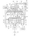
図6は、RLSAエッチング装置の概略断面図を示す。RLSAエッチング装置は、プラズマ源としてマイクロ波励起プラズマを利用する。マイクロ波励起プラズマを利用すると、エッチング処理を行う領域において低電子温度、高密度のプラズマを生成することができる。 FIG. 6 shows a schematic cross-sectional view of the RLSA etching apparatus. The RLSA etching apparatus uses microwave-excited plasma as a plasma source. When microwave-excited plasma is used, plasma with a low electron temperature and high density can be generated in the region where the etching process is performed.
RLSAによって生成されたマイクロ波プラズマの特徴は、誘電体窓52直下(プラズマ励起領域と呼ばれる)で生成された数eVのプラズマが拡散し、基板W直上(拡散プラズマ領域)では約1〜2eV程度の低い電子温度のプラズマとなることにある。すなわち、平行平板等のプラズマとは異なり、プラズマの電子温度の分布が誘電体窓52からの距離の関数として明確に生ずることに特徴がある。より詳細には、図7に示したとおり、誘電体窓52直下での数eV〜10eVの電子温度が、基板W上では約1〜2eV程度に減衰する。基板Wの処理はプラズマの電子温度の低い領域(拡散プラズマ領域)で行なわれるため、基板Wにリセス等の大きなダメージを与えることがない。 The characteristics of the microwave plasma generated by RLSA is that several eV of plasma generated just below the dielectric window 52 (called plasma excitation region) diffuses, and about 1-2 eV just above the substrate W (diffusion plasma region). The result is a low electron temperature plasma. That is, unlike plasma such as a parallel plate, the electron temperature distribution of the plasma is clearly generated as a function of the distance from the
RLSAエッチング装置は、アルミニウム合金、ステンレス合金等からなる筒状の処理容器10を備える。処理容器10は接地されている。 The RLSA etching apparatus includes a
初めに、RLSAエッチング装置の処理容器10にマイクロ波励起プラズマを発生させることに直接的に貢献しない構成要素や部材について説明する。 First, components and members that do not directly contribute to generating microwave-excited plasma in the
処理容器10の底部の中央には、基板Wが載せられる載置台としてのサセプタ12が設けられる。サセプタ12は処理容器10の底部から上方に伸びる円筒状の支持部14により保持される。サセプタ12は、例えばアルミナや窒化アルミナ等の絶縁材料からなり、円盤状に形成される。サセプタ12は、高周波が印加される下部電極として機能する。 A
処理容器10の内側面と、円筒状の支持部14を囲み、処理容器10の底部から上方に伸びる円筒状の壁部16との間には、円環形状の排気経路18が設けられる。排気経路18の上部には円環形状のバッフルプレート20が配置され、排気経路18の下部には排気口22が設けられる。サセプタ12の上の基板Wに関して対称に分布する均一なガスの流れを得るために、円環形状の排気経路18には周方向に等しい角度間隔を空けて多数の排気口22が設けられる。各排気口22は排気パイプ24を介して排気装置26に接続される。排気装置26は、処理容器10内を真空にし、所望の圧力に減圧する排気手段としてのターボ分子真空ポンプ(TMP)等の真空ポンプを備える。ゲートバルブ28は、基板Wが処置容器から搬出入される搬送口を開閉する。 An
サセプタ12は、整合器32、電力供給ロッド34を介してサセプタ12にRFバイアス電圧を印加する高周波電源30に電気的に接続される。高周波電源30は、所定の電力レベルにおいて、例えば13.56MHzの比較的低い周波数の高周波を出力する。このような低い周波数は、サセプタ12上の基板Wに引き込むイオンのエネルギを調整するのに適している。整合器32は、高周波電源30の出力インピーダンスを、電極(サセプタ12)、処理容器10内に生成されたプラズマ、及び処理容器10を含む負荷のインピーダンスに整合するための整合要素を備える。整合要素は、自己バイアスを発生させるためのブロックコンデンサ(blocking condenser)を有する。 The
サセプタ12の上面には、静電チャック36が設けられる。静電チャック36は、サセプタ12上に基板Wを静電力によって保持する。静電チャック36は、導体膜から形成される電極36aと、電極36aを上下に挟む一対の絶縁膜36b,36cと、を備える。直流電源40は、スイッチ42を介して電極36aに電気的に接続される。直流電源40から静電チャック36に印加される直流電圧は、静電チャック36上に基板Wを保持するためのクーロン力を生じさせる。静電チャック36の外周には、基板Wを囲むフォーカスリング38が設けられる。 An
サセプタ12の内部には、冷却媒体経路44が設けられる。冷却媒体経路44は周方向に伸び、円環形状に形成される。所定温度の冷却媒体又は冷却水が、導管48及び冷却媒体経路44を循環するようにチラーユニット(図示せず)から導管48を介して冷却媒体経路44に供給される。冷却媒体の温度を調整することにより、静電チャック36上の基板Wの温度を調整することができる。さらに、Heガス等の熱伝導ガスが基板Wと静電チャックとの間に、ガス供給部(図示せず)から供給パイプ50を介して供給される。 A cooling
次に、RLSAエッチング装置の処理容器10にマイクロ波プラズマを発生させるのに貢献する要素や部材を説明する。 Next, elements and members that contribute to generating microwave plasma in the
平面アンテナ55は、石英、セラミックス、アルミナ(Al2O3)、又は窒化アルミニウム(AlN)などの誘電体からなる円盤状の誘電体窓52と、丸い板状のスロットアンテナ54と、を備える。誘電体窓52は、処理容器10の内部を密封するように処理容器10に取り付けられ、サセプタ12に対向する処理容器10の天井部として機能する。スロットアンテナ54は誘電体窓52の上面の上に配置され、同心円状に分布する多数のスロットを有する。スロットアンテナ54は、石英等の誘電体からなる波長圧縮板としての誘電体板56を介して電磁的にマイクロ波導入路58に連結される。The
マイクロ波導入路58は、導波路62と、導波路/同軸管変換器64と、同軸管66と、を有し、マイクロ波発生器60から出力されたマイクロ波をスロットアンテナ54に伝送する。導波路62は、例えば矩形状のパイプから形成され、マイクロ波発生器60から変換器64にTEモードでマイクロ波を伝送する。 The
変換器64は、導波路62を同軸管66に連結させ、導波路62内のTEモードのマイクロ波を同軸管66内のTEMモードのマイクロ波に変換する。変換器64は、下方に向かって尖った円錐形状に形成され、その上部が導波路62に結合され、その下部が同軸管66の内側導体68に結合される。 The
同軸管66は、変換器64から処理容器10の上部中央に向かって垂直下方に伸び、スロットアンテナ54に連結される。同軸管66は、外側導体70と、内側導体68と、を有する。外側導体70は、その上端部が導波路62に結合され、垂直下方に伸びる下端部が誘電体板56に結合される。内側導体68はその上端部が変換器64に接続され、その下端部がスロットアンテナ54に到達まで垂直下方に伸びる。マイクロ波は外側導体70と内側導体68との間をTEMモードで伝播する。 The
マイクロ波発生器から出力されたマイクロ波は、導波路62、変換器64、同軸管66を含むマイクロ波導入路58を伝送され、誘電体板56を通過した後、スロットアンテナ54に供給される。マイクロ波は誘電体板56を半径方向に拡散し、スロットアンテナ54のスロットを介して処理容器10内に放射される。これにより、誘電体窓52の直下のガスがイオン化され、処理容器10内にプラズマが発生する。 The microwave output from the microwave generator is transmitted through the
誘電体板56の上面にはアンテナ背面プレート72が設けられる。アンテナ背面プレート72は例えばアルミニウムからなる。アンテナ背面プレート72には、チラーユニット(図示せず)に接続される流路74が形成される。所定温度の冷却媒体又は冷却水は流路74及びパイプ76,78内を循環する。アンテナ背面プレート72は誘電体板56に発生する熱を吸収する冷却ジャケットとして機能し、熱を外部に排出する。 An antenna back
この実施形態では、ガス導入路80は同軸管66の内側導体68を貫通するように設けられる。第一のガス導入パイプ84は、その一端がガス導入路80の上端開口部80aに接続され、その他端が処理ガス供給源82に接続される。誘電体窓52の中央には、処理容器10に向かって開口するガス噴射口86が形成される。上記の構成を備える第一のガス導入部88において、処理ガス供給源82からの処理ガスは、第一のガス導入パイプ84、及び内側導体68内のガス導入路80を流れ、ガス噴射口86から下方に位置するサセプタ12に向かって噴射される。処理ガスは排気装置26によってサセプタ12を囲む円環状の排気経路18に引かれているので、噴射された処理ガスは処理容器10内を半径方向外側に拡散する。第一のガス導入パイプ84の途中には流量調整器90(MFC)と、オンオフを行うバルブ92が設けられる。 In this embodiment, the
この実施形態では、第一のガス導入部88に加えて、処理容器10に処理ガスを供給するための第二のガス導入部94が設けられる。第二のガス導入部94は、処理容器10内に配置されるガスリング91と、ガスリング91に接続されるガス供給管100と、を備える。ガスリング91は中空のリング形状に形成され、その内周側の側面には周方向に等しい角度間隔を空けて多数の側面噴射口92を有する。多数の側面噴射口92は処理容器10のプラズマ領域内で開口する。ガス供給管100は、ガスリング91及び処理ガス供給源82に接続される。ガス供給管100の途中には、流量調整器102(MFC)、及びオンオフを行う104バルブが設けられる。上記第一のガス導入部88及び第二のガス導入部94が処理ガス導入手段を構成する。 In this embodiment, in addition to the first
第二のガス導入部94において、処理ガス供給源82からの処理ガスはガス供給管100を介してガスリング91に導入される。処理ガスが充満するガスリング91の内部圧力は、周方向において均一になり、多数の側面噴射口92から処理容器10内のプラズマ領域に均一に水平方向に処理ガスが噴射される。ガスリング91からプラズマの電子温度の低い領域(プラズマ拡散領域)へ処理ガスが供給されるので、処理ガスの解離の状態を制御することができる。 In the second
図8は、スロットアンテナ54のスロットパターンの一例を示す。スロットアンテナ54は、同心円状に配列する多数のスロット54b,54cを有する。詳しくは、長手方向が直交する二種類のスロットが同心円状に交互に配列される。同心円の半径方向の間隔は、スロットアンテナ54を半径方向に伝播するマイクロ波の波長に基づいて定められる。このスロットパターンによれば、マイクロ波は互いに直交する二つの偏向成分を備える平面波に変換され、平面波がスロットアンテナ54から放射される。このように構成されたスロットアンテナ54は、アンテナの全領域から処理容器10内に均一にマイクロ波を放射するのに効果的であり、アンテナの下方に均一な安定したプラズマを生成するのに適している。 FIG. 8 shows an example of a slot pattern of the
排気装置26、高周波電源30、直流電源40、スイッチ42、マイクロ波発生器60、処理ガス供給源82、チラーユニット(図示せず)、熱伝導ガス供給部(図示せず)等の個々の作動、及び全体の作動は、制御部(図示せず)によって制御される。制御部は、例えばマイクロコンピュータ等から構成される。 Individual operations of the
なお、本発明は、上記教示を考慮して様々に修正・変化可能である。具体的な実施態様については、本発明の範囲から逸脱しない範囲で種々の変形・変更を加えることが可能である。 The present invention can be variously modified and changed in consideration of the above teaching. About a concrete embodiment, it is possible to add various modification and change in the range which does not deviate from the range of the present invention.
10…処理容器
22…排気口
12…サセプタ(載置台)
54…スロットアンテナ
60…マイクロ波発生器
58…マイクロ波導入路58
82…処理ガス供給源
88…第一のガス導入部
94…第二のガス導入部
203…PMOSトランジスタ
204…NMOSトランジスタ
220…窒化シリコン膜
222…酸化シリコン膜
225…堆積物
301…ゲート電極
303…酸化シリコン膜
303a…オフセットスペーサ
305,308…堆積物
307…窒化シリコン膜
307…窒化シリコン膜
307a…サイドウォールスペーサ
308…堆積物
W…シリコン基板(基板)
10 ... Processing
54 ...
82 ... Processing
Claims (13)
Translated fromJapanese前記絶縁膜をプラズマ化させた炭素、フッ素、酸素及び水素を含む第一の処理ガスに晒し、前記絶縁膜を厚さ方向に途中までエッチングすると共に、前記絶縁膜上に堆積物を生成する第一のエッチング工程と、
前記第一のエッチング工程の終了後、前記堆積物を酸素プラズマに晒し、前記酸素プラズマにより前記堆積物を除去する堆積物除去工程と、
前記残存する絶縁膜をプラズマ化させた炭素、フッ素、酸素及び水素を含む第二の処理ガスに晒し、前記残存する絶縁膜をエッチングする第二のエッチング工程と、を備えるエッチング方法。A method of etching an insulating film formedon a base film of a substrate,
The insulating film is exposed to afirst processing gascontaining carbon, fluorine, oxygen, and hydrogen that has been turned into plasma,and the insulating film is etched partway along the thickness direction,and deposits are generated on the insulating film . An etching process;
A deposit removal step of exposing thedeposit to oxygen plasmaafter the first etching step and removing the depositby the oxygen plasma ;
A second etching step in which the remaining insulating film is exposed to asecond processing gascontaining carbon, fluorine, oxygen, and hydrogen that has been turned into plasma,and the remaining insulating film is etched.
前記第一及び前記第二のエッチング工程では、前記酸化シリコン膜をエッチングすることを特徴とする請求項1ないし5のいずれかに記載のエッチング方法。The insulating film is a silicon oxide film laminated on a silicon nitride film,
Wherein in the first and the second etching step, an etching method according toany one of claims 1to 5, wherein etching the silicon oxide film.
前記絶縁膜は、前記シリコン基板の上に形成される酸化シリコン膜であり、
前記エッチング方法は、前記ゲート電極の側壁にオフセットスペーサ又はサイドウォールスペーサを形成するためのエッチング方法であることを特徴とする請求項1ないし8のいずれか1項に記載のエッチング方法。The substrate is a silicon substrate;
The insulating layer,Riacid silicon Makudeathat will be formed on the siliconsubstrate,
9. The etching method according to claim 1, wherein the etching method is an etching method for forming an offset spacer or a side wall spacer on a side wall of the gate electrode .
前記処理容器の内部に設けられ、基板を載置する載置台と、
前記処理容器の前記誘電体窓の上面に設けられ、前記処理容器の処理空間に多数のスロットを介してマイクロ波を導入するスロットアンテナと、
所定の周波数のマイクロ波を発生するマイクロ波発生器と、
前記マイクロ波発生器が発生するマイクロ波を前記スロットアンテナに導くマイクロ波導入路と、
処理ガス供給源から供給される処理ガスを前記処理容器に導入する処理ガス導入手段と、
前記処理容器内に導入された処理ガスを、前記載置台に載置された基板の上面より下方の排気口から排気する排気手段と、
請求項1ないし11のいずれかに記載のエッチング方法を実行する制御部と、を備えることを特徴とするエッチング装置。A processing vessel that has a dielectric window that transmits microwaves on the ceiling, and that can keep the inside airtight,
A mounting table provided inside the processing container and for mounting a substrate;
A slot antenna that is provided on an upper surface of the dielectric window of the processing container and introduces microwaves into the processing space of the processing container through a number of slots;
A microwave generator for generating microwaves of a predetermined frequency;
A microwave introduction path for guiding the microwave generated by the microwave generator to the slot antenna;
A processing gas introduction means for introducing a processing gas supplied from a processing gas supply source into the processing container;
Exhaust means for exhausting the processing gas introduced into the processing container from an exhaust port below the upper surface of the substrate placed on the mounting table;
An etching apparatus comprising:a control unit that executes the etching method according to claim 1 .
素子、及び素子分離膜によって分離されてなるPMOS領域及びNMOS領域を有する半導体基板を準備する工程と、 A step of preparing a semiconductor substrate having an element and a PMOS region and an NMOS region separated by an element isolation film;
前記素子、PMOS領域及びNMOS領域を覆うように窒化シリコン膜を形成し、前記窒化シリコン膜の上に積層された酸化シリコン膜である絶縁膜を形成する工程と、 Forming a silicon nitride film so as to cover the element, the PMOS region and the NMOS region, and forming an insulating film which is a silicon oxide film laminated on the silicon nitride film;
請求項1ないし11のいずれか1項に記載のエッチング方法により前記絶縁膜をエッチングする工程と、 Etching the insulating film by the etching method according to any one of claims 1 to 11,
を備える半導体装置の製造方法。A method for manufacturing a semiconductor device comprising:
Priority Applications (6)
| Application Number | Priority Date | Filing Date | Title |
|---|---|---|---|
| JP2010147357AJP5264834B2 (en) | 2010-06-29 | 2010-06-29 | Etching method and apparatus, semiconductor device manufacturing method |
| US13/807,550US8835320B2 (en) | 2010-06-29 | 2011-04-19 | Etching method and device |
| CN201180032822.2ACN102959692B (en) | 2010-06-29 | 2011-04-19 | Etching method and device |
| KR1020127034197AKR101333352B1 (en) | 2010-06-29 | 2011-04-19 | Etching method and device |
| PCT/JP2011/059587WO2012002027A1 (en) | 2010-06-29 | 2011-04-19 | Etching method and device |
| TW100122686ATWI456657B (en) | 2010-06-29 | 2011-06-28 | Etching method and device |
Applications Claiming Priority (1)
| Application Number | Priority Date | Filing Date | Title |
|---|---|---|---|
| JP2010147357AJP5264834B2 (en) | 2010-06-29 | 2010-06-29 | Etching method and apparatus, semiconductor device manufacturing method |
Publications (2)
| Publication Number | Publication Date |
|---|---|
| JP2012015149A JP2012015149A (en) | 2012-01-19 |
| JP5264834B2true JP5264834B2 (en) | 2013-08-14 |
Family
ID=45401764
Family Applications (1)
| Application Number | Title | Priority Date | Filing Date |
|---|---|---|---|
| JP2010147357AExpired - Fee RelatedJP5264834B2 (en) | 2010-06-29 | 2010-06-29 | Etching method and apparatus, semiconductor device manufacturing method |
Country Status (6)
| Country | Link |
|---|---|
| US (1) | US8835320B2 (en) |
| JP (1) | JP5264834B2 (en) |
| KR (1) | KR101333352B1 (en) |
| CN (1) | CN102959692B (en) |
| TW (1) | TWI456657B (en) |
| WO (1) | WO2012002027A1 (en) |
Families Citing this family (9)
| Publication number | Priority date | Publication date | Assignee | Title |
|---|---|---|---|---|
| JP5398853B2 (en)* | 2012-01-26 | 2014-01-29 | 東京エレクトロン株式会社 | Plasma processing method and plasma processing apparatus |
| KR101772309B1 (en) | 2013-06-04 | 2017-08-28 | 도쿄엘렉트론가부시키가이샤 | Mitigation of asymmetrical profile in self aligned patterning etch |
| US9614053B2 (en) | 2013-12-05 | 2017-04-04 | Taiwan Semiconductor Manufacturing Company, Ltd. | Spacers with rectangular profile and methods of forming the same |
| CN105695936B (en)* | 2014-11-26 | 2018-11-06 | 北京北方华创微电子装备有限公司 | Pre-cleaning cavity and plasma processing device |
| JP6339963B2 (en)* | 2015-04-06 | 2018-06-06 | 東京エレクトロン株式会社 | Etching method |
| JP6494424B2 (en)* | 2015-05-29 | 2019-04-03 | 東京エレクトロン株式会社 | Etching method |
| JP6541439B2 (en)* | 2015-05-29 | 2019-07-10 | 東京エレクトロン株式会社 | Etching method |
| JP7071850B2 (en)* | 2017-05-11 | 2022-05-19 | 東京エレクトロン株式会社 | Etching method |
| JP7462444B2 (en)* | 2020-03-19 | 2024-04-05 | 東京エレクトロン株式会社 | Etching method and plasma processing apparatus |
Family Cites Families (14)
| Publication number | Priority date | Publication date | Assignee | Title |
|---|---|---|---|---|
| JPH0992640A (en) | 1995-09-22 | 1997-04-04 | Sumitomo Metal Ind Ltd | Plasma etching method |
| US6357385B1 (en)* | 1997-01-29 | 2002-03-19 | Tadahiro Ohmi | Plasma device |
| JP3483541B2 (en) | 2000-12-08 | 2004-01-06 | 沖電気工業株式会社 | Method for manufacturing semiconductor device |
| JP4071069B2 (en)* | 2002-08-28 | 2008-04-02 | 東京エレクトロン株式会社 | Insulating film etching method |
| US6916746B1 (en)* | 2003-04-09 | 2005-07-12 | Lam Research Corporation | Method for plasma etching using periodic modulation of gas chemistry |
| JP3811697B2 (en)* | 2003-11-19 | 2006-08-23 | 松下電器産業株式会社 | Manufacturing method of semiconductor device |
| US7514752B2 (en) | 2005-08-26 | 2009-04-07 | Toshiba America Electronic Components, Inc. | Reduction of short-circuiting between contacts at or near a tensile-compressive boundary |
| JP2007266466A (en) | 2006-03-29 | 2007-10-11 | Tokyo Electron Ltd | Plasma etching method, plasma etching apparatus, computer storage medium, and storage medium with treatment recipe stored thereon |
| US7528029B2 (en) | 2006-04-21 | 2009-05-05 | Freescale Semiconductor, Inc. | Stressor integration and method thereof |
| US7790047B2 (en)* | 2006-04-25 | 2010-09-07 | Applied Materials, Inc. | Method for removing masking materials with reduced low-k dielectric material damage |
| KR100894771B1 (en) | 2006-10-31 | 2009-04-24 | 주식회사 하이닉스반도체 | Manufacturing Method of Flash Memory Device |
| DE102007025342B4 (en) | 2007-05-31 | 2011-07-28 | Globalfoundries Inc. | Higher transistor performance of N-channel transistors and P-channel transistors by using an additional layer over a double-stress layer |
| JP4837011B2 (en)* | 2008-09-18 | 2011-12-14 | 株式会社東芝 | Semiconductor device and manufacturing method of semiconductor device |
| JP2010109051A (en) | 2008-10-29 | 2010-05-13 | Toshiba Corp | Semiconductor device and method of manufacturing the same |
- 2010
- 2010-06-29JPJP2010147357Apatent/JP5264834B2/ennot_activeExpired - Fee Related
- 2011
- 2011-04-19CNCN201180032822.2Apatent/CN102959692B/ennot_activeExpired - Fee Related
- 2011-04-19USUS13/807,550patent/US8835320B2/ennot_activeExpired - Fee Related
- 2011-04-19KRKR1020127034197Apatent/KR101333352B1/ennot_activeExpired - Fee Related
- 2011-04-19WOPCT/JP2011/059587patent/WO2012002027A1/enactiveApplication Filing
- 2011-06-28TWTW100122686Apatent/TWI456657B/ennot_activeIP Right Cessation
Also Published As
| Publication number | Publication date |
|---|---|
| CN102959692B (en) | 2014-05-07 |
| CN102959692A (en) | 2013-03-06 |
| TWI456657B (en) | 2014-10-11 |
| JP2012015149A (en) | 2012-01-19 |
| WO2012002027A1 (en) | 2012-01-05 |
| US8835320B2 (en) | 2014-09-16 |
| TW201216362A (en) | 2012-04-16 |
| KR101333352B1 (en) | 2013-11-28 |
| KR20130023286A (en) | 2013-03-07 |
| US20130102157A1 (en) | 2013-04-25 |
Similar Documents
| Publication | Publication Date | Title |
|---|---|---|
| JP5264834B2 (en) | Etching method and apparatus, semiconductor device manufacturing method | |
| JP5466756B2 (en) | Plasma etching method, semiconductor device manufacturing method, and plasma etching apparatus | |
| US8119530B2 (en) | Pattern forming method and semiconductor device manufacturing method | |
| JP6440716B2 (en) | Etching stop layer etching method using periodic etching process | |
| US9543163B2 (en) | Methods for forming features in a material layer utilizing a combination of a main etching and a cyclical etching process | |
| KR102483741B1 (en) | Apparatus and methods for spacer deposition and selective removal in advanced patterning processes | |
| US20150031187A1 (en) | Methods for forming a round bottom silicon trench recess for semiconductor applications | |
| JP6033785B2 (en) | Etching method and apparatus | |
| JPH07335612A (en) | Method for manufacturing semiconductor integrated circuit device | |
| US20150118832A1 (en) | Methods for patterning a hardmask layer for an ion implantation process | |
| JP2010080846A (en) | Dry etching method | |
| JP6920309B2 (en) | Hydrogen plasma based cleaning process for etching hardware | |
| JP6424249B2 (en) | Method for preferential oxidation of silicon on substrates containing silicon and germanium | |
| JP3950446B2 (en) | Anisotropic etching method | |
| JP3865692B2 (en) | Manufacturing method of semiconductor integrated circuit device | |
| JPH0982688A (en) | Dry etching method | |
| WO2013111420A1 (en) | Method for processing base body to be processed | |
| KR101384590B1 (en) | Method for fabricating semiconductor device and apparatus for fabricating the same |
Legal Events
| Date | Code | Title | Description |
|---|---|---|---|
| A621 | Written request for application examination | Free format text:JAPANESE INTERMEDIATE CODE: A621 Effective date:20121112 | |
| A871 | Explanation of circumstances concerning accelerated examination | Free format text:JAPANESE INTERMEDIATE CODE: A871 Effective date:20121112 | |
| A975 | Report on accelerated examination | Free format text:JAPANESE INTERMEDIATE CODE: A971005 Effective date:20121126 | |
| A131 | Notification of reasons for refusal | Free format text:JAPANESE INTERMEDIATE CODE: A131 Effective date:20121212 | |
| A521 | Request for written amendment filed | Free format text:JAPANESE INTERMEDIATE CODE: A523 Effective date:20130212 | |
| TRDD | Decision of grant or rejection written | ||
| A01 | Written decision to grant a patent or to grant a registration (utility model) | Free format text:JAPANESE INTERMEDIATE CODE: A01 Effective date:20130402 | |
| A61 | First payment of annual fees (during grant procedure) | Free format text:JAPANESE INTERMEDIATE CODE: A61 Effective date:20130430 | |
| R150 | Certificate of patent or registration of utility model | Ref document number:5264834 Country of ref document:JP Free format text:JAPANESE INTERMEDIATE CODE: R150 Free format text:JAPANESE INTERMEDIATE CODE: R150 | |
| R250 | Receipt of annual fees | Free format text:JAPANESE INTERMEDIATE CODE: R250 | |
| R250 | Receipt of annual fees | Free format text:JAPANESE INTERMEDIATE CODE: R250 | |
| R250 | Receipt of annual fees | Free format text:JAPANESE INTERMEDIATE CODE: R250 | |
| R250 | Receipt of annual fees | Free format text:JAPANESE INTERMEDIATE CODE: R250 | |
| LAPS | Cancellation because of no payment of annual fees |