JP5264800B2 - Touch panel device - Google Patents
Touch panel deviceDownload PDFInfo
- Publication number
- JP5264800B2 JP5264800B2JP2010037078AJP2010037078AJP5264800B2JP 5264800 B2JP5264800 B2JP 5264800B2JP 2010037078 AJP2010037078 AJP 2010037078AJP 2010037078 AJP2010037078 AJP 2010037078AJP 5264800 B2JP5264800 B2JP 5264800B2
- Authority
- JP
- Japan
- Prior art keywords
- electrode
- touch
- electrodes
- touch operation
- reception
- Prior art date
- Legal status (The legal status is an assumption and is not a legal conclusion. Google has not performed a legal analysis and makes no representation as to the accuracy of the status listed.)
- Expired - Fee Related
Links
Images


Classifications
- G—PHYSICS
- G06—COMPUTING OR CALCULATING; COUNTING
- G06F—ELECTRIC DIGITAL DATA PROCESSING
- G06F3/00—Input arrangements for transferring data to be processed into a form capable of being handled by the computer; Output arrangements for transferring data from processing unit to output unit, e.g. interface arrangements
- G06F3/01—Input arrangements or combined input and output arrangements for interaction between user and computer
- G06F3/03—Arrangements for converting the position or the displacement of a member into a coded form
- G06F3/041—Digitisers, e.g. for touch screens or touch pads, characterised by the transducing means
- G06F3/044—Digitisers, e.g. for touch screens or touch pads, characterised by the transducing means by capacitive means
- G06F3/0446—Digitisers, e.g. for touch screens or touch pads, characterised by the transducing means by capacitive means using a grid-like structure of electrodes in at least two directions, e.g. using row and column electrodes
- G—PHYSICS
- G06—COMPUTING OR CALCULATING; COUNTING
- G06F—ELECTRIC DIGITAL DATA PROCESSING
- G06F3/00—Input arrangements for transferring data to be processed into a form capable of being handled by the computer; Output arrangements for transferring data from processing unit to output unit, e.g. interface arrangements
- G06F3/01—Input arrangements or combined input and output arrangements for interaction between user and computer
- G06F3/03—Arrangements for converting the position or the displacement of a member into a coded form
- G06F3/041—Digitisers, e.g. for touch screens or touch pads, characterised by the transducing means
- G06F3/044—Digitisers, e.g. for touch screens or touch pads, characterised by the transducing means by capacitive means
- G06F3/0445—Digitisers, e.g. for touch screens or touch pads, characterised by the transducing means by capacitive means using two or more layers of sensing electrodes, e.g. using two layers of electrodes separated by a dielectric layer
Landscapes
- Engineering & Computer Science (AREA)
- General Engineering & Computer Science (AREA)
- Theoretical Computer Science (AREA)
- Human Computer Interaction (AREA)
- Physics & Mathematics (AREA)
- General Physics & Mathematics (AREA)
- Position Input By Displaying (AREA)
Description
Translated fromJapanese本発明は、電極が配設された平板状をなすパネル本体の表面側に、ユーザの指などの指示物によるタッチ操作が行われるタッチ面が平面状に形成されたタッチパネル装置に関するものである。 The present invention relates to a touch panel device in which a touch surface on which a touch operation with an indicator such as a user's finger is performed is formed on a surface side of a flat panel main body on which electrodes are arranged.
タッチパネル装置は、電極が配設された平板状をなすパネル本体の表面側に、ユーザの指などの指示物によるタッチ操作が行われるタッチ面が平面状に形成されて、2次元の座標入力手段として、パソコンや携帯情報端末の分野で広く普及している。 In the touch panel device, a two-dimensional coordinate input unit has a flat touch surface on which a touch operation is performed by an indicator such as a user's finger on the surface side of a flat panel body provided with electrodes. Are widely used in the field of personal computers and portable information terminals.
このような装置においては、操作手段を別途設けて、タッチによる入力操作とは異なる操作ができるようにすると、利便性を高めることができ、例えば携帯情報端末では、表示画面中のアイコンの選択を切り替える用途などで、装置の側面に操作ダイヤルを設けると良い。 In such an apparatus, it is possible to improve the convenience by providing an operation means separately so that an operation different from the touch input operation can be performed. For example, in a portable information terminal, an icon on the display screen can be selected. An operation dial may be provided on the side of the device for switching purposes.
ところが、このように操作手段を別途設けると、操作部材に加えて、操作部材の動作を電気信号に変換する部品などが必要となるため、部品点数が増えて装置の小型化の支障となる。そこで、電極などのパネル本体を構成する部材を可撓性を有する材料で形成して、パネル本体を端部で折り曲げることで、装置の側面でのタッチ操作を検知することができるようした技術が知られている(特許文献1参照)。 However, if the operating means is separately provided in this way, in addition to the operating member, a part for converting the operation of the operating member into an electric signal is required, which increases the number of parts and hinders downsizing of the apparatus. Therefore, there is a technology that can detect a touch operation on the side surface of the apparatus by forming a member constituting the panel body such as an electrode with a flexible material and bending the panel body at the end. It is known (see Patent Document 1).
しかしながら、前記従来の技術では、パネル本体の折り曲げによるストレスにより電極の断線等の不具合が発生するおそれがあるため、装置の信頼性が低下する問題が生じ、望ましくない。 However, in the conventional technique, there is a possibility that problems such as disconnection of electrodes may occur due to stress caused by bending of the panel body.
本発明は、このような従来技術の問題点を解消するべく案出されたものであり、その主な目的は、装置の側面に操作手段を別途設けることなく、且つ装置の信頼性の低下を招くことなく、装置の側面での操作が可能となるように構成されたタッチパネル装置を提供することにある。 The present invention has been devised to solve such problems of the prior art, and its main purpose is to provide a separate operation means on the side of the apparatus and to reduce the reliability of the apparatus. An object of the present invention is to provide a touch panel device configured so that operation on the side surface of the device can be performed without inviting.
本発明のタッチパネル装置は、互いに並走する複数の第1の電極及び互いに並走する複数の第2の電極が格子状に配置されると共にその表面側にタッチ面を有する保護絶縁体が設けられた平板状をなすパネル本体と、前記タッチ面に対するタッチ操作に応じた静電容量の変化に伴う前記電極の出力信号の変化に基づいてタッチ位置を検出する制御手段とを備え、前記制御手段は、前記パネル本体の側縁部に近接する最端の電極の前記出力信号が検知された際に、それに隣り合う電極の前記出力信号の出力値が変化しないことに基づいて前記パネル本体の側方からのタッチ操作を検知する構成とする。In the touch panel device of the present invention, a plurality of first electrodes that run in parallel with each other and a plurality of second electrodes that run in parallel with each other are arranged in a lattice pattern, and a protective insulator having a touch surface on the surface side is provided. And a control means for detecting a touch position based on a change in an output signal of the electrode in accordance with a change in capacitance according to a touch operation on the touch surface. When theoutput signal of the outermost electrode adjacent to the side edge of the panel bodyis detected,the output value of the output signal of the adjacent electrodedoes not change, and the side of the panel body It is set as the structure which detects the touch operation from.
本発明によれば、パネル本体の表面側のタッチ面に対するタッチ操作に加えて、パネル本体の側方からのタッチ操作を検知することができるため、装置の側面に操作手段を別途設けることなく、装置の側面での操作が可能となり、操作性が向上する。そして、パネル本体を折り曲げる必要がないため、装置の信頼性が向上する。 According to the present invention, in addition to the touch operation on the touch surface on the surface side of the panel main body, the touch operation from the side of the panel main body can be detected. Operation from the side of the apparatus becomes possible, improving operability. And since it is not necessary to bend | fold a panel main body, the reliability of an apparatus improves.
上記課題を解決するためになされた第1の発明は、互いに並走する複数の第1の電極及び互いに並走する複数の第2の電極が格子状に配置されると共にその表面側にタッチ面を有する保護絶縁体が設けられた平板状をなすパネル本体と、前記タッチ面に対するタッチ操作に応じた静電容量の変化に伴う前記電極の出力信号の変化に基づいてタッチ位置を検出する制御手段とを備え、前記制御手段は、前記パネル本体の側縁部に近接する最端の電極の前記出力信号が検知された際に、それに隣り合う電極の前記出力信号の出力値が変化しないことに基づいて前記パネル本体の側方からのタッチ操作を検知する構成とする。A first invention made to solve the above-described problem is that a plurality of first electrodes that run in parallel with each other and a plurality of second electrodes that run in parallel with each other are arranged in a lattice pattern and a touch surface on the surface side thereof. And a control means for detecting a touch position based on a change in an output signal of the electrode in accordance with a change in capacitance according to a touch operation on the touch surface. Andwhen the output signal of the outermost electrode adjacent to the side edge of the panel bodyis detected,the output value of the output signal of the electrode adjacent thereto isnot changed. Based on this, the touch operation from the side of the panel body is detected.
これによると、パネル本体の表面側のタッチ面に対するタッチ操作に加えて、パネル本体の側方からのタッチ操作を検知することができるため、装置の側面に操作手段を別途設けることなく、装置の側面での操作が可能となり、操作性が向上する。そして、パネル本体を折り曲げる必要がないため、装置の信頼性が向上する。 According to this, since the touch operation from the side of the panel main body can be detected in addition to the touch operation on the touch surface on the surface side of the panel main body, the operation of the device can be performed without separately providing an operation means on the side of the device. Operation from the side becomes possible, improving operability. And since it is not necessary to bend | fold a panel main body, the reliability of an apparatus improves.
この場合、最端の電極に係る信号とそれに隣り合う電極に係る信号との双方に有意な変化が現れた場合には、タッチ面に対するタッチ操作と判断し、最端の電極に係る信号にのみ有意な変化が現れた場合には、パネル本体の側方からのタッチ操作と判断するようにすると良い。 In this case, when significant changes appear in both the signal related to the outermost electrode and the signal related to the electrode adjacent thereto, it is determined that the touch operation is performed on the touch surface, and only the signal related to the outermost electrode is detected. When a significant change appears, it may be determined that the touch operation is from the side of the panel body.
前記課題を解決するためになされた第2の発明は、前記第1の発明において、前記制御手段は、前記第1の電極に印加された駆動信号に応答して前記第2の電極から出力される充放電電流信号が、タッチ操作に応じた静電容量の変化に伴って変化することに基づいてタッチ位置を検出する構成とする。 According to a second aspect of the present invention for solving the above problem, in the first aspect, the control means is output from the second electrode in response to a drive signal applied to the first electrode. The touch position is detected based on the change of the charge / discharge current signal that accompanies the change in capacitance according to the touch operation.
これによると、同時に複数のタッチ位置を検出する、いわゆるマルチタッチ(多点検出)が可能となり、タッチ面に対する複数のタッチ操作を同時に検出する他、タッチ面に対するタッチ操作と、パネル本体の側方からのタッチ操作とを同時に検出することができるため、操作性がより一層向上する。 According to this, so-called multi-touch (multi-point detection) capable of detecting a plurality of touch positions at the same time is possible. In addition to simultaneously detecting a plurality of touch operations on the touch surface, the touch operation on the touch surface and the side of the panel body Therefore, the operability is further improved.
なお、前記の構成は、いわゆる相互容量方式であるが、自己容量方式も可能である。この場合、制御手段は、第1、第2の各電極から出力される信号の発振周波数が、タッチ操作に応じた静電容量の変化に伴って変化することに基づいてタッチ位置を検出する構成となる。 The above configuration is a so-called mutual capacitance method, but a self-capacitance method is also possible. In this case, the control means detects the touch position based on the fact that the oscillation frequency of the signal output from each of the first and second electrodes changes in accordance with the change in capacitance according to the touch operation. It becomes.
前記課題を解決するためになされた第3の発明は、前記第1または第2の発明において、前記最端の電極は、隣り合う電極に対して、他の電極の配置間隔より大きい間隔をおいて配置された構成とする。 According to a third aspect of the present invention for solving the above-described problems, in the first or second aspect of the invention, the outermost electrode has an interval greater than the arrangement interval of the other electrodes with respect to the adjacent electrode. It is set as the arrangement arranged.
これによると、パネル本体の側方からのタッチ操作に伴う、最端の電極に隣り合う電極の位置での静電容量の変化が小さくなるため、タッチ面に対するタッチ操作と、パネル本体の側方からのタッチ操作とを精度良く判別することができる。 According to this, since the change in capacitance at the position of the electrode adjacent to the outermost electrode due to the touch operation from the side of the panel body becomes small, the touch operation on the touch surface and the side of the panel body Can be discriminated with high accuracy.
前記課題を解決するためになされた第4の発明は、前記第1〜第3の発明において、前記最端の電極は、他の電極より太く形成された構成とする。 According to a fourth aspect of the present invention for solving the above-mentioned problems, in the first to third aspects of the invention, the outermost electrode is formed thicker than the other electrodes.
これによると、最端の電極の近傍での静電容量の変化に応じた信号の変化が大きくなるため、パネル本体の側方からのタッチ操作に対する検知感度が向上することから、タッチ面に対するタッチ操作と、パネル本体の側方からのタッチ操作とを精度良く判別することができる。 According to this, since the change of the signal according to the change of the electrostatic capacitance in the vicinity of the outermost electrode becomes large, the detection sensitivity to the touch operation from the side of the panel body is improved, so the touch on the touch surface is performed. The operation and the touch operation from the side of the panel body can be distinguished with high accuracy.
前記課題を解決するためになされた第5の発明は、前記第1〜第4の発明において、前記パネル本体は、その表面側に前記第1の電極及び第2の電極を保護する保護絶縁体を備え、前記保護絶縁体における最端の電極の表面側の部分が、他の部分より厚く形成された構成とする。 According to a fifth aspect of the present invention made to solve the above-mentioned problems, in the first to fourth aspects of the invention, the panel body is a protective insulator that protects the first electrode and the second electrode on the surface side. And a portion of the protective insulator on the surface side of the outermost electrode is formed thicker than the other portions.
これによると、最端の電極の表面側からタッチしたときの指と電極との距離が長くなるため、最端の電極の表面側からのタッチ操作による静電容量の変化が小さくなり、最端の電極の表面側からのタッチ操作に対する検知感度が低下する。このため、最端の電極の表面側からのタッチ操作を、パネル本体の側方からのタッチ操作と誤判別することを避けることができる。 According to this, since the distance between the finger and the electrode when touching from the surface side of the outermost electrode becomes longer, the change in capacitance due to the touch operation from the surface side of the outermost electrode becomes smaller, and the outermost electrode is touched. Sensitivity to a touch operation from the surface side of the electrode is reduced. For this reason, it can avoid misidentifying the touch operation from the surface side of the endmost electrode as the touch operation from the side of the panel body.
前記課題を解決するためになされた第6の発明は、前記第1〜第5の発明において、前記パネル本体は、その表面側及び側面側に前記第1の電極及び第2の電極を保護する保護絶縁体を備え、前記保護絶縁体における前記最端の電極の側面側を覆う部分が、他の部分より誘電率の高い材料にて形成された構成とする。 A sixth invention made to solve the above-described problems is that, in the first to fifth inventions, the panel body protects the first electrode and the second electrode on the surface side and the side surface side. Provided with a protective insulator, a portion of the protective insulator that covers the side surface of the outermost electrode is formed of a material having a higher dielectric constant than other portions.
これによると、パネル本体の側方からのタッチ操作による静電容量の変化が大きくなるため、パネル本体の側方からのタッチ操作に対する検知感度が向上する。このため、最端の電極の表面側からのタッチ操作を、パネル本体の側方からのタッチ操作と誤判別することを避けることができる。 According to this, since the change in the capacitance due to the touch operation from the side of the panel main body becomes large, the detection sensitivity for the touch operation from the side of the panel main body is improved. For this reason, it can avoid misidentifying the touch operation from the surface side of the endmost electrode as the touch operation from the side of the panel body.
以下、本発明の実施の形態を、図面を参照しながら説明する。 Hereinafter, embodiments of the present invention will be described with reference to the drawings.
図1は、本発明によるタッチパネル装置を示す全体構成図である。このタッチパネル装置1は、ユーザの指Fによるタッチ操作が行われるタッチ面2を備えた平板状をなすパネル本体3と、タッチ面2に対する指Fによるタッチ操作に応じた静電容量の変化からタッチ位置を検出する位置検出部(制御手段)4とを備えている。 FIG. 1 is an overall configuration diagram showing a touch panel device according to the present invention. The touch panel device 1 has a
パネル本体3には、互いに並走する複数の送信電極(第1の電極)Y1〜Y5と、互いに並走する複数の受信電極(第2の電極)X1〜X5とが格子状に配置されている。 In the
位置検出部4は、送信電極Y1〜Y5に対して駆動信号(パルス信号)を印加する送信部5と、送信電極に印加された駆動信号に応答した受信電極X1〜X5の充放電電流信号を受信して、送信電極Y1〜Y5と受信電極X1〜X5とが交差する電極交点ごとのレベル信号を出力する受信部6と、この受信部6から出力されるレベル信号に基づいてタッチ位置を検出すると共に送信部5及び受信部6の動作を制御する制御部7とを備えている。 The position detection unit 4 applies a drive signal (pulse signal) to the transmission electrodes Y1 to Y5, and the charge / discharge current signals of the reception electrodes X1 to X5 in response to the drive signal applied to the transmission electrodes. A receiving
図2は、図1に示したパネル本体3を示す模式的な断面図である。(A)は、図1のA−A線で切断した状態を、(B)は、図1のB−B線で切断した状態をそれぞれ示す。また、各図では電場の状況を破線で示す。なお、パネル本体3は、数mm程度の厚さで構成することができるため、実際には、パネル本体3は指Fに比較してかなり薄いものとなる。 FIG. 2 is a schematic cross-sectional view showing the
送信電極Y1〜Y5及び受信電極X1〜X5は、表面側の保護絶縁体11により保護され、この保護絶縁体11の平面状をなす表面が、指Fによるタッチ操作が行われるタッチ面2となる。また、送信電極Y1〜Y5及び受信電極X1〜X5は支持シート12により支持され、この支持シート12の表面側に送信電極Y1〜Y5が設けられ、支持シート12の裏面側に受信電極X1〜X5が設けられている。保護絶縁体11は、例えばメラミン樹脂が好適である。支持シート12には、例えばPET(Polyethylene terephthalate)のフィルムを用いると良い。 The transmission electrodes Y1 to Y5 and the reception electrodes X1 to X5 are protected by the
送信電極Y1〜Y5と受信電極X1〜X5とが支持シート12を挟んで重なり合う電極交点にはコンデンサが形成され、指Fによるタッチ操作が行われると、これに応じて電極交点の静電容量が実質的に減少することで、タッチ操作の有無を検出することができる。 Capacitors are formed at the electrode intersections where the transmission electrodes Y1 to Y5 and the reception electrodes X1 to X5 overlap with the
ここでは、相互容量方式が採用され、送信電極Y1〜Y5に駆動信号を印加すると、これに応答して受信電極X1〜X5に充放電電流が流れ、このとき、指Fによるタッチ操作に応じて電極交点の静電容量が減少すると、受信電極X1〜X5の充放電電流が変化し、この充放電電流の変化量を受信部6で電極交点ごとのレベル信号(ディジタル信号)に変換して制御部7に出力し、制御部7では、電極交点ごとのレベル信号に基づいてタッチ位置が算出される。この相互容量方式では、同時に複数のタッチ位置を検出する、いわゆるマルチタッチ(多点検出)が可能である。 Here, the mutual capacitance method is adopted, and when a drive signal is applied to the transmission electrodes Y1 to Y5, a charge / discharge current flows to the reception electrodes X1 to X5 in response to this, and at this time, according to the touch operation with the finger F When the capacitance at the electrode intersection decreases, the charging / discharging current of the receiving electrodes X1 to X5 changes, and the amount of change in the charging / discharging current is converted into a level signal (digital signal) for each electrode intersection by the receiving
制御部7(図1参照)では、まずタッチ操作がない状態で受信部6から出力される電極交点ごとのレベル信号を取得し、その後、タッチ操作があると、電極交点の静電容量が変化するのに応じてレベル信号が変化するため、この変化した電極交点のレベル信号から所定の演算処理によってタッチ位置(タッチ領域の中心座標)を求める。 The control unit 7 (see FIG. 1) first obtains a level signal for each electrode intersection output from the receiving
このタッチ位置の演算では、X軸方向(受信電極X1〜X5の配列方向)とY軸方向(送信電極Y1〜Y5の配列方向)とでそれぞれ隣接する複数(例えば4×4)の電極交点ごとのレベル信号から所要の補間法(例えば重心法)を用いてタッチ位置を求める。これにより、送信電極Y1〜Y5及び受信電極X1〜X5の配置ピッチより高い分解能でタッチ位置を検出することができる。 In the calculation of the touch position, a plurality of (for example, 4 × 4) electrode intersections adjacent in the X-axis direction (the arrangement direction of the reception electrodes X1 to X5) and the Y-axis direction (the arrangement direction of the transmission electrodes Y1 to Y5), respectively. The touch position is obtained from the level signal using a required interpolation method (for example, the center of gravity method). Thereby, the touch position can be detected with a resolution higher than the arrangement pitch of the transmission electrodes Y1 to Y5 and the reception electrodes X1 to X5.
なお、ここでは指Fによるタッチ操作のみについて説明するが、静電容量方式によるタッチパネル装置1では、タッチ操作を行う指示物は導電体であれば良く、指Fの他に導電材料からなるスタイラスなども可能である。 Here, only the touch operation with the finger F will be described. However, in the capacitive touch panel device 1, the indicator for performing the touch operation may be a conductor, and a stylus made of a conductive material in addition to the finger F. Is also possible.
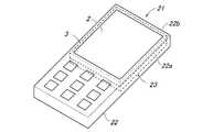
図3は、図1に示したタッチパネル装置1が適用される携帯情報端末を示す斜視図である。この携帯情報端末21では、パネル本体3が、タッチ面2を開放させた状態で筐体22内に収容されている。パネル本体3の背面側には、液晶ディスプレイなどの表示装置23が配置されている。パネル本体3の各部材は透明材料で構成されており、表示装置23の表示画面をパネル本体3を通して見ることができる。 FIG. 3 is a perspective view showing a portable information terminal to which the touch panel device 1 shown in FIG. 1 is applied. In the
本タッチパネル装置1は、後述するように、タッチ面2に対するタッチ操作の他に、パネル本体3の側方からのタッチ操作も検出可能に構成されており、ここで筐体22の側面22a、22bにタッチすることで、予め割り当てられた処理が実行され、例えば筐体22の側面22a上で指をスライドさせることで音量を調整したりあるいは表示画面中のアイコンの選択を切り替えることができる。 As will be described later, the touch panel device 1 is configured to be able to detect a touch operation from the side of the
なお、筐体22の側面22a、22bに対するタッチ操作に割り当てられた処理の内容がわかるように、マークや文字を筐体22に記載したりあるいは表示画面に表示させるようにすると良い。また、携帯情報端末21を把持した際に筐体22の側面22a、22bに指が触れると、これを筐体22の側面22a、22bに対するタッチ操作と誤検知するおそれがあるため、他の操作、例えばタッチ面2に対するタッチ操作がある状態でのみ、筐体22の側面22a、22bに対するタッチ操作が有効となるようにすると良い。また、ユーザにとって操作要領がわかりやすくなるように、筐体22の側面22a、22bにダミーの操作部材を設けるようにしても良い。このようにしても、操作部材の変位を電気的に検出する可変抵抗型のポテンショメータなどの変位検出手段が不要となるため、部品点数を削減して装置の小型化を図ることができる。 It should be noted that marks and characters may be written on the
なお、本タッチパネル装置1を座標入力装置として単体で構成する場合には、図2に示すように筐体9内にパネル本体3が収容される。以降の説明では、この筐体9の側面9a、9bに対するタッチ操作の例を示すが、図3に示すように、表示装置などの他の装置と組み合わせて用いられる場合には、それらの装置も収容する筐体に対するタッチ操作となる。 When the touch panel device 1 is configured as a single unit as a coordinate input device, the
図4は、図1に示した送信部及び受信部の概略構成図である。図5は、図4に示した送信部5の出力信号及び受信部6における各部の出力信号を示す図である。 FIG. 4 is a schematic configuration diagram of the transmission unit and the reception unit illustrated in FIG. FIG. 5 is a diagram illustrating an output signal of the
図4に示すように、送信部5は、パルス発生部31と電極選択部32とを備えている。パルス発生部31では、制御部7から出力されるタイミング信号に同期して駆動信号(パルス信号)を生成する。電極選択部32では、送信電極Y1〜Y5ごとにスイッチング素子が接続されており、送信電極Y1〜Y5を1本ずつ選択して、パルス発生部31から出力される駆動信号を送信電極Y1〜Y5に順次印加する。 As shown in FIG. 4, the
受信部6は、図4に示すように、電極選択部33と受信信号処理部34とを備えている。電極選択部33では、受信電極X1〜X5ごとにスイッチング素子が接続されており、受信電極X1〜X5を1本ずつ選択して、受信電極X1〜X5からの出力信号を受信信号処理部34に順次入力させる。 As shown in FIG. 4, the
ここで、図5(A)に示すように、送信部5は、送信電極Y1〜Y5を1本ずつ選択して所定数の駆動信号(パルス信号)を送信電極Y1〜Y5に順次印加し、送信電極Y1〜Y5の1本に駆動信号を印加する間に、受信部6は、受信電極X1〜X5を1本ずつ選択して受信電極X1〜X5の充放電電流信号を順次受信する。これにより、全ての電極交点ごとの充放電電流信号を取り出すことができる。 Here, as shown in FIG. 5A, the
図4に示したように、受信信号処理部34は、IV変換部41と、バンドパスフィルタ42と、絶対値検出部43と、積分部44と、AD変換部45とを備えている。 As shown in FIG. 4, the reception
IV変換部41では、電極選択部33を介して入力される受信電極X1〜X5の充放電電流信号(アナログ信号)が電圧信号に変換される。バンドパスフィルタ42では、IV変換部41の出力信号に対して、送信電極Y1〜Y5に印加される駆動信号の周波数以外の周波数成分を有する信号を除去する処理が行われる。絶対値検出部(整流部)43では、バンドパスフィルタ42の出力信号に対して全波整流が行われる。積分部44では、絶対値検出部43の出力信号を時間軸方向に積分する処理が行われる。AD変換部45では、積分部44の出力信号をAD変換してレベル信号(ディジタル信号)を出力する。 In the
図5(B)に示したように、送信電極Y1〜Y5に駆動信号(パルス信号)を印加すると、パルス波の立ち上がり及び立ち下がりに応じた充放電電流が受信電極X1〜X5に流れて、これに応じてIV変換部41から出力される電圧信号が所定の振幅で変化するが、タッチ操作があると、電極交点の静電容量が減少するのに伴って、IV変換部41から出力される電圧信号の振幅が小さくなり、積分部44の出力値も小さくなる。 As shown in FIG. 5B, when a drive signal (pulse signal) is applied to the transmission electrodes Y1 to Y5, a charge / discharge current corresponding to the rising and falling of the pulse wave flows to the reception electrodes X1 to X5. In response to this, the voltage signal output from the
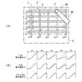
図6、図7、図8は、図1に示したタッチ面2に対するタッチ操作の位置に応じて受信部6の積分部44から出力される信号を示す図である。制御部7では、送信電極Y1〜Y5及び受信電極X1〜X5の選択により電極交点ごとに受信電極X1〜X5から出力される信号に基づいてタッチ面2に対するタッチ位置を検出する。なお、実際には、前記のように、積分部44の出力信号をAD変換して得られたディジタルレベル信号に基づいてタッチ位置の検出が行われる。 6, 7, and 8 are diagrams illustrating signals output from the
図6は、(A)に示すように、タッチ面2における送信電極Y1と受信電極X4との電極交点上をタッチした場合である。この場合、送信電極Y1と受信電極X3、X4、X5との各電極交点の静電容量が減少することから、(B)に示すように、送信電極Y1と受信電極X3、X4、X5の積分部44の各出力値が低下し、その低下幅は、受信電極X4が最も大きく、その両側の受信電極X3、X5の出力値は、受信電極X4の出力値より小さく、受信電極X3と受信電極X4の出力値はほぼ同等程度となる。これにより、出力値の低下がもっとも大きいことから、タッチ位置が、受信電極X4上であることがわかる。 FIG. 6 shows a case where a touch is made on the electrode intersection of the transmission electrode Y1 and the reception electrode X4 on the
また、送信電極Y1に隣り合う送信電極Y2の出力値にも同様の変化が現れるが、この送信電極Y2の出力値の低下幅は送信電極Y1の出力値より小さくなる。これにより、タッチ位置が、送信電極Y1と受信電極X4との電極交点上であることがわかる。 A similar change also appears in the output value of the transmission electrode Y2 adjacent to the transmission electrode Y1, but the width of decrease in the output value of the transmission electrode Y2 is smaller than the output value of the transmission electrode Y1. Thereby, it turns out that a touch position is on the electrode intersection of transmission electrode Y1 and reception electrode X4.
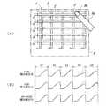
図7は、(A)に示すように、タッチ面2における送信電極Y1上で且つ受信電極X4と受信電極X5との間をタッチした場合である。この場合、送信電極Y1と受信電極X4、X5との各電極交点の静電容量が減少することから、(B)に示すように、送信電極Y1と受信電極X4、X5の積分部44の各出力値が低下し、特にここでは、受信電極X4の出力値の方が受信電極X5の出力値より低下幅が大きいため、タッチ位置は、受信電極X4と受信電極X5との間で、受信電極X4寄りの位置であることがわかる。 FIG. 7 shows a case where a touch is made on the transmission electrode Y1 on the
また、送信電極Y1に隣り合う送信電極Y2の出力値にも同様の変化が現れるが、この送信電極Y2の出力値の低下幅は送信電極Y1の出力値より小さくなる。これにより、タッチ位置が、送信電極Y1上で且つ受信電極X4と受信電極X5との間であることがわかる。 A similar change also appears in the output value of the transmission electrode Y2 adjacent to the transmission electrode Y1, but the width of decrease in the output value of the transmission electrode Y2 is smaller than the output value of the transmission electrode Y1. Thereby, it can be seen that the touch position is on the transmission electrode Y1 and between the reception electrode X4 and the reception electrode X5.
図8は、(A)に示すように、タッチ面2における送信電極Y1と受信電極X5との電極交点上をタッチした場合である。この場合、送信電極Y1と受信電極X4、X5との各電極交点の静電容量が減少することから、(B)に示すように、送信電極Y1と受信電極X4、X5の積分部44の各出力値が低下し、その低下幅は受信電極X5の出力値が大きく、受信電極X4の出力値の低下幅は僅かとなる。これにより、タッチ位置が、受信電極X5上であることがわかる。 FIG. 8 shows a case where a touch is made on the electrode intersection of the transmission electrode Y1 and the reception electrode X5 on the
また、送信電極Y1に隣り合う送信電極Y2の出力値にも同様の変化が現れるが、この送信電極Y2の出力値の低下幅は送信電極Y1の出力値より小さくなる。これにより、タッチ位置が、送信電極Y1と受信電極X5との電極交点上であることがわかる。 A similar change also appears in the output value of the transmission electrode Y2 adjacent to the transmission electrode Y1, but the width of decrease in the output value of the transmission electrode Y2 is smaller than the output value of the transmission electrode Y1. Thereby, it can be seen that the touch position is on the electrode intersection of the transmission electrode Y1 and the reception electrode X5.
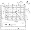
図9、図10は、図1に示したパネル本体3の側方からのタッチ操作の位置に応じて受信部6の積分部44から出力される信号を示す図である。制御部7では、パネル本体3の側縁部9aに近接する最端の受信電極X5とそれに隣り合う受信電極X4に係る信号の変化状況に基づいて、また、パネル本体3の側縁部9bに近接する最端の送信電極Y1とそれに隣り合う送信電極Y2に係る信号の変化状況に基づいて、パネル本体3の側方からのタッチ操作を検知する。 9 and 10 are diagrams illustrating signals output from the integrating
図9は、(A)に示すように、筐体9において受信電極X1〜X5に沿った方向に延在する側面9aにおける送信電極Y1の側方をタッチした場合である。この場合、送信電極Y1と受信電極X5との電極交点の静電容量のみが減少することから、(B)に示すように、送信電極Y1と受信電極X5の積分部44の出力値が低下し、最端の受信電極X5に隣り合う受信電極X4の積分部44の出力値は変化しない。これにより、タッチ位置が、タッチ面2ではなく、筐体9の側面9aであることがわかる。 FIG. 9 shows a case where the side of the transmission electrode Y1 on the
また、送信電極Y1に隣り合う送信電極Y2の出力値にも同様の変化が現れるが、この送信電極Y2の出力値の低下幅は送信電極Y1の出力値より小さくなる。これにより、タッチ位置が、筐体9の側面9aにおける送信電極Y1の側方であることがわかる。 A similar change also appears in the output value of the transmission electrode Y2 adjacent to the transmission electrode Y1, but the width of decrease in the output value of the transmission electrode Y2 is smaller than the output value of the transmission electrode Y1. Thereby, it can be seen that the touch position is the side of the transmission electrode Y <b> 1 on the
図10は、(A)に示すように、筐体9において送信電極Y1〜Y5に沿った方向に延在する側面9bにおける受信電極X4の側方をタッチした場合である。この場合、送信電極Y1と受信電極X3、X4、X5との各電極交点の静電容量のみが減少することから、(B)に示すように、送信電極Y1と受信電極X3、X4、X5の積分部44の各出力値が低下し、最端の送信電極Y1に隣り合う送信電極Y2の積分部44の出力値は変化しない。これにより、タッチ位置が、タッチ面2ではなく、筐体9の側面9bにおける受信電極X4の側方であることがわかる。 FIG. 10 shows a case where the side of the reception electrode X4 on the
なお、このタッチパネル装置1は相互容量方式が採用されているため、図9の例のように筐体9の側面9aに対するタッチ操作と、図10の例のように側面9bに対するタッチ操作とを同時に検出することができるため、側面9a、9bに同時にタッチした場合に、側面9a、9bに個別にタッチした場合とは異なる処理を割り当てることも可能である。 Since the touch panel device 1 employs the mutual capacitance method, the touch operation on the
図11(A)は、図1に示したパネル本体3の別例を示す断面図、図11(B)は、受信電極X1〜X5の配設状況を示す平面図である。ここでは、最端の受信電極X5が、隣り合う受信電極X4に対して、他の受信電極X1〜X4の配置間隔p1より大きい間隔p2をおいて配置されている(p1<p2)。これにより、パネル本体3の側方からのタッチ操作に伴う、最端の受信電極X5に隣り合う受信電極X4の位置での静電容量の変化が小さくなる。このため、タッチ面2に対するタッチ操作と、パネル本体3の側方からのタッチ操作とを精度良く判別することができる。 FIG. 11A is a cross-sectional view showing another example of the
また、最端の受信電極X5が、他の受信電極X1〜X4より太く形成されている(w1<w2)。これにより、最端の受信電極X5の近傍での静電容量の変化に応じた受信電極X5の充放電電流の変化が大きくなるため、パネル本体3の側方からのタッチ操作に対する検知感度が向上する。このため、タッチ面2に対するタッチ操作と、パネル本体3の側方からのタッチ操作とを精度良く判別することができる。 The outermost receiving electrode X5 is formed thicker than the other receiving electrodes X1 to X4 (w1 <w2). As a result, the change in charging / discharging current of the receiving electrode X5 corresponding to the change in capacitance in the vicinity of the outermost receiving electrode X5 is increased, so that the detection sensitivity to the touch operation from the side of the
図12は、図1に示したパネル本体3の別例を示す断面図である。ここでは、保護絶縁体121における最端の受信電極X5の表面側に、タッチ面2が形成された他の表面部分122より厚く形成された肉厚部分123が設けられている。 FIG. 12 is a cross-sectional view showing another example of the
この構成では、最端の受信電極X5の表面側からタッチしたときの指Fと受信電極X5との距離が長くなるため、最端の受信電極X5の表面側からのタッチ操作による静電容量の変化が小さくなり、最端の受信電極X5の表面側からのタッチ操作に対する検知感度が低下する。このため、最端の受信電極X5の積分部44の出力値が所定値未満の場合に受信電極X5の表面側からのタッチ操作、所定値以上の場合に受信電極X5の側方からのタッチ操作と区別することが可能となり、表面側からのタッチ操作を、パネル本体3の側方からのタッチ操作と誤判別することを避けることができる。なお、肉厚部分123は、その表面側が筐体9により覆われてタッチ操作の領域外としても良い。 In this configuration, since the distance between the finger F and the receiving electrode X5 when touched from the surface side of the outermost receiving electrode X5 is increased, the capacitance of the capacitance due to the touch operation from the surface side of the outermost receiving electrode X5 is increased. A change becomes small and the detection sensitivity with respect to the touch operation from the surface side of the outermost receiving electrode X5 falls. For this reason, when the output value of the
図13は、図1に示したパネル本体3の別例を示す断面図である。ここでは、保護絶縁体131における最端の受信電極X5の表面側の部分が、誘電率の低い材料で形成された覆い部分133で覆われている。 FIG. 13 is a cross-sectional view showing another example of the
この構成では、図12の例と同様に、最端の受信電極X5の表面側からのタッチ操作による静電容量の変化が小さくなるため、最端の受信電極X5の表面側からのタッチ操作に対する検知感度が低下する。このため、最端の受信電極X5の積分部44の出力値が所定値未満の場合に受信電極X5の表面側からのタッチ操作、所定値以上の場合に受信電極X5の側方からのタッチ操作と区別することが可能となり、表面側からのタッチ操作を、パネル本体3の側方からのタッチ操作と誤判別することを避けることができる。覆い部分133を形成する誘電率の低い材料としては、例えば発泡樹脂材料などがある。 In this configuration, as in the example of FIG. 12, the change in capacitance due to the touch operation from the surface side of the outermost receiving electrode X5 is reduced, so that the touch operation from the surface side of the outermost receiving electrode X5 is reduced. Detection sensitivity decreases. For this reason, when the output value of the
なお、保護絶縁体における最端の受信電極X5の表面側の部分と筐体との間に空隙を設けるようにしても良い。このようにすると、最端の受信電極X5の表面側に誘電率の低い空気層が介在するため、同様の効果を得ることができる。なお、覆い部分133または空隙は、その表面側が筐体9により覆われてタッチ操作の領域外としても良い。 It should be noted that a gap may be provided between the housing and the surface side portion of the outermost receiving electrode X5 in the protective insulator. In this case, since the air layer having a low dielectric constant is interposed on the surface side of the outermost receiving electrode X5, the same effect can be obtained. Note that the
図14は、図1に示したパネル本体3の別例を示す断面図である。ここでは、保護絶縁体141における最端の受信電極X5の側面側を覆う側面部分143が、他の部分、すなわち送信電極Y1〜Y5及び受信電極X1〜X5の表面側を覆う表面部分142より誘電率の高い材料にて形成されている。 FIG. 14 is a cross-sectional view showing another example of the
この構成では、パネル本体3の側方からのタッチ操作による静電容量の変化が大きくなるため、パネル本体3の側方からのタッチ操作に対する検知感度が向上する。このため、最端の受信電極X5の積分部44の出力値が所定値未満の場合に受信電極X5の表面側からのタッチ操作、所定値以上の場合に受信電極X5の側方からのタッチ操作と区別することが可能となり、表面側からのタッチ操作を、パネル本体3の側方からのタッチ操作と誤判別することを避けることができる。側面部分143を形成する誘電率の高い材料としては、例えばガラス材料や、母材樹脂中に酸化チタン粉末を分散させた複合材料などがある。なお、受信電極X5の表面部分142は、筐体9により覆われてタッチ操作の領域外としても良い。 In this configuration, a change in capacitance due to a touch operation from the side of the
なお、図11〜図14では、筐体9において受信電極X1〜X5に沿った方向に延在する側面9aに対するタッチ操作に影響する最端の受信電極X5に関する例を示したが、図10に示したように、筐体9において送信電極Y1〜Y5に沿った方向に延在する側面9bに対するタッチ操作に影響する最端の送信電極Y1に関して同様の構成を適用することも可能である。 FIGS. 11 to 14 show an example related to the outermost receiving electrode X5 that affects the touch operation on the
図15は、本発明によるタッチパネル装置の別例を示す全体構成図である。なお、パネル本体3の構成は図1に示した例と同様であり、断面の状態も図2に示した例と同様である。 FIG. 15 is an overall configuration diagram showing another example of the touch panel device according to the present invention. The configuration of the
このタッチパネル装置151では、自己容量方式が採用され、Y軸検出部152で検出電極Y1〜Y5を順次選択することで、選択された電極Y1〜Y5を負荷とする弛張発振回路が形成され、タッチ操作に応じて静電容量が増大するのに応じて、検出電極Y1〜Y5から出力される信号の発振周波数が大きくなることを利用してY軸方向のタッチ位置が検出される。 In this
X軸検出部153も、Y軸検出部152と同一の構成となり、X軸検出部153で検出電極X1〜X5を順次選択することで、選択された電極X1〜X5を負荷とする弛張発振回路が形成され、タッチ操作に応じて静電容量が増大するのに応じて、検出電極X1〜X5から出力される信号の発振周波数が大きくなることを利用してX軸方向のタッチ位置が検出される。 The
制御部154では、Y軸検出部152及びX軸検出部153から出力される検出電極Y1〜Y5及び検出電極X1〜X5ごとの信号周波数または信号周期に基づいて2次元のタッチ位置(タッチ領域の中心座標)が求められる。 In the
タッチ面2に対するタッチ操作では、タッチ位置の近傍の複数の検出電極X1〜X5で信号が変化し、一方、パネル本体3の側方からのタッチ操作では、最端の検出電極X5または最端の検出電極Y1のみで信号が変化し、この信号の変化状況に基づいて、タッチ面2に対するタッチ操作とパネル本体3の側方からのタッチ操作とを判別し、さらにタッチ面2上及びパネル本体3の側方のタッチ位置を求めることができる。 In the touch operation on the
因みに、図1に示した相互容量方式による構成では、同時に複数のタッチ位置を検出するマルチタッチが可能であるが、この自己容量方式による構成は、マルチタッチに対応していないため、タッチ面2に対するタッチ操作とパネル本体3の側方からのタッチ操作とを同時に検出することはできない。 Incidentally, in the configuration based on the mutual capacitance method shown in FIG. 1, multi-touch that simultaneously detects a plurality of touch positions is possible. However, since the configuration based on the self-capacitance method does not support multi-touch, the
なお、本タッチパネル装置は、前記のように、座標入力装置として単体で構成したり、あるいはパソコンや携帯情報端末において表示装置と組み合わせて用いることができるが、この他に、大画面の表示装置と組み合わせることで、多人数を対象にしたプレゼンテーションや講義で使用することができるようにした、いわゆるインタラクティブホワイトボード(電子黒板)として用いることも可能である。 As described above, the touch panel device can be configured as a single unit as a coordinate input device, or can be used in combination with a display device in a personal computer or a portable information terminal. By combining them, it can also be used as a so-called interactive whiteboard (electronic blackboard) that can be used in presentations and lectures for a large number of people.
本発明にかかるタッチパネル装置は、装置の側面に操作手段を別途設けることなく、且つ装置の信頼性の低下を招くことなく、装置の側面での操作が可能となる効果を有し、電極が配設された平板状をなすパネル本体の表面側に、ユーザの指などの指示物によるタッチ操作が行われるタッチ面が平面状に形成されたタッチパネル装置などとして有用である。 The touch panel device according to the present invention has an effect that operation on the side surface of the device can be performed without separately providing an operation means on the side surface of the device and without causing deterioration of the reliability of the device. It is useful as a touch panel device or the like in which a touch surface on which a touch operation with an indicator such as a user's finger is performed is formed in a flat shape on the surface side of a flat panel body.
1 タッチパネル装置
2 タッチ面
3 パネル本体
4 位置検出部(制御手段)
5 送信部
6 受信部
7 制御部
9 筐体
9a、9b 側縁部
11 保護絶縁体
12 支持シート
121 保護絶縁体
122 表面部分
123 肉厚部分
131 保護絶縁体
132 表面部分
133 覆い部分
141 保護絶縁体
142 表面部分
143 側面部分
F 指
X1〜X5 受信電極(第2の電極)
Y1〜Y5 送信電極(第1の電極)DESCRIPTION OF SYMBOLS 1
DESCRIPTION OF
Y1 to Y5 transmitting electrode (first electrode)
Claims (6)
Translated fromJapanese前記制御手段は、前記パネル本体の側縁部に近接する最端の電極の前記出力信号が検知された際に、それに隣り合う電極の前記出力信号の出力値が変化しないことに基づいて前記パネル本体の側方からのタッチ操作を検知することを特徴とするタッチパネル装置。A panel body having a flat plate shape in which a plurality of first electrodes that run in parallel to each other and a plurality of second electrodes that run in parallel to each other are arranged in a lattice pattern and a protective insulator having a touch surface is provided on the surface side thereof And a control means for detecting a touch position based on a change in an output signal of the electrode in accordance with a change in capacitance according to a touch operation on the touch surface,
When theoutput signal of the outermost electrode adjacent to the side edge of the panel bodyis detected , the control means is based on thefact thatthe output value of the output signal of the adjacent electrodedoes not change. A touch panel device that detects a touch operation from a side of a main body.
前記保護絶縁体における最端の電極の表面側の部分が、他の部分より厚く形成されたことを特徴とする請求項1乃至請求項4のいずれかに記載のタッチパネル装置。The panel body includes a protective insulator for protecting the first electrode and the second electrode on the surface side thereof,
5. The touch panel device according to claim 1, wherein a portion on the surface side of the outermost electrode in the protective insulator is formed to be thicker than other portions.
前記保護絶縁体における前記最端の電極の側面側を覆う部分が、他の部分より誘電率の高い材料にて形成されたことを特徴とする請求項1乃至請求項5のいずれかに記載のタッチパネル装置。The panel body includes a protective insulator for protecting the first electrode and the second electrode on the surface side and the side surface thereof,
The part covering the side surface side of the outermost electrode in the protective insulator is formed of a material having a higher dielectric constant than the other part. Touch panel device.
Priority Applications (2)
| Application Number | Priority Date | Filing Date | Title |
|---|---|---|---|
| JP2010037078AJP5264800B2 (en) | 2010-02-23 | 2010-02-23 | Touch panel device |
| US13/024,819US20110205172A1 (en) | 2010-02-23 | 2011-02-10 | Touch screen device |
Applications Claiming Priority (1)
| Application Number | Priority Date | Filing Date | Title |
|---|---|---|---|
| JP2010037078AJP5264800B2 (en) | 2010-02-23 | 2010-02-23 | Touch panel device |
Related Child Applications (1)
| Application Number | Title | Priority Date | Filing Date |
|---|---|---|---|
| JP2013093409ADivisionJP2013145603A (en) | 2013-04-26 | 2013-04-26 | Touch panel device |
Publications (2)
| Publication Number | Publication Date |
|---|---|
| JP2011175335A JP2011175335A (en) | 2011-09-08 |
| JP5264800B2true JP5264800B2 (en) | 2013-08-14 |
Family
ID=44476099
Family Applications (1)
| Application Number | Title | Priority Date | Filing Date |
|---|---|---|---|
| JP2010037078AExpired - Fee RelatedJP5264800B2 (en) | 2010-02-23 | 2010-02-23 | Touch panel device |
Country Status (2)
| Country | Link |
|---|---|
| US (1) | US20110205172A1 (en) |
| JP (1) | JP5264800B2 (en) |
Families Citing this family (22)
| Publication number | Priority date | Publication date | Assignee | Title |
|---|---|---|---|---|
| US8902191B2 (en)* | 2009-01-28 | 2014-12-02 | Synaptics Incorporated | Proximity sensing for capacitive touch sensors |
| JP4897983B1 (en) | 2011-05-18 | 2012-03-14 | パナソニック株式会社 | Touch panel device and indicator distinguishing method |
| DE102011078077A1 (en)* | 2011-06-24 | 2012-12-27 | Ident Technology Ag | Printed circuit board with electrode configuration of a capacitive sensor |
| US9244574B2 (en)* | 2011-10-11 | 2016-01-26 | Synaptics Incorporated | Reducing ion-migration and corrosion in electrodes |
| FR2990020B1 (en)* | 2012-04-25 | 2014-05-16 | Fogale Nanotech | CAPACITIVE DETECTION DEVICE WITH ARRANGEMENT OF CONNECTION TRACKS, AND METHOD USING SUCH A DEVICE. |
| CN104603729B (en)* | 2012-04-27 | 2018-02-02 | 阿尔申蒂斯有限责任公司 | Apparatus for determining touch input stimuli |
| JP5347096B1 (en)* | 2012-09-13 | 2013-11-20 | 株式会社ワンダーフューチャーコーポレーション | Touch panel manufacturing method, touch panel, and input / output integrated device including touch panel and display device |
| JP2014174760A (en)* | 2013-03-08 | 2014-09-22 | Japan Display Inc | Display device attached with touch detection function, and electronic device |
| US20140267137A1 (en)* | 2013-03-14 | 2014-09-18 | Synaptics Incorporated | Proximity sensing using driven ground plane |
| JP6121242B2 (en)* | 2013-05-27 | 2017-04-26 | アルプス電気株式会社 | Input device |
| JP5470489B2 (en)* | 2013-06-24 | 2014-04-16 | 株式会社ワンダーフューチャーコーポレーション | Touch panel, touch panel manufacturing method, and touch panel integrated display device |
| JP6087244B2 (en)* | 2013-09-04 | 2017-03-01 | アルパイン株式会社 | Position detection device |
| WO2015038133A1 (en)* | 2013-09-12 | 2015-03-19 | Intel Corporation | Detecting gestures on the side of a computing device |
| KR20160057346A (en)* | 2013-09-17 | 2016-05-23 | 에이브이씨 테크놀로지 가부시키가이샤 | Touch panel device and method for driving touch panel |
| JP6290705B2 (en)* | 2013-09-24 | 2018-03-07 | アルプス電気株式会社 | Input device |
| CN103543385A (en)* | 2013-10-15 | 2014-01-29 | 苏州泛普纳米科技有限公司 | Automatic test device and method of inducting unit |
| JP5739554B2 (en)* | 2014-01-29 | 2015-06-24 | 株式会社ワンダーフューチャーコーポレーション | Touch panel, touch panel manufacturing method, and touch panel integrated display device |
| US20170024124A1 (en)* | 2014-04-14 | 2017-01-26 | Sharp Kabushiki Kaisha | Input device, and method for controlling input device |
| WO2016056516A1 (en)* | 2014-10-10 | 2016-04-14 | シャープ株式会社 | Display device |
| KR102297484B1 (en)* | 2015-01-16 | 2021-09-02 | 삼성디스플레이 주식회사 | Display device and driving method thereof |
| JP6565856B2 (en)* | 2016-10-05 | 2019-08-28 | 株式会社デンソー | Touch input device |
| WO2018089920A1 (en)* | 2016-11-14 | 2018-05-17 | The Regents Of The University Of Colorado, A Body Corporate | Method and apparatus for battery-free identification token for touch sensing devices |
Family Cites Families (8)
| Publication number | Priority date | Publication date | Assignee | Title |
|---|---|---|---|---|
| NZ331543A (en)* | 1996-12-10 | 2000-05-26 | Touchsensor Technologies L | Differential proximity sensor and output circuit |
| US7800592B2 (en)* | 2005-03-04 | 2010-09-21 | Apple Inc. | Hand held electronic device with multiple touch sensing devices |
| EP1087286A4 (en)* | 1998-06-08 | 2007-10-17 | Kaneka Corp | Resistor film touch panel used for liquid crystal display and liquid crystal display with the same |
| AU2002321680A1 (en)* | 2001-06-29 | 2003-01-21 | Hans Rudolf Sterling | Apparatus for sensing the position of a pointing object |
| US7944436B2 (en)* | 2006-04-28 | 2011-05-17 | Hewlett-Packard Development Company, L.P. | Protective layer for use in computing devices with touch-sensitive surfaces |
| JP2008197934A (en)* | 2007-02-14 | 2008-08-28 | Calsonic Kansei Corp | Operator determining method |
| US9323398B2 (en)* | 2009-07-10 | 2016-04-26 | Apple Inc. | Touch and hover sensing |
| TWI408441B (en)* | 2009-12-09 | 2013-09-11 | Au Optronics Corp | Touch display panel and touch substrate |
- 2010
- 2010-02-23JPJP2010037078Apatent/JP5264800B2/ennot_activeExpired - Fee Related
- 2011
- 2011-02-10USUS13/024,819patent/US20110205172A1/ennot_activeAbandoned
Also Published As
| Publication number | Publication date |
|---|---|
| JP2011175335A (en) | 2011-09-08 |
| US20110205172A1 (en) | 2011-08-25 |
Similar Documents
| Publication | Publication Date | Title |
|---|---|---|
| JP5264800B2 (en) | Touch panel device | |
| US10261628B2 (en) | Driving chip, circuit film, chip-on-film type driving circuit, and display device having built-in touchscreen | |
| CN105637458B (en) | Single layer sensor pattern | |
| EP2638458B1 (en) | Touch device for determining real coordinates of multiple touch points and method thereof | |
| CN114846432B (en) | Tactile presentation control device, tactile presentation panel, tactile presentation touch panel, and tactile presentation touch display | |
| JP4850946B2 (en) | Touch panel device | |
| WO2009000289A1 (en) | Improvements in or relating to user interfaces and associated apparatus and methods | |
| WO2010102470A1 (en) | Pressure sensitive touch control device | |
| TW201619796A (en) | Electrode arrangement for gesture detection and tracking | |
| US9146643B2 (en) | Touch sensing apparatus and method thereof | |
| JP4913859B2 (en) | Touch panel device | |
| JP4913883B2 (en) | Touch panel device | |
| US20130155003A1 (en) | Touch sensing apparatus and method thereof | |
| TW201207682A (en) | Position detection apparatus, sensor and position detection method | |
| JP2013145603A (en) | Touch panel device | |
| JP7267916B2 (en) | POSITION DETECTION SENSOR, POSITION DETECTION DEVICE, AND INFORMATION PROCESSING SYSTEM | |
| JP4944975B2 (en) | Touch panel device | |
| US11861112B2 (en) | Touch sensor panel | |
| KR101525674B1 (en) | Touchscreen apparatus and driving method thereof | |
| TW201344544A (en) | Touch panel device having a divided ITO layer for reducing loading | |
| US20150153869A1 (en) | Touchscreen device | |
| CN102609159A (en) | Capacitive touch device, sensing device thereof and multi-touch detection method | |
| JP6772658B2 (en) | Capacitive input device | |
| KR20150006328A (en) | Touchscreen apparatus | |
| EP2423794A2 (en) | Pointer detection apparatus, position detector sensor, and manufacturing method for position detection sensor |
Legal Events
| Date | Code | Title | Description |
|---|---|---|---|
| RD02 | Notification of acceptance of power of attorney | Free format text:JAPANESE INTERMEDIATE CODE: A7422 Effective date:20110822 | |
| A621 | Written request for application examination | Free format text:JAPANESE INTERMEDIATE CODE: A621 Effective date:20121002 | |
| A871 | Explanation of circumstances concerning accelerated examination | Free format text:JAPANESE INTERMEDIATE CODE: A871 Effective date:20121002 | |
| A975 | Report on accelerated examination | Free format text:JAPANESE INTERMEDIATE CODE: A971005 Effective date:20121022 | |
| A131 | Notification of reasons for refusal | Free format text:JAPANESE INTERMEDIATE CODE: A131 Effective date:20130115 | |
| A521 | Written amendment | Free format text:JAPANESE INTERMEDIATE CODE: A523 Effective date:20130312 | |
| TRDD | Decision of grant or rejection written | ||
| A01 | Written decision to grant a patent or to grant a registration (utility model) | Free format text:JAPANESE INTERMEDIATE CODE: A01 Effective date:20130402 | |
| A61 | First payment of annual fees (during grant procedure) | Free format text:JAPANESE INTERMEDIATE CODE: A61 Effective date:20130430 | |
| R150 | Certificate of patent or registration of utility model | Free format text:JAPANESE INTERMEDIATE CODE: R150 | |
| LAPS | Cancellation because of no payment of annual fees |