JP5258566B2 - Manufacturing method of surface acoustic wave device - Google Patents
Manufacturing method of surface acoustic wave deviceDownload PDFInfo
- Publication number
- JP5258566B2 JP5258566B2JP2008528827AJP2008528827AJP5258566B2JP 5258566 B2JP5258566 B2JP 5258566B2JP 2008528827 AJP2008528827 AJP 2008528827AJP 2008528827 AJP2008528827 AJP 2008528827AJP 5258566 B2JP5258566 B2JP 5258566B2
- Authority
- JP
- Japan
- Prior art keywords
- acoustic wave
- surface acoustic
- wave device
- manufacturing
- film
- Prior art date
- Legal status (The legal status is an assumption and is not a legal conclusion. Google has not performed a legal analysis and makes no representation as to the accuracy of the status listed.)
- Active
Links
Images


Classifications
- H—ELECTRICITY
- H03—ELECTRONIC CIRCUITRY
- H03H—IMPEDANCE NETWORKS, e.g. RESONANT CIRCUITS; RESONATORS
- H03H3/00—Apparatus or processes specially adapted for the manufacture of impedance networks, resonating circuits, resonators
- H03H3/007—Apparatus or processes specially adapted for the manufacture of impedance networks, resonating circuits, resonators for the manufacture of electromechanical resonators or networks
- H03H3/08—Apparatus or processes specially adapted for the manufacture of impedance networks, resonating circuits, resonators for the manufacture of electromechanical resonators or networks for the manufacture of resonators or networks using surface acoustic waves
- H—ELECTRICITY
- H03—ELECTRONIC CIRCUITRY
- H03H—IMPEDANCE NETWORKS, e.g. RESONANT CIRCUITS; RESONATORS
- H03H3/00—Apparatus or processes specially adapted for the manufacture of impedance networks, resonating circuits, resonators
- H03H3/007—Apparatus or processes specially adapted for the manufacture of impedance networks, resonating circuits, resonators for the manufacture of electromechanical resonators or networks
- H—ELECTRICITY
- H03—ELECTRONIC CIRCUITRY
- H03H—IMPEDANCE NETWORKS, e.g. RESONANT CIRCUITS; RESONATORS
- H03H9/00—Networks comprising electromechanical or electro-acoustic elements; Electromechanical resonators
- H03H9/0023—Networks for transforming balanced signals into unbalanced signals and vice versa, e.g. baluns, or networks having balanced input and output
- H03H9/0028—Networks for transforming balanced signals into unbalanced signals and vice versa, e.g. baluns, or networks having balanced input and output using surface acoustic wave devices
- H03H9/008—Networks for transforming balanced signals into unbalanced signals and vice versa, e.g. baluns, or networks having balanced input and output using surface acoustic wave devices having three acoustic tracks
- H—ELECTRICITY
- H03—ELECTRONIC CIRCUITRY
- H03H—IMPEDANCE NETWORKS, e.g. RESONANT CIRCUITS; RESONATORS
- H03H9/00—Networks comprising electromechanical or electro-acoustic elements; Electromechanical resonators
- H03H9/02—Details
- H03H9/05—Holders or supports
- H03H9/0538—Constructional combinations of supports or holders with electromechanical or other electronic elements
- H03H9/0566—Constructional combinations of supports or holders with electromechanical or other electronic elements for duplexers
- H03H9/0576—Constructional combinations of supports or holders with electromechanical or other electronic elements for duplexers including surface acoustic wave [SAW] devices
- H—ELECTRICITY
- H03—ELECTRONIC CIRCUITRY
- H03H—IMPEDANCE NETWORKS, e.g. RESONANT CIRCUITS; RESONATORS
- H03H9/00—Networks comprising electromechanical or electro-acoustic elements; Electromechanical resonators
- H03H9/02—Details
- H03H9/05—Holders or supports
- H03H9/058—Holders or supports for surface acoustic wave devices
- H03H9/059—Holders or supports for surface acoustic wave devices consisting of mounting pads or bumps
- H—ELECTRICITY
- H03—ELECTRONIC CIRCUITRY
- H03H—IMPEDANCE NETWORKS, e.g. RESONANT CIRCUITS; RESONATORS
- H03H9/00—Networks comprising electromechanical or electro-acoustic elements; Electromechanical resonators
- H03H9/02—Details
- H03H9/05—Holders or supports
- H03H9/10—Mounting in enclosures
- H03H9/1064—Mounting in enclosures for surface acoustic wave [SAW] devices
- H03H9/1071—Mounting in enclosures for surface acoustic wave [SAW] devices the enclosure being defined by a frame built on a substrate and a cap, the frame having no mechanical contact with the SAW device
- H—ELECTRICITY
- H03—ELECTRONIC CIRCUITRY
- H03H—IMPEDANCE NETWORKS, e.g. RESONANT CIRCUITS; RESONATORS
- H03H9/00—Networks comprising electromechanical or electro-acoustic elements; Electromechanical resonators
- H03H9/02—Details
- H03H9/05—Holders or supports
- H03H9/10—Mounting in enclosures
- H03H9/1064—Mounting in enclosures for surface acoustic wave [SAW] devices
- H03H9/1092—Mounting in enclosures for surface acoustic wave [SAW] devices the enclosure being defined by a cover cap mounted on an element forming part of the surface acoustic wave [SAW] device on the side of the IDT's
- H—ELECTRICITY
- H03—ELECTRONIC CIRCUITRY
- H03H—IMPEDANCE NETWORKS, e.g. RESONANT CIRCUITS; RESONATORS
- H03H9/00—Networks comprising electromechanical or electro-acoustic elements; Electromechanical resonators
- H03H9/02—Details
- H03H9/125—Driving means, e.g. electrodes, coils
- H03H9/145—Driving means, e.g. electrodes, coils for networks using surface acoustic waves
- H03H9/14544—Transducers of particular shape or position
- H03H9/14576—Transducers whereby only the last fingers have different characteristics with respect to the other fingers, e.g. different shape, thickness or material, split finger
- H03H9/14582—Transducers whereby only the last fingers have different characteristics with respect to the other fingers, e.g. different shape, thickness or material, split finger the last fingers having a different pitch
- H—ELECTRICITY
- H05—ELECTRIC TECHNIQUES NOT OTHERWISE PROVIDED FOR
- H05K—PRINTED CIRCUITS; CASINGS OR CONSTRUCTIONAL DETAILS OF ELECTRIC APPARATUS; MANUFACTURE OF ASSEMBLAGES OF ELECTRICAL COMPONENTS
- H05K1/00—Printed circuits
- H05K1/02—Details
- H05K1/14—Structural association of two or more printed circuits
- H05K1/144—Stacked arrangements of planar printed circuit boards
- H—ELECTRICITY
- H05—ELECTRIC TECHNIQUES NOT OTHERWISE PROVIDED FOR
- H05K—PRINTED CIRCUITS; CASINGS OR CONSTRUCTIONAL DETAILS OF ELECTRIC APPARATUS; MANUFACTURE OF ASSEMBLAGES OF ELECTRICAL COMPONENTS
- H05K3/00—Apparatus or processes for manufacturing printed circuits
- H05K3/30—Assembling printed circuits with electric components, e.g. with resistor
- H05K3/32—Assembling printed circuits with electric components, e.g. with resistor electrically connecting electric components or wires to printed circuits
- H05K3/34—Assembling printed circuits with electric components, e.g. with resistor electrically connecting electric components or wires to printed circuits by soldering
- H05K3/341—Surface mounted components
- H05K3/3421—Leaded components
- H05K3/3426—Leaded components characterised by the leads
- H—ELECTRICITY
- H10—SEMICONDUCTOR DEVICES; ELECTRIC SOLID-STATE DEVICES NOT OTHERWISE PROVIDED FOR
- H10N—ELECTRIC SOLID-STATE DEVICES NOT OTHERWISE PROVIDED FOR
- H10N30/00—Piezoelectric or electrostrictive devices
- H10N30/01—Manufacture or treatment
- H10N30/02—Forming enclosures or casings
- H—ELECTRICITY
- H10—SEMICONDUCTOR DEVICES; ELECTRIC SOLID-STATE DEVICES NOT OTHERWISE PROVIDED FOR
- H10N—ELECTRIC SOLID-STATE DEVICES NOT OTHERWISE PROVIDED FOR
- H10N30/00—Piezoelectric or electrostrictive devices
- H10N30/01—Manufacture or treatment
- H10N30/05—Manufacture of multilayered piezoelectric or electrostrictive devices, or parts thereof, e.g. by stacking piezoelectric bodies and electrodes
- H—ELECTRICITY
- H01—ELECTRIC ELEMENTS
- H01L—SEMICONDUCTOR DEVICES NOT COVERED BY CLASS H10
- H01L2224/00—Indexing scheme for arrangements for connecting or disconnecting semiconductor or solid-state bodies and methods related thereto as covered by H01L24/00
- H01L2224/01—Means for bonding being attached to, or being formed on, the surface to be connected, e.g. chip-to-package, die-attach, "first-level" interconnects; Manufacturing methods related thereto
- H01L2224/10—Bump connectors; Manufacturing methods related thereto
- H01L2224/11—Manufacturing methods
- H—ELECTRICITY
- H01—ELECTRIC ELEMENTS
- H01L—SEMICONDUCTOR DEVICES NOT COVERED BY CLASS H10
- H01L2224/00—Indexing scheme for arrangements for connecting or disconnecting semiconductor or solid-state bodies and methods related thereto as covered by H01L24/00
- H01L2224/93—Batch processes
- H01L2224/94—Batch processes at wafer-level, i.e. with connecting carried out on a wafer comprising a plurality of undiced individual devices
- H—ELECTRICITY
- H01—ELECTRIC ELEMENTS
- H01L—SEMICONDUCTOR DEVICES NOT COVERED BY CLASS H10
- H01L2924/00—Indexing scheme for arrangements or methods for connecting or disconnecting semiconductor or solid-state bodies as covered by H01L24/00
- H01L2924/15—Details of package parts other than the semiconductor or other solid state devices to be connected
- H01L2924/161—Cap
- H01L2924/162—Disposition
- H01L2924/16235—Connecting to a semiconductor or solid-state bodies, i.e. cap-to-chip
- H—ELECTRICITY
- H03—ELECTRONIC CIRCUITRY
- H03H—IMPEDANCE NETWORKS, e.g. RESONANT CIRCUITS; RESONATORS
- H03H3/00—Apparatus or processes specially adapted for the manufacture of impedance networks, resonating circuits, resonators
- H03H3/007—Apparatus or processes specially adapted for the manufacture of impedance networks, resonating circuits, resonators for the manufacture of electromechanical resonators or networks
- H03H2003/0071—Apparatus or processes specially adapted for the manufacture of impedance networks, resonating circuits, resonators for the manufacture of electromechanical resonators or networks of bulk acoustic wave and surface acoustic wave elements in the same process
- Y—GENERAL TAGGING OF NEW TECHNOLOGICAL DEVELOPMENTS; GENERAL TAGGING OF CROSS-SECTIONAL TECHNOLOGIES SPANNING OVER SEVERAL SECTIONS OF THE IPC; TECHNICAL SUBJECTS COVERED BY FORMER USPC CROSS-REFERENCE ART COLLECTIONS [XRACs] AND DIGESTS
- Y10—TECHNICAL SUBJECTS COVERED BY FORMER USPC
- Y10T—TECHNICAL SUBJECTS COVERED BY FORMER US CLASSIFICATION
- Y10T29/00—Metal working
- Y10T29/42—Piezoelectric device making
- Y—GENERAL TAGGING OF NEW TECHNOLOGICAL DEVELOPMENTS; GENERAL TAGGING OF CROSS-SECTIONAL TECHNOLOGIES SPANNING OVER SEVERAL SECTIONS OF THE IPC; TECHNICAL SUBJECTS COVERED BY FORMER USPC CROSS-REFERENCE ART COLLECTIONS [XRACs] AND DIGESTS
- Y10—TECHNICAL SUBJECTS COVERED BY FORMER USPC
- Y10T—TECHNICAL SUBJECTS COVERED BY FORMER US CLASSIFICATION
- Y10T29/00—Metal working
- Y10T29/49—Method of mechanical manufacture
- Y10T29/49002—Electrical device making
- Y10T29/49005—Acoustic transducer
- Y—GENERAL TAGGING OF NEW TECHNOLOGICAL DEVELOPMENTS; GENERAL TAGGING OF CROSS-SECTIONAL TECHNOLOGIES SPANNING OVER SEVERAL SECTIONS OF THE IPC; TECHNICAL SUBJECTS COVERED BY FORMER USPC CROSS-REFERENCE ART COLLECTIONS [XRACs] AND DIGESTS
- Y10—TECHNICAL SUBJECTS COVERED BY FORMER USPC
- Y10T—TECHNICAL SUBJECTS COVERED BY FORMER US CLASSIFICATION
- Y10T29/00—Metal working
- Y10T29/49—Method of mechanical manufacture
- Y10T29/49002—Electrical device making
- Y10T29/49117—Conductor or circuit manufacturing
- Y10T29/49124—On flat or curved insulated base, e.g., printed circuit, etc.
- Y10T29/4913—Assembling to base an electrical component, e.g., capacitor, etc.
- Y10T29/49144—Assembling to base an electrical component, e.g., capacitor, etc. by metal fusion
- Y—GENERAL TAGGING OF NEW TECHNOLOGICAL DEVELOPMENTS; GENERAL TAGGING OF CROSS-SECTIONAL TECHNOLOGIES SPANNING OVER SEVERAL SECTIONS OF THE IPC; TECHNICAL SUBJECTS COVERED BY FORMER USPC CROSS-REFERENCE ART COLLECTIONS [XRACs] AND DIGESTS
- Y10—TECHNICAL SUBJECTS COVERED BY FORMER USPC
- Y10T—TECHNICAL SUBJECTS COVERED BY FORMER US CLASSIFICATION
- Y10T29/00—Metal working
- Y10T29/49—Method of mechanical manufacture
- Y10T29/49002—Electrical device making
- Y10T29/49117—Conductor or circuit manufacturing
- Y10T29/49124—On flat or curved insulated base, e.g., printed circuit, etc.
- Y10T29/49155—Manufacturing circuit on or in base
Landscapes
- Physics & Mathematics (AREA)
- Acoustics & Sound (AREA)
- Engineering & Computer Science (AREA)
- Manufacturing & Machinery (AREA)
- Microelectronics & Electronic Packaging (AREA)
- Surface Acoustic Wave Elements And Circuit Networks Thereof (AREA)
Description
Translated fromJapanese本発明は、移動体通信機器等の無線通信回路に主に用いられる弾性表面波装置の製造方法に関し、特に表面実装可能な弾性表面波装置を小型化可能であるとともにウエハプロセスでパッケージングまで行うことが可能な弾性表面波装置の製造方法に関する。 The present invention relates to a method of manufacturing a surface acoustic wave device mainly used in a radio communication circuit such as a mobile communication device, and more particularly to a surface mountable surface acoustic wave device that can be downsized and packaged by a wafer process. The present invention relates to a method for manufacturing a surface acoustic wave device that can perform the above-described process.
近年、移動体通信に用いられる携帯端末装置は、小型化、軽量化が進むとともに、複数の通信システムに対応するマルチバンド化及び携帯端末装置の多機能化のため、内蔵される回路が増加してきている。そのため、使用される電子部品は、その実装密度向上のため、表面実装可能な小型部品とすることが強く要望されている。 In recent years, mobile terminal devices used for mobile communication have been reduced in size and weight, and the number of built-in circuits has been increased due to the multi-band and multi-functionality of mobile terminal devices corresponding to a plurality of communication systems. ing. For this reason, there is a strong demand for electronic parts to be used as small parts that can be surface-mounted in order to improve the mounting density.
一方、携帯端末装置のキーパーツとして弾性表面波装置がある。弾性表面波装置では、弾性表面波が励振される電極面近傍に中空部を設け、振動空間を確保するとともに、この振動空間を気密封止する必要がある。このため、弾性表面波装置は、例えば、セラミックパッケージに収容されていた。このような弾性表面波装置においても、低損失で優れた通過帯域外の遮断特性を有するとともに、表面実装可能な小型の弾性表面波装置が要求されている。 On the other hand, there is a surface acoustic wave device as a key part of a portable terminal device. In the surface acoustic wave device, it is necessary to provide a hollow portion near the electrode surface where the surface acoustic wave is excited to secure a vibration space and to hermetically seal the vibration space. For this reason, the surface acoustic wave device is accommodated in, for example, a ceramic package. Also in such a surface acoustic wave device, there is a demand for a small surface acoustic wave device that has low loss and excellent cutoff characteristics outside the passband and that can be surface-mounted.
この小型化の要求に対して、WLP(Wafer Level Package)タイプの表面実装構造の弾性表面波装置が提案されている(例えば、特開平9−172339号公報、特表2005−537661号公報を参照)。 In response to this demand for miniaturization, surface acoustic wave devices having a surface mounting structure of WLP (Wafer Level Package) type have been proposed (see, for example, JP-A-9-172339 and JP-T-2005-537661). ).
図9は、従来の弾性表面波装置の製造方法を説明する図である。従来の弾性表面波装置の製造方法においては、まず、図9(a)に示すように、圧電基板961の上に形成した弾性表面波素子の電極パターン962の表面を覆い、電極パターン962に接続された電極パッド968の少なくとも一部を露出させるように、ポリシリコン、アモルファスシリコン等からなる犠牲層963を形成する。次に、図9(b)に示すように、犠牲層963を覆うように保護カバー964を形成した後、保護カバー964に、内部の犠牲層963を露出させる貫通孔965を形成する。次に、図9(c)に示すように、犠牲層963をドライエッチング法等により貫通孔965を通して除去して、電極パターン962の上に中空部966を形成し、弾性表面波装置を得る。 FIG. 9 is a diagram for explaining a conventional method of manufacturing a surface acoustic wave device. In the conventional method for manufacturing a surface acoustic wave device, first, as shown in FIG. 9A, the surface of the
しかしながら、図9に示すように、犠牲層963を用いて保護カバー964を形成する場合、犠牲層963を除去する工程において、中空部966に残留するエッチャント及びエッチング生成物の影響で、弾性表面波装置の電気特性が劣化する問題点があった。 However, as shown in FIG. 9, when the
さらに、中空部966を形成するための製造工程において工数が多く、製造工程が複雑となる問題点があった。 Further, there are problems in that the manufacturing process for forming the
本発明は上述の問題点を解決するために案出されたものであり、その目的は、犠牲層を用いずに中空部を設けることで、電気特性の劣化を低減することができる弾性表面波装置の製造方法を提供することにある。また、中空部を製造するための製造工程の工数を少なくすることができる弾性表面波装置の製造方法を提供することにある。 The present invention has been devised to solve the above-described problems, and its purpose is to provide a surface acoustic wave that can reduce deterioration of electrical characteristics by providing a hollow portion without using a sacrificial layer. It is to provide a method for manufacturing an apparatus. Moreover, it is providing the manufacturing method of the surface acoustic wave apparatus which can reduce the man-hour of the manufacturing process for manufacturing a hollow part.
本発明の上記課題を解決するため、第1の態様に係る弾性表面波装置の製造方法は、(a) 圧電基板の上面にIDT電極及び前記IDT電極と外部回路とを接続するための接続線を形成する工程と、(b) 前記圧電基板の上に前記IDT電極が形成された形成領域を囲み前記接続線を跨ぐ部分を有する枠体を形成する工程と、(c) 前記枠体の上面にフィルム状の蓋体を載置して前記枠体と接合することにより、前記形成領域を覆うとともに前記形成領域との間に密閉空間を設けるための、前記枠体と前記蓋体とで構成される保護カバーを形成する工程と、(e) 前記保護カバーが形成された1枚のウエハ状の前記圧電基板を覆うメッキ用下地層を形成する工程と、(f) 前記保護カバーの外側に位置する前記接続線の上に開口部を有するメッキ用レジスト膜を前記メッキ用下地層の上に形成する工程と、(g) 前記開口部の底に露出する前記メッキ用下地層の上に、メッキ法により柱状電極を形成する工程と、(h) 前記柱状電極を残し、前記メッキ用レジスト膜と前記メッキ用下地層とを除去する工程と、(i) 前記圧電基板の上に、前記保護カバーと前記柱状電極とを覆う封止樹脂膜を形成する工程と、(j) 前記封止樹脂膜の上面を研削して、前記柱状電極を露出させる工程と、を有する。第1の態様に係る弾性表面波装置の製造方法は、(d) 前記工程(a)の後であって前記工程(b)の前に、前記IDT電極及び前記圧電基板の上面の前記枠体が配置される領域を覆い前記枠体と前記接続線との間に介在する保護膜を形成する工程と、(l) 前記工程(i)の後であって前記外部回路との接続前に、前記圧電基板の下面に、前記封止樹脂膜と熱膨張係数が略同一の材料からなる保護層を形成する工程と、をさらに有する。In order to solve the above-described problems of the present invention, a surface acoustic wave device manufacturing method according to a first aspect includes (a) an IDT electrode on a top surface of a piezoelectric substrate, and a connection line for connecting the IDT electrode and an external circuit. And (b) forming a frame having a portion surrounding the connection line and surrounding the formation region where the IDT electrode is formed on the piezoelectric substrate, and (c) an upper surface of the frame A film-like lid is placed on and joined to the frame to cover the formation region and provide a sealed space between the formation region and the frame and the lid Forming a protective cover;(e) forming a plating base layer that covers the one wafer-like piezoelectric substrate on which the protective cover is formed; and (f) outside the protective cover. A resist film for plating having an opening on the connection line located Forming on the plating base layer, and (g) forming a columnar electrode on the plating base layer exposed at the bottom of the opening by plating, and (h) the columnar electrode. And removing the plating resist film and the plating base layer, and (i) forming a sealing resin film covering the protective cover and the columnar electrode on the piezoelectric substrate; (J) grinding the upper surface of the sealing resin film to expose the columnar electrode . The surface acoustic wave device manufacturing method according to the first aspect includes (d) the frame on the upper surface of the IDT electrode and the piezoelectric substrate after the step (a) and before the step (b). there forminga protective film interposed between the frame body covers a region disposed between said connecting line,before connection to the external circuit even after the (l) said step (i), Forming a protective layer made of a material having substantially the same thermal expansion coefficient as that of the sealing resin film on the lower surface of the piezoelectric substrate .
第1の態様によれば、犠牲層を用いることなく形成領域と保護カバーとの間に密閉空間を形成することができるので、電気特性の劣化を低減した弾性表面波装置を製造することができる。 According to the first aspect, since a sealed space can be formed between the formation region and the protective cover without using a sacrificial layer, a surface acoustic wave device with reduced deterioration in electrical characteristics can be manufactured. .
また、犠牲層を用いることなく第1の領域と保護カバーとの間に密閉空間を形成することができるので、密閉空間を形成するための工数を少なくすることができ、生産性を向上することができる。さらに、枠体の被形成面への密着性を向上することができ、弾性表面波装置の信頼性を向上することができる。加えて、密閉空間を封止した状態で、外部回路にあわせて接続線の位置を自由に決定することができる。このため、汎用性の高い弾性表面波装置を製造することができる。第1の態様によれば、表面実装可能な弾性表面波装置を提供することができる。また、弾性表面波装置をウエハレベルで製造することできるので、複雑な工程を経ることなく弾性表面波装置を提供することができる。第1の態様によれば、製造時及び製造後における弾性表面波装置の耐衝撃性を向上させることができる。そのため、弾性表面波装置の割れ、カケ等の不良の発生を抑制し、歩留まりを向上し、弾性表面波装置の信頼性を向上することができる。In addition, since a sealed space can be formed between the first region and the protective cover without using a sacrificial layer, man-hours for forming the sealed space can be reduced, and productivity can be improved. Can do. Furthermore, the adhesion of the frame to the surface to be formed can be improved, and the reliability of the surface acoustic wave device can be improved. In addition, the position of the connection line can be freely determined in accordance with the external circuit while the sealed space is sealed. For this reason, a highly versatile surface acoustic wave device can be manufactured.According to the first aspect, a surface acoustic wave device capable of surface mounting can be provided. In addition, since the surface acoustic wave device can be manufactured at the wafer level, the surface acoustic wave device can be provided without complicated processes. According to the 1st aspect, the impact resistance of the surface acoustic wave apparatus at the time of manufacture and after manufacture can be improved. Therefore, the occurrence of defects such as cracking and chipping of the surface acoustic wave device can be suppressed, the yield can be improved, and the reliability of the surface acoustic wave device can be improved.
第2の態様に係る弾性表面波装置の製造方法は、第1の態様に係る弾性表面波装置の製造方法において、前記工程(b)は、(b-1) 第1フィルムを前記圧電基板の上に載置する工程と、(b-2) フォトリソグラフィ法により前記第1フィルムをパターニングした後に硬化させて前記枠体を形成する工程と、を有する。 A method for manufacturing a surface acoustic wave device according to a second aspect is the method for manufacturing a surface acoustic wave device according to the first aspect, wherein the step (b) includes (b-1) attaching the first film to the piezoelectric substrate. And (b-2) a step of patterning the first film by photolithography and then curing the first film to form the frame.
第2の態様によれば、第1フィルムを載置するだけで、均一な厚さの枠体を形成することができるので、蓋体を枠体の上面に隙間なく載置することができる。このため、簡易な工程で確実に弾性表面波素子領域の上の密閉空間を封止することができる。 According to the second aspect, a frame with a uniform thickness can be formed simply by placing the first film, so that the lid can be placed on the upper surface of the frame without any gap. For this reason, the sealed space above the surface acoustic wave element region can be reliably sealed by a simple process.
第3の態様に係る弾性表面波装置の製造方法は、第2の態様に係る弾性表面波装置の製造方法において、前記枠体と前記蓋体とをエポキシ系樹脂により形成し、前記保護膜を酸化ケイ素により形成する。A surface acoustic wave device manufacturing method according to a third aspect is the surface acoustic wave device manufacturing method according to the second aspect, wherein the frame body and the lid body areformed of an epoxy resin, and the protective film is formed. Formed with silicon oxide.
第3の態様によれば、枠体と蓋体とを接合した場合に両者を同一材料からなる保護カバーとして一体化することができる。これにより、両者の密着強度や保護カバーの気密性を向上することができ、高信頼性の弾性表面波装置を製造することができる。 According to the 3rd aspect, when a frame and a cover body are joined, both can be integrated as a protective cover which consists of the same material. Thereby, both adhesive strength and the airtightness of a protective cover can be improved, and a highly reliable surface acoustic wave device can be manufactured.
第4の態様に係る弾性表面波装置の製造方法は、第1の態様に係る弾性表面波装置の製造方法において、前記工程(c)は、(c-1) 樹脂層と前記樹脂層に比べヤング率の高い保持層とを含む第2フィルムを前記枠体の上面に前記保持層が上側となるように載置する工程と、(c-2) フォトリソグラフィ法により前記第2フィルムをパターニングした後に硬化させて前記蓋体を形成する工程と、(c-3) 前記枠体と前記蓋体とを接合させた後に前記第2フィルムの前記保持層を除去する工程と、を有する。 A method for manufacturing a surface acoustic wave device according to a fourth aspect is the method for manufacturing a surface acoustic wave device according to the first aspect, wherein the step (c) is compared with (c-1) the resin layer and the resin layer. Placing a second film including a holding layer having a high Young's modulus on the upper surface of the frame so that the holding layer is on the upper side; and (c-2) patterning the second film by a photolithography method. (C-3) removing the holding layer of the second film after bonding the frame body and the lid body; and (c-3) joining the frame body and the lid body.
第4の態様によれば、保持層が樹脂層を保持するので、第2フィルムの全体の変形を抑制することができ、確実に密閉空間を形成することができる。 According to the 4th aspect, since a holding layer hold | maintains a resin layer, the deformation | transformation of the whole 2nd film can be suppressed and sealed space can be formed reliably.
第5の態様に係る弾性表面波装置の製造方法は、第1の態様に係る弾性表面波装置の製造方法において、前記工程(l)は、前記圧電基板の側面にも前記保護層を形成する。第6の態様に係る弾性表面波装置の製造方法は、第1の態様に係る弾性表面波装置の製造方法において、真空印刷法により前記封止樹脂膜を形成する。第7の態様に係る弾性表面波装置の製造方法は、第1の態様に係る弾性表面波装置の製造方法において、前記工程(j)を経た後において、前記柱状電極の最上部の高さが、前記保護カバーの最上部の高さより高くなる。The surface acoustic wave device manufacturing method according tothe fifth aspect is the surface acoustic wave device manufacturing method according tothe first aspect, wherein the step (l) forms the protective layer also on the side surface of the piezoelectric substrate. .A surface acoustic wave device manufacturing method according to asixth aspect is the surface acoustic wave device manufacturing method according tothe first aspect, wherein the sealing resin film is formed by a vacuum printing method.A surface acoustic wave device manufacturing method according to aseventh aspect is the surface acoustic wave device manufacturing method according tothe first aspect, wherein after the step (j), the height of the uppermost portion of the columnar electrode is The height of the uppermost part of the protective cover becomes higher.
第7の態様によれば、保護カバーの気密性を十分に確保することができる。According tothe 7th aspect, airtightness of a protective cover can fully be ensured.
第8の態様に係る弾性表面波装置の製造方法は、第1の態様に係る弾性表面波装置の製造方法において、前記工程(f)において、レジスト材料の塗布及び硬化を複数回繰り返すことにより前記メッキ用レジスト膜を形成する。A method for manufacturing a surface acoustic wave device according to aneighth aspect is the method for manufacturing a surface acoustic wave device according tothe first aspect, wherein in the step (f), the application and curing of the resist material are repeated a plurality of times. A resist film for plating is formed.
第8の態様によれば、被覆性や取り扱い性等に考慮して調整したレジスト材料を用いて、所望の厚さのメッキ用レジストを形成することができるので、生産性を向上することができる。また、メッキ用レジストを所望の厚さに形成することができるようになる結果、所望の高さの柱状電極を形成することが可能になる。According tothe eighth aspect, since a resist for plating having a desired thickness can be formed using a resist material adjusted in consideration of covering properties, handling properties, etc., productivity can be improved. . Further, the plating resist can be formed in a desired thickness, so that a columnar electrode having a desired height can be formed.
第9の態様に係る弾性表面波装置の製造方法は、第1の態様に係る弾性表面波装置の製造方法において、弾性表面波装置は、複数個の前記IDT電極を有するとともに、前記IDT電極に接続された複数個の導体パターン、をさらに有し、前記複数個の導体パターンは、第1導体パターンと、絶縁層と、前記第1導体パターンと前記絶縁層を介して交差する第2導体パターンと、を有する。A surface acoustic wave device manufacturing method according to aninth aspect is the surface acoustic wave device manufacturing method according to the first aspect, wherein the surface acoustic wave device includes a plurality of the IDT electrodes and the IDT electrodes. A plurality of connected conductor patterns, the plurality of conductor patterns including a first conductor pattern, an insulating layer, and a second conductor pattern intersecting the first conductor pattern via the insulating layer; And having.
第9の態様によれば、圧電基板上に形成させたIDT形成領域自体を小型化するとともに、実装形態においてもさらに小型化した弾性表面波装置を提供することができる。According tothe ninth aspect, it is possible to provide a surface acoustic wave device in which the IDT formation region itself formed on the piezoelectric substrate is reduced in size, and also in the mounting form.
第10の態様に係る弾性表面波装置の製造方法は、第9の態様に係る弾性表面波装置の製造方法において、前記絶縁層の材質は、酸化シリコン又はポリイミド系樹脂である。The surface acoustic wave device manufacturing method according to atenth aspect is the surface acoustic wave device manufacturing method according tothe ninth aspect, wherein the insulating layer is made of silicon oxide or polyimide resin.
第10の態様によれば、数μmの厚さの膜を絶縁層として容易に形成することができるとともに、精度良く加工することが可能となる。According tothe tenth aspect, a film having a thickness of several μm can be easily formed as an insulating layer, and can be processed with high accuracy.
第11の態様に係る弾性表面波装置の製造方法は、第1の態様に係る弾性表面波装置の製造方法において、1枚のウエハ状の前記圧電基板の上に前記IDT電極を含む弾性表面波素子領域が複数個形成され、(m) 前記圧電基板を、各々の前記弾性表面波素子領域に分離して弾性表面波装置を複数個形成する工程、をさらに有する。A method for manufacturing a surface acoustic wave device according to aneleventh aspect is the method for manufacturing a surface acoustic wave device according to the first aspect, wherein the surface acoustic wave includes the IDT electrode on a single wafer-like piezoelectric substrate. A plurality of element regions; and (m) separating the piezoelectric substrate into the surface acoustic wave element regions to form a plurality of surface acoustic wave devices.
第11の態様によれば、WLPの弾性表面波装置を同時に多数個製造することができ、大幅な製造工程の簡略化を達成し量産性を高めることができる。
According tothe eleventh aspect, a large number of WLP surface acoustic wave devices can be manufactured at the same time, so that the manufacturing process can be greatly simplified and the mass productivity can be improved.
<第1実施形態>
第1実施形態は、弾性表面波装置の製造方法に関する。<First Embodiment>
The first embodiment relates to a method for manufacturing a surface acoustic wave device.
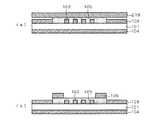
図1は、第1実施形態に係る弾性表面波装置の製造方法を説明する図である。図1(a)〜図1(d)は、弾性表面波装置1の仕掛品の断面図、図1(e)は、弾性表面波装置1の断面図となっている。図1(a)〜図1(e)は、弾性表面波装置1の仕掛品又は弾性表面波装置1の各部の位置関係の理解を助けるための模式図である。 Drawing 1 is a figure explaining the manufacturing method of the surface acoustic wave device concerning a 1st embodiment. 1A to 1D are cross-sectional views of the work in progress of the surface acoustic wave device 1, and FIG. 1E is a cross-sectional view of the surface acoustic wave device 1. FIG. 1A to FIG. 1E are schematic views for assisting in understanding the in-process product of the surface acoustic wave device 1 or the positional relationship of each part of the surface acoustic wave device 1.
図1(e)に示すように、第1実施形態に係る弾性表面波装置の製造方法により製造される弾性表面波装置1は、圧電基板101と、圧電基板101の一の主面たる上面に形成されたIDT(InterDigital Transducer)電極102及び接続線103と、圧電基板101の他の主面たる下面に形成された裏面電極104と、圧電基板101の上面に形成されIDT電極102を覆う保護膜105と、保護膜105の上面に形成されIDT電極102が形成された領域191を囲む枠体106と、枠体106の上面に載置され領域191を覆う蓋体107とを備える。枠体106と蓋体107とは、接合されて、保護カバー117となっている。 As shown in FIG. 1E, the surface acoustic wave device 1 manufactured by the method for manufacturing the surface acoustic wave device according to the first embodiment includes a
弾性表面波装置1は、フィルタ、共振子、遅延線、トラップ等のいずれであってもよい。また、IDT電極102が励振する弾性波は、レイリー波、SH波のいずれであってもよい。さらに、弾性表面波装置1がフィルタである場合は、弾性波表面波装置1は、共振器型フィルタ、トランスバーサル型フィルタのいずれであってもよい。 The surface acoustic wave device 1 may be any of a filter, a resonator, a delay line, a trap, and the like. Further, the elastic wave excited by the
続いて、第1実施形態に係る弾性表面波装置の製造方法を順を追って説明する。 Next, a method for manufacturing the surface acoustic wave device according to the first embodiment will be described in order.
{IDT電極形成工程}
弾性表面波装置1の製造にあたっては、まず、図1(a)に示すように、圧電基板101の上面の弾性表面波素子領域192にIDT電極102及び接続線103を形成し、圧電基板101の下面の全面に裏面電極104を形成する。ここで、「弾性表面波素子領域」とは、1個の弾性表面波装置1を構成するのに必要なIDT電極102及び接続線103が含まれる領域を意味する。{IDT electrode formation process}
In manufacturing the surface acoustic wave device 1, first, as shown in FIG. 1A, the
圧電基板101は、圧電材料の基板である。圧電材料としては、例えば、タンタル酸リチウム(LiTaO3)、ニオブ酸リチウム(LiNbO3)、水晶(SiO2)、四ホウ酸リチウム(Li2B4O7)、酸化亜鉛(ZnO)、ニオブ酸カリウム(KNbO3)、ランガサイト(La3Ga3SiO14)等の単結晶を用いることができる。The
IDT電極102は、導電材料の膜である。導電材料としては、例えば、アルミニウム−銅(Al−Cu)合金に代表されるアルミニウム(Al)合金、アルミニウム(Al)単体金属等を用いることができる。なお、IDT電極102は、異種の導電材料からなる複数の層を積層した膜であってもよい。 The
IDT電極102の平面形状は、少なくとも一対の櫛歯状電極121,122(図2参照)を電極指が交互に配列されるように互いに噛み合わせた平面形状となっている。IDT電極102は、一対の櫛歯状電極121,122に印加された励振信号に応じた弾性表面波を圧電基板101の上面に励振する励振電極として機能する。 The planar shape of the
なお、単数個のIDT電極102で弾性表面波装置1を構成することは必須ではなく、複数個のIDT電極102を直列接続や並列接続等の接続方式で接続して弾性表面波装置1を構成してもよい。このように複数個のIDT電極102を接続すれば、ラダー型弾性表面波フィルタ、ラティス型弾性表面波フィルタ、2重モード弾性表面波フィルタ等を構成することができる。 The surface acoustic wave device 1 is not necessarily composed of a
接続線103も、導電材料の膜である。導電材料としては、例えば、アルミニウム−銅合金に代表されるアルミニウム合金、アルミニウム単体金属等を用いることができる。なお、接続線103も、異種の導電材料からなる複数個の層を積層した膜であってもよい。 The
接続線103は、IDT電極102と接続されている。接続線103は、IDT電極102と外部回路とを接続するために設けられている。 The
接続線103の線幅は、特に制限されないが、IDT電極102と接続されていない側の端部を幅広とすることが望ましい。幅広とすれば、外部回路との接続が容易になるからである。 The line width of the
IDT電極102及び接続線103は、スパッタリング法、蒸着法、CVD(Chemical Vapor Deposition)法等の薄膜形成法により形成した膜を、縮小投影露光機(ステッパー)とRIE(Reactive Ion Etching)装置とを用いたフォトリソグラフィ法等によりパターニングして所望の形状に加工することにより得ることができる。なお、この方法によりIDT電極102及び接続線103を形成する場合、IDT電極102及び接続線103を同一材料で構成して同一工程において形成することが望ましい。 The
裏面電極104も、導電材料の膜である。導電材料としては、例えば、アルミニウム−銅合金に代表されるアルミニウム合金、アルミニウム単体金属等を用いることができる。なお、裏面電極104もは、異種の導電材料からなる複数個の層を積層した膜であってもよい。 The
裏面電極104も、スパッタリング法、蒸着法、CVD法等の薄膜形成法により形成することができる。裏面電極104は、必ずしも必須ではない。ただし、裏面電極104を設ければ、温度変化により圧電基板101の表面に誘起された焦電電荷を接地により解消することができるので、スパーク等による圧電基板101の割れやIDT電極102の電極指間及び複数のIDT電極102の間のスパークの問題を低減させることができる。 The
なお、弾性表面波を閉じ込めるために、圧電基板101の上面に反射器電極を形成してもよい。このような反射器電極は、IDT電極102から見て弾性表面波の2つの伝播方向に形成される。反射器電極を形成する場合、反射器電極及びIDT電極102を同一材料で構成して同一工程において形成することが望ましい。 A reflector electrode may be formed on the upper surface of the
{保護膜形成工程}
次に、図1(b)に示すように、IDT電極102の全部及び接続線103の一部を覆う保護膜105を形成する。{Protective film formation process}
Next, as shown in FIG. 1B, a
保護膜105は、絶縁材料の膜である。絶縁材料としては、例えば、酸化ケイ素(SiO2)、窒化ケイ素(Si3N4)、シリコン(Si)等を用いることができる。The
保護膜105は、CVD法、スパッタリング法等の薄膜形成法により形成した膜の一部をフォトリソグラフィ法により除去することにより得ることができる。ここで、一部を除去するのは、接続線103の一部を露出させ、弾性表面波装置1を外部回路と接続することができるようにするためである。 The
保護膜105は、IDT電極102及び接続線103を保護し、IDT電極102及び接続線103の酸化を低減する。 The
{枠体形成工程}
次に、図1(c)に示すように、弾性表面波素子領域192の上に、IDT電極102が形成された領域191を囲む枠体106を形成する。枠体106は、少なくともIDT電極102を囲うように形成すればよいが、IDT電極102の他に接続線103や反射器電極等を含む領域を囲うように形成してもよい。{Frame body forming process}
Next, as shown in FIG. 1C, a
枠体106は、通常の膜形成方法により圧電基板101の上に形成した膜をパターニングすることにより形成してもよいし、別体の枠状体を圧電基板101の上に貼り合わせることにより形成してもよい。 The
前者の方法により枠体106を形成する場合、例えば、第1レジストからなる第1レジスト膜をフォトリソグラフィ法によりパターニングした後に硬化させることにより枠体106を形成することができる。この場合、第1レジストとしては、例えば、エポキシ系樹脂、ポリイミド系樹脂、BCB(ベンゾシクロブテン)系樹脂、アクリル系樹脂等の樹脂を用いることができる。第1レジストからなる膜は、例えば、弾性表面波素子領域192の上にスピンコート法、印刷法等によりレジスト液を塗布することにより形成することができる。中でも、スピンコート法により第1レジストからなる膜を形成することが望ましい。スピンコート法により第1レジストからなる膜を形成した場合、下地となる構造に多少の段差があっても、下地となる構造との間に隙間を作ることなく第1レジストからなる膜を形成することができ、密着性に優れた枠体106を形成することができるからである。このようにして形成された第1レジストからなる膜は、露光工程及び現像工程を経て、IDT電極102が形成された領域191を囲む枠体106に加工される。 When forming the
{蓋体形成工程}
次に、枠体106の上面にフィルム状の蓋体107を載置して、枠体106と蓋体107とを接合する。これにより、IDT電極102が形成された領域191との間に密閉された振動空間(密閉空間)193を設ける保護カバー117を形成することができる。{Lid formation process}
Next, a film-
蓋体107は、フィルム状の膜を枠体106上に載置してから通常のフォトリソグラフィ技術によりパターニングすることにより形成してもよいし、別体のパターニング加工後の蓋状体を枠体106の上面に載置することにより形成してもよい。ここで、フィルム状とは、感光性を有する材料を含む場合に、膜の厚み方向からの光照射に対して厚み方向全体で反応が進む程度に薄いものとする。なお、以下では、第2レジストからなるフィルム状の成形体である第2フィルム115を載置してからパターニングすることで蓋体107を形成する例について説明する。 The
第2フィルム115を用いて蓋体107を形成する場合、まず、図1(d)に示すように、第2フィルム115を枠体106の上面に載置してIDT電極102が形成された領域191を覆う。第2レジストとしては、例えば、エポキシ系樹脂、ポリイミド系樹脂、BCB系樹脂、アクリル系樹脂等の樹脂を用いることができる。第2フィルム115は、予めフィルム状に成形されているので、枠体106の上面に載置するだけで圧電基板101との間に振動空間193を形成することができる。第2フィルム115を枠体106の上面に載置するためには、温度管理をしながらローラーでフィルムを加圧して貼り付けることのできる貼り付け機を用いて、温度及び圧力を適宜設定し、第2フィルム115を枠体106の上面に貼り付ければよい。 When the
次に、図1(e)に示すように、露光工程及び現像工程を経て、載置された第2フィルム115の枠体106よりも外側の部分を除去し、IDT電極102が形成された領域191を覆う蓋体107に加工する。その後に、枠体106と蓋体107とを接合し、保護カバー117を形成する。枠体106と蓋体107とを接合するためには、レジスト材料に応じて、枠体106及び蓋体107を加熱したり、枠体106及び蓋体107に光を照射したりすればよい。例えば、枠体106及び蓋体107の材料としてエポキシ樹脂を用いた場合であれば、枠体106及び蓋体107を100℃程度に加熱すればよい。このように形成された保護カバー117により、振動空間193を設けることができるとともに、IDT電極102を封止することができるので、IDT電極102等の酸化等を低減することができる。 Next, as shown in FIG. 1 (e), an area where the
なお、このようにして枠体106形成後に蓋体107を形成し、両者を接合した場合には、枠体106の断面形状が台形状になることが多い。枠体106をパターニングした直後には断面形状が直方形であったとしても、その上に蓋体107を設け、両者を接合するために一旦熱等が加えられることにより変形するためである。 When the
{弾性表面波装置の信頼性}
このようなIDT電極形成工程、保護膜形成工程、枠体形成工程及び蓋体形成工程を経て、図1(e)に示す弾性表面波装置1を製造することができる。第1実施形態に係る弾性表面波装置の製造方法によれば、振動空間193を形成するために犠牲層を用いる必要がないので、犠牲層を用いた場合のように犠牲層を除去する際にエッチャントやエッチングによる残留生成物が形成した中空構造の内部(振動空間193)に残ることがない。したがって、第1実施形態に係る弾性表面波装置の製造方法によれば、製造した弾性表面波装置1の電気特性が劣化することを低減することができる。すなわち、製造した弾性表面波装置1の信頼性を向上することができる。{Reliability of surface acoustic wave devices}
The surface acoustic wave device 1 shown in FIG. 1E can be manufactured through such an IDT electrode forming step, a protective film forming step, a frame forming step, and a lid forming step. According to the method for manufacturing the surface acoustic wave device according to the first embodiment, it is not necessary to use a sacrificial layer to form the
{外部回路との接続}
弾性表面波装置1を外部回路と接続するためには、図1(e)に示すように、接続線103を保護カバー117の外側に引き出し、保護カバー117の外側において、接続線103の上に外部接続用の電極を形成したり、接続線103に外部接続用のワイヤをボンディングしたりすればよい。{Connection with external circuit}
In order to connect the surface acoustic wave device 1 to an external circuit, as shown in FIG. 1 (e), the
このように接続線103の一部を保護カバー117すなわち枠体106の外側に引き出すように延在させている場合には、振動空間193を封止した状態で、外部回路にあわせて接続線103の位置を自由に決定することができる。このため、汎用性の高い弾性表面波装置1を製造することができる。ただし、接続線103を保護カバー117の外側に引き出すことは必須ではない。例えば、保護カバー117で覆われた内側において圧電基板101にビアホールを形成して圧電基板101の下面で外部回路と接続することができるようにしてもよいし、保護カバー117の枠体106の部分とその上に位置する蓋体107の一部とに貫通穴を設けて保護カバー117の上面で外部回路と接続することができるようにしてもよい。 When a part of the
{保護膜の上面への枠体の形成}
図2は、弾性表面波装置1の平面透視図である。先述の図1(e)は、図2のA−Aの切断線における弾性表面波装置1の断面図となっている。図2においては、枠体106の配置を分かり易くするために、枠体106の部分にハッチングを付している。図2に示すように、保護膜105は、IDT電極102及び接続線103が形成された領域の一部に形成されている。{Formation of frame on upper surface of protective film}
FIG. 2 is a plan perspective view of the surface acoustic wave device 1. FIG. 1E is a cross-sectional view of the surface acoustic wave device 1 taken along the line AA in FIG. In FIG. 2, the
枠体106は、IDT電極102を覆う保護膜105の上面に形成することが望ましい。理由は明らかではないが、保護膜105の上面に枠体106を形成すると、枠体106の被形成面(ここでは、保護膜105の上面)への密着性を向上することができるからである。例えば、保護膜105の材料として酸化ケイ素と用いて、第1レジストとしてエポキシ系樹脂を用いた場合には、枠体106の被形成面への密着性を向上することができる。これは、酸化ケイ素とエポキシ系樹脂との間の水素結合によるものと推察される。 The
また、接続線103を保護カバー117の外側に引き出した場合、枠体106が接続線103を跨ぐことになるが、保護膜105の上面に枠体106を形成すれば、接続線103により生じる段差を保護膜105が緩和するので、ほぼ平坦な被形成面に枠体106を形成することができる。このため、接続線103を保護カバー117の外側に引き出した場合、枠体106を保護膜105の上面以外に形成するよりも枠体106を保護膜105の上面に形成する方が、枠体106を被形成面に強固に接続することができる。 Further, when the
ただし、これらのことは、枠体106を保護膜105の上面以外に形成することを妨げるものではない。 However, these do not preclude the formation of the
{第1レジスト及び第2レジストの選択}
枠体形成工程及び蓋体形成工程において、第1レジストと第2レジストとを同一材料とすれば、枠体106と蓋体107とを接合した場合に両者を一体化することができる。また、第1レジストと第2レジストとを同一材料とすれば、両者の接合界面が同一材料同士の界面となるので、両者の密着強度や保護カバー117の気密性を向上することができる。したがって、高信頼性の弾性表面波装置1を製造することができる。特に、第1レジスト及び第2レジストとしてエポキシ系樹脂を用いて、枠体106及び蓋体107を100℃から200℃までの範囲で加熱した場合には、より重合が促進されるため、両者の密着強度や保護カバー117の気密性を向上することができる。{Selection of first resist and second resist}
If the first resist and the second resist are made of the same material in the frame body forming step and the lid body forming step, they can be integrated when the
また、第1レジストと第2レジストとを同一材料とすれば、これらにより形成される枠体106と蓋体107とが同一材質となり、その結果、保護カバー117を一体化することができる。 Further, if the first resist and the second resist are made of the same material, the
<第2実施形態>
第2実施形態は、第1実施形態に係る弾性表面波装置の製造方法の枠体形成工程に代えて採用することができる枠体形成工程に関する。Second Embodiment
The second embodiment relates to a frame forming process that can be employed in place of the frame forming process of the method for manufacturing the surface acoustic wave device according to the first embodiment.
図3は、第2実施形態に係る枠体形成工程を説明する図である。図3(a)及び図3(b)は、弾性表面波装置1の仕掛品の断面図となっている。図3(a)及び図3(b)は、弾性表面波装置1の仕掛品の各部の位置関係の理解を助けるための模式図である。 FIG. 3 is a view for explaining a frame forming process according to the second embodiment. 3A and 3B are cross-sectional views of the work in progress of the surface acoustic wave device 1. FIG. 3A and FIG. 3B are schematic views for helping understanding of the positional relationship of each part of the work in progress of the surface acoustic wave device 1.
第2実施形態に係る枠体形成工程においては、第1レジストからなる膜としてフィルム状の成形体を用いる。すなわち、まず、図3(a)に示すように、第1レジストからなる第1フィルム219を圧電基板101の上に載置する。その後で、図3(b)に示すように、フォトリソグラフィ法により第1フィルム219をパターニングした後に硬化させる。 In the frame forming process according to the second embodiment, a film-like molded body is used as the film made of the first resist. That is, first, as shown in FIG. 3A, the
第2実施形態に係る枠体形成工程によれば、均一な厚さの枠体106を形成することができるので、第2フィルム115を枠体106の上面に隙間なく載置することができる。このため、簡易な工程で確実に弾性表面波素子領域192の上の振動空間193を封止することができる。 According to the frame body forming step according to the second embodiment, the
また、第2実施形態に係る枠体形成工程によれば、フォトリソグラフィ法により第1フィルム219をパターニングすることができるので、所望の場所に精度良く数マイクロメートル程度の微細なパターンを形成することができる。このため、枠体106を所望のパターンに精度良く形成することができる。 Further, according to the frame forming process according to the second embodiment, the
<第3実施形態>
第3実施形態は、第1実施形態に係る弾性表面波装置の製造方法の蓋体形成工程に代えて採用することができる蓋体形成工程に関する。<Third Embodiment>
The third embodiment relates to a lid forming process that can be employed instead of the lid forming process of the method for manufacturing the surface acoustic wave device according to the first embodiment.
図4(a)〜図4(d)は、第3実施形態に係る蓋体形成工程を説明する図である。図4(a)〜図4(c)は、弾性表面波装置1の仕掛品の断面図、図4(d)は、弾性表面波装置1の断面図となっている。図4(a)〜図4(d)は、弾性表面波装置1の仕掛品又は弾性表面波装置1の各部の位置関係の理解を助けるための模式図である。 FIG. 4A to FIG. 4D are diagrams for explaining a lid forming process according to the third embodiment. 4A to 4C are cross-sectional views of the work in progress of the surface acoustic wave device 1, and FIG. 4D is a cross-sectional view of the surface acoustic wave device 1. FIG. 4A to FIG. 4D are schematic diagrams for assisting in understanding the work relationship of the surface acoustic wave device 1 or the positional relationship of each part of the surface acoustic wave device 1.
図4(a)に示すように、第3実施形態に係る蓋体形成工程において使用される第2フィルム315は、樹脂層315aと、樹脂層315aに比べヤング率の高い保持層315bとの2層を積層して構成されている。 As shown in FIG. 4 (a), the
具体的には、樹脂層315aとしては、感光性を有し、熱により硬化しかつ機械強度及び耐薬品性に優れるものが好ましい。例えば、エポキシ系樹脂、ポリイミド系樹脂、BCB系樹脂、アクリル系樹脂等からなる層を用いることができる。保持層315bとしては、PET(PolyEthylene Terephthalate)フィルム等、樹脂層315aに比べヤング率が高いとともに、樹脂層315aからの剥がれ性が良好でかつ熱的に安定である材料を用いる。なお、保持層315bは、透光性を有するものとする。保持層315bを通して樹脂層315aを露光するためである。また、保持層315bは、樹脂層315aを硬化させる温度においても変質しない耐熱性を有することが求められる。 Specifically, the
なお、樹脂層315a及び保持層315bのヤング率は、例えば、ISO規格(例えばISO14577)に準拠するような条件でナノインデンテーション法のような、薄膜のヤング率を測定する方法で測定すればよい。 Note that the Young's modulus of the
このような工程で形成した保護カバー117の上面、すなわち、蓋体107の上面は、下面に比べて表面粗さが大きくなっている。樹脂層315aを硬化させた後に保持層315bを剥離するためである。 The upper surface of the
第3実施形態に係る蓋体形成工程においては、まず、図4(a)に示すように、第2フィルム315を枠体106の上面に保持層315bが上側となるように、すなわち、樹脂層315aが枠体106と接するように載置する。 In the lid forming step according to the third embodiment, first, as shown in FIG. 4A, the
次に、図4(b)に示すように、第2フィルム315をフォトリソグラフィ法によりパターニングする。すなわち、保持層315bの上から第2フィルム315をマスク(不図示)を用いて露光した後に加熱して、樹脂層315aを露光部315cと未露光部315dとする。ここで、露光部315cは、露光後の加熱により硬化されて蓋体107となり、それと同時に枠体106と接合される。 Next, as shown in FIG. 4B, the
次に、図4(c)に示すように、第2フィルム315の保持層315bを除去する。 Next, as shown in FIG. 4C, the
次に、図4(d)に示すように、現像工程により、枠体106の外側に位置する樹脂層315a(この例では未露光部315d)を除去して分離された蓋体107とした後に、さらに加熱する。これにより、蓋体107が完全に硬化させられるとともに、枠体106と蓋体107とが完全に一体化され、保護カバー117が得られる。 Next, as shown in FIG. 4D, after the development process, the
なお、保持層315bを現像後に除去してもよい。 Note that the
第3実施形態の蓋体形成方法によれば、枠体106の上面に均一に第2フィルム315を貼り合わせて接合することができる。また、第2フィルム315の硬化前であっても、ヤング率の高い保持層315bが第2フィルム315の全体の変形を抑制するので、IDT電極102との間に振動空間193を保つことができる。このため、第2フィルム315の載置、露光、加熱の間に振動空間193が潰れることなく、確実に振動空間193を形成することができる。また、保持層315bが樹脂層315aを保持することにより、第2フィルム315の取り扱いが容易になる。 According to the lid forming method of the third embodiment, the
また、第3実施形態に係る蓋体形成工程によれば、フォトリソグラフィ法により第2フィルム315をパターニングすることができるので、所望の場所に精度良く数マイクロメートル程度の微細なパターンを形成することができる。このため、蓋体307を所望のパターンに精度良く形成することができる。 In addition, according to the lid forming process according to the third embodiment, the
<第4実施形態>
第4実施形態は、第1実施形態に係る弾性表面波装置の製造方法のIDT電極形成工程、保護膜形成工程、枠体形成工程及び蓋体形成工程に続いて行う、電極形成方法に関する。<Fourth embodiment>
The fourth embodiment relates to an electrode forming method performed subsequent to the IDT electrode forming step, the protective film forming step, the frame forming step, and the lid forming step of the method for manufacturing the surface acoustic wave device according to the first embodiment.
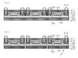
図5(a)〜図5(h)は、第4実施形態に係る電極形成方法を説明する図である。図5(a)〜図5(g)は、弾性表面波装置4の仕掛品の断面図、図5(h)は、弾性表面波装置4の断面図となっている。なお、図5(a)〜図5(h)においては、図1(a)〜図1(e)に図示した構成要素と同様の構成要素には同じ参照符号を付している。 Fig.5 (a)-FIG.5 (h) are the figures explaining the electrode formation method which concerns on 4th Embodiment. 5A to 5G are cross-sectional views of the work in progress of the surface acoustic wave device 4, and FIG. 5H is a cross-sectional view of the surface acoustic wave device 4. In FIG. 5A to FIG. 5H, the same reference numerals are given to the same components as those shown in FIG. 1A to FIG.
図5(h)に示すように、第4実施形態に係る電極形成方法により外部回路と接続するための電極を形成した弾性表面波装置4は、1枚のウエハ状の圧電基板101、IDT電極102、接続線103、裏面電極104、保護膜105、枠体106及び蓋体107に加えて、メッキ用下地層408の残存部408a、柱状電極410、封止樹脂膜411、保護層412及び外部接続電極413を備える。 As shown in FIG. 5 (h), the surface acoustic wave device 4 in which electrodes for connecting to an external circuit are formed by the electrode forming method according to the fourth embodiment includes a single wafer-like
続いて、第4実施形態に係る電極形成方法を順を追って説明する。 Subsequently, an electrode forming method according to the fourth embodiment will be described in order.
{メッキ用下地層形成工程}
外部回路と接続するための電極を形成するのにあたっては、まず、図5(a)に示すように、図1(e)に示す状態から、保護カバー117が形成された圧電基板101の上の弾性表面波素子領域192を覆うメッキ用下地層408を形成する。{Plating underlayer forming process}
In forming an electrode for connecting to an external circuit, first, as shown in FIG. 5A, from the state shown in FIG. 1E, on the
メッキ用下地層408は、後述する柱状電極410を構成する金属を電気的又は化学的に析出させるために形成される。このため、メッキ用下地層408には、柱状電極410と同一材料を使用することが望ましい。なお、一般的には、銅(Cu)が用いられる。メッキ用下地層408に銅を用いた場合、接続線103を形成するアルミニウム−銅(Al−Cu)合金との密着性を考慮すると、クロム(Cr)やチタン(Ti)からなる密着層をアルミニウム−銅合金からなる接続線103とメッキ用下地層408との間に介在させることが望ましい。 The
メッキ用下地層408は、100nm以上の厚さに形成することが望ましい。これは、柱状電極410を電気メッキ法で形成するときに、安定して電流を流すために必要な厚さである。 The
メッキ用下地層408は、柱状電極410を形成する領域を含む圧電基板101の全面に、例えば、チタン−銅(Ti−Cu)等を用いて形成する。このようなメッキ用下地層408を形成することにより、メッキ用下地層408を介して、電気メッキ法によって銅等の金属を厚く形成することができる。 The
メッキ用下地層408を形成する方法は制限されないが、メッキ用下地層408をフラッシュメッキ法により形成する場合には、メッキを形成すべき部分に電流を流すための配線パターンを形成する必要がないため、弾性表面波装置4の小型化が可能となる。一方、フラッシュメッキ法により保護カバー117を含む構造体の全面の上にメッキ用下地層408を形成する場合には、メッキが形成されない部分が段差の部分に生じる可能性がある。これは、フラッシュメッキ法により形成されるメッキ下地層408は、非常に薄いため、大きな段差の部分においてステップカバレッジが充分でないからである。このことから、図5(a)に示すように、保護カバー117を除く部分にメッキ下地層408が形成されない部分が生じるような大きな段差がないようにすることが望ましい。具体的には、保護カバー117を除く部分の段差は、メッキ用下地層408の厚さの半分以下の段差とすることが好ましい。例えば、メッキ用下地層408の厚さが0.7μmであるときは、段差を0.35μm以下とすればよい。これにより、たとえ、保護カバー117の部分の段差(例えば、保護カバー117の側面部195)にメッキが形成されない部分があり、蓋体107の上面と接続線103が形成されている面との導通がとれなくても、柱上電極410を形成する接続線103が形成されている面の上のメッキ用下地層408は確実に電気的につながっている。このため、電気メッキ法で柱状電極410を形成する際に、メッキ用下地層408に確実に電流を流すことができる。 The method for forming the
{メッキ用レジスト膜形成工程}
次に、図5(b)に示すように、保護カバー117の外側に位置する接続線103の上に開口部416を有するメッキ用レジスト膜409をメッキ用下地層408の上に形成する。{Plating resist film forming process}
Next, as shown in FIG. 5B, a plating resist
メッキ用レジスト膜409は、例えば、スピンコート等の手法でメッキ用下地層408の上に形成される。なお、使用するレジスト液の粘度やスピンコートによる塗布回数により、メッキ用レジスト膜409の厚さを数μmから数100μmまでの間でコントロールすることが可能である。また、メッキ用レジスト膜409の開口部416は、一般的なフォトリソグラフィ法により形成することが望ましい。 The plating resist
{柱上電極形成工程}
次に、図5(c)に示すように、開口部416の底に露出するメッキ用下地層408の上に、メッキ法により柱状電極410を形成する。{Column electrode formation process}
Next, as shown in FIG. 5C, the
柱状電極410は、電気メッキ法、無電解メッキ法、スタッドバンプ法等により形成することができるが、電気メッキ法により形成することが好適である。電気メッキ法によれば、メッキ膜の成長速度が速くメッキ膜を厚く形成しやすいことから、柱状電極410の高さの自由度を高めることができるからである。また、電気メッキ法によれば、メッキ下地層408との密着性が良好なものとなるからである。なお、メッキ膜の厚さはメッキ処理時間で決定されるが、30μmを超える厚さのメッキ膜を形成する場合には、成長速度が速い電気メッキ法により形成することが好ましい。 The
柱状電極410の材料としては、例えば、半田、銅(Cu)、金(Au)、ニッケル(Ni)を用いることができる。特に、柱状電極410の材料として半田や銅を用いた場合には、メッキの材料費を低減することができるため、弾性表面波装置4を安価にすることができる。 As a material of the
{除去工程}
次に、図5(d)に示すように、柱状電極410を残し、メッキ用レジスト膜409とメッキ用下地層408とを除去する。{Removal process}
Next, as shown in FIG. 5D, the
メッキ用レジスト膜409は、アセトンやイソプロピルアルコール(IPA)等の有機溶剤やジメチルスルフォキシド等のアルカリ性有機溶剤で除去することができる。 The plating resist
メッキ用下地層408は、例えば、銅からなる場合には、塩化第2鉄の水溶液や燐酸と過酸化水素水との混合液で除去することができる。一方、メッキ用下地層408は、例えば、チタンからなる場合には、希フッ酸の水溶液やアンモニアと過酸化水素水との混合液で除去することができる。中でも、メッキ用下地層408の下に形成されている酸化ケイ素(SiO2)膜やアルミニウム−銅合金等からなる接続線103へのダメージを少なくするためには、アンモニアと過酸化水素水との混合液で除去することが望ましい。For example, when the
なお、上述のようにメッキ用レジスト膜409を除去して柱状電極410を露出させた後にメッキ用下地層408を除去しても、メッキ下地層408は薄いので、柱状電極410の下に位置するメッキ用下地層408は、外縁部が一部除去されるが、それ以外の残存部408aは残る。したがって、柱状電極410を残すことができる。 Even if the
{封止樹脂膜形成工程}
次に、図5(e)に示すように、圧電基板1の弾性表面波素子領域192の上に、保護カバー117と柱状電極410とを覆う封止樹脂膜411を形成する。{Sealing resin film forming step}
Next, as illustrated in FIG. 5E, a sealing
封止樹脂膜411の材料としては、フィラーを混入させることにより熱膨張係数を圧電基板101とほぼ等しくなるように調整することができ、耐薬品性にも優れたエポキシ系樹脂が好適である。特に、線膨張係数が圧電基板101に近いエポキシ系樹脂を使用したり、弾性率が低いエポキシ系樹脂を使用したりして、圧電基板101に加わる応力を少なくすることが望ましい。 As a material of the sealing
また、封止樹脂膜411に気泡が混入すると安定して保護カバー117を含む構造体を封止することができないので、真空印刷法により封止樹脂膜411を印刷することも好ましい。 Moreover, since a structure including the
なお、封止樹脂膜411の厚さは、柱状電極410が覆われる程度が望ましい。 Note that the thickness of the sealing
{柱状電極露出工程}
次に、図5(f)に示すように、封止樹脂膜411の上面を研磨して、柱状電極410を露出させる。{Columnar electrode exposure process}
Next, as shown in FIG. 5F, the upper surface of the sealing
具体的には、封止樹脂膜411の上面を、グラインダーにより研磨刃を用いて柱状電極410が露出するまで研磨する。後述する外部接続電極413と柱状電極410とを良好に接続するために、バフ研磨等により仕上げ加工を加えても良い。 Specifically, the upper surface of the sealing
{外部接続電極形成工程}
次に、図5(h)に示すように、柱状電極410の上面に外部接続電極413を形成する。{External connection electrode formation process}
Next, as illustrated in FIG. 5H, the
外部接続電極413は、鉛スズ(PbSn)半田、鉛(Pb)フリー半田、金スズ(AuSn)半田、金ゲルマニウム(AuGe)半田等の半田を用いて形成したバンプであってもよいし、導電材料で薄膜を形成することにより形成したフラットなパットであってもよい。例えば、クリーム半田を柱状電極410の上部にスクリーン印刷してリフローすることにより外部接続電極413を形成することができる。 The
{弾性表面波装置の実装}
このようなメッキ用下地層形成工程、メッキ用レジスト膜形成工程、柱状電極形成工程、除去工程、封止樹脂膜形成工程、柱状電極露出工程、外部接続電極形成工程を経ることで、表面実装可能な弾性表面波装置4を提供することができる。さらに、封止樹脂411の上面に露出する柱状電極410の上に外部接続電極413を形成することで、さらに実装の容易な弾性表面波装置とすることができる。{Implementation of surface acoustic wave device}
Surface mounting is possible through such a plating underlayer formation process, plating resist film formation process, columnar electrode formation process, removal process, sealing resin film formation process, columnar electrode exposure process, and external connection electrode formation process. A surface acoustic wave device 4 can be provided. Furthermore, by forming the
第4実施形態に係る電極形成方法によれば、弾性表面波装置4をウエハレベルで製造することができるので、複雑な工程を経ることなく弾性表面波装置4を提供することができる。また、第4実施形態に係る電極形成方法によれば、弾性表面波装置4を実装する実装基板に応じて外部接続電極413を形成する材料を選択することができるので、弾性表面波装置4と実装基板との接合信頼性を向上することができる。 According to the electrode forming method according to the fourth embodiment, since the surface acoustic wave device 4 can be manufactured at the wafer level, the surface acoustic wave device 4 can be provided without going through complicated steps. In addition, according to the electrode forming method according to the fourth embodiment, the material for forming the
加えて、第4実施形態に係る電極形成方法を用いて製造した弾性表面波装置4を分波器に使用した場合、柱状電極410を放熱用電極としても用いることができる。したがって、IDT電極102における発熱箇所の近傍に柱状電極410を配置することにより、放熱性に優れた弾性表面波装置4を提供することができる。IDT電極102における発熱箇所は、使用周波数、IDT電極102が複数個ある場合にはその接続方法によっても異なるが、弾性表面波装置4が共振子の場合にはIDT電極102の中心部分付近となる。また、この柱状電極410の配置、本数、径を工夫することで、放熱性を向上することができる。 In addition, when the surface acoustic wave device 4 manufactured using the electrode forming method according to the fourth embodiment is used for a duplexer, the
{保護層形成工程}
弾性表面波装置4の製造において、圧電基板101の下面に、封止樹脂膜411と熱膨張係数が略同一の材料からなる保護層412を形成する工程をさらに設けてもよい。なお、図5(a)〜図5(h)は、柱状電極露出工程と外部接続用電極形成工程との間にこのような保護層形成工程を設けた場合の電極形成方法を示している。{Protective layer forming step}
In the production of the surface acoustic wave device 4, a step of forming a
このような保護層形成工程により、IDT電極102が形成されていない圧電基板101の下面が保護層412で保護された構造となるので、製造時及び製造後における弾性表面波装置4の耐衝撃性を向上することができる。そのため、弾性表面波装置4の割れ、カケ等の不良を発生を抑制し、歩留まりを向上し、弾性表面波装置4の信頼性を向上することができる。 Since the lower surface of the
なお、保護層412を圧電基板101の下面から側面にかけて形成した場合には、圧電基板101の下面及び側面が保護された構造となるので、圧電基板101と封止樹脂411との界面から水分が浸入することを抑制し、気密性、耐湿性を向上させた弾性表面波装置4を実現することができる。 In the case where the
また、封止樹脂膜411と熱膨張係数が略同一の材料を圧電基板101の下面の保護層412に用いるため、製造工程における封止樹脂膜411による応力を緩和することができ、圧電基板101に反りを発生させることなく、弾性表面波装置4の信頼性を向上させることができる。 In addition, since a material having substantially the same thermal expansion coefficient as that of the sealing
なお、このような保護層形成工程は、上述のIDT電極形成工程の前から外部接続電極形成工程の後の間に適宜追加すればよいが、圧電基板101の上面に封止樹脂膜411を形成する封止樹脂膜形成工程以降に設ければ、圧電基板101と封止樹脂膜411との間の熱膨張係数の違いにより圧電基板101に加わる応力を圧電基板101の上面と下面とで打ち消すことができる。特に、図5(g)に示すように、保護層形成工程を柱上電極露出工程と外部接続電極形成工程との間に設けると、圧電基板101の反りに起因するプロセスの不具合や圧電基板101にかかるストレス(応力)を低減することができ、弾性表面波装置4の信頼性を向上することができる。 Note that such a protective layer forming step may be added as appropriate before the above-described IDT electrode forming step and after the external connection electrode forming step, but the sealing
保護層412の材料は、封止樹脂膜411と熱膨張係数が略同一であれば限定されないが、エポキシ系樹脂とすることが好適である。エポキシ系樹脂とすれば、酸化ケイ素(SiO2)等のフィラーを添加することにより熱膨張係数をコントロールすることができるため、圧電基板101に加わる応力を圧電基板101の上面と下面とで打ち消すことができるからである。また、エポキシ系樹脂とすれば、透湿性が低く、かつ、吸水性が高いため、弾性表面波装置4への水分の浸入を抑制することができるからである。The material of the
{柱状電極の高さ}
柱状電極形成工程においては、図5(d)に示すように、柱状電極410を保護カバー117よりも高くなるように形成し、柱状電極露出工程においては、図5(f)に示すように、保護カバー117が封止樹脂膜411に覆われた状態で封止樹脂膜411の上面に柱状電極410を露出させることが望ましい。このようにすることで、柱状電極露出工程を経た後において、柱状電極410の最上部の高さが、保護カバー117の最上部の高さより高くなるようにすることができるからである。ここで、柱状電極410及び保護カバー117の高さとは、弾性表面波素子領域192からの高さをいう。これにより、柱状電極露出工程で封止樹脂膜411を研磨しても、保護カバー117の蓋体107の部分が露出したり研磨されたりすることがなくなるので、弾性表面波装置4が励振する弾性表面波の振動空間193を確保するための保護カバー117の気密性を十分に確保することができる。{Height of columnar electrode}
In the columnar electrode forming step, as shown in FIG. 5D, the
{メッキ用レジスト膜の形成}
メッキ用レジスト膜形成工程においては、レジスト材料の塗布及び硬化を複数回繰り返すことによりメッキ用レジスト膜409を形成することが望ましい。このように複数回に分けてメッキ用レジスト膜409を形成することにより、被覆性や取り扱い性等に考慮して調整したレジスト材料を用いて、所望の厚さのメッキ用レジスト膜409を形成することができる。また、メッキ用レジスト膜409を所望の厚さに形成することができるようになる結果、所望の高さの柱状電極410を形成することが可能になる。特に、保護カバー117の最上部とほぼ同じ高さになるまでレジスト材料の塗布及び硬化を行い、保護カバー117による大きな段差を埋めて平坦な面を得た後に、所望の厚さを得るようにさらにレジスト材料の塗布及び硬化を繰り返すようにすれば、メッキ用レジスト膜409の上面を平坦にすることができるので好ましい。{Formation of resist film for plating}
In the plating resist film formation step, it is desirable to form the plating resist
<第5実施形態>
第5実施形態は、第1実施形態に係る弾性表面波装置の製造方法及び第2実施形態に係る電極形成方法により製造することができる弾性表面波装置5に関する。<Fifth Embodiment>
The fifth embodiment relates to a surface acoustic wave device 5 that can be manufactured by the method for manufacturing the surface acoustic wave device according to the first embodiment and the electrode forming method according to the second embodiment.
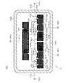
図6は、弾性表面波装置5における複数個のIDT電極520〜525,530、複数個の導体パターン533〜538等の配置を示す平面図である。図6は、弾性表面波装置5の各部の位置関係の理解を助けるための模式図である。また、図6においては、枠体506の部分にハッチングを付している。 FIG. 6 is a plan view showing an arrangement of a plurality of
図6に示すように、弾性表面波装置5は、圧電基板501と、IDT電極520〜525,530と、反射器電極526〜529と、第1導体パターン533,538と、第2導体パターン534〜537と、絶縁層539〜542と、入力端子550と、出力端子551,552と、グランド端子553,554と、接続線571〜575とを備える。 As shown in FIG. 6, the surface acoustic wave device 5 includes a
{弾性表面波素子}
弾性表面波素子領域592には、複数個のIDT電極520〜525,530が形成されている。{Surface acoustic wave element}
A plurality of
3個のIDT電極520〜522及びその両側に配置された2個の反射器電極526,527は、弾性表面波素子531を構成し、3個のIDT電極523〜525及びその両側に配置された2個の反射器電極528,529は、弾性表面波素子532を構成している。 The three
弾性表面波装置5では、圧電基板601の上に、IDT電極530に並列接続された弾性表面波素子531,532を配置する。これらの弾性表面波素子531,532は、縦結合共振器となる。 In the surface acoustic wave device 5, surface
弾性表面波素子531,532は、IDT電極530を介して、不平衡信号が入力される入力端子550に並列に接続されている。入力端子550に接続された左右のIDT電極520,522及び左右のIDT電極523,525は、互いに対向させられた一対の櫛歯状電極の間に電界を印加され、弾性表面波を励振する。このように励振された弾性表面波は、中央のIDT電極521,524にまで伝播させられる。また、中央のIDT電極521における信号の位相は、中央のIDT電極524における信号の位相に対して、180°異なった逆相となっている。したがって、弾性表面波装置5では、最終的に、中央のIDT電極521,524のそれぞれの一方の櫛歯状電極から出力端子551,552へ信号が伝わり、当該信号が平衡信号となり出力される。弾性表面波装置5では、このような構成により、平衡−不平衡変換機能を実現している。 The surface
{端子}
入力端子550、出力端子551,552及びグランド端子553,554の上には、弾性表面波装置4の柱状電極410と同様の柱状電極(不図示)が形成され、外部回路と接続される。{Terminal}
A columnar electrode (not shown) similar to the
{枠体}
枠体506は、IDT電極520〜525,530及び導体パターン533〜538を囲むように配置される。弾性表面波装置4と同様に、枠体506の上面には蓋体(不図示)が載置され、当該蓋体は枠体506と接合されている。枠体506及び当該蓋体は、封止用の保護カバーを形成する。{Frame}
The
{接続線}
接続線571〜575は、枠体506の外側に引き出され、それぞれ、入力端子550、出力端子551,552及びグランド端子553,554に接続されている。接続線571〜573は、入力端子550及び出力端子551,552とIDT電極530,521,524とをそれぞれ接続する。接続線574,575は、第1導体パターン533,538を介してIDT電極520〜525を接地する。{Connection line}
The connection lines 571 to 575 are drawn to the outside of the
接続線571〜575は、IDT電極520〜525,530を外部回路と接続するために、IDT電極520〜525,530に接続されている。接続線571〜575には、(i) 外部回路への接続端子となる入力端子550や出力端子551,552とIDT電極530,521,524とを接続する接続線571〜573のように、IDT電極530,521,524に直接接続された一群だけでなく、(ii) 第1導体パターン533,538を介して外部回路への接続端子となるグランド端子553,554とIDT電極520〜525とを接続する接続線574,575のように、IDT電極520〜525と外部回路とを間接的に接続する一群も含まれる。
{導体パターン}
図6に示すように、弾性表面波素子領域592には、IDT電極520〜525,530に接続された複数個の導体パターン533〜538が形成されている。複数個の導体パターン533〜538は、第1導体パターン533,538と、第1導体パターン533,538と絶縁層539〜542を介して交差する第2導体パターン534〜537とを含む。{Conductor pattern}
As shown in FIG. 6, a plurality of
このように第1導体パターン533,538と第2導体パターン534〜537とを交差させることにより、導体パターン533〜538の配線の自由度を向上することができるので、IDT電極530とIDT電極520〜525との間(段間)を狭め、両者を近接配置することができる。これにより、IDT電極520〜525,530が形成される領域が占める面積を最小化することができ、小型の弾性波表面装置5を実現することができる。 Since the
さらに、第1導体パターン533,538と第2導体パターン534〜547とが交差する導体パターン交差部は、導体である第1導体パターン533,538と第2導体パターン534〜547との間に絶縁層539〜542を介させて構成されている。このため、導体パターン交差部には、第1導体パターン533,538と第2導体パターン534〜547との間に容量を持たせる容量形成部543〜546を設けることができる。容量形成部543〜546は、IDT電極520〜525,530や導体パターン534〜538の配置により寄生容量が発生すると、平衡信号を出力する出力端子551,552に伝わる信号の振幅が互いに異なったり、位相が逆相からずれてしまって平衡度が劣化したりすることがあることを考慮して設けられている。すなわち、IDT電極530と第1及び第2の弾性表面波素子531,532との間に形成された容量形成部543〜546により、寄生容量による影響を打ち消すように、等価回路上導入される容量を弾性表面波素子531,532において調整することが可能となり、振幅平衡度及び位相平衡度を向上することができる。このため、容量形成部543〜546により、弾性表面波装置5の電気特性を向上することができる。また、容量形成部543〜546のキャパシタンスと柱状電極及び導体パターン533〜538によるインダクタンスとを適切に選択することにより、弾性表面波装置5の通過帯域外減衰量を増加させたり、弾性表面波装置5の電気特性を向上したりすることができる。 Furthermore, the conductor pattern intersection where the
さらに、IDT電極520〜525,530同士を接続する導体パターン533〜538の配線を図6のようにすることで、IDT電極520〜525を構成する櫛歯状電極のうち段間側に位置する方を接地する場合でも、当該櫛歯状電極を確実に外部回路との接続のための接続線574,575に接続し、確実に保護カバーの外側に引き出すことができる。このため、複数個のIDT電極520〜525,530を1つの保護カバーで封止しても、外部回路との接続を確保することができるので、個々のIDT電極520〜525,530をそれぞれ保護カバーで覆う場合に比べて弾性表面波素子領域592の面積を大幅に減少させることができる。さらに、振動空間を封止した状態で外部回路との接続を確保することができるので、電気特性が劣化しない弾性表面波装置5を提供することができる。 Furthermore, by arranging the wiring of the
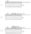
{導体パターンの形成}
図7は、導体パターン533〜538の形成方法を説明する図である。図7(a)及び図7(b)は、形成中の導体パターン交差部の断面図となっており、図7(c)は、形成後の導体パターン交差部の断面図となっている。図7(a)〜図7(c)は、導体パターン交差部の各部の位置関係の理解を助けるための模式図である。{Formation of conductor pattern}
FIG. 7 is a diagram for explaining a method of forming the
導体パターンの形成にあたっては、まず、図7(a)に示すように、IDT電極形成工程において、接続線571〜575を形成する際に同時に、下部に位置する第2導体パターン534〜537を形成する。次に、図7(b)に示すように、弾性表面波素子領域592の上に、酸化シリコン、ポリイミド系樹脂、BCB系樹脂、SOG(Spin On Grass)等を絶縁材料として用いて、スピンコート法によって膜を形成し、通常のエッチング処理でパターニングして絶縁層539〜542を形成する。次に、図7(c)に示すように、絶縁層539〜542の上を跨ぐように第1導電パターン533,538を形成する。なお、第1導電パターン533,538及び第2導電パターン534〜537は、前述した接続線103と同様の材料を用いて同様の工程で形成すればよい。上述の絶縁層539〜542の材料の中でも、酸化シリコンやポリイミド系樹脂は、300℃以上の温度でも安定である。このため、絶縁層539〜542の材質をこれらにしたときには、弾性表面波装置5を実装する際に高熱となっても、安定して第1導体パターン533,538と第2導体パターン534〜537との電気的な絶縁状態を確保することができるので、信頼性の高い弾性表面波装置5を提供することができ好ましい。 In forming the conductor pattern, first, as shown in FIG. 7A, in the IDT electrode forming step, the
<第6実施形態>
第6実施形態は、弾性表面波装置の製造方法に関する。<Sixth Embodiment>
The sixth embodiment relates to a method for manufacturing a surface acoustic wave device.
図8は、第6実施形態に係る弾性表面波装置の製造方法を説明する図である。図8(a)は、弾性表面波装置4の仕掛品の断面図、図8(b)は、弾性表面波装置4の断面図となっている。図8(a)及び図8(b)は、弾性表面波装置4の仕掛品又は弾性表面波装置4の各部の位置関係の理解を助けるための模式図である。 FIG. 8 is a view for explaining the method for manufacturing the surface acoustic wave device according to the sixth embodiment. FIG. 8A is a cross-sectional view of the work in progress of the surface acoustic wave device 4, and FIG. 8B is a cross-sectional view of the surface acoustic wave device 4. FIG. 8A and FIG. 8B are schematic views for helping understanding the work relationship of the surface acoustic wave device 4 or the positional relationship of each part of the surface acoustic wave device 4.
第6実施形態に係る弾性表面波装置の製造方法では、まず、図8(a)に示すように、第1実施形態の弾性表面波装置の製造方法の各工程及び第4実施形態の電極形成方法の各工程と同様の工程を経て、1枚のウエハ状の圧電基板101の上に弾性表面波素子領域192を複数個形成する。次に、図8(b)に示すように、圧電基板101を、各々の弾性表面波素子領域192に分離して弾性表面波装置1を複数個形成する。これにより、WLPタイプの弾性表面波装置4を同時に複数個製造することができ、従来のように弾性表面波素子装置ごとにパッケージ(保護筐体)を準備し、ダイシング工程を経てチップ化された弾性表面波素子を個別に組み立てる必要がなくなる。このため、処理能力の小さいダイボンダー、シーム溶接機等の組立装置が不要となり、大幅な製造工程の簡略化を達成することができ、量産性を高めることができる。 In the method for manufacturing a surface acoustic wave device according to the sixth embodiment, first, as shown in FIG. 8A, each step of the method for manufacturing the surface acoustic wave device according to the first embodiment and electrode formation according to the fourth embodiment. A plurality of surface acoustic
なお、このような各々の弾性表面波素子領域191に分離する工程は、弾性表面波装置4を形成する一番最後に設けることが好ましい。これにより、各弾性表面波素子領域192ごとに分離した時点で、表面実装可能な弾性表面波装置4を複数個製造できる。 The step of separating the surface acoustic
また、圧電基板101上に複数個の弾性表面波素子領域192を形成すると、蓋体107を形成する工程を経た時点では、段差部となる保護カバー117は孤立しており、それ以外の面はほぼ段差のない面となっている。このため、メッキ用下地層408を形成する工程において、柱状電極410を形成する位置のメッキ用下地層408は、圧電基板101に形成された複数個の弾性表面波素子領域192の全てでつながっているものとすることができる。その結果、複数個の弾性表面波素子領域192の全てに、確実に柱状電極410を積層させることができ、生産性を向上することができる。 Further, when a plurality of surface acoustic
この第6実施形態に係る弾性表面波装置の製造方法によれば、小型で低背化された弾性表面波装置4を実現することができ、耐衝撃性にも優れた信頼性の高い弾性表面波装置4を実現することができる。 According to the method for manufacturing a surface acoustic wave device according to the sixth embodiment, a small and low-profile surface acoustic wave device 4 can be realized, and a highly reliable elastic surface having excellent impact resistance. The wave device 4 can be realized.
<その他>
なお、本発明は以上の実施形態に限定されるものではなく、本発明の要旨を逸脱しない範囲で種々の変更を加えることは何ら差し支えない。<Others>
In addition, this invention is not limited to the above embodiment, A various change may be added in the range which does not deviate from the summary of this invention.
例えば、実施形態においては、1つの弾性表面波装置の内に1つの保護カバーを設けた例について説明したが、1つの弾性表面波装置の内に複数個の保護カバーを設けてもよい。図6に示す弾性表面波素子領域592を例にとれば、IDT電極530と弾性表面波素子31,32とで保護カバーを別個のものとしてもよい。 For example, in the embodiment, an example in which one protective cover is provided in one surface acoustic wave device has been described, but a plurality of protective covers may be provided in one surface acoustic wave device. Taking the surface acoustic
Claims (11)
Translated fromJapanese(a) 圧電基板の上面にIDT電極及び前記IDT電極と外部回路とを接続するための接続線を形成する工程と、
(b) 前記圧電基板の上に前記IDT電極が形成された形成領域を囲み前記接続線を跨ぐ部分を有する枠体を形成する工程と、
(c) 前記枠体の上面にフィルム状の蓋体を載置して前記枠体と接合することにより、前記形成領域を覆うとともに前記形成領域との間に密閉空間を設けるための、前記枠体と前記蓋体とで構成される保護カバーを形成する工程と、
(e) 前記保護カバーが形成された1枚のウエハ状の前記圧電基板を覆うメッキ用下地層を形成する工程と、
(f) 前記保護カバーの外側に位置する前記接続線の上に開口部を有するメッキ用レジスト膜を前記メッキ用下地層の上に形成する工程と、
(g) 前記開口部の底に露出する前記メッキ用下地層の上に、メッキ法により柱状電極を形成する工程と、
(h) 前記柱状電極を残し、前記メッキ用レジスト膜と前記メッキ用下地層とを除去する工程と、
(i) 前記圧電基板の上に、前記保護カバーと前記柱状電極とを覆う封止樹脂膜を形成する工程と、
(j) 前記封止樹脂膜の上面を研削して、前記柱状電極を露出させる工程と、
を有し、
(d) 前記工程(a)の後であって前記工程(b)の前に、前記IDT電極及び前記圧電基板の上面の前記枠体が配置される領域を覆い前記枠体と前記接続線との間に介在する保護膜を形成する工程と、
(l) 前記工程(i)の後であって前記外部回路との接続前に、前記圧電基板の下面に、前記封止樹脂膜と熱膨張係数が略同一の材料からなる保護層を形成する工程と、
をさらに有する弾性表面波装置の製造方法。A method of manufacturing a surface acoustic wave device,
(a) forming an IDT electrode and a connection line for connecting the IDT electrode and an external circuit on the upper surface of the piezoelectric substrate;
(b) forming a frame having a portion surrounding the connection line surrounding the formation region where the IDT electrode is formed on the piezoelectric substrate;
(c) The frame for placing a film-like lid on the upper surface of the frame and joining the frame to cover the formation region and provide a sealed space between the formation region Forming a protective cover composed of a body and the lid;
(e) forming a plating base layer that covers the one wafer-like piezoelectric substrate on which the protective cover is formed;
(f) forming a plating resist film having an opening on the connection line located outside the protective cover on the plating base layer;
(g) forming a columnar electrode by a plating method on the plating base layer exposed at the bottom of the opening; and
(h) leaving the columnar electrode and removing the plating resist film and the plating base layer;
(i) forming a sealing resin film covering the protective cover and the columnar electrode on the piezoelectric substrate;
(j) grinding the upper surface of the sealing resin film to expose the columnar electrode;
Have
(d) After the step (a) and before the step (b), covers the region where the frame body is disposed on the upper surface of the IDT electrode and the piezoelectric substrate, and the frame body and the connection line forminga protective film interposed between,
(l) After the step (i) and before connection to the external circuit, a protective layer made of a material having substantially the same thermal expansion coefficient as that of the sealing resin film is formed on the lower surface of the piezoelectric substrate. Process,
A method of manufacturing a surface acoustic wave device further comprising:
前記工程(b)は、
(b-1) 第1フィルムを前記圧電基板の上に載置する工程と、
(b-2) フォトリソグラフィ法により前記第1フィルムをパターニングした後に硬化させて前記枠体を形成する工程と、
を有する弾性表面波装置の製造方法。In the manufacturing method of the surface acoustic wave device according to claim 1,
The step (b)
(b-1) placing the first film on the piezoelectric substrate;
(b-2) forming the frame by patterning the first film by photolithography and then curing the first film;
A method of manufacturing a surface acoustic wave device.
前記枠体と前記蓋体とをエポキシ系樹脂により形成し、
前記保護膜を酸化ケイ素により形成する、
弾性表面波装置の製造方法。In the manufacturing method of the surface acoustic wave device according to claim 2,
The frame body and the lid body are formed of an epoxy resin,
The protective film is formed of silicon oxide;
A method of manufacturing a surface acoustic wave device.
前記工程(c)は、
(c-1) 樹脂層と前記樹脂層に比べヤング率の高い保持層とを含む第2フィルムを前記枠体の上面に前記保持層が上側となるように載置する工程と、
(c-2) フォトリソグラフィ法により前記第2フィルムをパターニングした後に硬化させて前記蓋体を形成する工程と、
(c-3) 前記枠体と前記蓋体とを接合させた後に前記第2フィルムの前記保持層を除去する工程と、
を有する弾性表面波装置の製造方法。In the manufacturing method of the surface acoustic wave device according to claim 1,
The step (c)
(c-1) placing a second film including a resin layer and a holding layer having a higher Young's modulus than the resin layer on the upper surface of the frame so that the holding layer is on the upper side;
(c-2) a step of patterning the second film by photolithography and then curing to form the lid,
(c-3) removing the holding layer of the second film after joining the frame and the lid;
A method of manufacturing a surface acoustic wave device.
前記工程(l)は、前記圧電基板の側面にも前記保護層を形成するIn the step (l), the protective layer is also formed on the side surface of the piezoelectric substrate.
弾性表面波装置の製造方法。A method of manufacturing a surface acoustic wave device.
真空印刷法により前記封止樹脂膜を形成するForming the sealing resin film by vacuum printing
弾性表面波装置の製造方法。A method of manufacturing a surface acoustic wave device.
前記工程(j)を経た後において、前記柱状電極の最上部の高さが、前記保護カバーの最上部の高さより高くなる、After the step (j), the height of the top of the columnar electrode is higher than the height of the top of the protective cover.
弾性表面波装置の製造方法。A method of manufacturing a surface acoustic wave device.
前記工程(f)において、In the step (f),
レジスト材料の塗布及び硬化を複数回繰り返すことにより前記メッキ用レジスト膜を形成する、The plating resist film is formed by repeating the application and curing of the resist material a plurality of times.
弾性表面波装置の製造方法。A method of manufacturing a surface acoustic wave device.
弾性表面波装置は、The surface acoustic wave device
複数個の前記IDT電極を有するとともに、A plurality of the IDT electrodes;
前記IDT電極に接続された複数個の導体パターン、A plurality of conductor patterns connected to the IDT electrode;
をさらに有し、Further comprising
前記複数個の導体パターンは、The plurality of conductor patterns are:
第1導体パターンと、A first conductor pattern;
絶縁層と、An insulating layer;
前記第1導体パターンと前記絶縁層を介して交差する第2導体パターンと、A second conductor pattern intersecting the first conductor pattern via the insulating layer;
を有する、Having
弾性表面波装置の製造方法。A method of manufacturing a surface acoustic wave device.
前記絶縁層の材質は、酸化シリコン又はポリイミド系樹脂である、The insulating layer is made of silicon oxide or polyimide resin.
弾性表面波装置の製造方法。A method of manufacturing a surface acoustic wave device.
1枚のウエハ状の前記圧電基板の上に前記IDT電極を含む弾性表面波素子領域が複数個形成され、A plurality of surface acoustic wave element regions including the IDT electrodes are formed on one wafer-like piezoelectric substrate,
(m) 前記圧電基板を、各々の前記弾性表面波素子領域に分離して弾性表面波装置を複数個形成する工程、(m) separating the piezoelectric substrate into each surface acoustic wave element region to form a plurality of surface acoustic wave devices;
をさらに有する、Further having
弾性表面波装置の製造方法。A method of manufacturing a surface acoustic wave device.
Priority Applications (1)
| Application Number | Priority Date | Filing Date | Title |
|---|---|---|---|
| JP2008528827AJP5258566B2 (en) | 2006-08-07 | 2007-08-07 | Manufacturing method of surface acoustic wave device |
Applications Claiming Priority (4)
| Application Number | Priority Date | Filing Date | Title |
|---|---|---|---|
| JP2006214162 | 2006-08-07 | ||
| JP2006214162 | 2006-08-07 | ||
| PCT/JP2007/065435WO2008018452A1 (en) | 2006-08-07 | 2007-08-07 | Method for manufacturing surface acoustic wave device |
| JP2008528827AJP5258566B2 (en) | 2006-08-07 | 2007-08-07 | Manufacturing method of surface acoustic wave device |
Related Child Applications (1)
| Application Number | Title | Priority Date | Filing Date |
|---|---|---|---|
| JP2013091140ADivisionJP2013141330A (en) | 2006-08-07 | 2013-04-24 | Elastic wave device |
Publications (2)
| Publication Number | Publication Date |
|---|---|
| JPWO2008018452A1 JPWO2008018452A1 (en) | 2009-12-24 |
| JP5258566B2true JP5258566B2 (en) | 2013-08-07 |
Family
ID=39032982
Family Applications (4)
| Application Number | Title | Priority Date | Filing Date |
|---|---|---|---|
| JP2008528827AActiveJP5258566B2 (en) | 2006-08-07 | 2007-08-07 | Manufacturing method of surface acoustic wave device |
| JP2013091140APendingJP2013141330A (en) | 2006-08-07 | 2013-04-24 | Elastic wave device |
| JP2013243560APendingJP2014039338A (en) | 2006-08-07 | 2013-11-26 | Method for manufacturing surface acoustic wave device |
| JP2014090968AActiveJP5865944B2 (en) | 2006-08-07 | 2014-04-25 | Method for manufacturing acoustic wave device |
Family Applications After (3)
| Application Number | Title | Priority Date | Filing Date |
|---|---|---|---|
| JP2013091140APendingJP2013141330A (en) | 2006-08-07 | 2013-04-24 | Elastic wave device |
| JP2013243560APendingJP2014039338A (en) | 2006-08-07 | 2013-11-26 | Method for manufacturing surface acoustic wave device |
| JP2014090968AActiveJP5865944B2 (en) | 2006-08-07 | 2014-04-25 | Method for manufacturing acoustic wave device |
Country Status (4)
| Country | Link |
|---|---|
| US (2) | US9021669B2 (en) |
| JP (4) | JP5258566B2 (en) |
| CN (1) | CN101501989B (en) |
| WO (1) | WO2008018452A1 (en) |
Families Citing this family (72)
| Publication number | Priority date | Publication date | Assignee | Title |
|---|---|---|---|---|
| JP5258566B2 (en)* | 2006-08-07 | 2013-08-07 | 京セラ株式会社 | Manufacturing method of surface acoustic wave device |
| JP4910953B2 (en)* | 2007-09-10 | 2012-04-04 | パナソニック株式会社 | Electronic component package structure |
| US8456438B2 (en) | 2008-01-04 | 2013-06-04 | Tactus Technology, Inc. | User interface system |
| US9274612B2 (en) | 2008-01-04 | 2016-03-01 | Tactus Technology, Inc. | User interface system |
| US9612659B2 (en) | 2008-01-04 | 2017-04-04 | Tactus Technology, Inc. | User interface system |
| US9720501B2 (en) | 2008-01-04 | 2017-08-01 | Tactus Technology, Inc. | Dynamic tactile interface |
| US9552065B2 (en) | 2008-01-04 | 2017-01-24 | Tactus Technology, Inc. | Dynamic tactile interface |
| US9052790B2 (en) | 2008-01-04 | 2015-06-09 | Tactus Technology, Inc. | User interface and methods |
| US8922510B2 (en) | 2008-01-04 | 2014-12-30 | Tactus Technology, Inc. | User interface system |
| US9298261B2 (en) | 2008-01-04 | 2016-03-29 | Tactus Technology, Inc. | Method for actuating a tactile interface layer |
| US9423875B2 (en) | 2008-01-04 | 2016-08-23 | Tactus Technology, Inc. | Dynamic tactile interface with exhibiting optical dispersion characteristics |
| US9430074B2 (en) | 2008-01-04 | 2016-08-30 | Tactus Technology, Inc. | Dynamic tactile interface |
| US8547339B2 (en) | 2008-01-04 | 2013-10-01 | Tactus Technology, Inc. | System and methods for raised touch screens |
| US20160187981A1 (en) | 2008-01-04 | 2016-06-30 | Tactus Technology, Inc. | Manual fluid actuator |
| US8243038B2 (en) | 2009-07-03 | 2012-08-14 | Tactus Technologies | Method for adjusting the user interface of a device |
| US8570295B2 (en) | 2008-01-04 | 2013-10-29 | Tactus Technology, Inc. | User interface system |
| US8154527B2 (en) | 2008-01-04 | 2012-04-10 | Tactus Technology | User interface system |
| US8553005B2 (en) | 2008-01-04 | 2013-10-08 | Tactus Technology, Inc. | User interface system |
| US9557915B2 (en) | 2008-01-04 | 2017-01-31 | Tactus Technology, Inc. | Dynamic tactile interface |
| US8704790B2 (en) | 2010-10-20 | 2014-04-22 | Tactus Technology, Inc. | User interface system |
| US9128525B2 (en) | 2008-01-04 | 2015-09-08 | Tactus Technology, Inc. | Dynamic tactile interface |
| US8947383B2 (en) | 2008-01-04 | 2015-02-03 | Tactus Technology, Inc. | User interface system and method |
| US9063627B2 (en) | 2008-01-04 | 2015-06-23 | Tactus Technology, Inc. | User interface and methods |
| US9588683B2 (en) | 2008-01-04 | 2017-03-07 | Tactus Technology, Inc. | Dynamic tactile interface |
| EP2246979A4 (en)* | 2008-02-18 | 2014-03-05 | Murata Manufacturing Co | Elastic wave device and method for manufacturing the same |
| JP5104392B2 (en)* | 2008-02-25 | 2012-12-19 | パナソニック株式会社 | Surface acoustic wave device |
| JP5176603B2 (en)* | 2008-03-04 | 2013-04-03 | パナソニック株式会社 | Surface acoustic wave device and manufacturing method thereof |
| JP5106633B2 (en)* | 2008-06-27 | 2012-12-26 | 京セラ株式会社 | Elastic wave device |
| US9588684B2 (en) | 2009-01-05 | 2017-03-07 | Tactus Technology, Inc. | Tactile interface for a computing device |
| JP5446338B2 (en)* | 2009-03-10 | 2014-03-19 | 株式会社村田製作所 | Manufacturing method of surface acoustic wave element and surface acoustic wave element |
| JP2010278971A (en)* | 2009-06-01 | 2010-12-09 | Murata Mfg Co Ltd | Elastic wave device |
| JP5532685B2 (en)* | 2009-06-01 | 2014-06-25 | 株式会社村田製作所 | Elastic wave device |
| WO2011003113A1 (en) | 2009-07-03 | 2011-01-06 | Tactus Technology | User interface enhancement system |
| CN102782617B (en) | 2009-12-21 | 2015-10-07 | 泰克图斯科技公司 | User interface system |
| WO2011087816A1 (en) | 2009-12-21 | 2011-07-21 | Tactus Technology | User interface system |
| US9298262B2 (en) | 2010-01-05 | 2016-03-29 | Tactus Technology, Inc. | Dynamic tactile interface |
| US8619035B2 (en) | 2010-02-10 | 2013-12-31 | Tactus Technology, Inc. | Method for assisting user input to a device |
| JP5468940B2 (en)* | 2010-03-03 | 2014-04-09 | セイコーインスツル株式会社 | Package manufacturing method |
| US20120314390A1 (en)* | 2010-03-03 | 2012-12-13 | Mutual-Tek Industries Co., Ltd. | Multilayer circuit board |
| WO2011112984A1 (en) | 2010-03-11 | 2011-09-15 | Tactus Technology | User interface system |
| WO2011133604A1 (en) | 2010-04-19 | 2011-10-27 | Tactus Technology | User interface system |
| WO2011133605A1 (en) | 2010-04-19 | 2011-10-27 | Tactus Technology | Method of actuating a tactile interface layer |
| DE112011100580B4 (en)* | 2010-05-13 | 2017-02-09 | Murata Manufacturing Co., Ltd. | Device for elastic waves |
| CN103124946B (en) | 2010-10-20 | 2016-06-29 | 泰克图斯科技公司 | User interface system and method |
| JP5688149B2 (en)* | 2011-07-29 | 2015-03-25 | 京セラ株式会社 | Electronic component having an acoustic wave device |
| US20130155630A1 (en)* | 2011-12-20 | 2013-06-20 | Esat Yilmaz | Touch Sensor with Passive Electrical Components |
| JP5955095B2 (en)* | 2012-05-22 | 2016-07-20 | スカイワークス・パナソニック フィルターソリューションズ ジャパン株式会社 | Elastic wave device |
| US9405417B2 (en) | 2012-09-24 | 2016-08-02 | Tactus Technology, Inc. | Dynamic tactile interface and methods |
| WO2014047656A2 (en) | 2012-09-24 | 2014-03-27 | Tactus Technology, Inc. | Dynamic tactile interface and methods |
| DE102013102217B4 (en) | 2013-03-06 | 2015-11-12 | Epcos Ag | Microacoustic component and method of manufacture |
| US9557813B2 (en) | 2013-06-28 | 2017-01-31 | Tactus Technology, Inc. | Method for reducing perceived optical distortion |
| WO2015041153A1 (en)* | 2013-09-20 | 2015-03-26 | 株式会社村田製作所 | Elastic wave device and method for manufacturing same |
| WO2015157957A1 (en)* | 2014-04-17 | 2015-10-22 | 中国科学院微电子研究所 | Method for cleaning langasite wafer |
| JP6327355B2 (en)* | 2014-10-17 | 2018-05-23 | 株式会社村田製作所 | Piezoelectric device and method for manufacturing piezoelectric device |
| CN206790453U (en) | 2014-12-04 | 2017-12-22 | 株式会社村田制作所 | A kind of acoustic wave device |
| KR101979141B1 (en)* | 2015-05-18 | 2019-05-15 | 가부시키가이샤 무라타 세이사쿠쇼 | Surface acoustic wave device, method of manufacturing high frequency module and surface acoustic wave device |
| DE102016114566A1 (en)* | 2015-08-10 | 2017-02-16 | Bürkert Werke GmbH | Film converter and actuator strip for a film converter |
| US10447411B2 (en)* | 2015-08-25 | 2019-10-15 | Samsung Electro-Mechanics Co., Ltd. | Acoustic wave device and method of manufacturing the same |
| JP6562322B2 (en)* | 2015-10-27 | 2019-08-21 | 株式会社村田製作所 | Piezoelectric device and method for manufacturing piezoelectric device |
| CN109417374B (en)* | 2016-07-01 | 2022-07-22 | 株式会社村田制作所 | Elastic wave device and electronic component |
| JP6298861B2 (en)* | 2016-09-07 | 2018-03-20 | 太陽誘電株式会社 | Elastic wave filter and module |
| US10483942B2 (en)* | 2017-01-24 | 2019-11-19 | Skyworks Solutions, Inc. | Acoustic wave device with acoustically separated multi-channel feedback |
| WO2018198952A1 (en)* | 2017-04-24 | 2018-11-01 | 株式会社村田製作所 | Filter device and method for manufacturing same |
| JP6919707B2 (en)* | 2017-06-23 | 2021-08-18 | 株式会社村田製作所 | Elastic wave device, front-end circuit and communication device |
| WO2019004205A1 (en)* | 2017-06-30 | 2019-01-03 | 株式会社村田製作所 | Elastic wave device |
| KR102064380B1 (en) | 2018-06-22 | 2020-01-10 | (주)와이솔 | Surface acoustic wave device package and method of manufacturing the same |
| CN109088614A (en)* | 2018-06-28 | 2018-12-25 | 深圳华远微电科技有限公司 | SAW filter and its packaging method and electronic equipment |
| IT201900002481A1 (en)* | 2019-02-20 | 2020-08-20 | Ask Ind Spa | METHOD OF REALIZATION OF A PIEZOELECTRIC MICROPHONE SENSOR WITH A PILLAR STRUCTURE. |
| CN111081861A (en)* | 2019-12-11 | 2020-04-28 | 深圳市麦捷微电子科技股份有限公司 | Wafer-level packaging chip based on thermal mismatch resistance of epoxy resin film and preparation method thereof |
| CN111384923A (en)* | 2020-04-09 | 2020-07-07 | 中国电子科技集团公司第二十六研究所 | A miniaturized lattice crystal filter |
| CN112055468B (en)* | 2020-09-14 | 2021-08-06 | 珠海市晶昊电子科技有限公司 | A kind of processing method of cover film on circuit board |
| US20230069327A1 (en)* | 2021-08-27 | 2023-03-02 | Skyworks Solutions, Inc. | Packaged surface acoustic wave device with conductive pillar |
Citations (12)
| Publication number | Priority date | Publication date | Assignee | Title |
|---|---|---|---|---|
| JPH10112624A (en)* | 1996-10-08 | 1998-04-28 | Matsushita Electric Ind Co Ltd | Method for manufacturing surface acoustic wave device |
| JPH10270975A (en)* | 1996-03-08 | 1998-10-09 | Matsushita Electric Ind Co Ltd | Electronic components and their manufacturing method |
| JPH10275811A (en)* | 1997-03-31 | 1998-10-13 | Shinko Electric Ind Co Ltd | Formation of bump and plating device |
| JPH11150441A (en)* | 1997-11-14 | 1999-06-02 | Nec Corp | Mounting structure for surface acoustic wave element and the mount method |
| JPH11233691A (en)* | 1998-02-18 | 1999-08-27 | Sharp Corp | Semiconductor device |
| JP2001308546A (en)* | 2000-04-26 | 2001-11-02 | Sumitomo Metal Electronics Devices Inc | Multilayer wiring board for electronic component and manufacturing method thereof |
| JP2004282707A (en)* | 2003-02-24 | 2004-10-07 | Murata Mfg Co Ltd | Surface acoustic wave filter, and communication device |
| JP2005038980A (en)* | 2003-07-18 | 2005-02-10 | Casio Comput Co Ltd | Manufacturing method of semiconductor device |
| JP2005085898A (en)* | 2003-09-05 | 2005-03-31 | Toyota Motor Corp | Method for manufacturing printed wiring board |
| JP2005295363A (en)* | 2004-04-02 | 2005-10-20 | Matsushita Electric Ind Co Ltd | Surface acoustic wave body |
| JP2006101082A (en)* | 2004-09-29 | 2006-04-13 | Kyocera Corp | Surface acoustic wave device and communication device |
| JP2006179972A (en)* | 2004-12-20 | 2006-07-06 | Alps Electric Co Ltd | Surface acoustic wave device |
Family Cites Families (27)
| Publication number | Priority date | Publication date | Assignee | Title |
|---|---|---|---|---|
| US4218532A (en)* | 1977-10-13 | 1980-08-19 | Bell Telephone Laboratories, Incorporated | Photolithographic technique for depositing thin films |
| JPS57118419A (en)* | 1981-01-14 | 1982-07-23 | Fujitsu Ltd | Flat pack type oscillating circuit parts |
| JP2756184B2 (en)* | 1990-11-27 | 1998-05-25 | 株式会社日立製作所 | Surface mounting structure of electronic components |
| JPH0590872A (en)* | 1991-09-27 | 1993-04-09 | Sumitomo Electric Ind Ltd | Surface acoustic wave device |
| JPH07303023A (en) | 1994-05-07 | 1995-11-14 | Toko Inc | Surface acoustic wave resonator |
| JPH09172339A (en) | 1995-12-19 | 1997-06-30 | Kokusai Electric Co Ltd | Surface acoustic wave device and manufacturing method thereof |
| DE69718693T2 (en)* | 1996-03-08 | 2003-11-27 | Matsushita Electric Industrial Co., Ltd. | Electronic component and manufacturing process |
| JP3677409B2 (en) | 1999-03-05 | 2005-08-03 | 京セラ株式会社 | Surface acoustic wave device and manufacturing method thereof |
| JP2001244786A (en) | 2000-03-01 | 2001-09-07 | Kyocera Corp | Surface acoustic wave device |
| JP2002261582A (en) | 2000-10-04 | 2002-09-13 | Matsushita Electric Ind Co Ltd | Surface acoustic wave device, method of manufacturing the same, and circuit module using the same |
| JP2002184698A (en)* | 2000-12-18 | 2002-06-28 | Murata Mfg Co Ltd | Method of manufacturing electronic component |
| JP4691787B2 (en)* | 2001-01-15 | 2011-06-01 | パナソニック株式会社 | SAW device |
| JP3520853B2 (en)* | 2001-01-26 | 2004-04-19 | 株式会社村田製作所 | Surface acoustic wave device and method of manufacturing the same |
| EP1540736A4 (en) | 2002-08-28 | 2006-03-08 | Silicon Light Machines Corp | Wafer-level seal for non-silicon-based devices |
| JP2004096255A (en)* | 2002-08-29 | 2004-03-25 | Kyocera Corp | Manufacturing method of surface acoustic wave device |
| JP2004253937A (en)* | 2003-02-19 | 2004-09-09 | Toyo Commun Equip Co Ltd | Surface acoustic wave filter and its manufacturing method |
| JP2004274574A (en)* | 2003-03-11 | 2004-09-30 | Toyo Commun Equip Co Ltd | Surface acoustic wave device and manufacturing method thereof |
| JP2005033689A (en) | 2003-07-11 | 2005-02-03 | Toyo Commun Equip Co Ltd | Surface acoustic wave device and manufacturing method thereof |
| JP4576849B2 (en)* | 2004-03-01 | 2010-11-10 | パナソニック株式会社 | Integrated circuit device |
| JP4548418B2 (en) | 2004-04-16 | 2010-09-22 | エプソントヨコム株式会社 | Balanced surface acoustic wave filter |
| US7389570B2 (en)* | 2004-06-28 | 2008-06-24 | Kyocera Corporation | Surface acoustic wave device manufacturing method, surface acoustic wave device, and communications equipment |
| WO2006006343A1 (en) | 2004-07-14 | 2006-01-19 | Murata Manufacturing Co., Ltd. | Piezoelectric device |
| JP2006108993A (en)* | 2004-10-04 | 2006-04-20 | Hitachi Media Electoronics Co Ltd | Surface acoustic wave device and manufacturing method thereof |
| JP2006203788A (en)* | 2005-01-24 | 2006-08-03 | Alps Electric Co Ltd | Surface acoustic wave instrument |
| JP2007081613A (en)* | 2005-09-13 | 2007-03-29 | Seiko Epson Corp | Surface acoustic wave device and manufacturing method thereof |
| JP5258566B2 (en)* | 2006-08-07 | 2013-08-07 | 京セラ株式会社 | Manufacturing method of surface acoustic wave device |
| JP4997928B2 (en)* | 2006-11-13 | 2012-08-15 | パナソニック株式会社 | Manufacturing method of surface acoustic wave device |
- 2007
- 2007-08-07JPJP2008528827Apatent/JP5258566B2/enactiveActive
- 2007-08-07CNCN2007800294215Apatent/CN101501989B/enactiveActive
- 2007-08-07USUS12/376,546patent/US9021669B2/ennot_activeExpired - Fee Related
- 2007-08-07WOPCT/JP2007/065435patent/WO2008018452A1/enactiveApplication Filing
- 2013
- 2013-04-24JPJP2013091140Apatent/JP2013141330A/enactivePending
- 2013-11-26JPJP2013243560Apatent/JP2014039338A/enactivePending
- 2014
- 2014-04-25JPJP2014090968Apatent/JP5865944B2/enactiveActive
- 2015
- 2015-05-05USUS14/704,716patent/US9882540B2/enactiveActive
Patent Citations (12)
| Publication number | Priority date | Publication date | Assignee | Title |
|---|---|---|---|---|
| JPH10270975A (en)* | 1996-03-08 | 1998-10-09 | Matsushita Electric Ind Co Ltd | Electronic components and their manufacturing method |
| JPH10112624A (en)* | 1996-10-08 | 1998-04-28 | Matsushita Electric Ind Co Ltd | Method for manufacturing surface acoustic wave device |
| JPH10275811A (en)* | 1997-03-31 | 1998-10-13 | Shinko Electric Ind Co Ltd | Formation of bump and plating device |
| JPH11150441A (en)* | 1997-11-14 | 1999-06-02 | Nec Corp | Mounting structure for surface acoustic wave element and the mount method |
| JPH11233691A (en)* | 1998-02-18 | 1999-08-27 | Sharp Corp | Semiconductor device |
| JP2001308546A (en)* | 2000-04-26 | 2001-11-02 | Sumitomo Metal Electronics Devices Inc | Multilayer wiring board for electronic component and manufacturing method thereof |
| JP2004282707A (en)* | 2003-02-24 | 2004-10-07 | Murata Mfg Co Ltd | Surface acoustic wave filter, and communication device |
| JP2005038980A (en)* | 2003-07-18 | 2005-02-10 | Casio Comput Co Ltd | Manufacturing method of semiconductor device |
| JP2005085898A (en)* | 2003-09-05 | 2005-03-31 | Toyota Motor Corp | Method for manufacturing printed wiring board |
| JP2005295363A (en)* | 2004-04-02 | 2005-10-20 | Matsushita Electric Ind Co Ltd | Surface acoustic wave body |
| JP2006101082A (en)* | 2004-09-29 | 2006-04-13 | Kyocera Corp | Surface acoustic wave device and communication device |
| JP2006179972A (en)* | 2004-12-20 | 2006-07-06 | Alps Electric Co Ltd | Surface acoustic wave device |
Also Published As
| Publication number | Publication date |
|---|---|
| CN101501989A (en) | 2009-08-05 |
| CN101501989B (en) | 2012-06-27 |
| WO2008018452A1 (en) | 2008-02-14 |
| US20150236665A1 (en) | 2015-08-20 |
| JP2014039338A (en) | 2014-02-27 |
| JP2013141330A (en) | 2013-07-18 |
| JP2014161095A (en) | 2014-09-04 |
| US9882540B2 (en) | 2018-01-30 |
| JP5865944B2 (en) | 2016-02-17 |
| JPWO2008018452A1 (en) | 2009-12-24 |
| US20100043189A1 (en) | 2010-02-25 |
| US9021669B2 (en) | 2015-05-05 |
Similar Documents
| Publication | Publication Date | Title |
|---|---|---|
| JP5258566B2 (en) | Manufacturing method of surface acoustic wave device | |
| JP5106633B2 (en) | Elastic wave device | |
| JP6290850B2 (en) | Elastic wave device and elastic wave module | |
| JP4375399B2 (en) | Piezoelectric filter | |
| JP4212137B2 (en) | Bulk acoustic wave (BAW) filter having a top including a protective acoustic mirror | |
| JP4468436B2 (en) | Elastic wave device and manufacturing method thereof | |
| US20100045145A1 (en) | Piezoelectric component and manufacturing method thereof | |
| WO2018181932A1 (en) | Acoustic wave device, duplexer, and communication device | |
| JP2000261284A (en) | Surface acoustic wave device and method of manufacturing the same | |
| JP2009188844A (en) | Surface acoustic wave device and manufacturing method thereof | |
| CN114955976B (en) | A MEMS device and a method for manufacturing the same | |
| JP2004129224A (en) | Piezoelectric component and method of manufacturing the same | |
| JP3764450B2 (en) | Surface acoustic wave device, surface acoustic wave device, surface acoustic wave duplexer, and method of manufacturing surface acoustic wave device | |
| JP5170282B2 (en) | Manufacturing method of electronic parts | |
| JP2004153580A (en) | Surface acoustic wave device | |
| JP4841311B2 (en) | Substrate mounted surface acoustic wave device, method for manufacturing the same, and communication device | |
| JP4195605B2 (en) | Surface acoustic wave device | |
| JP2007081555A (en) | Surface acoustic wave device | |
| JP4684343B2 (en) | Surface acoustic wave device | |
| CN114128144A (en) | Elastic wave device and method for manufacturing the same | |
| JP2001244786A (en) | Surface acoustic wave device | |
| JP2009296640A (en) | Surface acoustic wave device |
Legal Events
| Date | Code | Title | Description |
|---|---|---|---|
| A621 | Written request for application examination | Free format text:JAPANESE INTERMEDIATE CODE: A621 Effective date:20100311 | |
| A131 | Notification of reasons for refusal | Free format text:JAPANESE INTERMEDIATE CODE: A131 Effective date:20120515 | |
| A521 | Request for written amendment filed | Free format text:JAPANESE INTERMEDIATE CODE: A523 Effective date:20120713 | |
| A131 | Notification of reasons for refusal | Free format text:JAPANESE INTERMEDIATE CODE: A131 Effective date:20120925 | |
| A521 | Request for written amendment filed | Free format text:JAPANESE INTERMEDIATE CODE: A523 Effective date:20121126 | |
| TRDD | Decision of grant or rejection written | ||
| A01 | Written decision to grant a patent or to grant a registration (utility model) | Free format text:JAPANESE INTERMEDIATE CODE: A01 Effective date:20130326 | |
| A61 | First payment of annual fees (during grant procedure) | Free format text:JAPANESE INTERMEDIATE CODE: A61 Effective date:20130423 | |
| FPAY | Renewal fee payment (event date is renewal date of database) | Free format text:PAYMENT UNTIL: 20160502 Year of fee payment:3 | |
| R150 | Certificate of patent or registration of utility model | Free format text:JAPANESE INTERMEDIATE CODE: R150 Ref document number:5258566 Country of ref document:JP Free format text:JAPANESE INTERMEDIATE CODE: R150 | |
| S201 | Request for registration of exclusive licence | Free format text:JAPANESE INTERMEDIATE CODE: R314201 | |
| R360 | Written notification for declining of transfer of rights | Free format text:JAPANESE INTERMEDIATE CODE: R360 | |
| R360 | Written notification for declining of transfer of rights | Free format text:JAPANESE INTERMEDIATE CODE: R360 | |
| R371 | Transfer withdrawn | Free format text:JAPANESE INTERMEDIATE CODE: R371 |