JP5258344B2 - Image forming apparatus - Google Patents
Image forming apparatusDownload PDFInfo
- Publication number
- JP5258344B2 JP5258344B2JP2008082544AJP2008082544AJP5258344B2JP 5258344 B2JP5258344 B2JP 5258344B2JP 2008082544 AJP2008082544 AJP 2008082544AJP 2008082544 AJP2008082544 AJP 2008082544AJP 5258344 B2JP5258344 B2JP 5258344B2
- Authority
- JP
- Japan
- Prior art keywords
- voltage
- rectifier
- output
- transformer
- unit
- Prior art date
- Legal status (The legal status is an assumption and is not a legal conclusion. Google has not performed a legal analysis and makes no representation as to the accuracy of the status listed.)
- Expired - Fee Related
Links
Images


Classifications
- G—PHYSICS
- G03—PHOTOGRAPHY; CINEMATOGRAPHY; ANALOGOUS TECHNIQUES USING WAVES OTHER THAN OPTICAL WAVES; ELECTROGRAPHY; HOLOGRAPHY
- G03G—ELECTROGRAPHY; ELECTROPHOTOGRAPHY; MAGNETOGRAPHY
- G03G15/00—Apparatus for electrographic processes using a charge pattern
- G03G15/06—Apparatus for electrographic processes using a charge pattern for developing
- G03G15/065—Arrangements for controlling the potential of the developing electrode
- G—PHYSICS
- G03—PHOTOGRAPHY; CINEMATOGRAPHY; ANALOGOUS TECHNIQUES USING WAVES OTHER THAN OPTICAL WAVES; ELECTROGRAPHY; HOLOGRAPHY
- G03G—ELECTROGRAPHY; ELECTROPHOTOGRAPHY; MAGNETOGRAPHY
- G03G15/00—Apparatus for electrographic processes using a charge pattern
- G03G15/50—Machine control of apparatus for electrographic processes using a charge pattern, e.g. regulating differents parts of the machine, multimode copiers, microprocessor control
- G03G15/5004—Power supply control, e.g. power-saving mode, automatic power turn-off
- G—PHYSICS
- G03—PHOTOGRAPHY; CINEMATOGRAPHY; ANALOGOUS TECHNIQUES USING WAVES OTHER THAN OPTICAL WAVES; ELECTROGRAPHY; HOLOGRAPHY
- G03G—ELECTROGRAPHY; ELECTROPHOTOGRAPHY; MAGNETOGRAPHY
- G03G15/00—Apparatus for electrographic processes using a charge pattern
- G03G15/80—Details relating to power supplies, circuits boards, electrical connections
Landscapes
- Physics & Mathematics (AREA)
- General Physics & Mathematics (AREA)
- Engineering & Computer Science (AREA)
- Microelectronics & Electronic Packaging (AREA)
- Control Or Security For Electrophotography (AREA)
- Direct Current Feeding And Distribution (AREA)
Description
Translated fromJapanese本発明は、高電圧を出力可能な電源装置を備えた画像形成装置に関するものである。The present invention relates to an image forming apparatus havinga output capablepower supplies a high voltage.
電子写真方式のプリンタや複合機等の画像形成装置では、帯電した感光体ドラムの表面を露光して静電潜像を形成し、この感光体ドラムの表面に現像装置がトナーを供給することによってトナー像を形成して、このトナー像を用紙に転写して画像形成が行われる。この現像装置に印加する高電圧を生成する電源装置として、交流電圧に直流電圧を重畳する方式のものや、正の直流電圧に負の直流電圧を重畳して出力電圧を生成する電源装置が知られている。また、特許文献1には共通のトランスを用いる方法が記載されている。
しかしながら、従来の方法では、カラープリンタ等の画像形成装置においては、各色(イエロー、マゼンタ、シアン及びブラック)の現像装置に対してそれぞれ1つの電源装置が必要となるため、電源装置が複数必要となり、その分トランス等の電源装置を構成する部品も多数必要となる。従って、装置のコストがかかるという問題があった。 However, in the conventional method, in an image forming apparatus such as a color printer, one power supply device is required for each developing device of each color (yellow, magenta, cyan, and black), and thus a plurality of power supply devices are required. Accordingly, a large number of parts constituting the power supply device such as a transformer are required. Therefore, there is a problem that the cost of the apparatus is high.
また、特許文献1には共通のトランスを用いた方法が記載されているが、交流電圧の位相を同期させるためであり、直流電圧を供給するためのものではない。
本発明は、上記の問題を解決するためになされたもので、コストを抑えた画像形成装置を提供することを目的とするものである。The present invention has been made to solve the above problems, it is an object to provide apicture image forming apparatuswith reduced cost.
本発明の請求項1に記載の発明の画像形成装置は、像担持体上に形成される静電潜像を現像剤を用いて現像する複数の現像手段と、入力電圧を変圧して前記複数の現像手段へ交流電圧を出力する複数の第1変圧器と、1つの第2変圧器と、その第2変圧器から出力された交流電圧を正の直流電圧に変換して出力する第1整流器と、前記第2変圧器から出力された交流電圧を負の直流電圧に変換して出力する第2整流器とを有する直流電源と、前記第1整流器から出力された正の直流電圧に対して電圧制御を行う前記複数の第1変圧器と同じ数の第1電圧制御手段と、前記第2整流器から出力された負の直流電圧に対して電圧制御を行う前記複数の第1変圧器と同じ数の第2電圧制御手段と、前記各第1電圧制御手段の出力端に、それぞれ一端が接続された複数の第1抵抗と、前記各第1抵抗の他端に、それぞれカソードが接続された複数のツェナーダイオードと、前記各第2電圧制御手段の出力端にそれぞれ一端が接続され、他端がそれぞれ前記各ツェナーダイオードのアノードに接続された複数の第2抵抗と、前記各ツェナーダイオードのアノードと前記複数の第2抵抗との接続点で重畳された直流電圧を前記各第1変圧器から出力した交流電圧にそれぞれ重畳する複数の第3抵抗とを備えたことを特徴としている。The image forming apparatus of the invention described in
この構成によれば、1つの第2変圧器が第1整流器及び第2整流器に交流電圧を供給し、第1整流器から出力された正の直流電圧を複数の電圧制御手段に供給し、更に第2整流器から出力された負の直流電圧を複数の電圧制御手段に供給するため、従来よりも整流器及び変圧器の数を減らすことができる。これにより、コスト削減や電源装置の小型化を実現することができる。 According to this configuration, one second transformer supplies an AC voltage to the first rectifier and the second rectifier, supplies a positive DC voltage output from the first rectifier to the plurality of voltage control means, and further Since the negative DC voltage output from the two rectifiers is supplied to the plurality of voltage control means, the number of rectifiers and transformers can be reduced as compared with the conventional case. Thereby, cost reduction and size reduction of a power supply device are realizable.
また、この構成によれば、第1整流器及び第2整流器の間に電流が無駄に流れることを防止することができる。Also, according to the configuration ofthis,Ru can be current between the first rectifier and the second rectifier is prevented from flowingwastefully.
この発明によれば、従来よりも変圧器や整流器の数を減らすことができる。これにより、コスト削減や電源装置の小型化を実現することができる。 According to the present invention, the number of transformers and rectifiers can be reduced as compared with the prior art. Thereby, cost reduction and size reduction of a power supply device are realizable.
以下、本発明の形態に係る電源装置及び画像形成装置について図面を参照して説明する。尚、本実施の形態では画像形成装置としてプリンタを例に説明するが、プリンタの他に複写機、ファクシミリ等や各機能を備えた複合機であればよい。 Hereinafter, a power supply device and an image forming apparatus according to embodiments of the present invention will be described with reference to the drawings. In this embodiment, a printer is described as an example of the image forming apparatus. However, a copying machine, a facsimile, or the like or a multifunction machine having various functions may be used in addition to the printer.
図1は、本実施の形態におけるプリンタ1の概略断面図である。図1に示すように、プリンタ1は、装置本体内にイエロー(Y)、マゼンタ(M)、シアン(C)及びブラック(K)の各色別に画像形成部2Y、2M、2C及び2K(以下、統括して「画像形成部2」という)が並設されている。 FIG. 1 is a schematic sectional view of a
画像形成部2は、用紙に対するカラー画像の形成(印刷)を行うものであり、例えば感光体ドラム3、感光体ドラム3の周囲に配設された帯電部4、露光部5、現像部6(現像部6Y、6M、6C及び6K)及び感光体クリーニング部7を備えている。 The
帯電部4は、感光体ドラム3の表面を所定電位に均一に帯電させるものである。露光部5は、後述する画像メモリ32に記憶されている画像データに基づき生成された光を感光体ドラム3に照射し、感光体ドラム3の表面上に静電潜像を形成するものである。現像部6は、感光体ドラム3に形成された静電潜像に対してカートリッジ61から供給されるトナーを付着させることで、トナー像としての静電潜像を顕在化させるものである。感光体クリーニング部7は、後述する中間ベルト10へのトナー画像の一次転写後、感光体ドラム3の表面に付着したトナーを除去するものである。 The charging unit 4 uniformly charges the surface of the
カートリッジ61は、各現像部6に対応してイエロー、マゼンタ、シアン及びブラック用のトナーが収容されており、装置本体に対して着脱自在に構成されている。カートリッジ61内のトナー量が少なくなると、新しいカートリッジと交換することによって装置本体内にトナーが再び補充される。 The
画像形成部2の下方には、感光体ドラム3の表面に顕在化したトナー像の中間転写を行うための中間転写ローラ9及び中間ベルト10が配設されている。中間ベルト10は、所定のベルト体からなり、各感光体ドラム3と対向配置された中間転写ローラ9によって感光体ドラム3に押圧された状態で駆動ローラ11〜13によって無端回転するように構成されている。感光体ドラム3上に形成される各色のトナー像は、無端回転される中間ベルト10上にそれぞれタイミングを合わせてイエロー、マゼンタ、シアン及びブラックの順に転写されて重ね合わされる。これにより、中間ベルト10上に4色からなるカラー画像が形成される。 Below the
駆動ローラ12と対向する位置には、中間ベルト10上のトナー(残留トナー)を除去する除電クリーニング部18が設けられている。駆動ローラ13と対向する位置には、中間ベルト10上のカラー画像を用紙へ転写する二次転写ローラ14が設けられている。 A
また、プリンタ1は、画像形成部2へ向けて給紙を行う給紙部15を備えている。給紙部15は、用紙を収納する給紙カセット151、用紙が搬送される経路である搬送路152及び搬送路152中の用紙の搬送を行う搬送ローラ153等を備え、給紙カセット151から1枚ずつ取り出された用紙を画像形成部2、即ち二次転写ローラ14の位置へ向けて搬送する。また、給紙部15は、二次転写処理された用紙を定着部16へ搬送し、この定着処理された用紙をプリンタ本体上部の排出トレイ17へ排出する。 The
定着部16は、搬送路152における二次転写ローラ14より下流側の適所に設けられ、用紙に転写されたトナー像を定着させる。定着部16は加圧ローラ161及び加熱ローラ162からなり、加熱ローラ162の熱によって用紙上のトナーを溶かし、加圧ローラ161によって圧力をかけてトナーを用紙上に定着させる。 The
図2は、プリンタ1の電気的構成を示す機能ブロック図である。プリンタ1は、制御部31、画像メモリ32、記憶部33、給紙部15、画像処理部34、画像形成部2、電源装置35、入力操作部36及びネットワークI/F部37を備えて構成されている。尚、図1において説明した構成要素と同じものには同じ符号を付して詳しい説明を省略する。 FIG. 2 is a functional block diagram showing the electrical configuration of the
制御部31は、CPU(Central Processing Unit)等によって構成され、入力された指示信号等に応じて所定のプログラムに基づいた処理を実行し、各機能部への指示信号の出力、データ転送等を行ってプリンタ1を統括的に制御するものである。 The
画像メモリ32は、ネットワークI/F部37を介して図略の外部装置(パソコン等)から送信されてきた画像データを一時的に記憶する。記憶部33は、プリンタ1の備える種々の機能を実現するためのプログラムやデータ等を記憶する。画像処理部34は、ネットワークI/F部37を介して入力された画像データに対して画像補正や拡大・縮小等の画像処理を施す。 The
電源装置35は、画像形成部2の現像部6に電圧を供給する。具体的には、画像処理部34によって画像処理が施された画像データに基づいて、制御部31がイエロー、マゼンタ、シアン及びブラックの各色の制御信号を生成し、画像形成部2及び電源装置35に出力する。この各色の制御信号に従って、画像形成部2の露光部5は感光体ドラム3の表面に光を照射し、電源装置35は現像部6に供給する電圧のレベルを変化させる。 The
入力操作部36は、電源キーやスタートボタン、各種機能を設定するための設定キーや各種メッセージを表示する表示パネルを有し、ユーザによって操作がなされると操作信号を制御部31へ出力する。ネットワークI/F部37は、LANボード等の通信モジュールから構成され、ネットワークI/F部37と接続されたネットワーク(不図示)を介して外部装置と種々のデータの送受信を行う。 The
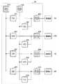
次に、電源装置35について詳しく説明する。図3は従来の電源装置39の構成を示す概念図である。電源装置39は、トランス91、92、整流回路201及び202、交流回路203を備えて構成される。トランス91は不図示の交流電源から交流電圧を入力して変圧し、この変圧された交流電圧を整流回路201が正の直流電圧に変換する。同様に、トランス92は不図示の交流電源から交流電圧を入力して変圧し、この変圧された交流電圧を整流回路202が負の直流電圧に変換する。 Next, the
そして正の直流電圧と負の直流電圧を重畳させ、重畳させた直流電圧を交流回路203に含まれるトランスの二次側に入力する。即ち、交流回路203に含まれるトランスから出力される交流電圧と整流回路201及び202から出力された正負の直流電圧を重畳させた直流電圧を更に重畳させる。この直流電圧と交流電圧とが重畳された電圧は各現像部6へ供給される。 Then, a positive DC voltage and a negative DC voltage are superimposed, and the superimposed DC voltage is input to the secondary side of the transformer included in the
従来は、1つの現像部6に対して1つの電源装置39を配置していた。従って、プリンタ1のようなカラープリンタでは、現像部6が複数存在するために電源装置39も複数必要となり、その分電源装置39を構成するトランス等の部品数も増加してしまう。そのため、コスト削減が難しかったり、装置の小型化を困難にさせたりする等の問題があった。Conventionally, one
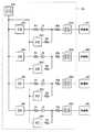
そこで、本発明では図4に示すような電源装置35を提案する。電源装置35は、トランス301及び302、整流回路201及び202、交流回路203を備えて構成される。トランス301は不図示の交流電源から交流電圧を入力して変圧し、この変圧した交流電圧を4つの整流回路201に供給する。同様に、トランス302は不図示の交流電源から交流電圧を入力して変圧し、この変圧した交流電圧を4つの整流回路202に供給する。整流回路201は入力した交流電圧を正の直流電圧に変換し、整流回路202は入力した交流電圧を負の直流電圧に変換する。Therefore, the present invention proposes a
そして正の直流電圧と負の直流電圧を重畳させ、交流回路203に含まれるトランスの二次側に入力する。即ち、交流回路203に含まれるトランスから出力される交流電圧と整流回路201及び202から出力された正負の直流電圧を重畳させた直流電圧を更に重畳させる。そしてこの直流電圧と交流電圧とが重畳された電圧を各現像部6へ供給する。 Then, a positive DC voltage and a negative DC voltage are superimposed and input to the secondary side of the transformer included in the
ここで、トランス301及び302、整流回路201及び202、交流回路203には制御部31から各色に応じた制御信号が入力され、各要素はこの制御信号に従って動作制御がなされる。つまり、各要素は制御信号に従って駆動し、出力する電圧レベル等を調整する。また、トランス301と整流回路201が第1直流電源に相当し、トランス302と整流回路202が第2直流電源に相当する。 Here, the control signals corresponding to the respective colors are input from the
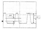
図5は現像部6へ供給される電圧波形を示した図である。電圧の周波数は3kHz、正デューティ30%、ピーク電圧1.6kVの交流電圧に+200Vの直流電圧を重畳させることによりシフトさせたものである。周波数、デューティ、ピーク電圧及びシフト量は画像形成時の条件により適宜制御されるものである。 FIG. 5 is a diagram showing a voltage waveform supplied to the developing
このように複数の整流回路201及び202に交流電圧を供給するトランスを共通化させることによって、従来は8つのトランスが必要であったものを2つにすることができる。つまり、トランスの個数が減ることによってコスト削減や、電源装置35の小型化を実現することができる。 In this way, by sharing a transformer that supplies an AC voltage to the plurality of
尚、本発明は上記実施の形態の構成に限られず種々の変形が可能である。図6は図4の変形例である。図4に示す電源装置35は、整流回路201に交流電圧を供給するトランス301と整流器202に交流電圧を供給するトランス302の2つのトランスを備えた場合について説明したが、トランス301及び302を更に集約して、図6に示す電源装置35のように1つのトランス303が全ての整流回路201及び整流回路202に交流電圧を供給するようにしてもよい。こうすることによって、更にトランスの数を減らすことができる。 The present invention is not limited to the configuration of the above embodiment, and various modifications can be made. FIG. 6 is a modification of FIG. The
また、図7に示すように、整流回路201から出力した正の直流電圧と整流回路202から出力した負の直流電圧を抵抗R1、R2及びR3とツェナーダイオードDを介して重畳させてもよい。 Further, as shown in FIG. 7, the positive DC voltage output from the
具体的には、抵抗R1の一端は整流回路201の出力端子と接続し、他端はツェナーダイオードDのカソードと接続する。抵抗R2の一端は整流回路202の出力端子と接続し、他端はツェナーダイオードDのアノードと接続する。抵抗R3の一端はツェナーダイオードDのアノードと接続し、他端は交流回路203に含まれるトランスの二次側に接続する。このように整流回路201及び202の間にツェナーダイオードDを配置することによって、整流回路201側から整流回路202側へ電流が無駄に流れることを防止することができる。 Specifically, one end of the resistor R1 is connected to the output terminal of the
図8は図7の変形例であって、図5と同様に1つのトランス303で全ての整流回路201及び202に交流電圧を供給し、正負の直流電圧をツェナーダイオードDを介して重畳させる場合について示した図である。 FIG. 8 is a modification of FIG. 7, and in the same way as FIG. 5, a
更に、図9に示すように、整流回路を集約して1つにしてもよい。図9に示す電源装置35は、トランス303から出力された交流電圧を整流回路401及び402に供給する。整流回路401は入力した交流電圧を正の直流電圧に変換し、4つの制御回路501へ出力する。電圧制御回路501は制御部31から出力される制御信号に基づいて直流電圧を制御する。同様に、整流回路402は入力した交流電圧を負の直流電圧に変換し、4つの制御回路502へ出力する。電圧制御回路502は制御部31から出力される各色の制御信号に従って出力する直流電圧のレベル等を調整する。 Furthermore, as shown in FIG. 9, the rectifier circuits may be integrated into one. The
電圧制御回路501を出力した正の直流電圧と電圧制御回路502を出力した負の直流電圧は抵抗R1〜R3及びツェナーダイオードDを介して重畳され、交流回路203に含まれるトランスの二次側に入力する。このように整流回路を集約することによって、更にコストを削減し、装置の小型化を実現することができる。 The positive DC voltage output from the
以上、説明した電源装置35は現像部6に印加する電圧を生成するものとして説明したが、現像部6に限らず、例えば帯電部4に対して電圧を印加するものであってよい。 The
1 プリンタ
31 制御部
6 現像部
35 電源装置
303 トランス(第2変圧器)
302 トランス(第3変圧器)
201 整流器(第1整流器)
202 整流器(第2整流器)
203 交流回路(第1変圧器)
R1、R2、R3 抵抗
D ツェナーダイオード
501 電圧制御回路(第1電圧制御手段)
502 電圧制御回路(第2電圧制御手段)1
303 transformer (second transformer)
302 transformer (third transformer)
201 Rectifier (first rectifier)
202 Rectifier (second rectifier)
203 AC circuit (first transformer)
R1, R2, R3 Resistor
502 Voltage control circuit (second voltage control means)
Claims (1)
Translated fromJapanese入力電圧を変圧して前記複数の現像手段へ交流電圧を出力する複数の第1変圧器と、
1つの第2変圧器と、その第2変圧器から出力された交流電圧を正の直流電圧に変換して出力する第1整流器と、前記第2変圧器から出力された交流電圧を負の直流電圧に変換して出力する第2整流器とを有する直流電源と、
前記第1整流器から出力された正の直流電圧に対して電圧制御を行う前記複数の第1変圧器と同じ数の第1電圧制御手段と、
前記第2整流器から出力された負の直流電圧に対して電圧制御を行う前記複数の第1変圧器と同じ数の第2電圧制御手段と、
前記各第1電圧制御手段の出力端に、それぞれ一端が接続された複数の第1抵抗と、
前記各第1抵抗の他端に、それぞれカソードが接続された複数のツェナーダイオードと、
前記各第2電圧制御手段の出力端にそれぞれ一端が接続され、他端がそれぞれ前記各ツェナーダイオードのアノードに接続された複数の第2抵抗と、
前記各ツェナーダイオードのアノードと前記複数の第2抵抗との接続点で重畳された直流電圧を前記各第1変圧器から出力した交流電圧にそれぞれ重畳する複数の第3抵抗とを備えた画像形成装置。A plurality of developing means for developing the electrostatic latent image formed on the image carrier using a developer;
A plurality of first transformers for transforming an input voltage and outputting an alternating voltageto the plurality of developing means ;
One second transformer, a first rectifier that converts the AC voltage output from the second transformer into a positive DC voltage and outputs the positive voltage, and the AC voltage output from the second transformer is a negative DC voltage. A DC power supply having a second rectifier that converts the voltage to output;
The same number of first voltage control means as the plurality of first transformers for performing voltage control on the positive DC voltage output from the first rectifier;
The same number of second voltage control means as the plurality of first transformers for performing voltage control on the negative DC voltage output from the second rectifier;
A plurality of first resistors each having one end connected to an output end of each first voltage control means;
A plurality of Zener diodes each having a cathode connected to the other end of each first resistor;
A plurality of second resistors each having one end connected to the output end of each second voltage control means and the other end connected to the anode of each zener diode;
Image forming comprising: aplurality of third resistors for respectively superimposinga DC voltagesuperimposed at a connection point between the anode of each Zener diode and the plurality of second resistors on an AC voltage output from each of the first transformersapparatus.
Priority Applications (3)
| Application Number | Priority Date | Filing Date | Title |
|---|---|---|---|
| JP2008082544AJP5258344B2 (en) | 2008-03-27 | 2008-03-27 | Image forming apparatus |
| CN2009101323042ACN101546960B (en) | 2008-03-27 | 2009-03-25 | Power source apparatus |
| US12/410,956US8212380B2 (en) | 2008-03-27 | 2009-03-25 | Power source apparatus and image forming apparatus |
Applications Claiming Priority (1)
| Application Number | Priority Date | Filing Date | Title |
|---|---|---|---|
| JP2008082544AJP5258344B2 (en) | 2008-03-27 | 2008-03-27 | Image forming apparatus |
Publications (2)
| Publication Number | Publication Date |
|---|---|
| JP2009240064A JP2009240064A (en) | 2009-10-15 |
| JP5258344B2true JP5258344B2 (en) | 2013-08-07 |
Family
ID=41116942
Family Applications (1)
| Application Number | Title | Priority Date | Filing Date |
|---|---|---|---|
| JP2008082544AExpired - Fee RelatedJP5258344B2 (en) | 2008-03-27 | 2008-03-27 | Image forming apparatus |
Country Status (3)
| Country | Link |
|---|---|
| US (1) | US8212380B2 (en) |
| JP (1) | JP5258344B2 (en) |
| CN (1) | CN101546960B (en) |
Families Citing this family (6)
| Publication number | Priority date | Publication date | Assignee | Title |
|---|---|---|---|---|
| KR101258344B1 (en)* | 2008-10-31 | 2013-04-30 | 칼 짜이스 에스엠티 게엠베하 | Illuminating optic for euv microlithography |
| JP2011113405A (en)* | 2009-11-27 | 2011-06-09 | Sony Corp | Power supply apparatus, power supply method and power supply system |
| CN102538974A (en)* | 2012-01-12 | 2012-07-04 | 杭州美盛红外光电技术有限公司 | Thermal image display device, thermal image display system and thermal image display method |
| JP6035771B2 (en)* | 2012-02-20 | 2016-11-30 | 株式会社リコー | Transfer device and image forming apparatus |
| CN103197524B (en)* | 2012-12-28 | 2015-09-23 | 珠海天威飞马打印耗材有限公司 | A kind of device and method regulating developing bias |
| JP6093984B2 (en)* | 2014-03-19 | 2017-03-15 | コニカミノルタ株式会社 | Image forming apparatus |
Family Cites Families (16)
| Publication number | Priority date | Publication date | Assignee | Title |
|---|---|---|---|---|
| NL46063C (en)* | 1934-12-29 | |||
| JP2812824B2 (en)* | 1990-11-14 | 1998-10-22 | 三菱電機株式会社 | DC-DC converter |
| JPH06335247A (en)* | 1993-05-20 | 1994-12-02 | Canon Inc | Power supply |
| CA2249755C (en)* | 1998-10-02 | 2006-12-12 | Praveen K. Jain | Full bridge dc-dc converters |
| KR100503468B1 (en)* | 2002-10-08 | 2005-07-27 | 삼성전자주식회사 | Device for providing high voltage to develope print image of color laser printer |
| JP2004303466A (en)* | 2003-03-28 | 2004-10-28 | Canon Inc | Heater drive circuit |
| US7212419B2 (en)* | 2004-02-24 | 2007-05-01 | Vlt, Inc. | Adaptively configured and autoranging voltage transformation module arrays |
| CN2726727Y (en)* | 2004-09-30 | 2005-09-21 | 宋莲琴 | Alternating current/direct current superposing high-frequency pulse purification power supply |
| JP2006317524A (en) | 2005-05-10 | 2006-11-24 | Konica Minolta Business Technologies Inc | Developing device and image forming apparatus |
| KR100605260B1 (en) | 2005-07-15 | 2006-07-31 | 삼성전자주식회사 | AC high voltage measuring device |
| JP2007114386A (en)* | 2005-10-19 | 2007-05-10 | Ricoh Co Ltd | Voltage control method, charging device, image forming apparatus, and process cartridge |
| JP2007171936A (en)* | 2005-11-25 | 2007-07-05 | Kyocera Mita Corp | High-voltage power supply device and image forming apparatus |
| JP4480682B2 (en)* | 2006-01-26 | 2010-06-16 | 京セラミタ株式会社 | High voltage generation circuit |
| JP4908863B2 (en)* | 2006-02-02 | 2012-04-04 | キヤノン株式会社 | Image forming apparatus and high-voltage power supply apparatus |
| US7907864B2 (en)* | 2007-04-24 | 2011-03-15 | Samsung Electronics Co., Ltd. | High voltage power controlling apparatus of image forming apparatus including multiple DC power supplies |
| US7884588B2 (en)* | 2008-04-10 | 2011-02-08 | Stmicroelectronics S.R.L. | Control method and device for a system of interleaved converters using a designated master converter |
- 2008
- 2008-03-27JPJP2008082544Apatent/JP5258344B2/ennot_activeExpired - Fee Related
- 2009
- 2009-03-25USUS12/410,956patent/US8212380B2/ennot_activeExpired - Fee Related
- 2009-03-25CNCN2009101323042Apatent/CN101546960B/ennot_activeExpired - Fee Related
Also Published As
| Publication number | Publication date |
|---|---|
| US20090244941A1 (en) | 2009-10-01 |
| CN101546960B (en) | 2012-10-03 |
| US8212380B2 (en) | 2012-07-03 |
| CN101546960A (en) | 2009-09-30 |
| JP2009240064A (en) | 2009-10-15 |
Similar Documents
| Publication | Publication Date | Title |
|---|---|---|
| JP5258344B2 (en) | Image forming apparatus | |
| JP4396633B2 (en) | Image forming apparatus | |
| US8487475B2 (en) | Power supply apparatus and method of supplying power | |
| JP5880023B2 (en) | Power supply circuit, image forming apparatus | |
| JP6237190B2 (en) | Power supply control apparatus and image forming apparatus using the same | |
| JP2011139570A (en) | Multi-output power supply device and image forming device equipped with the power supply device | |
| JP5171689B2 (en) | Image forming apparatus | |
| JP2010048960A (en) | Image forming apparatus | |
| JP4192555B2 (en) | Image forming apparatus | |
| JP5212242B2 (en) | Image forming apparatus | |
| JP2017003718A (en) | Power supply circuit, image forming apparatus using the same, and development bias voltage application method of the image forming apparatus | |
| JP5588927B2 (en) | Image forming apparatus | |
| JP5337466B2 (en) | Power supply device and image forming apparatus provided with the same | |
| JP2013078187A (en) | Electronic apparatus | |
| US9977394B2 (en) | Power source device, image forming apparatus and voltage control method | |
| JP2011188625A (en) | Power unit, image forming apparatus using the same, method and program for controlling the power unit | |
| JP5530617B2 (en) | Power supply | |
| JP6577847B2 (en) | Heating apparatus and image forming apparatus | |
| JP2006162676A (en) | Process cartridge, image forming apparatus, and control method in image forming apparatus | |
| JP5172291B2 (en) | Power supply device and image forming apparatus | |
| JP2015012773A (en) | High-voltage power supply unit and image formation device | |
| JP2014180083A (en) | Power supply device | |
| JP2012047935A (en) | Image forming device | |
| JP2021052537A (en) | Power supply and power control method | |
| JP2020048364A (en) | Electric power unit and image formation device |
Legal Events
| Date | Code | Title | Description |
|---|---|---|---|
| A621 | Written request for application examination | Free format text:JAPANESE INTERMEDIATE CODE: A621 Effective date:20101122 | |
| A977 | Report on retrieval | Free format text:JAPANESE INTERMEDIATE CODE: A971007 Effective date:20120628 | |
| A131 | Notification of reasons for refusal | Free format text:JAPANESE INTERMEDIATE CODE: A131 Effective date:20120731 | |
| A521 | Request for written amendment filed | Free format text:JAPANESE INTERMEDIATE CODE: A523 Effective date:20120928 | |
| TRDD | Decision of grant or rejection written | ||
| A01 | Written decision to grant a patent or to grant a registration (utility model) | Free format text:JAPANESE INTERMEDIATE CODE: A01 Effective date:20130326 | |
| A61 | First payment of annual fees (during grant procedure) | Free format text:JAPANESE INTERMEDIATE CODE: A61 Effective date:20130423 | |
| FPAY | Renewal fee payment (event date is renewal date of database) | Free format text:PAYMENT UNTIL: 20160502 Year of fee payment:3 | |
| R150 | Certificate of patent or registration of utility model | Ref document number:5258344 Country of ref document:JP Free format text:JAPANESE INTERMEDIATE CODE: R150 Free format text:JAPANESE INTERMEDIATE CODE: R150 | |
| LAPS | Cancellation because of no payment of annual fees |