JP5258277B2 - Liquid crystal display - Google Patents
Liquid crystal displayDownload PDFInfo
- Publication number
- JP5258277B2 JP5258277B2JP2007321022AJP2007321022AJP5258277B2JP 5258277 B2JP5258277 B2JP 5258277B2JP 2007321022 AJP2007321022 AJP 2007321022AJP 2007321022 AJP2007321022 AJP 2007321022AJP 5258277 B2JP5258277 B2JP 5258277B2
- Authority
- JP
- Japan
- Prior art keywords
- contact hole
- substrate
- liquid crystal
- shielding layer
- layer
- Prior art date
- Legal status (The legal status is an assumption and is not a legal conclusion. Google has not performed a legal analysis and makes no representation as to the accuracy of the status listed.)
- Active
Links
- 239000004973liquid crystal related substanceSubstances0.000titleclaimsdescription144
- 239000000758substrateSubstances0.000claimsdescription246
- 239000010408filmSubstances0.000claimsdescription190
- 239000010409thin filmSubstances0.000claimsdescription90
- 239000011347resinSubstances0.000claimsdescription24
- 229920005989resinPolymers0.000claimsdescription24
- 239000000049pigmentSubstances0.000claimsdescription12
- 229910052751metalInorganic materials0.000claimsdescription10
- 239000002184metalSubstances0.000claimsdescription10
- 239000010410layerSubstances0.000description292
- 239000011159matrix materialSubstances0.000description93
- 238000000034methodMethods0.000description71
- XLOMVQKBTHCTTD-UHFFFAOYSA-NZinc monoxideChemical compound[Zn]=OXLOMVQKBTHCTTD-UHFFFAOYSA-N0.000description39
- -1polyethylene terephthalatePolymers0.000description28
- 239000011651chromiumSubstances0.000description27
- 229910003437indium oxideInorganic materials0.000description26
- PJXISJQVUVHSOJ-UHFFFAOYSA-Nindium(iii) oxideChemical compound[O-2].[O-2].[O-2].[In+3].[In+3]PJXISJQVUVHSOJ-UHFFFAOYSA-N0.000description26
- XOLBLPGZBRYERU-UHFFFAOYSA-Ntin dioxideChemical compoundO=[Sn]=OXOLBLPGZBRYERU-UHFFFAOYSA-N0.000description26
- 229910001887tin oxideInorganic materials0.000description26
- VYPSYNLAJGMNEJ-UHFFFAOYSA-NSilicium dioxideChemical compoundO=[Si]=OVYPSYNLAJGMNEJ-UHFFFAOYSA-N0.000description23
- AMGQUBHHOARCQH-UHFFFAOYSA-Nindium;oxotinChemical compound[In].[Sn]=OAMGQUBHHOARCQH-UHFFFAOYSA-N0.000description23
- 239000004695Polyether sulfoneSubstances0.000description18
- 229920003207poly(ethylene-2,6-naphthalate)Polymers0.000description18
- 229920006393polyether sulfonePolymers0.000description18
- 239000011112polyethylene naphthalateSubstances0.000description18
- 229920000139polyethylene terephthalatePolymers0.000description18
- 239000005020polyethylene terephthalateSubstances0.000description18
- 239000004065semiconductorSubstances0.000description14
- 229910052814silicon oxideInorganic materials0.000description14
- 229910006404SnO 2Inorganic materials0.000description13
- ZCLBLRDCYNGAGV-UHFFFAOYSA-N[Si]=O.[Sn].[In]Chemical compound[Si]=O.[Sn].[In]ZCLBLRDCYNGAGV-UHFFFAOYSA-N0.000description13
- 235000012489doughnutsNutrition0.000description13
- YVTHLONGBIQYBO-UHFFFAOYSA-Nzinc indium(3+) oxygen(2-)Chemical compound[O--].[Zn++].[In+3]YVTHLONGBIQYBO-UHFFFAOYSA-N0.000description13
- 239000011787zinc oxideSubstances0.000description13
- VYZAMTAEIAYCRO-UHFFFAOYSA-NChromiumChemical compound[Cr]VYZAMTAEIAYCRO-UHFFFAOYSA-N0.000description12
- 229910052804chromiumInorganic materials0.000description12
- 239000005262ferroelectric liquid crystals (FLCs)Substances0.000description12
- 239000011521glassSubstances0.000description12
- NIXOWILDQLNWCW-UHFFFAOYSA-Nacrylic acid groupChemical groupC(C=C)(=O)ONIXOWILDQLNWCW-UHFFFAOYSA-N0.000description11
- 238000004519manufacturing processMethods0.000description11
- 229920001721polyimidePolymers0.000description11
- 239000004743PolypropyleneSubstances0.000description9
- 239000005407aluminoborosilicate glassSubstances0.000description9
- 229910052788bariumInorganic materials0.000description9
- DSAJWYNOEDNPEQ-UHFFFAOYSA-Nbarium atomChemical compound[Ba]DSAJWYNOEDNPEQ-UHFFFAOYSA-N0.000description9
- 239000005388borosilicate glassSubstances0.000description9
- KPUWHANPEXNPJT-UHFFFAOYSA-NdisiloxaneChemical class[SiH3]O[SiH3]KPUWHANPEXNPJT-UHFFFAOYSA-N0.000description9
- 239000000463materialSubstances0.000description9
- 229920003023plasticPolymers0.000description9
- 239000004033plasticSubstances0.000description9
- 239000009719polyimide resinSubstances0.000description9
- 229920001155polypropylenePolymers0.000description9
- 125000001424substituent groupChemical group0.000description9
- 229920003002synthetic resinPolymers0.000description9
- 239000000057synthetic resinSubstances0.000description9
- UFHFLCQGNIYNRP-UHFFFAOYSA-NHydrogenChemical compound[H][H]UFHFLCQGNIYNRP-UHFFFAOYSA-N0.000description6
- 239000004988Nematic liquid crystalSubstances0.000description6
- 239000004990Smectic liquid crystalSubstances0.000description6
- 125000001153fluoro groupChemical groupF*0.000description6
- 229910052739hydrogenInorganic materials0.000description6
- 239000001257hydrogenSubstances0.000description6
- 125000000962organic groupChemical group0.000description6
- XUIMIQQOPSSXEZ-UHFFFAOYSA-NSiliconChemical compound[Si]XUIMIQQOPSSXEZ-UHFFFAOYSA-N0.000description5
- WGLPBDUCMAPZCE-UHFFFAOYSA-NTrioxochromiumChemical compoundO=[Cr](=O)=OWGLPBDUCMAPZCE-UHFFFAOYSA-N0.000description5
- 229910000423chromium oxideInorganic materials0.000description5
- 239000003086colorantSubstances0.000description5
- 229910052710siliconInorganic materials0.000description5
- 239000010703siliconSubstances0.000description5
- 239000002356single layerSubstances0.000description5
- 238000004040coloringMethods0.000description4
- 150000001875compoundsChemical class0.000description4
- 239000011229interlayerSubstances0.000description4
- 229920000642polymerPolymers0.000description4
- 230000001681protective effectEffects0.000description4
- 239000000565sealantSubstances0.000description4
- 239000003566sealing materialSubstances0.000description4
- 125000006850spacer groupChemical group0.000description4
- OKTJSMMVPCPJKN-UHFFFAOYSA-NCarbonChemical compound[C]OKTJSMMVPCPJKN-UHFFFAOYSA-N0.000description3
- 229910002808Si–O–SiInorganic materials0.000description3
- 125000000217alkyl groupChemical group0.000description3
- 125000003118aryl groupChemical group0.000description3
- QVGXLLKOCUKJST-UHFFFAOYSA-Natomic oxygenChemical compound[O]QVGXLLKOCUKJST-UHFFFAOYSA-N0.000description3
- 230000005540biological transmissionEffects0.000description3
- 229910052799carbonInorganic materials0.000description3
- 239000006185dispersionSubstances0.000description3
- 238000005530etchingMethods0.000description3
- RHZWSUVWRRXEJF-UHFFFAOYSA-Nindium tinChemical compound[In].[Sn]RHZWSUVWRRXEJF-UHFFFAOYSA-N0.000description3
- 229910052760oxygenInorganic materials0.000description3
- 239000001301oxygenSubstances0.000description3
- 239000007858starting materialSubstances0.000description3
- 239000012780transparent materialSubstances0.000description3
- 239000004642PolyimideSubstances0.000description2
- 239000004372Polyvinyl alcoholSubstances0.000description2
- 239000000853adhesiveSubstances0.000description2
- 230000001070adhesive effectEffects0.000description2
- 239000006229carbon blackSubstances0.000description2
- 238000000576coating methodMethods0.000description2
- 239000013078crystalSubstances0.000description2
- 239000012788optical filmSubstances0.000description2
- 229920002451polyvinyl alcoholPolymers0.000description2
- 229910000679solderInorganic materials0.000description2
- 238000004528spin coatingMethods0.000description2
- 238000004544sputter depositionMethods0.000description2
- 239000004593EpoxySubstances0.000description1
- BQCADISMDOOEFD-UHFFFAOYSA-NSilverChemical compound[Ag]BQCADISMDOOEFD-UHFFFAOYSA-N0.000description1
- 239000007864aqueous solutionSubstances0.000description1
- 238000009125cardiac resynchronization therapyMethods0.000description1
- 230000007547defectEffects0.000description1
- 238000010586diagramMethods0.000description1
- 238000001035dryingMethods0.000description1
- 238000004043dyeingMethods0.000description1
- 230000005684electric fieldEffects0.000description1
- 238000004070electrodepositionMethods0.000description1
- 230000002349favourable effectEffects0.000description1
- 230000001678irradiating effectEffects0.000description1
- 230000003287optical effectEffects0.000description1
- 239000003960organic solventSubstances0.000description1
- 238000000206photolithographyMethods0.000description1
- 229920002120photoresistant polymerPolymers0.000description1
- 238000002310reflectometryMethods0.000description1
- 238000007789sealingMethods0.000description1
- 229910052709silverInorganic materials0.000description1
- 239000004332silverSubstances0.000description1
- 239000002904solventSubstances0.000description1
- 238000001771vacuum depositionMethods0.000description1
- 238000007740vapor depositionMethods0.000description1
Images


Classifications
- G—PHYSICS
- G02—OPTICS
- G02F—OPTICAL DEVICES OR ARRANGEMENTS FOR THE CONTROL OF LIGHT BY MODIFICATION OF THE OPTICAL PROPERTIES OF THE MEDIA OF THE ELEMENTS INVOLVED THEREIN; NON-LINEAR OPTICS; FREQUENCY-CHANGING OF LIGHT; OPTICAL LOGIC ELEMENTS; OPTICAL ANALOGUE/DIGITAL CONVERTERS
- G02F1/00—Devices or arrangements for the control of the intensity, colour, phase, polarisation or direction of light arriving from an independent light source, e.g. switching, gating or modulating; Non-linear optics
- G02F1/01—Devices or arrangements for the control of the intensity, colour, phase, polarisation or direction of light arriving from an independent light source, e.g. switching, gating or modulating; Non-linear optics for the control of the intensity, phase, polarisation or colour
- G02F1/13—Devices or arrangements for the control of the intensity, colour, phase, polarisation or direction of light arriving from an independent light source, e.g. switching, gating or modulating; Non-linear optics for the control of the intensity, phase, polarisation or colour based on liquid crystals, e.g. single liquid crystal display cells
- G02F1/133—Constructional arrangements; Operation of liquid crystal cells; Circuit arrangements
- G02F1/136—Liquid crystal cells structurally associated with a semi-conducting layer or substrate, e.g. cells forming part of an integrated circuit
- G02F1/1362—Active matrix addressed cells
- G02F1/136209—Light shielding layers, e.g. black matrix, incorporated in the active matrix substrate, e.g. structurally associated with the switching element
- G—PHYSICS
- G02—OPTICS
- G02F—OPTICAL DEVICES OR ARRANGEMENTS FOR THE CONTROL OF LIGHT BY MODIFICATION OF THE OPTICAL PROPERTIES OF THE MEDIA OF THE ELEMENTS INVOLVED THEREIN; NON-LINEAR OPTICS; FREQUENCY-CHANGING OF LIGHT; OPTICAL LOGIC ELEMENTS; OPTICAL ANALOGUE/DIGITAL CONVERTERS
- G02F1/00—Devices or arrangements for the control of the intensity, colour, phase, polarisation or direction of light arriving from an independent light source, e.g. switching, gating or modulating; Non-linear optics
- G02F1/01—Devices or arrangements for the control of the intensity, colour, phase, polarisation or direction of light arriving from an independent light source, e.g. switching, gating or modulating; Non-linear optics for the control of the intensity, phase, polarisation or colour
- G02F1/13—Devices or arrangements for the control of the intensity, colour, phase, polarisation or direction of light arriving from an independent light source, e.g. switching, gating or modulating; Non-linear optics for the control of the intensity, phase, polarisation or colour based on liquid crystals, e.g. single liquid crystal display cells
- G02F1/133—Constructional arrangements; Operation of liquid crystal cells; Circuit arrangements
- G02F1/1333—Constructional arrangements; Manufacturing methods
- G02F1/1335—Structural association of cells with optical devices, e.g. polarisers or reflectors
- G02F1/133509—Filters, e.g. light shielding masks
- G02F1/133512—Light shielding layers, e.g. black matrix
- G—PHYSICS
- G02—OPTICS
- G02F—OPTICAL DEVICES OR ARRANGEMENTS FOR THE CONTROL OF LIGHT BY MODIFICATION OF THE OPTICAL PROPERTIES OF THE MEDIA OF THE ELEMENTS INVOLVED THEREIN; NON-LINEAR OPTICS; FREQUENCY-CHANGING OF LIGHT; OPTICAL LOGIC ELEMENTS; OPTICAL ANALOGUE/DIGITAL CONVERTERS
- G02F1/00—Devices or arrangements for the control of the intensity, colour, phase, polarisation or direction of light arriving from an independent light source, e.g. switching, gating or modulating; Non-linear optics
- G02F1/01—Devices or arrangements for the control of the intensity, colour, phase, polarisation or direction of light arriving from an independent light source, e.g. switching, gating or modulating; Non-linear optics for the control of the intensity, phase, polarisation or colour
- G02F1/13—Devices or arrangements for the control of the intensity, colour, phase, polarisation or direction of light arriving from an independent light source, e.g. switching, gating or modulating; Non-linear optics for the control of the intensity, phase, polarisation or colour based on liquid crystals, e.g. single liquid crystal display cells
- G02F1/133—Constructional arrangements; Operation of liquid crystal cells; Circuit arrangements
- G02F1/136—Liquid crystal cells structurally associated with a semi-conducting layer or substrate, e.g. cells forming part of an integrated circuit
- G02F1/1362—Active matrix addressed cells
- G02F1/136227—Through-hole connection of the pixel electrode to the active element through an insulation layer
- G—PHYSICS
- G02—OPTICS
- G02F—OPTICAL DEVICES OR ARRANGEMENTS FOR THE CONTROL OF LIGHT BY MODIFICATION OF THE OPTICAL PROPERTIES OF THE MEDIA OF THE ELEMENTS INVOLVED THEREIN; NON-LINEAR OPTICS; FREQUENCY-CHANGING OF LIGHT; OPTICAL LOGIC ELEMENTS; OPTICAL ANALOGUE/DIGITAL CONVERTERS
- G02F1/00—Devices or arrangements for the control of the intensity, colour, phase, polarisation or direction of light arriving from an independent light source, e.g. switching, gating or modulating; Non-linear optics
- G02F1/01—Devices or arrangements for the control of the intensity, colour, phase, polarisation or direction of light arriving from an independent light source, e.g. switching, gating or modulating; Non-linear optics for the control of the intensity, phase, polarisation or colour
- G02F1/13—Devices or arrangements for the control of the intensity, colour, phase, polarisation or direction of light arriving from an independent light source, e.g. switching, gating or modulating; Non-linear optics for the control of the intensity, phase, polarisation or colour based on liquid crystals, e.g. single liquid crystal display cells
- G02F1/133—Constructional arrangements; Operation of liquid crystal cells; Circuit arrangements
- G02F1/136—Liquid crystal cells structurally associated with a semi-conducting layer or substrate, e.g. cells forming part of an integrated circuit
- G02F1/1362—Active matrix addressed cells
- G02F1/1368—Active matrix addressed cells in which the switching element is a three-electrode device
Landscapes
- Physics & Mathematics (AREA)
- Nonlinear Science (AREA)
- Mathematical Physics (AREA)
- Chemical & Material Sciences (AREA)
- Crystallography & Structural Chemistry (AREA)
- General Physics & Mathematics (AREA)
- Optics & Photonics (AREA)
- Engineering & Computer Science (AREA)
- Microelectronics & Electronic Packaging (AREA)
- Liquid Crystal (AREA)
- Thin Film Transistor (AREA)
- Devices For Indicating Variable Information By Combining Individual Elements (AREA)
Description
Translated fromJapanese本発明は、アクティブマトリクス型の液晶表示装置に関する。 The present invention relates to an active matrix liquid crystal display device.
従来、薄膜トランジスタ(TFT)等の能動素子を用いたアクティブマトリクス型の液晶表示装置が知られている。アクティブマトリクス型の液晶表示装置は画素密度を高くすることが可能であり、小型軽量で、しかも低消費電力であることから、CRTに代わるフラットパネルディスプレイの一つとして、パーソナルコンピューターのモニター、液晶テレビ、カーナビゲーションのモニターなどの製品が開発されている。 Conventionally, an active matrix liquid crystal display device using an active element such as a thin film transistor (TFT) is known. An active matrix type liquid crystal display device can increase the pixel density, is small and light, and has low power consumption. Therefore, as one of the flat panel displays to replace CRTs, monitors for personal computers and liquid crystal televisions are used. Products such as car navigation monitors have been developed.
液晶表示装置は、複数の薄膜トランジスタ(TFT)や配線の他、第1の電極(画素電極)等を含む画素部が形成された基板(アクティブマトリクス基板)と、第2の電極(対向電極)、遮光層(ブラックマトリクス)、及び着色層(カラーフィルター)等が形成された基板(対向基板)とを貼り合わせ、これらの間に液晶を封入し、画素電極と対向電極との間に印加される電界によって液晶分子を配向させ、光源からの光量を制御することによって表示が行われている。 In addition to a plurality of thin film transistors (TFTs) and wiring, a liquid crystal display device includes a substrate (active matrix substrate) on which a pixel portion including a first electrode (pixel electrode) and the like, a second electrode (counter electrode), A light-shielding layer (black matrix) and a substrate (counter substrate) on which a colored layer (color filter) and the like are formed are bonded together, liquid crystal is sealed between them, and applied between the pixel electrode and the counter electrode. Display is performed by aligning liquid crystal molecules with an electric field and controlling the amount of light from the light source.
液晶表示装置において表示させる際、液晶分子の配向が乱れると高精細な画像表示ができない。液晶分子の配向を揃えるために、画素電極と対向電極との間の距離(セルギャップ)を均一化(平坦化)する必要がある。その方法としては、例えば、平坦化膜として、塗布法などにより絶縁膜を形成する方法がある(特許文献1参照)。特許文献1に記載された有機膜は、平坦化を目的とした有機絶縁膜であり、アクリル系透明有機膜である。図面等からわかるように、有機膜を用いた場合、有機膜の膜厚が厚いため、コンタクトホールが深くなってしまう。
特許文献1に記載されているように、平坦化のために用いる層間膜の膜厚は比較的厚いものとなる。層間膜の膜厚が厚いと、画素電極と薄膜トランジスタとを電気的に接続する配線を形成するためのコンタクトホールが深くなってしまう。コンタクトホールが深くなると、必然的に画素電極と対向電極との間の距離(セルギャップ)も長くなる。従って、コンタクトホールが形成された箇所では、層間膜の膜厚の分だけ液晶層の厚さが厚くなるため、コンタクトホールが形成された箇所と形成されていない箇所とでは、液晶層の厚さが大きく異なる。すなわち、コンタクトホールが形成された箇所周辺では液晶分子の配向乱れが起きやすい状態となっている。特に、コンタクトホールの縁では層間膜が傾斜しているため、液晶分子の配向が最も乱れやすくなっている。液晶分子の配向が乱れると、液晶ディスプレイでは色むらが生じてしまう。 As described in Patent Document 1, the film thickness of the interlayer film used for planarization is relatively thick. When the film thickness of the interlayer film is large, a contact hole for forming a wiring for electrically connecting the pixel electrode and the thin film transistor becomes deep. As the contact hole becomes deeper, the distance (cell gap) between the pixel electrode and the counter electrode inevitably increases. Accordingly, the thickness of the liquid crystal layer is increased by the thickness of the interlayer film at the position where the contact hole is formed. Therefore, the thickness of the liquid crystal layer is increased between the position where the contact hole is formed and the position where the contact hole is not formed. Are very different. That is, the alignment disorder of the liquid crystal molecules is likely to occur around the portion where the contact hole is formed. Particularly, since the interlayer film is inclined at the edge of the contact hole, the alignment of the liquid crystal molecules is most easily disturbed. If the alignment of the liquid crystal molecules is disturbed, color unevenness occurs in the liquid crystal display.
そこで、本発明では、色むらを解消し、視認性が高く、高画質の液晶表示装置を提供することを目的とする。 Accordingly, an object of the present invention is to provide a liquid crystal display device that eliminates color unevenness, has high visibility, and has high image quality.
また、本発明では、色むらを解消し、かつ、開口率の高い高画質の液晶表示装置を提供することを目的とする。 It is another object of the present invention to provide a high-quality liquid crystal display device that eliminates color unevenness and has a high aperture ratio.
本発明の液晶表示装置は、薄膜トランジスタと、薄膜トランジスタと電気的に接続した導電層と、導電層上に設けられ、コンタクトホールを有する絶縁膜と、導電層及びコンタクトホールを有する絶縁膜上に設けられ、コンタクトホールを介して導電層と電気的に接続した画素電極と、少なくともコンタクトホールの縁と重なる領域に設けられた遮光層と、を有することを特徴とする。 The liquid crystal display device of the present invention is provided on a thin film transistor, a conductive layer electrically connected to the thin film transistor, an insulating film having a contact hole, and an insulating film having a contact hole and a conductive layer. And a pixel electrode electrically connected to the conductive layer through the contact hole, and a light shielding layer provided at least in a region overlapping with the edge of the contact hole.
本発明の液晶表示装置は、薄膜トランジスタと、薄膜トランジスタと電気的に接続した導電層と、導電層上に設けられ、コンタクトホールを有する絶縁膜と、導電層及びコンタクトホールを有する絶縁膜上に設けられ、コンタクトホールを介して導電層と電気的に接続した画素電極と、開口部を有する着色層と、を有し、着色層の開口部は、少なくともコンタクトホールの縁と重なる領域に設けられることを特徴とする。 The liquid crystal display device of the present invention is provided on a thin film transistor, a conductive layer electrically connected to the thin film transistor, an insulating film having a contact hole, and an insulating film having a contact hole and a conductive layer. A pixel electrode electrically connected to the conductive layer through the contact hole, and a colored layer having an opening, the opening of the colored layer being provided at least in a region overlapping with the edge of the contact hole Features.
本発明の液晶表示装置は、薄膜トランジスタと、薄膜トランジスタと電気的に接続した導電層と、導電層上に設けられ、コンタクトホールを有する絶縁膜と、導電層及びコンタクトホールを有する絶縁膜上に設けられ、コンタクトホールを介して導電層と電気的に接続した画素電極と、開口部を有する着色層と、少なくともコンタクトホールの縁と重なる領域に設けられた遮光層と、を有し、着色層の開口部は、少なくともコンタクトホールの縁と重なる領域に設けられることを特徴とする。 The liquid crystal display device of the present invention is provided on a thin film transistor, a conductive layer electrically connected to the thin film transistor, an insulating film having a contact hole, and an insulating film having a contact hole and a conductive layer. A pixel electrode electrically connected to the conductive layer through the contact hole, a colored layer having an opening, and a light-shielding layer provided at least in a region overlapping with the edge of the contact hole. The portion is provided at least in a region overlapping with the edge of the contact hole.
上記構成において、遮光層は、遮光性の金属膜、顔料または染料を分散させた樹脂膜であることを特徴とする。 In the above structure, the light shielding layer is a resin film in which a light shielding metal film, a pigment, or a dye is dispersed.
上記構成において、絶縁膜は、樹脂膜であることを特徴とする。 In the above structure, the insulating film is a resin film.
本発明の液晶表示装置は、液晶分子の配向が乱れている部分を表示部として機能させないことを特徴とする。 The liquid crystal display device of the present invention is characterized in that a portion where the alignment of liquid crystal molecules is disturbed does not function as a display portion.
本発明の液晶表示装置において、コンタクトホールを隠すように選択的に遮光層が形成されており、色むらのないディスプレイを提供することができる。 In the liquid crystal display device of the present invention, a light shielding layer is selectively formed so as to hide the contact hole, and a display having no color unevenness can be provided.
本発明の液晶表示装置において、コンタクトホール部分の液晶分子の配向乱れを反映させないように選択的にカラーフィルターを除去するため、色むらのないディスプレイを提供することができる。 In the liquid crystal display device of the present invention, since the color filter is selectively removed so as not to reflect the alignment disorder of the liquid crystal molecules in the contact hole portion, a display without color unevenness can be provided.
以下に、本発明の一態様について図面等を用いながら詳細に説明する。ただし、本発明は多くの異なる態様で実施することが可能であり、本発明の趣旨及びその範囲から逸脱することなくその形態及び詳細を様々に変更し得ることは当業者であれば容易に理解される。従って、本実施の形態の記載内容に限定して解釈されるものではない。 Hereinafter, one embodiment of the present invention will be described in detail with reference to the drawings. However, the present invention can be implemented in many different modes, and those skilled in the art can easily understand that the modes and details can be variously changed without departing from the spirit and scope of the present invention. Is done. Therefore, the present invention is not construed as being limited to the description of this embodiment mode.
(実施の形態1)
本実施の形態では、本発明を用いた液晶表示装置の構成について説明する。(Embodiment 1)
In this embodiment mode, a structure of a liquid crystal display device using the present invention will be described.
液晶分子の配向が乱れている部分を表示部として機能させない方法は、大きく分けて2つある。1つは、液晶分子の配向が乱れている部分を隠すように遮光層を設ける構成である。もう1つは、液晶分子の配向が乱れている部分にカラーフィルターを設けない構成である。 There are roughly two methods for preventing a portion where the alignment of liquid crystal molecules is disturbed from functioning as a display portion. One is a configuration in which a light shielding layer is provided so as to hide a portion where the alignment of liquid crystal molecules is disturbed. The other is a configuration in which a color filter is not provided in a portion where the alignment of liquid crystal molecules is disturbed.
液晶分子の配向が乱れている部分を隠すように遮光層を設ける構成としては、丸型とドーナツ型とがある。丸型とはコンタクトホール全体を覆う構成であり、ドーナツ型とはコンタクトホールの中心部分を除いた部分を遮光層で覆う構成である。ドーナツ型では、少なくともコンタクトホールの縁を覆う形状が好ましい。なお、コンタクトホールの縁とは、コンタクトホールのうち絶縁膜が傾斜している領域を指す。 There are a round shape and a donut shape as a structure in which the light shielding layer is provided so as to hide the portion where the alignment of liquid crystal molecules is disturbed. The round shape is a configuration that covers the entire contact hole, and the donut shape is a configuration that covers a portion excluding the central portion of the contact hole with a light shielding layer. In the donut shape, a shape covering at least the edge of the contact hole is preferable. Note that the edge of the contact hole refers to a region of the contact hole where the insulating film is inclined.
遮光層を丸型に形成した場合、コンタクトホール全体を覆っているため、液晶分子の配向が乱れた部分全体を隠すことができる。この構成とすることにより、色むらがなく、かつ開口率の高いディスプレイを作製することができる。また、この丸型の遮光層は、配線部分に遮光層を形成する工程と同じプロセスで形成することができるため、工程数の増加もなく、複雑なプロセスを用いる必要もない。 When the light shielding layer is formed in a round shape, the entire contact hole is covered, so that the entire portion where the alignment of liquid crystal molecules is disturbed can be hidden. With this structure, a display with no color unevenness and a high aperture ratio can be manufactured. Further, since this round light shielding layer can be formed by the same process as the process of forming the light shielding layer in the wiring portion, there is no increase in the number of steps and there is no need to use a complicated process.
遮光層をドーナツ型に形成した場合、コンタクトホールの縁、すなわちコンタクトホールのうち絶縁膜が傾斜している領域を覆っているため、液晶分子の配向が最も乱れやすい部分であるコンタクトホールの縁の配向乱れを隠すことができる。コンタクトホールの縁以外の部分では、液晶層の厚さの変化がほとんどないため、その部分では液晶分子の配向は乱れないと考えられる。この構成とすることにより、色むらがなく、かつ開口率の高いディスプレイを作製することができる。また、このドーナツ型の遮光層は、配線部分に遮光層を形成する工程と同じプロセスで形成することができるため、工程数の増加もなく、複雑なプロセスを用いる必要もない。なお、本明細書では、遮光層の形状を「丸型」「ドーナツ型」と記載しているが、コンタクトホールの形状に合わせて適宜変更することができる。すなわち、コンタクトホールを覆うという意図で設けてあればどのような形状であってもよく、例えば、円形、楕円形、正方形、長方形、三角形などが挙げられる。 When the light shielding layer is formed in a donut shape, it covers the edge of the contact hole, i.e., the region of the contact hole where the insulating film is inclined. The orientation disorder can be hidden. Since there is almost no change in the thickness of the liquid crystal layer in the portion other than the edge of the contact hole, it is considered that the alignment of the liquid crystal molecules is not disturbed in that portion. With this structure, a display with no color unevenness and a high aperture ratio can be manufactured. In addition, since the donut-shaped light shielding layer can be formed by the same process as the process of forming the light shielding layer in the wiring portion, there is no increase in the number of steps and there is no need to use a complicated process. In this specification, the shape of the light shielding layer is described as “round” or “doughnut”, but can be appropriately changed according to the shape of the contact hole. That is, any shape may be used as long as it is provided so as to cover the contact hole, and examples thereof include a circle, an ellipse, a square, a rectangle, and a triangle.
液晶分子の配向が乱れている部分にカラーフィルターを設けない構成としては、丸型とドーナツ型とがある。丸型とはコンタクトホール全体の上部にカラーフィルターを設けない構成であり、ドーナツ型とはコンタクトホールの縁、すなわちコンタクトホールのうち絶縁膜が傾斜している領域の上方にカラーフィルターを設けない構成である。 As a configuration in which a color filter is not provided in a portion where the alignment of liquid crystal molecules is disturbed, there are a round shape and a donut shape. The round type is a configuration in which no color filter is provided above the entire contact hole, and the donut type is a configuration in which no color filter is provided above the edge of the contact hole, that is, above the region of the contact hole where the insulating film is inclined. It is.
カラーフィルターを丸型に除去する場合、コンタクトホール全体にカラーフィルターが存在しないため、液晶層の厚さが大きく異なり、液晶分子の配向が乱れた部分を反映させない構成になる。この構成とすることにより、色むらがなく、かつ開口率の高いディスプレイを作製することができる。また、カラーフィルターを丸型に除去する構成は、工程数の増加もなく、複雑なプロセスを用いる必要もない。 When the color filter is removed in a round shape, since the color filter does not exist in the entire contact hole, the thickness of the liquid crystal layer is greatly different, and the portion where the alignment of the liquid crystal molecules is disturbed is not reflected. With this structure, a display with no color unevenness and a high aperture ratio can be manufactured. Further, the configuration in which the color filter is removed in a round shape does not increase the number of steps and does not require a complicated process.
カラーフィルターをドーナツ型に除去する場合、コンタクトホールの縁、すなわちコンタクトホールのうち絶縁膜が傾斜している領域のカラーフィルターを除去する。コンタクトホールの縁以外の部分では、液晶層の厚さの変化がほとんどないため、その部分では液晶分子の配向は乱れないと考えられる。この構成とすることにより、色むらがなく、かつ開口率の高いディスプレイを作製することができる。また、カラーフィルターをドーナツ型に除去する構成は、工程数の増加もなく、複雑なプロセスを用いる必要もない。なお、本明細書では、カラーフィルターの形状を「丸型」「ドーナツ型」と記載しているが、コンタクトホールの形状に合わせて適宜変更することができる。すなわち、コンタクトホールと重なる領域のカラーフィルターを除去するという意図で除去してあればどのような形状であってもよく、例えば、円形、楕円形、正方形、長方形、三角形などが挙げられる。 When the color filter is removed in a donut shape, the color filter is removed from the edge of the contact hole, that is, the region of the contact hole where the insulating film is inclined. Since there is almost no change in the thickness of the liquid crystal layer in the portion other than the edge of the contact hole, it is considered that the alignment of the liquid crystal molecules is not disturbed in that portion. With this structure, a display with no color unevenness and a high aperture ratio can be manufactured. Further, the configuration in which the color filter is removed in a donut shape does not increase the number of steps and does not require a complicated process. In this specification, the shape of the color filter is described as “round shape” or “doughnut shape”, but can be appropriately changed according to the shape of the contact hole. That is, any shape may be used as long as it is removed with the intention of removing the color filter in the region overlapping with the contact hole, and examples thereof include a circle, an ellipse, a square, a rectangle, and a triangle.
(実施の形態2)
本実施の形態では、選択的に遮光層を形成した液晶表示装置について、図1及び図2を用いて説明する。(Embodiment 2)
In this embodiment, a liquid crystal display device in which a light-blocking layer is selectively formed is described with reference to FIGS.
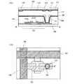
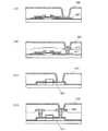
図1(B)は、本発明を適用した液晶表示装置を対向基板側から見た上面図である。アクティブマトリクス基板は、基板上に、薄膜トランジスタ、薄膜トランジスタに電気的に接続した配線層、絶縁膜、画素電極、配向膜等が形成されている。アクティブマトリクス基板と貼り合わせる対向基板は、基板上に、遮光層、対向電極、配向膜等が形成されている。図1(B)においては、ゲート線151、ソース線152、コンタクトホール103、薄膜トランジスタの半導体層154、第1の遮光層108、及び第2の遮光層109のみを図示し、それ以外は省略した。 FIG. 1B is a top view of the liquid crystal display device to which the present invention is applied as viewed from the counter substrate side. In the active matrix substrate, a thin film transistor, a wiring layer electrically connected to the thin film transistor, an insulating film, a pixel electrode, an alignment film, and the like are formed on the substrate. The counter substrate to be bonded to the active matrix substrate has a light shielding layer, a counter electrode, an alignment film, and the like formed on the substrate. In FIG. 1B, only the
図1(B)に示したように、遮光層として、ゲート線151及びソース線152に対応する領域に形成される第1の遮光層108と、薄膜トランジスタのソース領域又はドレイン領域のコンタクトホール103に対応する領域に形成される第2の遮光層109が形成される。 As shown in FIG. 1B, as a light shielding layer, the first
図1(A)は、コンタクトホール部分を拡大した図であり、図1(B)のA−A’で切った断面図である。本実施の形態のアクティブマトリクス基板の構成について以下に説明する。 FIG. 1A is an enlarged view of a contact hole portion, and is a cross-sectional view taken along A-A ′ in FIG. The structure of the active matrix substrate of this embodiment will be described below.
基板100上に薄膜トランジスタ101が形成されている。基板100としては、アルミノホウケイ酸ガラス、バリウムホウケイ酸ガラス、石英ガラス等のガラス基板の他、PET(ポリエチレンテレフタレート)、PEN(ポリエチレンナフタレート)、PES(ポリエーテルスルホン)、ポリプロピレンに代表されるプラスチックや、アクリルなどに代表される合成樹脂を原料とする基板を用いることができる。薄膜トランジスタ101は、トップゲート型、ボトムゲート型、チャネルエッチ型、チャネル保護型、いずれでも良いが、図1(A)ではチャネルエッチ型トランジスタを図示した。 A
薄膜トランジスタ101上に絶縁膜102を形成し、薄膜トランジスタ101と電気的に接続するためのコンタクトホール103を形成する。絶縁膜102には、有機樹脂膜、無機絶縁膜、またはシロキサン系材料を出発材料として形成されたSi−O−Si結合を含む絶縁膜(シロキサン系絶縁膜)を用いて形成することができる。ここで、シロキサンとは、シリコン(Si)と酸素(O)との結合で骨格構造が構成されるものであって、置換基として、少なくとも水素を含む有機基(例えばアルキル基、アリール基)が用いられる。また、置換基として、フルオロ基を用いてもよい。または、置換基として、少なくとも水素を含む有機基と、フルオロ基とを用いてもよい。また、低誘電率材料を絶縁膜に用いてもよい。 An insulating
なお、基板に対して垂直にコンタクトホール103を形成することも可能である。しかし、後工程で画素電極104を形成する際のステップカバレッジを向上させるためには、図1(A)に示したように、コンタクトホール103の縁が傾斜するように開口することが好ましい。よって、本明細書においては、コンタクトホールは傾斜部を有するものとし、その傾斜部をコンタクトホールの縁と表記する。 Note that the
薄膜トランジスタ101及び絶縁膜102を覆うように、画素電極104が形成される。画素電極104は、露出した薄膜トランジスタ101のドレイン電極105bと電気的に接続している。 A
反射型の液晶表示装置を作製する場合には、画素電極104として反射性を有する金属を用いることができる。透過型の液晶表示装置を作製する場合には、酸化インジウムに酸化スズを混合したインジウムスズ酸化物(ITO)、インジウムスズ酸化物(ITO)に酸化珪素を混合したインジウムスズ珪素酸化物(ITSO)、酸化インジウムに酸化亜鉛を混合したインジウム亜鉛酸化物(IZO)、酸化亜鉛(ZnO)、または酸化スズ(SnO2)等を用いることができる。半透過型の液晶表示装置を作製する場合、反射領域には反射性を有する金属を画素電極に用い、透過領域には透光性を有する材料(例えば、酸化インジウムに酸化スズを混合したインジウムスズ酸化物(ITO)、インジウムスズ酸化物(ITO)に酸化珪素を混合したインジウムスズ珪素酸化物(ITSO)、酸化インジウムに酸化亜鉛を混合したインジウム亜鉛酸化物(IZO)、酸化亜鉛(ZnO)、または酸化スズ(SnO2)等)を用いることができる。In the case of manufacturing a reflective liquid crystal display device, a metal having reflectivity can be used for the
画素電極104上に配向膜106が形成されている。配向膜106には、ポリイミド樹脂等を用いることができる。 An
次に、本実施の形態の対向基板の構成について説明する。 Next, the structure of the counter substrate of this embodiment will be described.
基板107に接して第1の遮光層108及び第2の遮光層109が形成されている。第1の遮光層108は、ソース配線を覆うように形成され、ソース電極105aの一部を覆うように形成される。第2の遮光層109は、コンタクトホール103に合わせて形成される。基板107には、アルミノホウケイ酸ガラス、バリウムホウケイ酸ガラス、石英ガラス等のガラス基板の他、PET(ポリエチレンテレフタレート)、PEN(ポリエチレンナフタレート)、PES(ポリエーテルスルホン)、ポリプロピレンに代表されるプラスチックや、アクリルなどに代表される合成樹脂を原料とする基板を用いることができる。第1の遮光層108及び第2の遮光層109には、遮光性の膜(例えば、クロム(Cr)の単層膜、酸化クロム(CrxOy)とクロム(Cr)の積層膜、カーボンブラックなどの顔料、染料等を分散させた樹脂膜等)を用いることができる。A first
図1(B)で示したように、遮光層としては、アクティブマトリクス基板上のゲート線151及びソース線152に対応する領域に形成される第1の遮光層108と、アクティブマトリクス基板上の薄膜トランジスタのソース領域又はドレイン領域のコンタクトホール103に対応する領域に形成される第2の遮光層109の2つが形成される。コンタクトホール103に対応する領域とは、コンタクトホール103と重なる領域を指す。 As shown in FIG. 1B, the light shielding layer includes a first
第2の遮光層109は、ゲート線151及びソース線152に対応する領域に形成される第1の遮光層108とは独立して、アクティブマトリクス基板のコンタクトホール103に対応する領域に形成される。したがって、その領域は表示部として機能しないため、コンタクトホール103の上層に存在する液晶分子の配向状態が乱れていても、色むらがなく、コントラストの高い、高画質な表示装置を作製することが可能となる。 The second
また、第1の遮光層108は、ゲート線151及びソース線152の上方に設けられているが、薄膜トランジスタ全体は覆っていない。このような構成であるため、開口率の低下を最小限に抑えることができる。 In addition, the first
遮光層を第1の遮光層108と第2の遮光層109の2つに分けて形成することにより、開口率の低下を最小限に抑えることができ、色むらがなく、コントラストの高い、高画質な表示装置を作製することができる。 By forming the light shielding layer in two parts, the first
第2の遮光層109の形状は、アクティブマトリクス基板のコンタクトホール103に対応する領域に設けられていればどのような形状であってもよい。例えば、円形、楕円形、正方形、長方形、三角形などが挙げられる。 The shape of the second
基板107、第1の遮光層108、及び第2の遮光層109に接して対向電極110が形成されている。対向電極110には、酸化インジウムに酸化スズを混合したインジウムスズ酸化物(ITO)、インジウムスズ酸化物(ITO)に酸化珪素を混合したインジウムスズ珪素酸化物(ITSO)、酸化インジウムに酸化亜鉛を混合したインジウム亜鉛酸化物(IZO)、酸化亜鉛(ZnO)、または酸化スズ(SnO2)等を用いることができる。A
対向電極110上に配向膜111が形成されている。配向膜111には、ポリイミド樹脂等を用いることができる。 An
上述の構成のアクティブマトリクス基板と対向基板とを貼り合わせ、アクティブマトリクス基板と対向基板との間に液晶層112を形成する。液晶には、強誘電性液晶(FLC)、ネマティック液晶、スメクティック液晶、ホモジニアス配向になるような液晶、ホメオトロピック配向になるような液晶等を用いることができる。 The active matrix substrate having the above structure and the counter substrate are bonded to each other, and the
なお、図1(A)及び(B)に示した構成とした場合、図7に示したように、第2の遮光層402は第1の遮光層401と独立して設けられることとなる。 1A and 1B, the second light-
図1(A)及び(B)の構成に加えて、アクティブマトリクス基板側に着色層(カラーフィルター)を形成してもよく、対向基板側に着色層(カラーフィルター)を形成してもよい。また、着色層(カラーフィルター)を形成する場合、単色でも複数色でもよい。 In addition to the structures shown in FIGS. 1A and 1B, a colored layer (color filter) may be formed on the active matrix substrate side, or a colored layer (color filter) may be formed on the counter substrate side. Moreover, when forming a colored layer (color filter), a single color or multiple colors may be sufficient.
アクティブマトリクス基板に形成する薄膜トランジスタは、トップゲート型、ボトムゲート型、チャネルエッチ型、チャネル保護型、いずれでも良い。また、薄膜トランジスタのソース電極又はドレイン電極が、画素電極と直接接続していなくてもよい。図9(A)に示したのは、図1(A)に示した構成である。図9(A)では、チャネルエッチ型のトランジスタのソース電極又はドレイン電極601に画素電極602が接している。図9(B)に示したのは、図9(A)に示したチャネルエッチ型の薄膜トランジスタのソース電極又はドレイン電極611と画素電極612とが、導電層613を介して、電気的に接続した構成である。 A thin film transistor formed over the active matrix substrate may be any of a top gate type, a bottom gate type, a channel etch type, and a channel protection type. Further, the source electrode or the drain electrode of the thin film transistor may not be directly connected to the pixel electrode. FIG. 9A shows the configuration shown in FIG. In FIG. 9A, the
図9(C)に示したのは、トップゲート型の薄膜トランジスタであって、薄膜トランジスタのソース領域又はドレイン領域621と画素電極622が接した構成である。図9(D)に示したのは、図9(C)に示したトップゲート型の薄膜トランジスタのソース領域又はドレイン領域631と画素電極632とが、導電層633を介して、電気的に接続した構成である。 FIG. 9C illustrates a top-gate thin film transistor in which a source or drain
なお、図9(A)〜(D)に示した薄膜トランジスタは一例である。本実施の形態では、ガラス基板上に形成した薄膜トランジスタを示したが、本発明に用いることができる薄膜トランジスタはこれらに限定されず、シリコンウェハを用いたトランジスタを用いることもできる。 Note that the thin film transistors illustrated in FIGS. 9A to 9D are examples. In this embodiment mode, a thin film transistor formed over a glass substrate is described; however, a thin film transistor that can be used in the present invention is not limited thereto, and a transistor using a silicon wafer can also be used.
図1(A)及び(B)に示した構成とすることによって、コンタクトホール103の上部で乱れた液晶分子の配向が画像表示に反映されないため、色むらのないディスプレイを作製することができる。また、第2の遮光層109が選択的に形成されるため、開口率の低下を抑えることができる。また、アクティブマトリクス基板上のゲート線151及びソース線152に対応する領域に形成される第1の遮光層108を形成する工程と同じプロセスで形成することができるため、工程数の増加もなく、複雑なプロセスを用いる必要もない。 With the structure shown in FIGS. 1A and 1B, the orientation of liquid crystal molecules disturbed in the upper portion of the
また、コンタクトホール103のうち絶縁膜102が傾斜している部分に対応した領域、すなわちコンタクトホールの縁と重なる領域に遮光層を設ける構成とすることも可能である。液晶分子の配向は、絶縁膜102が傾斜している領域(コンタクトホールの縁)で最も乱れるからである。 Alternatively, a light shielding layer may be provided in a region corresponding to a portion of the
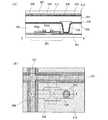
図2(B)は、本発明を適用した液晶表示装置を対向基板側から見た上面図である。第2の遮光層122を丸型ではなく、ドーナツ型とした点で図1(B)と異なっている。アクティブマトリクス基板として、基板上に、薄膜トランジスタ、薄膜トランジスタに電気的に接続した配線層、絶縁膜、画素電極、配向膜等が形成されている。アクティブマトリクス基板と貼り合わせる対向基板としては、基板上に、遮光層、対向電極、配向膜等が形成されている。図2(B)においては、ゲート線151、ソース線152、コンタクトホール153、薄膜トランジスタの半導体層154、第1の遮光層108、及び第2の遮光層122のみを図示し、それ以外は省略した。なお、図1(B)と共通しているものについては同様の符号を付した。 FIG. 2B is a top view of the liquid crystal display device to which the present invention is applied as viewed from the counter substrate side. 1B differs from FIG. 1B in that the second
図2(B)に示したように、遮光層は、ゲート線151及びソース線152に対応する領域に形成される第1の遮光層108と、薄膜トランジスタのソース領域又はドレイン領域のコンタクトホール153のうち絶縁膜が傾斜している部分121に対応した領域に形成される第2の遮光層122の2つが形成される。コンタクトホール153のうち絶縁膜が傾斜している部分121に対応した領域とは、コンタクトホール153の縁と重なる領域を指す。 As shown in FIG. 2B, the light shielding layer includes a first
図2(A)は、コンタクトホール部分を拡大した図であり、図2(B)のB−B’で切った断面図である。アクティブマトリクス基板の構成については、図1(A)及び(B)と同様であるため、ここでは説明を省略する。なお、図1(A)と共通しているものについては同様の符号を付した。 2A is an enlarged view of the contact hole portion, and is a cross-sectional view taken along B-B ′ in FIG. Since the structure of the active matrix substrate is the same as that in FIGS. 1A and 1B, description thereof is omitted here. In addition, the same code | symbol was attached | subjected about what is common in FIG. 1 (A).
対向基板の構成は以下のとおりである。基板107に接して第1の遮光層108及び第2の遮光層122が形成されている。第2の遮光層122はアクティブマトリクス基板に形成された絶縁膜102が傾斜している部分121に対応した領域に合わせて形成される。なお、絶縁膜102が傾斜している部分121に対応した領域とは、コンタクトホールの縁と重なる領域を指す。 The configuration of the counter substrate is as follows. A first
基板107には、アルミノホウケイ酸ガラス、バリウムホウケイ酸ガラス、石英ガラス等のガラス基板の他、PET(ポリエチレンテレフタレート)、PEN(ポリエチレンナフタレート)、PES(ポリエーテルスルホン)、ポリプロピレンに代表されるプラスチックや、アクリルなどに代表される合成樹脂を原料とする基板を用いることができる。第2の遮光層122には、遮光性の膜(例えば、クロム(Cr)の単層膜、酸化クロム(CrxOy)とクロム(Cr)の積層膜、カーボンブラックなどの顔料、染料等を分散させた樹脂膜等)を用いることができる。As the
基板107、第2の遮光層122に接して対向電極110が形成されている。対向電極110には、酸化インジウムに酸化スズを混合したインジウムスズ酸化物(ITO)、インジウムスズ酸化物(ITO)に酸化珪素を混合したインジウムスズ珪素酸化物(ITSO)、酸化インジウムに酸化亜鉛を混合したインジウム亜鉛酸化物(IZO)、酸化亜鉛(ZnO)、または酸化スズ(SnO2)等を用いることができる。A
対向電極110上に配向膜111が形成されている。配向膜111には、ポリイミド樹脂等を用いることができる。 An
上述の構成の対向基板と、図1(A)で説明したアクティブマトリクス基板とを貼り合わせ、アクティブマトリクス基板と対向基板との間に液晶を注入する。液晶には、強誘電性液晶(FLC)、ネマティック液晶、スメクティック液晶、ホモジニアス配向になるような液晶、ホメオトロピック配向になるような液晶等を用いることができる。 The counter substrate having the above structure is bonded to the active matrix substrate described with reference to FIG. 1A, and liquid crystal is injected between the active matrix substrate and the counter substrate. As the liquid crystal, a ferroelectric liquid crystal (FLC), a nematic liquid crystal, a smectic liquid crystal, a liquid crystal that has a homogeneous alignment, a liquid crystal that has a homeotropic alignment, or the like can be used.
図2(A)及び(B)の構成に加えて、アクティブマトリクス基板側に着色層(カラーフィルター)を形成してもよく、対向基板側に着色層(カラーフィルター)を形成してもよい。また、着色層(カラーフィルター)を形成する場合、単色でも複数色でもよい。 In addition to the structures shown in FIGS. 2A and 2B, a colored layer (color filter) may be formed on the active matrix substrate side, or a colored layer (color filter) may be formed on the counter substrate side. Moreover, when forming a colored layer (color filter), a single color or multiple colors may be sufficient.
アクティブマトリクス基板に形成する薄膜トランジスタは、トップゲート型、ボトムゲート型、チャネルエッチ型、チャネル保護型、いずれでも良い。また、薄膜トランジスタのソース電極又はドレイン電極が、画素電極と直接接続していなくてもよい。図2(A)及び(B)にも、図1(A)及び(B)と同様に図9(A)〜(D)に示したトランジスタを用いることができる。 A thin film transistor formed over the active matrix substrate may be any of a top gate type, a bottom gate type, a channel etch type, and a channel protection type. Further, the source electrode or the drain electrode of the thin film transistor may not be directly connected to the pixel electrode. The transistors shown in FIGS. 9A to 9D can be used in FIGS. 2A and 2B as well as FIGS. 1A and 1B.
図2(A)及び(B)に示した構成とすることによって、コンタクトホール153のうち絶縁膜102の傾斜している部分121、すなわちコンタクトホールの縁で乱れた液晶分子の配向が画像表示に反映されないため、色むらのないディスプレイを作製することができる。また、第2の遮光層122が選択的に形成されるため、開口率の低下を抑えることができる。また、アクティブマトリクス基板上のゲート線151及びソース線152に対応する領域に形成される第1の遮光層108を形成する工程と同じプロセスで形成することができるため、工程数の増加もなく、複雑なプロセスを用いる必要もない。 With the structure shown in FIGS. 2A and 2B, the orientation of the liquid crystal molecules disturbed at the
(実施の形態3)
本実施の形態では、選択的に着色層(カラーフィルター)を除去した液晶表示装置について、図3及び図4を用いて説明する。(Embodiment 3)
In this embodiment, a liquid crystal display device from which a colored layer (color filter) is selectively removed is described with reference to FIGS.
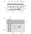
図3(B)は、本発明を適用した液晶表示装置を対向基板側から見た上面図である。アクティブマトリクス基板として、基板上に、薄膜トランジスタ、絶縁膜、画素電極、配向膜等が形成されている。アクティブマトリクス基板と貼り合わせる対向基板として、基板上に、遮光層、着色層、対向電極、配向膜等が形成されている。図3(B)においては、ゲート線251、ソース線252、コンタクトホール203、薄膜トランジスタの半導体層254、遮光層208、着色層(カラーフィルター)209のみを図示し、それ以外は省略した。 FIG. 3B is a top view of the liquid crystal display device to which the present invention is applied as viewed from the counter substrate side. As an active matrix substrate, a thin film transistor, an insulating film, a pixel electrode, an alignment film, and the like are formed on the substrate. As a counter substrate to be bonded to the active matrix substrate, a light shielding layer, a colored layer, a counter electrode, an alignment film, and the like are formed over the substrate. In FIG. 3B, only the
図3(B)に示したように、着色層(カラーフィルター)209は、アクティブマトリクス基板上の薄膜トランジスタのソース領域又はドレイン領域のコンタクトホール203に対応する領域が除去されている。コンタクトホール203に対応する領域とは、コンタクトホール203と重なる領域を指す。 As shown in FIG. 3B, the colored layer (color filter) 209 has a region corresponding to the
図3(A)は、コンタクトホール部分を拡大した図であり、図3(B)のC−C’で切った断面図である。本実施の形態のアクティブマトリクス基板の構成について以下に説明する。 FIG. 3A is an enlarged view of the contact hole portion, and is a cross-sectional view taken along C-C ′ in FIG. The structure of the active matrix substrate of this embodiment will be described below.
基板200上に薄膜トランジスタ201が形成されている。基板200としては、アルミノホウケイ酸ガラス、バリウムホウケイ酸ガラス、石英ガラス等のガラス基板の他、PET(ポリエチレンテレフタレート)、PEN(ポリエチレンナフタレート)、PES(ポリエーテルスルホン)、ポリプロピレンに代表されるプラスチックや、アクリルなどに代表される合成樹脂を原料とする基板を用いることができる。薄膜トランジスタ201は、トップゲート型、ボトムゲート型、チャネルエッチ型、チャネル保護型、いずれでも良いが、図3(A)ではチャネルエッチ型トランジスタを図示した。 A
薄膜トランジスタ201上に絶縁膜202を形成し、薄膜トランジスタ201と電気的に接続するためのコンタクトホール203を形成する。絶縁膜202には、有機樹脂膜、無機絶縁膜、またはシロキサン系材料を出発材料として形成されたSi−O−Si結合を含む絶縁膜(シロキサン系絶縁膜)を用いて形成することができる。ここで、シロキサンとは、シリコン(Si)と酸素(O)との結合で骨格構造が構成されるものであって、置換基として、少なくとも水素を含む有機基(例えばアルキル基、アリール基)が用いられる。また、置換基として、フルオロ基を用いてもよい。または、置換基として、少なくとも水素を含む有機基と、フルオロ基とを用いてもよい。また、低誘電率材料を絶縁膜に用いてもよい。 An insulating
薄膜トランジスタ201及び絶縁膜202を覆うように、画素電極204が形成される。画素電極204は、露出した薄膜トランジスタ201のドレイン電極205bと電気的に接続している。 A
反射型の液晶表示装置を作製する場合には、画素電極204として反射性を有する金属を用いることができる。透過型の液晶表示装置を作製する場合には、酸化インジウムに酸化スズを混合したインジウムスズ酸化物(ITO)、インジウムスズ酸化物(ITO)に酸化珪素を混合したインジウムスズ珪素酸化物(ITSO)、酸化インジウムに酸化亜鉛を混合したインジウム亜鉛酸化物(IZO)、酸化亜鉛(ZnO)、または酸化スズ(SnO2)等を用いることができる。半透過型の液晶表示装置を作製する場合、反射領域には反射性を有する金属を画素電極に用い、透過領域には透光性を有する材料(例えば、酸化インジウムに酸化スズを混合したインジウムスズ酸化物(ITO)、インジウムスズ酸化物(ITO)に酸化珪素を混合したインジウムスズ珪素酸化物(ITSO)、酸化インジウムに酸化亜鉛を混合したインジウム亜鉛酸化物(IZO)、酸化亜鉛(ZnO)、または酸化スズ(SnO2)等)を用いることができる。In the case of manufacturing a reflective liquid crystal display device, a reflective metal can be used for the
画素電極204上に配向膜206が形成されている。配向膜206には、ポリイミド樹脂等を用いることができる。 An
次に、本実施の形態の対向基板の構成について説明する。 Next, the structure of the counter substrate of this embodiment will be described.
基板207に接して、遮光層208及び着色層(カラーフィルター)209が形成されている。着色層(カラーフィルター)は、絶縁膜202に形成されたコンタクトホール203に合わせて除去される。基板207には、アルミノホウケイ酸ガラス、バリウムホウケイ酸ガラス、石英ガラス等のガラス基板の他、PET(ポリエチレンテレフタレート)、PEN(ポリエチレンナフタレート)、PES(ポリエーテルスルホン)、ポリプロピレンに代表されるプラスチックや、アクリルなどに代表される合成樹脂を原料とする基板を用いることができる。また、着色層(カラーフィルター)209は単色でも複数色でもよい。 A
着色層(カラーフィルター)を除去する部分の形状は、アクティブマトリクス基板のコンタクトホール203に対応する領域、すなわちコンタクトホール203と重なる領域に形成されていればどのような形状でもよい。例えば、円形、楕円形、正方形、長方形、三角形などが挙げられる。 The shape of the portion from which the colored layer (color filter) is removed may be any shape as long as it is formed in a region corresponding to the
基板207、遮光層208、及び着色層(カラーフィルター)209に接して対向電極210が形成されている。対向電極210には、酸化インジウムに酸化スズを混合したインジウムスズ酸化物(ITO)、インジウムスズ酸化物(ITO)に酸化珪素を混合したインジウムスズ珪素酸化物(ITSO)、酸化インジウムに酸化亜鉛を混合したインジウム亜鉛酸化物(IZO)、酸化亜鉛(ZnO)、または酸化スズ(SnO2)等を用いることができる。A
対向電極210上に配向膜211が形成されている。配向膜211には、ポリイミド樹脂等を用いることができる。 An
上述の構成のアクティブマトリクス基板と対向基板とを貼り合わせ、アクティブマトリクス基板と対向基板との間に液晶層212を形成する。液晶には、強誘電性液晶(FLC)、ネマティック液晶、スメクティック液晶、ホモジニアス配向になるような液晶、ホメオトロピック配向になるような液晶等を用いることができる。 The active matrix substrate having the above structure and the counter substrate are bonded to each other, and a
アクティブマトリクス基板に形成する薄膜トランジスタは、トップゲート型、ボトムゲート型、チャネルエッチ型、チャネル保護型、いずれでも良い。また、薄膜トランジスタのソース電極又はドレイン電極が、画素電極と直接接続していなくてもよい。図3(A)及び(B)にも、図1(A)及び(B)と同様に図9(A)〜(D)に示したトランジスタを用いることができる。 A thin film transistor formed over the active matrix substrate may be any of a top gate type, a bottom gate type, a channel etch type, and a channel protection type. Further, the source electrode or the drain electrode of the thin film transistor may not be directly connected to the pixel electrode. 3A and 3B, the transistors illustrated in FIGS. 9A to 9D can be used as in FIGS. 1A and 1B.
図3(A)及び(B)に示した構成とすることによって、コンタクトホール203の上部で乱れた液晶分子の配向が画像表示に反映されないため、色むらのないディスプレイを作製することができる。また、着色層(カラーフィルター)を選択的に除去するため、遮光層を設ける構成とするよりも開口率の低下を抑えることができる。また、通常の着色層(カラーフィルター)を作製する工程を同じプロセスで形成することができるため、工程数の増加もなく、複雑なプロセスを用いる必要もない。 With the structure shown in FIGS. 3A and 3B, the orientation of the liquid crystal molecules disturbed in the upper portion of the
また、アクティブマトリクス基板のコンタクトホール203のうち絶縁膜202が傾斜している部分に対応した領域の着色層(カラーフィルター)を除去する構成とすることも可能である。液晶分子の配向は、絶縁膜202が傾斜している部分、すなわちコンタクトホールの縁で最も乱れるからである。 Further, it is also possible to remove the colored layer (color filter) in a region corresponding to a portion where the insulating
図4(B)は、本発明を適用した液晶表示装置を対向基板側から見た上面図である。着色層(カラーフィルター)を丸型ではなく、ドーナツ型に除去した点で図3(B)と異なっている。アクティブマトリクス基板として、基板上に、薄膜トランジスタ、絶縁膜、画素電極、配向膜等が形成されている。アクティブマトリクス基板と貼り合わせる対向基板としては、基板上に、遮光層、着色層、対向電極、配向膜等が形成されている。図4(B)においては、ゲート線251、ソース線252、コンタクトホール253、薄膜トランジスタの半導体層254、遮光層208、第1の着色層(カラーフィルター)223、第2の着色層(カラーフィルター)222のみを図示し、それ以外は省略した。なお、図3(B)と共通しているものについては同様の符号を用いた。 FIG. 4B is a top view of the liquid crystal display device to which the present invention is applied as viewed from the counter substrate side. 3B differs from FIG. 3B in that the colored layer (color filter) is removed in a donut shape instead of a round shape. As an active matrix substrate, a thin film transistor, an insulating film, a pixel electrode, an alignment film, and the like are formed on the substrate. As a counter substrate to be bonded to the active matrix substrate, a light shielding layer, a colored layer, a counter electrode, an alignment film, and the like are formed on the substrate. In FIG. 4B, a
図4(B)に示したように、着色層(カラーフィルター)は、アクティブマトリクス基板上の薄膜トランジスタのソース領域又はドレイン領域のコンタクトホールのうち絶縁膜202が傾斜している部分221に対応した領域が除去されている。コンタクトホールのうち絶縁膜202が傾斜している部分221に対応した領域とは、コンタクトホールの縁と重なる領域を指す。すなわち、第1の着色層(カラーフィルター)223の他に、絶縁膜202の開口部分に対応する領域には第2の着色層(カラーフィルター)222が形成されている。 As shown in FIG. 4B, the colored layer (color filter) is a region corresponding to the
図4(A)は、コンタクトホール部分を拡大した図であり、図4(B)のD−D’で切った断面図である。アクティブマトリクス基板の構成については、図3(A)及び(B)と同様であるため、ここでは説明を省略する。 FIG. 4A is an enlarged view of a contact hole portion, and is a cross-sectional view taken along D-D ′ in FIG. Since the structure of the active matrix substrate is the same as that in FIGS. 3A and 3B, description thereof is omitted here.
対向基板の構成は以下のとおりである。基板207に接して遮光層208、第1の着色層(カラーフィルター)223、及び第2の着色層(カラーフィルター)222が形成されている。着色層(カラーフィルター)はアクティブマトリクス基板に形成された絶縁膜202が傾斜している部分に対応した領域に合わせて除去される。絶縁膜202が傾斜している部分に対応した領域とは、コンタクトホールの縁と重なる領域を指す。すなわち、第1の着色層(カラーフィルター)223及び第2の着色層(カラーフィルター)222が形成される。 The configuration of the counter substrate is as follows. A
基板207、第1の着色層(カラーフィルター)223、及び第2の着色層(カラーフィルター)222に接して対向電極210が形成されている。対向電極210には、酸化インジウムに酸化スズを混合したインジウムスズ酸化物(ITO)、インジウムスズ酸化物(ITO)に酸化珪素を混合したインジウムスズ珪素酸化物(ITSO)、酸化インジウムに酸化亜鉛を混合したインジウム亜鉛酸化物(IZO)、酸化亜鉛(ZnO)、または酸化スズ(SnO2)等を用いることができる。A
対向電極210上に配向膜211が形成されている。配向膜211には、ポリイミド樹脂等を用いることができる。 An
上述の構成の対向基板と、図3(A)で説明したアクティブマトリクス基板とを貼り合わせ、アクティブマトリクス基板と対向基板との間に液晶層212を形成する。液晶には、強誘電性液晶(FLC)、ネマティック液晶、スメクティック液晶、ホモジニアス配向になるような液晶、ホメオトロピック配向になるような液晶等を用いることができる。 The counter substrate having the above structure is bonded to the active matrix substrate described with reference to FIG. 3A, and the
アクティブマトリクス基板に形成する薄膜トランジスタは、トップゲート型、ボトムゲート型、チャネルエッチ型、チャネル保護型、いずれでも良い。また、薄膜トランジスタのソース電極又はドレイン電極が、画素電極と直接接続していなくてもよい。図4(A)及び(B)にも、図1(A)及び(B)と同様に図9(A)〜(D)に示したトランジスタを用いることができる。 A thin film transistor formed over the active matrix substrate may be any of a top gate type, a bottom gate type, a channel etch type, and a channel protection type. Further, the source electrode or the drain electrode of the thin film transistor may not be directly connected to the pixel electrode. 4A and 4B, the transistors illustrated in FIGS. 9A to 9D can be used as in FIGS. 1A and 1B.
図4(A)及び(B)に示した構成とすることによって、コンタクトホールのうち絶縁膜202の傾斜している部分221の上部で乱れた液晶分子の配向が画像表示に反映されないため、色むらのないディスプレイを作製することができる。また、着色層(カラーフィルター)が選択的に形成されるため、開口率の低下を最小限に抑えることができる。また、通常の着色層を作製する工程と同じプロセスで形成することができるため、工程数の増加もなく、複雑なプロセスを用いる必要もない。 With the structure shown in FIGS. 4A and 4B, the orientation of liquid crystal molecules disturbed in the upper part of the
(実施の形態4)
本実施の形態では、選択的に遮光層を形成し、選択的に着色層(カラーフィルター)を除去した液晶表示装置について、図5及び図6を用いて説明する。(Embodiment 4)
In this embodiment, a liquid crystal display device in which a light-blocking layer is selectively formed and a colored layer (color filter) is selectively removed will be described with reference to FIGS.
図5(B)は、本発明を適用した液晶表示装置を対向基板側から見た上面図である。アクティブマトリクス基板として、基板上に、薄膜トランジスタ、絶縁膜、画素電極、配向膜等が形成されている。アクティブマトリクス基板と貼り合わせる対向基板として、基板上に、遮光層、対向電極、配向膜、着色層(カラーフィルター)等が形成されている。図5(B)においては、ゲート線351、ソース線352、コンタクトホール303、薄膜トランジスタの半導体層354、第1の遮光層308、第2の遮光層309、着色層(カラーフィルター)310のみを図示し、それ以外は省略した。 FIG. 5B is a top view of the liquid crystal display device to which the present invention is applied as viewed from the counter substrate side. As an active matrix substrate, a thin film transistor, an insulating film, a pixel electrode, an alignment film, and the like are formed on the substrate. As a counter substrate to be bonded to the active matrix substrate, a light shielding layer, a counter electrode, an alignment film, a colored layer (color filter), and the like are formed over the substrate. In FIG. 5B, only the
図5(B)に示したように、遮光層として、ゲート線351及びソース線352に対応する領域に形成される第1の遮光層308と、薄膜トランジスタのソース領域又はドレイン領域のコンタクトホール303に対応する領域に形成される第2の遮光層309の2つが形成される。また、着色層(カラーフィルター)は、薄膜トランジスタのソース領域又はドレイン領域のコンタクトホール303に対応する領域が除去されている。コンタクトホール303に対応する領域とは、コンタクトホール303と重なる領域を指す。図5(B)では、着色層(カラーフィルター)を除去する領域に遮光層が形成された構成となっている。 As shown in FIG. 5B, as a light shielding layer, the first
図5(A)は、コンタクトホール部分を拡大した図であり、図5(B)のE−E’で切った断面図である。本実施の形態のアクティブマトリクス基板の構成について以下に説明する。 FIG. 5A is an enlarged view of the contact hole portion, and is a cross-sectional view taken along line E-E ′ of FIG. The structure of the active matrix substrate of this embodiment will be described below.
基板300上に薄膜トランジスタ301が形成されている。基板300としては、アルミノホウケイ酸ガラス、バリウムホウケイ酸ガラス、石英ガラス等のガラス基板の他、PET(ポリエチレンテレフタレート)、PEN(ポリエチレンナフタレート)、PES(ポリエーテルスルホン)、ポリプロピレンに代表されるプラスチックや、アクリルなどに代表される合成樹脂を原料とする基板を用いることができる。薄膜トランジスタ301は、トップゲート型、ボトムゲート型、チャネルエッチ型、チャネル保護型、いずれでも良いが、図5(A)ではチャネルエッチ型トランジスタを図示した。 A
薄膜トランジスタ301上に絶縁膜302を形成し、薄膜トランジスタ301と電気的に接続するためのコンタクトホール303を形成する。絶縁膜302には、有機樹脂膜、無機絶縁膜、またはシロキサン系材料を出発材料として形成されたSi−O−Si結合を含む絶縁膜(シロキサン系絶縁膜)を用いて形成することができる。ここで、シロキサンとは、シリコン(Si)と酸素(O)との結合で骨格構造が構成されるものであって、置換基として、少なくとも水素を含む有機基(例えばアルキル基、アリール基)が用いられる。また、置換基として、フルオロ基を用いてもよい。または、置換基として、少なくとも水素を含む有機基と、フルオロ基とを用いてもよい。また、低誘電率材料を絶縁膜に用いてもよい。 An insulating
薄膜トランジスタ301及び絶縁膜302を覆うように、画素電極304が形成される。画素電極304は、露出した薄膜トランジスタ301のドレイン電極305bと電気的に接続している。 A
反射型の液晶表示装置を作製する場合には、画素電極304として反射性を有する金属を用いることができる。透過型の液晶表示装置を作製する場合には、酸化インジウムに酸化スズを混合したインジウムスズ酸化物(ITO)、インジウムスズ酸化物(ITO)に酸化珪素を混合したインジウムスズ珪素酸化物(ITSO)、酸化インジウムに酸化亜鉛を混合したインジウム亜鉛酸化物(IZO)、酸化亜鉛(ZnO)、または酸化スズ(SnO2)等を用いることができる。半透過型の液晶表示装置を作製する場合、反射領域には反射性を有する金属を画素電極に用い、透過領域には透光性を有する材料(例えば、酸化インジウムに酸化スズを混合したインジウムスズ酸化物(ITO)、インジウムスズ酸化物(ITO)に酸化珪素を混合したインジウムスズ珪素酸化物(ITSO)、酸化インジウムに酸化亜鉛を混合したインジウム亜鉛酸化物(IZO)、酸化亜鉛(ZnO)、または酸化スズ(SnO2)等)を用いることができる。In the case of manufacturing a reflective liquid crystal display device, a reflective metal can be used for the
画素電極304上に配向膜306が形成されている。配向膜306には、ポリイミド樹脂等を用いることができる。 An
次に、本実施の形態の対向基板の構成について説明する。 Next, the structure of the counter substrate of this embodiment will be described.
基板307に接して、第1の遮光層308、第2の遮光層309、着色層(カラーフィルター)310が形成されている。第1の遮光層308は、ソース配線を覆うように形成されるが、ソース電極305aは一部のみ覆う構成である。第2の遮光層309は、コンタクトホール303に合わせて形成される。基板307には、アルミノホウケイ酸ガラス、バリウムホウケイ酸ガラス、石英ガラス等のガラス基板の他、PET(ポリエチレンテレフタレート)、PEN(ポリエチレンナフタレート)、PES(ポリエーテルスルホン)、ポリプロピレンに代表されるプラスチックや、アクリルなどに代表される合成樹脂を原料とする基板を用いることができる。第1の遮光層308及び第2の遮光層309には、遮光性の膜(例えば、クロム(Cr)の単層膜、酸化クロム(CrxOy)とクロム(Cr)の積層膜、カーボンブラックなどの顔料、染料等を分散させた樹脂膜等)を用いることができる。A first
図5(B)で示したように、アクティブマトリクス基板上のゲート線351及びソース線352に対応する領域に形成される第1の遮光層308と、アクティブマトリクス基板上の薄膜トランジスタのソース領域又はドレイン領域のコンタクトホール303に対応する領域に形成される第2の遮光層309の2つが形成される。なお、コンタクトホール303に対応する領域とは、コンタクトホール303と重なる領域を指す。 As shown in FIG. 5B, the first light-
第2の遮光層309はゲート線351及びソース線352に対応する領域に形成される第1の遮光層308とは独立して、アクティブマトリクス基板のコンタクトホール303に対応する領域に形成される。したがって、その領域は表示部として機能しないため、コンタクトホール303の上層に存在する液晶分子の配向状態が乱れていても、色むらのない高画質な表示装置を作製することが可能となる。 The second
また、第1の遮光層308は、ゲート線351及びソース線352の上方に設けられているが、薄膜トランジスタ全体は覆っていない。このような構成であるため、開口率の低下を最小限に抑えることができる。 The first light-
遮光層を第1の遮光層308と第2の遮光層309の2つに分けて形成することにより、開口率の低下を最小限に抑えることができ、色むらがなく、コントラストの高い、高画質な表示装置を作製することができる。 By forming the light shielding layer into two parts, the first
なお、第2の遮光層309の形状は、アクティブマトリクス基板のコンタクトホールに対応する領域に設けられていればどのような形状であってもよい。例えば、円形、楕円形、正方形、長方形、三角形などが挙げられる。 Note that the second
次に、着色層(カラーフィルター)310が形成される。着色層(カラーフィルター)は、絶縁膜302に形成されたコンタクトホール303に合わせて除去される。また、着色層(カラーフィルター)310は単色でも複数色でもよい。 Next, a colored layer (color filter) 310 is formed. The colored layer (color filter) is removed in accordance with the
着色層(カラーフィルター)を除去する形状は、アクティブマトリクス基板のコンタクトホール303に対応する領域に形成されていればどのような形状であってもよい。例えば、円形、楕円形、正方形、長方形、三角形などが挙げられる。 The shape for removing the colored layer (color filter) may be any shape as long as it is formed in a region corresponding to the
次に、対向電極311が形成される。対向電極311には、酸化インジウムに酸化スズを混合したインジウムスズ酸化物(ITO)、インジウムスズ酸化物(ITO)に酸化珪素を混合したインジウムスズ珪素酸化物(ITSO)、酸化インジウムに酸化亜鉛を混合したインジウム亜鉛酸化物(IZO)、酸化亜鉛(ZnO)、または酸化スズ(SnO2)等を用いることができる。Next, the
対向電極311上に配向膜312が形成されている。配向膜312には、ポリイミド樹脂等を用いることができる。 An
上述の構成のアクティブマトリクス基板と対向基板とを貼り合わせ、アクティブマトリクス基板と対向基板との間に液晶層313を形成する。液晶には、強誘電性液晶(FLC)、ネマティック液晶、スメクティック液晶、ホモジニアス配向になるような液晶、ホメオトロピック配向になるような液晶等を用いることができる。 The active matrix substrate having the above structure and the counter substrate are bonded to each other, and a
アクティブマトリクス基板に形成する薄膜トランジスタは、トップゲート型、ボトムゲート型、チャネルエッチ型、チャネル保護型、いずれでも良い。また、薄膜トランジスタのソース電極又はドレイン電極が、画素電極と直接接続していなくてもよい。図5(A)及び(B)にも、図1(A)及び(B)と同様に図9(A)〜(D)に示したトランジスタを用いることができる。 A thin film transistor formed over the active matrix substrate may be any of a top gate type, a bottom gate type, a channel etch type, and a channel protection type. Further, the source electrode or the drain electrode of the thin film transistor may not be directly connected to the pixel electrode. The transistors shown in FIGS. 9A to 9D can be used in FIGS. 5A and 5B as well as FIGS. 1A and 1B.
図5(A)及び(B)に示した構成とすることによって、コンタクトホール303の上部で乱れた液晶分子の配向が画像表示に反映されないため、色むらのないディスプレイを作製することができる。また、遮光層を選択的に設け、着色層(カラーフィルター)を選択的に除去するため、開口率の低下を抑えることができる。また、通常の遮光層及び着色層(カラーフィルター)を作製する工程と同じプロセスで形成することができるため、工程数の増加もなく、複雑なプロセスを用いる必要もない。 With the structure shown in FIGS. 5A and 5B, the orientation of the liquid crystal molecules disturbed in the upper portion of the
また、アクティブマトリクス基板のコンタクトホールのうち絶縁膜が傾斜している部分、すなわちコンタクトホールの縁と重なる領域に遮光層を形成し、着色層(カラーフィルター)を除去する構成とすることも可能である。液晶分子の配向は、絶縁膜302が傾斜している領域(コンタクトホールの縁)で最も乱れるからである。 It is also possible to form a light shielding layer in the contact hole of the active matrix substrate where the insulating film is inclined, that is, in a region overlapping with the edge of the contact hole, and to remove the colored layer (color filter). is there. This is because the orientation of the liquid crystal molecules is most disturbed in the region where the insulating
図6(B)は、本発明を適用した液晶表示装置を対向基板側から見た上面図である。第2の遮光層322を丸型ではなく、ドーナツ型に形成し、着色層(カラーフィルター)を丸型ではなく、ドーナツ型に除去した点で図5(B)と異なっている。アクティブマトリクス基板として、基板上に、薄膜トランジスタ、絶縁膜、画素電極、配向膜等が形成されている。アクティブマトリクス基板と貼り合わせる対向基板としては、基板上に、遮光層、着色層、対向電極、配向膜等が形成されている。図6(B)においては、ゲート線351、ソース線352、薄膜トランジスタの半導体層354、第1の遮光層308、第2の遮光層322、第1の着色層(カラーフィルター)323、第2の着色層(カラーフィルター)324のみを図示し、それ以外は省略した。なお、図5(B)と共通しているものについては同様の符号を用いた。 FIG. 6B is a top view of the liquid crystal display device to which the present invention is applied as viewed from the counter substrate side. 5B is different from FIG. 5B in that the second light-
図6(B)に示したように、アクティブマトリクス基板上に形成された薄膜トランジスタのソース領域又はドレイン領域のコンタクトホールのうち、絶縁膜302が傾斜している部分321に対応した領域に第2の遮光層322が形成され、着色層(カラーフィルター)が除去されている。なお、絶縁膜302が傾斜している部分321に対応した領域とは、コンタクトホールの縁と重なる領域を指す。 As shown in FIG. 6B, the second region of the contact hole in the source region or drain region of the thin film transistor formed over the active matrix substrate corresponds to the
図6(A)は、コンタクトホール部分を拡大した図であり、図6(B)のF−F’で切った断面図である。アクティブマトリクス基板の構成については、図5(A)及び(B)と同様であるため、ここでは説明を省略する。 FIG. 6A is an enlarged view of the contact hole portion, and is a cross-sectional view taken along F-F ′ in FIG. Since the structure of the active matrix substrate is the same as that in FIGS. 5A and 5B, description thereof is omitted here.
対向基板の構成は以下のとおりである。基板307に接して、第1の遮光層308、第2の遮光層322、第1の着色層(カラーフィルター)323、第2の着色層(カラーフィルター)324が形成されている。第1の遮光層308は、ソース配線を覆うように形成されるが、ソース電極305aは一部のみ覆う構成である。第2の遮光層322は、コンタクトホールのうち絶縁膜302が傾斜している部分321に合わせて形成される。基板307には、アルミノホウケイ酸ガラス、バリウムホウケイ酸ガラス、石英ガラス等のガラス基板の他、PET(ポリエチレンテレフタレート)、PEN(ポリエチレンナフタレート)、PES(ポリエーテルスルホン)、ポリプロピレンに代表されるプラスチックや、アクリルなどに代表される合成樹脂を原料とする基板を用いることができる。第1の遮光層308及び第2の遮光層322には、遮光性の膜(例えば、クロム(Cr)の単層膜、酸化クロム(CrxOy)とクロム(Cr)の積層膜、カーボンブラックなどの顔料、染料等を分散させた樹脂膜等)を用いることができる。The configuration of the counter substrate is as follows. A first
図6(B)で示したように、アクティブマトリクス基板上のゲート線351及びソース線352に対応する領域に形成される第1の遮光層308と、アクティブマトリクス基板上の薄膜トランジスタのソース領域又はドレイン領域のコンタクトホールのうち絶縁膜302が傾斜している部分321に対応する領域に形成される第2の遮光層322の2つが形成される。なお、絶縁膜302が傾斜している部分321に対応する領域とは、コンタクトホールの縁と重なる領域を指す。 As shown in FIG. 6B, the first light-
第2の遮光層322はゲート線351及びソース線352に対応する領域に形成される第1の遮光層308とは独立して、アクティブマトリクス基板のコンタクトホールのうち絶縁膜302が傾斜している部分321に対応する領域に形成される。したがって、その領域は表示部として機能しないため、液晶分子の配向状態が乱れていても、色むらのない高画質な表示装置を作製することが可能となる。 In the second
また、第1の遮光層308は、ゲート線351及びソース線352の上方に設けられているが、薄膜トランジスタ全体は覆っていない。このような構成であるため、開口率の低下を最小限に抑えることができる。 The first light-
遮光層を第1の遮光層308と第2の遮光層322の2つに分けて形成することにより、開口率の低下を最小限に抑えることができ、色むらがなく、コントラストの高い、高画質な表示装置を作製することができる。 By forming the light shielding layer into the first
第2の遮光層322の形状は、アクティブマトリクス基板のコンタクトホールに対応する領域に設けられていればどのような形状であってもよい。例えば、円形、楕円形、正方形、長方形、三角形などが挙げられる。 The shape of the second
次に、第1の着色層(カラーフィルター)323及び第2の着色層(カラーフィルター)324が形成される。着色層(カラーフィルター)は、アクティブマトリクス基板上に形成されたコンタクトホールのうち絶縁膜が傾斜している領域(コンタクトホールの縁)に合わせて除去される。また、着色層(カラーフィルター)は単色でも複数色でもよい。 Next, a first colored layer (color filter) 323 and a second colored layer (color filter) 324 are formed. The colored layer (color filter) is removed in accordance with a region where the insulating film is inclined (the edge of the contact hole) in the contact hole formed on the active matrix substrate. The colored layer (color filter) may be a single color or a plurality of colors.
着色層(カラーフィルター)を除去する形状は、アクティブマトリクス基板のコンタクトホールに対応する領域に形成されていればどのような形状であってもよい。例えば、円形、楕円形、正方形、長方形、三角形などが挙げられる。 The shape for removing the colored layer (color filter) may be any shape as long as it is formed in a region corresponding to the contact hole of the active matrix substrate. For example, a circle, an ellipse, a square, a rectangle, a triangle, and the like can be given.
次に、対向電極311が形成される。対向電極311には、酸化インジウムに酸化スズを混合したインジウムスズ酸化物(ITO)、インジウムスズ酸化物(ITO)に酸化珪素を混合したインジウムスズ珪素酸化物(ITSO)、酸化インジウムに酸化亜鉛を混合したインジウム亜鉛酸化物(IZO)、酸化亜鉛(ZnO)、または酸化スズ(SnO2)等を用いることができる。Next, the
対向電極311上に配向膜312が形成されている。配向膜312には、ポリイミド樹脂等を用いることができる。 An
上述の構成のアクティブマトリクス基板と対向基板とを貼り合わせ、アクティブマトリクス基板と対向基板との間に液晶層313を形成する。液晶には、強誘電性液晶(FLC)、ネマティック液晶、スメクティック液晶、ホモジニアス配向になるような液晶、ホメオトロピック配向になるような液晶等を用いることができる。 The active matrix substrate having the above structure and the counter substrate are bonded to each other, and a
アクティブマトリクス基板に形成する薄膜トランジスタは、トップゲート型、ボトムゲート型、チャネルエッチ型、チャネル保護型、いずれでも良い。また、薄膜トランジスタのソース電極又はドレイン電極が、画素電極と直接接続していなくてもよい。図6(A)及び(B)にも、図1(A)及び(B)と同様に図9(A)〜(D)に示したトランジスタを用いることができる。 A thin film transistor formed over the active matrix substrate may be any of a top gate type, a bottom gate type, a channel etch type, and a channel protection type. Further, the source electrode or the drain electrode of the thin film transistor may not be directly connected to the pixel electrode. 6A and 6B, the transistors illustrated in FIGS. 9A to 9D can be used as in FIGS. 1A and 1B.
図6(A)及び(B)に示した構成とすることによって、コンタクトホールのうち絶縁膜302の傾斜している部分321の上部で乱れた液晶分子の配向が画像表示に反映されないため、色むらのないディスプレイを作製することができる。また、遮光層が選択的に形成され、着色層(カラーフィルター)が選択的に除去されるため、開口率の低下を抑えることができる。また、第2の遮光層322はアクティブマトリクス基板上のゲート線351及びソース線352に対応する領域に形成される第1の遮光層308を形成する工程と同じプロセスで形成することができ、着色層も通常の着色層を作製する工程と同じプロセスで形成することができるため、工程数の増加もなく、複雑なプロセスを用いる必要もない。 With the structure shown in FIGS. 6A and 6B, the orientation of liquid crystal molecules disturbed in the upper part of the
(実施の形態5)
本実施の形態では、実施の形態2及び4の他の態様について説明する。(Embodiment 5)
In the present embodiment, other aspects of the second and fourth embodiments will be described.
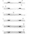
図15(A)及び(B)に示したのは、図1(B)の他の態様である。図15(A)及び(B)において、ゲート線151、ソース線152、第1の遮光層108は図1(B)と共通である。 FIGS. 15A and 15B show another embodiment of FIG. 15A and 15B, the
図1(B)では第2の遮光層109及びコンタクトホール103がドレイン電極より小さい形状を示したが、図15(A)に示したように、第2の遮光層132がコンタクトホール131を覆い、且つ、一部がドレイン電極と重ならないように形成してもよい。また、図15(B)に示したように、第2の遮光層134の一部及びコンタクトホール133の縁の一部がドレイン電極と重ならないように形成してもよい。 Although the second
また、図15(A)及び(B)と図2(B)とを組み合わせることも可能である。図2(B)では第2の遮光層122及びコンタクトホール153がドレイン電極より小さい形状を示したが、第2の遮光層がコンタクトホールの縁を覆い、且つ、一部がドレイン電極と重ならないように形成してもよい。また、第2の遮光層の一部及びコンタクトホールの縁の一部がドレイン電極と重ならないように形成してもよい。 Further, FIGS. 15A and 15B can be combined with FIG. 2B. In FIG. 2B, the second
同様に、図15(A)及び(B)と図3(B)とを組み合わせることも可能である。図3(B)では着色層(カラーフィルター)を除去する部分の形状がドレイン電極より小さい形状を示したが、着色層(カラーフィルター)を除去する部分の形状コンタクトホールを覆い、且つ、一部がドレイン電極と重ならないように形成してもよい。 Similarly, FIGS. 15A and 15B can be combined with FIG. 3B. In FIG. 3B, the shape of the portion from which the colored layer (color filter) is removed is smaller than that of the drain electrode, but the shape of the portion from which the colored layer (color filter) is removed covers the contact hole and partly May be formed so as not to overlap with the drain electrode.
同様に、図15(A)及び(B)と図4(B)とを組み合わせることも可能である。図4(B)では、着色層(カラーフィルター)を除去する部分の形状がドレイン電極より小さい形状を示したが、着色層(カラーフィルター)を除去する部分の形状がコンタクトホールの縁を覆い、且つ、一部がドレイン電極と重ならないように形成してもよい。また、着色層(カラーフィルター)を除去する部分の形状及びコンタクトホールの縁の一部がドレイン電極と重ならないように形成してもよい。 Similarly, FIGS. 15A and 15B can be combined with FIG. 4B. In FIG. 4B, the shape of the portion from which the colored layer (color filter) is removed is smaller than the drain electrode, but the shape of the portion from which the colored layer (color filter) is removed covers the edge of the contact hole. In addition, it may be formed so that a part thereof does not overlap with the drain electrode. Further, the shape of the portion from which the colored layer (color filter) is removed and a part of the edge of the contact hole may be formed so as not to overlap with the drain electrode.
同様に、図15(A)及び(B)と図5(B)とを組み合わせることも可能である。図5(B)では第2の遮光層309及びコンタクトホール303がドレイン電極より小さい形状を示したが、第2の遮光層がコンタクトホールを覆い、且つ、一部がドレイン電極と重ならないように形成してもよい。また、第2の遮光層の一部及びコンタクトホールの縁の一部がドレイン電極と重ならないように形成してもよい。 Similarly, FIGS. 15A and 15B can be combined with FIG. 5B. In FIG. 5B, the second light-
同様に、図15(A)及び(B)と図6(B)とを組み合わせることも可能である。図6(B)では、第2の遮光層322及びコンタクトホールがドレイン電極より小さい形状を示したが、第2の遮光層がコンタクトホールの縁を覆い、且つ、一部がドレイン電極と重ならないように形成してもよい。また、第2の遮光層の一部及びコンタクトホールの縁の一部がドレイン電極と重ならないように形成してもよい。 Similarly, FIGS. 15A and 15B can be combined with FIG. 6B. In FIG. 6B, the shape of the second
(実施の形態6)
本実施の形態では、本発明を用いた対向基板の作製方法について、図8を用いて説明する。(Embodiment 6)
In this embodiment mode, a method for manufacturing a counter substrate using the present invention will be described with reference to FIGS.
基板500上に遮光層501となる金属クロム膜を成膜する。基板500には、アルミノホウケイ酸ガラス、バリウムホウケイ酸ガラス、石英ガラス等のガラス基板の他、PET(ポリエチレンテレフタレート)、PEN(ポリエチレンナフタレート)、PES(ポリエーテルスルホン)、ポリプロピレンに代表されるプラスチックや、アクリルなどに代表される合成樹脂を原料とする基板を用いることができる。金属クロム膜の成膜方法としては、スパッタリング法等を用いるとよい。続いて、フォトリソグラフィー法により所望の形状に加工することによって、遮光層501を形成する(図8(A))。 A metal chromium film to be the
なお、遮光層の材料としては、遮光性の膜(例えば、クロム(Cr)の単層膜、酸化クロム(CrxOy)とクロム(Cr)の積層膜、カーボンブラックなどの顔料、染料等を分散させた樹脂膜等)を用いることができる。また、RGBそれぞれのカラーフィルターを重ねて遮光層として用いてもよい。The material of the light shielding layer includes a light shielding film (for example, a single layer film of chromium (Cr), a laminated film of chromium oxide (Crx Oy ) and chromium (Cr), a pigment such as carbon black, a dye, etc. Or the like can be used. In addition, RGB color filters may be stacked to be used as a light shielding layer.
このとき、図1に示した構成とするには、アクティブマトリクス基板のゲート線151及びソース線152に対応する領域と、薄膜トランジスタのソース領域又はドレイン領域のコンタクトホール103に対応する領域に遮光層を形成する。図2に示した構成とするには、アクティブマトリクス基板のゲート線151及びソース線152に対応する領域と、薄膜トランジスタのソース領域又はドレイン領域のコンタクトホール153のうち絶縁膜102が傾斜している部分121(コンタクトホールの縁)に対応する領域に遮光層を形成する。図3及び図4に示した構成とするには、アクティブマトリクス基板のゲート線251及びソース線252に対応する領域に遮光層を形成する。図5に示した構成とするには、アクティブマトリクス基板のゲート線351及びソース線352に対応する領域と、薄膜トランジスタのソース領域又はドレイン領域のコンタクトホール303に対応する領域に遮光層を形成する。図6に示した構成とするには、アクティブマトリクス基板のゲート線351及びソース線352に対応する領域と、薄膜トランジスタのソース領域又はドレイン領域のコンタクトホールのうち絶縁膜302が傾斜している部分321(コンタクトホールの縁)に対応する領域に遮光層を形成する。 At this time, in order to obtain the structure shown in FIG. 1, a light shielding layer is formed in a region corresponding to the
次に、着色層(カラーフィルター)を形成する。カラーフィルターの形成方法には、顔料分散法、染色法、電着法、印刷法などがあり、どの方法を用いてもよい。本実施の形態では顔料分散法を用いた場合について説明する。 Next, a colored layer (color filter) is formed. The color filter forming method includes a pigment dispersion method, a dyeing method, an electrodeposition method, a printing method, and the like, and any method may be used. In this embodiment, a case where a pigment dispersion method is used will be described.
顔料分散法には、エッチング法とカラーレジスト法の2つがある。エッチング法を用いた場合、遮光層が形成された基板上に、まずRの顔料を分散した着色樹脂をスピンコート法などによって塗布し、乾燥、予備加熱する。続いて、ポジレジストを塗布した後にマスク露光を行う。続いて、アルカリ水溶液でポジレジストの現像と着色樹脂膜のエッチングを行い、有機溶剤によってポジレジストを剥離することによって、Rの着色樹脂膜502を形成することができる(図8(B))。 There are two pigment dispersion methods: an etching method and a color resist method. When the etching method is used, a colored resin in which an R pigment is dispersed is first applied onto a substrate on which a light shielding layer is formed by a spin coating method or the like, followed by drying and preheating. Subsequently, mask exposure is performed after applying a positive resist. Subsequently, the positive resist is developed with an alkaline aqueous solution and the colored resin film is etched, and the positive resist is peeled off with an organic solvent, whereby the R
GとBの着色樹脂についても同じ工程を繰り返し、Gの着色樹脂膜503及びBの着色樹脂膜504を形成する(図8(C)〜(D))。続いて、保護膜を塗布する(図示せず)。以上の工程によって、カラーフィルターが形成される。 The same process is repeated for the G and B colored resins to form the G colored
カラーレジスト法を用いた場合(図示せず)、着色樹脂にレジストのような光硬化性を持たせたカラーレジストを用いる。カラーレジストとは、顔料をアクリル・エポキシ系の紫外線硬化樹脂(ネガレジスト)などに分散し、溶媒に溶かしたものである。遮光層を形成した基板上にカラーレジスト(R)をスピンコート法などによって塗布する。次に、マスクを介して露光し、現像することによって、所望の形状に加工する。 When a color resist method is used (not shown), a color resist in which a colored resin has photocurability such as a resist is used. The color resist is obtained by dispersing a pigment in an acrylic / epoxy ultraviolet curable resin (negative resist) or the like and dissolving it in a solvent. A color resist (R) is applied by spin coating or the like on the substrate on which the light shielding layer is formed. Next, it is processed into a desired shape by exposing through a mask and developing.
G及びBのカラーレジストについても同じ工程を繰り返し、保護膜を塗布する。以上の工程によって、着色層(カラーフィルター)が形成される。 The same process is repeated for the G and B color resists, and a protective film is applied. Through the above steps, a colored layer (color filter) is formed.
このとき、図1及び図2に示した構成とする場合には、特に着色層(カラーフィルター)を除去する必要はない。図3及び図5に示した構成とするには、アクティブマトリクス基板上の薄膜トランジスタのソース領域又はドレイン領域のコンタクトホールに対応する領域の着色層を除去する。図4及び図6に示した構成とするには、アクティブマトリクス基板上の薄膜トランジスタのソース領域又はドレイン領域のコンタクトホールのうち絶縁膜が傾斜している領域(コンタクトホールの縁)に対応する領域の着色層(カラーフィルター)を除去する。 At this time, when the configuration shown in FIGS. 1 and 2 is used, it is not particularly necessary to remove the colored layer (color filter). In the structure shown in FIGS. 3 and 5, the colored layer in the region corresponding to the contact hole in the source region or the drain region of the thin film transistor on the active matrix substrate is removed. 4 and 6, the region corresponding to the region (edge of the contact hole) in which the insulating film is inclined among the contact holes of the source region or the drain region of the thin film transistor on the active matrix substrate. The colored layer (color filter) is removed.
次に、対向電極505を形成する(図8(E))。対向電極505には、酸化インジウムに酸化スズを混合したインジウムスズ酸化物(ITO)、インジウムスズ酸化物(ITO)に酸化珪素を混合したインジウムスズ珪素酸化物(ITSO)、酸化インジウムに酸化亜鉛を混合したインジウム亜鉛酸化物(IZO)、酸化亜鉛(ZnO)、または酸化スズ(SnO2)等を用いることができる。成膜方法としては、真空蒸着法やスパッタリング法等があげられる。Next, the
続いて、配向膜として機能する絶縁膜506を形成する(図8(F))。絶縁膜506は、ポリイミドやポリビニルアルコール等の高分子化合物膜を印刷法、ロールコート法等で形成した後、ラビングすることにより形成することができる。また、酸化珪素を基板に対して斜めから蒸着して形成することもできる。また、光反応型の高分子化合物に偏光したUV光を照射し、光反応型の高分子化合物を重合させて形成することもできる。ここでは、ポリイミドやポリビニルアルコール等の高分子化合物膜を印刷法により印刷し、焼成した後、ラビングすることで形成する。 Subsequently, an insulating
以上の工程により、選択的に遮光層を形成した対向基板を作製することができる。 Through the above steps, a counter substrate on which a light shielding layer is selectively formed can be manufactured.
本実施の形態は、実施の形態1〜4と自由に組み合わせることができる。 This embodiment mode can be freely combined with Embodiment Modes 1 to 4.
(実施の形態7)
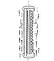
本実施の形態では、本発明の液晶表示装置の構成について、図10を用いて説明する。図10(A)は、アクティブマトリクス基板701と対向基板702との間に液晶層を挟んでなる液晶パネルの上面図であり、図10(B)は、図10(A)のG−G’の断面図に相当する。また、アクティブマトリクス基板701としては、どのように形成されたものを用いてもよく、対向基板702としては、実施の形態1〜4で説明したものを用いることとする。ここでは、実施の形態2に示した対向基板を図示した。(Embodiment 7)
In this embodiment mode, a structure of a liquid crystal display device of the present invention is described with reference to FIG. FIG. 10A is a top view of a liquid crystal panel in which a liquid crystal layer is sandwiched between an
図10(A)において、705は画素部、706は駆動回路部である。本実施の形態において、画素部705は、シール材703で囲まれた領域内に形成され、駆動回路部706は、その領域外に実装されている。 In FIG. 10A, reference numeral 705 denotes a pixel portion and 706 denotes a driver circuit portion. In this embodiment mode, the pixel portion 705 is formed in a region surrounded by the sealant 703, and the driver circuit portion 706 is mounted outside the region.
また、アクティブマトリクス基板701と対向基板702とを封止するシール材703には、密閉空間の間隔を保持するためのギャップ材が含有されており、これらにより形成された空間には、液晶が充填されている。なお、図10(A)には、アクティブマトリクス基板701と対向基板702とをシール材703によって貼り合わせた後、両基板の間に液晶を注入し、封止材704によって封止する場合について示したが、本発明はこの方法に限られることはなく、アクティブマトリクス基板701と対向基板702のうちの一方の基板上に液晶を滴下した後、両方の基板を貼り合わせる方法(ODF法)を用いることもできる。 In addition, the sealing material 703 that seals the
次に、断面構造について、図10(B)を用いて説明する。アクティブマトリクス基板701を形成する第1の基板707上には画素部705が形成されており、TFTを代表とする半導体素子を複数有している。また、本実施の形態では、基板上に実装された駆動回路部706には、ソース線駆動回路およびゲート線駆動回路が含まれている。 Next, a cross-sectional structure is described with reference to FIG. A pixel portion 705 is formed over a first substrate 707 on which an
画素部705には、複数の画素が形成されており、画素電極である第1の電極711は、TFT713と電気的に接続されている。 A plurality of pixels are formed in the pixel portion 705, and the
一方、対向基板702を形成する第2の基板708上には、第1の遮光層716、第2の遮光層717、第2の電極719が形成されている。また、第2の電極719上には、配向膜720が形成されている。 On the other hand, a first light-
また、第2の遮光層717は、アクティブマトリクス基板701に形成されたコンタクトホールに対応する領域に設けられている。 The second
なお、本実施の形態で示す液晶表示装置において、アクティブマトリクス基板701上に形成された第1の電極711と、対向基板702上に形成された第2の電極719との間に液晶層712を挟んでなる部分が液晶素子である。 Note that in the liquid crystal display device described in this embodiment, a
また、721は柱状スペーサーであり、アクティブマトリクス基板701と対向基板702との間の距離(セルギャップ)を制御するために設けられている。柱状スペーサー721は絶縁膜を所望の形状にエッチングして形成されている。なお、球状スペーサーを用いてもよい。 A
画素部705、および駆動回路部706に与えられる各種信号及び電位は、接続配線722を介して、FPC723から供給されている。なお、接続配線722とFPC723とは、異方性導電膜又は異方性導電樹脂724で電気的に接続されている。なお、異方性導電膜又は異方性導電樹脂の代わりにハンダや銀ペースト等の導電性ペーストを用いてもよい。 Various signals and potentials supplied to the pixel portion 705 and the driver circuit portion 706 are supplied from the
また、図示しないが、アクティブマトリクス基板701及び対向基板702の一方又は両方の表面には、接着剤によって偏光板が固定されている。なお、偏光板の他に位相差板を設けても良い。 Although not shown, a polarizing plate is fixed to one or both surfaces of the
(実施の形態8)
本実施の形態では、本発明の液晶表示装置における駆動回路の実装方法について、図11を用いて説明する。(Embodiment 8)
In this embodiment mode, a method for mounting a driver circuit in the liquid crystal display device of the present invention is described with reference to FIGS.
図11(A)の場合には、画素部801の周辺にソース線駆動回路802、及びゲート線駆動回路803a、803bが実装される。すなわち、公知の異方性導電接着剤、及び異方性導電フィルムを用いた実装方法、COG方式、ワイヤボンディング方法、並びにハンダバンプを用いたリフロー処理等により、基板800上にICチップ805を実装することで、ソース線駆動回路802、及びゲート線駆動回路803a、803b等が実装される。なお、ICチップ805は、FPC(フレキシブルプリントサーキット)806を介して、外部回路と接続される。 In the case of FIG. 11A, a source
なお、ソース線駆動回路802の一部、例えばアナログスイッチを基板上に形成し、かつその他の部分を別途ICチップで実装してもよい。 Note that a part of the source
また、図11(B)の場合には、画素部801とゲート線駆動回路803a、803b等が基板上に形成され、ソース線駆動回路802等が別途ICチップで実装される。すなわち、COG方式などの実装方法により、画素部801とゲート線駆動回路803a、803b等が形成された基板800上にICチップ805を実装することで、ソース線駆動回路802等が実装される。なお、ICチップ805は、FPC806を介して外部回路を接続される。 In the case of FIG. 11B, a
なお、ソース線駆動回路802の一部、例えばアナログスイッチを基板上に形成し、かつその他の部分を別途ICチップで実装してもよい。 Note that a part of the source
さらに、図11(C)の場合には、TAB方式によりソース線駆動回路802等が実装される。なお、ICチップ805は、FPC806を介して、外部回路と接続される。図11(C)では、ソース線駆動回路802等をTAB方式により実装しているが、ゲート線駆動回路等をTAB方式により実装してもよい。 Further, in the case of FIG. 11C, the source
ICチップ805をTAB方式により実装すると、基板に対して画素部を大きく設けることができ、狭額縁化を達成することができる。 When the
また、ICチップ805の代わりにガラス基板上にICを形成したIC(以下、ドライバICと表記する)を設けても良い。ICチップ805は、円形のシリコンウェハからICチップを取り出すため、母体基板形状に制約がある。一方、ドライバICは、母体基板がガラスであり、形状に制約がないため、生産性を高めることができる。そのため、ドライバICの形状寸法は自由に設定することができる。例えば、ドライバICの長辺の長さを15〜80mmとして形成すると、ICチップを実装する場合と比較し、必要な数を減らすことができる。その結果、接続端子数を低減することができ、製造上の歩留まりを向上させることができる。 Further, instead of the
ドライバICは、基板上に形成された結晶質半導体を用いて形成することができ、結晶質半導体は連続発振型のレーザー光を照射することで形成するとよい。連続発振型のレーザー光を照射して得られる半導体膜は、結晶欠陥が少なく、大粒径の結晶粒を有する。その結果、このような半導体膜を有するトランジスタは、移動度や応答速度が良好となり、高速駆動が可能となり、ドライバICに好適である。 The driver IC can be formed using a crystalline semiconductor formed over a substrate, and the crystalline semiconductor is preferably formed by irradiation with continuous wave laser light. A semiconductor film obtained by irradiating continuous wave laser light has few crystal defects and large crystal grains. As a result, a transistor having such a semiconductor film has favorable mobility and response speed, can be driven at high speed, and is suitable for a driver IC.
(実施の形態9)
本実施の形態では、実施の形態1〜7を実施することにより形成される本発明の液晶表示装置に電源回路、コントローラ等の外部回路を接続して形成される液晶モジュールであって、白色ライトを用いてカラー表示をする液晶モジュールについて、図12の断面図を用いて説明する。(Embodiment 9)
In the present embodiment, a liquid crystal module formed by connecting an external circuit such as a power supply circuit and a controller to the liquid crystal display device of the present invention formed by carrying out the first to seventh embodiments, the white light A liquid crystal module that performs color display using the above will be described with reference to a cross-sectional view of FIG.
図12に示すように、アクティブマトリクス基板901と対向基板902は、シール材903により固着され、それらの間には液晶層905が設けられ、液晶表示パネルが形成されている。 As shown in FIG. 12, the
また、アクティブマトリクス基板901上に形成された着色膜906は、カラー表示を行う場合に必要であり、RGB方式の場合は、赤、緑、青の各色に対応した着色膜が各画素に対応して設けられている。アクティブマトリクス基板901と対向基板902との内側には、配向膜918、919が形成されている。また、アクティブマトリクス基板901と対向基板902との外側には、偏光板907、908が配設されている。また、偏光板907の表面には、保護膜909が形成されており、外部からの衝撃を緩和している。 The colored film 906 formed on the
アクティブマトリクス基板901に設けられた接続端子910には、FPC911を介して配線基板912が接続されている。配線基板912には、画素駆動回路(ICチップ、ドライバIC等)、コントロール回路や電源回路などの外部回路913が組み込まれている。 A
冷陰極管914、反射板915、及び光学フィルム916、インバーター(図示せず)は、バックライトユニットであり、これらが光源となって液晶表示パネルへ光を投射する。液晶表示パネル、光源、配線基板912、FPC911等は、ベゼル917で保持及び保護されている。 The cold cathode tube 914, the reflector 915, the
(実施の形態10)
本発明の液晶表示装置を備えた電子機器として、テレビジョン装置(単にテレビ、又はテレビジョン受信機ともよぶ)、デジタルカメラ、デジタルビデオカメラ、電話装置(単に電話機、電話ともよぶ)、PDA等の情報端末、電子ブック、ゲーム機、コンピューター用のモニター、コンピューター、カーオーディオやMP3プレーヤー等の音響再生装置、家庭用ゲーム機等の記録媒体を備えた画像再生装置等が挙げられる。その好ましい形態について、図13を参照して説明する。(Embodiment 10)
As an electronic apparatus including the liquid crystal display device of the present invention, a television device (also simply referred to as a television or a television receiver), a digital camera, a digital video camera, a telephone device (also simply referred to as a telephone or a telephone), a PDA, or the like Examples thereof include information terminals, electronic books, game machines, computer monitors, computers, sound playback devices such as car audio and MP3 players, and image playback devices equipped with recording media such as home game machines. The preferable form is demonstrated with reference to FIG.
図13(A)に示すテレビジョン装置は、本体8001、表示部8002等を含んでいる。表示部8002には、本発明の液晶表示装置を適用することができる。本発明の液晶表示装置は、視認性の高い画像表示が実現可能なテレビジョン装置を提供することができる。 A television device illustrated in FIG. 13A includes a main body 8001, a
図13(B)に示す情報端末機器は、本体8101、表示部8102等を含んでいる。表示部8102には、本発明の液晶表示装置を適用することができる。本発明の液晶表示装置は、視認性の高い画像表示が実現可能な情報端末機器を提供することができる。 An information terminal device illustrated in FIG. 13B includes a
図13(C)に示すデジタルビデオカメラは、本体8201、表示部8202等を含んでいる。表示部8202には、本発明の液晶表示装置を適用することができる。本発明の液晶表示装置は、視認性の高い画像表示が実現可能なデジタルビデオカメラを提供することができる。 A digital video camera shown in FIG. 13C includes a
図13(D)に示す電話機は、本体8301、表示部8302等を含んでいる。表示部8302には、本発明の液晶表示装置を適用することができる。本発明の液晶表示装置は、視認性の高い画像表示が実現可能な電話機を提供することができる。 A telephone shown in FIG. 13D includes a
図13(E)に示すモニターは、本体8401、表示部8402等を含んでいる。表示部8402には、本発明の液晶表示装置を適用することができる。本発明の液晶表示装置は、視認性の高い画像表示が実現可能なモニターを提供することができる。 A monitor illustrated in FIG. 13E includes a
(実施の形態11)
実施の形態1〜10では、液晶表示装置について説明してきたが、本発明は、液晶表示装置だけでなく、発光装置に用いることも可能である。発光装置において、コンタクトホール部で発光させる場合、コンタクトホール部とそれ以外の部分とで光の通る光路長が異なるため、色むらが発生する。(Embodiment 11)
Although the liquid crystal display device has been described in Embodiments 1 to 10, the present invention can be used not only for a liquid crystal display device but also for a light emitting device. In the light emitting device, when light is emitted from the contact hole portion, the optical path length through which the contact hole portion and the other portion pass is different, and thus color unevenness occurs.
図14において、1000は基板、1001は薄膜トランジスタ、1002は絶縁膜、1003はコンタクトホール、1004は第1の電極、1005aはソース電極、1005bはドレイン電極、1006は発光層を含む層、1007は第2の電極、1008は基板、1009は遮光層、1010は空間である。 In FIG. 14,
図14に示したように、液晶表示装置の場合と同様に、発光装置のコンタクトホール1003に対応する領域に遮光層を形成すると、色むらのない画像表示となる。 As shown in FIG. 14, when a light shielding layer is formed in a region corresponding to the
なお、図14では、実施の形態2に示した構成を適用した発光装置を示しているが、発光装置に実施の形態1〜5のいずれの形態を適用することが可能である。また、実施の形態10の表示部に発光装置を用いることも可能である。 Note that FIG. 14 illustrates a light-emitting device to which the structure described in Embodiment 2 is applied; however, any one of Embodiments 1 to 5 can be applied to the light-emitting device. In addition, a light-emitting device can be used for the display portion in Embodiment Mode 10.
100 基板
101 薄膜トランジスタ
102 絶縁膜
103 コンタクトホール
104 画素電極
105a ソース電極
105b ドレイン電極
106 配向膜
107 基板
108 第1の遮光層
109 第2の遮光層
110 対向電極
111 配向膜
112 液晶層
121 絶縁膜が傾斜している部分
122 第2の遮光層
131 コンタクトホール
132 第2の遮光層
133 コンタクトホール
134 第2の遮光層
151 ゲート線
152 ソース線
153 コンタクトホール
154 半導体層
200 基板
201 薄膜トランジスタ
202 絶縁膜
203 コンタクトホール
204 画素電極
205a ソース電極
205b ドレイン電極
206 配向膜
207 基板
208 遮光層
209 着色層(カラーフィルター)
210 対向電極
211 配向膜
212 液晶層
221 絶縁膜が傾斜している部分
222 第2の着色層(カラーフィルター)
223 第1の着色層(カラーフィルター)
251 ゲート線
252 ソース線
253 コンタクトホール
254 半導体層
300 基板
301 薄膜トランジスタ
302 絶縁膜
303 コンタクトホール
304 画素電極
305a ソース電極
305b ドレイン電極
306 配向膜
307 基板
308 第1の遮光層
309 第2の遮光層
310 着色層(カラーフィルター)
311 対向電極
312 配向膜
313 液晶層
321 絶縁膜が傾斜している部分
322 第2の遮光層
323 第1の着色層(カラーフィルター)
324 第2の着色層(カラーフィルター)
351 ゲート線
352 ソース線
354 半導体層
401 第1の遮光層
402 第2の遮光層
500 基板
501 遮光層
502 Rの着色樹脂
503 Gの着色樹脂
504 Bの着色樹脂
505 対向電極
506 絶縁膜
601 ソース電極又はドレイン電極
602 画素電極
611 ソース電極又はドレイン電極
612 画素電極
613 導電層
621 ソース領域又はドレイン領域
622 画素電極
631 ソース領域又はドレイン領域
632 画素電極
633 導電層
701 アクティブマトリクス基板
702 対向基板
703 シール材
704 封止材
705 画素部
706 駆動回路部
707 第1の基板
708 第2の基板
710 液晶素子
711 第1の電極
712 液晶層
713 TFT
716 第1の遮光層
717 第2の遮光層
719 第2の電極
720 配向膜
721 柱状スペーサー
722 接続配線
723 FPC
724 異方性導電樹脂
800 基板
801 画素部
802 ソース線駆動回路
803a ゲート線駆動回路
803b ゲート線駆動回路
805 ICチップ
806 FPC
901 アクティブマトリクス基板
902 対向基板
903 シール材
905 液晶層
906 着色膜
907 偏光板
909 保護膜
910 接続端子
911 FPC
912 配線基板
913 外部回路
914 冷陰極管
915 反射板
916 光学フィルム
917 ベゼル
918 配向膜
1000 基板
1001 薄膜トランジスタ
1002 絶縁膜
1003 コンタクトホール
1004 第1の電極
1005a ソース電極
1005b ドレイン電極
1006 発光層を含む層
1007 第2の電極
1008 基板
1009 遮光層
1010 空間
8001 本体
8002 表示部
8101 本体
8102 表示部
8201 本体
8202 表示部
8301 本体
8302 表示部
8401 本体
8402 表示部DESCRIPTION OF
210
223 First colored layer (color filter)
311
324 Second colored layer (color filter)
716 1st
724 Anisotropic
901 Active matrix substrate 902 Counter substrate 903 Sealing material 905 Liquid crystal layer 906 Colored film 907 Polarizing plate 909 Protective film 910
912
Claims (8)
Translated fromJapanese前記第1の基板と対向する第2の基板と、を有し、
前記第1の基板は、
薄膜トランジスタと、
前記薄膜トランジスタと電気的に接続した導電層と、
前記導電層上に設けられ、コンタクトホールを有する絶縁膜と、
前記導電層及び前記コンタクトホールを有する絶縁膜上に設けられ、前記コンタクトホールを介して前記導電層と電気的に接続した画素電極と、を有し、
前記第2の基板は、
ゲート線及びソース線を覆う第1の遮光層と、
前記第1の遮光層と独立して設けられた第2の遮光層と、を有し、
前記第2の遮光層は、開口部を有し、
前記第2の遮光層は、前記コンタクトホールの縁と重なる領域に設けられることを特徴とする液晶表示装置。A first substrate;
A second substrate facing the first substrate,
The first substrate is
A thin film transistor;
A conductive layer electrically connected to the thin film transistor;
An insulating film provided on the conductive layer and having a contact hole;
A pixel electrode provided on the insulating film having the conductive layer and the contact hole, and electrically connected to the conductive layer through the contact hole;
The second substrate is
A first light-shielding layer covering the gate line and the source line;
Anda second light-shielding layer provided independently of the first light-shielding layer,
The second light shielding layer has an opening,
It said second light-shielding layeris a liquid crystal display device, characterized in that provided in a region overlapping the edge of thefront SL contact hole.
前記第1の基板と対向する第2の基板と、を有し、
前記第1の基板は、
薄膜トランジスタと、
前記薄膜トランジスタと電気的に接続した導電層と、
前記導電層上に設けられ、コンタクトホールを有する絶縁膜と、
前記導電層及び前記コンタクトホールを有する絶縁膜上に設けられ、前記コンタクトホールを介して前記導電層と電気的に接続した画素電極と、を有し、
前記第2の基板は、
第1の開口部を有する着色層と、
ゲート線及びソース線を覆う第1の遮光層と、
前記第1の遮光層と独立して設けられた第2の遮光層と、を有し、
前記第2の遮光層は、第2の開口部を有し、
前記第2の遮光層は、前記コンタクトホールの縁と重なる領域に設けられ、
前記第1の開口部は、少なくとも前記コンタクトホールの縁と重なる領域に設けられることを特徴とする液晶表示装置。A first substrate;
A second substrate facing the first substrate,
The first substrate is
A thin film transistor;
A conductive layer electrically connected to the thin film transistor;
An insulating film provided on the conductive layer and having a contact hole;
The conductive layer and provided on an insulating film having the contact hole,having a pixel electrode connected to the conductive layer and the electrically throughthe contacthole,
The second substrate is
A colored layer having afirst opening;
A first light-shielding layer covering the gate line and the source line;
Anda second light-shielding layer provided independently of the first light-shielding layer,
The second light shielding layer has a second opening,
It said second light-shielding layeris provided in a region overlapping the edge of thefront SL contact hole,
Before SLfirst opening, a liquid crystal display device, characterized in that provided in a region that overlaps with the edge of at least the contact hole.
前記第1の基板と対向する第2の基板と、を有し、A second substrate facing the first substrate,
前記第1の基板は、The first substrate is
薄膜トランジスタと、A thin film transistor;
前記薄膜トランジスタと電気的に接続した導電層と、A conductive layer electrically connected to the thin film transistor;
前記導電層上に設けられ、コンタクトホールを有する絶縁膜と、An insulating film provided on the conductive layer and having a contact hole;
前記導電層及び前記コンタクトホールを有する絶縁膜上に設けられ、前記コンタクトホールを介して前記導電層と電気的に接続した画素電極と、を有し、A pixel electrode provided on the insulating film having the conductive layer and the contact hole, and electrically connected to the conductive layer through the contact hole;
前記第2の基板は、The second substrate is
第1の開口部を有する第1の着色層と、A first colored layer having a first opening;
前記第1の開口部内に設けられた第2の着色層と、A second colored layer provided in the first opening;
ゲート線及びソース線を覆う第1の遮光層と、A first light-shielding layer covering the gate line and the source line;
前記第1の遮光層と独立して設けられた第2の遮光層と、を有し、A second light shielding layer provided independently of the first light shielding layer,
前記第2の遮光層は、第2の開口部を有し、The second light shielding layer has a second opening,
前記第2の遮光層は、前記コンタクトホールの縁と重なる領域に設けられ、The second light shielding layer is provided in a region overlapping with an edge of the contact hole;
前記第1の開口部は、少なくとも前記コンタクトホールの縁と重なる領域に設けられることを特徴とする液晶表示装置。The liquid crystal display device, wherein the first opening is provided at least in a region overlapping with an edge of the contact hole.
前記第2の遮光層と、前記第1の着色層とは重ならず、The second light shielding layer and the first colored layer do not overlap,
前記第2の遮光層と、前記第2の着色層とは重ならないことを特徴とする液晶表示装置。The liquid crystal display device, wherein the second light shielding layer and the second colored layer do not overlap.
前記第1及び第2の遮光層は、顔料もしくは染料を分散させた樹脂膜または遮光性の金属膜であることを特徴とする液晶表示装置。In any one of Claims 1thru | or 4 ,
The liquid crystal display device, wherein the first and second light shielding layers area resin film or a light shielding metal film in which apigment or a dye is dispersed .
前記第2の遮光層は、液晶層を介して前記コンタクトホールの縁と重なる領域に設けられることを特徴とする液晶表示装置。In anyone of Claims1 thru | or 5 ,
The liquid crystal display device, wherein the second light shielding layer is provided in a region overlapping with an edge of the contact hole through a liquid crystal layer.
前記絶縁膜は、樹脂膜であることを特徴とする液晶表示装置。In any one of Claims 1 thru | or 6,
The liquid crystal display device, wherein the insulating film is a resin film.
前記画素電極は、前記絶縁膜を介して前記薄膜トランジスタを覆うように設けられることを特徴とする液晶表示装置。
In any one of Claims 1 thru | or 7,
The liquid crystal display device, wherein the pixel electrode is provided so as to cover the thin film transistor with the insulating film interposed therebetween.
Priority Applications (1)
| Application Number | Priority Date | Filing Date | Title |
|---|---|---|---|
| JP2007321022AJP5258277B2 (en) | 2006-12-26 | 2007-12-12 | Liquid crystal display |
Applications Claiming Priority (3)
| Application Number | Priority Date | Filing Date | Title |
|---|---|---|---|
| JP2006350137 | 2006-12-26 | ||
| JP2006350137 | 2006-12-26 | ||
| JP2007321022AJP5258277B2 (en) | 2006-12-26 | 2007-12-12 | Liquid crystal display |
Related Child Applications (1)
| Application Number | Title | Priority Date | Filing Date |
|---|---|---|---|
| JP2013090269ADivisionJP5542990B2 (en) | 2006-12-26 | 2013-04-23 | Liquid crystal display |
Publications (2)
| Publication Number | Publication Date |
|---|---|
| JP2008181099A JP2008181099A (en) | 2008-08-07 |
| JP5258277B2true JP5258277B2 (en) | 2013-08-07 |
Family
ID=39542250
Family Applications (13)
| Application Number | Title | Priority Date | Filing Date |
|---|---|---|---|
| JP2007321022AActiveJP5258277B2 (en) | 2006-12-26 | 2007-12-12 | Liquid crystal display |
| JP2013090269AActiveJP5542990B2 (en) | 2006-12-26 | 2013-04-23 | Liquid crystal display |
| JP2014008394AActiveJP5619310B2 (en) | 2006-12-26 | 2014-01-21 | Liquid crystal display |
| JP2014186353AActiveJP5923575B2 (en) | 2006-12-26 | 2014-09-12 | Liquid crystal display |
| JP2016077031AActiveJP6130546B2 (en) | 2006-12-26 | 2016-04-07 | Liquid crystal display |
| JP2017079361AActiveJP6429931B2 (en) | 2006-12-26 | 2017-04-13 | Liquid crystal display |
| JP2017171769AActiveJP6250859B2 (en) | 2006-12-26 | 2017-09-07 | Liquid crystal display |
| JP2018203678AWithdrawnJP2019020751A (en) | 2006-12-26 | 2018-10-30 | Liquid crystal display device |
| JP2019085630AActiveJP6591715B2 (en) | 2006-12-26 | 2019-04-26 | Transmission type liquid crystal display device |
| JP2021008800AActiveJP7266623B2 (en) | 2006-12-26 | 2021-01-22 | liquid crystal display |
| JP2023067751AActiveJP7451800B2 (en) | 2006-12-26 | 2023-04-18 | liquid crystal display device |
| JP2024034240AActiveJP7518308B2 (en) | 2006-12-26 | 2024-03-06 | Liquid crystal display device |
| JP2024107973AActiveJP7683096B2 (en) | 2006-12-26 | 2024-07-04 | liquid crystal display device |
Family Applications After (12)
| Application Number | Title | Priority Date | Filing Date |
|---|---|---|---|
| JP2013090269AActiveJP5542990B2 (en) | 2006-12-26 | 2013-04-23 | Liquid crystal display |
| JP2014008394AActiveJP5619310B2 (en) | 2006-12-26 | 2014-01-21 | Liquid crystal display |
| JP2014186353AActiveJP5923575B2 (en) | 2006-12-26 | 2014-09-12 | Liquid crystal display |
| JP2016077031AActiveJP6130546B2 (en) | 2006-12-26 | 2016-04-07 | Liquid crystal display |
| JP2017079361AActiveJP6429931B2 (en) | 2006-12-26 | 2017-04-13 | Liquid crystal display |
| JP2017171769AActiveJP6250859B2 (en) | 2006-12-26 | 2017-09-07 | Liquid crystal display |
| JP2018203678AWithdrawnJP2019020751A (en) | 2006-12-26 | 2018-10-30 | Liquid crystal display device |
| JP2019085630AActiveJP6591715B2 (en) | 2006-12-26 | 2019-04-26 | Transmission type liquid crystal display device |
| JP2021008800AActiveJP7266623B2 (en) | 2006-12-26 | 2021-01-22 | liquid crystal display |
| JP2023067751AActiveJP7451800B2 (en) | 2006-12-26 | 2023-04-18 | liquid crystal display device |
| JP2024034240AActiveJP7518308B2 (en) | 2006-12-26 | 2024-03-06 | Liquid crystal display device |
| JP2024107973AActiveJP7683096B2 (en) | 2006-12-26 | 2024-07-04 | liquid crystal display device |
Country Status (5)
| Country | Link |
|---|---|
| US (2) | US8164718B2 (en) |
| JP (13) | JP5258277B2 (en) |
| KR (3) | KR101439104B1 (en) |
| CN (3) | CN102692777B (en) |
| TW (2) | TWI518413B (en) |
Families Citing this family (21)
| Publication number | Priority date | Publication date | Assignee | Title |
|---|---|---|---|---|
| GB9306301D0 (en) | 1993-03-26 | 1993-05-19 | Boc Group Plc | Freezing apparatus and method |
| CN102113331A (en)* | 2008-07-29 | 2011-06-29 | 汤姆森特许公司 | Display characterization with filtration |
| CN102160103B (en) | 2008-09-19 | 2013-09-11 | 株式会社半导体能源研究所 | Display device |
| KR101711678B1 (en)* | 2009-05-02 | 2017-03-02 | 가부시키가이샤 한도오따이 에네루기 켄큐쇼 | Electronic device |
| US8115883B2 (en) | 2009-08-27 | 2012-02-14 | Semiconductor Energy Laboratory Co., Ltd. | Display device and method for manufacturing the same |
| KR20120068772A (en) | 2009-09-16 | 2012-06-27 | 가부시키가이샤 한도오따이 에네루기 켄큐쇼 | Light-emitting device and manufacturing method thereof |
| US20120236225A1 (en)* | 2009-12-01 | 2012-09-20 | Sharp Kabushiki Kaisha | Display device substrate, manufacturing method of display device substrate, display device, and manufacturing method of display device |
| US8928846B2 (en)* | 2010-05-21 | 2015-01-06 | Semiconductor Energy Laboratory Co., Ltd. | Liquid crystal display device having dielectric film over and in contact with wall-like structures |
| KR101995851B1 (en)* | 2010-07-02 | 2019-07-03 | 가부시키가이샤 한도오따이 에네루기 켄큐쇼 | Semiconductor device |
| WO2012074011A1 (en)* | 2010-12-01 | 2012-06-07 | シャープ株式会社 | Liquid crystal panel and liquid crystal display device |
| KR102082406B1 (en) | 2012-10-05 | 2020-02-28 | 삼성디스플레이 주식회사 | Liquid crystal display |
| CN103913884A (en)* | 2013-06-28 | 2014-07-09 | 上海天马微电子有限公司 | Color film substrate, manufacturing method thereof and display panel |
| CN104349575B (en)* | 2013-07-31 | 2017-12-26 | 鹏鼎控股(深圳)股份有限公司 | Flexible PCB and preparation method thereof |
| JP6159946B2 (en)* | 2013-10-09 | 2017-07-12 | 株式会社Joled | Display device and electronic device |
| TWI534517B (en)* | 2014-01-17 | 2016-05-21 | 群創光電股份有限公司 | Liquid crystal display panel |
| KR102255591B1 (en)* | 2014-11-04 | 2021-05-26 | 엘지디스플레이 주식회사 | Thin Film Transistor Substrate For Flat Panel Display |
| WO2016104185A1 (en)* | 2014-12-26 | 2016-06-30 | シャープ株式会社 | Display device |
| KR102839836B1 (en)* | 2016-11-30 | 2025-07-30 | 엘지디스플레이 주식회사 | Display device |
| CN106647010A (en)* | 2017-03-13 | 2017-05-10 | 惠科股份有限公司 | Display substrate, display panel and display device |
| CN111221188B (en)* | 2020-01-20 | 2022-03-08 | 深圳市华星光电半导体显示技术有限公司 | Display panel |
| CN110161761A (en)* | 2019-05-10 | 2019-08-23 | 香港科技大学 | Liquid crystal display panel and preparation method thereof and display equipment |
Family Cites Families (50)
| Publication number | Priority date | Publication date | Assignee | Title |
|---|---|---|---|---|
| JP3078554B2 (en)* | 1989-11-08 | 2000-08-21 | セイコーエプソン株式会社 | Reflective liquid crystal display |
| DE69332142T2 (en) | 1992-12-25 | 2003-03-06 | Sony Corp., Tokio/Tokyo | Active matrix substrate |
| JP3383047B2 (en)* | 1992-12-25 | 2003-03-04 | ソニー株式会社 | Active matrix substrate |
| JPH07198614A (en)* | 1993-12-28 | 1995-08-01 | Nippon Petrochem Co Ltd | Liquid crystal display device and its defect inspection method |
| JPH08179376A (en)* | 1994-12-22 | 1996-07-12 | Sony Corp | Color display device |
| JPH0943640A (en)* | 1995-07-31 | 1997-02-14 | Sony Corp | Liquid crystal display device |
| JP3587426B2 (en)* | 1996-09-25 | 2004-11-10 | シャープ株式会社 | Liquid crystal display device and method of manufacturing the same |
| TWI236556B (en)* | 1996-10-16 | 2005-07-21 | Seiko Epson Corp | Substrate for a liquid crystal equipment, liquid crystal equipment and projection type display equipment |
| JPH10206889A (en)* | 1997-01-22 | 1998-08-07 | Sharp Corp | Active matrix type liquid crystal display device and manufacturing method thereof |
| JP3738530B2 (en) | 1997-06-30 | 2006-01-25 | ソニー株式会社 | Color display device |
| US7202497B2 (en) | 1997-11-27 | 2007-04-10 | Semiconductor Energy Laboratory Co., Ltd. | Semiconductor device |
| JP3934236B2 (en) | 1998-01-14 | 2007-06-20 | 株式会社半導体エネルギー研究所 | Semiconductor device and manufacturing method thereof |
| JP4202454B2 (en) | 1997-11-27 | 2008-12-24 | 株式会社半導体エネルギー研究所 | Semiconductor device and manufacturing method thereof |
| JP4014710B2 (en) | 1997-11-28 | 2007-11-28 | 株式会社半導体エネルギー研究所 | Liquid crystal display |
| JPH11212115A (en)* | 1998-01-26 | 1999-08-06 | Sharp Corp | Active matrix type liquid crystal display device and manufacturing method thereof |
| JPH11212118A (en)* | 1998-01-27 | 1999-08-06 | Sharp Corp | Active matrix type liquid crystal display device and manufacturing method thereof |
| JP3355143B2 (en)* | 1998-12-22 | 2002-12-09 | 松下電器産業株式会社 | Liquid crystal display device and method of manufacturing the same |
| US6850292B1 (en)* | 1998-12-28 | 2005-02-01 | Seiko Epson Corporation | Electric-optic device, method of fabricating the same, and electronic apparatus |
| JP3187785B2 (en)* | 1999-02-22 | 2001-07-11 | セイコーエプソン株式会社 | Reflective liquid crystal display |
| JP3711781B2 (en)* | 1999-03-12 | 2005-11-02 | セイコーエプソン株式会社 | Electro-optical device and manufacturing method thereof |
| JP3636641B2 (en)* | 1999-08-20 | 2005-04-06 | セイコーエプソン株式会社 | Electro-optic device |
| JP4700156B2 (en)* | 1999-09-27 | 2011-06-15 | 株式会社半導体エネルギー研究所 | Semiconductor device |
| JP3763728B2 (en)* | 1999-09-30 | 2006-04-05 | セイコーエプソン株式会社 | Electro-optical device and projector |
| JP4677654B2 (en) | 2000-04-19 | 2011-04-27 | 日本電気株式会社 | Transmission type liquid crystal display device and manufacturing method thereof |
| JP4599655B2 (en)* | 2000-04-24 | 2010-12-15 | セイコーエプソン株式会社 | Electro-optical device and projector |
| US6542205B2 (en)* | 2000-08-04 | 2003-04-01 | Semiconductor Energy Laboratory Co., Ltd. | Display device |
| KR100720411B1 (en)* | 2000-10-25 | 2007-05-22 | 엘지.필립스 엘시디 주식회사 | Liquid crystal display panel and manufacturing method thereof |
| KR100796481B1 (en)* | 2000-12-29 | 2008-01-21 | 엘지.필립스 엘시디 주식회사 | Liquid crystal display panel and manufacturing method thereof |
| KR100778838B1 (en)* | 2000-12-30 | 2007-11-22 | 엘지.필립스 엘시디 주식회사 | LCD and its manufacturing method |
| JP3729071B2 (en)* | 2001-01-18 | 2005-12-21 | セイコーエプソン株式会社 | Electro-optical device and projector |
| JP4583650B2 (en)* | 2001-04-16 | 2010-11-17 | Nec液晶テクノロジー株式会社 | Color liquid crystal panel, manufacturing method thereof, and color liquid crystal display device |
| KR100820647B1 (en)* | 2001-10-29 | 2008-04-08 | 엘지.필립스 엘시디 주식회사 | Array board for transflective liquid crystal display device and manufacturing method thereof |
| KR20030090079A (en)* | 2002-05-21 | 2003-11-28 | 엘지.필립스 엘시디 주식회사 | Liquid crystal display device |
| JP4029663B2 (en)* | 2002-05-22 | 2008-01-09 | セイコーエプソン株式会社 | Transflective liquid crystal device and electronic device using the same |
| JP2004053828A (en)* | 2002-07-18 | 2004-02-19 | Alps Electric Co Ltd | Active matrix display device |
| KR100884541B1 (en)* | 2002-12-10 | 2009-02-18 | 엘지디스플레이 주식회사 | LCD and its manufacturing method |
| KR100475637B1 (en)* | 2002-12-20 | 2005-03-10 | 엘지.필립스 엘시디 주식회사 | Reflective type Liquid Crystal Display Device and Method for Manufacturing the same |
| JP4417072B2 (en)* | 2003-03-28 | 2010-02-17 | シャープ株式会社 | Substrate for liquid crystal display device and liquid crystal display device using the same |
| KR100940909B1 (en)* | 2003-06-10 | 2010-02-08 | 엘지디스플레이 주식회사 | Reflective type liquid crystal display device |
| JP2005062759A (en)* | 2003-08-20 | 2005-03-10 | Seiko Epson Corp | Substrate device, and electro-optical device and electronic apparatus provided with the same |
| JP4419119B2 (en)* | 2003-12-03 | 2010-02-24 | 日本電気株式会社 | Electro-optical device and projection display device |
| JP2005292223A (en)* | 2004-03-31 | 2005-10-20 | Seiko Epson Corp | Electro-optical device and electronic apparatus |
| JP4605438B2 (en)* | 2004-04-09 | 2011-01-05 | ソニー株式会社 | Liquid crystal display device and manufacturing method thereof |
| JP4041821B2 (en)* | 2004-04-23 | 2008-02-06 | シャープ株式会社 | Liquid crystal display |
| JP4016977B2 (en)* | 2004-09-03 | 2007-12-05 | セイコーエプソン株式会社 | Liquid crystal display device, electronic equipment |
| JP2006227295A (en)* | 2005-02-17 | 2006-08-31 | Toppan Printing Co Ltd | Color filter, color filter substrate, and liquid crystal display device using the same |
| KR20060115778A (en)* | 2005-05-06 | 2006-11-10 | 삼성전자주식회사 | Thin film transistor substrate, liquid crystal display including the same and manufacturing method thereof |
| JP4179327B2 (en) | 2006-01-31 | 2008-11-12 | エプソンイメージングデバイス株式会社 | LCD panel |
| CN1970130B (en)* | 2006-10-27 | 2011-05-25 | 威海戥同测试设备有限公司 | Liquid and liquid separation device |
| JP2008116528A (en)* | 2006-11-01 | 2008-05-22 | Epson Imaging Devices Corp | Liquid crystal display panel |
- 2007
- 2007-12-12JPJP2007321022Apatent/JP5258277B2/enactiveActive
- 2007-12-13USUS11/955,602patent/US8164718B2/enactiveActive
- 2007-12-25TWTW103128088Apatent/TWI518413B/enactive
- 2007-12-25TWTW096149953Apatent/TWI518407B/enactive
- 2007-12-26KRKR1020070137217Apatent/KR101439104B1/enactiveActive
- 2007-12-26CNCN201210201263.XApatent/CN102692777B/enactiveActive
- 2007-12-26CNCN2007101943972Apatent/CN101211082B/enactiveActive
- 2007-12-26CNCN201510024649.1Apatent/CN104536230B/enactiveActive
- 2012
- 2012-04-19USUS13/450,572patent/US8400590B2/enactiveActive
- 2013
- 2013-04-23JPJP2013090269Apatent/JP5542990B2/enactiveActive
- 2014
- 2014-01-21JPJP2014008394Apatent/JP5619310B2/enactiveActive
- 2014-02-27KRKR1020140023587Apatent/KR101549424B1/enactiveActive
- 2014-08-20KRKR1020140108268Apatent/KR101542362B1/enactiveActive
- 2014-09-12JPJP2014186353Apatent/JP5923575B2/enactiveActive
- 2016
- 2016-04-07JPJP2016077031Apatent/JP6130546B2/enactiveActive
- 2017
- 2017-04-13JPJP2017079361Apatent/JP6429931B2/enactiveActive
- 2017-09-07JPJP2017171769Apatent/JP6250859B2/enactiveActive
- 2018
- 2018-10-30JPJP2018203678Apatent/JP2019020751A/ennot_activeWithdrawn
- 2019
- 2019-04-26JPJP2019085630Apatent/JP6591715B2/enactiveActive
- 2021
- 2021-01-22JPJP2021008800Apatent/JP7266623B2/enactiveActive
- 2023
- 2023-04-18JPJP2023067751Apatent/JP7451800B2/enactiveActive
- 2024
- 2024-03-06JPJP2024034240Apatent/JP7518308B2/enactiveActive
- 2024-07-04JPJP2024107973Apatent/JP7683096B2/enactiveActive
Also Published As
Similar Documents
| Publication | Publication Date | Title |
|---|---|---|
| JP6591715B2 (en) | Transmission type liquid crystal display device | |
| US7872724B2 (en) | Color filter substrate and liquid crystal display panel comprising the same | |
| US20110222015A1 (en) | Liquid crystal display | |
| KR20060019405A (en) | Display substrate, alignment film forming method and display device having same |
Legal Events
| Date | Code | Title | Description |
|---|---|---|---|
| A621 | Written request for application examination | Free format text:JAPANESE INTERMEDIATE CODE: A621 Effective date:20101129 | |
| A977 | Report on retrieval | Free format text:JAPANESE INTERMEDIATE CODE: A971007 Effective date:20120523 | |
| A131 | Notification of reasons for refusal | Free format text:JAPANESE INTERMEDIATE CODE: A131 Effective date:20120626 | |
| A521 | Request for written amendment filed | Free format text:JAPANESE INTERMEDIATE CODE: A523 Effective date:20120716 | |
| TRDD | Decision of grant or rejection written | ||
| A01 | Written decision to grant a patent or to grant a registration (utility model) | Free format text:JAPANESE INTERMEDIATE CODE: A01 Effective date:20130326 | |
| A61 | First payment of annual fees (during grant procedure) | Free format text:JAPANESE INTERMEDIATE CODE: A61 Effective date:20130423 | |
| FPAY | Renewal fee payment (event date is renewal date of database) | Free format text:PAYMENT UNTIL: 20160502 Year of fee payment:3 | |
| R150 | Certificate of patent or registration of utility model | Ref document number:5258277 Country of ref document:JP Free format text:JAPANESE INTERMEDIATE CODE: R150 Free format text:JAPANESE INTERMEDIATE CODE: R150 | |
| R250 | Receipt of annual fees | Free format text:JAPANESE INTERMEDIATE CODE: R250 | |
| R250 | Receipt of annual fees | Free format text:JAPANESE INTERMEDIATE CODE: R250 | |
| R250 | Receipt of annual fees | Free format text:JAPANESE INTERMEDIATE CODE: R250 | |
| R250 | Receipt of annual fees | Free format text:JAPANESE INTERMEDIATE CODE: R250 | |
| R250 | Receipt of annual fees | Free format text:JAPANESE INTERMEDIATE CODE: R250 | |
| R250 | Receipt of annual fees | Free format text:JAPANESE INTERMEDIATE CODE: R250 | |
| R250 | Receipt of annual fees | Free format text:JAPANESE INTERMEDIATE CODE: R250 | |
| R250 | Receipt of annual fees | Free format text:JAPANESE INTERMEDIATE CODE: R250 | |
| R250 | Receipt of annual fees | Free format text:JAPANESE INTERMEDIATE CODE: R250 | |
| R250 | Receipt of annual fees | Free format text:JAPANESE INTERMEDIATE CODE: R250 |