JP5257452B2 - High frequency coupler and communication device - Google Patents
High frequency coupler and communication deviceDownload PDFInfo
- Publication number
- JP5257452B2 JP5257452B2JP2010526090AJP2010526090AJP5257452B2JP 5257452 B2JP5257452 B2JP 5257452B2JP 2010526090 AJP2010526090 AJP 2010526090AJP 2010526090 AJP2010526090 AJP 2010526090AJP 5257452 B2JP5257452 B2JP 5257452B2
- Authority
- JP
- Japan
- Prior art keywords
- pattern
- magnetic field
- frequency coupler
- field forming
- coupler according
- Prior art date
- Legal status (The legal status is an assumption and is not a legal conclusion. Google has not performed a legal analysis and makes no representation as to the accuracy of the status listed.)
- Expired - Fee Related
Links
Images


Classifications
- H—ELECTRICITY
- H04—ELECTRIC COMMUNICATION TECHNIQUE
- H04B—TRANSMISSION
- H04B5/00—Near-field transmission systems, e.g. inductive or capacitive transmission systems
- H04B5/40—Near-field transmission systems, e.g. inductive or capacitive transmission systems characterised by components specially adapted for near-field transmission
- H04B5/48—Transceivers
- H—ELECTRICITY
- H01—ELECTRIC ELEMENTS
- H01Q—ANTENNAS, i.e. RADIO AERIALS
- H01Q1/00—Details of, or arrangements associated with, antennas
- H01Q1/36—Structural form of radiating elements, e.g. cone, spiral, umbrella; Particular materials used therewith
- H01Q1/38—Structural form of radiating elements, e.g. cone, spiral, umbrella; Particular materials used therewith formed by a conductive layer on an insulating support
- G—PHYSICS
- G06—COMPUTING OR CALCULATING; COUNTING
- G06K—GRAPHICAL DATA READING; PRESENTATION OF DATA; RECORD CARRIERS; HANDLING RECORD CARRIERS
- G06K19/00—Record carriers for use with machines and with at least a part designed to carry digital markings
- G06K19/06—Record carriers for use with machines and with at least a part designed to carry digital markings characterised by the kind of the digital marking, e.g. shape, nature, code
- G06K19/067—Record carriers with conductive marks, printed circuits or semiconductor circuit elements, e.g. credit or identity cards also with resonating or responding marks without active components
- G06K19/07—Record carriers with conductive marks, printed circuits or semiconductor circuit elements, e.g. credit or identity cards also with resonating or responding marks without active components with integrated circuit chips
- H—ELECTRICITY
- H01—ELECTRIC ELEMENTS
- H01Q—ANTENNAS, i.e. RADIO AERIALS
- H01Q19/00—Combinations of primary active antenna elements and units with secondary devices, e.g. with quasi-optical devices, for giving the antenna a desired directional characteristic
- H01Q19/10—Combinations of primary active antenna elements and units with secondary devices, e.g. with quasi-optical devices, for giving the antenna a desired directional characteristic using reflecting surfaces
- H—ELECTRICITY
- H01—ELECTRIC ELEMENTS
- H01Q—ANTENNAS, i.e. RADIO AERIALS
- H01Q7/00—Loop antennas with a substantially uniform current distribution around the loop and having a directional radiation pattern in a plane perpendicular to the plane of the loop
- H—ELECTRICITY
- H01—ELECTRIC ELEMENTS
- H01Q—ANTENNAS, i.e. RADIO AERIALS
- H01Q9/00—Electrically-short antennas having dimensions not more than twice the operating wavelength and consisting of conductive active radiating elements
- H01Q9/04—Resonant antennas
- H01Q9/16—Resonant antennas with feed intermediate between the extremities of the antenna, e.g. centre-fed dipole
- H01Q9/26—Resonant antennas with feed intermediate between the extremities of the antenna, e.g. centre-fed dipole with folded element or elements, the folded parts being spaced apart a small fraction of operating wavelength
- H01Q9/27—Spiral antennas
Landscapes
- Engineering & Computer Science (AREA)
- Computer Hardware Design (AREA)
- Microelectronics & Electronic Packaging (AREA)
- Physics & Mathematics (AREA)
- General Physics & Mathematics (AREA)
- Theoretical Computer Science (AREA)
- Computer Networks & Wireless Communication (AREA)
- Signal Processing (AREA)
- Near-Field Transmission Systems (AREA)
- Details Of Aerials (AREA)
Description
Translated fromJapanese本発明は、高周波結合器、特に、近距離での大容量データ通信に好適に用いることのできる高周波結合器及び通信装置に関する。 The present invention relates to a high-frequency coupler, and more particularly to a high-frequency coupler and a communication device that can be suitably used for large-capacity data communication at a short distance.
近年、画像や音楽などの大容量データを無線信号の送受によって転送する広帯域周波数を使った通信方式が注目されている。この通信方式によれば、近距離(30mm程度)であるが、1GHz以上の広い周波数帯域を使用し、500Mbps程度の大容量のデータを送受することができる。 In recent years, a communication method using a wideband frequency for transferring large-capacity data such as images and music by transmitting and receiving wireless signals has attracted attention. According to this communication method, although it is a short distance (about 30 mm), a large frequency band of 1 GHz or more can be used, and a large volume of data of about 500 Mbps can be transmitted and received.
一般的に、高周波信号で通信する場合の結合器(アンテナ)として、電界結合方式や電磁誘導方式を用いると、通信距離に比例してエネルギーが減衰する。電界結合は距離の3乗に比例して減衰することが知られている。これに対して、磁界結合は距離の2乗に比例して減衰する。このことは、他の通信装置からの干渉を受けずに近距離での通信を可能としている。1GHz以上の高周波信号を用いて通信する場合、高周波信号の波長が短いので、距離に応じて伝搬損が生じる。そこで、効率よく高周波信号を伝達する必要がある。 In general, when an electric field coupling method or an electromagnetic induction method is used as a coupler (antenna) for communication using a high-frequency signal, energy is attenuated in proportion to the communication distance. It is known that electric field coupling attenuates in proportion to the cube of distance. On the other hand, the magnetic field coupling attenuates in proportion to the square of the distance. This enables communication at a short distance without receiving interference from other communication devices. When communication is performed using a high-frequency signal of 1 GHz or higher, a propagation loss occurs according to the distance because the wavelength of the high-frequency signal is short. Therefore, it is necessary to efficiently transmit a high frequency signal.
特許文献1には、広帯域周波数を使った通信方式により情報機器間で大容量のデータ通信を行うために、主に電界結合でエネルギーの伝達を行う高周波結合器が記載されている。しかし、電界結合は距離の3乗に比例して減衰するので、小型化すると通信距離がかなり短くなってしまい、結合器の小型化が困難であった。また、特許文献1に記載の高周波結合器では、伝達効率の向上のために並列インダクタを形成している。しかし、並列インダクタを形成するための厚みが必要であり、かつ、並列インダクタを接地するためのグランド電極も形成する必要があり、結合器自体が大型化するという問題点を有していた。
そこで、本発明の主たる目的は、小型で、効率よく近距離での大容量のデータ通信が可能な高周波結合器及び通信装置を提供することにある。 Therefore, a main object of the present invention is to provide a high-frequency coupler and a communication device that are small in size and capable of efficiently performing large-capacity data communication at a short distance.
本発明の他の目的は、前記主たる目的を達成するとともに、非接触型ICカードとの併用が可能な高周波結合器及び通信装置を提供することにある。 Another object of the present invention is to provide a high-frequency coupler and a communication device that achieve the main object and can be used in combination with a non-contact type IC card.
前記目的を達成するため、本発明の一形態である高周波結合器は、
一定の方向に磁界を形成する磁界形成パターンと、
折返し部を含み、前記磁界形成パターンの近傍に配置され、磁界形成パターンから発生してパターン面の側方に広がる磁界を遮蔽する折返しパターンと、
を備えたことを特徴とする。In order to achieve the above object, a high-frequency coupler according to an aspect of the present invention includes:
A magnetic field forming pattern for forming a magnetic field in a certain direction;
It includes a folded portion, wherein disposed in thevicinity of the magnetic field forming pattern, afolding pattern for shielding the magnetic field extending to the side of the pattern surface was produced from the magnetic-field forming pattern,
It is provided with.
本発明の一形態である通信装置は、
一定の方向に磁界を形成する磁界形成パターンと、折返し部を含み、前記磁界形成パターンの近傍に配置され、磁界形成パターンから発生してパターン面の側方に広がる磁界を遮蔽する折返しパターンと、からなる高周波結合器と、
データを伝送する高周波信号の処理を行う通信回路部と、
を備えたことを特徴とする。
を備えたことを特徴とする。A communication apparatus according to one aspect of the present invention
A magnetic field forming patterns for forming a magnetic field in a predetermined direction,comprises a folded portion, wherein disposed in thevicinity of the magnetic field forming pattern, afolding pattern for shielding the magnetic field extending to the side of the pattern surface was produced from the magnetic-field forming pattern, A high frequency coupler comprising:
A communication circuit unit for processing a high-frequency signal for transmitting data;
It is provided with.
It is provided with.
前記高周波結合器及び通信装置においては、磁界形成パターンから放射状に磁界が発生し、この磁界のうちパターン面の側方に広がる磁界は折返しパターンによって遮蔽される。これにより、磁界がパターン面とほぼ直交する一定の方向に伸びることになり、近距離で効率よく高周波信号を伝達することができ、特に、近距離での大容量のデータ通信に好適に用いることができる。また、エネルギーの伝達が磁界結合によるため、エネルギーの減衰が距離の2乗に比例するので、3乗に比例して減衰する電界結合に比べて小型になる。しかも、電界結合で必要な並列インダクタやグランド電極が不要であり、その分だけ小型にできる。In the high-frequency coupler and the communication device, a magnetic field is generated radially from the magnetic field forming pattern, and a magnetic field spreading to the side of the pattern surface among the magnetic field is shielded by thefolded pattern. As a result, the magnetic field extends in a certain direction substantially orthogonal to the pattern surface, and a high-frequency signal can be efficiently transmitted at a short distance, and is particularly suitable for large-capacity data communication at a short distance. Can do. In addition, since energy transfer is based on magnetic field coupling, energy attenuation is proportional to the square of the distance, so that the size is smaller than electric field coupling that attenuates in proportion to the third power. In addition, the parallel inductor and ground electrode required for electric field coupling are not required, and the size can be reduced accordingly.
また、前記高周波結合器及び通信装置において、磁界アンテナパターンをさらに備えていてもよく、前記磁界形成パターン及び前記折返しパターンは磁界アンテナパターンの内側、特に、磁界アンテナパターンの中心部分に配置されていることが好ましい。磁界形成パターンを使った大容量データ通信と並行して磁界アンテナパターンを使った非接触型ICカード方式での通信が可能になる。The high-frequency coupler and the communication device may further include a magnetic field antenna pattern, and the magnetic field formation pattern and thefolded pattern are disposed inside the magnetic field antenna pattern, particularly at a central portion of the magnetic field antenna pattern. It is preferable. In parallel with large-capacity data communication using a magnetic field forming pattern, communication by a non-contact type IC card method using a magnetic field antenna pattern becomes possible.
本発明によれば、結合器が小型化され、近距離で効率よく高周波信号を伝達することができ、特に、近距離での大容量のデータ通信に好適に用いることができる。また、磁界形成パターンを使った大容量データ通信と並行して磁界アンテナパターンを使った非接触型ICカード方式での通信が可能である。 According to the present invention, the coupler can be downsized, and a high-frequency signal can be efficiently transmitted at a short distance, and can be suitably used particularly for large-capacity data communication at a short distance. In addition to the large-capacity data communication using the magnetic field forming pattern, the communication by the non-contact type IC card method using the magnetic field antenna pattern is possible.
以下、本発明に係る高周波結合器及び通信装置の実施例について添付図面を参照して説明する。なお、各図において、共通する部品、部分には同じ符号を付し、重複する説明は省略する。 Hereinafter, embodiments of a high-frequency coupler and a communication device according to the present invention will be described with reference to the accompanying drawings. In addition, in each figure, the same code | symbol is attached | subjected to a common component and part, and the overlapping description is abbreviate | omitted.
(高周波結合器の概略構成、図1及び図2参照)
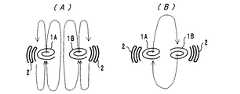
図1(A)に示すように、コイル状の磁界形成パターン1からは、電流が流れることによって、放射状に磁界が発生する。この磁界はパターン面の側方に広がってしまう。そこで、本発明に係る高周波結合器は、図1(B)に示すように、磁界形成パターン1の周囲につづら折りされた周回パターン2を配置した。この周回パターン2に電流が流れることにより、磁界形成パターン1から放射された磁界のうちパターン面の側方に広がる磁界が周回パターン2によって遮蔽される。これにより、磁界がパターン面とほぼ直交する一定の方向に伸びることになり、指向性を固定し、他の通信装置との干渉がなく、近距離で効率よく高周波信号を伝達することができ、特に、広帯域周波数を使った通信方式などの近距離での大容量のデータ通信に好適に用いることができる。(Refer to the schematic configuration of the high-frequency coupler, FIGS. 1 and 2)
As shown in FIG. 1A, a magnetic field is generated radially from the coiled magnetic
磁界形成パターン1から磁界が放射されるが、磁界形成パターン1自体は通信周波数で共振しないので、広い周波数帯域で磁界が放射される。通信距離は磁界形成パターン1の巻数や面積を増加させることで長くすることができる。 A magnetic field is radiated from the magnetic
図1(B)に示すように、周回パターン2は磁界形成パターン1に近接して配置され、互いに隣り合う磁界形成パターン1及び周回パターン2は、逆向きに周回していることが好ましい。隣接する磁界形成パターン1及び周回パターン2で電流が逆向きに流れることで、方向の異なる磁界が形成され磁界の遮断効果が向上する。また、周回パターン2は複数周にわたって周回しており、互いに隣り合う周回パターン2は互いに逆向きに周回していることが好ましい。互いに隣り合う周回パターン2で電流が逆向きに流れ、互いに隣り合う周回パターン2が方向の異なる磁界を形成し、これらが互いに相殺する。これにより、周回パターン2の磁界が形成される領域は全体として磁界を形成しない。この結果、磁界形成パターン1から放射される磁界は、全体として磁界を形成しない複数周の周回パターン2により遮断される。即ち、磁界形成パターン1から放射される磁界を複数周の周回パターン2によって確実に遮蔽することができる。 As shown in FIG. 1B, it is preferable that the
なお、磁界形成パターン1と周回パターン2の距離が短いと、周回パターン2の周回数を多くする必要があるが、側方への磁界の遮断効果は大きい。反対に、磁界形成パターン1と周回パターン2の距離が長いと、周回パターン2の周回数は少なくてよいが、パターン面に垂直な方向だけでなく、斜め方向にも磁界が広がる。よって、磁界形成パターン1と周回パターン2との距離により、磁界の放射角度を制御することができる。 When the distance between the magnetic
周回パターン2を磁界形成パターン1に近接配置すると、両者は磁界形成パターン1のインダクタンス値を小さくするように磁気結合する。このため、一定のインダクタンス値を得るためには、磁界形成パターン1のインダクタンス値を大きくする必要がある。例えば、磁界形成パターン1の巻数や面積を大きくすることで、磁界の放射をパターン面と直交する方向に大きく伸ばして通信距離を長くすることができる。 When the
図1(C)に示すように、磁界形成パターン1による磁界形成方向の一方に磁性体シート3が設けられていてもよい。磁性体シート3は例えばフェライトからなる。磁界形成パターン1からはパターン面に垂直な両方向に磁界が放射される。磁性体シート3によって一方の磁界が吸収されるので、磁界は他の方向にのみ放射され、高周波信号の伝達効率が向上する。また、磁性体シート3側に金属材などが配置されていても高周波結合器がそれからの影響を受けることが非常に少ない。このような磁性体シート3は磁界形成パターン1と平面視で重なっており、さらに周回パターン2とも平面視で重なっていることが好ましい。 As shown in FIG. 1C, a
図2に示すように、磁界形成パターンは二つの周回したパターン1A,1Bで構成されていてもよい。この場合、二つのパターン1A,1Bは同方向に周回していてもよく(図2(A)参照、磁場が同相となる)、あるいは、逆方向に周回していてもよい(図2(B)参照、磁場が逆相となる)。いずれであっても、同じ方向に磁界が形成され、一定の方向に効率よく磁界を形成できる。 As shown in FIG. 2, the magnetic field forming pattern may be composed of two
(通信装置の概略構成、図3参照)
本発明に係る通信装置は、図3に示すように、前記磁界形成パターン1と周回パターン2を設けた高周波結合器10を通信回路部(送信回路11、受信回路12)と接続したもので、受信回路12に接続されている高周波結合器10を送信回路11に接続されている高周波結合器10に30mm程度に近接させることで、1GHz以上の高周波の広帯域信号を用いる通信方式で大容量データを短時間で送受することができる。(Schematic configuration of communication device, see FIG. 3)
As shown in FIG. 3, the communication device according to the present invention comprises a high-
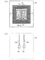
(第1実施例、図4参照)
第1実施例である高周波結合器は、図4に示すように、樹脂製のシート20の表面に磁界形成パターン1A,1Bを近接して配置し、該磁界形成パターン1A,1Bの周囲に周回パターン2を配置し、さらに、シート20の裏面に電極15A,15Bを配置したものである。パターン1A,1B,2及び電極15A,15Bは、アルミ箔、銅箔などの導電材からなる金属薄板をシート20上に貼着してパターニングしたり、あるいは、シート20上にAl、Cu、Agなどの導電性ペーストを塗布したり、めっき処理により設けた膜をパターニングすることにより形成される。(Refer to FIG. 4 in the first embodiment)
As shown in FIG. 4, the high frequency coupler according to the first embodiment has magnetic
磁界形成パターン1A,1Bは一端に電極部25a,25bが形成され、他端が線路26に接続(接続点26a)されている。周回パターン2は折返し部2a,2bによって複数周にわたって逆向きに周回している。線路26の他端は周回パターン2の長さ方向の中央部分2cで電気的に接続されている。電極部25a,25bはシート20の裏面に設けた電極15A,15Bの電極部16a,16bと対向しており、それらの間でコンデンサが形成される。磁界形成パターン1A,1Bは、それぞれ、電極部25a,16a、電極部25b,16bを介して容量結合している。そして、電極15A,15Bのいずれかの端部が通信回路部(送信回路11又は受信回路12)と電気的に接続される。 In the magnetic
なお、通信回路部(送信回路11又は受信回路12)と電気的に接続されない端部は、開放端となる。例えば、電極15Bの端部を接続せず開放端とすると、電極15Bの端部は磁界形成パターン1Bの先端部となる。そして、この電極15Bの端部は、電極部16bと電極部25bにより静電容量を形成し、周回パターン2の中央部分2cに接続されている。ここで、周回パターン2の中央部分2cは電圧が最少の部分であり、回路的には仮想グランドとなっているので、電極15Bはグランドに向かって静電容量を形成していることになる。 Note that an end portion that is not electrically connected to the communication circuit unit (the
電極部16a,16bと電極部25a,25bとの間に形成されるコンデンサは、通信回路部と磁界形成パターン1A,1Bとのインピーダンスマッチングを取るためのものである。 The capacitors formed between the
本第1実施例における基本的な作用効果、即ち、磁界形成パターン1A,1Bから放射される磁界のうちパターン面の側方に広がる磁界が周回パターン2によって遮蔽され、磁界がパターン面と直交する一定の方向に伸び、30mm程度の近距離で効率よく高周波信号を伝達できる点などは図1及び図2を参照して前述したとおりである。特に、第1実施例では、磁界形成パターン1A,1Bが同じ方向に周回している。これにて、同じ方向の磁界が合成され、通信距離が向上する。 The basic operational effects of the first embodiment, that is, the magnetic field radiating from the magnetic
また、本第1実施例では、周回パターン2は折返したダイポール型アンテナとして形成されている。ダイポール型アンテナは広い通過帯域を得ることができる。周回パターン2がダイポール型である場合、周回パターン2の長さはλ/2(λ:所定周波数)の整数倍であることが好ましい。周回パターン2が共振するので、エネルギーの伝達効率が向上する。また、磁界形成パターン1A,1Bと周回パターン2とは、周回パターン2の長さ方向の中央部分2cで電気的に接続されているため、信号の伝達効率が最大となる。即ち、周回パターン2の通過帯域で磁界形成パターン1A,1Bに電流が流れ、磁界が形成される。周回パターン2の長さ方向の中央部分2cは電流が最大で電圧が最小となり、電流最大点は電流により発生する磁界の強さが最大になるので、信号の伝達効率も最大になる。 In the first embodiment, the
周回パターン2は電界アンテナとしても機能する。その共振周波数を広帯域周波数を使った通信方式の使用周波数に合わせると、広帯域な共振器になる。そして、磁界形成パターン1A,1Bと周回パターン2とが中央部分2cで結合することで、磁界形成パターン1A,1Bが周回パターン2(電界アンテナ)の通過周波数帯で磁界を発生する。周回パターン2がダイポール型であると、500MHz以上の帯域幅を得ることができ、本第1実施例のように折返しダイポール型であっても同等の帯域幅を得ることができる。 The
また、本第1実施例である高周波結合器は、シート20の表裏面にパターン1A,1B,2と電極15A,15Bを形成するだけであり、厚さは約0.15〜0.6mmと薄く、面積も周回パターン2の外形サイズで5〜7mm四方であり、非常に小型である。 Further, the high frequency coupler according to the first embodiment only forms the
(第2実施例、図5参照)
第2実施例である高周波結合器は、図5に示すように、基本的には前記第1実施例と同様の構成からなる。第2実施例において特徴的な構成は、周回パターン2の折返し部2bが平面視で異なる周回位置に配置されている。磁界形成パターン1A,1Bから放射された磁界の側方の通過経路が小さくなり、磁界を確実に遮蔽することができる。その他の作用効果は第1実施例と同様である。(Refer to the second embodiment, FIG. 5)
As shown in FIG. 5, the high-frequency coupler according to the second embodiment basically has the same configuration as that of the first embodiment. A characteristic configuration in the second embodiment is that the folded-
(第3実施例、図6参照)
第3実施例である高周波結合器は、図6に示すように、基本的には前記第1実施例と同様の構成からなる。第3実施例において特徴的な構成は、磁界形成パターン1A,1Bと線路26との接続点26aを磁界形成パターン1A,1Bの間に引き入れたことである。接続点26aの位置によって磁界形成パターン1A,1Bの磁界結合度が変化し、高周波での反射特性をコントロールできる。本第3実施例のように接続点26aを磁界形成パターン1A,1Bの間に深く位置させると、通過帯域が狭くなる。その他の作用効果は第1実施例と同様である。(Refer to the third embodiment, FIG. 6)
As shown in FIG. 6, the high-frequency coupler according to the third embodiment basically has the same configuration as that of the first embodiment. A characteristic configuration in the third embodiment is that a
(第4実施例、図7参照)
第4実施例である高周波結合器は、図7に示すように、基本的には前記第1実施例と同様の構成からなる。第4実施例において特徴的な構成は、周回パターン2の周回数を少なくしたことである。作用効果は第1実施例と同様である。但し、周回パターン2はその線路長が第1実施例と比べて短く、λ/2ではなくなり、ダイポール型ではない。(Refer to the fourth embodiment, FIG. 7)
The high-frequency coupler according to the fourth embodiment basically has the same configuration as that of the first embodiment as shown in FIG. A characteristic configuration in the fourth embodiment is that the number of turns of the
(第5実施例、図8参照)
第5実施例である高周波結合器は、図8に示すように、樹脂製シート20Aの表面に周回パターン2を形成し、その下に位置する樹脂製シート20Bの表面に磁界形成パターン1A,1Bを形成し、シート20Bの裏面に電極15A,15Bを形成し、多層構造としたものである。(Refer to the fifth embodiment, FIG. 8)
As shown in FIG. 8, the high-frequency coupler according to the fifth embodiment forms a
磁界形成パターン1A,1Bに接続されている線路26の端部26bと周回パターン2の中央部分2cとはビアホール導体30によって接続されている。また、周回パターン2は両端部が開放されたダイポール型である。本第5実施例の作用効果は基本的には前記各実施例と同様である。特に、第5実施例では磁界形成パターン1A,1Bが互いに逆方向に周回している。異なる方向の磁界がそれぞれ相殺し、一つの磁気ループを形成する。これにより、パターン面の側方に放射する磁界が少なくなるので、周回パターン2の周回数を少なくすることができる。 The
(第6実施例、図9参照)
第6実施例である高周波結合器は、図9に示すように、前記第5実施例と同様に積層構造としたもので、第1層目に周回パターン2を形成し、第2層目に磁界形成パターン1A,1Bを形成し、第3層目に電極15A,15Bを形成している。なお、図9では樹脂製シートの図示を省略している。(See the sixth embodiment, FIG. 9)
As shown in FIG. 9, the high-frequency coupler according to the sixth embodiment has a laminated structure similar to the fifth embodiment, and the
周回パターン2は、線路26とビアホール導体30で接続されており、両端部が開放されたダイポール型である。本第6実施例の作用効果は基本的には前記各実施例と同様である。 The
(第7実施例、図10参照)
第7実施例である高周波結合器は、図10に示すように、樹脂製シート20の表面のほぼ中央部に磁界形成パターン1を配置し、その周囲を囲むように周回パターン2を配置したもので、磁界形成パターン1の一端に設けた電極部25がシート20の裏面に配置した電極15の電極部16と対向し、コンデンサを形成している。そして、電極15の他端に設けた電極部17が通信回路部と電気的に接続される。(Refer to the seventh embodiment, FIG. 10)
As shown in FIG. 10, the high-frequency coupler according to the seventh embodiment has a magnetic
本第7実施例において、周回パターン2は、言わば、グランド電極であり、磁界形成パターン1から放射されてパターン面の側方に広がる磁界を遮蔽し、磁界をパターン面と直交する一定方向に伸ばす。従って、その作用効果は基本的に前記第1実施例と同様である。 In the seventh embodiment, the
(第8実施例、図11参照)
第8実施例である高周波結合器は、図11に示すように、前記第7実施例に示した磁界形成パターン1を周回パターン2の中央部分2cに接続したものである。磁界形成パターン1を周回パターン2に接続する場合は、電流損が生じないように、周回パターン2に切欠き2dを形成する必要がある。本第8実施例の作用効果は第7実施例と同様である。(See the eighth embodiment, FIG. 11)
As shown in FIG. 11, the high-frequency coupler according to the eighth embodiment is obtained by connecting the magnetic
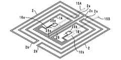
(第9実施例、図12及び図13参照)
第9実施例である高周波結合器は、図12に示すように、樹脂製のシート40の表面に磁界アンテナパターン50を形成し、該パターン50の内側(好ましくは中心部分)に磁界形成パターンと周回パターンとからなる高周波結合器10(例えば、前記第2実施例に示した高周波結合器)を配置したものである。磁界アンテナパターン50はループ状に周回しており、一端50aがビアホール導体55を介してシート40の裏面に形成した線路電極56の一端と接続され、該線路電極56の他端はビアホール導体57を介してシート40の表面に形成した電極51と接続されている。互いに隣接する磁界アンテナパターン50の他端50bと電極51とが非接触型ICカード方式の通信回路部(図示せず)に接続されている。これにて、磁界アンテナパターン50が非接触型ICカード方式による通信アンテナとして機能する。磁界アンテナパターン50の共振周波数は磁界形成パターンの通信周波数よりも低く、非接触型ICカード方式の通信周波数である13.56MHzに対応している。(Refer to the ninth embodiment, FIG. 12 and FIG. 13)
As shown in FIG. 12, the high-frequency coupler according to the ninth embodiment forms a magnetic
なお、互いに隣接する磁界アンテナパターン50の他端50bと電極51とに従来周知の無線ICを搭載してもよい。 A conventionally known wireless IC may be mounted on the
本第9実施例では、磁界形成パターンを用いた広帯域周波数を使った通信と磁界アンテナパターン50を用いた非接触型ICカード方式による通信とを併用して実行することができる。例えば、コンビニエンスストアなどで画像や音楽などの大容量データの受信と課金処理を同時に行うことができる。 In the ninth embodiment, communication using a broadband frequency using a magnetic field forming pattern and communication using a non-contact type IC card method using a magnetic
磁界アンテナパターン50は比較的大きなループで形成されるため、その内側に磁界形成パターン及び周回パターンを配置すればコンパクトにまとめることができる。なお、従来の電界結合方式の結合器にあっては、グランド電極が必要であることから、磁界アンテナパターン50と組み合わせることは不可能であった。 Since the magnetic
ところで、磁界アンテナパターン50の中心部分に磁界形成パターンが配置されていることが好ましい。磁界形成パターンは極めて小サイズであり、相手方アンテナとの位置合わせが困難である。一方、比較的大きなループの磁界アンテナパターン50は通信時に相手方アンテナとの位置合わせが容易であり、それに合わせて磁界形成パターンが相手方パターンと正確に位置合わせされることになる。例えば、磁界アンテナパターン50の中心部分を外部から認識できるように、マーク等をつければ、そのマーク等を用いて位置合わせすることにより、磁界形成パターンの位置合わせも正確にすることができる。 By the way, it is preferable that the magnetic field forming pattern is disposed in the central portion of the magnetic
図13に、携帯電話機などの通信装置に内蔵されたプリント配線回路基板60に搭載された通信回路部との接続形態を示す。高周波結合器10の電極部16a(図4参照)は接続用ピン61とランド62とを介して広帯域周波数を使った通信方式の通信回路部と電気的に接続されている。また、磁界アンテナパターン50は接続用ピン63とランド64とを介して非接触型ICカード方式の通信回路部と電気的に接続されている。高周波結合器10の接続用ピン61は、高価な高周波用のものを使用する必要はなく、安価な低周波用のピン63と同じものを使用することができる。 FIG. 13 shows a connection form with a communication circuit unit mounted on a printed
なお、図13に示す符号3は厚さ500μm程度の磁性体シートであって、磁性体シート3は、磁界形成パターンと周回パターンとからなる高周波結合器10から磁界アンテナパターン50にまで平面視で重なっている。その作用効果は図1(C)を参照して説明したとおり、パターン面に垂直な両方向に放射される磁界のうち一方の磁界を吸収し、他の方向にのみ放射させるためであり、また、携帯電話機に内蔵されている電池などの金属部分の影響を排除することができる。 Note that
(第10実施例、図14参照)
第10実施例である高周波結合器は、図14に示すように、シート20の表面に、磁界形成パターン1A,1Bを近接して配置し、該磁界形成パターン1A,1Bの周囲に周回パターン2を配置し、さらに、シート20の裏面に電極15A,15Bを配置したもので、基本的には前記第3実施例(図6参照)と同様の構成を備えている。本第10実施例では、さらに、周回パターン2の長さ方向の中央部分2cに接続部2dを形成し、該接続部2dに金属板70を柱状部71を介して電気的に接続している。金属板70はその4隅に設けた支柱72にてシート20上に磁界形成パターン1A,1Bや周回パターン2を覆うように配置されている。(10th embodiment, see FIG. 14)
As shown in FIG. 14, the high-frequency coupler according to the tenth embodiment has magnetic
本第10実施例においては、周回パターン2の中央部分2cに金属板70を電気的に接続しているため、広い帯域で電界を送受信することができ、エネルギー伝達効率が向上する。 In the tenth embodiment, since the
(他の実施例)
なお、本発明に係る高周波結合器及び通信装置は前記実施例に限定するものではなく、その要旨の範囲内で種々に変更できることは勿論である。(Other examples)
The high-frequency coupler and the communication device according to the present invention are not limited to the above-described embodiments, and can be variously modified within the scope of the gist.
以上のように、本発明は、高周波結合器及び通信装置に有用であり、特に、小型で、効率よく近距離での大容量のデータ通信が可能である点で優れている。 As described above, the present invention is useful for a high-frequency coupler and a communication device, and is particularly excellent in that it is small in size and can efficiently perform large-capacity data communication at a short distance.
1,1A,1B…磁界形成パターン
2…周回パターン
2a,2b…折返し部
2c…中央部分
3…磁性体シート
10…高周波結合器
11…送信回路
12…受信回路
50…磁界アンテナパターン
60…プリント配線回路基板
61…接続用ピン
62…ランド
70…金属板DESCRIPTION OF
Claims (21)
Translated fromJapanese折返し部を含み、前記磁界形成パターンの近傍に配置され、磁界形成パターンから発生してパターン面の側方に広がる磁界を遮蔽する折返しパターンと、
を備えたことを特徴とする高周波結合器。A magnetic field forming pattern for forming a magnetic field in a certain direction;
It includes a folded portion, wherein disposed in thevicinity of the magnetic field forming pattern, afolding pattern for shielding the magnetic field extending to the side of the pattern surface was produced from the magnetic-field forming pattern,
A high-frequency coupler comprising:
前記折返しパターン及び前記磁界形成パターンは、前記折返しパターンと前記磁界形成パターンのうち隣り合うパターンに互いに逆向きに電流が流れるように接続されていること、
を特徴とする請求項1に記載の高周波結合器。Thefolded patternis disposedso as to surround said magnetic field forming pattern,
The folded pattern and the magnetic field forming pattern are connected so that currents flow in opposite directions to adjacent patterns of the folded pattern and the magnetic field forming pattern ;
The high-frequency coupler according to claim 1.
前記磁界形成パターン及び前記折返しパターンは前記磁界アンテナパターンの内側に配置されていること、
を特徴とする請求項1ないし請求項14のいずれかに記載の高周波結合器。A magnetic antenna pattern;
The magnetic field forming pattern and thefolded pattern are disposed inside the magnetic field antenna pattern;
The high-frequency coupler according to claim 1, wherein
データを伝送する高周波信号の処理を行う通信回路部と、
を備えたことを特徴とする通信装置。A magnetic field forming patterns for forming a magnetic field in a predetermined direction, comprises a folded portion,wherein disposed in thevicinity of the magnetic field forming pattern, afolding pattern for shielding the magnetic field extending to the side of the pattern surface was produced from the magnetic-field forming pattern, A high frequency coupler comprising:
A communication circuit unit for processing a high-frequency signal for transmitting data;
A communication apparatus comprising:
Priority Applications (1)
| Application Number | Priority Date | Filing Date | Title |
|---|---|---|---|
| JP2010526090AJP5257452B2 (en) | 2008-12-15 | 2009-12-03 | High frequency coupler and communication device |
Applications Claiming Priority (4)
| Application Number | Priority Date | Filing Date | Title |
|---|---|---|---|
| JP2008318996 | 2008-12-15 | ||
| JP2008318996 | 2008-12-15 | ||
| JP2010526090AJP5257452B2 (en) | 2008-12-15 | 2009-12-03 | High frequency coupler and communication device |
| PCT/JP2009/070301WO2010071027A1 (en) | 2008-12-15 | 2009-12-03 | High-frequency coupler and communication device |
Publications (2)
| Publication Number | Publication Date |
|---|---|
| JPWO2010071027A1 JPWO2010071027A1 (en) | 2012-05-24 |
| JP5257452B2true JP5257452B2 (en) | 2013-08-07 |
Family
ID=42268699
Family Applications (1)
| Application Number | Title | Priority Date | Filing Date |
|---|---|---|---|
| JP2010526090AExpired - Fee RelatedJP5257452B2 (en) | 2008-12-15 | 2009-12-03 | High frequency coupler and communication device |
Country Status (6)
| Country | Link |
|---|---|
| US (2) | US8193873B2 (en) |
| JP (1) | JP5257452B2 (en) |
| KR (1) | KR101230416B1 (en) |
| CN (1) | CN102246348B (en) |
| DE (1) | DE112009003563B4 (en) |
| WO (1) | WO2010071027A1 (en) |
Families Citing this family (29)
| Publication number | Priority date | Publication date | Assignee | Title |
|---|---|---|---|---|
| JP4843611B2 (en) | 2004-10-01 | 2011-12-21 | デ,ロシェモント,エル.,ピエール | Ceramic antenna module and manufacturing method thereof |
| KR100978271B1 (en)* | 2008-04-01 | 2010-08-26 | 엘에스산전 주식회사 | RFID tag using built-in antenna and RFID system using same |
| US7959598B2 (en) | 2008-08-20 | 2011-06-14 | Asante Solutions, Inc. | Infusion pump systems and methods |
| JP5257452B2 (en)* | 2008-12-15 | 2013-08-07 | 株式会社村田製作所 | High frequency coupler and communication device |
| US8952858B2 (en)* | 2009-06-17 | 2015-02-10 | L. Pierre de Rochemont | Frequency-selective dipole antennas |
| US8922347B1 (en) | 2009-06-17 | 2014-12-30 | L. Pierre de Rochemont | R.F. energy collection circuit for wireless devices |
| WO2012036221A1 (en)* | 2010-09-15 | 2012-03-22 | ソニーケミカル&インフォメーションデバイス株式会社 | Antenna device and communication device |
| JP5727177B2 (en)* | 2010-09-15 | 2015-06-03 | デクセリアルズ株式会社 | ANTENNA DEVICE AND COMMUNICATION DEVICE |
| JP5790200B2 (en)* | 2011-06-27 | 2015-10-07 | ソニー株式会社 | Communication apparatus and communication system |
| KR101448024B1 (en)* | 2012-05-15 | 2014-10-07 | 스미다 코포레이션 가부시키가이샤 | Contactless power transmission system and transmission coil for contactless power transmission |
| US9561324B2 (en) | 2013-07-19 | 2017-02-07 | Bigfoot Biomedical, Inc. | Infusion pump system and method |
| EP3374905A1 (en) | 2016-01-13 | 2018-09-19 | Bigfoot Biomedical, Inc. | User interface for diabetes management system |
| US10806859B2 (en) | 2016-01-14 | 2020-10-20 | Bigfoot Biomedical, Inc. | Adjusting insulin delivery rates |
| HK1256995A1 (en) | 2016-01-14 | 2019-10-11 | Bigfoot Biomedical, Inc. | Occlusion resolution in medication delivery devices, systems, and methods |
| USD822010S1 (en)* | 2016-02-26 | 2018-07-03 | Byte Foods, Inc. | RFID tag antenna |
| US12383166B2 (en) | 2016-05-23 | 2025-08-12 | Insulet Corporation | Insulin delivery system and methods with risk-based set points |
| US10363374B2 (en) | 2016-05-26 | 2019-07-30 | Insulet Corporation | Multi-dose drug delivery device |
| EP3500161A4 (en) | 2016-12-12 | 2020-01-08 | Bigfoot Biomedical, Inc. | ALARMS AND WARNINGS FOR MEDICINE DELIVERY DEVICES AND RELATED SYSTEMS AND METHODS |
| US10758675B2 (en) | 2017-01-13 | 2020-09-01 | Bigfoot Biomedical, Inc. | System and method for adjusting insulin delivery |
| EP3568859A1 (en) | 2017-01-13 | 2019-11-20 | Bigfoot Biomedical, Inc. | Insulin delivery methods, systems and devices |
| US10500334B2 (en) | 2017-01-13 | 2019-12-10 | Bigfoot Biomedical, Inc. | System and method for adjusting insulin delivery |
| US10881792B2 (en) | 2017-01-13 | 2021-01-05 | Bigfoot Biomedical, Inc. | System and method for adjusting insulin delivery |
| USD874471S1 (en) | 2017-06-08 | 2020-02-04 | Insulet Corporation | Display screen with a graphical user interface |
| USD928199S1 (en) | 2018-04-02 | 2021-08-17 | Bigfoot Biomedical, Inc. | Medication delivery device with icons |
| USD920343S1 (en) | 2019-01-09 | 2021-05-25 | Bigfoot Biomedical, Inc. | Display screen or portion thereof with graphical user interface associated with insulin delivery |
| US11228111B2 (en)* | 2019-04-11 | 2022-01-18 | International Business Machines Corporation | Compact dipole antenna design |
| EP3787105B1 (en) | 2019-08-30 | 2025-07-09 | Rohde & Schwarz GmbH & Co. KG | Wideband coupler |
| USD977502S1 (en) | 2020-06-09 | 2023-02-07 | Insulet Corporation | Display screen with graphical user interface |
| US12097355B2 (en) | 2023-01-06 | 2024-09-24 | Insulet Corporation | Automatically or manually initiated meal bolus delivery with subsequent automatic safety constraint relaxation |
Citations (3)
| Publication number | Priority date | Publication date | Assignee | Title |
|---|---|---|---|---|
| JP2005051536A (en)* | 2003-07-29 | 2005-02-24 | Hitachi Kokusai Electric Inc | Dual frequency antenna device |
| JP2007523562A (en)* | 2004-02-20 | 2007-08-16 | スリーエム イノベイティブ プロパティズ カンパニー | Multiple loop antenna for radio frequency identification (RFID) communication |
| JP2008160874A (en)* | 2006-04-14 | 2008-07-10 | Murata Mfg Co Ltd | Wireless ic device |
Family Cites Families (22)
| Publication number | Priority date | Publication date | Assignee | Title |
|---|---|---|---|---|
| US5914692A (en)* | 1997-01-14 | 1999-06-22 | Checkpoint Systems, Inc. | Multiple loop antenna with crossover element having a pair of spaced, parallel conductors for electrically connecting the multiple loops |
| FR2840430B1 (en)* | 2002-05-29 | 2005-01-14 | Gemplus Card Int | DECORATIVE CONTACTLESS COMMUNICATION ASSEMBLY FOR INTELLIGENT PORTABLE OBJECT WITH TRANSPARENT BODY |
| JP3982476B2 (en)* | 2003-10-01 | 2007-09-26 | ソニー株式会社 | Communications system |
| DE602005002799T2 (en)* | 2004-08-21 | 2008-02-07 | Samsung Electronics Co., Ltd., Suwon | Small rectifying antenna |
| DE602005021513D1 (en)* | 2004-08-26 | 2010-07-08 | Nxp Bv | RFID LABEL WITH FOLDED DIPOL |
| US7545328B2 (en)* | 2004-12-08 | 2009-06-09 | Electronics And Telecommunications Research Institute | Antenna using inductively coupled feeding method, RFID tag using the same and antenna impedance matching method thereof |
| JP2006180043A (en)* | 2004-12-21 | 2006-07-06 | Hitachi Maxell Ltd | Electronic tag system |
| US7714794B2 (en)* | 2005-01-19 | 2010-05-11 | Behzad Tavassoli Hozouri | RFID antenna |
| JP4626447B2 (en)* | 2005-08-26 | 2011-02-09 | パナソニック電工株式会社 | Non-contact IC card reader device |
| DE102005042444B4 (en)* | 2005-09-06 | 2007-10-11 | Ksw Microtec Ag | Arrangement for an RFID transponder antenna |
| JP2007073015A (en)* | 2005-09-09 | 2007-03-22 | Omron Corp | Non-contact ic tag inlet, non-contact ic tag, and antenna |
| US7374105B2 (en)* | 2005-10-29 | 2008-05-20 | Magnex Corporation | RFID tag with improved range |
| JP4345851B2 (en) | 2006-09-11 | 2009-10-14 | ソニー株式会社 | Communication system and communication apparatus |
| JP4798223B2 (en)* | 2006-10-27 | 2011-10-19 | 株式会社村田製作所 | Article with electromagnetic coupling module |
| DE102006055744A1 (en)* | 2006-11-25 | 2008-05-29 | Atmel Germany Gmbh | Antenna for rear scatter-based passive or semi passive transponder of radio frequency identification system, has branch with section connected with another section, where thin layer of branch and integrated circuit are formed on substrate |
| US8237622B2 (en)* | 2006-12-28 | 2012-08-07 | Philtech Inc. | Base sheet |
| TWI347032B (en)* | 2006-12-29 | 2011-08-11 | Delta Networks Inc | Method for increasing bandwidth of an antenna and wide bandwidth antenna structure |
| ATE555453T1 (en)* | 2007-04-06 | 2012-05-15 | Murata Manufacturing Co | RADIO IC DEVICE |
| JP4544289B2 (en)* | 2007-11-09 | 2010-09-15 | ソニー株式会社 | COMMUNICATION DEVICE, COMMUNICATION METHOD, AND COMMUNICATION SYSTEM |
| JP5257452B2 (en)* | 2008-12-15 | 2013-08-07 | 株式会社村田製作所 | High frequency coupler and communication device |
| EP2385580B1 (en)* | 2009-01-30 | 2014-04-09 | Murata Manufacturing Co., Ltd. | Antenna and wireless ic device |
| JP5329271B2 (en)* | 2009-03-19 | 2013-10-30 | タイコエレクトロニクスジャパン合同会社 | High frequency coupler |
- 2009
- 2009-12-03JPJP2010526090Apatent/JP5257452B2/ennot_activeExpired - Fee Related
- 2009-12-03WOPCT/JP2009/070301patent/WO2010071027A1/enactiveApplication Filing
- 2009-12-03DEDE112009003563.9Tpatent/DE112009003563B4/ennot_activeExpired - Fee Related
- 2009-12-03KRKR1020117013061Apatent/KR101230416B1/ennot_activeExpired - Fee Related
- 2009-12-03CNCN2009801515534Apatent/CN102246348B/ennot_activeExpired - Fee Related
- 2011
- 2011-06-14USUS13/159,491patent/US8193873B2/ennot_activeExpired - Fee Related
- 2012
- 2012-05-03USUS13/462,841patent/US8400231B2/ennot_activeExpired - Fee Related
Patent Citations (3)
| Publication number | Priority date | Publication date | Assignee | Title |
|---|---|---|---|---|
| JP2005051536A (en)* | 2003-07-29 | 2005-02-24 | Hitachi Kokusai Electric Inc | Dual frequency antenna device |
| JP2007523562A (en)* | 2004-02-20 | 2007-08-16 | スリーエム イノベイティブ プロパティズ カンパニー | Multiple loop antenna for radio frequency identification (RFID) communication |
| JP2008160874A (en)* | 2006-04-14 | 2008-07-10 | Murata Mfg Co Ltd | Wireless ic device |
Also Published As
| Publication number | Publication date |
|---|---|
| DE112009003563T5 (en) | 2012-09-20 |
| KR101230416B1 (en) | 2013-02-06 |
| CN102246348B (en) | 2013-12-18 |
| US8193873B2 (en) | 2012-06-05 |
| WO2010071027A1 (en) | 2010-06-24 |
| KR20110086590A (en) | 2011-07-28 |
| CN102246348A (en) | 2011-11-16 |
| DE112009003563B4 (en) | 2014-05-08 |
| US20110241804A1 (en) | 2011-10-06 |
| US8400231B2 (en) | 2013-03-19 |
| US20120218071A1 (en) | 2012-08-30 |
| JPWO2010071027A1 (en) | 2012-05-24 |
Similar Documents
| Publication | Publication Date | Title |
|---|---|---|
| JP5257452B2 (en) | High frequency coupler and communication device | |
| JP6614363B2 (en) | ANTENNA DEVICE AND ELECTRONIC DEVICE | |
| JP5177312B2 (en) | ANTENNA DEVICE AND ELECTRONIC DEVICE | |
| US9768511B2 (en) | Antenna device and wireless communication device | |
| US8240562B2 (en) | Communication apparatus, communication method, antenna module and communication system | |
| JP5578291B2 (en) | Antenna device and communication terminal device | |
| JP2008311960A (en) | Communication system and communication device | |
| JP5672874B2 (en) | Wireless IC tag and RFID system | |
| JP2008312074A (en) | Communication device | |
| TWI539668B (en) | Antenna device and communication device | |
| WO2017104245A1 (en) | Antenna device and electronic apparatus |
Legal Events
| Date | Code | Title | Description |
|---|---|---|---|
| A131 | Notification of reasons for refusal | Free format text:JAPANESE INTERMEDIATE CODE: A131 Effective date:20121218 | |
| A521 | Request for written amendment filed | Free format text:JAPANESE INTERMEDIATE CODE: A523 Effective date:20130214 | |
| RD02 | Notification of acceptance of power of attorney | Free format text:JAPANESE INTERMEDIATE CODE: A7422 Effective date:20130214 | |
| TRDD | Decision of grant or rejection written | ||
| A01 | Written decision to grant a patent or to grant a registration (utility model) | Free format text:JAPANESE INTERMEDIATE CODE: A01 Effective date:20130326 | |
| A61 | First payment of annual fees (during grant procedure) | Free format text:JAPANESE INTERMEDIATE CODE: A61 Effective date:20130408 | |
| FPAY | Renewal fee payment (event date is renewal date of database) | Free format text:PAYMENT UNTIL: 20160502 Year of fee payment:3 | |
| R150 | Certificate of patent or registration of utility model | Free format text:JAPANESE INTERMEDIATE CODE: R150 Ref document number:5257452 Country of ref document:JP Free format text:JAPANESE INTERMEDIATE CODE: R150 | |
| LAPS | Cancellation because of no payment of annual fees |