JP5253875B2 - Nonvolatile semiconductor memory device and manufacturing method thereof - Google Patents
Nonvolatile semiconductor memory device and manufacturing method thereofDownload PDFInfo
- Publication number
- JP5253875B2 JP5253875B2JP2008117508AJP2008117508AJP5253875B2JP 5253875 B2JP5253875 B2JP 5253875B2JP 2008117508 AJP2008117508 AJP 2008117508AJP 2008117508 AJP2008117508 AJP 2008117508AJP 5253875 B2JP5253875 B2JP 5253875B2
- Authority
- JP
- Japan
- Prior art keywords
- layer
- insulating layer
- dummy
- memory
- memory device
- Prior art date
- Legal status (The legal status is an assumption and is not a legal conclusion. Google has not performed a legal analysis and makes no representation as to the accuracy of the status listed.)
- Active
Links
Images


Classifications
- H—ELECTRICITY
- H10—SEMICONDUCTOR DEVICES; ELECTRIC SOLID-STATE DEVICES NOT OTHERWISE PROVIDED FOR
- H10B—ELECTRONIC MEMORY DEVICES
- H10B43/00—EEPROM devices comprising charge-trapping gate insulators
- H10B43/20—EEPROM devices comprising charge-trapping gate insulators characterised by three-dimensional arrangements, e.g. with cells on different height levels
- H10B43/23—EEPROM devices comprising charge-trapping gate insulators characterised by three-dimensional arrangements, e.g. with cells on different height levels with source and drain on different levels, e.g. with sloping channels
- H10B43/27—EEPROM devices comprising charge-trapping gate insulators characterised by three-dimensional arrangements, e.g. with cells on different height levels with source and drain on different levels, e.g. with sloping channels the channels comprising vertical portions, e.g. U-shaped channels
- H—ELECTRICITY
- H10—SEMICONDUCTOR DEVICES; ELECTRIC SOLID-STATE DEVICES NOT OTHERWISE PROVIDED FOR
- H10B—ELECTRONIC MEMORY DEVICES
- H10B43/00—EEPROM devices comprising charge-trapping gate insulators
- H10B43/40—EEPROM devices comprising charge-trapping gate insulators characterised by the peripheral circuit region
- H—ELECTRICITY
- H10—SEMICONDUCTOR DEVICES; ELECTRIC SOLID-STATE DEVICES NOT OTHERWISE PROVIDED FOR
- H10B—ELECTRONIC MEMORY DEVICES
- H10B69/00—Erasable-and-programmable ROM [EPROM] devices not provided for in groups H10B41/00 - H10B63/00, e.g. ultraviolet erasable-and-programmable ROM [UVEPROM] devices
Landscapes
- Semiconductor Memories (AREA)
- Non-Volatile Memory (AREA)
Description
Translated fromJapanese本発明は、電気的にデータの書き換えが可能な不揮発性半導体記憶装置、及びその製造方法に関する。 The present invention relates to a nonvolatile semiconductor memory device capable of electrically rewriting data and a method for manufacturing the same.
従来、シリコン基板上の2次元平面内に素子を集積して、LSIが形成されてきた。メモリの記憶容量を増加させるには、一素子の寸法を小さくする(微細化する)方法があるが、近年その微細化もコスト的、技術的に困難なものになってきた。微細化のためにはフォトリソグラフィの技術向上が必要であるが、例えば、現在のArF液浸露光技術では40nm付近のルールが解像限界となっており、更なる微細化のためにはEUV露光機の導入が必要である。しかし、EUV露光機はコスト高であり、コストを考えた場合には現実的ではない。また、仮に微細化が達成されたとしても、駆動電圧などがスケーリングされない限り、素子間の耐圧など物理的な限界点を迎える事が予想される。つまり、デバイスとしての動作が困難になる可能性が高い。 Conventionally, LSIs have been formed by integrating elements in a two-dimensional plane on a silicon substrate. In order to increase the storage capacity of the memory, there is a method of reducing (miniaturizing) the size of one element, but in recent years, the miniaturization has become difficult in terms of cost and technology. For miniaturization, photolithography technology needs to be improved. For example, in the current ArF immersion exposure technology, the rule near 40 nm is the resolution limit, and for further miniaturization, EUV exposure is required. It is necessary to introduce a machine. However, the EUV exposure apparatus is expensive, and it is not realistic when considering the cost. Even if miniaturization is achieved, it is expected that physical limits such as breakdown voltage between elements will be reached unless the drive voltage is scaled. That is, there is a high possibility that operation as a device is difficult.
そこで、近年、メモリの集積度を高めるために、メモリセルを3次元的に配置した半導体記憶装置が多数提案されている(特許文献1乃至3参照)。 In recent years, therefore, many semiconductor memory devices in which memory cells are arranged three-dimensionally have been proposed in order to increase the degree of memory integration (see Patent Documents 1 to 3).
メモリセルを3次元的に配置した従来の半導体記憶装置の一つに、円柱型構造のトランジスタを用いた半導体記憶装置がある(特許文献1乃至3)。円柱型構造のトランジスタを用いた半導体記憶装置においては、ゲート電極となる多層に積層された積層導電層、及びピラー状の柱状半導体が設けられる。柱状半導体は、トランジスタのチャネル(ボディ)部として機能する。柱状半導体の周りには、電荷を蓄積可能なメモリゲート絶縁層が設けられる。これら積層導電層、柱状半導体、メモリゲート絶縁層を含む構成は、メモリストリングスと呼ばれる。 As one of conventional semiconductor memory devices in which memory cells are arranged three-dimensionally, there is a semiconductor memory device using a transistor having a cylindrical structure (Patent Documents 1 to 3). In a semiconductor memory device using a transistor having a columnar structure, a stacked conductive layer and a pillar-shaped columnar semiconductor that are stacked in multiple layers to be a gate electrode are provided. The columnar semiconductor functions as a channel (body) portion of the transistor. A memory gate insulating layer capable of storing electric charge is provided around the columnar semiconductor. A configuration including these stacked conductive layers, columnar semiconductors, and memory gate insulating layers is called a memory string.
上記メモリストリングスを形成する工程においては、複数回の化学機械研磨(CMP:Chemical Mechanical Polishing)が行なわれる。このCMPにおいては、基板上にメモリ層、及びCMP用ダミー層が設けられる。メモリ層は、CMP処理により平坦化を望む領域である。CMP用ダミー層は、CMPによるメモリ層の平坦化に際して、メモリ層の研磨面を所望の面に平行とするために用いられるストッパーとして機能する層である。 In the process of forming the memory strings, chemical mechanical polishing (CMP) is performed a plurality of times. In this CMP, a memory layer and a CMP dummy layer are provided on a substrate. The memory layer is a region where planarization is desired by CMP processing. The CMP dummy layer is a layer that functions as a stopper used to make the polished surface of the memory layer parallel to a desired surface when the memory layer is planarized by CMP.
上記メモリ層及びCMP用ダミー層共に、その占有面積の縮小が望まれている。つまり、半導体記憶装置全体として、その占有面積の縮小が望まれている。
本発明は、占有面積を縮小した不揮発性半導体記憶装置、及びその製造方法を提供する。 The present invention provides a nonvolatile semiconductor memory device having a reduced occupation area and a method for manufacturing the same.
本発明の一態様に係る不揮発性半導体記憶装置は、電気的に書き換え可能であり且つ直列接続された複数のメモリセルとして機能する第1の層、及び当該第1の層の周辺に設けられた第2の層を備え、前記第1の層は、基板に対して平行に延びると共に前記基板に垂直な方向に積層された複数の第1導電層と、前記複数の第1導電層の上層に形成された第1絶縁層と、当該複数の第1導電層を貫通するように形成された第1半導体層と、前記第1導電層と前記第1半導体層との間に形成され且つ電荷を蓄積可能に構成された電荷蓄積層とを備え、前記第1導電層の端部は、第1方向にて階段状に形成され、前記第2の層は、前記基板に対して平行に延びると共に前記基板に垂直な方向に積層されて前記複数の第1導電層とそれぞれ同層に形成された複数の第2導電層と、前記複数の第2導電層の上層に形成された第2絶縁層とを備え、前記第2導電層の端部は、所定領域にて前記基板に対して略垂直方向に延びる直線に沿って揃うように形成され、前記所定領域は、前記第2の層の上層から下層へと延びる接続導電層及び第3絶縁層により満たされるように構成され、前記接続導電層は、金属にて構成されていることを特徴とする。A nonvolatile semiconductor memory device according to one embodiment of the present invention is provided in the periphery of a first layer that functions as a plurality of memory cells that are electrically rewritable and connected in series. A second layer, the first layer extending parallel to the substrate and stacked in a direction perpendicular to the substrate, and an upper layer of the plurality of first conductive layers A first insulating layer formed; a first semiconductor layer formed to penetrate the plurality of first conductive layers; and a charge formed between the first conductive layer and the first semiconductor layer. And an end portion of the first conductive layer is formed in a staircase shape in the first direction, and the second layer extends in parallel to the substrate. Stacked in a direction perpendicular to the substrate and formed in the same layer as each of the plurality of first conductive layers A plurality of second conductive layers and a second insulating layer formed on the plurality of second conductive layers, and an end portion of the second conductive layer is located in a predetermined region with respect to the substrate. Thepredetermined region is formed so as to be aligned along a straight line extending in a substantially vertical direction,and is configured to be filled with a connection conductive layer and a third insulating layer extending from an upper layer to a lower layer of the second layer, and the connection The conductive layer is made of metal .
本発明の一態様に係る不揮発性半導体記憶装置の製造方法は、電気的に書き換え可能であり且つ直列接続された複数のメモリセルを有する不揮発性半導体記憶装置の製造方法であって、基板に平行に延びる第1導電層を複数層に亘って前記基板上に積層させるように形成する工程と、前記複数層の第1導電層の上層に第1絶縁層を形成する工程と、第1の領域の第1方向の端部にて前記複数の第1導電層を階段状に加工する工程と、前記第1の領域と異なる第2の領域の所定領域にて前記複数の第1導電層を貫通する第1の貫通孔を形成する工程と、当該第1の貫通孔内に第2絶縁層を形成する工程と、前記第1の貫通孔内の前記第2絶縁層を貫通する第2の貫通孔を形成する工程と、前記第2の貫通孔を埋めるように第2導電層を形成する工程とを備え、前記第2導電層は、金属にて構成されていることを特徴とする。
A method for manufacturing a nonvolatile semiconductor memory device according to one embodiment of the present invention is a method for manufacturing a nonvolatile semiconductor memory device having a plurality of memory cells that are electrically rewritable and connected in series, and is parallel to a substrate. A step of forming afirst conductive layer extending in layers so as to be laminated on the substrate, a step of forming afirst insulating layer onthe first conductive layer ofthe plurality of layers, and a first region A step of processing the plurality offirst conductive layers in an end portion in the first direction of the first direction, and penetrating the plurality offirst conductive layers in a predetermined region of a second region different from the first region to forming a first through-hole, the forming asecond insulating layer on the first through hole, a second through-penetratingsaid second insulating layer in said first through hole a step of forming a hole, forming asecond conductive layer to fill the second through holeA degree, the second conductive layer is characterizedby being composed of metal.
本発明は、占有面積を縮小した不揮発性半導体記憶装置、及びその製造方法を提供することが可能となる。 The present invention can provide a nonvolatile semiconductor memory device with a reduced occupation area and a method for manufacturing the same.
以下、図面を参照して、本発明に係る不揮発性半導体記憶装置の実施形態について説明する。 Hereinafter, embodiments of a nonvolatile semiconductor memory device according to the present invention will be described with reference to the drawings.
[第1実施形態]
(第1実施形態に係る不揮発性半導体記憶装置100の構成)
図1は、本発明の第1実施形態に係る不揮発性半導体記憶装置100の概略図を示す。図1に示すように、実施形態に係る不揮発性半導体記憶装置100は、主として、メモリトランジスタ領域(第1の領域)12、ワード線駆動回路13、ソース側選択ゲート線(SGS)駆動回路14、ドレイン側選択ゲート線(SGD)駆動回路15、センスアンプ16を有する。メモリトランジスタ領域12は、データを記憶するメモリトランジスタを有する。ワード線駆動回路13は、ワード線WLにかける電圧を制御する。ソース側選択ゲート線(SGS)駆動回路14は、ソース側選択ゲート線SGSにかける電圧を制御する。ドレイン側選択ゲート線(SGD)駆動回路15は、ドレイン側選択ゲート線SGDにかける電圧を制御する。センスアンプ16は、メモリトランジスタから読み出した電位を増幅する。なお、上記の他、実施形態に係る不揮発性半導体記憶装置100は、ビット線BLにかける電圧を制御するビット線駆動回路、ソース線SLにかける電圧を制御するソース線駆動回路を有する(図示略)。[First Embodiment]
(Configuration of Nonvolatile
FIG. 1 is a schematic view of a nonvolatile
また、図1に示すように、第1実施形態に係る不揮発性半導体記憶装置100において、メモリトランジスタ領域12を構成するメモリトランジスタは、半導体層を複数積層することによって形成されている。また、図1に示すとおり各層のワード線WLは、水平方向において2次元的に広がりを有するように形成されている。各層のワード線WLは、それぞれ同一層からなる板状の平面構造となっている。 As shown in FIG. 1, in the nonvolatile
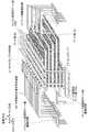
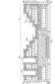
図2は、第1実施形態に係る不揮発性半導体記憶装置100のメモリトランジスタ領域12の一部の概略斜視図である。実施形態においては、メモリトランジスタ領域12は、メモリトランジスタMTr1mn〜MTr4mn、ソース側選択トランジスタSSTrmn及びドレイン側選択トランジスタSDTrmnからなるメモリストリングスMSをm×n個(m、nは自然数)を有している。図2においては、m=3、n=4の一例を示している。 FIG. 2 is a schematic perspective view of a part of the
各メモリストリングスMSのメモリトランジスタMTr1mn〜MTr4mnのゲートに接続されているワード線WL1〜WL4は、それぞれ同一の導電膜によって形成されており、それぞれ共通である。即ち、各メモリストリングスMSのメモリトランジスタMTr1mnのゲートの全てがワード線WL1に接続されている。また、各メモリストリングスMSのメモリトランジスタMTr2mnのゲートの全てがワード線WL2に接続されている。また、各メモリストリングスMSのメモリトランジスタMTr3mnのゲートの全てがワード線WL3に接続されている。また、各メモリストリングスMSのメモリトランジスタMTr4mnのゲートの全てがワード線WL4に接続されている。実施形態に係る不揮発性半導体記憶装置100においては、図1及び図2に示すように、ワード線WL1〜WL4は、それぞれ、半導体基板Baと平行な水平方向において2次元的に広がりを有するように形成されている。また、ワード線WL1〜WL4は、それぞれ、メモリストリングスMSに略垂直に配置されている。また、ワード線WL1〜WL4のロウ方向の端部は、階段状に形成されている。ここで、ロウ方向は、垂直方向に直交する方向であり、カラム方向は、垂直方向及びロウ方向に直交する方向である。 The word lines WL1 to WL4 connected to the gates of the memory transistors MTr1mn to MTr4mn of each memory string MS are formed by the same conductive film and are common to each other. That is, all the gates of the memory transistors MTr1mn of each memory string MS are connected to the word line WL1. Further, all the gates of the memory transistors MTr2mn of each memory string MS are connected to the word line WL2. Further, all the gates of the memory transistors MTr3mn of each memory string MS are connected to the word line WL3. Further, all the gates of the memory transistors MTr4mn of each memory string MS are connected to the word line WL4. In the nonvolatile
各メモリストリングスMSは、半導体基板BaのP−well領域Ba1に形成されたn+領域(後述するBa2)の上に柱状の柱状半導体CLmn(図2に示す場合、m=1〜3、n=1〜4)を有している。各柱状半導体CLmnは、半導体基板Baから垂直方向に形成されており、半導体基板Ba及びワード線WL1〜WL4の面上においてマトリクス状になるように配置されている。つまり、メモリストリングスMSも、柱状半導体CLmnに垂直な面内にマトリクス状に配置されている。なお、この柱状半導体CLmnは、円柱状であっても、角柱状であってもよい。また、柱状半導体CLmnとは、段々形状を有する柱状の半導体を含む。 Each memory string MS has a columnar columnar semiconductor CLmn (in the case of FIG. 2, m = 1 to 3, n = 1) on an n + region (Ba2 described later) formed in the P-well region Ba1 of the semiconductor substrate Ba. To 4). Each columnar semiconductor CLmn is formed in a vertical direction from the semiconductor substrate Ba, and is arranged in a matrix on the surface of the semiconductor substrate Ba and the word lines WL1 to WL4. That is, the memory strings MS are also arranged in a matrix in a plane perpendicular to the columnar semiconductor CLmn. The columnar semiconductor CLmn may be cylindrical or prismatic. The columnar semiconductor CLmn includes a columnar semiconductor having a stepped shape.
また、図2に示すように、メモリストリングスMSの上方には、柱状半導体CLmnと絶縁膜(図示せず)を介し接してドレイン側選択トランジスタSDTrmnを構成する矩形板状のドレイン側選択ゲート線SGD(図2に示す場合、SGD1〜SGD4)が設けられている。各ドレイン側選択ゲート線SGDは、互いに絶縁分離され、ワード線WL1〜WL4とは異なり、ロウ方向に延びカラム方向に繰り返し設けられたライン状に形成されている。また、ドレイン側選択ゲート線SGDのカラム方向の中心を貫通して、柱状半導体CLmnが設けられている。 Further, as shown in FIG. 2, a rectangular plate-shaped drain-side selection gate line SGD that forms a drain-side selection transistor SDTrmn in contact with the columnar semiconductor CLmn via an insulating film (not shown) is disposed above the memory string MS. (In the case shown in FIG. 2, SGD1 to SGD4) are provided. Each drain-side selection gate line SGD is insulated and separated from each other, and is formed in a line extending in the row direction and repeatedly provided in the column direction, unlike the word lines WL1 to WL4. A columnar semiconductor CLmn is provided so as to penetrate the center in the column direction of the drain-side selection gate line SGD.
また、図2に示すように、メモリストリングスMSの下方には、柱状半導体CLmnと絶縁膜(図示せず)を介し接してソース側選択トランジスタSSTrmnを構成するソース側選択ゲート線SGSが設けられている。ソース側選択ゲート線SGSは、ワード線WL1〜WL4と同様に水平方向において2次元的に広がりを有するように形成されている。なお、ソース側選択ゲート線SGSは、図2に示すような構造の他、ロウ方向に延び且つカラム方向に繰り返し設けられた短冊状であってもよい。 As shown in FIG. 2, a source side select gate line SGS that constitutes a source side select transistor SSTrmn is provided below the memory strings MS and in contact with the columnar semiconductor CLmn via an insulating film (not shown). Yes. The source side select gate line SGS is formed so as to expand two-dimensionally in the horizontal direction, like the word lines WL1 to WL4. In addition to the structure shown in FIG. 2, the source side select gate line SGS may have a strip shape extending in the row direction and repeatedly provided in the column direction.
次に、図2及び図3を参照して、第1実施形態におけるメモリストリングスMSにより構成される回路構成及びその動作を説明する。図3は、実施形態における一つのメモリストリングスMSの回路図である。 Next, with reference to FIG. 2 and FIG. 3, a circuit configuration constituted by the memory string MS in the first embodiment and its operation will be described. FIG. 3 is a circuit diagram of one memory string MS in the embodiment.
図2及び図3に示すように、第1実施形態において、メモリストリングスMSは、4つのメモリトランジスタMTr1mn〜MTr4mn並びにソース側選択トランジスタSSTrm及びドレイン側選択トランジスタSDTrmnを有している。これら4つのメモリトランジスタMTr1mn〜MTr4mn並びにソース側選択トランジスタSSTrmn及びドレイン側選択トランジスタSDTrmnは、それぞれ直列に接続されている(図3参照)。実施形態のメモリストリングスMSにおいては、半導体基板Ba上のP−型領域(P−Well領域)Ba1に形成されたn+領域に柱状半導体CLmnが形成されている。 As shown in FIGS. 2 and 3, in the first embodiment, the memory string MS includes four memory transistors MTr1mn to MTr4mn, a source side selection transistor SSTrm, and a drain side selection transistor SDTrmn. The four memory transistors MTr1mn to MTr4mn, the source side select transistor SSTrmn, and the drain side select transistor SDTrmn are connected in series (see FIG. 3). In the memory string MS of the embodiment, the columnar semiconductor CLmn is formed in the n + region formed in the P− type region (P-well region) Ba1 on the semiconductor substrate Ba.
また、ソース側選択トランジスタSSTrmnのソースにはソース線SL(半導体基板BaのP−well領域Ba1に形成されたn+領域)が接続されている。また、ドレイン側選択トランジスタSDTrmnのドレインにはビット線BLが接続されている。 A source line SL (n + region formed in the P-well region Ba1 of the semiconductor substrate Ba) is connected to the source of the source side select transistor SSTrmn. A bit line BL is connected to the drain of the drain side select transistor SDTrmn.
各メモリトランジスタMTrmnは、柱状半導体CLmn、その柱状半導体CLmnを取り囲むように形成された電荷蓄積層、その電荷蓄積層を取り囲むように形成されたワード線WLを有する。ワード線WLは、メモリトランジスタMTrmnの制御ゲート電極として機能する。 Each memory transistor MTrmn has a columnar semiconductor CLmn, a charge storage layer formed so as to surround the columnar semiconductor CLmn, and a word line WL formed so as to surround the charge storage layer. The word line WL functions as a control gate electrode of the memory transistor MTrmn.
上記構成を有する不揮発性半導体記憶装置100においては、ビット線BL1〜BL3、ドレイン側選択ゲート線SGD、ワード線WL1〜WL4、ソース側選択ゲート線SGS、ソース線SLの電圧は、ビット線駆動回路(図示略)、ドレイン側選択ゲート線駆動回路15、ワード線駆動回路13、ソース側選択ゲート線駆動回路14、ソース線駆動回路(図示略)によって制御される。すなわち、所定のメモリトランジスタMTrmnの電荷蓄積層の電荷を制御することによって、データの読み出し、書き込み、消去を実行する。 In the nonvolatile
(第1実施形態に係る不揮発性半導体記憶装置100の具体的構成)
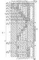
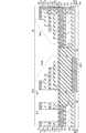
次に、図4を参照して、第1実施形態に係る不揮発性半導体記憶装置100の更に具体的構成を説明する。図4は、第1実施形態に係る不揮発性半導体記憶装置のロウ方向の断面図である。図4に示すように、不揮発性半導体記憶装置100は、上述したメモリトランジスタ領域12、及びそのメモリトランジスタ領域12の周辺に設けられた周辺領域(第2の領域)Phを有する。(Specific Configuration of Nonvolatile
Next, a more specific configuration of the nonvolatile
メモリトランジスタ領域12は、半導体基板Ba上に、順次、ソース側選択トランジスタ層20、メモリトランジスタ層(第1の層)30、及びドレイン側選択トランジスタ層40を有する。ソース側選択トランジスタ層20、メモリトランジスタ層30、及びドレイン側選択トランジスタ層40は、メモリストリングスMSを構成する。 The
ソース側選択トランジスタ層20は、ソース側選択トランジスタSSTrmnとして機能する。メモリトランジスタ層30は、メモリトランジスタMTrmnとして機能する。メモリトランジスタ層30は、電気的に書き換え可能であり且つ直列に接続された複数のメモリセルとして機能する。ドレイン側選択トランジスタ層40は、ドレイン側選択トランジスタSDTrmnとして機能する。 The source side
周辺領域Phは、第1CMP用ダミー層60、及び第2CMP用ダミー層(第2の層)70を有する。第1CMP用ダミー層60は、CMPによるソース側選択トランジスタ層20の平坦化に際して、ソース側選択トランジスタ層20の研磨面を所望の面に平行とするために用いられる層である。第2CMP用ダミー層70は、CMPによるメモリトランジスタ層30の平坦化に際して、メモリトランジスタ層30の研磨面を所望の面に平行とするために用いられる層である。 The peripheral region Ph includes a first
先ず、メモリトランジスタ領域12の構成(ソース側選択トランジスタ層20、メモリトランジスタ層30、及びドレイン側選択トランジスタ層40)について説明する。 First, the configuration of the memory transistor region 12 (source side
メモリトランジスタ領域12において、半導体基板Ba上には、P−型領域(P−Well領域)Ba1が形成されている。また、P−型領域Ba1上には、n+領域(ソース線領域)Ba2が形成されている。 In the
ソース側選択トランジスタ層20は、半導体基板Ba2上に順次積層された、ソース側第1絶縁層21、ソース側導電層22、ソース側第2絶縁層23、及びソース側分離絶縁層24を有する。 The source side
ソース側第1絶縁層21、ソース側導電層22、ソース側第2絶縁層23、及びソース側分離絶縁層24は、半導体基板Baと平行な水平方向においてメモリトランジスタ領域12にて2次元的に広がりを有するように形成されている。ソース側第1絶縁層21、ソース側導電層22、ソース側第2絶縁層23、及びソース側分離絶縁層24は、メモリトランジスタ領域12内の所定領域(消去単位)毎に分断され、それらのロウ方向及びカラム方向の端部には、側壁絶縁層25が形成されている。また、半導体基板Ba上からソース側分離絶縁層24の上面に達するまで、層間絶縁層26が設けられている。 The source side first insulating
ソース側第1絶縁層21、及びソース側第2絶縁層23は、酸化シリコン(SiO2)にて構成されている。ソース側導電層22は、P+型のポリシリコン(p−Si)にて構成されている。ソース側分離絶縁層24は、窒化シリコン(SiN)にて構成されている。側壁絶縁層25、及び層間絶縁層26は、酸化シリコン(SiO2)にて構成されている。The source side first insulating
また、ソース側分離絶縁層24、ソース側第2絶縁層23、ソース側導電層22、及びソース側第1絶縁層21を貫通するようにソース側ホール27が形成されている。ソース側ホール27に面する側壁には、順次、ソース側ゲート絶縁層28、ソース側柱状半導体層29が設けられている。 A source-
ソース側ゲート絶縁層28は、酸化シリコン(SiO2)にて形成されている。ソース側柱状半導体層29は、ポリシリコン(p−Si)にて形成されている。The source side
なお、上記ソース側選択トランジスタ20の構成において、ソース側導電層22の構成を換言すると、ソース側導電層22は、ソース側柱状半導体層29と共にソース側ゲート絶縁層28を挟むように形成されている。 In the configuration of the source side
また、ソース側選択トランジスタ層20において、ソース側導電層22が、ソース側選択ゲート線SGSとして機能する。また、ソース側導電層22が、ソース側選択トランジスタSSTrmnの制御ゲートとして機能する。 In the source side
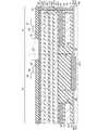
メモリトランジスタ層30は、ソース側分離絶縁層24の上方及び層間絶縁層26の上方に設けられた第1〜第5ワード線間絶縁層31a〜31eと、第1〜第5ワード線間絶縁層31a〜31eの上下間に設けられた第1〜第4ワード線導電層32a〜32d(複数の第1導電層)と、第5ワード線間絶縁層31e上に順次積層されたメモリ分離絶縁層33及びメモリ保護絶縁層(第1絶縁層)34を有する。 The
第1〜第5ワード線間絶縁層31a〜31e、第1〜第4ワード線導電層32a〜32d、及びメモリ分離絶縁層33は、ロウ方向及びカラム方向においてメモリトランジスタ領域12にて2次元的に広がりを有するように形成されている。第1〜第5ワード線間絶縁層31a〜31e、第1〜第4ワード線導電層32a〜32d、及びメモリ分離絶縁層33は、図4の符号「Sta1」に示すように、ロウ方向の端部で階段状に形成されている。メモリ保護絶縁層34は、第1〜第5ワード線間絶縁層31a〜31e、第1〜第4ワード線導電層32a〜32d、及びメモリ分離絶縁層33のロウ方向の端部及びカラム方向の端部を覆うように、それら第1〜第5ワード線間絶縁層31a〜31e、第1〜第4ワード線導電層32a〜32d、及びメモリ分離絶縁層33に亘って連続して形成されている。また、第1ワード線間絶縁層31aの上面に形成されたメモリ保護絶縁層34の上面から、メモリ分離絶縁層33の上面に形成されたメモリ保護絶縁層34の上面まで、層間絶縁層35が形成されている。 The first to fifth inter-wordline insulating
第1〜第5ワード線間絶縁層31a〜31eは、酸化シリコン(SiO2)にて構成されている。第1〜第4ワード線導電層32a〜32dは、P+型のポリシリコン(p−Si)にて構成されている。メモリ分離絶縁層33、及びメモリ保護絶縁層34は、窒化シリコン(SiN)にて構成されている。層間絶縁層35は、酸化シリコン(SiO2)にて構成されている。The first to fifth inter-wordline insulating
また、メモリトランジスタ層30において、メモリ分離絶縁層33、第1〜第5ワード線間絶縁層31a〜31e、及び第1〜第4ワード線導電層32a〜32dを貫通するようにメモリホール36が形成されている。メモリホール36は、ソース側ホール27と整合する位置に設けられている。メモリホール36内の側壁には、順次、メモリゲート絶縁層37、及びメモリ柱状半導体層(第1半導体層)38が設けられている。 In the
メモリゲート絶縁層37は、図5に示すように構成されている。図5は、図4に示すメモリトランジスタ層30の拡大図である。図5に示すように、メモリゲート絶縁層37は、メモリ柱状半導体層38の側壁から、順次、トンネル絶縁層37a、電荷を蓄積する電荷蓄積層37b、及びブロック絶縁層37cを有する。 The memory
トンネル絶縁層37a、及びブロック絶縁層37cは、酸化シリコン(SiO2)にて形成されている。電荷蓄積層37bは、窒化シリコン(SiN)にて形成されている。メモリ柱状半導体層38は、ポリシリコン(p−Si)にて構成されている。また、メモリ柱状半導体層38は、その上部をN+型のポリシリコンにて構成されたものであってもよい。The
なお、上記メモリトランジスタ30において、第1〜第4ワード線導電層32a〜32dの構成を換言すると、第1〜第4ワード線導電層32a〜32dは、メモリ柱状半導体層38と共にトンネル絶縁層37a、電荷蓄積層37b及びブロック絶縁層37cを挟むように形成されている。また、メモリ柱状半導体層38は、ソース側柱状半導体層29の上面、及び後述するドレイン側柱状半導体層48の下面に接するように形成されている。 In other words, in the
また、メモリトランジスタ層30において、第1〜第4ワード線導電層32a〜32dが、ワード線WL1〜WL4として機能する。また、第1〜第4ワード線導電層32a〜32dが、メモリトランジスタMTrmnの制御ゲートとして機能する。 In the
ドレイン側選択トランジスタ層40は、メモリ保護絶縁層34上に順次積層されたドレイン側第1絶縁層41、ドレイン側導電層42、ドレイン側第2絶縁層43、及びドレイン側分離絶縁層44を有する。 The drain side
ドレイン側第1絶縁層41、ドレイン側導電層42、ドレイン側第2絶縁層43、及びドレイン側分離絶縁層44は、メモリ柱状半導体層38の上部に整合する位置に設けられ且つロウ方向に延びカラム方向に繰り返し設けられたライン状に形成されている。また、層間絶縁層35の上面及びメモリ保護絶縁層34の上面から、ドレイン側分離絶縁層44の上方の所定高さまで層間絶縁層45が形成されている。 The drain-side first insulating
ドレイン側第1絶縁層41及びドレイン側第2絶縁層43は、酸化シリコン(SiO2)にて形成されている。ドレイン側導電層42は、P+型のポリシリコン(p−Si)にて形成されている。ドレイン側分離絶縁層44は、窒化シリコン(SiN)にて形成されている。層間絶縁層45は、酸化シリコン(SiO2)にて形成されている。The drain side first insulating
また、ドレイン側選択トランジスタ層40において、ドレイン側分離絶縁層44、ドレイン側第2絶縁層43、ドレイン側導電層42、ドレイン側第1絶縁層41及び、メモリ保護絶縁層34を貫通するようにドレイン側ホール46が形成されている。ドレイン側ホール46は、メモリホール36と整合する位置に設けられている。ドレイン側ホール46に面する側壁には、順次、ドレイン側ゲート絶縁層47、及びドレイン側柱状半導体層48が設けられている。 In the drain side
ドレイン側ゲート絶縁層47は、酸化シリコン(SiO2)にて形成されている。ドレイン側柱状半導体層48は、ポリシリコン(p−Si)にて形成されている。また、ドレイン側柱状半導体層48の上部は、N+型ポリシリコンにて構成されている。The drain side
なお、上記ドレイン側選択トランジスタ40の構成において、ドレイン側導電層42の構成を換言すると、ドレイン側導電層42は、ドレイン側柱状半導体層48と共にドレイン側ゲート絶縁層47を挟むように形成されている。また、ドレイン側柱状半導体層48は、メモリ柱状半導体層38の上面に接するように形成されている。 In the configuration of the drain side
また、ドレイン側選択トランジスタ40において、ドレイン側導電層42が、ドレイン側選択ゲート線SGDとして機能する。また、ドレイン側導電層42が、ドレイン側選択トランジスタSDTrmnの制御ゲートとして機能する。 In the drain side
さらに、上記ソース側選択トランジスタ層20、メモリトランジスタ層30、及びドレイン側選択トランジスタ層40においては、上面からコンタクトホール51a〜51hが形成されている。 Further, in the source side
コンタクトホール51aは、上面からn+領域Ba2に達するように形成されている。コンタクトホール51bは、ソース側導電層22の上面に達するように形成されている。コンタクトホール51c〜51fは、第1〜第4ワード線導電層32a〜32dの上面に達するように形成されている。コンタクトホール51gは、ドレイン側導電層42の上面に達するように形成されている。コンタクトホール51hは、ドレイン側柱状半導体層48の上面に達するように形成されている。
コンタクトホール51a〜51h内には、接続導電層54が形成されている。接続導電層54は、メモリトランジスタ層30の上層から下層に延びるように形成されている。接続導電層54は、バリアメタル層52、及びメタル層53を有する。バリアメタル層52は、コンタクトホール51a〜51hに面する側壁に形成されている。メタル層53は、バリアメタル層52の側壁に接するように形成されている。バリアメタル層52は、チタン(Ti)/窒化チタン(TiN)にて構成されている。メタル層53は、タングステン(W)にて構成されている。 A connection
次に、周辺領域Ph(第1CMP用ダミー層60、及び第2CMP用ダミー層70)の構成にてついて説明する。 Next, the configuration of the peripheral region Ph (the first
周辺領域Phにおける半導体基板Baのメモリトランジスタ領域12側には、素子分離絶縁層Ba3が形成されている。なお、半導体基板Ba上には、メモリトランジスタ領域12と同様に、P−型領域Ba1、及びn+領域Ba2が設けられている。 On the
第1CMP用ダミー層60は、半導体基板Ba上に順次積層された、ダミーソース側第1絶縁層61、ダミーソース側導電層62、ダミーソース側第2絶縁層63、及びダミーソース側分離絶縁層64を有する。 The first
ダミーソース側第1絶縁層61、ダミーソース側導電層62、ダミーソース側第2絶縁層63、及びダミーソース側分離絶縁層64は、半導体基板Baと平行な水平方向において周辺領域Phにて2次元的に広がりを有するように形成されている。ダミーソース側第1絶縁層61、ダミーソース側導電層62、ダミーソース側第2絶縁層63、及びダミーソース側分離絶縁層64のロウ方向及びカラム方向の端部には、側壁絶縁層65が形成されている。また、半導体基板Ba上からダミーソース側分離絶縁層64の上面に達するまで、層間絶縁層66が設けられている。 The dummy source side first insulating
ダミーソース側第1絶縁層61は、ソース側第1絶縁層21と同層に形成されている。ダミーソース側導電層62は、ソース側導電層22と同層に形成されている。ダミーソース側第2絶縁層63は、ソース側第2絶縁層23と同層に形成されている。ダミーソース側分離絶縁層64は、ソース側分離絶縁層24と同層に形成されている。層間絶縁層66は、メモリトランジスタ領域12の層間絶縁層26と一体に連続して形成されている。換言すると、層間絶縁層66は、メモリトランジスタ領域12の層間絶縁層26と同層に形成されている。 The dummy source side first insulating
ダミーソース側第1絶縁層61、及びダミーソース側第2絶縁層63は、酸化シリコン(SiO2)にて構成されている。ダミーソース側導電層62は、P+型のポリシリコン(p−Si)にて構成されている。ダミーソース側分離絶縁層64は、窒化シリコン(SiN)にて構成されている。側壁絶縁層65、及び層間絶縁層66は、酸化シリコン(SiO2)にて構成されている。The dummy source side first insulating
上記のダミーソース側導電層62は、例えば、周辺領域Phに設けられた高耐圧MOSトランジスタのゲートとして機能する。なお、図4において、当該高耐圧MOSトランジスタのソース・ドレイン等は、図示を省略している。 The dummy source side
第2CMP用ダミー層70は、ダミー第1〜第5ワード線間絶縁層71a〜71e、ダミー第1〜第5ワード線間絶縁層71a〜71eの上下間に設けられたダミー第1〜第4ワード線導電層(第2導電層)72a〜72d、ダミー第5ワード線間絶縁層71e上に順次積層されたダミーメモリ分離絶縁層73及びダミーメモリ保護絶縁層(第2絶縁層)74を有する。 The second
ダミー第1〜第5ワード線間絶縁層71a〜71e、ダミー第1〜第4ワード線導電層72a〜72d、及びダミーメモリ分離絶縁層73は、ロウ方向及びカラム方向において周辺領域Phにて2次元的に広がりを有するように形成され、図4の符号「Sta2」に示すように、メモリトランジスタ層30側のロウ方向の端部で階段状に形成されている。ダミーメモリ保護絶縁層74は、ダミー第1〜第5ワード線間絶縁層71a〜71e、ダミー第1〜第4ワード線導電層72a〜72d、及びダミーメモリ分離絶縁層74のロウ方向の端部及びカラム方向の端部を覆うように、それらダミー第1〜第5ワード線間絶縁層71a〜71e、ダミー第1〜第4ワード線導電層72a〜72d、及びダミーメモリ分離絶縁層74に亘って連続して形成されている。また、ダミー第1ワード線間絶縁層71aの上面に形成されたダミーメモリ保護絶縁層74の上面から、ダミーメモリ分離絶縁層73の上面に形成されたダミーメモリ保護絶縁層74の上面まで、層間絶縁層75が形成されている。 The dummy first to fifth inter-word
また、第2CMP用ダミー層70(層間絶縁層75)の上面及びダミーメモリ保護絶縁層74の上面から所定高さまで、層間絶縁層76が形成されている。 An interlayer insulating
ダミー第1ワード線間絶縁層71aは、第1ワード線間絶縁層31aと一体に連続して形成されている。ダミー第1ワード線間絶縁層71aは、第1ワード線間絶縁層31aと同層に形成されている。ダミー第2〜第5ワード線間絶縁層71b〜71eは、第2〜第5ワード線間絶縁層31b〜31eと同層に形成されている。ダミーメモリ分離絶縁層73は、メモリ分離絶縁層33と同層に形成されている。ダミーメモリ保護絶縁層74は、メモリ保護絶縁層34と一体に連続して形成されている。 The dummy first inter-word
層間絶縁層75は、メモリトランジスタ領域12に設けられた層間絶縁層35と一体に連続して形成されている。層間絶縁層76は、メモリトランジスタ領域12に設けられた層間絶縁層45と一体に連続して形成されている。 The interlayer insulating
ダミー第1〜第5ワード線間絶縁層71a〜71eは、酸化シリコン(SiO2)にて構成されている。ダミー第1〜第4ワード線導電層72a〜72dは、P+型のポリシリコン(p−Si)にて構成されている。ダミーメモリ分離絶縁層73、及びダミーメモリ保護絶縁層74は、窒化シリコン(SiN)にて構成されている。層間絶縁層75、76は、酸化シリコン(SiO2)にて構成されている。The dummy first to fifth inter-wordline insulating
また、第2CMP用ダミー層70の配線領域Ar1には、ダミー第1〜第5ワード線間絶縁層71a〜71e、ダミー第1〜第4ワード線導電層72a〜72d、ダミーメモリ分離絶縁層73、及びダミーメモリ保護絶縁層74を貫通するように、ホール77(第1の貫通孔)が形成されている。ホール77内には、ホール内絶縁層78が設けられている(満たされている)。ホール内絶縁層78は、酸化シリコン(SiO2)にて構成されている。なお、配線領域Ar1は、後述する接続導電層84が設けられる領域である。In addition, in the wiring region Ar1 of the second
さらに、上記第1CMP用ダミー層60、第2CMP用ダミー層70においては、上面からコンタクトホール(第2の貫通孔)81a、81bが形成されている。 Further, in the first
コンタクトホール(第2の貫通孔)81aは、n+領域Ba2に達するように形成されている。コンタクトホール81aは、層間絶縁層76、ホール内絶縁層78、ダミー第1ワード線間絶縁層71a、及び層間絶縁層66を貫通するように形成されている。 The contact hole (second through hole) 81a is formed so as to reach the n + region Ba2. The
コンタクトホール81b(第2の貫通孔)は、ダミーソース側導電層62の上面に達するように形成されている。コンタクトホール81bは、層間絶縁層76、ホール内絶縁層78、ダミー第1ワード線間絶縁層71a、ダミーソース側分離絶縁層64、及びダミーソース側第2絶縁層63を貫通するように形成されている。 The
コンタクトホール81a、81b内には、接続導電層84が形成されている。接続導電層84は、第2CMP用ダミー層70の上層から下層へと延びるように形成されている。接続導電層84は、バリアメタル層82、及びメタル層83を有する。バリアメタル層82は、コンタクトホール81a、81bに面する側壁に形成されている。メタル層83は、バリアメタル層82の側壁に接するように形成されている。バリアメタル層82は、チタン(Ti)/窒化チタン(TiN)にて構成されている。メタル層83は、タングステン(W)にて構成されている。 A connection
上記構成を換言すると、ダミー第1〜第4ワード線導電層72a〜72dの端部は、第2CMP用ダミー層70の上層から下層へと延びる接続導電層84が設けられる配線領域(所定領域)Ar1にて半導体基板Baに対して略垂直方向に延びる直線に沿って揃うように形成されている。ここで、「略垂直」とは、具体的には、85°〜91°程度を想定するが、厳密なものではない。「揃う」の意味も同様であり、ある程度の凹凸を有するものも含む。 In other words, the end portions of the dummy first to fourth word line
(第1実施形態に係る不揮発性半導体記憶装置100の製造工程)
次に、図6〜図17を参照して、第1実施形態に係る不揮発性半導体記憶装置100の製造工程について説明する。(Manufacturing process of the nonvolatile
A manufacturing process of the nonvolatile
先ず、半導体基板Ba上にソース側選択トランジスタ層20、及び第1CMP用ダミー層60を形成する。続いて、それらソース側選択トランジスタ層20、及び第1CMP用ダミー層60の上に、第1〜第5板状絶縁層31a’〜31e’、及び第1〜第4板状導電層(導電層)32a’〜32d’を交互に堆積させた後、板状分離絶縁層33’を堆積させる。次に、メモリトランジスタ領域12において、第1〜第5板状絶縁層31a’〜31e’、第1〜第4板状導電層32a’〜32d’、及び板状分離絶縁層33’を貫通するように、メモリホール36を形成する。そして、メモリホール36内にメモリゲート絶縁層37及びメモリ柱状半導体層38を形成する。以上の工程を経て、図6に示す積層構造が形成される。 First, the source side
次に、図7に示すように、板状分離絶縁層33’上であって、メモリトランジスタ領域12と周辺領域Phとの境界となる領域Ar2を除いて、レジスト101を形成する。ここで、例えば、レジスト101は、約3μmの厚みで形成する。続いて、レジスト101をマスクとして、エッチングを行う。次に、矢印A1〜A3、矢印B1〜B3に示す方向にレジスト101をスリミングしながら、レジスト101をマスクとしてエッチングを行う。なお、上記エッチングの後、レジスト101を除去する。 Next, as shown in FIG. 7, a resist 101 is formed on the plate-like isolation /
上記の図7に示す工程を経て、図8に示す積層構造が形成される。すなわち、第1〜第5板状絶縁層31a’〜31e’は、メモリトランジスタ領域12において2次元的に広がりを有する第1〜第5ワード線間絶縁層31a〜31eとなる。第1〜第4板状導電層32a’〜32d’は、メモリトランジスタ領域12において2次元的に広がりを有する第1〜第4ワード線導電層32a〜32dとなる。板状分離絶縁層33’は、メモリトランジスタ領域12において2次元的に広がりを有するメモリ分離絶縁層33となる。また、図7に示す工程により、第1〜第5ワード線間絶縁層31a〜31e、第1〜第4ワード線導電層32a〜32d、及びメモリ分離絶縁層33は、ロウ方向の端部で階段状に形成される(図8の符号「Sta1」参照)。 The laminated structure shown in FIG. 8 is formed through the steps shown in FIG. That is, the first to fifth plate-like insulating
同様に、第1〜第5板状絶縁層31a’〜31e’は、周辺領域Phにおいて2次元的に広がりを有するダミー第1〜第5ワード線間絶縁層71a〜71eとなる。第1〜第4板状導電層32a’〜32d’は、周辺領域Phにおいて2次元的に広がりを有するダミー第1〜第4ワード線導電層72a〜72dとなる。板状分離絶縁層33’は、周辺領域Phにおいて2次元的に広がりを有するダミーメモリ分離絶縁層73となる。また、図7に示す工程により、ダミー第1〜第5ワード線間絶縁層71a〜71e、ダミー第1〜第4ワード線導電層72a〜72d、及びダミーメモリ分離絶縁層73は、メモリトランジスタ層30側のロウ方向の端部で階段状に形成される(図8の符号「Sta2」参照)。 Similarly, the first to fifth plate-like insulating
続いて、図9に示すように、窒化シリコン(SiN)を堆積させ、メモリ保護絶縁層34、及びダミーメモリ保護絶縁層74を形成する。なお、メモリ保護絶縁層34及びダミーメモリ保護絶縁層74は、一体に形成される。メモリ保護絶縁層34は、第1〜第5ワード線間絶縁層31a〜31e、第1〜第4ワード線導電層32a〜32d、メモリ分離絶縁層33を覆うように形成される。また、ダミーメモリ保護絶縁層74は、第1〜第5ワード線間絶縁層71a〜71e、ダミー第1〜第4ワード線導電層72a〜72d、及びダミーメモリ分離絶縁層73を覆うように形成される。 Subsequently, as shown in FIG. 9, silicon nitride (SiN) is deposited, and the memory
次に、図10に示すように、レジスト102を形成する。レジスト102は、配線領域Ar1となる領域を除いて、メモリ保護絶縁層34及びダミーメモリ保護絶縁層74上に形成する。 Next, as shown in FIG. 10, a resist 102 is formed. The resist 102 is formed on the memory
続いて、図11に示すように、レジスト102をマスクとして、ダミー第2〜第5ワード線間絶縁層71b〜71e、ダミー第1〜第4ワード線導電層72a〜72d、ダミーメモリ分離絶縁層73、及びダミーメモリ保護絶縁層74を貫通するように、配線領域Ar1にホール(第1の貫通孔)77を形成する。ホール77の形成後、レジスト102を除去する。 Subsequently, as shown in FIG. 11, using the resist 102 as a mask, dummy second to fifth word
次に、図12に示すように、酸化シリコン(SiO2)を堆積させ、CMPを行い、層間絶縁層35、75、ホール内絶縁層78を形成する。なお、層間絶縁層35及び層間絶縁層75は、一体に形成される。図12に示す工程にて、層間絶縁層35は、第1ワード線間絶縁層31a上のメモリ保護絶縁層34の上面からメモリ分離絶縁層33上のメモリ保護絶縁層34の上面まで形成される。層間絶縁層75は、ダミー第1ワード線間絶縁層71a上のダミーメモリ保護絶縁層74の上面からダミーメモリ分離絶縁層73上のダミーメモリ保護絶縁層74の上面まで形成される。ホール内絶縁層78は、配線領域Ar1にてホール77を埋めるように形成される。Next, as shown in FIG. 12, silicon oxide (SiO2 ) is deposited and CMP is performed to form interlayer insulating
上記図12に示す工程において、メモリ保護絶縁層34は、CMPのストッパーとして機能する。同様に、ダミーメモリ保護絶縁層74は、CMPによるメモリトランジスタ層30の平坦化に際して、メモリトランジスタ層30の研磨面を所望の面に平行とするために用いられるストッパーとして機能する。 In the process shown in FIG. 12, the memory
続いて、図13に示すように、メモリトランジスタ領域12の所定領域内のメモリ保護絶縁層34上に酸化シリコン(SiO2)、ポリシリコン(p−Si)、酸化シリコン(SiO2)、窒化シリコン(SiN)を堆積させる。上記工程により、メモリトランジスタ領域12の所定領域内のメモリ保護絶縁層34上に、ドレイン側第1絶縁層41、ドレイン側導電層42、ドレイン側第2絶縁層43、及びドレイン側分離絶縁層44が形成される。Subsequently, as shown in FIG. 13, silicon oxide (SiO2 ), polysilicon (p-Si), silicon oxide (SiO2 ), silicon nitride is formed on the memory
次に、図14に示すように、メモリ保護絶縁層34、ドレイン側第1絶縁層41、ドレイン側導電層42、ドレイン側第2絶縁層43、及びドレイン側分離絶縁層44を貫通するように、ドレイン側ホール46を形成する。ドレイン側ホール46は、メモリホール36と整合する位置に形成する。 Next, as shown in FIG. 14, the memory
続いて、図15に示すように、ドレイン側ホール46に面するメモリ保護絶縁層34、ドレイン側第1絶縁層41、ドレイン側導電層42、ドレイン側第2絶縁層43、及びドレイン側分離絶縁層44の側壁に、酸化シリコン、及びポリシリコンを堆積させ、ドレイン側ゲート絶縁層47、及びドレイン側柱状半導体層48を形成する。 Subsequently, as shown in FIG. 15, the memory
次に、図16に示すように、酸化シリコン(SiO2)を堆積させ、メモリトランジスタ領域12に層間絶縁層45を形成し、周辺領域Phに層間絶縁層76を形成する。なお、層間絶縁層45及び層間絶縁層76は、一体に形成される。Next, as shown in FIG. 16, silicon oxide (SiO2 ) is deposited, an
続いて、図17に示すように、メモリトランジスタ領域12にコンタクトホール51a〜51hを形成する。コンタクトホール51aは、n+領域Ba2に達するように形成する。コンタクトホール51bは、ソース側導電層22に達するように形成する。コンタクトホール51c〜51fは、第1〜第4ワード線導電層32a〜32dに達するように形成する。コンタクトホール51gは、ドレイン側導電層42の上面に達するように形成する。コンタクトホール51hは、ドレイン側柱状半導体層48の上面に達するように形成する。 Subsequently, as shown in FIG. 17, contact holes 51 a to 51 h are formed in the
また、図17に示すように、周辺領域Phにコンタクトホール(第2の貫通孔)81a、81bを形成する。コンタクトホール81aは、n+領域Ba2に達するように形成する。コンタクトホール81aは、層間絶縁層76、ホール内絶縁層78、ダミー第1ワード線間絶縁層71a、及び層間絶縁層66を貫通するように形成する。コンタクトホール81bは、ダミーソース側導電層62に達するように形成する。コンタクトホール81bは、層間絶縁層76、ホール内絶縁層78、ダミー第1ワード線間絶縁層71a、ダミーソース側分離絶縁層64、及びダミーソース側第2絶縁層63を貫通するように形成する。 As shown in FIG. 17, contact holes (second through holes) 81a and 81b are formed in the peripheral region Ph. The
図17に示す工程に引き続き、メモリトランジスタ領域12において、コンタクトホール51a〜51gにチタン(Ti)/窒化チタン(TiN)、及びタングステン(W)を堆積させ、CMPを行い、接続導電層54(バリアメタル層52、及びメタル層53)を形成する。同時に、周辺領域Phにおいて、コンタクトホール81a、81bにチタン(Ti)/窒化チタン(TiN)、及びタングステン(W)を堆積させた後、CMPが行われ、接続導電層84(バリアメタル層82、及びメタル層83)が形成される。上記工程を経て、図4に示す不揮発性半導体記憶装置100が形成される。 Subsequent to the step shown in FIG. 17, in the
(第1実施形態に係る不揮発性半導体記憶装置100の効果)
次に、第1実施形態に係る不揮発性半導体記憶装置100の効果について説明する。上記のように第1実施形態に係る不揮発性半導体記憶装置100において、メモリトランジスタ層30の第1〜第4ワード線導電層32a〜32dのロウ方向の端部は、階段状に形成されている。一方、第2CMP用ダミー層70のダミー第1〜第4ワード線導電層72a〜72dの端部は、配線領域Ar1にて半導体基板Baに対して略垂直方向に延びる直線に沿って揃うように形成されている。(Effect of Nonvolatile
Next, effects of the nonvolatile
ここで、第1実施形態の効果を説明するための比較例を考える。比較例に係る不揮発性半導体記憶装置において、ダミー第1〜第4ワード線導電層の端部は、配線領域にて階段状に形成されているものとする。 Here, consider a comparative example for explaining the effect of the first embodiment. In the nonvolatile semiconductor memory device according to the comparative example, it is assumed that the end portions of the dummy first to fourth word line conductive layers are formed stepwise in the wiring region.
上記比較例と第1実施形態とを比較すると、ダミー第1〜第4ワード線導電層72a〜72dの端部形状により、第1実施形態における配線領域Ar1は、比較例における配線領域よりも、その占有面積を縮小化することができる。従って、第1実施形態に係る不揮発性半導体記憶装置100に係る第2CMP用ダミー層70は、比較例よりもその占有面積を縮小化することができる。すなわち、第1実施形態に係る不揮発性半導体記憶装置100は、その占有面積を比較例よりも縮小化することができる。また、第2CMP用ダミー層70は、比較例よりもそのパターン配置の自由度を向上させることができる。 Comparing the comparative example with the first embodiment, due to the end shape of the dummy first to fourth word line
[第2実施形態]
(第2実施形態に係る不揮発性半導体記憶装置100aの具体的構成)
次に、図18を参照して、第2実施形態に係る不揮発性半導体記憶装置100aの具体的構成を説明する。図18は、第2実施形態に係る不揮発性半導体記憶装置100aのロウ方向の断面図である。なお、第2実施形態において、第1実施形態と同様の構成については、同一符号を付し、その説明を省略する。[Second Embodiment]
(Specific Configuration of Nonvolatile
Next, a specific configuration of the nonvolatile
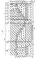
図18に示すように、不揮発性半導体記憶装置100aは、第1実施形態と異なる周辺領域Phaを有する。周辺領域Phaは、第1実施形態と異なる第2CMP用ダミー層70aを有する。 As shown in FIG. 18, the nonvolatile
第2CMP用ダミー層70aは、第1実施形態と異なるダミーメモリ保護絶縁層74aを有する。ダミーメモリ保護絶縁層74aは、第1実施形態と異なり、ホール77に面するダミー第1〜第5ワード線間絶縁層71a〜71eの側壁、ダミー第1〜第4ワード線導電層72a〜72dの側壁、及びダミーメモリ分離絶縁層73の側壁、ホール77の底部に亘って連続して形成されている。 The second
(第2実施形態に係る不揮発性半導体記憶装置100aの製造工程)
次に、図19〜図24を参照して、第2実施形態に係る不揮発性半導体記憶装置100aの製造工程について説明する。(Manufacturing Process of Nonvolatile
Next, with reference to FIGS. 19 to 24, a manufacturing process of the nonvolatile
先ず、第1実施形態の図6に示す工程まで行う。続いて、図19に示すように、レジスト103を形成する。レジスト103は、配線領域Ar1となる領域を除いて、板状分離絶縁層33’上に形成する。 First, the steps up to the step shown in FIG. 6 of the first embodiment are performed. Subsequently, a resist 103 is formed as shown in FIG. The resist 103 is formed on the plate-like isolation / insulation layer 33 'except for the region to be the wiring region Ar1.
続いて、図20に示すように、レジスト103をマスクとして、エッチングを行う。なお、エッチングの後、レジスト103を除去する。この図20に示す工程により、ホール77が形成される。 Subsequently, as shown in FIG. 20, etching is performed using the resist 103 as a mask. Note that the resist 103 is removed after the etching. A
次に、図21に示すように、板状分離絶縁層33’上であって、メモリトランジスタ領域12と周辺領域Phとの境界となる領域Ar2を除いて、レジスト104を形成する。ここで、例えば、レジスト104は、約3μmの厚みで形成する。続いて、レジスト104をマスクとして、エッチングを行う。次に、矢印C1〜C3、矢印D1〜D3に示す方向にレジスト104をスリミングしながら、レジスト104をマスクとしてエッチングを行う。なお、上記エッチングの後、レジスト104を除去する。 Next, as shown in FIG. 21, a resist 104 is formed on the plate-like
上記の図21に示す工程を経て、図22に示す積層構造が形成される。すなわち、第1〜第5板状絶縁層31a’〜31e’は、第1〜第5ワード線間絶縁層31a〜31eとなる。第1〜第4板状導電層32a’〜32d’は、第1〜第4ワード線導電層32a〜32dとなる。板状分離絶縁層33’は、メモリ分離絶縁層33となる。また、図21に示す工程により、第1〜第5ワード線間絶縁層31a〜31e、第1〜第4ワード線導電層32a〜32d、及びメモリ分離絶縁層33は、ロウ方向の端部で階段状に形成される(図22の符号「Sta1」参照)。 The laminated structure shown in FIG. 22 is formed through the steps shown in FIG. That is, the first to fifth plate-like insulating
同様に、第1〜第5板状絶縁層31a’〜31e’は、ダミー第1〜第5ワード線間絶縁層71a〜71eとなる。第1〜第4板状導電層32a’〜32d’は、ダミー第1〜第4ワード線導電層72a〜72dとなる。板状分離絶縁層33’は、ダミーメモリ分離絶縁層73となる。また、図21に示す工程により、ダミー第1〜第5ワード線間絶縁層71a〜71e、ダミー第1〜第4ワード線導電層72a〜72d、及びダミーメモリ分離絶縁層73は、メモリトランジスタ層30側のロウ方向の端部で階段状に形成される(図22の符号「Sta2」参照)。 Similarly, the first to fifth plate-like insulating
続いて、図23に示すように、窒化シリコン(SiN)を堆積させ、メモリ保護絶縁層34、及びダミーメモリ保護絶縁層74aを形成する。なお、メモリ保護絶縁層34及びダミーメモリ保護絶縁層74aは、一体に形成される。ここで、ダミーメモリ保護絶縁層74aは、ホール77に面するダミー第1〜第5ワード線間絶縁層71a〜71eの側壁、ダミー第1〜第4ワード線導電層72a〜72dの側壁、及びダミーメモリ分離絶縁層73の側壁、ホール77の底部に亘って連続して形成される。 Subsequently, as shown in FIG. 23, silicon nitride (SiN) is deposited to form the memory
次に、図24に示すように、酸化シリコン(SiO2)を堆積させ、CMPを施し、層間絶縁層35、75、及びホール内絶縁層78を形成する。上記図24に示す工程において、メモリ保護絶縁層34は、CMPのストッパーとして機能する。同様に、ダミーメモリ保護絶縁層74aは、CMPによるメモリトランジスタ層30の平坦化に際して、メモリトランジスタ層30の研磨面を所望の面に平行とするために用いられるストッパーとして機能する。Next, as shown in FIG. 24, silicon oxide (SiO2 ) is deposited and subjected to CMP to form interlayer insulating
図24に示す工程において、層間絶縁層35は、第1ワード線間絶縁層31a上のメモリ保護絶縁層34の上面からメモリ分離絶縁層33上のメモリ保護絶縁層34の上面まで形成される。また、層間絶縁層75は、ダミー第1ワード線間絶縁層71a上のダミーメモリ保護絶縁層74aの上面からダミーメモリ分離絶縁層73上のダミーメモリ保護絶縁層74aの上面まで形成される。また、ホール内絶縁層78は、ホール77を埋めるように形成される。 In the step shown in FIG. 24, the
図24に続いて、第1実施形態の図13〜図17に工程を行い、第2実施形態に係る不揮発性半導体記憶装置100aを形成する。 Subsequent to FIG. 24, steps are performed in FIGS. 13 to 17 of the first embodiment to form the nonvolatile
(第2実施形態に係る不揮発性半導体記憶装置100aの効果)
次に、第2実施形態に係る不揮発性半導体記憶装置100aの効果について説明する。第2実施形態に係る不揮発性半導体記憶装置100aは、第1実施形態と略同様の構成を有する。したがって、第2実施形態に係る不揮発性半導体記憶装置100aは、第1実施形態と同様の効果を奏する。(Effect of Nonvolatile
Next, effects of the nonvolatile
[第3実施形態]
(第3実施形態に係る不揮発性半導体記憶装置100bの具体的構成)
次に、図25を参照して、第3実施形態に係る不揮発性半導体記憶装置100bの具体的構成について説明する。図25は、第3実施形態に係る不揮発性半導体記憶装置100bのロウ方向の断面図である。なお、第3実施形態において、第1及び第2実施形態と同様の構成については、同一符号を付し、その説明を省略する。[Third Embodiment]
(Specific Configuration of Nonvolatile
Next, a specific configuration of the nonvolatile
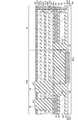
図25に示すように、不揮発性半導体記憶装置100bは、第1及び第2実施形態と異なる周辺領域Phbを有する。周辺領域Phbは、第1及び第2実施形態と異なる第2CMP用ダミー層70bを有する。 As shown in FIG. 25, the nonvolatile
第2CMP用ダミー層70bは、第1及び第2実施形態と異なるダミーメモリ保護絶縁層74bを有する。ダミーメモリ保護絶縁層74bは、第1及び第2実施形態と異なりホール77内に形成されたホール内絶縁層78の上面を覆うように形成されている。 The second
(第3実施形態に係る不揮発性半導体記憶装置100bの製造工程)
次に、図26〜図30を参照して、第3実施形態に係る不揮発性半導体記憶装置100bの製造工程について説明する。(Manufacturing process of the nonvolatile
Next, with reference to FIGS. 26 to 30, a manufacturing process of the nonvolatile
先ず、第2実施形態の図20に示す工程まで行う。続いて、図26に示すように、酸化シリコン(SiO2)を堆積させ、ホール77内にホール内絶縁層78を形成する。First, the steps up to the step shown in FIG. 20 of the second embodiment are performed. Subsequently, as shown in FIG. 26, silicon oxide (SiO2 ) is deposited, and an in-
次に、図27に示すように、板状分離絶縁層33’及びホール内絶縁層78上であって、メモリトランジスタ領域12と周辺領域Phとの境界となる領域Ar2を除いて、レジスト105を形成する。ここで、例えば、レジスト105は、約3μmの厚みで形成する。続いて、レジスト105をマスクとして、エッチングを行う。次に、矢印E1〜E3、矢印F1〜F3に示す方向にレジスト105をスリミングしながら、レジスト105をマスクとしてエッチングを行う。なお、上記エッチングの後、レジスト105を除去する。 Next, as shown in FIG. 27, the resist 105 is formed on the plate-like
上記の図27に示す工程を経て、図28に示す積層構造が形成される。すなわち、第1〜第5板状絶縁層31a’〜31e’は、第1〜第5ワード線間絶縁層31a〜31eとなる。第1〜第4板状導電層32a’〜32d’は、第1〜第4ワード線導電層32a〜32dとなる。板状分離絶縁層33’は、メモリ分離絶縁層33となる。また、図27に示す工程により、第1〜第5ワード線間絶縁層31a〜31e、第1〜第4ワード線導電層32a〜32d、及びメモリ分離絶縁層33は、ロウ方向の端部で階段状に形成される(図28の符号「Sta1」参照)。 The laminated structure shown in FIG. 28 is formed through the steps shown in FIG. That is, the first to fifth plate-like insulating
同様に、図27に示す工程を経て、第1〜第5板状絶縁層31a’〜31e’は、ダミー第1〜第5ワード線間絶縁層71a〜71eとなる。第1〜第4板状導電層32a’〜32d’は、ダミー第1〜第4ワード線導電層72a〜72dとなる。板状分離絶縁層33’は、ダミーメモリ分離絶縁層73となる。また、図27に示す工程により、ダミー第1〜第5ワード線間絶縁層71a〜71e、ダミー第1〜第4ワード線導電層72a〜72d、及びダミーメモリ分離絶縁層73は、メモリトランジスタ層30側のロウ方向の端部で階段状に形成される(図28の符号「Sta2」参照)。 Similarly, through the steps shown in FIG. 27, the first to fifth plate-like insulating
続いて、図29に示すように、窒化シリコン(SiN)を堆積させ、メモリ保護絶縁層34、及びダミーメモリ保護絶縁層74bを形成する。なお、メモリ保護絶縁層34、及びダミーメモリ保護絶縁層74bは、一体に形成される。ダミーメモリ保護絶縁層74bは、ホール77内に形成されたホール内絶縁層78の上面を覆うように形成される。 Subsequently, as shown in FIG. 29, silicon nitride (SiN) is deposited to form the memory
次に、図30に示すように、酸化シリコン(SiO2)を堆積させ、CMPを行い、層間絶縁層35、75を形成する。上記図30に示す工程において、メモリ保護絶縁層34は、CMPのストッパーとして機能する。同様に、ダミーメモリ保護絶縁層74bは、CMPによるメモリトランジスタ層30の平坦化に際して、メモリトランジスタ層30の研磨面を所望の面に平行とするために用いられるストッパーとして機能する。Next, as shown in FIG. 30, silicon oxide (SiO2 ) is deposited and CMP is performed to form interlayer insulating
図30に示す工程に続いて、第1実施形態の図13〜図17と同様の工程を行い、第3実施形態に係る不揮発性半導体記憶装置100bを形成する。 Following the process shown in FIG. 30, the same processes as those in FIGS. 13 to 17 of the first embodiment are performed to form the nonvolatile
(第3実施形態に係る不揮発性半導体記憶装置100bの効果)
次に、第3実施形態に係る不揮発性半導体記憶装置100bの効果について説明する。第3実施形態に係る不揮発性半導体記憶装置100bは、第1及び第2実施形態と略同様の構成を有する。したがって、第3実施形態に係る不揮発性半導体記憶装置100bは、第1及び第2実施形態と同様の効果を奏する。(Effects of Nonvolatile
Next, effects of the nonvolatile
[第4実施形態]
(第4実施形態に係る不揮発性半導体記憶装置100cの具体的構成)
次に、図31を参照して、第4実施形態に係る不揮発性半導体記憶装置100cの具体的構成について説明する。図31は、第4実施形態に係る不揮発性半導体記憶装置100cのロウ方向の断面図である。なお、第4実施形態において、第1〜第3実施形態と同様の構成については、同一符号を付し、その説明を省略する。[Fourth Embodiment]
(Specific Configuration of Nonvolatile
Next, a specific configuration of the nonvolatile
図31に示すように、不揮発性半導体記憶装置100cは、第1〜第3実施形態と異なる周辺領域Phcを有する。周辺領域Phcは、第1〜第3実施形態と異なる第2CMP用ダミー層70cを有する。 As shown in FIG. 31, the nonvolatile
第2CMP用ダミー層70cは、第1〜第3実施形態と異なるホール77a、ダミーメモリ保護絶縁層74cを有する。また、第1CMP用ダミー層60、第2CMP用ダミー層70cには、第1〜第3実施形態と異なるコンタクトホール81c、81d、接続導電層84aが形成されている。 The second
ホール77aは、第1〜第3実施形態と比較して小さい径をもって形成されている。ホール77a内には、第1〜第3実施形態と異なりホール内絶縁層78が形成されていない。 The
ダミーメモリ保護絶縁層74cは、第2実施形態と同様に、ホール77aに面するダミー第1〜第5ワード線間絶縁層71a〜71eの側壁、ダミー第1〜第4ワード線導電層72a〜72dの側壁、及びダミーメモリ分離絶縁層73の側壁に形成されている。 As in the second embodiment, the dummy memory
コンタクトホール81c、81dは、第2CMP用ダミー層70cより下層において、ダミーメモリ保護絶縁層74cの側面に沿って形成されている。接続導電層84aは、第1〜第3実施形態と異なるコンタクトホール81c、81d内に形成されている。つまり、コンタクトホール81c、81d、接続導電層84a(バリアメタル層82a、及びメタル層83a)は、第2CMP用ダミー層70cより下層において、第1〜第3実施形態よりも小さい径をもって形成されている。 The contact holes 81c and 81d are formed along the side surface of the dummy memory
上記構成を換言すると、接続導電層84aが設けられる配線領域Ar3は、接続導電層84a及びダミーメモリ保護絶縁層74cにより満たされるように構成されている。 In other words, the wiring region Ar3 in which the connection
(第4実施形態に係る不揮発性半導体記憶装置100cの製造工程)
次に、図32及び図33を参照して、第4実施形態に係る不揮発性半導体記憶装置100cの製造工程について説明する。(Manufacturing Process of Nonvolatile
Next, with reference to FIGS. 32 and 33, a manufacturing process of the nonvolatile
先ず、第2実施形態と同様の工程を経て、層間絶縁層45,76まで形成し、図32に示す積層構造を形成する。ただし、第4実施形態における配線領域Ar3は、第2実施形態に係る配線領域Ar1よりもその径を小さく形成する。つまり、第4実施形態においては、第2実施形態よりも径が小さいホール77aを形成する。また、ホール77a内には、犠牲層78aを形成する。犠牲層78aは、例えば、酸化シリコン(SiO2)よりもエッチングレートの高い材料にて構成する。First, through the same steps as in the second embodiment, the
続いて、図33に示すように、メモリトランジスタ領域12にコンタクトホール51a〜51hを形成する。また、周辺領域Phcに、コンタクトホール81c、81dを形成する。これらコンタクトホール81c、81dを形成する際、ダミーメモリ保護絶縁層73cは、犠牲層78aのエッチングに用いられるマスクとして機能する。 Subsequently, as shown in FIG. 33, contact holes 51 a to 51 h are formed in the
(第4実施形態に係る不揮発性半導体記憶装置100cの効果)
次に、第4実施形態に係る不揮発性半導体記憶装置100cの効果について説明する。第4実施形態に係る不揮発性半導体記憶装置100cは、第1〜第3実施形態と略同様の構成を有する。したがって、第4実施形態に係る不揮発性半導体記憶装置100cは、第1〜第3実施形態と同様の効果を奏する。(Effect of Nonvolatile
Next, effects of the nonvolatile
さらに、第4実施形態に係る不揮発性半導体記憶装置100cにける配線領域Ar3の占有面積は、第1〜第3実施形態よりも小さい。したがって、第4実施形態に係る不揮発性半導体記憶装置100cに係る第2CMP用ダミー層70cは、第1〜第3実施形態よりもその占有面積を縮小化することができる。すなわち、第4実施形態に係る不揮発性半導体記憶装置100cは、その占有面積を第1〜第3実施形態よりも縮小化することができる。また、第2CMP用ダミー層70cは、第1〜第3実施形態よりもそのパターン配置の自由度を向上させることができる。 Furthermore, the occupation area of the wiring region Ar3 in the nonvolatile
[その他実施形態]
以上、不揮発性半導体記憶装置の実施形態を説明してきたが、本発明は、上記実施形態に限定されるものではなく、発明の趣旨を逸脱しない範囲内において種々の変更、追加、置換等が可能である。[Other embodiments]
The embodiments of the nonvolatile semiconductor memory device have been described above. However, the present invention is not limited to the above embodiments, and various modifications, additions, substitutions, and the like are possible without departing from the spirit of the invention. It is.
100…不揮発性半導体記憶装置、12…メモリトランジスタ領域、Ph、Pha〜Phc…周辺領域、13…ワード線駆動回路、14…ソース側選択ゲート線駆動回路、15…ドレイン側選択ゲート線駆動回路、16…センスアンプ、20…ソース側選択トランジスタ層、30…メモリトランジスタ層、40…ドレイン側選択トランジスタ層、60…第1CMP用ダミー層、70、70a〜70c…第2CMP用ダミー層、Ba…半導体基板、CLmn…柱状半導体、MTr1mn〜MTr4mn…メモリトランジスタ、SSTrmn…ソース側選択トランジスタ、SDTrmn…ドレイン側選択トランジスタ。 DESCRIPTION OF
Claims (5)
Translated fromJapanese前記第1の層は、
基板に対して平行に延びると共に前記基板に垂直な方向に積層された複数の第1導電層と、
前記複数の第1導電層の上層に形成された第1絶縁層と、
当該複数の第1導電層を貫通するように形成された第1半導体層と、
前記第1導電層と前記第1半導体層との間に形成され且つ電荷を蓄積可能に構成された電荷蓄積層とを備え、
前記第1導電層の端部は、第1方向にて階段状に形成され、
前記第2の層は、
前記基板に対して平行に延びると共に前記基板に垂直な方向に積層されて前記複数の第1導電層とそれぞれ同層に形成された複数の第2導電層と、
前記複数の第2導電層の上層に形成された第2絶縁層とを備え、
前記第2導電層の端部は、所定領域にて前記基板に対して略垂直方向に延びる直線に沿って揃うように形成され、
前記所定領域は、前記第2の層の上層から下層へと延びる接続導電層及び第3絶縁層により満たされるように構成され、
前記接続導電層は、金属にて構成されている
ことを特徴とする不揮発性半導体記憶装置。A first layer that is electrically rewritable and functions as a plurality of memory cells connected in series, and a second layer provided around the first layer;
The first layer is
A plurality of first conductive layers extending parallel to the substrate and stacked in a direction perpendicular to the substrate;
A first insulating layer formed on an upper layer of the plurality of first conductive layers;
A first semiconductor layer formed so as to penetrate the plurality of first conductive layers;
A charge storage layer formed between the first conductive layer and the first semiconductor layer and configured to store charges;
An end of the first conductive layer is formed in a step shape in the first direction,
The second layer is
A plurality of second conductive layers extending parallel to the substrate and stacked in a direction perpendicular to the substrate and formed in the same layer as the plurality of first conductive layers;
A second insulating layer formed on an upper layer of the plurality of second conductive layers,
The end portions of the second conductive layer are formed so as to be aligned along a straight line extending in a direction substantially perpendicular to the substrate in a predetermined region,
The predetermined region is configured to be filled with a connection conductive layer and a third insulating layer extending from an upper layer to a lower layer of the second layer;
The non-volatile semiconductor memory device,wherein the connection conductive layer is made of metal .
前記第2絶縁層は、前記複数の第2導電層を覆うように連続して形成されている
ことを特徴とする請求項1記載の不揮発性半導体記憶装置。The first insulating layer is continuously formed so as to cover the plurality of first conductive layers,
The nonvolatile semiconductor memory device according to claim 1, wherein the second insulating layer is continuously formed so as to cover the plurality of second conductive layers.
ことを特徴とする請求項1又は請求項2記載の不揮発性半導体記憶装置。3. The non-volatile device according to claim 1,wherein an end portion of the second conductive layer opposite to an end portion of the first conductive layer formed in a step shape is formed in a step shape. Semiconductor memory device.
基板に平行に延びる第1導電層を複数層に亘って前記基板上に積層させるように形成する工程と、
前記複数層の第1導電層の上層に第1絶縁層を形成する工程と、
第1の領域の第1方向の端部にて前記複数の第1導電層を階段状に加工する工程と、
前記第1の領域と異なる第2の領域の所定領域にて前記複数の第1導電層を貫通する第1の貫通孔を形成する工程と、
当該第1の貫通孔内に第2絶縁層を形成する工程と、
前記第1の貫通孔内の前記第2絶縁層を貫通する第2の貫通孔を形成する工程と、
前記第2の貫通孔を埋めるように第2導電層を形成する工程とを備え、
前記第2導電層は、金属にて構成されている
ことを特徴とする不揮発性半導体記憶装置の製造方法。A method for manufacturing a nonvolatile semiconductor memory device having a plurality of memory cells that are electrically rewritable and connected in series,
Forming afirst conductive layer extending parallel to the substrate so as to be laminated on the substrate over a plurality of layers;
Forming afirst insulating layer on an upper layer ofthe plurality offirst conductive layers;
A step of processing the plurality offirst conductive layers in a step shape at an end portion in the first direction of the first region;
Forming a first through hole penetrating the plurality offirst conductive layers in a predetermined region of a second region different from the first region;
Forming asecond insulating layer in the first through hole;
Forming a second through-hole penetratingthe second insulating layer in the first through-hole;
Forming asecond conductive layer so as to fill the second through hole,
The method for manufacturing a nonvolatile semiconductor memory device,wherein the second conductive layer is made of metal .
ことを特徴とする請求項4記載の不揮発性半導体記憶装置の製造方法。The method for manufacturing a nonvolatile semiconductor memory device according to claim 4, whereinthe first insulating layer is continuously formed so as to coverthe plurality offirst conductive layers.
Priority Applications (2)
| Application Number | Priority Date | Filing Date | Title |
|---|---|---|---|
| JP2008117508AJP5253875B2 (en) | 2008-04-28 | 2008-04-28 | Nonvolatile semiconductor memory device and manufacturing method thereof |
| US12/408,249US8178917B2 (en) | 2008-04-28 | 2009-03-20 | Non-volatile semiconductor storage device having memory cells disposed three-dimensionally, and method of manufacturing the same |
Applications Claiming Priority (1)
| Application Number | Priority Date | Filing Date | Title |
|---|---|---|---|
| JP2008117508AJP5253875B2 (en) | 2008-04-28 | 2008-04-28 | Nonvolatile semiconductor memory device and manufacturing method thereof |
Publications (2)
| Publication Number | Publication Date |
|---|---|
| JP2009267243A JP2009267243A (en) | 2009-11-12 |
| JP5253875B2true JP5253875B2 (en) | 2013-07-31 |
Family
ID=41214140
Family Applications (1)
| Application Number | Title | Priority Date | Filing Date |
|---|---|---|---|
| JP2008117508AActiveJP5253875B2 (en) | 2008-04-28 | 2008-04-28 | Nonvolatile semiconductor memory device and manufacturing method thereof |
Country Status (2)
| Country | Link |
|---|---|
| US (1) | US8178917B2 (en) |
| JP (1) | JP5253875B2 (en) |
Cited By (1)
| Publication number | Priority date | Publication date | Assignee | Title |
|---|---|---|---|---|
| US12185548B2 (en) | 2020-09-25 | 2024-12-31 | Samsung Electronics Co., Ltd. | Semiconductor device having dummy structures in a peripheral region and data storage system including the same |
Families Citing this family (362)
| Publication number | Priority date | Publication date | Assignee | Title |
|---|---|---|---|---|
| JP5016832B2 (en)* | 2006-03-27 | 2012-09-05 | 株式会社東芝 | Nonvolatile semiconductor memory device and manufacturing method thereof |
| US7915667B2 (en)* | 2008-06-11 | 2011-03-29 | Qimonda Ag | Integrated circuits having a contact region and methods for manufacturing the same |
| US9394608B2 (en) | 2009-04-06 | 2016-07-19 | Asm America, Inc. | Semiconductor processing reactor and components thereof |
| US8802201B2 (en) | 2009-08-14 | 2014-08-12 | Asm America, Inc. | Systems and methods for thin-film deposition of metal oxides using excited nitrogen-oxygen species |
| KR101624975B1 (en) | 2009-11-17 | 2016-05-30 | 삼성전자주식회사 | Three dimensional semiconductor memory devices |
| JP5457815B2 (en)* | 2009-12-17 | 2014-04-02 | 株式会社東芝 | Nonvolatile semiconductor memory device |
| KR101559958B1 (en)* | 2009-12-18 | 2015-10-13 | 삼성전자주식회사 | 3 3 Method for manufacturing three dimensional semiconductor device and three dimensional semiconductor device manufactured by the method |
| US8569829B2 (en) | 2009-12-28 | 2013-10-29 | Kabushiki Kaisha Toshiba | Nonvolatile semiconductor memory device |
| JP5150665B2 (en)* | 2010-03-03 | 2013-02-20 | 株式会社東芝 | Nonvolatile semiconductor memory device |
| JP5144698B2 (en)* | 2010-03-05 | 2013-02-13 | 株式会社東芝 | Semiconductor memory device and manufacturing method thereof |
| JP2011187794A (en)* | 2010-03-10 | 2011-09-22 | Toshiba Corp | Semiconductor storage device, and method of manufacturing the same |
| JP2012009701A (en)* | 2010-06-25 | 2012-01-12 | Toshiba Corp | Non volatile semiconductor memory device |
| KR20120003351A (en) | 2010-07-02 | 2012-01-10 | 삼성전자주식회사 | 3D nonvolatile memory device and its operation method |
| JP2012059966A (en) | 2010-09-09 | 2012-03-22 | Toshiba Corp | Semiconductor memory and its manufacturing method |
| KR101763420B1 (en) | 2010-09-16 | 2017-08-01 | 삼성전자주식회사 | Therr dimensional semiconductor memory devices and methods of fabricating the same |
| KR20120030193A (en)* | 2010-09-17 | 2012-03-28 | 삼성전자주식회사 | Method for manufacturing three dimensional semiconductor device |
| KR101825539B1 (en) | 2010-10-05 | 2018-03-22 | 삼성전자주식회사 | Three Dimensional Semiconductor Memory Device And Method Of Fabricating The Same |
| KR101744127B1 (en)* | 2010-11-17 | 2017-06-08 | 삼성전자주식회사 | Semiconductor devices and methods for fabricating the same |
| JP5351201B2 (en)* | 2011-03-25 | 2013-11-27 | 株式会社東芝 | Nonvolatile semiconductor memory device and manufacturing method thereof |
| US20130023129A1 (en) | 2011-07-20 | 2013-01-24 | Asm America, Inc. | Pressure transmitter for a semiconductor processing environment |
| US9017481B1 (en) | 2011-10-28 | 2015-04-28 | Asm America, Inc. | Process feed management for semiconductor substrate processing |
| KR20130072522A (en)* | 2011-12-22 | 2013-07-02 | 에스케이하이닉스 주식회사 | Three dimension non-volatile memory device and method for manufacturing the same |
| JP2013187200A (en)* | 2012-03-05 | 2013-09-19 | Toshiba Corp | Semiconductor device manufacturing method and semiconductor device |
| JP5606479B2 (en)* | 2012-03-22 | 2014-10-15 | 株式会社東芝 | Semiconductor memory device |
| KR101884002B1 (en)* | 2012-04-13 | 2018-08-01 | 삼성전자주식회사 | Method of manufacturing a contact structure |
| KR101989514B1 (en) | 2012-07-11 | 2019-06-14 | 삼성전자주식회사 | Semiconductor device and method of forming the same |
| KR102003529B1 (en)* | 2012-08-22 | 2019-07-25 | 삼성전자주식회사 | Methods of forming a stack of electrodes and three-dimensional semiconductor devices fabricated thereby |
| KR101985936B1 (en)* | 2012-08-29 | 2019-06-05 | 에스케이하이닉스 주식회사 | Non-volatile memory device and method of manufacturing the same |
| US10714315B2 (en) | 2012-10-12 | 2020-07-14 | Asm Ip Holdings B.V. | Semiconductor reaction chamber showerhead |
| KR101974352B1 (en)* | 2012-12-07 | 2019-05-02 | 삼성전자주식회사 | Method of Fabricating Semiconductor Devices Having Vertical Cells and Semiconductor Devices Fabricated Thereby |
| US8815655B2 (en)* | 2012-12-26 | 2014-08-26 | Macronix International Co., Ltd. | Method for manufacturing semiconductor device |
| US20160376700A1 (en) | 2013-02-01 | 2016-12-29 | Asm Ip Holding B.V. | System for treatment of deposition reactor |
| KR20140148070A (en)* | 2013-06-21 | 2014-12-31 | 에스케이하이닉스 주식회사 | Semiconductor Memory Apparatus and Fabrication Method Thereof |
| KR20150080769A (en)* | 2014-01-02 | 2015-07-10 | 에스케이하이닉스 주식회사 | Semiconductor device and method of manufacturing the same |
| KR102125018B1 (en)* | 2014-01-23 | 2020-07-07 | 에스케이하이닉스 주식회사 | Semiconductor device and manufacturing method of the same |
| US11015245B2 (en) | 2014-03-19 | 2021-05-25 | Asm Ip Holding B.V. | Gas-phase reactor and system having exhaust plenum and components thereof |
| KR20150120031A (en)* | 2014-04-16 | 2015-10-27 | 에스케이하이닉스 주식회사 | Semiconductor device and method of manufacturing the same |
| US20150371925A1 (en)* | 2014-06-20 | 2015-12-24 | Intel Corporation | Through array routing for non-volatile memory |
| US10858737B2 (en) | 2014-07-28 | 2020-12-08 | Asm Ip Holding B.V. | Showerhead assembly and components thereof |
| US9087736B1 (en)* | 2014-08-01 | 2015-07-21 | Macronix International Co., Ltd. | Three-dimensional memory device |
| KR102239602B1 (en)* | 2014-08-12 | 2021-04-14 | 삼성전자주식회사 | Semiconductor Device and Method of fabricating the same |
| US9890456B2 (en) | 2014-08-21 | 2018-02-13 | Asm Ip Holding B.V. | Method and system for in situ formation of gas-phase compounds |
| US10941490B2 (en) | 2014-10-07 | 2021-03-09 | Asm Ip Holding B.V. | Multiple temperature range susceptor, assembly, reactor and system including the susceptor, and methods of using the same |
| KR102307060B1 (en) | 2014-12-03 | 2021-10-01 | 삼성전자주식회사 | Semiconductor device |
| KR102307633B1 (en)* | 2014-12-10 | 2021-10-06 | 삼성전자주식회사 | Semiconductor device and method for manufacturing the same |
| US10344398B2 (en) | 2015-01-08 | 2019-07-09 | Micron Technology, Inc. | Source material for electronic device applications |
| US9478561B2 (en) | 2015-01-30 | 2016-10-25 | Samsung Electronics Co., Ltd. | Semiconductor memory device and method of fabricating the same |
| US9859297B2 (en)* | 2015-03-10 | 2018-01-02 | Samsung Electronics Co., Ltd. | Semiconductor devices and methods of manufacturing the same |
| KR102344876B1 (en)* | 2015-03-10 | 2021-12-30 | 삼성전자주식회사 | Semiconductor devices and methods of manufacturing the same |
| US20160268269A1 (en)* | 2015-03-12 | 2016-09-15 | Kabushiki Kaisha Toshiba | Nonvolatile semiconductor memory device and method of manufacturing the same |
| US10276355B2 (en) | 2015-03-12 | 2019-04-30 | Asm Ip Holding B.V. | Multi-zone reactor, system including the reactor, and method of using the same |
| US10458018B2 (en) | 2015-06-26 | 2019-10-29 | Asm Ip Holding B.V. | Structures including metal carbide material, devices including the structures, and methods of forming same |
| US10211308B2 (en) | 2015-10-21 | 2019-02-19 | Asm Ip Holding B.V. | NbMC layers |
| KR102568886B1 (en)* | 2015-11-16 | 2023-08-22 | 에스케이하이닉스 주식회사 | Semiconductor device and manufacturing method of the same |
| US9570464B1 (en) | 2015-12-15 | 2017-02-14 | Kabushiki Kaisha Toshiba | Method for manufacturing semiconductor device |
| US11139308B2 (en) | 2015-12-29 | 2021-10-05 | Asm Ip Holding B.V. | Atomic layer deposition of III-V compounds to form V-NAND devices |
| CN106992179B (en)* | 2016-01-21 | 2021-02-09 | 东芝存储器株式会社 | Semiconductor device and method for manufacturing the same |
| US10529554B2 (en) | 2016-02-19 | 2020-01-07 | Asm Ip Holding B.V. | Method for forming silicon nitride film selectively on sidewalls or flat surfaces of trenches |
| US10020320B2 (en) | 2016-02-24 | 2018-07-10 | Toshiba Memory Corporation | Semiconductor device and method for manufacturing same |
| US10343920B2 (en) | 2016-03-18 | 2019-07-09 | Asm Ip Holding B.V. | Aligned carbon nanotubes |
| US10190213B2 (en) | 2016-04-21 | 2019-01-29 | Asm Ip Holding B.V. | Deposition of metal borides |
| US10865475B2 (en) | 2016-04-21 | 2020-12-15 | Asm Ip Holding B.V. | Deposition of metal borides and silicides |
| US10367080B2 (en) | 2016-05-02 | 2019-07-30 | Asm Ip Holding B.V. | Method of forming a germanium oxynitride film |
| KR102607833B1 (en)* | 2016-05-23 | 2023-11-30 | 에스케이하이닉스 주식회사 | Semiconductor device and manufacturing method of the same |
| US10636806B2 (en)* | 2016-05-23 | 2020-04-28 | SK Hynix Inc. | Semiconductor device and manufacturing method thereof |
| US10396090B2 (en)* | 2016-05-23 | 2019-08-27 | SK Hynix Inc. | Semiconductor device and manufacturing method thereof |
| US11453943B2 (en) | 2016-05-25 | 2022-09-27 | Asm Ip Holding B.V. | Method for forming carbon-containing silicon/metal oxide or nitride film by ALD using silicon precursor and hydrocarbon precursor |
| US10612137B2 (en) | 2016-07-08 | 2020-04-07 | Asm Ip Holdings B.V. | Organic reactants for atomic layer deposition |
| US9859151B1 (en) | 2016-07-08 | 2018-01-02 | Asm Ip Holding B.V. | Selective film deposition method to form air gaps |
| KR102532607B1 (en) | 2016-07-28 | 2023-05-15 | 에이에스엠 아이피 홀딩 비.브이. | Substrate processing apparatus and method of operating the same |
| US9887082B1 (en) | 2016-07-28 | 2018-02-06 | Asm Ip Holding B.V. | Method and apparatus for filling a gap |
| US9812320B1 (en) | 2016-07-28 | 2017-11-07 | Asm Ip Holding B.V. | Method and apparatus for filling a gap |
| US10276585B2 (en)* | 2016-08-12 | 2019-04-30 | Toshiba Memory Corporation | Semiconductor memory device |
| US10643826B2 (en) | 2016-10-26 | 2020-05-05 | Asm Ip Holdings B.V. | Methods for thermally calibrating reaction chambers |
| US11532757B2 (en) | 2016-10-27 | 2022-12-20 | Asm Ip Holding B.V. | Deposition of charge trapping layers |
| US10229833B2 (en) | 2016-11-01 | 2019-03-12 | Asm Ip Holding B.V. | Methods for forming a transition metal nitride film on a substrate by atomic layer deposition and related semiconductor device structures |
| US10714350B2 (en) | 2016-11-01 | 2020-07-14 | ASM IP Holdings, B.V. | Methods for forming a transition metal niobium nitride film on a substrate by atomic layer deposition and related semiconductor device structures |
| KR102546317B1 (en) | 2016-11-15 | 2023-06-21 | 에이에스엠 아이피 홀딩 비.브이. | Gas supply unit and substrate processing apparatus including the same |
| KR102762543B1 (en) | 2016-12-14 | 2025-02-05 | 에이에스엠 아이피 홀딩 비.브이. | Substrate processing apparatus |
| US11581186B2 (en) | 2016-12-15 | 2023-02-14 | Asm Ip Holding B.V. | Sequential infiltration synthesis apparatus |
| US11447861B2 (en) | 2016-12-15 | 2022-09-20 | Asm Ip Holding B.V. | Sequential infiltration synthesis apparatus and a method of forming a patterned structure |
| US10332903B2 (en)* | 2016-12-19 | 2019-06-25 | Macronix International Co., Ltd. | Multi-layer structure and a method for manufacturing the same and a corresponding contact structure |
| KR102700194B1 (en) | 2016-12-19 | 2024-08-28 | 에이에스엠 아이피 홀딩 비.브이. | Substrate processing apparatus |
| US10269558B2 (en) | 2016-12-22 | 2019-04-23 | Asm Ip Holding B.V. | Method of forming a structure on a substrate |
| US10867788B2 (en) | 2016-12-28 | 2020-12-15 | Asm Ip Holding B.V. | Method of forming a structure on a substrate |
| US11390950B2 (en) | 2017-01-10 | 2022-07-19 | Asm Ip Holding B.V. | Reactor system and method to reduce residue buildup during a film deposition process |
| US10468261B2 (en) | 2017-02-15 | 2019-11-05 | Asm Ip Holding B.V. | Methods for forming a metallic film on a substrate by cyclical deposition and related semiconductor device structures |
| US10529563B2 (en) | 2017-03-29 | 2020-01-07 | Asm Ip Holdings B.V. | Method for forming doped metal oxide films on a substrate by cyclical deposition and related semiconductor device structures |
| KR102457289B1 (en) | 2017-04-25 | 2022-10-21 | 에이에스엠 아이피 홀딩 비.브이. | Method for depositing a thin film and manufacturing a semiconductor device |
| US10892156B2 (en) | 2017-05-08 | 2021-01-12 | Asm Ip Holding B.V. | Methods for forming a silicon nitride film on a substrate and related semiconductor device structures |
| US10770286B2 (en) | 2017-05-08 | 2020-09-08 | Asm Ip Holdings B.V. | Methods for selectively forming a silicon nitride film on a substrate and related semiconductor device structures |
| US10886123B2 (en) | 2017-06-02 | 2021-01-05 | Asm Ip Holding B.V. | Methods for forming low temperature semiconductor layers and related semiconductor device structures |
| US12040200B2 (en) | 2017-06-20 | 2024-07-16 | Asm Ip Holding B.V. | Semiconductor processing apparatus and methods for calibrating a semiconductor processing apparatus |
| US11306395B2 (en) | 2017-06-28 | 2022-04-19 | Asm Ip Holding B.V. | Methods for depositing a transition metal nitride film on a substrate by atomic layer deposition and related deposition apparatus |
| KR20190009245A (en) | 2017-07-18 | 2019-01-28 | 에이에스엠 아이피 홀딩 비.브이. | Methods for forming a semiconductor device structure and related semiconductor device structures |
| US11374112B2 (en) | 2017-07-19 | 2022-06-28 | Asm Ip Holding B.V. | Method for depositing a group IV semiconductor and related semiconductor device structures |
| US10541333B2 (en) | 2017-07-19 | 2020-01-21 | Asm Ip Holding B.V. | Method for depositing a group IV semiconductor and related semiconductor device structures |
| US11018002B2 (en) | 2017-07-19 | 2021-05-25 | Asm Ip Holding B.V. | Method for selectively depositing a Group IV semiconductor and related semiconductor device structures |
| US10590535B2 (en) | 2017-07-26 | 2020-03-17 | Asm Ip Holdings B.V. | Chemical treatment, deposition and/or infiltration apparatus and method for using the same |
| KR102423766B1 (en)* | 2017-07-26 | 2022-07-21 | 삼성전자주식회사 | Three dimensional semiconductor device |
| TWI815813B (en) | 2017-08-04 | 2023-09-21 | 荷蘭商Asm智慧財產控股公司 | Showerhead assembly for distributing a gas within a reaction chamber |
| KR102472339B1 (en)* | 2017-08-07 | 2022-12-01 | 에스케이하이닉스 주식회사 | Three dimensional semiconductor memory device |
| US10770336B2 (en) | 2017-08-08 | 2020-09-08 | Asm Ip Holding B.V. | Substrate lift mechanism and reactor including same |
| US10692741B2 (en) | 2017-08-08 | 2020-06-23 | Asm Ip Holdings B.V. | Radiation shield |
| KR102366971B1 (en) | 2017-08-08 | 2022-02-24 | 삼성전자주식회사 | Semiconductor device and method of manufacturing the same |
| US11769682B2 (en) | 2017-08-09 | 2023-09-26 | Asm Ip Holding B.V. | Storage apparatus for storing cassettes for substrates and processing apparatus equipped therewith |
| US11139191B2 (en) | 2017-08-09 | 2021-10-05 | Asm Ip Holding B.V. | Storage apparatus for storing cassettes for substrates and processing apparatus equipped therewith |
| US11830730B2 (en) | 2017-08-29 | 2023-11-28 | Asm Ip Holding B.V. | Layer forming method and apparatus |
| US11056344B2 (en) | 2017-08-30 | 2021-07-06 | Asm Ip Holding B.V. | Layer forming method |
| US11295980B2 (en) | 2017-08-30 | 2022-04-05 | Asm Ip Holding B.V. | Methods for depositing a molybdenum metal film over a dielectric surface of a substrate by a cyclical deposition process and related semiconductor device structures |
| KR102491945B1 (en) | 2017-08-30 | 2023-01-26 | 에이에스엠 아이피 홀딩 비.브이. | Substrate processing apparatus |
| KR102401446B1 (en) | 2017-08-31 | 2022-05-24 | 에이에스엠 아이피 홀딩 비.브이. | Substrate processing apparatus |
| KR102424990B1 (en)* | 2017-09-12 | 2022-07-26 | 에스케이하이닉스 주식회사 | Semiconductor device and manufacturing method thereof |
| JP2019054102A (en) | 2017-09-14 | 2019-04-04 | 東芝メモリ株式会社 | Storage device and manufacturing method thereof |
| KR102630301B1 (en) | 2017-09-21 | 2024-01-29 | 에이에스엠 아이피 홀딩 비.브이. | Method of sequential infiltration synthesis treatment of infiltrateable material and structures and devices formed using same |
| US10844484B2 (en) | 2017-09-22 | 2020-11-24 | Asm Ip Holding B.V. | Apparatus for dispensing a vapor phase reactant to a reaction chamber and related methods |
| US10658205B2 (en) | 2017-09-28 | 2020-05-19 | Asm Ip Holdings B.V. | Chemical dispensing apparatus and methods for dispensing a chemical to a reaction chamber |
| US10403504B2 (en) | 2017-10-05 | 2019-09-03 | Asm Ip Holding B.V. | Method for selectively depositing a metallic film on a substrate |
| US10923344B2 (en) | 2017-10-30 | 2021-02-16 | Asm Ip Holding B.V. | Methods for forming a semiconductor structure and related semiconductor structures |
| US10910262B2 (en) | 2017-11-16 | 2021-02-02 | Asm Ip Holding B.V. | Method of selectively depositing a capping layer structure on a semiconductor device structure |
| US11022879B2 (en) | 2017-11-24 | 2021-06-01 | Asm Ip Holding B.V. | Method of forming an enhanced unexposed photoresist layer |
| CN111344522B (en) | 2017-11-27 | 2022-04-12 | 阿斯莫Ip控股公司 | Including clean mini-environment device |
| WO2019103613A1 (en) | 2017-11-27 | 2019-05-31 | Asm Ip Holding B.V. | A storage device for storing wafer cassettes for use with a batch furnace |
| KR102533145B1 (en) | 2017-12-01 | 2023-05-18 | 삼성전자주식회사 | Three-dimensional semiconductor memory devices |
| US10872771B2 (en) | 2018-01-16 | 2020-12-22 | Asm Ip Holding B. V. | Method for depositing a material film on a substrate within a reaction chamber by a cyclical deposition process and related device structures |
| KR102695659B1 (en) | 2018-01-19 | 2024-08-14 | 에이에스엠 아이피 홀딩 비.브이. | Method for depositing a gap filling layer by plasma assisted deposition |
| TWI799494B (en) | 2018-01-19 | 2023-04-21 | 荷蘭商Asm 智慧財產控股公司 | Deposition method |
| US11018047B2 (en) | 2018-01-25 | 2021-05-25 | Asm Ip Holding B.V. | Hybrid lift pin |
| USD880437S1 (en) | 2018-02-01 | 2020-04-07 | Asm Ip Holding B.V. | Gas supply plate for semiconductor manufacturing apparatus |
| US11081345B2 (en) | 2018-02-06 | 2021-08-03 | Asm Ip Holding B.V. | Method of post-deposition treatment for silicon oxide film |
| US10896820B2 (en) | 2018-02-14 | 2021-01-19 | Asm Ip Holding B.V. | Method for depositing a ruthenium-containing film on a substrate by a cyclical deposition process |
| WO2019158960A1 (en) | 2018-02-14 | 2019-08-22 | Asm Ip Holding B.V. | A method for depositing a ruthenium-containing film on a substrate by a cyclical deposition process |
| US10731249B2 (en) | 2018-02-15 | 2020-08-04 | Asm Ip Holding B.V. | Method of forming a transition metal containing film on a substrate by a cyclical deposition process, a method for supplying a transition metal halide compound to a reaction chamber, and related vapor deposition apparatus |
| KR102636427B1 (en) | 2018-02-20 | 2024-02-13 | 에이에스엠 아이피 홀딩 비.브이. | Substrate processing method and apparatus |
| US10975470B2 (en) | 2018-02-23 | 2021-04-13 | Asm Ip Holding B.V. | Apparatus for detecting or monitoring for a chemical precursor in a high temperature environment |
| US11473195B2 (en) | 2018-03-01 | 2022-10-18 | Asm Ip Holding B.V. | Semiconductor processing apparatus and a method for processing a substrate |
| US11629406B2 (en) | 2018-03-09 | 2023-04-18 | Asm Ip Holding B.V. | Semiconductor processing apparatus comprising one or more pyrometers for measuring a temperature of a substrate during transfer of the substrate |
| US11114283B2 (en) | 2018-03-16 | 2021-09-07 | Asm Ip Holding B.V. | Reactor, system including the reactor, and methods of manufacturing and using same |
| KR102646467B1 (en) | 2018-03-27 | 2024-03-11 | 에이에스엠 아이피 홀딩 비.브이. | Method of forming an electrode on a substrate and a semiconductor device structure including an electrode |
| US11230766B2 (en) | 2018-03-29 | 2022-01-25 | Asm Ip Holding B.V. | Substrate processing apparatus and method |
| US11088002B2 (en) | 2018-03-29 | 2021-08-10 | Asm Ip Holding B.V. | Substrate rack and a substrate processing system and method |
| KR102501472B1 (en) | 2018-03-30 | 2023-02-20 | 에이에스엠 아이피 홀딩 비.브이. | Substrate processing method |
| KR102600229B1 (en) | 2018-04-09 | 2023-11-10 | 에이에스엠 아이피 홀딩 비.브이. | Substrate supporting device, substrate processing apparatus including the same and substrate processing method |
| US12025484B2 (en) | 2018-05-08 | 2024-07-02 | Asm Ip Holding B.V. | Thin film forming method |
| TWI811348B (en) | 2018-05-08 | 2023-08-11 | 荷蘭商Asm 智慧財產控股公司 | Methods for depositing an oxide film on a substrate by a cyclical deposition process and related device structures |
| US12272527B2 (en) | 2018-05-09 | 2025-04-08 | Asm Ip Holding B.V. | Apparatus for use with hydrogen radicals and method of using same |
| KR20190129718A (en) | 2018-05-11 | 2019-11-20 | 에이에스엠 아이피 홀딩 비.브이. | Methods for forming a doped metal carbide film on a substrate and related semiconductor device structures |
| KR102596988B1 (en) | 2018-05-28 | 2023-10-31 | 에이에스엠 아이피 홀딩 비.브이. | Method of processing a substrate and a device manufactured by the same |
| US11718913B2 (en) | 2018-06-04 | 2023-08-08 | Asm Ip Holding B.V. | Gas distribution system and reactor system including same |
| TWI840362B (en) | 2018-06-04 | 2024-05-01 | 荷蘭商Asm Ip私人控股有限公司 | Wafer handling chamber with moisture reduction |
| US11286562B2 (en) | 2018-06-08 | 2022-03-29 | Asm Ip Holding B.V. | Gas-phase chemical reactor and method of using same |
| US10797133B2 (en) | 2018-06-21 | 2020-10-06 | Asm Ip Holding B.V. | Method for depositing a phosphorus doped silicon arsenide film and related semiconductor device structures |
| KR102568797B1 (en) | 2018-06-21 | 2023-08-21 | 에이에스엠 아이피 홀딩 비.브이. | Substrate processing system |
| KR102854019B1 (en) | 2018-06-27 | 2025-09-02 | 에이에스엠 아이피 홀딩 비.브이. | Periodic deposition method for forming a metal-containing material and films and structures comprising the metal-containing material |
| TWI873894B (en) | 2018-06-27 | 2025-02-21 | 荷蘭商Asm Ip私人控股有限公司 | Cyclic deposition methods for forming metal-containing material and films and structures including the metal-containing material |
| US10612136B2 (en) | 2018-06-29 | 2020-04-07 | ASM IP Holding, B.V. | Temperature-controlled flange and reactor system including same |
| KR102686758B1 (en) | 2018-06-29 | 2024-07-18 | 에이에스엠 아이피 홀딩 비.브이. | Method for depositing a thin film and manufacturing a semiconductor device |
| US10755922B2 (en) | 2018-07-03 | 2020-08-25 | Asm Ip Holding B.V. | Method for depositing silicon-free carbon-containing film as gap-fill layer by pulse plasma-assisted deposition |
| US10388513B1 (en) | 2018-07-03 | 2019-08-20 | Asm Ip Holding B.V. | Method for depositing silicon-free carbon-containing film as gap-fill layer by pulse plasma-assisted deposition |
| US10767789B2 (en) | 2018-07-16 | 2020-09-08 | Asm Ip Holding B.V. | Diaphragm valves, valve components, and methods for forming valve components |
| US11053591B2 (en) | 2018-08-06 | 2021-07-06 | Asm Ip Holding B.V. | Multi-port gas injection system and reactor system including same |
| US10883175B2 (en) | 2018-08-09 | 2021-01-05 | Asm Ip Holding B.V. | Vertical furnace for processing substrates and a liner for use therein |
| US10829852B2 (en) | 2018-08-16 | 2020-11-10 | Asm Ip Holding B.V. | Gas distribution device for a wafer processing apparatus |
| US11430674B2 (en) | 2018-08-22 | 2022-08-30 | Asm Ip Holding B.V. | Sensor array, apparatus for dispensing a vapor phase reactant to a reaction chamber and related methods |
| KR102707956B1 (en) | 2018-09-11 | 2024-09-19 | 에이에스엠 아이피 홀딩 비.브이. | Method for deposition of a thin film |
| US11024523B2 (en) | 2018-09-11 | 2021-06-01 | Asm Ip Holding B.V. | Substrate processing apparatus and method |
| US11049751B2 (en) | 2018-09-14 | 2021-06-29 | Asm Ip Holding B.V. | Cassette supply system to store and handle cassettes and processing apparatus equipped therewith |
| CN110970344B (en) | 2018-10-01 | 2024-10-25 | Asmip控股有限公司 | Substrate holding apparatus, system comprising the same and method of using the same |
| US11232963B2 (en) | 2018-10-03 | 2022-01-25 | Asm Ip Holding B.V. | Substrate processing apparatus and method |
| KR102592699B1 (en) | 2018-10-08 | 2023-10-23 | 에이에스엠 아이피 홀딩 비.브이. | Substrate support unit and apparatuses for depositing thin film and processing the substrate including the same |
| KR102605121B1 (en) | 2018-10-19 | 2023-11-23 | 에이에스엠 아이피 홀딩 비.브이. | Substrate processing apparatus and substrate processing method |
| KR102546322B1 (en) | 2018-10-19 | 2023-06-21 | 에이에스엠 아이피 홀딩 비.브이. | Substrate processing apparatus and substrate processing method |
| USD948463S1 (en) | 2018-10-24 | 2022-04-12 | Asm Ip Holding B.V. | Susceptor for semiconductor substrate supporting apparatus |
| US12378665B2 (en) | 2018-10-26 | 2025-08-05 | Asm Ip Holding B.V. | High temperature coatings for a preclean and etch apparatus and related methods |
| US11087997B2 (en) | 2018-10-31 | 2021-08-10 | Asm Ip Holding B.V. | Substrate processing apparatus for processing substrates |
| KR102748291B1 (en) | 2018-11-02 | 2024-12-31 | 에이에스엠 아이피 홀딩 비.브이. | Substrate support unit and substrate processing apparatus including the same |
| US11572620B2 (en) | 2018-11-06 | 2023-02-07 | Asm Ip Holding B.V. | Methods for selectively depositing an amorphous silicon film on a substrate |
| US11031242B2 (en) | 2018-11-07 | 2021-06-08 | Asm Ip Holding B.V. | Methods for depositing a boron doped silicon germanium film |
| US10847366B2 (en) | 2018-11-16 | 2020-11-24 | Asm Ip Holding B.V. | Methods for depositing a transition metal chalcogenide film on a substrate by a cyclical deposition process |
| US10818758B2 (en) | 2018-11-16 | 2020-10-27 | Asm Ip Holding B.V. | Methods for forming a metal silicate film on a substrate in a reaction chamber and related semiconductor device structures |
| US12040199B2 (en) | 2018-11-28 | 2024-07-16 | Asm Ip Holding B.V. | Substrate processing apparatus for processing substrates |
| US11217444B2 (en) | 2018-11-30 | 2022-01-04 | Asm Ip Holding B.V. | Method for forming an ultraviolet radiation responsive metal oxide-containing film |
| KR102636428B1 (en) | 2018-12-04 | 2024-02-13 | 에이에스엠 아이피 홀딩 비.브이. | A method for cleaning a substrate processing apparatus |
| US11158513B2 (en) | 2018-12-13 | 2021-10-26 | Asm Ip Holding B.V. | Methods for forming a rhenium-containing film on a substrate by a cyclical deposition process and related semiconductor device structures |
| TWI874340B (en) | 2018-12-14 | 2025-03-01 | 荷蘭商Asm Ip私人控股有限公司 | Method of forming device structure, structure formed by the method and system for performing the method |
| TWI866480B (en) | 2019-01-17 | 2024-12-11 | 荷蘭商Asm Ip 私人控股有限公司 | Methods of forming a transition metal containing film on a substrate by a cyclical deposition process |
| KR102727227B1 (en) | 2019-01-22 | 2024-11-07 | 에이에스엠 아이피 홀딩 비.브이. | Semiconductor processing device |
| CN111524788B (en) | 2019-02-01 | 2023-11-24 | Asm Ip私人控股有限公司 | Method for forming topologically selective films of silicon oxide |
| TWI845607B (en) | 2019-02-20 | 2024-06-21 | 荷蘭商Asm Ip私人控股有限公司 | Cyclical deposition method and apparatus for filling a recess formed within a substrate surface |
| TWI873122B (en) | 2019-02-20 | 2025-02-21 | 荷蘭商Asm Ip私人控股有限公司 | Method of filling a recess formed within a surface of a substrate, semiconductor structure formed according to the method, and semiconductor processing apparatus |
| KR102626263B1 (en) | 2019-02-20 | 2024-01-16 | 에이에스엠 아이피 홀딩 비.브이. | Cyclical deposition method including treatment step and apparatus for same |
| TWI838458B (en) | 2019-02-20 | 2024-04-11 | 荷蘭商Asm Ip私人控股有限公司 | Apparatus and methods for plug fill deposition in 3-d nand applications |
| TWI842826B (en) | 2019-02-22 | 2024-05-21 | 荷蘭商Asm Ip私人控股有限公司 | Substrate processing apparatus and method for processing substrate |
| KR102782593B1 (en) | 2019-03-08 | 2025-03-14 | 에이에스엠 아이피 홀딩 비.브이. | Structure Including SiOC Layer and Method of Forming Same |
| KR102858005B1 (en) | 2019-03-08 | 2025-09-09 | 에이에스엠 아이피 홀딩 비.브이. | Method for Selective Deposition of Silicon Nitride Layer and Structure Including Selectively-Deposited Silicon Nitride Layer |
| US11742198B2 (en) | 2019-03-08 | 2023-08-29 | Asm Ip Holding B.V. | Structure including SiOCN layer and method of forming same |
| JP2020167398A (en) | 2019-03-28 | 2020-10-08 | エーエスエム・アイピー・ホールディング・ベー・フェー | Door openers and substrate processing equipment provided with door openers |
| KR102809999B1 (en) | 2019-04-01 | 2025-05-19 | 에이에스엠 아이피 홀딩 비.브이. | Method of manufacturing semiconductor device |
| KR20200123380A (en) | 2019-04-19 | 2020-10-29 | 에이에스엠 아이피 홀딩 비.브이. | Layer forming method and apparatus |
| KR20200125453A (en) | 2019-04-24 | 2020-11-04 | 에이에스엠 아이피 홀딩 비.브이. | Gas-phase reactor system and method of using same |
| KR20200130121A (en) | 2019-05-07 | 2020-11-18 | 에이에스엠 아이피 홀딩 비.브이. | Chemical source vessel with dip tube |
| US11289326B2 (en) | 2019-05-07 | 2022-03-29 | Asm Ip Holding B.V. | Method for reforming amorphous carbon polymer film |
| KR20200130652A (en) | 2019-05-10 | 2020-11-19 | 에이에스엠 아이피 홀딩 비.브이. | Method of depositing material onto a surface and structure formed according to the method |
| JP7598201B2 (en) | 2019-05-16 | 2024-12-11 | エーエスエム・アイピー・ホールディング・ベー・フェー | Wafer boat handling apparatus, vertical batch furnace and method |
| JP7612342B2 (en) | 2019-05-16 | 2025-01-14 | エーエスエム・アイピー・ホールディング・ベー・フェー | Wafer boat handling apparatus, vertical batch furnace and method |
| USD947913S1 (en) | 2019-05-17 | 2022-04-05 | Asm Ip Holding B.V. | Susceptor shaft |
| USD975665S1 (en) | 2019-05-17 | 2023-01-17 | Asm Ip Holding B.V. | Susceptor shaft |
| USD935572S1 (en) | 2019-05-24 | 2021-11-09 | Asm Ip Holding B.V. | Gas channel plate |
| USD922229S1 (en) | 2019-06-05 | 2021-06-15 | Asm Ip Holding B.V. | Device for controlling a temperature of a gas supply unit |
| KR20200141002A (en) | 2019-06-06 | 2020-12-17 | 에이에스엠 아이피 홀딩 비.브이. | Method of using a gas-phase reactor system including analyzing exhausted gas |
| KR20200141931A (en) | 2019-06-10 | 2020-12-21 | 에이에스엠 아이피 홀딩 비.브이. | Method for cleaning quartz epitaxial chambers |
| KR20200143254A (en) | 2019-06-11 | 2020-12-23 | 에이에스엠 아이피 홀딩 비.브이. | Method of forming an electronic structure using an reforming gas, system for performing the method, and structure formed using the method |
| USD944946S1 (en) | 2019-06-14 | 2022-03-01 | Asm Ip Holding B.V. | Shower plate |
| USD931978S1 (en) | 2019-06-27 | 2021-09-28 | Asm Ip Holding B.V. | Showerhead vacuum transport |
| KR20210005515A (en) | 2019-07-03 | 2021-01-14 | 에이에스엠 아이피 홀딩 비.브이. | Temperature control assembly for substrate processing apparatus and method of using same |
| JP7499079B2 (en) | 2019-07-09 | 2024-06-13 | エーエスエム・アイピー・ホールディング・ベー・フェー | Plasma device using coaxial waveguide and substrate processing method |
| CN112216646A (en) | 2019-07-10 | 2021-01-12 | Asm Ip私人控股有限公司 | Substrate supporting assembly and substrate processing device comprising same |
| KR102633484B1 (en) | 2019-07-10 | 2024-02-05 | 삼성전자주식회사 | Semiconductor devices including dummy patterns |
| KR20210010307A (en) | 2019-07-16 | 2021-01-27 | 에이에스엠 아이피 홀딩 비.브이. | Substrate processing apparatus |
| KR102860110B1 (en) | 2019-07-17 | 2025-09-16 | 에이에스엠 아이피 홀딩 비.브이. | Methods of forming silicon germanium structures |
| KR20210010816A (en) | 2019-07-17 | 2021-01-28 | 에이에스엠 아이피 홀딩 비.브이. | Radical assist ignition plasma system and method |
| US11643724B2 (en) | 2019-07-18 | 2023-05-09 | Asm Ip Holding B.V. | Method of forming structures using a neutral beam |
| KR20210010817A (en) | 2019-07-19 | 2021-01-28 | 에이에스엠 아이피 홀딩 비.브이. | Method of Forming Topology-Controlled Amorphous Carbon Polymer Film |
| TWI839544B (en) | 2019-07-19 | 2024-04-21 | 荷蘭商Asm Ip私人控股有限公司 | Method of forming topology-controlled amorphous carbon polymer film |
| TWI851767B (en) | 2019-07-29 | 2024-08-11 | 荷蘭商Asm Ip私人控股有限公司 | Methods for selective deposition utilizing n-type dopants and/or alternative dopants to achieve high dopant incorporation |
| US12169361B2 (en) | 2019-07-30 | 2024-12-17 | Asm Ip Holding B.V. | Substrate processing apparatus and method |
| CN112309900A (en) | 2019-07-30 | 2021-02-02 | Asm Ip私人控股有限公司 | Substrate processing apparatus |
| CN112309899A (en) | 2019-07-30 | 2021-02-02 | Asm Ip私人控股有限公司 | Substrate processing apparatus |
| US11587814B2 (en) | 2019-07-31 | 2023-02-21 | Asm Ip Holding B.V. | Vertical batch furnace assembly |
| US11587815B2 (en) | 2019-07-31 | 2023-02-21 | Asm Ip Holding B.V. | Vertical batch furnace assembly |
| US11227782B2 (en) | 2019-07-31 | 2022-01-18 | Asm Ip Holding B.V. | Vertical batch furnace assembly |
| CN112323048B (en) | 2019-08-05 | 2024-02-09 | Asm Ip私人控股有限公司 | Liquid level sensor for chemical source container |
| CN112342526A (en) | 2019-08-09 | 2021-02-09 | Asm Ip私人控股有限公司 | Heater assembly including cooling device and method of using same |
| USD965044S1 (en) | 2019-08-19 | 2022-09-27 | Asm Ip Holding B.V. | Susceptor shaft |
| USD965524S1 (en) | 2019-08-19 | 2022-10-04 | Asm Ip Holding B.V. | Susceptor support |
| JP2021031769A (en) | 2019-08-21 | 2021-03-01 | エーエスエム アイピー ホールディング ビー.ブイ. | Production apparatus of mixed gas of film deposition raw material and film deposition apparatus |
| USD930782S1 (en) | 2019-08-22 | 2021-09-14 | Asm Ip Holding B.V. | Gas distributor |
| USD940837S1 (en) | 2019-08-22 | 2022-01-11 | Asm Ip Holding B.V. | Electrode |
| USD949319S1 (en) | 2019-08-22 | 2022-04-19 | Asm Ip Holding B.V. | Exhaust duct |
| KR20210024423A (en) | 2019-08-22 | 2021-03-05 | 에이에스엠 아이피 홀딩 비.브이. | Method for forming a structure with a hole |
| USD979506S1 (en) | 2019-08-22 | 2023-02-28 | Asm Ip Holding B.V. | Insulator |
| KR20210024420A (en) | 2019-08-23 | 2021-03-05 | 에이에스엠 아이피 홀딩 비.브이. | Method for depositing silicon oxide film having improved quality by peald using bis(diethylamino)silane |
| US11286558B2 (en) | 2019-08-23 | 2022-03-29 | Asm Ip Holding B.V. | Methods for depositing a molybdenum nitride film on a surface of a substrate by a cyclical deposition process and related semiconductor device structures including a molybdenum nitride film |
| KR102806450B1 (en) | 2019-09-04 | 2025-05-12 | 에이에스엠 아이피 홀딩 비.브이. | Methods for selective deposition using a sacrificial capping layer |
| KR102733104B1 (en) | 2019-09-05 | 2024-11-22 | 에이에스엠 아이피 홀딩 비.브이. | Substrate processing apparatus |
| US11562901B2 (en) | 2019-09-25 | 2023-01-24 | Asm Ip Holding B.V. | Substrate processing method |
| CN112593212B (en) | 2019-10-02 | 2023-12-22 | Asm Ip私人控股有限公司 | Method for forming topologically selective silicon oxide film by cyclic plasma enhanced deposition process |
| TW202128273A (en) | 2019-10-08 | 2021-08-01 | 荷蘭商Asm Ip私人控股有限公司 | Gas injection system, reactor system, and method of depositing material on surface of substratewithin reaction chamber |
| KR20210042810A (en) | 2019-10-08 | 2021-04-20 | 에이에스엠 아이피 홀딩 비.브이. | Reactor system including a gas distribution assembly for use with activated species and method of using same |
| TWI846953B (en) | 2019-10-08 | 2024-07-01 | 荷蘭商Asm Ip私人控股有限公司 | Substrate processing device |
| TWI846966B (en) | 2019-10-10 | 2024-07-01 | 荷蘭商Asm Ip私人控股有限公司 | Method of forming a photoresist underlayer and structure including same |
| CN110828472B (en)* | 2019-10-14 | 2023-08-18 | 长江存储科技有限责任公司 | Three-dimensional memory, preparation method thereof and electronic equipment |
| US12009241B2 (en) | 2019-10-14 | 2024-06-11 | Asm Ip Holding B.V. | Vertical batch furnace assembly with detector to detect cassette |
| TWI834919B (en) | 2019-10-16 | 2024-03-11 | 荷蘭商Asm Ip私人控股有限公司 | Method of topology-selective film formation of silicon oxide |
| US11637014B2 (en) | 2019-10-17 | 2023-04-25 | Asm Ip Holding B.V. | Methods for selective deposition of doped semiconductor material |
| KR102845724B1 (en) | 2019-10-21 | 2025-08-13 | 에이에스엠 아이피 홀딩 비.브이. | Apparatus and methods for selectively etching films |
| KR20210050453A (en) | 2019-10-25 | 2021-05-07 | 에이에스엠 아이피 홀딩 비.브이. | Methods for filling a gap feature on a substrate surface and related semiconductor structures |
| US11646205B2 (en) | 2019-10-29 | 2023-05-09 | Asm Ip Holding B.V. | Methods of selectively forming n-type doped material on a surface, systems for selectively forming n-type doped material, and structures formed using same |
| KR20210054983A (en) | 2019-11-05 | 2021-05-14 | 에이에스엠 아이피 홀딩 비.브이. | Structures with doped semiconductor layers and methods and systems for forming same |
| US11501968B2 (en) | 2019-11-15 | 2022-11-15 | Asm Ip Holding B.V. | Method for providing a semiconductor device with silicon filled gaps |
| KR102861314B1 (en) | 2019-11-20 | 2025-09-17 | 에이에스엠 아이피 홀딩 비.브이. | Method of depositing carbon-containing material on a surface of a substrate, structure formed using the method, and system for forming the structure |
| US11450529B2 (en) | 2019-11-26 | 2022-09-20 | Asm Ip Holding B.V. | Methods for selectively forming a target film on a substrate comprising a first dielectric surface and a second metallic surface |
| CN112951697B (en) | 2019-11-26 | 2025-07-29 | Asmip私人控股有限公司 | Substrate processing apparatus |
| CN112885692B (en) | 2019-11-29 | 2025-08-15 | Asmip私人控股有限公司 | Substrate processing apparatus |
| CN120432376A (en) | 2019-11-29 | 2025-08-05 | Asm Ip私人控股有限公司 | Substrate processing apparatus |
| JP7527928B2 (en) | 2019-12-02 | 2024-08-05 | エーエスエム・アイピー・ホールディング・ベー・フェー | Substrate processing apparatus and substrate processing method |
| KR20210070898A (en) | 2019-12-04 | 2021-06-15 | 에이에스엠 아이피 홀딩 비.브이. | Substrate processing apparatus |
| KR20210078405A (en) | 2019-12-17 | 2021-06-28 | 에이에스엠 아이피 홀딩 비.브이. | Method of forming vanadium nitride layer and structure including the vanadium nitride layer |
| KR20210080214A (en) | 2019-12-19 | 2021-06-30 | 에이에스엠 아이피 홀딩 비.브이. | Methods for filling a gap feature on a substrate and related semiconductor structures |
| JP7730637B2 (en) | 2020-01-06 | 2025-08-28 | エーエスエム・アイピー・ホールディング・ベー・フェー | Gas delivery assembly, components thereof, and reactor system including same |
| JP7636892B2 (en) | 2020-01-06 | 2025-02-27 | エーエスエム・アイピー・ホールディング・ベー・フェー | Channeled Lift Pins |
| US11993847B2 (en) | 2020-01-08 | 2024-05-28 | Asm Ip Holding B.V. | Injector |
| KR20210093163A (en) | 2020-01-16 | 2021-07-27 | 에이에스엠 아이피 홀딩 비.브이. | Method of forming high aspect ratio features |
| KR102675856B1 (en) | 2020-01-20 | 2024-06-17 | 에이에스엠 아이피 홀딩 비.브이. | Method of forming thin film and method of modifying surface of thin film |
| TWI889744B (en) | 2020-01-29 | 2025-07-11 | 荷蘭商Asm Ip私人控股有限公司 | Contaminant trap system, and baffle plate stack |
| TW202513845A (en) | 2020-02-03 | 2025-04-01 | 荷蘭商Asm Ip私人控股有限公司 | Semiconductor structures and methods for forming the same |
| KR20210100010A (en) | 2020-02-04 | 2021-08-13 | 에이에스엠 아이피 홀딩 비.브이. | Method and apparatus for transmittance measurements of large articles |
| US11776846B2 (en) | 2020-02-07 | 2023-10-03 | Asm Ip Holding B.V. | Methods for depositing gap filling fluids and related systems and devices |
| KR20210103956A (en) | 2020-02-13 | 2021-08-24 | 에이에스엠 아이피 홀딩 비.브이. | Substrate processing apparatus including light receiving device and calibration method of light receiving device |
| TW202146691A (en) | 2020-02-13 | 2021-12-16 | 荷蘭商Asm Ip私人控股有限公司 | Gas distribution assembly, shower plate assembly, and method of adjusting conductance of gas to reaction chamber |
| TWI855223B (en) | 2020-02-17 | 2024-09-11 | 荷蘭商Asm Ip私人控股有限公司 | Method for growing phosphorous-doped silicon layer |
| CN113410160A (en) | 2020-02-28 | 2021-09-17 | Asm Ip私人控股有限公司 | System specially used for cleaning parts |
| KR20210113043A (en) | 2020-03-04 | 2021-09-15 | 에이에스엠 아이피 홀딩 비.브이. | Alignment fixture for a reactor system |
| US11876356B2 (en) | 2020-03-11 | 2024-01-16 | Asm Ip Holding B.V. | Lockout tagout assembly and system and method of using same |
| KR20210116240A (en) | 2020-03-11 | 2021-09-27 | 에이에스엠 아이피 홀딩 비.브이. | Substrate handling device with adjustable joints |
| KR102775390B1 (en) | 2020-03-12 | 2025-02-28 | 에이에스엠 아이피 홀딩 비.브이. | Method for Fabricating Layer Structure Having Target Topological Profile |
| US12173404B2 (en) | 2020-03-17 | 2024-12-24 | Asm Ip Holding B.V. | Method of depositing epitaxial material, structure formed using the method, and system for performing the method |
| KR20210117728A (en) | 2020-03-20 | 2021-09-29 | 삼성전자주식회사 | Vertical memory devices |
| KR102755229B1 (en) | 2020-04-02 | 2025-01-14 | 에이에스엠 아이피 홀딩 비.브이. | Thin film forming method |
| TWI887376B (en) | 2020-04-03 | 2025-06-21 | 荷蘭商Asm Ip私人控股有限公司 | Method for manufacturing semiconductor device |
| TWI888525B (en) | 2020-04-08 | 2025-07-01 | 荷蘭商Asm Ip私人控股有限公司 | Apparatus and methods for selectively etching silcon oxide films |
| KR20210128343A (en) | 2020-04-15 | 2021-10-26 | 에이에스엠 아이피 홀딩 비.브이. | Method of forming chromium nitride layer and structure including the chromium nitride layer |
| US11821078B2 (en) | 2020-04-15 | 2023-11-21 | Asm Ip Holding B.V. | Method for forming precoat film and method for forming silicon-containing film |
| US11996289B2 (en) | 2020-04-16 | 2024-05-28 | Asm Ip Holding B.V. | Methods of forming structures including silicon germanium and silicon layers, devices formed using the methods, and systems for performing the methods |
| KR20210130646A (en) | 2020-04-21 | 2021-11-01 | 에이에스엠 아이피 홀딩 비.브이. | Method for processing a substrate |
| KR20210132612A (en) | 2020-04-24 | 2021-11-04 | 에이에스엠 아이피 홀딩 비.브이. | Methods and apparatus for stabilizing vanadium compounds |
| TW202208671A (en) | 2020-04-24 | 2022-03-01 | 荷蘭商Asm Ip私人控股有限公司 | Methods of forming structures including vanadium boride and vanadium phosphide layers |
| KR102866804B1 (en) | 2020-04-24 | 2025-09-30 | 에이에스엠 아이피 홀딩 비.브이. | Vertical batch furnace assembly comprising a cooling gas supply |
| KR20210132600A (en) | 2020-04-24 | 2021-11-04 | 에이에스엠 아이피 홀딩 비.브이. | Methods and systems for depositing a layer comprising vanadium, nitrogen, and a further element |
| CN113555279A (en) | 2020-04-24 | 2021-10-26 | Asm Ip私人控股有限公司 | Methods of forming vanadium nitride-containing layers and structures comprising the same |
| KR102783898B1 (en) | 2020-04-29 | 2025-03-18 | 에이에스엠 아이피 홀딩 비.브이. | Solid source precursor vessel |
| KR20210134869A (en) | 2020-05-01 | 2021-11-11 | 에이에스엠 아이피 홀딩 비.브이. | Fast FOUP swapping with a FOUP handler |
| JP7726664B2 (en) | 2020-05-04 | 2025-08-20 | エーエスエム・アイピー・ホールディング・ベー・フェー | Substrate processing system for processing a substrate |
| KR102788543B1 (en) | 2020-05-13 | 2025-03-27 | 에이에스엠 아이피 홀딩 비.브이. | Laser alignment fixture for a reactor system |
| TW202146699A (en) | 2020-05-15 | 2021-12-16 | 荷蘭商Asm Ip私人控股有限公司 | Method of forming a silicon germanium layer, semiconductor structure, semiconductor device, method of forming a deposition layer, and deposition system |
| KR20210143653A (en) | 2020-05-19 | 2021-11-29 | 에이에스엠 아이피 홀딩 비.브이. | Substrate processing apparatus |
| KR20210145079A (en) | 2020-05-21 | 2021-12-01 | 에이에스엠 아이피 홀딩 비.브이. | Flange and apparatus for processing substrates |
| KR102795476B1 (en) | 2020-05-21 | 2025-04-11 | 에이에스엠 아이피 홀딩 비.브이. | Structures including multiple carbon layers and methods of forming and using same |
| TWI873343B (en) | 2020-05-22 | 2025-02-21 | 荷蘭商Asm Ip私人控股有限公司 | Reaction system for forming thin film on substrate |
| KR20210146802A (en) | 2020-05-26 | 2021-12-06 | 에이에스엠 아이피 홀딩 비.브이. | Method for depositing boron and gallium containing silicon germanium layers |
| TWI876048B (en) | 2020-05-29 | 2025-03-11 | 荷蘭商Asm Ip私人控股有限公司 | Substrate processing device |
| TW202212620A (en) | 2020-06-02 | 2022-04-01 | 荷蘭商Asm Ip私人控股有限公司 | Apparatus for processing substrate, method of forming film, and method of controlling apparatus for processing substrate |
| TW202208659A (en) | 2020-06-16 | 2022-03-01 | 荷蘭商Asm Ip私人控股有限公司 | Method for depositing boron containing silicon germanium layers |
| TW202218133A (en) | 2020-06-24 | 2022-05-01 | 荷蘭商Asm Ip私人控股有限公司 | Method for forming a layer provided with silicon |
| TWI873359B (en) | 2020-06-30 | 2025-02-21 | 荷蘭商Asm Ip私人控股有限公司 | Substrate processing method |
| US12431354B2 (en) | 2020-07-01 | 2025-09-30 | Asm Ip Holding B.V. | Silicon nitride and silicon oxide deposition methods using fluorine inhibitor |
| TW202202649A (en) | 2020-07-08 | 2022-01-16 | 荷蘭商Asm Ip私人控股有限公司 | Substrate processing method |
| US11647633B2 (en) | 2020-07-13 | 2023-05-09 | Micron Technology, Inc. | Methods used in forming integrated circuitry comprising a stack comprising vertically-alternating first tiers and second tiers with the stack comprising a cavity therein that comprises a stair-step structure |
| KR20220010438A (en) | 2020-07-17 | 2022-01-25 | 에이에스엠 아이피 홀딩 비.브이. | Structures and methods for use in photolithography |
| KR20220011092A (en) | 2020-07-20 | 2022-01-27 | 에이에스엠 아이피 홀딩 비.브이. | Method and system for forming structures including transition metal layers |
| TWI878570B (en) | 2020-07-20 | 2025-04-01 | 荷蘭商Asm Ip私人控股有限公司 | Method and system for depositing molybdenum layers |
| US12322591B2 (en) | 2020-07-27 | 2025-06-03 | Asm Ip Holding B.V. | Thin film deposition process |
| KR20220021863A (en) | 2020-08-14 | 2022-02-22 | 에이에스엠 아이피 홀딩 비.브이. | Method for processing a substrate |
| US12040177B2 (en) | 2020-08-18 | 2024-07-16 | Asm Ip Holding B.V. | Methods for forming a laminate film by cyclical plasma-enhanced deposition processes |
| TW202228863A (en) | 2020-08-25 | 2022-08-01 | 荷蘭商Asm Ip私人控股有限公司 | Method for cleaning a substrate, method for selectively depositing, and reaction system |
| US11725280B2 (en) | 2020-08-26 | 2023-08-15 | Asm Ip Holding B.V. | Method for forming metal silicon oxide and metal silicon oxynitride layers |
| TW202229601A (en) | 2020-08-27 | 2022-08-01 | 荷蘭商Asm Ip私人控股有限公司 | Method of forming patterned structures, method of manipulating mechanical property, device structure, and substrate processing system |
| TW202217045A (en) | 2020-09-10 | 2022-05-01 | 荷蘭商Asm Ip私人控股有限公司 | Methods for depositing gap filing fluids and related systems and devices |
| USD990534S1 (en) | 2020-09-11 | 2023-06-27 | Asm Ip Holding B.V. | Weighted lift pin |
| KR20220036866A (en) | 2020-09-16 | 2022-03-23 | 에이에스엠 아이피 홀딩 비.브이. | Silicon oxide deposition method |
| USD1012873S1 (en) | 2020-09-24 | 2024-01-30 | Asm Ip Holding B.V. | Electrode for semiconductor processing apparatus |
| TWI889903B (en) | 2020-09-25 | 2025-07-11 | 荷蘭商Asm Ip私人控股有限公司 | Semiconductor processing method |
| US12009224B2 (en) | 2020-09-29 | 2024-06-11 | Asm Ip Holding B.V. | Apparatus and method for etching metal nitrides |
| KR102809903B1 (en)* | 2020-09-29 | 2025-05-22 | 삼성전자주식회사 | A memory device |
| KR20220045900A (en) | 2020-10-06 | 2022-04-13 | 에이에스엠 아이피 홀딩 비.브이. | Deposition method and an apparatus for depositing a silicon-containing material |
| CN114293174A (en) | 2020-10-07 | 2022-04-08 | Asm Ip私人控股有限公司 | Gas supply unit and substrate processing apparatus including the same |
| TW202229613A (en) | 2020-10-14 | 2022-08-01 | 荷蘭商Asm Ip私人控股有限公司 | Method of depositing material on stepped structure |
| TW202232565A (en) | 2020-10-15 | 2022-08-16 | 荷蘭商Asm Ip私人控股有限公司 | Method of manufacturing semiconductor device, and substrate treatment apparatus using ether-cat |
| TW202217037A (en) | 2020-10-22 | 2022-05-01 | 荷蘭商Asm Ip私人控股有限公司 | Method of depositing vanadium metal, structure, device and a deposition assembly |
| TW202223136A (en) | 2020-10-28 | 2022-06-16 | 荷蘭商Asm Ip私人控股有限公司 | Method for forming layer on substrate, and semiconductor processing system |
| TW202229620A (en) | 2020-11-12 | 2022-08-01 | 特文特大學 | Deposition system, method for controlling reaction condition, method for depositing |
| TW202229795A (en) | 2020-11-23 | 2022-08-01 | 荷蘭商Asm Ip私人控股有限公司 | A substrate processing apparatus with an injector |
| TW202235649A (en) | 2020-11-24 | 2022-09-16 | 荷蘭商Asm Ip私人控股有限公司 | Methods for filling a gap and related systems and devices |
| TW202235675A (en) | 2020-11-30 | 2022-09-16 | 荷蘭商Asm Ip私人控股有限公司 | Injector, and substrate processing apparatus |
| US12255053B2 (en) | 2020-12-10 | 2025-03-18 | Asm Ip Holding B.V. | Methods and systems for depositing a layer |
| TW202233884A (en) | 2020-12-14 | 2022-09-01 | 荷蘭商Asm Ip私人控股有限公司 | Method of forming structures for threshold voltage control |
| US11946137B2 (en) | 2020-12-16 | 2024-04-02 | Asm Ip Holding B.V. | Runout and wobble measurement fixtures |
| TW202232639A (en) | 2020-12-18 | 2022-08-16 | 荷蘭商Asm Ip私人控股有限公司 | Wafer processing apparatus with a rotatable table |
| TW202242184A (en) | 2020-12-22 | 2022-11-01 | 荷蘭商Asm Ip私人控股有限公司 | Precursor capsule, precursor vessel, vapor deposition assembly, and method of loading solid precursor into precursor vessel |
| TW202231903A (en) | 2020-12-22 | 2022-08-16 | 荷蘭商Asm Ip私人控股有限公司 | Transition metal deposition method, transition metal layer, and deposition assembly for depositing transition metal on substrate |
| TW202226899A (en) | 2020-12-22 | 2022-07-01 | 荷蘭商Asm Ip私人控股有限公司 | Plasma treatment device having matching box |
| KR20220140917A (en) | 2021-04-09 | 2022-10-19 | 삼성전자주식회사 | Three-dimensional semiconductor memory device and electronic system including the same |
| USD1023959S1 (en) | 2021-05-11 | 2024-04-23 | Asm Ip Holding B.V. | Electrode for substrate processing apparatus |
| USD981973S1 (en) | 2021-05-11 | 2023-03-28 | Asm Ip Holding B.V. | Reactor wall for substrate processing apparatus |
| USD980813S1 (en) | 2021-05-11 | 2023-03-14 | Asm Ip Holding B.V. | Gas flow control plate for substrate processing apparatus |
| USD980814S1 (en) | 2021-05-11 | 2023-03-14 | Asm Ip Holding B.V. | Gas distributor for substrate processing apparatus |
| USD990441S1 (en) | 2021-09-07 | 2023-06-27 | Asm Ip Holding B.V. | Gas flow control plate |
| USD1060598S1 (en) | 2021-12-03 | 2025-02-04 | Asm Ip Holding B.V. | Split showerhead cover |
| JP2023090215A (en)* | 2021-12-17 | 2023-06-29 | キオクシア株式会社 | semiconductor storage device |
| CN114556564B (en)* | 2021-12-22 | 2025-03-21 | 长江存储科技有限责任公司 | Barrier layer for word line contact in three-dimensional NAND memory and method of manufacturing the same |
| US12374620B2 (en)* | 2022-06-01 | 2025-07-29 | Micron Technology, Inc. | Memory circuitry and method used in forming memory circuitry |
| JP2024000758A (en)* | 2022-06-21 | 2024-01-09 | キオクシア株式会社 | Semiconductor memory device |
Family Cites Families (11)
| Publication number | Priority date | Publication date | Assignee | Title |
|---|---|---|---|---|
| JP3651689B2 (en)* | 1993-05-28 | 2005-05-25 | 株式会社東芝 | NAND type nonvolatile semiconductor memory device and manufacturing method thereof |
| JP3963664B2 (en)* | 2001-06-22 | 2007-08-22 | 富士雄 舛岡 | Semiconductor memory device and manufacturing method thereof |
| JP2005243709A (en)* | 2004-02-24 | 2005-09-08 | Toshiba Corp | Semiconductor device and manufacturing method thereof |
| JP4822841B2 (en)* | 2005-12-28 | 2011-11-24 | 株式会社東芝 | Semiconductor memory device and manufacturing method thereof |
| JP5016832B2 (en)* | 2006-03-27 | 2012-09-05 | 株式会社東芝 | Nonvolatile semiconductor memory device and manufacturing method thereof |
| JP2008078404A (en)* | 2006-09-21 | 2008-04-03 | Toshiba Corp | Semiconductor memory and manufacturing method thereof |
| JP5091491B2 (en)* | 2007-01-23 | 2012-12-05 | 株式会社東芝 | Nonvolatile semiconductor memory device |
| JP2008211049A (en)* | 2007-02-27 | 2008-09-11 | Toshiba Corp | Semiconductor memory device and manufacturing method thereof |
| JP4691124B2 (en)* | 2008-03-14 | 2011-06-01 | 株式会社東芝 | Method for manufacturing nonvolatile semiconductor memory device |
| JP2009224612A (en)* | 2008-03-17 | 2009-10-01 | Toshiba Corp | Nonvolatile semiconductor memory device and production method thereof |
| US7732891B2 (en)* | 2008-06-03 | 2010-06-08 | Kabushiki Kaisha Toshiba | Semiconductor device |
- 2008
- 2008-04-28JPJP2008117508Apatent/JP5253875B2/enactiveActive
- 2009
- 2009-03-20USUS12/408,249patent/US8178917B2/enactiveActive
Cited By (1)
| Publication number | Priority date | Publication date | Assignee | Title |
|---|---|---|---|---|
| US12185548B2 (en) | 2020-09-25 | 2024-12-31 | Samsung Electronics Co., Ltd. | Semiconductor device having dummy structures in a peripheral region and data storage system including the same |
Also Published As
| Publication number | Publication date |
|---|---|
| JP2009267243A (en) | 2009-11-12 |
| US8178917B2 (en) | 2012-05-15 |
| US20090267135A1 (en) | 2009-10-29 |
Similar Documents
| Publication | Publication Date | Title |
|---|---|---|
| JP5253875B2 (en) | Nonvolatile semiconductor memory device and manufacturing method thereof | |
| JP5193551B2 (en) | Nonvolatile semiconductor memory device and manufacturing method thereof | |
| JP5148242B2 (en) | Nonvolatile semiconductor memory device and manufacturing method thereof | |
| JP5388537B2 (en) | Nonvolatile semiconductor memory device and manufacturing method thereof | |
| JP5086851B2 (en) | Nonvolatile semiconductor memory device | |
| JP4691124B2 (en) | Method for manufacturing nonvolatile semiconductor memory device | |
| JP4468433B2 (en) | Nonvolatile semiconductor memory device | |
| US7910432B2 (en) | Non-volatile semiconductor storage device and method of manufacturing the same | |
| JP2009212280A (en) | Nonvolatile semiconductor storage device and manufacturing method thereof | |
| JP4455615B2 (en) | Nonvolatile semiconductor memory device and manufacturing method thereof | |
| CN110416220B (en) | Semiconductor memory device with a plurality of memory cells | |
| JP5142692B2 (en) | Nonvolatile semiconductor memory device | |
| CN110875326B (en) | Semiconductor memory device with a memory cell having a memory cell with a memory cell having a memory cell | |
| JP2009200443A (en) | Nonvolatile semiconductor storage device, and its manufacturing method | |
| JP2009224468A (en) | Non-volatile semiconductor memory device | |
| TW201937706A (en) | Semiconductor storage device and method of manufacturing semiconductor storage device | |
| JP4660566B2 (en) | Nonvolatile semiconductor memory device | |
| JP2009206451A (en) | Nonvolatile semiconductor storage device and manufacturing method thereof | |
| JP2009158529A (en) | Nonvolatile semiconductor memory device | |
| JP2009164433A (en) | Nonvolatile semiconductor memory device | |
| US20130248975A1 (en) | Non-volatile semiconductor memory device and its manufacturing method | |
| JP2020035977A (en) | Semiconductor storage device | |
| JP5908389B2 (en) | Nonvolatile semiconductor memory device | |
| JP4660567B2 (en) | Semiconductor memory device | |
| CN112542462B (en) | Semiconductor devices |
Legal Events
| Date | Code | Title | Description |
|---|---|---|---|
| A621 | Written request for application examination | Free format text:JAPANESE INTERMEDIATE CODE: A621 Effective date:20100915 | |
| A131 | Notification of reasons for refusal | Free format text:JAPANESE INTERMEDIATE CODE: A131 Effective date:20121211 | |
| A977 | Report on retrieval | Free format text:JAPANESE INTERMEDIATE CODE: A971007 Effective date:20121213 | |
| A521 | Request for written amendment filed | Free format text:JAPANESE INTERMEDIATE CODE: A523 Effective date:20130205 | |
| RD01 | Notification of change of attorney | Free format text:JAPANESE INTERMEDIATE CODE: A7421 Effective date:20130221 | |
| TRDD | Decision of grant or rejection written | ||
| A01 | Written decision to grant a patent or to grant a registration (utility model) | Free format text:JAPANESE INTERMEDIATE CODE: A01 Effective date:20130326 | |
| A61 | First payment of annual fees (during grant procedure) | Free format text:JAPANESE INTERMEDIATE CODE: A61 Effective date:20130417 | |
| R151 | Written notification of patent or utility model registration | Ref document number:5253875 Country of ref document:JP Free format text:JAPANESE INTERMEDIATE CODE: R151 | |
| FPAY | Renewal fee payment (event date is renewal date of database) | Free format text:PAYMENT UNTIL: 20160426 Year of fee payment:3 | |
| S111 | Request for change of ownership or part of ownership | Free format text:JAPANESE INTERMEDIATE CODE: R313111 | |
| R350 | Written notification of registration of transfer | Free format text:JAPANESE INTERMEDIATE CODE: R350 | |
| S111 | Request for change of ownership or part of ownership | Free format text:JAPANESE INTERMEDIATE CODE: R313111 | |
| R350 | Written notification of registration of transfer | Free format text:JAPANESE INTERMEDIATE CODE: R350 |